kelvin probe force microscopy study of laalo /srtio ... · lao layers with thicknesses of 2–10 uc...
TRANSCRIPT
RESEARCH
ARTIC
LE
Copyright © 2010 American Scientific PublishersAll rights reservedPrinted in the United States of America
Journal ofAdvanced Microscopy Research
Vol. 5, 1–5, 2010
Kelvin Probe Force Microscopy Study ofLaAlO3/SrTiO3 Heterointerfaces
Vladimir N. Popok1�∗� †, Alexey Kalabukhov2, Robert Gunnarsson2�3,Sergey Lemeshko4, Tord Claeson2, and Dag Winkler2
1Department of Physics, University of Gothenburg, 41296 Gothenburg, Sweden2Department of Microtechnology and Nanoscience - MC2,
Chalmers University of Technology, 41296 Gothenburg, Sweden3HLK, Jönköping University, 55111 Jönköping, Sweden
4NT-MDT Europe B.V., High Tech Campus Eindhoven, 5656 AG Eindhoven, The Netherlands
Surface potential distributions in ultra-thin (0.8–3.9 nm) LaAlO3 layers deposited on SrTiO3 sub-strates are studied. It is found that the potential distribution evolves from island-like to a homoge-neous one with increasing LaAlO3 thickness. It is suggested that the observed islands are causedby a locally enhanced concentration of mobile charge carriers at the interface that is, in turn, relatedto non-stoichiometry of the layers with thickness bellow 4 unit cells. Transition to a homogeneouspotential distribution with increasing LAO thickness (≥4 unit cells) corresponds to the formationof a quasi-2-dimensional electron gas. The results agree with a percolation model explaining theinsulator-to-metal transition that occurs at the LaAlO3/SrTiO3 heterointerface.
Keywords: LaAlO3/SrTiO3 Heterointerface, Kelvin Probe Force Microscopy.
1. INTRODUCTION
Interfaces between complex oxides, in particular het-erostructures with only a few unit cells (uc) thick LaAlO3
(LAO) film on a single crystal SrTiO3 (STO) substrate, areof increasing interest in oxide electronics due to the forma-tion of a quasi-2-dimensional electron gas (q2DEG) thatcan exhibit magnetism, superconductivity and giant elec-tric field effect.1–4 A transition from an insulating to a con-ductive state occurs at a critical thickness of LAO of 4 uc.3
However, identification of the source of charge carriers isstill a challenging problem. Several mechanisms were sug-gested to explain the formation of the q2DEG such as apolar discontinuity at the interface,5 creation of high den-sity of oxygen vacancies in an STO layer6�7 and interdif-fusion of La into the substrate.8 Recently, we found usingmedium-energy ion spectroscopy (MEIS) that LAO filmswith thicknesses <4 uc are non-stoichiometric.9 Mutualdiffusion of La into STO and Sr into LAO was suggested.Such interdiffusion was also observed by high-resolutiontransmission electron microscopy.10�11 These data togetherwith preliminary Kelvin probe force microscopy (KPFM)studies allowed us to propose a percolative model to
∗Author to whom correspondence should be addressed.†Present address: Institute of Physics, University of Rostock, Univer-
sitätsplatz 3, 18051 Rostock, Germany.
explain the insulator-to-metal transition in the LAO/STOinterfaces.9 In this paper, we present detailed KPFM inves-tigations of the LAO/STO interface and explain how theobserved change in the distribution of surface potentialcorrelates with the evolution of the interface compositionand the proposed percolative model.
2. EXPERIMENTAL DETAILS
LAO layers with thicknesses of 2–10 uc (1 uc≈ 0.39 nm)were grown by pulsed laser ablation on (001)STO sub-strates kept at 800 �C and at oxygen pressure of 10−4 mbar.The thickness of the layers was in situ controlled usingreflection high energy electron diffraction. An additionalin situ oxidation for all samples was done in 500 mbaroxygen at 600 �C for 2 hours. More details on the growthprocedure can be found in Ref. [7]. The samples having4 uc or thicker LAO layers showed electrical resistivityof about 5× 10⁴�/� at room temperature and metallictemperature dependence of electrical resistance. The sam-ples with thinner LAO layers were found to be insulating(>1010�/�).The samples were studied ex situ by atomic force
microscopy (AFM) in a tapping mode and by KPFM usinga Probe NanoLaboratory Ntegra-Aura (from NT-MDT).Commercial Si cantilevers with conductive TiN coating
J. Adv. Microsc. Res. 2010, Vol. 5, No. 1 1557-7937/2010/5/001/005 doi:10.1166/jamr.2010.1020 1
RESEARCH
ARTIC
LE
Kelvin Probe Force Microscopy Study of LaAlO3/SrTiO3 Heterointerfaces Popok et al.
(curvature radius of a tip is about 35–40 nm) were utilized,providing a lateral resolution of KPFM images betterthan 100 nm. In order to obtain typical and reproducibleimages, measurements were carried out on a few samplesfor each LAO thickness. A two-pass technique was usedto record AFM and KPFM images. During the first pass,topography image was acquired and used as a feedbacksignal in the second pass. For the second pass, the can-tilever was lifted for z = 10 nm from the surface. Thecantilever was electrically excited by a voltage Vtip = Vdc+Vac sin��t), where Vac is the driving voltage (typically 2 Vin our case) at resonant frequency �. Thus, the capacitiveforce between the cantilever tip and a surface having itsown potential � can be written as
Fcap =12�Vtip−��2
�C�z�
�z(1)
where C�z� is the tip-surface capacitance. InKPFM, the first harmonic of the force, ��Vdc −��Vac sin��t��dC�z�/dz, is extracted and then nullified byadjusting the dc component of the voltage to be equal tothe potential at every point on the surface �Vdc = ��. Thisallows to map the surface potential in 2D.12�13
For metals or semiconductors, the measurements of con-tact potential difference between a cantilever and a surfacecan give quantitative data regarding electronic structure ofthe surface, for instance, the local work function difference(in metals), local dopant concentration or electronic bandbending (in semiconductors).13�14 In the case of dielectricsurfaces, an analogy between the interaction of a pointcharge Q and a dielectric surface can be applied. Thisgives the electrostatic force15
Fdiel =− 14�0
(−1+1
)Q2
4z2(2)
Since the force depends on the dielectric constant andthe charge Q, the tip-surface interaction should be inter-preted in terms of dielectric properties of the material aswell as surface and interior charge density.16�17 It was foundthat for LAO depends on the layer thickness.18 However,one can see from Eq. (2) that, for instance, a doubling of leads only to a small increase of the interaction force. Atthe same time, for a layer of well-defined thickness (likein our case) we do not expect significant variations of unless the layer is non-stoichiometric. In the latter case,local changes of composition can cause considerable vari-ations of dielectric properties. On the other hand, signifi-cant influence on the surface potential distribution can beexpected from intrinsic or dipole charges. Dipoles consist-ing of mobile electrons and unscreened immobile dopantatoms can be formed in the ultra-thin LAO layer in a similarway as it has been found for semiconductors.19 However,to properly consider the effect of polarization for the ultra-thin LAO layers with the conductive interface beneath, oneshould also take into account the role of this interface as akind of electrical shield separating the top LAO layer fromthe STO substrate.
3. RESULTS AND DISCUSSION
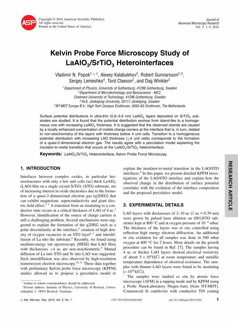
In order to prove the applicability of KPFM to planarstudies of LAO/STO interfaces, a surface of 4 uc thicklayer was lithographically masked and 3× 3 m squareswere irradiated by 250 eV Ar+ ions. After that the pho-toresist mask was removed. AFM and KPFM images ofone of these squares are presented in Figure 1. The AFMimage shows a smooth LAO surface with terraces origi-nating from atomic steps of the slightly miscut STO sur-face. The KPFM image does not reproduce topography, butrather demonstrates a clear difference in surface potentialbetween the unirradiated and irradiated areas. The unirra-diated area has much lower potential. It can be interpretedas a lower charge density due to suppressed dipole for-mation caused by the presence of the conductive interfacewhich electrically shields the LAO layer from the STO.On the other hand, the LAO layer inside the irradiated areais amorphized and the conductive interface is destroyed(the squares become insulating). The numerous structuraldefects (especially vacancies) give rise to charge carri-ers favouring a dipole formation under the bias appliedbetween tip and surface. This explains much higher valuesof the surface potential inside the irradiated squares.
(a)
(b)
Fig. 1. (a) AFM and (b) KPFM images of LAO/STO sample with 4 ucthick LAO layer. The LAO layer is radiation-damaged and conductivity ofthe interface is destroyed inside the centrally positioned square. The smallbumps at the square perimeter in (a) correspond to residual photoresist.
2 J. Adv. Microsc. Res. 5, 1–5, 2010
RESEARCH
ARTIC
LE
Popok et al. Kelvin Probe Force Microscopy Study of LaAlO3/SrTiO3 Heterointerfaces
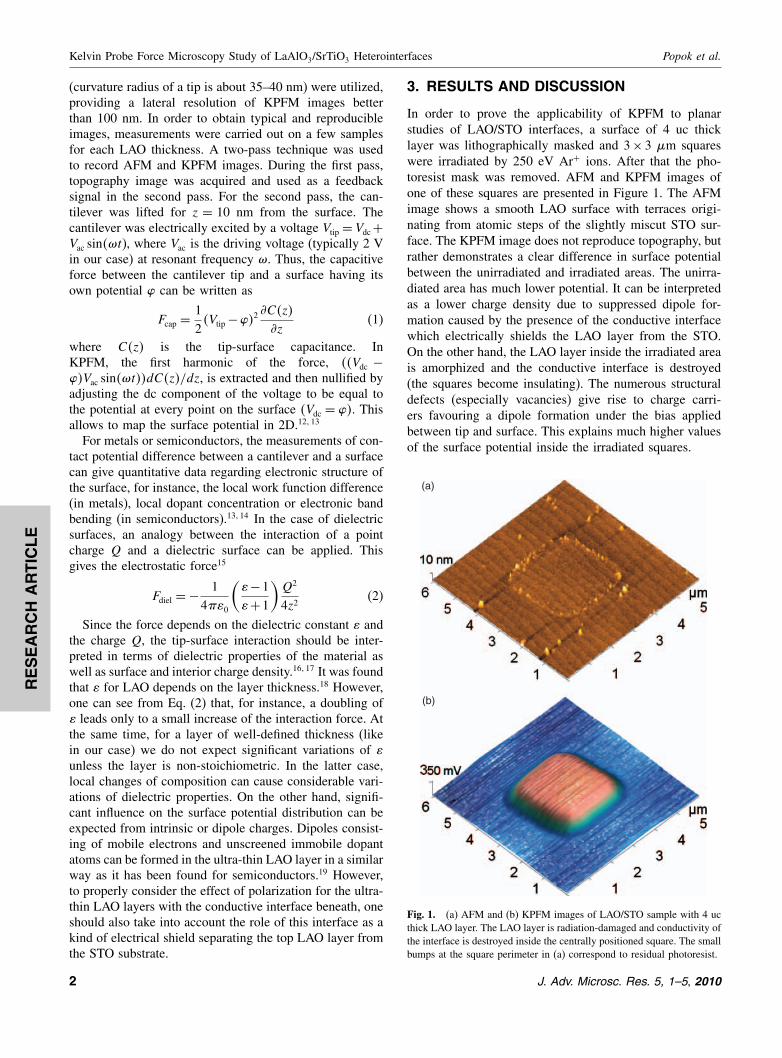
Now we switch to the as-grown and annealed samples(i.e., without radiation damage). Typical surface potentialimage from bare STO substrate is presented in Figure 2(a).The scale on the right-hand side shows the relative varia-tion of the potential with respect to a mean value. The STOsubstrate demonstrates rather homogeneous distribution ofthe surface potential that indicates absence of significantvariations of the dielectric properties and surface charges.The image in Figure 2(b) corresponds to 2 uc thick LAOlayer deposited on the STO. This image is a typical one,i.e., similar surface potential distributions were observedon other samples with 2 uc thick LAO layer. Moreover,samples with 3 uc thick layer demonstrate same type ofthe island-like potential images and therefore not shown.Pronounced island-like structure presented in Figure 2(b)is rather different from that found for bare STO. This typeof island-like structure is observed in considerable numberof scans over the same area, thus, eliminating possible con-tribution of surface contaminants. The surface potential of4 uc thick layer changes back to an almost homogeneous
(a) (b)
(c) (d)
Fig. 2. KPFM images of (a) bare STO substrate and LAO/STO samples with (b) 2, (c) 4 and (d) 6 uc thick LAO layer.
(or slightly mosaic-like) distribution, see Figure 2(c). Fur-ther increase of thickness up to 6 uc leads to a homoge-neous potential distribution (Fig. 2(d)), very similar to thatobserved on bare STO.The island-like type of surface potential distribution
found for 2 and 3 uc thick layers can be related to theformation of areas rich in mobile charge carriers at theLAO/STO interface, thus affecting local polarization ofthe ultra-thin LAO layers. Formation of these areas maybe caused by a local change of composition. This is sup-ported by MEIS results indicating non-stoichiometry inthin (≤3 uc) LAO layers.9 In particular, deficiency of Lawas found in the layers and La diffusion into STO wassuggested. Substitution of Sr by La is one possible sourcefor increased concentration of charge carriers at the inter-face. We do not also exclude that charge carriers originatefrom oxygen-vacancies in the STO.6�7 It should be empha-sised that the areas with increased concentration of mobilecharge carries in 2 and 3 uc thick films do not provide acontinuous (or quasi-continuous) conductive path.
J. Adv. Microsc. Res. 5, 1–5, 2010 3
RESEARCH
ARTIC
LE
Kelvin Probe Force Microscopy Study of LaAlO3/SrTiO3 Heterointerfaces Popok et al.
The change from island-like to almost homogeneouspotential distribution with increase of the layer thick-ness from 3 to 4 uc can be interpreted in terms of achange of surface composition towards a stoichiometricone, which is observed using MEIS.9 The stoichiometryexcludes considerable local variations of composition andconsequently dielectric properties at surface thus elimi-nating inhomogeneity in the surface potential distribution.One should also consider the formation of a conductiveinterface between two dielectrics which acts as an elec-trical shield separating the LAO layer from the STO sub-strate. This prevents possible local contributions of chargesfrom the STO substrate on the potential measured at theLAO surface. Thus, the samples with 4 uc thick layer rep-resent a boundary case of insulator-to-metal transition inconductance. This transition is evidenced by KPFM as achange of the surface potential distribution from island-like towards a homogeneous one. The potential distributionbecomes even more homogeneous for the samples with
(a)
(b)
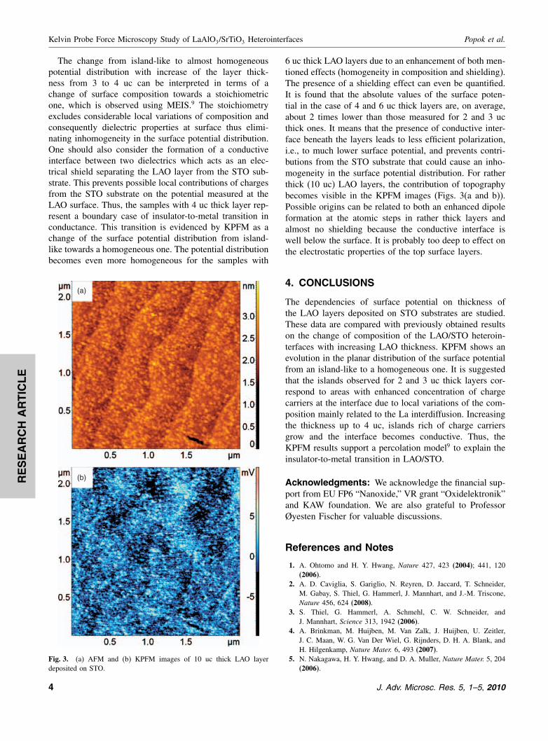
Fig. 3. (a) AFM and (b) KPFM images of 10 uc thick LAO layerdeposited on STO.
6 uc thick LAO layers due to an enhancement of both men-tioned effects (homogeneity in composition and shielding).The presence of a shielding effect can even be quantified.It is found that the absolute values of the surface poten-tial in the case of 4 and 6 uc thick layers are, on average,about 2 times lower than those measured for 2 and 3 ucthick ones. It means that the presence of conductive inter-face beneath the layers leads to less efficient polarization,i.e., to much lower surface potential, and prevents contri-butions from the STO substrate that could cause an inho-mogeneity in the surface potential distribution. For ratherthick (10 uc) LAO layers, the contribution of topographybecomes visible in the KPFM images (Figs. 3(a and b)).Possible origins can be related to both an enhanced dipoleformation at the atomic steps in rather thick layers andalmost no shielding because the conductive interface iswell below the surface. It is probably too deep to effect onthe electrostatic properties of the top surface layers.
4. CONCLUSIONS
The dependencies of surface potential on thickness ofthe LAO layers deposited on STO substrates are studied.These data are compared with previously obtained resultson the change of composition of the LAO/STO heteroin-terfaces with increasing LAO thickness. KPFM shows anevolution in the planar distribution of the surface potentialfrom an island-like to a homogeneous one. It is suggestedthat the islands observed for 2 and 3 uc thick layers cor-respond to areas with enhanced concentration of chargecarriers at the interface due to local variations of the com-position mainly related to the La interdiffusion. Increasingthe thickness up to 4 uc, islands rich of charge carriersgrow and the interface becomes conductive. Thus, theKPFM results support a percolation model9 to explain theinsulator-to-metal transition in LAO/STO.
Acknowledgments: We acknowledge the financial sup-port from EU FP6 “Nanoxide,” VR grant “Oxidelektronik”and KAW foundation. We are also grateful to ProfessorØyesten Fischer for valuable discussions.
References and Notes
1. A. Ohtomo and H. Y. Hwang, Nature 427, 423 (2004); 441, 120(2006).
2. A. D. Caviglia, S. Gariglio, N. Reyren, D. Jaccard, T. Schneider,M. Gabay, S. Thiel, G. Hammerl, J. Mannhart, and J.-M. Triscone,Nature 456, 624 (2008).
3. S. Thiel, G. Hammerl, A. Schmehl, C. W. Schneider, andJ. Mannhart, Science 313, 1942 (2006).
4. A. Brinkman, M. Huijben, M. Van Zalk, J. Huijben, U. Zeitler,J. C. Maan, W. G. Van Der Wiel, G. Rijnders, D. H. A. Blank, andH. Hilgenkamp, Nature Mater. 6, 493 (2007).
5. N. Nakagawa, H. Y. Hwang, and D. A. Muller, Nature Mater. 5, 204(2006).
4 J. Adv. Microsc. Res. 5, 1–5, 2010

RESEARCH
ARTIC
LE
Popok et al. Kelvin Probe Force Microscopy Study of LaAlO3/SrTiO3 Heterointerfaces
6. W. Siemons G. Koster, H. Yamamoto, W. A. Harrison, G. Lukovsky,T. H. Geballe, D. H. A. Blank, and M. R. Beasley, Phys. Rev. Lett.98, 196802 (2007).
7. A. Kalabukhov, R. Gunnarsson, J. Börjesson, E. Olsson, T. Claeson,and D. Winkler, Phys. Rev. B 75, 121404(R) (2007).
8. P. R. Willmott, S. A. Pauli, R. Herger, C. M. Schleputz, D. Kumah,C. Cionca, and Y. Yacoby, Phys. Rev. Lett. 99, 155502 (2007).
9. A. Kalabukhov, Yu. A. Boikov, I. T. Serenkov, V. I. Sakharov,V. N. Popok, R. Gunnarsson, J. Börjesson, N. Ljustina, E. Olsson,D. Winkler, and T. Claeson, Phys. Rev. Lett. 103, 146101 (2009).
10. C. L. Jia, S. B. Mi, M. Faley, U. Poppe, J. Schubert, and K. Urban,Phys. Rev. B 79, 081405(R) (2009).
11. J. Börjesson, PhD Thesis, Chalmers University of Technology,Gothenburg (2009).
12. M. Nonnenmacher, M. O’Boyle, and H. K. Wickramasinghe, Appl.Phys. Lett. 58, 2921 (1991).
13. Y. Rosenwaks, R. Shikler, Th. Glatzel, and S. Sadewasser, Phys.Rev. B 70, 085320 (2004).
14. H. Huang, H. Wang, J. Zhang, and D. Yan, Appl. Phys. A 95, 125(2009).
15. J. D. Jackson, Classical Electrodynamics, Wiley, New York(1998).
16. S. Kalinin and D. A. Bonnell, Phys. Rev. B 62, 10419 (2000).17. Y. Shen, D. M. Barnett, and P. M. Pinsky, Rev. Sci. Instrum.
79, 023711 (2008).18. L. Yan, Semicond. Sci. Technol. 19, 935 (2004).19. C. Baumgart, M. Helm, and H. Schmidt, Phys. Rev. B 80, 085305
(2009).
Received: 24 March 2010. Accepted: 26 April 2010.
J. Adv. Microsc. Res. 5, 1–5, 2010 5