keynote paper statistical timing analysis: from basic...
TRANSCRIPT

IEEE TRANSACTIONS ON COMPUTER-AIDED DESIGN OF INTEGRATED CIRCUITS AND SYSTEMS, VOL. 27, NO. 4, APRIL 2008 589
Keynote PaperStatistical Timing Analysis: From Basic
Principles to State of the ArtDavid Blaauw, Senior Member, IEEE, Kaviraj Chopra, Student Member, IEEE,
Ashish Srivastava, and Lou Scheffer, Senior Member, IEEE
Abstract—Static-timing analysis (STA) has been one of the mostpervasive and successful analysis engines in the design of digitalcircuits for the last 20 years. However, in recent years, the in-creased loss of predictability in semiconductor devices has raisedconcern over the ability of STA to effectively model statisticalvariations. This has resulted in extensive research in the so-calledstatistical STA (SSTA), which marks a significant departure fromthe traditional STA framework. In this paper, we review the recentdevelopments in SSTA. We first discuss its underlying modelsand assumptions, then survey the major approaches, and close bydiscussing its remaining key challenges.
Index Terms—Algorithm, circuit, performance, process varia-tions, timing analysis.
I. INTRODUCTION
S INCE the early 1990s, static-timing analysis (STA) hasbeen a widely adopted tool for all facets of very-large-
scale-integration chip design. STA is not only the universaltiming sign-off tool but also lies at the heart of numeroustiming optimization tools. The main advantage of STA overvector-based timing simulation is that it does not rely on inputvectors, which can be difficult to construct and can easilymiss an obscure performance-limiting path in the circuit. Thewidespread use of STA can be attributed to several factors:1) The basic STA algorithm is linear in runtime with circuit size,allowing analysis of designs in excess of 10 million instances;1
2) the basic STA analysis is conservative in the sense that itwill overestimate the delay of long paths in the circuit andunderestimate the delay of short paths in the circuit. This makesthe analysis “safe,” guaranteeing that the design will functionat least as fast as predicted and will not suffer from hold-timeviolations; 3) the STA algorithms have become fairly mature,addressing critical timing issues such as interconnect analysis,
Manuscript received September 13, 2006; revised February 12, 2007. Thispaper was recommended by Associate Editor S. Vrudhula.
D. Blaauw and K. Chopra are with the University of Michigan, Ann Arbor,MI 48109 USA.
A. Srivastava is with the Magma Design Automation, Austin, TX78759 USA.
L. Scheffer is with the Cadence Design System, San Jose, CA 95134 USA.Digital Object Identifier 10.1109/TCAD.2007.907047
1As discussed in Section III, the propagation of arrival times throughthe combinational portion of a circuit using the critical-path-method (CPM)algorithm has a runtime that is linear with circuit size. However, industrial STAtools often include methods for common-path removal in the clocking networkand for false-path elimination. These methods have a higher runtime complexitythan the simple CPM algorithm.
accurate delay modeling, false or multicycle paths, etc; and4) delay characterization for cell libraries is clearly defined,forms an effective interface between the foundry and the designteam, and is readily available.
Traditional STA tools are deterministic and compute thecircuit delay for a specific process condition. Hence, all pa-rameters that impact the delay of a circuit, such as devicegate length and oxide thickness, as well as operating voltageand temperature, are assumed to be fixed and are uniformlyapplied to all the devices in the design. In this paper, we referto traditional deterministic STA as DSTA. In DSTA, processvariation is modeled by running the analysis multiple times,each at a different process condition. For each process conditiona so-called corner file is created that specifies the delay ofthe gates at that process condition. By analyzing a sufficientnumber of process conditions the delay of the circuit underprocess variation can be bounded.
The fundamental weakness of DSTA is that while globalshifts in the process (referred to as die-to-die variations) canbe approximated by creating multiple corner files, there is nostatistically rigorous method for modeling variations acrossa die (referred to as within-die variations).2 However, withprocess scaling progressing well into the nanometer regime,process variations have become significantly more pronouncedand within-die variations have become a non-negligible com-ponent of the total variation. We will show later in this paperthat the inability of DSTA to model within-die variation canresult in either an over- or underestimate of the circuit delay,depending on the circuit topology. Hence, DSTA’s desirableproperty of being conservative may no longer hold for certaincircuit topologies while, at the same time, DSTA may be overlypessimistic for other circuit topologies. The accuracy of DSTAin advanced processes is therefore a serious concern.
In addition to the growing importance of within-die processvariations, the total number of process parameters that exhibitsignificant variation has also increased [1]. Hence, even the
2While the deterministic model of gate delay as used in DSTA excludesa statistical treatment of across-die variation, industry tools have over timedeveloped a number of methods to approximate the impact of such variations.A common method is to use a predetermined delay scaling factor for all circuitelements (delay is increased for long-path analysis and is decreased for short-path analysis). However, if the scaling factor is set to the worst-case within-dievariation, the analysis becomes exceedingly pessimistic. On the other hand,lesser values cannot be proved to be conservative, negating one of the majoradvantages of DSTA.
0278-0070/$25.00 © 2008 IEEE
Authorized licensed use limited to: IEEE Xplore. Downloaded on November 14, 2008 at 14:26 from IEEE Xplore. Restrictions apply.

590 IEEE TRANSACTIONS ON COMPUTER-AIDED DESIGN OF INTEGRATED CIRCUITS AND SYSTEMS, VOL. 27, NO. 4, APRIL 2008
modeling of only die-to-die variations in DSTA now requiresan untenable number of corner files. For instance, in addition todevice parameters, interconnect parameters must be considered,and which combination of interconnect and device parametersresults in the worst-case (or best-case) delay often depends onthe circuit structure. In an attempt to capture the worst-case die-to-die variation for all cases, the number of corner files used inindustry has risen sharply. It is now common to use more thana dozen corner files [2], whereas the number can even exceed100, thereby increasing the effective runtime of DSTA by oneorder of magnitude or more.
The need for an effective modeling of process variationsin timing analysis has led to extensive research in statisticalSTA. Some of the initial research works date back to the veryintroduction of timing analysis in the 1960s [3] as well as theearly 1990s [4], [5]. However, the vast majority of researchworks on SSTA date from the last five years, with well overa hundred papers published in this research field since 2001.In this paper, we give a brief review of the different issues andapproaches to SSTA. In Section II, we examine the differentsources of uncertainty and their impact on circuit performance.In Section III, we present the formulation of the SSTA problemand discuss its key challenges and approaches. In Section IV,we discuss the so-called “block-based” approaches in moredetail and present their strengths and weaknesses. Section Vdiscusses the remaining key issues that must be addressed tobring SSTA to a level of maturity that approaches that of theDSTA today. We conclude this review paper in Section VI.
II. SOURCES OF TIMING VARIATION
In this section, we discuss the key sources of variation intiming prediction, that make timing analysis a challenging taskfor nanoscale digital circuits. We first discuss different types ofuncertainties that arise as a design moves from specification toimplementation and final operation in the field. We then focuson process variations in more detail and discuss the distinctionbetween die-to-die and within-die variations and the source ofso-called spatial correlations. Finally, we discuss the impact ofdifferent types of process variations on the timing of a circuit.
A. Process, Environmental, and Model Uncertainties
The uncertainty in the timing estimate of a design can beclassified into three main categories:
1) modeling and analysis errors—inaccuracy in device mod-els, in extraction and reduction of interconnect parasitics,and in timing-analysis algorithms;
2) manufacturing variations—uncertainty in the parametersof fabricated devices and interconnects from die to dieand within a particular die;
3) operating context variations—uncertainty in the operat-ing environment of a particular device during its lifetime,such as temperature, supply voltage, mode of operation,and lifetime wear-out.
To illustrate each of these uncertainties, consider the stagesof design, from initial specification to final operation, as shownin Fig. 1. The design process starts with a broad specification
Fig. 1. Steps of the design process and their resulting timing uncertainties.
of the design and then goes through several implementationsteps, such as logic synthesis, buffer insertion, and place androute. At each step, timing analysis is used to guide the designprocess. However, timing analysis is subject to a host of inac-curacies, such as undetected false paths, cell-delay error, errorin interconnect parasitics, SPICE models, etc. These modelingand analysis errors result in a deviation between the expectedperformance of the design and its actual performance charac-teristics. For instance, the STA tool might utilize a conservativedelay-noise algorithm resulting in certain paths operating fasterthan expected.
In the next stage, the design is fabricated and each individualdie incurs additional manufacturing-related variations due toequipment imprecisions and process limitations. Finally, a man-ufactured die is used in an application such as a cell phone ora laptop. Each particular die then sees different environmentalconditions, depending on its usage and location. Since environ-mental factors such as temperature, supply voltage, and workload affect the performance of a die, they give rise to the thirdclass of uncertainty. To achieve the required timing specifica-tion for all used die throughout their entire lifetime, the designermust consider all three sources of uncertainty. However, a keydifference between the three classes of uncertainty is that eachhas a sample space that lies along a different dimension. Hence,each class of uncertainty calls for a different analysis approach.
First, we recall that the sample space of an experiment ora random trial is the set of all possible outcomes. The timinguncertainty caused by modeling and analysis errors has as itssample space the set of design implementations resulting frommultiple design attempts. Each design attempt results in animplementation which triggers particular inaccuracies in themodels and tools, resulting in a timing distribution across thissample space. However, a design is typically implemented onlyonce and there needs to be a high level of confidence that theconstraints will be met in the first attempt. Hence, the designeris interested in the worst-case timing across this sample space.Thus, margins are typically added to the models to createsufficient confidence that they are conservative and will resultin a successful implementation. Although a statistical analysisof model and analysis uncertainty is uncommon, it could aidin a more accurate computation of the delay with a specifiedconfidence level.
In the case of process variations, the sample space is theset of manufactured die. In this case, a small portion ofthe sample space is allowed to fail the timing requirements
Authorized licensed use limited to: IEEE Xplore. Downloaded on November 14, 2008 at 14:26 from IEEE Xplore. Restrictions apply.

BLAAUW et al.: STATISTICAL TIMING ANALYSIS: FROM BASIC PRINCIPLES TO STATE OF THE ART 591
since those die can be discarded after manufacturing. Thisconsiderably relaxes the timing constraints on the design andallows designers to significantly improve other performancemetrics, such as power dissipation. In microprocessor design, itis common to perform so-called binning where die are targetedto different applications based on their performance level. Thislessens the requirement that all or a very high percentage of thesample space meets the fastest timing constraint. Instead, eachperformance level in the sample space represents a differentprofit margin, and the total profit must be maximized.
The sample space of environmental uncertainty is across theoperational life of a part and includes variations in temperature,modes of operation, executed instructions, supply voltage, life-time wear-out, etc. Similar to model and analysis uncertainty,the chip is expected to function properly throughout its oper-ational lifetime in all specified operating environments. Evenif a design fails only under a highly unusual environmentalcondition, the percentage of parts that will fail at some pointduring their operational life can still be very high. Therefore,a pessimistic analysis is required to ensure a high confidenceof correct operation throughout the entire lifetime of the part.Naturally, this approach results in a design that operates fasterthan necessary for much of its operational life, leading to aloss in efficiency. For instance, when a part is operating at atypical ambient temperature the device sizing or supply voltagecould be relaxed, reducing power consumption. One approachto address this inefficiency is to use runtime adaptivity of thedesign [6], [7].
Since each of the three discussed variabilities representsorthogonal sample spaces, it is difficult to perform a com-bined analysis in a meaningful manner. Environmental uncer-tainty and uncertainty due to modeling and analysis errors aretypically modeled using worst-case margins, whereas uncer-tainty in process is generally treated statistically. Hence, mostSSTA research works, as well as this paper, focus only onmodeling process variations. However, the accuracy gained bymoving from DSTA to SSTA methods must be considered inlight of the errors that continue to exist due to the other sourcesof timing error, such as analysis and modeling error, uncertaintyin operating conditions, and lifetime wear-out phenomena. Wediscuss in the next section the sources of process variation inmore detail.
B. Sources of Process Variation
1) Physical Parameters, Electrical Parameters, and DelayVariation: The semiconductor manufacturing process has be-come more complex, at the same time process control preci-sion is struggling to maintain relative accuracy with continuedprocess scaling. As a result, a number of steps throughoutthe manufacturing process are prone to fluctuations. Theseinclude effects due to chemical mechanical polishing (CMP),which is used to planarize insulating oxides and metal lines,optical proximity effects, which are a consequence of patterningfeatures smaller than the wavelength of light [8]–[10], and lensimperfections in the optical system. These, as well as othernumerous effects, cause variation of device and interconnectphysical parameters such as gate length (or critical dimension—
Fig. 2. Physical parameter variations resulting in electrical parameter varia-tions, which, in turn, result in circuit-delay variations.
CD), gate-oxide thickness, channel doping concentration, in-terconnect thickness and height, etc., as shown in Fig. 2.Among these, CD variation and channel doping fluctuationshave typically been considered as dominant factors. However,many SSTA methods model a much wider range of physicalparameters. Variations in these physical parameters, in turn,result in variations in electrical device characteristics, suchas the threshold voltage, the drive strength of transistors, andthe resistance and capacitance of interconnects. Finally, thevariations in electrical characteristics of circuit componentsresult in delay variations of the circuit.
It is important to note that more than one electrical parametermay have a dependence on a particular physical parameter. Forexample, both resistance and capacitance of an interconnect areaffected by variation in wire width. An increase in interconnectwidth reduces the separation between wires, resulting in anincreased coupling capacitance while decreasing the resistanceof the wire. Similarly, perturbations in the gate-oxide thicknessinfluence the drive current, the threshold voltage, and the gatecapacitance of the transistors. Dependence of two or moreelectrical parameters on a common physical parameter givesrise to correlation of these electrical parameters and ignoringthis correlation can result in inaccurate results. For instance,if we ignore the negative correlation between capacitance andresistance, there is a nonzero probability that both resistanceand capacitance are at their worst-case values. However, thisis physically impossible and leads to unrealistic RC delayestimates. In [11], the authors present a method to determine theprocess-parameter values that result in a more realistic worst-case delay estimate.
Along similar lines, a particular equipment variation canimpact multiple physical-parameter values, resulting in a corre-lation of the physical parameters themselves. For instance, con-sider the physical-parameter variations due to lens aberration. Ifmultiple masks are illuminated with the same lens, the variationof all metal layers and even polysilicon will be correlated.3 InSection IV, we will discuss methods for modeling correlatedparameters using a smaller number of independent parameters,such as principal component analysis.
It would be ideal to model each process step in the manu-facturing process to determine the variations and correlationsin the physical parameters. However, such an analysis is com-plex and impractical due to the number of equipment-relatedparameters in each fabrication step and the total number ofsteps. Hence, most SSTA approaches have taken the physical
3Multiple scanners may be used to manufacture a particular part. This canreduce the discussed correlation here but may not eliminate it.
Authorized licensed use limited to: IEEE Xplore. Downloaded on November 14, 2008 at 14:26 from IEEE Xplore. Restrictions apply.

592 IEEE TRANSACTIONS ON COMPUTER-AIDED DESIGN OF INTEGRATED CIRCUITS AND SYSTEMS, VOL. 27, NO. 4, APRIL 2008
Fig. 3. Taxonomy of process variations.
parameters themselves (such as CD, doping concentration, andoxide thickness) to be the basic random variables (RVs). Thesevariables are either assumed to be independent or to have well-understood correlations.2) Classification of Physical-Parameter Variation:
Physical-parameter variations can be classified based onwhether they are deterministic or statistical and based on thespatial scale over which they operate, as shown in Fig. 3.
1) Systematic variations are components of physical-parameter variation that follow a well-understood be-havior and can be predicted upfront by analyzing thedesigned layout. Systematic variations arise in large partfrom optimal proximity effects, CMP, and its associatedmetal fill. These layout-dependent variations can be mod-eled premanufacturing by performing a detailed analysisof the layout. Therefore, the impact of such variationscan be accounted for using deterministic analysis at laterstages of the design process [12], [13] and particularlyat timing sign-off. However, since we do not have layoutinformation early in the design process, it is common totreat these variations statistically. In addition, the modelsrequired for analysis of these systematic variations areoften not available to a designer, which makes it advanta-geous to treat them statistically, particularly when it is un-likely that all effects will assume their worst-case values.
2) Nonsystematic or random variations represent the trulyuncertain component of physical-parameter variations.They result from processes that are orthogonal to thedesign implementation. For these parameters, only thestatistical characteristics are known at design time, andhence, they must be modeled using RVs throughout thedesign process. Line-edge roughness (LER) and random-dopant fluctuations (RDF) are examples of nonsystematicrandom sources of variation.
It is common that earlier in the design flow, both systematicand nonsystematic variations are modeled statistically. As wemove through the design process and more detailed informa-tion is obtained, the systematic components can be modeleddeterministically, if sufficient analysis capabilities are in place,thereby reducing the overall variability of the design.3) Spatial Reach of Variations: Nonsystematic variations
can be further analyzed by observing that different sources of
variations act on different spatial scales. Some parameters shiftwhen the equipment is loaded with a new wafer or betweenprocessing one lot of wafers to the next—this can be due tosmall unavoidable changes in the alignment of the wafers in theequipment, changes in the calibration of the equipment betweenwafer lot processing, etc. On the other hand, some shift can oc-cur between the exposure of different reticles on a wafer, result-ing in reticle-to-reticle variations. A reticle is the area of a waferthat is simultaneously exposed to the mask pattern by a scanner.The reticle is approximately 20 mm × 30 mm and will typicallycontain multiple copies of the same chip layout or multipledifferent chip layouts. At each exposure, the scanner is alignedto the previously completed process steps, giving rise to avariation in the physical parameters from one reticle to the next.Finally, some shift can occur during the reticle exposure itself.For instance, a shift in a parameter, such as laser intensity, mayoccur while a particular reticle is scanned leading to within-reticle variations. Another example is non-uniform etch con-centration across the reticle, leading to the variation in the CD.
These different spatial scales of variation give rise to aclassification of nonsystematic variations into two categories.
1) Die-to-die variations (also referred to as global or interdievariations) affect all the devices on the same die in thesame way. For instance, they cause the CD of all deviceson the same chip to be larger or smaller than nominal. Wecan see that die-to-die variations are the result of shiftsin the process that occur from lot to lot, wafer to wafer,reticle to reticle, and across a reticle if the reticle containsmore than one copy of a chip layout.
2) Within-die variations (also referred to as local or intradievariations) affect each device on the same die differently.In other words, some devices on a die have a smaller CD,whereas other devices on the same die have a larger CDthan nominal. Within-die variations are only caused byacross-reticle variations within the confines of a singlechip layout.
Finally, within-die variations can be categorized intospatially correlated and independent variations as discussed asfollows.
1) Spatially correlated variations. Many of the underlyingprocesses that give rise to within-die variation changegradually from one location to the next. Hence, theseprocesses tend to affect closely spaced devices in a similarmanner, making them more likely to have similar charac-teristics than those placed far apart. The component ofvariation that exhibits such spatial dependence is knownas spatially correlated variation. We discuss the modelingof spatial correlated device parameters in more detail inSection IV-B1.
2) Independent variations. The residual variability of a de-vice that is statistically independent from all other devicesand does not exhibit spatially dependent correlations isreferred to as independent variation.4 These variations in-clude effects such as RDF and LER. It has been observed
4In the SSTA literature, this independent component of nonsystematicprocess variation is often referred to as the random component. However, thisis an unfortunate misnomer since all nonsystematic variations are random.
Authorized licensed use limited to: IEEE Xplore. Downloaded on November 14, 2008 at 14:26 from IEEE Xplore. Restrictions apply.

BLAAUW et al.: STATISTICAL TIMING ANALYSIS: FROM BASIC PRINCIPLES TO STATE OF THE ART 593
that with continued process scaling, the contribution ofindependent within-die variation is increasing. Modelssuch as those of Pelgrom et al. [14], which express theamount of independent variation as a function of nominaldevice parameters, are gaining increased importance.
C. Impact of Correlation on Circuit Delay
As discussed in the previous section, nonsystematic processvariations must be modeled using RVs. Furthermore, the RVsassociated with different gates in a design will be partially cor-related due to the joint contributions from die-to-die, spatiallycorrelated, and independent process-variation components. Aswe shall discuss in Section IV, this partial correlation createssignificant difficulties for SSTA. The analysis can be substan-tially simplified if the RVs are assumed to be either fullycorrelated with a correlation coefficient of 1 or are assumedcompletely independent. If the RVs are assumed to be fullycorrelated, the variation has the same characteristics as die-to-die variation, and DSTA can be used to bound the circuitdelay using a set of corner files. On the other hand, whilethe assumption of independence requires a statistical-analysisapproach it significantly simplifies the required operations.
In this section, we investigate the error that is introduced inthe timing analysis of a combinational-circuit block under ei-ther the fully correlated or independent assumption. This is use-ful since traditional DSTA approaches have often made the fullycorrelated assumption, whereas early SSTA work has madean independence assumption. We will show that, dependingon the circuit topology, either assumption can yield conserv-ative or optimistic timing estimates. In the succeeding discus-sion, we first consider the simple case of a single path and thentreat the maximum delay of multiple paths. Finally, we notesome of the complexities involved when clocking is considered.1) Delay of a Single Path: If the gate delays along a path are
independent, then they tend to average out in the overall pathdelay. For example, let a path have n gates connected in serieswith each gate having an independent normal-delay distributionP1, P2, . . . , Pn with the same mean µ and standard deviation σ.The σ/µ ratio of the path delay relative to that of the gate delayis given by (
σ
µ
)path
=1√n
(σ
µ
)gate
. (1)
However, if the gate-delay distributions Pi are correlated witha correlation coefficient ρ, the σ/µ ratio for the path delaybecomes (
σ
µ
)path
=
√1 + ρ(n − 1)
n
(σ
µ
)gate
. (2)
In both cases, the standard deviation of the path delay in-creases with the number of gates in the path. However, the ratioσ/µ scales as 1/
√(n) with the assumption of independence,
whereas it remains constant under the fully correlated assump-tion (ρ = 1). Hence, an assumption that the partially correlatedRVs along a path are fully correlated will overestimate thespread of path delay. The delay specified at a confidence
Fig. 4. Maximum of two normal-delay distributions with identical mean andvariance having different correlations.
Fig. 5. Mean and variance of the maximum of two identical normal RVs as afunction of correlation coefficients.
point greater than 50%5 will be overestimated, resulting in apessimistic analysis. On the other hand, assuming all variationsto be independent along a path results in an optimistic estimateof delay (at yield points greater than 50%).2) Maximum of Multiple Paths: The delay of a
combinational-circuit block is obtained by taking the maximumof the delays of all the paths in the circuit. This maximum againdepends on the correlation of the gate delays. To illustratethis, we consider a circuit consisting of two paths, each withnormal distributed delays with a mean of 750 ps and a standarddeviation of 100 ps. If we assume that all of the gate delays inthe circuit are fully correlated with ρ = 1, the two path delayswill also be perfectly correlated. On the other hand, if the gatedelays are assumed to be independent, the two path delays willbe independent. Fig. 4 shows the probability distribution of themaximum of the two path delays assuming perfect correlation(ρ = 1), partial correlation (ρ = 0.5), and independent pathdelays (ρ = 0). It can be seen that the probability distributionfor the independent case always gives a higher delay than thatin the two positively correlated cases. Hence, the independenceassumption will overestimate delay and vice versa. Thisconcept is mathematically known as Slepian’s inequality.Intuitively, when the two path delays are independent, thenumber of cases in the sample space, where at least one of thetwo delays is toward the high end of the distribution, is muchgreater compared to the correlated case.
Fig. 5 shows the mean and variance of the maximum of thetwo path delays as a function of their correlation coefficient.The mean of the maximum delay decreases with increased
5For long-path delay analysis, delay is typically computed at confidencepoints greater than 50%, whereas, for short-path delay analysis, the confidencepoint is typically placed < 50%. In both cases, overestimation of ρ results in apessimistic analysis.
Authorized licensed use limited to: IEEE Xplore. Downloaded on November 14, 2008 at 14:26 from IEEE Xplore. Restrictions apply.

594 IEEE TRANSACTIONS ON COMPUTER-AIDED DESIGN OF INTEGRATED CIRCUITS AND SYSTEMS, VOL. 27, NO. 4, APRIL 2008
correlation, whereas the standard deviation increases. There-fore, the independence assumption will underestimate the delayspread. Note also that the maximum of the two identical normalpath-delay distributions does not result in a normal distributionexcept under the fully correlated assumption. We will discussthis effect in more detail in Section III.
Given a combinational-circuit block, the overall circuitdelay maybe either over- or underestimated by both the fullycorrelated and independence assumptions. The fully correlatedassumption will overestimate the delay of individual paths,whereas it will underestimate the maximum of those pathdelays. Hence, the final outcome depends on the topology of thecircuit. If the logic depth of the circuit is large while, at the sametime, only a few paths are critical, the overestimation along thecritical paths will dominate, resulting in a pessimistic analysisresult. On the other hand, for circuits with shallow logic depthand highly balanced paths, the underestimation occurring in themaximum computation will dominate, and the analysis will beoptimistic under the fully correlated assumption. The inverse istrue for the independence assumption.
Finally, when considering sequential circuits, the delay vari-ation in the buffered clock tree must be considered. In general,the fully correlated assumption will underestimate the variationin the arrival times at the leaf nodes of the clock tree, whichwill tend to overestimate circuit performance. However, wemust also consider the correlation between the delays in thecombinational logic and the clock tree, in which case theanalysis becomes more complex.
III. PROBLEM FORMULATION AND BASIC
SOLUTION APPROACHES
A. Problem Formulation
The traditional DSTA procedure abstracts a timing graphfrom a combinational circuit. The nodes of the timing graphrepresent primary inputs/outputs of the circuit and gate in-put/output pins. Its edges represent the timing elements of thecircuit, namely, the gate input-pin–output-pin delay and wiredelay from a driver to a receiver, as shown in Fig. 6. The weighton these edges represents the delay of the corresponding timingelement. For a combinational circuit, it is convenient to connectall primary inputs to a virtual source node with virtual edgeshaving weight equal to the input arrival times. Similarly, all theprimary outputs are connected to a virtual sink node throughvirtual edges with weights representing the required arrivaltimes. The resulting timing graph, therefore, has a single sourceand sink node.
A similar timing graph can be constructed for sequentialcircuits. Fig. 7 shows the additional timing elements pertainingto a clock network (i.e., the launch and capture paths of theclock tree) and the sequential elements. In the correspond-ing timing graph, the virtual source node corresponds to theinput driver of the on-chip clock network. The clock-driverdelays and interconnect delays on the launch path, the clock-to-q delay, and the setup times of the sequential elements are againmodeled using weights on their corresponding graph edges.Similarly, the virtual sink node also corresponds to the clockinput driver, and the capture path is represented with nodes and
Fig. 6. Example circuit in (a) and its timing graph in (b).
edges in the timing graph. In this case, however, the weightsof edges corresponding to the capture path are assigned withnegative delay values as opposed to the positive values forthe launch path. Apart from this distinction, the timing graphsfor flip-flop-based sequential circuits are a direct extension ofthose for the combinational circuits and can be analyzed withthe same timing algorithms. However, significant complicationsarise when transparent latches are used in place of flip-flops orwhen the launch and capture paths of the clock tree share thesame drivers, as is common.
As discussed in Section II, device parameters such as gatelength, doping concentration, and metal thickness must betreated as RVs due to process variation. The delay of each edge,being a function of these parameters, also becomes an RV. Thisallows us to extend the concept of the traditional timing graphto a statistical timing graph defined as follows.Definition: A timing graph G = {N,E, ns, nf} is a directed
graph having exactly one source node ns and one sink nodenf , where N is a set of nodes, and E is a set of edges. Theweight associated with an edge corresponds to either the gatedelay or the interconnect delay. The timing graph is said to be astatistical timing graph if ith edge weight di is an RV.
The arrival time at the source node of the timing graphtypically has a deterministic zero value. This reflects the factthat in combinational timing graphs, clock-tree skew is notrepresented, whereas in sequential circuits, the source node ispulled back to a common point on the launching and capturingclock paths.6 In traditional DSTA, the most basic goal of theanalysis is to find the maximum delay between the source nodeand the sink node of a timing graph, which is the delay ofthe longest path in the circuit. When modeling process-induceddelay variations, the sample space is the set of all manufactureddies. In this case, the device parameters will have differentvalues across this sample space, hence the critical path and itsdelay will change from one die to the next. Therefore, the delay
6Note that a deterministic value at the source node of a sequential timinggraph does not account for jitter from the Phase Locked Loop (PLL) or othersources.
Authorized licensed use limited to: IEEE Xplore. Downloaded on November 14, 2008 at 14:26 from IEEE Xplore. Restrictions apply.

BLAAUW et al.: STATISTICAL TIMING ANALYSIS: FROM BASIC PRINCIPLES TO STATE OF THE ART 595
Fig. 7. Timing elements of a sequential circuit path (a) and its timing graph (b).
Fig. 8. PDF and CDF.
of the circuit is also an RV, and the first task of SSTA isto compute the characteristics of this RV. This is performedby computing its probability-distribution function (PDF) orcumulative-distribution function (CDF) (see Fig. 8). Alterna-tively, only specific statistical characteristics of the distribution,such as its mean and standard deviation, can be computed.Note that the CDF and the PDF can be derived from oneanother through differentiation and integration. Given the CDFof circuit delay of a design and the required performanceconstraint the anticipated yield can be determined from theCDF. Conversely, given the CDF of the circuit delay and therequired yield, the maximum frequency at which the set ofyielding chips can be operated at can be found.Definition: Let a path pi be a set of ordered edges from the
source node to the sink node in G, and let Di be the path-lengthdistribution of pi, computed as the sum of the weights d forall edges k on the path. Finding the distribution of Dmax =maximum(D1, . . . , Di, . . . , Dnpaths) among all paths (indexedfrom 1 to n paths) in the graph G is referred to as the SSTAproblem of a circuit.
Similar to traditional DSTA, we can formulate the SSTAproblem as that of finding the latest arrival-time distributionat the sink node in the timing graph [15], [16]. The latestarrival-time distribution at the sink node can be found bypropagating the arrival time from the source node through thetiming edges while computing the latest arrival-time at every
node in topological order. Subsequently, the latest arrival-timedistribution at the sink node is the circuit-delay distribution. Itis worth noting that the basic DSTA algorithm is based on theproject-planning technique known as the CPM and involves asimple topological traversal [17]. Likewise, the basic SSTA for-mulation for circuit designs was first motivated from the projectevaluation and review technique (PERT) literature [3], [18].However, in contrast to DSTA, PERT was shown to be anN-P complete problem [19].
In addition to the problem of finding the delay of the circuit,which we have posed as the basic SSTA problem, it is alsokey to improve this delay when the timing requirements arenot met. Hence, DSTA methods typically report the slack ateach node in the circuit, in addition to the circuit delay andcritical paths. The slack of a node is the difference between thelatest time a signal can arrive at that node, such that the timingconstraints of the circuit are satisfied (referred to as the requiredtime), and the actual latest arrival time of the signal at that node[20]. Similar to the circuit delay, the slack of a node is an RVin the SSTA formulation. Due to space limitation, we will notdiscuss efficient methods for slack computation in this paper butrefer to the pertinent literature in Section V. We also will notdiscuss latch-based sequential timing analysis, which involvesmultiple-phase clocks, cycle stealing, clock-schedule verifica-tion, etc. Methods for statistical sequential timing analysis us-ing latches and clock-skew analysis can be found in [21]–[25].
B. Challenges in SSTA
The statistical formulation of timing analysis introduces sev-eral new modeling and algorithmic issues that make SSTA acomplex and enduring research topic [26]. In this section, weintroduce some of these issues, as well as the relevant SSTAterminology.1) Topological Correlation: Paths that start with one or
more common edges after which the paths separate and join
Authorized licensed use limited to: IEEE Xplore. Downloaded on November 14, 2008 at 14:26 from IEEE Xplore. Restrictions apply.

596 IEEE TRANSACTIONS ON COMPUTER-AIDED DESIGN OF INTEGRATED CIRCUITS AND SYSTEMS, VOL. 27, NO. 4, APRIL 2008
again at a later node are called reconvergent paths and the nodeat which these paths reconverge is called the reconvergent node.For instance, in Fig. 6, the two paths P1 and P2 share thesame first edge (corresponding to gate g1) and reconverge atthe output of gate g0 (node r). In such case, the input arrivaltimes at the reconvergent node become dependent on each otherbecause of the shared edge delay. This dependence leads toso-called topological correlation between the arrival times andcomplicates the maximum operation at the reconvergent node.To perform accurate analysis, the SSTA algorithm must captureand propagate this correlation so that it is correctly accountedfor during the computation of the maximum function.2) Spatial Correlation: As discussed in Section II-B,
within-die variation of the physical device parameters oftenexhibits spatial correlation, giving rise to correlation betweenthe gate delays. Hence, if the gates that comprise two paths havespatially correlated device parameters they will have correlatedpath delays. In this way, correlation can be introduced betweenpaths that do not share any common timing edges. For instance,in Fig. 6, the paths P1 and P3 do not share any common delayedges, but if gates g1 and g2 are within close proximity on thedie, their spatially correlated delays can give rise to correlationbetween the two path delays. Hence, spatial correlation of thearrival times must be captured and propagated during SSTA sothat it is correctly accounted for during the maximum operation.Spatial correlation also impacts the sum operation. For exam-ple, if in Fig. 6, gates g1 and g3 have spatially correlated delaysthen the arrival time at node p will be correlated with the delayof gate g3.
While topological correlation only affects the maximumoperation, spatial correlation affects both the sum operationand the maximum operation. This raises two fundamentalchallenges for SSTA: 1) how to model gate delays and arrivaltimes such that the spatial correlation of the underlying deviceparameters can be expressed; and 2) given a model of the spatialcorrelation, how to propagate and preserve the correlationinformation while performing the sum and maximum opera-tions in SSTA. A common approach to this problem has beento represent delay in terms of the device-parameter-space basis,which is common to all gate delays. This approach is discussedin more detail in Section IV.3) Nonnormal Process Parameters and Nonlinear Delay
Models: Normal or Gaussian distributions are found to be themost commonly observed distributions for RVs, and a numberof elegant analytical results exist for them in the statisticsliterature. Hence, most of the initial work in SSTA assumednormal distributions for physical device parameters, electricaldevice parameters, gate delays, and arrival times. However,some physical device parameters may have significantly non-normal distributions. In this section, we discuss the source andimpact of such nonnormal distributions.
An example of a nonnormal device parameter is CD (orgate length) due to the variation in depth of focus (DOF).As a result of equipment limitations and nonplanarity of thedie, the focus point of the exposed image on the die exhibitssome amount of variation. This impacts the development ofthe photoresist layer and consequently impacts the CD of thedevice. However, both large and small values of the DOF result
Fig. 9. Nonnormal CD distribution due to nonlinear dependence of CDon DOF.
in an underdevelopment of the photoresist and the dependenceof CD on the DOF is nonlinear. Even if the variation ofDOF is normal, the CD variation will decidedly be nonnormal.As shown in Fig. 9, the PDF of CD is clearly (negatively)skewed and nonnormal.7
Even if the physical device parameters are indeed normallydistributed (e.g., doping concentration has a normal distribu-tion), the dependence of the electrical device parameters andgate delay on these physical parameters may not be linear,giving rise to nonnormal gate delays. Initial work in modelingspatial correlations [27]–[29] used a first-order delay modelwhich assumed a linear dependence of the gate delay on phys-ical device parameters. If the variations are small, this linearapproximation is justified, as the error introduced by ignoringhigher order terms is negligible. However, with reduction ofgeometries, process variation is becoming more pronounced,and the linear approximation may not be accurate for someparameters.
Nonnormal delay and arrival-time distributions introducesignificant challenges for efficient SSTA. While this is a rela-tively new area of research, several researchers have proposedapproaches to address this issue [30]–[35]. Finally, it should benoted that apart from the difficulty of modeling the nonnormal-ity of an individual RV, the dependence between two nonnormalRVs is no longer expressed by a simple correlation factor. Thisfurther complicates the correct treatment of topological andspatial correlations.4) Skewness Due to Maximum Operation: Even if gate de-
lays are assumed to be normal, SSTA has to cope with the
7A probability distribution is said to have negative skewness if it has a longtail in the negative direction of the RV, such as the CD distribution shown inFig. 9. Conversely, a positive skewness indicates a long tail in the positivedirection.
Authorized licensed use limited to: IEEE Xplore. Downloaded on November 14, 2008 at 14:26 from IEEE Xplore. Restrictions apply.

BLAAUW et al.: STATISTICAL TIMING ANALYSIS: FROM BASIC PRINCIPLES TO STATE OF THE ART 597
fact that the maximum operation is an inherently nonlinearfunction. The maximum of two normal arrival times will resultin a nonnormal arrival time that is typically positively skewed.8
In addition, the nonnormal arrival-time distribution produced atone node is the input to the maximum computation at down-stream nodes. Hence, a maximum operation that can operate onnonnormal arrival times is required.
Most of the existing approaches ignore the skewness intro-duced by the maximum operation and approximate the arrivaltimes with normal distributions. The error of this normal ap-proximation is larger if the input arrival times have similarmeans and dissimilar variances [36]. In other words, the erroris most pronounced when two converging paths have nomi-nally balanced path delays, but one path has a tighter delaydistribution than the other. This can occur in a circuit whentwo paths with equal nominal delay have a different number ofgates or when the correlation among their gates differs. Anotherexample is when one path is dominated by interconnect delaywhile the other is dominated by gate delay.
An example of such two delay distributions is shown inFig. 10(a). Intuitively, we can see that RV B will dominate themaximum delay for values greater than its mean since B hassignificantly higher probabilities in this range. For delay valuesbelow the mean, RV A will dominate. Since A and B havedifferent variance, skew is introduced in their maximum. Fortwo input distributions that have identical means and variances,the resulting maximum exhibits smaller skewness [Fig. 10(b)].Finally, Fig. 10(c) shows that if the means of the input dis-tributions are significantly different, the resulting maximum isentirely dominated by one distribution, and skew is negligible.
The aforementioned issues address four basic challengesin SSTA, which have received significant attention in the lit-erature. However, many other critical challenges to the de-velopment of a mature SSTA tool remain. For instance, theavailability of statistical data remains difficult. This, and otherchallenges in SSTA, will be discussed in Section V.
C. SSTA Solution Approaches
We now give a brief overview of the principle approachesto SSTA, moving from traditional methods to more recentapproaches.1) Numerical-Integration Method: The simplest SSTA ap-
proach follows directly from the problem definition givenin Section III-A. A numerical integration over the process-parameter space is performed to compute the yield of thecircuit for a particular delay. Typically, the delay of a set ofcritical paths is expressed as a linear function of the physicaldevice parameters and a feasible region in this parameter spaceis defined by the desired circuit delay. This region is thennumerically integrated, exploring all possible permutations ofphysical device-parameter values that lie in the feasible region.Efficient numerical-integration methods were proposed in [37].The advantage of this method is that it is completely general and
8It is possible to obtain much more complex distributions, such as bimodaldistributions, even when the input parameters remain normal. While suchoccurrence is rare, they introduce significant modeling difficulties.
Fig. 10. Skewness due to nonlinear maximum operation for different inputdistributions.
process variation with any type of distribution and correlationcan be modeled. However, it can be quite expensive in runtime,in particular for balanced circuits with a large number ofcritical paths.2) Monte Carlo Methods: The second general approach per-
forms a statistical sampling of the sample space using MonteCarlo simulation, based on the Metropolis sampling algorithm[38]. Instead of explicitly enumerating the entire sample space,the key idea is to identify the regions of significant probabilityand to sufficiently sample these regions. Using the PDF of thephysical device parameters, a number of samples are drawn. Foreach sample, the circuit delay is computed using the traditionalDSTA methods. Thereafter, by evaluating a fraction of samplesthat meet the timing constraint, an estimate of timing yieldis found. If a sufficient number of samples are drawn, theestimation error is small. By sweeping the timing constraintand finding the yield for each value, the entire circuit-delaydistribution can be found.
As with numerical integration, the Monte Carlo approachhas the advantage of being completely general. Furthermore,it is based on existing mature DSTA methods and performs sig-nificantly faster than the numerical integration-based methods.However, since DSTA is in the inner loop of the Monte Carlo
Authorized licensed use limited to: IEEE Xplore. Downloaded on November 14, 2008 at 14:26 from IEEE Xplore. Restrictions apply.

598 IEEE TRANSACTIONS ON COMPUTER-AIDED DESIGN OF INTEGRATED CIRCUITS AND SYSTEMS, VOL. 27, NO. 4, APRIL 2008
simulation, the runtime can still be significant, particularlyif a fully featured industrial DSTA tool is used. Using theMonte Carlo simulation, it is also difficult to perform incre-mental analysis after a designer makes a small change to thecircuit. It has been shown that the performance of MonteCarlo techniques can be improved using methods such asimportance sampling [2], [39]–[41]. However, more research isrequired to examine if fast sampling techniques can be effectivefor SSTA.3) Probabilistic Analysis Methods: Both previous ap-
proaches are based on sample-space enumeration. In contrast,probabilistic methods explicitly model gate delay and arrivaltimes with RVs. These methods typically propagate arrivaltimes through the timing graph by performing statistical sumand maximum operations.9 They can be classified into twobroad classes: 1) path-based approaches; and 2) block-basedapproaches. The key difference between the two approaches iswhere in the algorithm the maximum function is invoked.
Path-based approaches: In path-based SSTA algorithms,a set of paths, which is likely to become critical, is identi-fied, and a statistical analysis is performed over these pathsto approximate the circuit-delay distribution. First, the delaydistribution of each path is found by summing the delay of allits edges. Assuming normal gate delays, the path-delay distri-bution is normal and can be analytically computed [42]–[44].The overall circuit-delay distribution is then found by perform-ing a statistical maximum operation over all the path delays(discussed in more detail in Section IV).
The basic advantage of this approach is that the analysis isclearly split into two parts—the computation of path delaysfollowed by the statistical maximum operation over these pathdelays. Hence, much of the initial research in SSTA wasfocused on path-based approaches [5], [42], [43], [45]–[48].Clearly, the difficulty with the approach is how to rigorouslyfind a subset of candidate paths such that no path that hassignificant probability of being critical in the parameter space isexcluded. In addition, for balanced circuits, the number of pathsthat must be considered can be very high. Therefore, most of thelater research has focused on the block-based approaches.
One of the methods that fall in the path-based categoryapproximates the statistical delay of a circuit early in the designprocess when the exact gate-level implementation is not yetknown [49], [50]. In this work, the circuit is modeled usinga set of generic paths whose specifications are provided bythe designer. The method also determines the settings of thetransistor-level electrical parameters that give a specific yieldgoal. These settings can then be used in a traditional deter-ministic timing verification flow. The usefulness of applyingSSTA methods early in the design process, when exact gate-level implementations are not yet available, depends on the rel-ative magnitude of the delay uncertainty introduced by processvariations versus the uncertainty due to the undetermined circuitimplementation.
9The minimum operation is also needed for the computation of the shortestpath, clock skew, and slack computations. However, it can be derived from themaximum operation.
Block-based approaches: The block-based methods fol-low the DSTA algorithm more closely and traverse the circuitgraph in a topological manner. The arrival time at each node iscomputed using two basic operations: 1) For all fan-in edgesof a particular node, the edge delay is added to the arrival-timeat the source node of the edge using the sum operation; and2) given these resulting arrival times, the final arrival time atthe node is computed using the maximum operation. Hence, theblock-based SSTA methods propagate exactly two arrival times(a rise and a fall arrival time) at each circuit node, resulting ina runtime that is linear with circuit size. The computation ofthe sum function is typically not difficult; however, finding thestatistical maximum of two correlated arrival times is not trivial.
Due to its runtime advantage, many current research andcommercial efforts have taken the block-based approach. Fur-thermore, unlike other approaches, the block-based approachlends itself to incremental analysis which is advantageousfor diagnostic/optimization applications. In block-based SSTAmethods, the result of the maximum operation performed at onenode is the input to the maximum operation which is performedat downstream nodes. It is therefore essential that the sumand maximum operations preserve the correlation informationof the arrival times so that this information is available atlater operations. Furthermore, the skewness introduced by themaximum operation must be considered.
IV. BLOCK-BASED SSTA
In this section we discuss block-based SSTA methods inmore detail. The different methods are presented in order ofincreasing complexity. We start with simpler early methodsthat were based on a normal independent approximation ofthe arrival times. We then discuss methods that model topo-logical correlation due to reconvergence of arrival times. Thisis followed by a number of methods that account for spatialwithin-die variations. Finally, we briefly survey more recentlyproposed nonlinear and nonnormal block-based methods.
A. Distribution Propagation Approaches (Gate-Delay Space)
Initial efforts in block-based SSTA approaches focused ondirectly representing gate delays with RVs characterized bytheir distribution or statistical characteristics. The commontechnique employed by all these approaches is to explicitlypropagate the arrival-time distributions through the timinggraph. This is achieved by employing a statistical sum operatorto compute the sum of the timing arc delay and the source-nodearrival-time distribution. In the case of multifan-in nodes, astatistical maximum operator is also applied to the arrival timescorresponding to different fan-in edges of a node.
A basic block-based SSTA algorithm based on a PERT-liketraversal was first given in [3]. Later, Berkelaar [51] presenteda linear-runtime algorithm for propagating mean and varianceof timing variables. In this approach, both gate delays and latestarrival-time distributions are assumed to be independent normalRVs. Based on these simplifying assumptions, the sum andmaximum of arrival-time RVs are computed using analyticalresults for the normal RVs.
Authorized licensed use limited to: IEEE Xplore. Downloaded on November 14, 2008 at 14:26 from IEEE Xplore. Restrictions apply.

BLAAUW et al.: STATISTICAL TIMING ANALYSIS: FROM BASIC PRINCIPLES TO STATE OF THE ART 599
Fig. 11. Shift with scaling and grouping techniques to perform convolution ofinput and gate-delay PDFs to compute the output-delay PDF.
In [52], the authors extend this analytical approach to han-dle topological correlation due to reconvergent paths, andcorrelation between edge delays that correspond to the samegate, at the cost of increased complexity. The approach uses thestatistical sum operation to reduce series edges in the timinggraph to a single edge. At each step of the reduction, thecorrelation of the reduced edge with the edges with whichit has nonzero correlation is recomputed. A similar reductionprocedure is then performed for parallel edges using the statis-tical maximum operation under the normal assumption usingthe analytical results given in [36]. This maximum operationis explained in more detail in the following section. The pro-posed approach limits the number of edges whose correlationinformation is stored in the memory by identifying those nodeswhose correlation information is no longer required. This ap-proach was extended in [53] and [54] by assigning a level toeach node in the directed acyclic graph (DAG) using a depth-first search. The level is used to identify the nodes whosecorrelation information can be discarded at each stage of thearrival-time propagation.
In [55]–[57], the authors propose an alternative discreterepresentation for relaxing the normal-distribution assumption.The gate delays are now modeled as discrete delay distribu-tions that are generated by sampling a continuous distribution.Note that the discrete PDFs are renormalized after sampling toensure that the sum of the probabilities for the discrete eventsis equal to one.
The approach then utilizes discrete sum and maximum oper-ations for arrival-time propagation. In the case of a degenerateor deterministic input-delay distribution, the sum operation issimple, and the output-delay PDF is obtained by simply shiftingthe gate-delay distribution by the input delay. However, inthe case where the input-delay PDF is nondegenerate, a setof shifted output-delay distributions is generated, as shown inFig. 11. Each of these shifted PDFs corresponds to a discreteevent from the input-delay PDF. This set of shifted PDFs isthen combined using Bayes’ theorem—the shifted PDFs arefirst scaled, where the scaling factor is the probability of theassociated discrete input event. The scaled events are thengrouped by summing the probability at each of the discretetime points. The actual probability of an event can be obtainedby dividing the total value for each discrete point of the PDFby the sum of the numbers corresponding to all the events in
each discrete PDF. The overall computation can be succinctlyexpressed as
fs(t) =∞∑
i=−∞fx(i)fy(i − t) = fx(t) � fy(t) (3)
where s = x + y, and implies that the PDF of the sum of twoRVs can be expressed as a convolution of their PDFs.
The statistical maximum is computed using the relation
fz(t) = Fx(t) fx(t) + Fy(t)fy(t) (4)
where z = maximum(x, y), f and F represent the PDF andCDF of the RV, respectively, and x and y are assumed to beindependent. The previous equation expresses mathematicallythat the probability that the maximum of two discrete RVshas a value t0 is equal to the probability that one of the RVshas a value equal to t0 and the other has a value less than orequal to t0.
For handling topological correlation due to reconvergentpaths, a partitioning-based approach is used to decompose thecircuit into the so-called supergates. Each supergate is a subcir-cuit with a single fan-out and one or more inputs, all of whichare statistically independent. The discrete events at the inputs ofthe supergates are propagated separately, and the resulting dis-tributions are finally combined at the output of the supergate us-ing Bayes’ theorem. The process of separately propagating eachof the discrete events of the PDFs is referred to as enumeration.Special care has to be taken in the case where a multifan-outnode lies in the fan-out cone of another multifan-out node. Un-fortunately, the runtime complexity of this algorithm dependson the circuit structure and is exponential in the worst case.
The authors in [15], [58], and [59] extend the work onhandling topological correlation while using the same dis-crete framework for representing PDFs. The authors presentan approach to determine the minimum set of nodes, whichneeds to be enumerated to handle reconvergence exactly. Asexpected, the worst-case computational complexity of enumer-ation remains exponential. Nevertheless, the authors show theuseful property that ignoring topological correlation results ina distribution that is a stochastic upper bound on the exactdistribution of the circuit delay. A stochastic upper bound of adelay distribution with CDF P (t) is a distribution whose CDFQ(t) has a value which is always smaller than or equal to P (t)for all values of t, as shown in Fig. 12. Such an upper boundresults in a pessimistic estimate of the timing yield of the circuitat a given performance target.
Based on this result, the authors developed a linear-runtimemethod for computing both lower and upper bounds on theexact delay distribution of the circuit. These bounds are thenused to obtain an estimate of the circuit delay at a desiredconfidence point, as well as the accuracy of the bounds. In thecase when the bounds are not sufficiently close to each other,a heuristic method is used to iteratively improve the boundsusing selective enumeration of a subset of the nodes. Theresults presented in [15] showed that performing enumerationat a small set of carefully selected nodes leads to a significantimprovement in the quality of the bounds. This is due to the
Authorized licensed use limited to: IEEE Xplore. Downloaded on November 14, 2008 at 14:26 from IEEE Xplore. Restrictions apply.

600 IEEE TRANSACTIONS ON COMPUTER-AIDED DESIGN OF INTEGRATED CIRCUITS AND SYSTEMS, VOL. 27, NO. 4, APRIL 2008
Fig. 12. Upper bound of a delay CDF provides a conservative estimate ofcircuit delay for a given timing yield.
fact that correlation between two arrival times only impacts themaximum computation if the two arrival times have comparablemeans. Hence, the correlation between two arrival times thatare substantially shifted can be ignored without incurring sig-nificant error.
In a related work [60], a Bayesian-network-based approachfor representing the statistical timing graph is presented forhanding topological correlations. The Bayesian-network for-mulation prescribes an efficient method to factorize the jointdistribution over the entire timing graph into an optimal setof factors. Although the worst-case runtime complexity ofsuch an approach remains exponential, the complexity growsexponentially with the size of the largest clique in the circuit,which, in practice, is found to grow much more slowly than thecircuit size.
In [61], the authors modeled arrival times as CDFs and delaysas PDFs. Using a piecewise linear model for CDFs and PDFs,they present a computationally simple expression for perform-ing the sum and maximum operations. Furthermore, they alsopresented a method for handling reconvergent fan-outs usinga dependence list associated with every arrival time, whichare propagated through the circuit and pruned for increasedefficiency. Using error budgeting, an approach to optimize theruntime of this method was presented in [62]. A method togenerate device-level discrete delay distributions from the un-derlying process-parameter distribution was presented in [63].
B. Dependence Propagation Approaches (Parameter Space)
In the previous section, we discussed techniques that con-sider topological correlations. The next crucial step in thedevelopment of block-based SSTA was to account for spatialcorrelation of the underlying physical device parameters. Thebasic difference between the two cases is that the correlationamong arrival times now originates from the correlation of thedevice parameters. In addition, an arrival time at the input of agate can be correlated with the delay of the gate itself, impact-ing the sum operation in addition to the maximum operation.
In the distribution propagation approaches, the gate delaysare the basic RVs in the formulation. However, to model thecorrelation in the physical device parameters, it is necessary tomodel these device parameters themselves as the basic RVs.The delay of the gates is therefore expressed as a function(linear or nonlinear) of the physical or electrical device param-
Fig. 13. Principal components of two positively correlated RVs.
eters. It is this functional form that expresses the dependenceof the gate delays on the device parameters, which is propa-gated through the circuit. This concept of representing delaydependences with a parametric delay model was first introducedin [64]. To enable such techniques, it is necessary to developa model of the spatial correlation of the device parameters.Therefore, we first discuss some of the models for expressingthe correlation of device parameters and then show how thesecan be used to compute the final circuit delay.1) Correlation Models: To exactly model spatial correlation
between the physical parameters of two devices, a separate RVis required for each device. However, the correlation betweentwo devices is generally a slow monotonically decreasing func-tion of their separation, decaying over distances of hundreds ofmicrometers. Therefore, simplified correlation structures usinga grid model [29] or quadtree model [28] have been proposed.These models allow the correlation among gates of the die to beexpressed using a smaller set of RVs.
In a grid model, the overall die area is divided using a squaregrid. It is assumed that the grid size is chosen such that all gateswithin a single square on the grid can be assumed to have per-fectly correlated spatial variations. Let us now consider the RVsrequired to model variations in a given process parameter. Eachsquare in the grid corresponds to an RV of a device parameter,which has correlations to all other RVs corresponding to theother squares. To simplify the correlation structure of the RVs,this set of correlated RVs is mapped to another set of mutuallyindependent RVs with zero mean and unit variance using theprincipal components of the original set of correlated RVs.The original RVs are then expressed as a linear combinationof the principal components. These principal components canbe obtained by performing an eigenvalue decomposition of thecorrelation matrix, as explained in more detail in [65].
Intuitively, this is shown in Fig. 13 where the distribution oftwo correlated jointly normal RVs A and B is shown. In thescatter plot, the x-axis is the value of A, whereas the y-axisis the value of B. If A and B were independent, the scatterplot would form a perfect circle or a horizontal or vertical oval.The diagonal distribution shown indicates positive correlationbetween A and B since large values of A tend to correspondto large values of B. The principal-component-analysis (PCA)method expresses A and B using two new RVs C and D, usingthe rotated axes r and s. RVs A and B can be expressed usinga linear combination of C and D. Furthermore, the rotation ofr and s ensures that C and D are independent.
It is important to note that constructing the correlation matrixdirectly from a distance-based correlation function may result
Authorized licensed use limited to: IEEE Xplore. Downloaded on November 14, 2008 at 14:26 from IEEE Xplore. Restrictions apply.

BLAAUW et al.: STATISTICAL TIMING ANALYSIS: FROM BASIC PRINCIPLES TO STATE OF THE ART 601
Fig. 14. Modeling spatial correlation using quadtree partitioning. Thenumbering of regions in different levels is shown in the figure. A region(i, j) intersects the regions (i + 1, 4j − 3)−(i + 1, 4j).
in a nonpositive-definite matrix. Furthermore, the correlationmatrix must be positive definite and that this condition may beviolated if the matrix is constructed from an arbitrary distance-based function or from measured data (especially if noisy).Hence, some techniques, such as replacing all negative eigen-values by zero, may need to be used. This problem has beeninvestigated in [66]–[71].
The quadtree model proposed in [28] and [43] also parti-tions the overall die area into a number of regions. However,instead of using PCA to express the correlated componentsof variations, it uses an additive approach to consider thespatial dependence of process parameters. This is achieved byrecursively dividing the area of the die into four equal parts,which is known as quadtree partitioning. As the regions of thedie are recursively divided into parts, the number of parts ateach level increases by a factor of four, as shown in Fig. 14.Each partition, at all levels of the quadtree, is assigned with anindependent RV. The spatially correlated variation associatedwith a gate is then defined to be the sum of the RV associatedwith the lowest level partition that contains the gate and theRVs at each of the higher partitioning levels that intersectsthe position of the gate. The correlation among gates arisesfrom the sharing of some of the RVs at higher levels of thequadtree. The number of shared RVs depends on the distancebetween the two gates. Moreover, a larger fraction of thevariance can be allocated at higher levels of the quadtree if theparameter is known to be more strongly correlated over largedistances. In [72], a method for determining the values of theRVs associated with each partition is presented.
An alternative grid-based model was proposed in [33] whereonly four RVs are used to model the correlation structure. Thefour RVs are assumed to be associated with the four corners ofa die, and the RVs associated with the gates inside the designare represented as a weighted sum of these four RVs, where theweighting coefficients are functions of the distance between theposition of a gate and each of the four corners of the die.
In [73], the authors use the Karhunen–Loeve expansion(KLE) to express the distance-based correlation function interms of a set of RVs and an orthonormal set of deterministic
functions related to the position of a gate on the die. This allowsthe correlation to be expressed as a continuous function ofthe location of a gate. In addition, the authors show that KLEprovides much greater accuracy as compared to PCA of a gridmodel [29], or equivalently, it provides similar accuracy with areduction in the number of RVs.2) Propagation of Delay Dependence on Parameter Varia-
tions: All the described correlation models share the commoncharacteristic that the set of correlated device parameters isrepresented by a (typically linear) function of independent RVs.In block-based SSTA, this representation of the correlation isthen carried over to the delay and signal arrival times, whichare represented in a so-called canonical form. In this section,we will assume that the canonical form is a linear function ofnormal RVs, which allows us to express the canonical form as
da = µa +n∑i
aizi + an+1R (5)
where µa is the mean delay, zi represents the n independentRVs used to express the spatially correlated device-parametervariations, R represents the residual independent variation, andcoefficients a′
is represent the sensitivity of delay to each of theRVs. The crucial step is to express the results of both the sumand maximum operations in canonical form. This allows theexpression of the arrival time to be maintained in canonicalform during propagation through the timing graph. This in turnenables the use of a single sum and maximum operation at alllocations in the timing graph.
The first operation requires the computation of the sum C oftwo delay distributions A and B, C = A + B, where A, B, andC are expressed in canonical form. Due to the nature of the sumoperation, C can be easily expressed in canonical form, and itscoefficients can be computed as
µc = µa + µb (6)
ci = ai + bi ∀i : 1 ≤ i ≤ n (7)
cn+1 =√
a2n+1 + b2
n+1. (8)
Note that since the last term represents independent varia-tions, it is not correlated with the canonical expressions for Aand B. The overall contribution of these independent variationsto C is therefore obtained by computing the root sum square ofthe individual independent contributions.
The second operation requires the computation of C =maximum(A, B). Since the maximum is a nonlinear function,the maximum of two canonical forms cannot be expressedexactly in canonical form. Hence, the authors in [27] and [29]propose the following algorithm for computing a statisticalapproximation Capprox of the maximum of two arrival timesA and B.
1) Compute variances and covariance of A and B
σ2a =
n+1∑i=1
a2i , σ2
b =n+1∑i=1
b2i , r =
n∑i=1
aibi. (9)
Authorized licensed use limited to: IEEE Xplore. Downloaded on November 14, 2008 at 14:26 from IEEE Xplore. Restrictions apply.
602 IEEE TRANSACTIONS ON COMPUTER-AIDED DESIGN OF INTEGRATED CIRCUITS AND SYSTEMS, VOL. 27, NO. 4, APRIL 2008
2) Compute tightness probability TA = P (A > B) (theprobability that arrival time A is larger than B) as pre-sented in [36]
TA = Φ(
µa − µb
θ
)(10)
where
Φ(x) =
x∫−∞
φ(x)dx (11)
φ(x) =1√2π
e−x2
2 (12)
θ =√
σ2A + σ2
B − 2r. (13)
3) Compute mean and variance of C = maximum(A,B)using the results from Clark’s work [36]
µc =µaTA + µb(1 − TA) + θφ
(µa − µb
θ
)(14)
σ2c =
(µa + σ2
a
)TA +
(µb + σ2
b
)(1 − TA)
+ (µa + µb)θφ(
µa − µb
θ
)− µ2
c . (15)
4) Compute sensitivity coefficient ci of Capprox using thetightness probability
ci = aiTA + bi(1 − TA) ∀i : 1 ≤ i ≤ n. (16)
5) Compute sensitivity coefficient cn+1 of canonical formCapprox to make the variance of Capprox equal to the vari-ance of C = maximum(A,B). It was shown in [74] thata valid cn+1 always exists as the residue (σ2
c −∑n
i c2i ) is
always greater than or equal to zero.
The approach effectively computes the first two moments ofC in aforementioned steps 1)–3) and then approximates themaximum using a canonical form in steps 4)–5). The coeffi-cients associated with z′is are obtained by computing the sum ofthe two canonical models weighted by their respective tightnessprobabilities, whereas the coefficient of the independent term isdetermined to match the variance of Capprox and C. In addition,this approximation was shown to match the correlation of C andthe z′is [29].
In [28], the authors propose a similar canonical form. How-ever, the independent component of variation is propagated as adiscretized delay distribution. The assumption of normal RVs inthe canonical form is relaxed, whereas the PDF of the indepen-dent variables is assumed to be bounded. The sum operation isperformed as mentioned previously. However, the independentterm of the sum is obtained by numerically convolving thetwo independent distributions. The maximum of two PDFs is
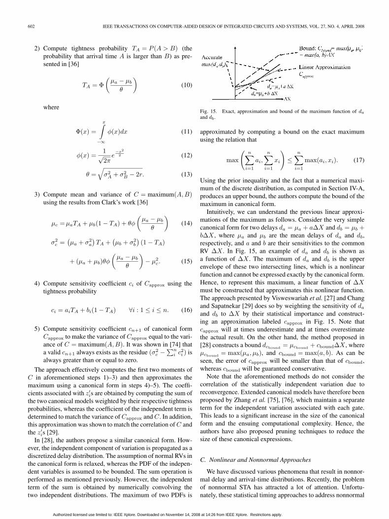
Fig. 15. Exact, approximation and bound of the maximum function of da
and db.
approximated by computing a bound on the exact maximumusing the relation that
max
(n∑
i=1
ai,
n∑i=1
xi
)≤
n∑i=1
max(ai, xi). (17)
Using the prior inequality and the fact that a numerical maxi-mum of the discrete distribution, as computed in Section IV-A,produces an upper bound, the authors compute the bound of themaximum in canonical form.
Intuitively, we can understand the previous linear approxi-mations of the maximum as follows. Consider the very simplecanonical form for two delays da = µa + a∆X and db = µb +b∆X , where µa and µb are the mean delays of da and db,respectively, and a and b are their sensitivities to the commonRV ∆X . In Fig. 15, an example of da and db is shown asa function of ∆X . The maximum of da and db is the upperenvelope of these two intersecting lines, which is a nonlinearfunction and cannot be expressed exactly by the canonical form.Hence, to represent this maximum, a linear function of ∆Xmust be constructed that approximates this nonlinear function.The approach presented by Visweswariah et al. [27] and Changand Sapatnekar [29] does so by weighting the sensitivity of da
and db to ∆X by their statistical importance and construct-ing an approximation labeled capprox in Fig. 15. Note thatcapprox will at times underestimate and at times overestimatethe actual result. On the other hand, the method proposed in[28] constructs a bound dcbound = µcbound + cbound∆X , whereµcbound = max(µa, µb), and cbound = max(a, b). As can beseen, the error of capprox will be smaller than that of cbound,whereas cbound will be guaranteed conservative.
Note that the aforementioned methods do not consider thecorrelation of the statistically independent variation due toreconvergence. Extended canonical models have therefore beenproposed by Zhang et al. [75], [76], which maintain a separateterm for the independent variation associated with each gate.This leads to a significant increase in the size of the canonicalform and the ensuing computational complexity. Hence, theauthors have also proposed pruning techniques to reduce thesize of these canonical expressions.
C. Nonlinear and Nonnormal Approaches
We have discussed various phenomena that result in nonnor-mal delay and arrival-time distributions. Recently, the problemof nonnormal STA has attracted a lot of attention. Unfortu-nately, these statistical timing approaches to address nonnormal
Authorized licensed use limited to: IEEE Xplore. Downloaded on November 14, 2008 at 14:26 from IEEE Xplore. Restrictions apply.

BLAAUW et al.: STATISTICAL TIMING ANALYSIS: FROM BASIC PRINCIPLES TO STATE OF THE ART 603
physical device-parameter distributions or nonlinear delay de-pendences incur significant computational overheads.
In [31], [32], and [77], the authors extend the linear canon-ical delay model to include quadratic dependences on deviceparameters. Following a PCA analysis of the set of correlateddevice parameters, the canonical form can be expressed as
da = µa +n∑i
aizi +n∑
i=1
n∑j=1
bijzizj + an+1R. (18)
To enable arrival-time computations using such a quadraticdelay model, we need to define the sum and maximum oper-ations using quadratic canonical expressions. The sum of twoexpressions in quadratic form can be readily seen to result ina quadratic canonical form. In [31], the authors use momentmatching to calculate the maximum, again expressed in thequadratic canonical form, where the moments are calculatedusing numerical integration. The same problem is handled usinga conditional linear maximum operation in [32]. The condi-tional maximum operation implies that the maximum operationis carried out only under the condition that the resulting dis-tribution has a small skew. An estimate of the skewness of themaximum is obtained by assuming the two input distributionsto be normal RVs with the same mean, variance, and correlation(as the original RVs) and then using Clark’s expression [36] toestimate the skew of the maximum. If the skewness is above thethreshold, the maximum is postponed, and both distributionsare propagated through the circuit as a set. If the skewness isbelow a threshold, the maximum is computed at that node. Tolimit the number of distributions being propagated through eachnode of the DAG, two distributions are immediately replaced bytheir maximum as soon as their skewness is found to be lowerthan the threshold.
Nonnormal physical or electrical device parameters with lin-ear dependences are considered in [34], which uses a canonicalexpression of the form
da = µa +n∑i
aizi +m∑
j=1
an+jzn+j + an+1R (19)
where z1 to zn represent sources of normal variations, and zn+1
to zn+m are RVs with nonnormal variations. The authors useindependent component analysis as an analog of PCA to mapthe correlated nonnormal RVs to a set of uncorrelated RVs.The sum operation using such a canonical expression can bedirectly expressed in canonical form. The maximum operationis performed using a moment-matching technique based onasymptotic probability extraction [78].
In [30], the authors generalize the first-order canonical formby allowing nonlinear dependences or nonnormal device varia-tions to be included as
da = µa +n∑i
aizi + f(zn+1, . . . , zn+m) + an+1R (20)
where f represents the nonlinear function and is described as atable for computational purposes, and RVs zn+1 to zn+m rep-resent sources of normal variations with nonlinear dependences
or nonnormal variations. The tables describing the nonlinearpart of the canonical expressions are computed numerically toperform the sum operation. The maximum operation is per-formed using tightness probabilities. The tightness probabilityand the first two moments of the maximum are computed byestimating their value conditioned on the value of the nonlinearparameters and then combining them using Bayes’ theorem.The conditional values can be estimated in the same manneras in the linear case described above. The authors show thatthis approach is efficient for the cases where only a few of theparameters demonstrate complex nonlinear and/or nonnormalbehavior.
The SSTA approach presented in [33] uses a Taylor-seriesexpansion-based polynomial representation of gate delays andarrival times, which is able to effectively capture the nonlineardependences. The sum of such two expressions results in apolynomial representation, thus retaining the canonical form.To compute the maximum the authors use regression analysiswhile limiting the approximating polynomial representation ofthe maximum to a reasonable order. In addition, the authorspropose to propagate both polynomial and linear delay expres-sions to reduce the overall complexity of the approach. Thelinear delay expressions are then used to estimate the tightnessprobability and the first two moments of the distributions of themaximum. The coefficients of the polynomial approximation ofthe maximum are then obtained by combining the two originalpolynomial expressions weighted by their tightness probabilityand then scaling the coefficients to match the computed firsttwo moments.
In [35], the authors propose the use of skewed normaldistributions to model arrival-time distributions. Skewed nor-mal distributions generalize the normal distribution with anadditional skewness. This allows for better accuracy when themaximum of two normal RVs results in an output distribu-tion with significant skew. In addition, the authors extend theClark-based maximum operation to compute a maximum oftwo skewed normal distributions.
V. BRINGING SSTA TO MATURITY
DSTA has evolved substantially over the last two decadesand handles several technology-scaling-related issues such asresistive and inductive shielding, crosstalk noise, power/groundnoise, clock jitter and skew, transparent latches, and more.However, most SSTA researchers have, to date, mainly focusedon solving the basic SSTA algorithm—the sum and maximumoperation required for the propagation of arrival times fromthe source node to the sink node of the timing graph forcombinational circuits. For the adoption of an STA approach,the capabilities of this basic SSTA algorithm must be extendedto match the current state of DSTA. For instance, the basicSSTA method presented here assumes that edge weights of alledges in the timing graph are given. Therefore, new methodsare required for modeling gate delays, coupling noise, andinterconnect delays in the presence of process variations.
Recently, a few approaches have been proposed for ad-dressing these issues in SSTA. A response-surface-method-based statistical gate-delay-modeling technique that handles
Authorized licensed use limited to: IEEE Xplore. Downloaded on November 14, 2008 at 14:26 from IEEE Xplore. Restrictions apply.

604 IEEE TRANSACTIONS ON COMPUTER-AIDED DESIGN OF INTEGRATED CIRCUITS AND SYSTEMS, VOL. 27, NO. 4, APRIL 2008
both die-to-die and within-die variations was presented in [79]and [80]. The authors in [81] propose a statistical gate-delay-modeling technique that considers multiple input switching.In [82], a probabilistic collocation-based method is presentedto efficiently construct statistical gate-delay models. An ap-proach to compute statistical gate delays in canonical formis presented using approximate variational RC−π load and avariational effective-capacitance calculation procedure in [83]and [84]. A statistical framework for modeling the effect ofcrosstalk-induced coupling noise on timing was presented in[85] and [86].
Likewise, several approaches have been proposed for per-forming variational interconnect analysis [87]–[98]. The workin [87] presents a study of the effect of interconnect-parametervariations on projection-based model-order-reduction tech-niques using matrix-perturbation theory. A balanced-truncation(BTR) method for the analysis of interconnects is proposedin [88] for handling interconnect variations. Using linear frac-tional transforms, the authors in [89] present a BTR-likemethod for performing model-order reduction. A method forfinding the functional representation of interconnect responsein terms of polynomial chaos of process variations is proposedin [90]. Finally, the authors in [91] and [92] have proposedstatistical extensions of the empirical D2M delay metric forapproximating the distribution of interconnect delay.
STA of sequential circuits is another area that still requiressignificant investigation. Several issues related to sequentialtiming, such as accurate modeling of variations and depen-dences in the clock tree, clock-skew analysis, common-pathpessimism-removal problem, and clock-schedule verificationfor multiple clock domains and latch-based designs, still needto be resolved. Recently, several research efforts have focusedon statistical analysis of latch-based designs [21], [23]–[25].Deterministic timing analysis for latch designs is traditionallyperformed using the Bellman–Ford algorithm. However, inac-curacies in the maximum function preclude a direct extensionof such an approach to statistical timing. In [21], the authorsmap the timing-analysis problem to a cycle-detection problemon a transformed graph. The graph in the case of early delayanalysis (under a conservative formulation [99]) is amenable tosuch an approach. However, cycle detection requires multipleiterations in the case of late-delay analysis.
Finally, for an SSTA to enable effective circuit-optimizationmethods, efficient methods for slack computation are needed,which utilize incremental analysis. Some initial approaches forslack computation in SSTA are given in [100]–[102]. Since amore detailed discussion on statistical-optimization methods isnot possible in the scope of this paper, the reader is referred tothe following publications on this topic [103]–[140].
Apart from these issues pertaining to the timing analysisand optimization methodology, there are other key practicalchallenges that need to be resolved. Process variability also im-pacts postfabrication testing, and hence, testing methods mustalso be extended to find statistical critical paths [141]–[146].Furthermore, the foundries must devise new test and mea-surement structures for extracting spatial-correlation models.Similar to design-rule checks, the designers and foundriesneed to agree on a business model for communicating the
statistical characteristics of the fabrication process (i.e., thedevice-parameter distributions and their correlation) withoutdisclosing proprietary information. Some initial progress isunderway in this area. One of the leading semiconductorfoundries has recently announced support for statistical-designmethodology in its reference flows for 65-nm technology [147].
VI. CONCLUSION
SSTA has gained extensive interest in recent years. Numer-ous research findings have been published in literature anda number of commercial efforts are underway at this time.However, the obstacles to widespread adoption of SSTA inindustry remain formidable. Much attention has been paid tothe modeling and analysis of spatial correlations, nonnormalphysical device-parameter distributions, and nonlinear delaydependences. However, the current state-of-the-art SSTA meth-ods still do not address many of the issues that are taken forgranted in DSTA, such as interconnect analysis, coupling noise,clocking issues, and complex delay modeling. A number ofthese issues can probably be addressed fairly rapidly, whereasothers may prove more evasive. In addition, a major concernis the lack of silicon verification of the proposed methods andthe limited availability of statistical foundry data in a standardformat. Finally, SSTA must move beyond pure analysis tooptimization to be truly useful for the designer. If silicon showsthat statistically optimized designs have substantially higheryield than deterministically optimized designs, an adoption ofSSTA is virtually guaranteed.
REFERENCES
[1] S. Nassif, “Modeling and forecasting of manufacturing variations(embedded tutorial),” in Proc. ASP-DAC, 2001, pp. 145–149.
[2] L. Scheffer, “The count of Monte Carlo,” in Proc. TAU Int. WorkshopTiming, 2004.
[3] T. Kirkpatrick and N. Clark, “PERT as an aid to logic design,” IBM J.Res. Develop., vol. 10, no. 2, pp. 135–141, Mar. 1966.
[4] H. Jyu, S. Malik, S. Devdas, and K. Keutzer, “Statistical timing analysisof combinational logic circuits,” IEEE Trans. Very Large Scale Integr.(VLSI) Syst., vol. 1, no. 2, pp. 126–137, Jun. 1993.
[5] R. Brashear, N. Menezes, C. Oh, L. Pillage, and M. Mercer, “Predictingcircuit performance using circuit-level statistical timing analysis,” inProc. DATE, Mar. 1994, pp. 332–337.
[6] S. Das, S. Pant, D. Roberts, and S. Seokwoo, “A self-tuning DVS proces-sor using delay-error detection and correction,” in Proc. IEEE Symp.VLSI Circuits, 2005, pp. 258–261.
[7] J. Tschanz, J. Kao, S. Narendra, R. Nair, D. Antoniadis,A. Chandrakasan, and V. De, “Adaptive body bias for reducing impactsof die-to-die and within-die parameter variations on microprocessorfrequency and leakage,” IEEE J. Solid-State Circuits, vol. 37, no. 11,pp. 1396–1402, Nov. 2002.
[8] G. Nanz and L. Camilletti, “Modeling of chemical-mechanical polishing:A review,” IEEE Trans. Semicond. Manuf., vol. 8, no. 4, pp. 382–389,Nov. 1995.
[9] C. Mack, “Understanding focus effects in submicrometer optical litho-graphy: A review,” Opt. Eng., vol. 32, no. 10, pp. 2350–2362,Oct. 1993.
[10] L. Scheffer, “Physical CAD changes to incorporate design for lithogra-phy and manufacturability,” in Proc. ASP-DAC, 2004, pp. 768–773.
[11] F. Huebbers, A. Dasdan, and Y. Ismail, “Computation of accurate inter-connect process parameter values for performance corners under processvariations,” in Proc. DAC, 2006, pp. 797–800.
[12] J. Yang, L. Capodieci, and D. Sylvester, “Advanced timing analysisbased on post-OPC extraction of critical dimensions,” in Proc. DAC,2005, pp. 359–364.
[13] P. Gupta and F. Heng, “Toward a systematic-variation aware timingmethodology,” in Proc. DAC, 2004, pp. 321–326.
Authorized licensed use limited to: IEEE Xplore. Downloaded on November 14, 2008 at 14:26 from IEEE Xplore. Restrictions apply.

BLAAUW et al.: STATISTICAL TIMING ANALYSIS: FROM BASIC PRINCIPLES TO STATE OF THE ART 605
[14] M. Pelgrom, A. Duinmaijer, and A. Welbers, “Matching properties ofMOS transistors,” IEEE J. Solid-State Circuits, vol. 24, no. 5, pp. 1433–1439, Oct. 1989.
[15] A. Agarwal, D. Blaauw, and V. Zolotov, “Statistical timing analysisusing bounds and selective enumeration,” IEEE Trans. Comput.-AidedDes. Integr. Circuits Syst., vol. 22, no. 9, pp. 1243–1260, Sep. 2003.
[16] A. Agarwal, D. Blaauw, V. Zolotov, and S. Vrudhula, “Statistical timinganalysis using bounds and selective enumeration,” in Proc. TAU Int.Workshop Timing, 2002, pp. 16–21.
[17] J. Kelley, “Critical-path planning and scheduling: Mathematical basis,”J. Oper. Res., vol. 9, no. 3, pp. 296–320, May/Jun. 1961.
[18] D. Malcolm, J. Roseboom, C. Clark, and W. Fazar, “Application of atechnique for research and development program evaluation,” J. Oper.Res., vol. 7, no. 5, pp. 646–669, Sep./Oct. 1959.
[19] J. Hagstrom, “Computational complexity of PERT problems,” Networks,vol. 18, no. 2, pp. 139–147, 1988.
[20] S. Sapatnekar, Timing. New York: Springer-Verlag, 2004.[21] R. Chen and H. Zhou, “Clock schedule verification under process varia-
tions,” in Proc. ICCAD, 2004, pp. 619–625.[22] A. Agarwal, D. Blaauw, and V. Zolotov, “Statistical clock skew analy-
sis considering intra-die process variations,” in Proc. ICCAD, 2003,pp. 914–921.
[23] L. Zhang, Y. Hu, and C. Chen, “Statistical timing analysis in sequentialcircuit for on-chip global interconnect pipelining,” in Proc. DAC, 2004,pp. 904–907.
[24] R. Rutenbar, L. Wang, K. Cheng, and S. Kundu, “Static statistical tim-ing analysis for latch-based pipeline designs,” in Proc. ICCAD, 2004,pp. 468–472.
[25] L. Zhang, J. Tsai, W. Chen, Y. Hu, and C. Chen, “Convergence-provablestatistical timing analysis with level-sensitive latches and feedbackloops,” in Proc. ASP-DAC, 2006, pp. 941–946.
[26] C. Visweswariah, “Death, taxes and failing chips,” in Proc. DAC, 2003,pp. 343–347.
[27] C. Visweswariah, K. Ravindran, K. Kalafala, S. Walker, and S. Narayan,“First-order incremental block-based statistical timing analysis,” inProc. DAC, 2004, pp. 331–336.
[28] A. Agarwal, D. Blaauw, and V. Zolotov, “Statistical timing analysis forintra-die process variations with spatial correlations,” in Proc. ICCAD,2003, pp. 900–907.
[29] H. Chang and S. Sapatnekar, “Statistical timing analysis consideringspatial correlations using a single PERT-like traversal,” in Proc. ICCAD,2003, pp. 621–625.
[30] H. Chang, V. Zolotov, S. Narayan, and C. Visweswariah,“Parameterized block-based statistical timing analysis with non-Gaussian parameters, nonlinear delay functions,” in Proc. DAC, 2005,pp. 71–76.
[31] Y. Zhan, A. Strojwas, X. Li, T. Pileggi, D. Newmark, and M. Sharma,“Correlation-aware statistical timing analysis with non-Gaussian delaydistributions,” in Proc. DAC, 2005, pp. 77–82.
[32] L. Zhang, W. Chen, Y. Hu, J. Gubner, and C. Chen, “Correlation-preserved non-Gaussian statistical timing analysis with quadratic timingmodel,” in Proc. DAC, 2005, pp. 83–88.
[33] V. Khandelwal and A. Srivastava, “A general framework for accuratestatistical timing analysis considering correlations,” in Proc. DAC, 2005,pp. 89–94.
[34] J. Singh and S. Sapatnekar, “Statistical timing analysis with correlatednon-Gaussian parameters using independent component analysis,” inProc. DAC, 2006, pp. 155–160.
[35] K. Chopra, B. Zhai, D. Blaauw, and D. Sylvester, “A new statisticalmax operation for propagating skewness in statistical timing analysis,”in Proc. ICCAD, 2006, pp. 237–243.
[36] C. Clark, “The greatest of a finite set of random variables,” J. Oper. Res.,vol. 9, no. 2, pp. 145–162, Mar./Apr. 1961.
[37] J. Jess, K. Kalafala, S. Naidu, R. Otten, and C. Visweswariah, “Statisticaltiming for parametric yield prediction of digital integrated circuits,” inProc. DAC, 2003, pp. 932–937.
[38] N. Metropolis, A. Rosenbluth, M. Rosenbluth, A. Teller, and E. Teller,“Equation of state calculations by fast computing machines,” J. Chem.Phys., vol. 21, no. 6, pp. 1087–1092, Jun. 1953.
[39] S. Tasiran and A. Demir, “Smart Monte Carlo for yield estimation,” inProc. TAU Int. Workshop Timing, 2006.
[40] R. Kanj, R. Joshi, and S. Nassif, “Mixture importance sampling andits application to the analysis of SRAM designs in the presence of rarefailure events,” in Proc. DAC, 2006, pp. 69–72.
[41] V. Veetil, D. Blaauw, and D. Sylvester, “Critically aware latin hyper-cube sampling for efficient statistical timing analysis,” in Proc. TAU Int.Workshop Timing, 2007, pp. 24–30.
[42] A. Gattiker, S. Nassif, R. Dinakar, and C. Long, “Timing yield estimationfrom static timing analysis,” in Proc. ISQED, 2001, pp. 437–442.
[43] A. Agarwal, D. Blaauw, V. Zolotov, S. Sundareswaran, M. Zhou,K. Gala, and R. Panda, “Statistical delay computation considering spatialcorrelations,” in Proc. ASP-DAC, 2003, pp. 271–276.
[44] C. Amin, N. Menezes, K. Killpack, F. Dartu, U. Choudhury, N. Hakim,and Y. Ismail, “Statistical static timing analysis: How simple can weget?” in Proc. DAC, 2005, pp. 652–657.
[45] R. Lin and M. Wu, “A new statistical approach to timing analysis ofVLSI circuits,” in Proc. Int. Conf. VLSI Des., Jan. 1998, pp. 507–513.
[46] B. Choi and D. Walker, “Timing analysis of combinational circuits in-cluding capacitive coupling and statistical process variation,” in Proc.Symp. VLSI Test, 2000, pp. 49–54.
[47] M. Orshansky and K. Keutzer, “A general probabilistic framework forworst case timing analysis,” in Proc. DAC, 2002, pp. 556–561.
[48] H. Mangassarian and M. Anis, “On statistical timing analysis with inter-and intra-die variations,” in Proc. DATE, 2005, pp. 132–137.
[49] F. Najm and N. Menezes, “Statistical timing analysis based on a timingyield model,” in Proc. DAC, 2004, pp. 460–465.
[50] K. Heloue and F. Najm, “Statistical timing analysis with two-sided con-straints,” in Proc. ICCAD, 2005, pp. 829–836.
[51] M. Berkelaar, “Statistical delay calculation, a linear time method,” inProc. TAU Int. Workshop Timing, 1997, pp. 15–24.
[52] S. Tsukiyama, M. Tanaka, and M. Fukui, “A statistical static timinganalysis considering correlations between delays,” in Proc. ASP-DAC,2001, pp. 353–358.
[53] J. Le, X. Li, and L. Pileggi, “STAC: Statistical timing analysis withcorrelation,” in Proc. DAC, 2004, pp. 343–348.
[54] K. Kang, B. Paul, and K. Roy, “Statistical timing analysis using levelizedcovariance propagation,” in Proc. DATE, 2005, pp. 764–769.
[55] J. Liou, K. Cheng, S. Kundu, and A. Krstic, “Fast statistical timinganalysis by probabilistic event propagation,” in Proc. DAC, 2001,pp. 661–666.
[56] J. Liou, A. Krstic, L. Wang, and K. Cheng, “False-path-aware statisticaltiming analysis and efficient path selection for delay testing and timingvalidation,” in Proc. DAC, 2002, pp. 566–569.
[57] S. Naidu, “Timing yield calculation using an impulse-train approach,” inProc. ASP-DAC, 2002, pp. 219–224.
[58] A. Agarwal, D. Blaauw, V. Zolotov, and S. Vrudhula, “Statistical timinganalysis using bounds,” in Proc. DATE, 2003, pp. 62–67.
[59] A. Agarwal, D. Blaauw, V. Zolotov, and S. Vrudhula, “Computation andrefinement of statistical bounds on circuit delay,” in Proc. DAC, 2003,pp. 348–353.
[60] S. Bhardwaj, S. Vrudhula, and D. Blaauw, “τAU: Timing analysis underuncertainty,” in Proc. ICCAD, 2003, pp. 615–620.
[61] A. Devgan and C. Kashyap, “Block-based static timing analysis withuncertainty,” in Proc. ICCAD, 2003, pp. 607–614.
[62] V. Khandelwal, A. Davoodi, and A. Srivastava, “Efficient statisticaltiming analysis through error budgeting,” in Proc. ICCAD, 2004,pp. 473–477.
[63] R. Topaloglu and A. Orailoglu, “Forward discrete probability propa-gation method for device performance characterization under processvariations,” in Proc. ASP-DAC, 2005, pp. 220–223.
[64] L. Scheffer, “Explicit computation of performance as a func-tion of process variation,” in Proc. TAU Int. Workshop Timing, 2002,pp. 1–8.
[65] I. Jolliffe, Principal Component Analysis. New York: Springer-Verlag,2002.
[66] D. Boning and S. Nassif, “Models of process variations in device andinterconnect,” in Design of High-Performance Microprocessor Circuits,A. Chandrakasan, Ed. Piscataway, NJ: IEEE Press, 2000.
[67] Y. Cao and L. Clark, “Mapping statistical process variations towardcircuit performance variability: An analytical modeling approach,” inProc. DAC, 2005, pp. 658–663.
[68] J. Xiong, V. Zolotov, and L. He, “Robust extraction of spatial correla-tion,” in Proc. ISPD, 2006, pp. 2–9.
[69] L. Zhang, J. Shao, and C. Chen, “Non-Gaussian statistical parametermodeling for SSTA with confidence interval analysis,” in Proc. ISPD,2006, pp. 33–38.
[70] K. Chopra, N. Shenoy, and D. Blaauw, “Variogram based robust extrac-tion of process variation,” in Proc. TAU Int. Workshop Timing, 2007,pp. 112–117.
[71] F. Liu, “How to construct spatial correlation models: A mathematicalapproach,” in Proc. TAU Int. Workshop Timing, 2007, pp. 106–111.
[72] B. Cline, K. Chopra, and D. Blaauw, “Analysis and modelingof CD variation for statistical static timing,” in Proc. ICCAD, 2006,pp. 60–66.
Authorized licensed use limited to: IEEE Xplore. Downloaded on November 14, 2008 at 14:26 from IEEE Xplore. Restrictions apply.

606 IEEE TRANSACTIONS ON COMPUTER-AIDED DESIGN OF INTEGRATED CIRCUITS AND SYSTEMS, VOL. 27, NO. 4, APRIL 2008
[73] S. Bhardwaj, S. Vrudhula, P. Ghanta, and Y. Cao, “Modeling of intra-dieprocess variations for accurate analysis and optimization of nano-scalecircuits,” in Proc. DAC, 2006, pp. 791–796.
[74] D. Sinha, N. Shenoy, and H. Zhou, “Statistical gate sizing for timingyield optimization,” in Proc. ICCAD, 2005, pp. 1037–1041.
[75] L. Zhang, W. Chen, Y. Hu, and C. Chen, “Statistical timing analysiswith extended pseudo-canonical timing model,” in Proc. DATE, 2005,pp. 952–957.
[76] L. Zhang, Y. Hu, and C. Chen, “Block based statistical timing analy-sis with extended canonical timing model,” in Proc. ASP-DAC, 2005,pp. 250–253.
[77] L. Zhang, Y. Hu, and C. Chen, “Statistical timing analysis withpath reconvergence and spatial correlations,” in Proc. DATE, 2006,pp. 528–532.
[78] X. Li, J. Le, P. Gopalakrishnan, and L. Pileggi, “Asymptotic probabilityextraction for non-normal distributions of circuit performance,” in Proc.ICCAD, 2004, pp. 2–9.
[79] K. Okada, K. Yamaoka, and H. Onodera, “A statistical gate-delaymodel considering intra-gate variability,” in Proc. ICCAD, 2003,pp. 908–913.
[80] K. Okada, K. Yamaoka, and H. Onodera, “A statistical gate delay modelfor intra-chip and inter-chip variabilities,” in Proc. ASP-DAC, 2003,pp. 31–36.
[81] A. Agarwal, F. Dartu, and D. Blaauw, “Statistical gate delay modelconsidering multiple input switching,” in Proc. DAC, 2004, pp. 658–663.
[82] Y. Kumar, J. Li, C. Talarico, and J. Wang, “A probabilistic collocationmethod based statistical gate delay model considering process variationsand multiple input switching,” in Proc. DATE, 2005, pp. 770–775.
[83] S. Abbaspour, H. Fatemi, and M. Pedram, “VGTA: Variation-aware gatetiming analysis,” in Proc. ICCD, 2006, pp. 351–356.
[84] S. Abbaspour, H. Fatemi, and M. Pedram, “Parameterized block-basednon-Gaussian statistical gate timing analysis,” in Proc. ASP-DAC, 2006,pp. 947–952.
[85] D. Sinha and H. Zhou, “A unified framework for statistical timing analy-sis with coupling and multiple input switching,” in Proc. ICCAD, 2005,pp. 837–843.
[86] M. Agarwal, K. Agarwal, D. Sylvester, and D. Blaauw, “Statisticalmodeling of cross-coupling effects in VLSI interconnects,” in Proc.ASP-DAC, 2005, pp. 503–506.
[87] Y. Liu, L. Pileggi, and A. Strojwas, “Model order-reduction of RC(L)interconnect including variational analysis,” in Proc. DAC, 1999,pp. 201–206.
[88] P. Heydari and M. Pedram, “Model reduction of variable-geometryinterconnects using variational spectrally-weighted balanced trunca-tion,” in Proc. ICCAD, 2001, pp. 586–591.
[89] J. Wang and O. Hafiz, “A linear fractional transform (LFT) basedmodel for interconnect parametric uncertainty,” in Proc. ISQED, 2004,pp. 375–380.
[90] J. Wang, P. Ghanta, and S. Vrudhula, “Stochastic analysis of interconnectperformance in the presence of process variations,” in Proc. ICCAD,2004, pp. 880–886.
[91] K. Agarwal, D. Sylvester, D. Blaauw, F. Liu, S. Nassif, and S. Vrudhula,“Variational delay metrics for interconnect timing analysis,” in Proc.DAC, 2004, pp. 381–384.
[92] P. Ghanta and S. Vrudhula, “Variational interconnect delay metrics forstatistical timing analysis,” in Proc. ISQED, 2006, pp. 19–24.
[93] R. Jiang, W. Fu, J. Wang, V. Lin, and C. Chen, “Efficient statistical capa-citance variability modeling with orthogonal principle factor analysis,”in Proc. ICCAD, 2005, pp. 683–690.
[94] X. Li, P. Li, and L. Pileggi, “Parameterized interconnect order reduc-tion with explicit-and-implicit multi-parameter moment matching forinter/intra-die variations,” in Proc. ICCAD, 2005, pp. 806–812.
[95] J. Ma and R. Rutenbar, “Interval-valued reduced order statistical inter-connect modeling,” in Proc. ICCAD, 2004, pp. 460–467.
[96] N. Kankani, V. Agarwal, and J. Wang, “A probabilistic analysisof pipelined global interconnect under process variations,” in Proc.ASP-DAC, 2006, pp. 724–729.
[97] K. Yamada and N. Oda, “Statistical corner conditions of inter-connect delay (corner LPE specifications),” in Proc. ASP-DAC, 2006,pp. 706–711.
[98] S. Abbaspour, H. Fatemi, and M. Pedram, “Non-Gaussian statisticalinterconnect timing analysis,” in Proc. DATE, 2006, pp. 1–6.
[99] N. Shenoy, R. Brayton, and A. Sangiovanni-Vincentelli, “Graphalgorithms for clock schedule optimization,” in Proc. ICCAD, 1992,pp. 132–136.
[100] K. Chopra, S. Shah, A. Srivastava, D. Blaauw, and D. Sylvester,“Parametric yield maximization using gate sizing based on efficient
statistical power and delay gradient computation,” in Proc. ICCAD,2005, pp. 1023–1028.
[101] J. Xiong, V. Zolotov, N. Venkateswaran, and C. Visweswariah, “Critical-ity computation in parameterized statistical timing,” in Proc. DAC, 2006,pp. 63–68.
[102] X. Li, J. Le, M. Celik, and L. Pileggi, “Defining statistical sensitivityfor timing optimization of logic circuits with large-scale process andenvironmental variations,” in Proc. ICCAD, 2005, pp. 844–851.
[103] M. Hashimoto and H. Onodera, “A performance optimization method bygate sizing using statistical static timing analysis,” in Proc. ISPD, 2000,pp. 111–116.
[104] E. Jacobs and M. Berkelaar, “Gate sizing using a statistical delay model,”in Proc. DATE, 2000, pp. 283–290.
[105] A. Srivastava, D. Sylvester, and D. Blaauw, “Statistical optimizationof leakage power considering process variations using dual-Vth andsizing,” in Proc. DAC, 2004, pp. 773–778.
[106] S. Raj, S. Vrudhula, and J. Wang, “A methodology to improve tim-ing yield in the presence of process variations,” in Proc. DAC, 2004,pp. 448–453.
[107] S. Mukhopadhyay, H. Mahmoodi, and K. Roy, “Statistical design andoptimization of SRAM cell for yield enhancement,” in Proc. ICCAD,2004, pp. 10–13.
[108] M. Mori, H. Chen, B. Yao, and C. Cheng, “A multiple level networkapproach for clock skew minimization with process variations,” in Proc.ASP-DAC, 2004, pp. 263–268.
[109] S. Chang, C. Hsieh, and K. Wu, “Re-synthesis for delay variationtolerance,” in Proc. DAC, 2004, pp. 814–819.
[110] S. Choi, B. Paul, and K. Roy, “Novel sizing algorithm for yield improve-ment under process variation in nanometer technology,” in Proc. DAC,2004, pp. 454–459.
[111] G. Garcea, N. Meijs, K. Kolk, and R. Otten, “Statistically aware bufferplanning,” in Proc. DATE, 2004, pp. 1402–1403.
[112] J. Tsai, D. Baik, C. Chen, and K. Saluja, “A yield improvement method-ology using pre- and post-silicon statistical clock scheduling,” in Proc.ICCAD, 2004, pp. 611–618.
[113] M. Mani, A. Devgan, and M. Orshansky, “An efficient algorithm forstatistical minimization of total power under timing yield constraints,”in Proc. DAC, 2005, pp. 309–314.
[114] A. Agarwal, K. Chopra, D. Blaauw, and V. Zolotov, “Circuit opti-mization using statistical static timing analysis,” in Proc. DAC, 2005,pp. 321–324.
[115] S. Bhardwaj and S. Vrudhula, “Leakage minimization of nano-scalecircuits in the presence of systematic and random variations,” in Proc.DAC, 2005, pp. 541–546.
[116] J. Singh, V. Nookala, Z. Luo, and S. Sapatnekar, “Robust gate sizing bygeometric programming,” in Proc. DAC, 2005, pp. 315–320.
[117] A. Davoodi and A. Srivastava, “Probabilistic dual-Vth leakage optimiza-tion under variability,” in Proc. ISLPED, 2005, pp. 143–148.
[118] V. Khandelwal, A. Davoodi, A. Nanavati, and A. Srivastava, “Aprobabilistic approach to buffer insertion,” in Proc. ICCAD, 2003,pp. 560–567.
[119] X. Bai, C. Visweswariah, and P. Strenski, “Uncertainty-aware circuitoptimization,” in Proc. DAC, 2002, pp. 58–63.
[120] A. Singh, M. Mani, and M. Orshansky, “Statistical technology mappingfor parametric yield,” in Proc. ICCAD, 2005, pp. 511–518.
[121] Y. Zhan, A. Strojwas, M. Sharma, and D. Newmark, “Statisticalcritical path analysis considering correlations,” in Proc. ICCAD, 2005,pp. 699–704.
[122] P. Liu, S. Tan, H. Li, Z. Qi, J. Kong, B. McGaughy, and L. He, “An effi-cient method for terminal reduction of interconnect circuits consideringdelay variations,” in Proc. ICCAD, 2005, pp. 821–826.
[123] M. Guthaus, N. Venkateswarant, C. Visweswariah, and V. Zolotov, “Gatesizing using incremental parameterized statistical timing analysis,” inProc. ICCAD, 2005, pp. 1029–1036.
[124] J. Xiong, K. Tam, and L. He, “Buffer insertion considering processvariation,” in Proc. DATE, 2005, pp. 970–975.
[125] A. Datta, S. Bhunia, S. Mukhopadhyay, N. Banerjee, and K. Roy,“Statistical modeling of pipeline delay and design of pipeline underprocess variation to enhance yield in sub-100 nm technologies,” in Proc.DATE, 2005, pp. 926–931.
[126] A. Agarwal, K. Chopra, and D. Blaauw, “Statistical timing based opti-mization using gate sizing,” in Proc. DATE, 2005, pp. 400–405.
[127] O. Neiroukh and X. Song, “Improving the process-variation toleranceof digital circuits using gate sizing and statistical techniques,” in Proc.DATE, 2005, pp. 294–299.
[128] D. Sinha and H. Zhou, “Yield driven gate sizing for coupling-noisereduction under uncertainty,” in Proc. ASP-DAC, 2005, pp. 192–197.
Authorized licensed use limited to: IEEE Xplore. Downloaded on November 14, 2008 at 14:26 from IEEE Xplore. Restrictions apply.

BLAAUW et al.: STATISTICAL TIMING ANALYSIS: FROM BASIC PRINCIPLES TO STATE OF THE ART 607
[129] W. Lam, J. Jam, C. Koh, V. Balakrishnan, and Y. Chen, “Statistical basedlink insertion for robust clock network design,” in Proc. ICCAD, 2005,pp. 588–591.
[130] J. Tsai and L. Zhang, “Statistical timing analysis driven post-silicon-tunable clock-tree synthesis,” in Proc. ICCAD, 2005, pp. 575–581.
[131] G. Venkataraman, C. Sze, and J. Hu, “Skew scheduling and clock routingfor improved tolerance to process variations,” in Proc. ASP-DAC, 2005,pp. 594–599.
[132] W. Lam and C. Koh, “Process variation robust clock tree routing,” inProc. ASP-DAC, 2005, pp. 606–611.
[133] L. Deng and M. Wong, “An exact algorithm for the statistical shortestpath problem,” in Proc. ASP-DAC, 2006, pp. 965–970.
[134] M. Guthaus, D. Sylvester, and R. Brown, “Process-induced skewreduction in nominal zero-skew clock trees,” in Proc. ASP-DAC, 2006,pp. 84–89.
[135] A. Datta, S. Bhunia, J. H. Choi, S. Mukhopadhyay, and K. Roy, “Speedbinning aware design methodology to improve profit under parametervariations,” in Proc. ASP-DAC, 2006, pp. 712–717.
[136] V. Agarwal and J. Wang, “Yield-area optimizations of digital cir-cuits using non-dominated sorting genetic algorithm (yoga),” in Proc.ASP-DAC, 2006, pp. 718–723.
[137] M. Ekpanyapong, T. Waterwai, and S. Lim, “Statistical Bellman–Fordalgorithm with an application to retiming,” in Proc. ASP-DAC, 2006,pp. 959–964.
[138] F. Luo, Y. Jia, and W. Dai, “Yield-preferred via insertion based on novelgeotopological technology,” in Proc. ASP-DAC, 2006, pp. 730–735.
[139] D. Patil, S. Yun, S. Kim, A. Cheung, M. Horowitz, and S. Boyd, “Anew method for design of robust digital circuits,” in Proc. ISQED, 2005,pp. 676–681.
[140] A. Davoodi and A. Srivastava, “Probabilistic evaluation of solutions invariability-driven optimization,” in Proc. ISPD, 2006, pp. 17–24.
[141] J. Liou, A. Krstic, K. Cheng, D. Mukherjee, and S. Kundu, “Performancesensitivity analysis using statistical method and its applications to delaytesting,” in Proc. ASP-DAC, 2000, pp. 587–592.
[142] A. Krstic, L. Wang, K. Cheng, J. Liou, and T. Mak, “Enhancing diagnosisresolution for delay defects based upon statistical timing and statisticalfault models,” in Proc. DAC, 2003, pp. 668–673.
[143] A. Krstic, L. Wang, K. Cheng, J. Liou, and M. Abadir, “Delay defectdiagnosis based upon statistical timing models—The first step,” in Proc.DATE, 2003, pp. 328–333.
[144] Y. Sato, S. Hamada, T. Maeda, A. Takatori, and S. Kajihara, “Evalu-ation of the statistical delay quality model,” in Proc. ASP-DAC, 2005,pp. 305–310.
[145] X. Lu, Z. Li, W. Qiu, D. Walker, and W. Shi, “Longest path selec-tion for delay test under process variation,” in Proc. ASP-DAC, 2004,pp. 98–103.
[146] L. Wang, T. Mak, K. Cheng, and M. Abadir, “On path-based learningand its applications in delay test and diagnosis,” in Proc. DAC, 2004,pp. 492–497.
[147] Taiwan Semiconductor Manufacturing Corporation, Reference flow 7.0release, 2006. Press Release.
David Blaauw (M’94–SM’07) received the B.S. de-gree in physics and computer science from DukeUniversity, Durham, NC, in 1986, and the Ph.D.degree in computer science from the University ofIllinois, Urbana, in 1991.
Until August 2001, he was with Motorola, Inc.,Austin, TX, where he was the Manager of theHigh Performance Design Technology Group. SinceAugust 2001, he has been joining the faculty of theUniversity of Michigan, Ann Arbor, as an AssociateProfessor. His work has focused on very-large-scale-
integration and computer-aided designs with particular emphasis on circuitdesign and optimization for high-performance and low-power applications.
Dr. Blaauw was the Technical Program Chair and the General Chair forthe International Symposium on Low Power Electronic and Design and wasthe Technical Program Cochair and member of the Executive Committee of theAssociation for Computing Machinery/IEEE Design Automation Conference.He is currently a member of the International Solid-State Circuits ConferenceTechnical Program Committee.
Kaviraj Chopra (S’99) received the B.E. de-gree in instrumentation and control from GujaratUniversity, Ahmedabad, India, in 2001, and theM.S. degree in electrical and computer engineer-ing from the University of Arizona, Tucson, in2004. He is currently working toward the Ph.D.degree at the Electrical Engineering and Com-puter Science Department, University of Michigan,Ann Arbor.
He was with the National Optical and Astronomi-cal Observatory, Tucson, during the winter and sum-
mer of 2003. He was a Summer Intern with IBM Corporation, Austin, TX, in2005, and with Synopsys, Mountain View, CA, in 2006.
Ashish Srivastava received the B.Tech. degree inelectrical engineering from the Indian Institute ofTechnology, Kanpur, India, in 2001, and the M.S.and Ph.D. degrees in electrical engineering from theUniversity of Michigan, Ann Arbor, in 2003 and2005, respectively.
He is currently with Magma Design Automation,Austin, TX, where he is a Senior Member of the tech-nical staff. He is the author of several papers and onebook in his areas of research interest, which includecomputer-aided-design techniques for the analysis of
process variations and optimization of digital circuits.Dr. Srivastava was a recipient of the Intel Foundation Ph.D. Fellowship for
the 2004–2005 academic year.
Lou Scheffer (M’84–SM’06) received the B.S. andM.S. degrees from the California Institute of Tech-nology, Pasadena, in 1974 and 1975, respectively,and the Ph.D. degree from Stanford University,Stanford, CA, in 1984.
He was with Hewlett Packard, Palo Alto, CA, from1975 to 1981, as a Chip Designer and Computer-Aided-Design (CAD) Tool Developer. In 1981, hewas with Valid Logic Systems, San Jose, CA, wherehe did hardware design, developed a schematic edi-tor, and built an IC layout, routing, and verification
system. In 1991, Valid merged with Cadence Design System, San Jose, andsince then, he has been working on place and route and floorplanning systems.His research interests include physical design, particularly deep submicrometereffects. He enjoys teaching and has taught courses on CAD for electronicsat the University of California, Berkeley, and Stanford University, as well asmany tutorials for conferences and industry. He is also interested in Search forExtraterrestrial Intelligence (SETI), where he is the author of several papersand the Coeditor of the book SETI 2020 (SETI Press, 2003), and serves on thetechnical advisory board for the Allen Telescope Array at the SETI Institute.
Authorized licensed use limited to: IEEE Xplore. Downloaded on November 14, 2008 at 14:26 from IEEE Xplore. Restrictions apply.