ki 525 - mike granby's website ki-525... · maintenance manual ki 525 pictorial navigation...
TRANSCRIPT

MAINTENANCE MANUAL
KI 525PICTORIAL NAVIGATION
INDICATOR
MANUAL NUMBER 006-15620-0007REVISION 7 JULY, 2001

WARNINGPrior to the export of this document, review for export license requirement is needed.
COPYRIGHT NOTICE
©1976-2001 Honeywell International Inc.
Reproduction of this publication or any portion thereof by any means without the express written permission of Honeywell is prohibited. For further information contact the manager, Technical Publications, Honeywell, One Technology Center, 23500 West 105th Street Olathe KS 66061 telephone: (913) 712-0400.

MAINTENANCE MANUAL
KI 525PICTORIAL NAVIGATION
INDICATOR

The binder(s) required to hold this publication(s) are available at an additional cost and may be ordered from:
HoneywellOne Technology Center
23500 West 105th StreetOlathe, Kansas, 66061
Telephone 1-800-757-8999
Orders must specify part number, description, and the quantity. Use the following list to complete the order
PART NUMBER DESCRIPTION
006-03140-0001 (1) inch Binder.006-03140-0002 (1.5) inch Binder.006-03140-0003 (2) inch Binder.006-03140-0004 (3) inch Binder.006-03140-0005 (4) inch Post Binder.
WARNINGPrior to the export of this document, review for export license requirement is needed.
COPYRIGHT NOTICE
©1976-2001 Honeywell International Inc.
Reproduction of this publication or any portion thereof by any means without the express written permission of Honeywell is prohibited. For further information contact the manager, Technical Publications, Honeywell, One Technology Center, 23500 West 105th Street Olathe KS 66061 telephone: (913) 712-0400.

BENDIX/KING KI 525
Rev 7, July/2001 15620M07.JA Page RH-1
REVISION HISTORY
KI 525 Maintenance Manual
Part Number: 006-15620-XXXX
For each revision, add, delete, or replace pages as indicated.
REVISION No. 7, July 2001
Revision 7 creates a new stand-alone manual for the KI 525 which was extracted from revision 6 of the KCS 55/55A maintenance manual, (P/N 006-05111-0006). Any revisions to the KI 525, be-ginning with revision 7, will not be a part of the KCS 55/55A manual.
ITEM ACTION
All pages Full Reprint, new manual
BENDIX/KING KI 525
Page RH-2 15620M07.JA Rev 7, July/2001
THIS PAGE IS RESERVED

BENDIX/KING KI 525
Rev 7, July/2001 15620M07.JA Page i
TABLE OF CONTENTS
SECTION IVTHEORY OF OPERATION
PARAGRAPH PAGE
4.1 General Information 4-1
4.2 Heading Display Card 4-1
4.3 GS Pointer 4-2
4.3.1 GS Pointer Detailed Operation 4-3
4.3.2 GS Retract Circuit 4-4
4.4 NAV Flag Circuit 4-10
4.5 Power Flag 4-10
4.6 Heading Select and Course Datum Pickoff Assemblies 4-10
4.7 NAV Deviation and To-From Indicators 4-11
SECTION VMAINTENANCE
PARAGRAPH PAGE
5.1 Introduction 5-1
5.2 Test and Alignment 5-1
5.2.1 General Requirements 5-1
5.2.2 Test Equipment 5-1
5.2.3 Calibration Procedure 5-2
5.2.4 Final Test Procedure 5-3
5.3 Overhaul 5-15
5.3.1 Visual Inspection 5-15
5.3.2 Cleaning 5-16
5.3.3 Repair 5-21
5.3.4 Disassembly Procedures 5-25
5.4 Troubleshooting 5-28

BENDIX/KING KI 525
Page ii 15620M07.JA Rev 7, July/2001
SECTION VIILLUSTRATED PARTS LIST
PARAGRAPH PAGE
6.1 General 6-1
6.2 Revision Service 6-1
6.3 List of Abbreviations 6-1
6.4 Sample Parts List 6-3
6.5 KI 525 Final Assembly 6-5
6.6 KI 525 Bezel Assembly 6-11
6.7 KI 525 Front Display Assembly 6-17
6.8 KI 525 Front Frame Assembly 6-27
6.9 KI 525 Heading Select Gear Assembly 6-33
6.10 KI 525 Heading Gear Set Assembly 6-39
6.11 KI 525 Synchro Plate Assembly 6-43
6.12 KI 525 Yoke Assembly 6-49
6.13 KI 525 Differential Carrier Assembly 6-55
6.14 KI 525 Flag Mechanism Assembly 6-61
6.15 KI 525 Flag Assembly 6-71
6.16 KI 525 Rear Plate Assembly 6-83
6.17 KI 525 P.C. Board 6-89
6.18 KI 525 Glideslope Plate Assembly 6-103
LIST OF ILLUSTRATIONS
FIGURE PAGE
4-1 Stepper Motor Drive Circuit 4-1
4-2 GS Pointer Mechanism 4-2
4-3 Glideslope Deviation Input Circuitry 4-3
4-4 Glideslope Deviation Servo Loop 4-5
4-5 Glideslope Position Feedback Sensor 4-7
4-6 Glideslope Retract Circuitry 4-9
4-7 NAV Flag Circuitry 4-9
4-8 Course Datum Pickoff Assembly 4-13
4-9 Center Yoke with Nav and To-From Brush Assembly 4-15

BENDIX/KING KI 525
Rev 7, July/2001 15620M07.JA Page iii
LIST OF ILLUSTRATIONS (cont).
FIGURE PAGE
5-1 Glideslope Assembly Calibration 5-13
5-2 KI 525 Troubleshooting Flow Chart 5-29
6-1 Sample Parts List 6-3
6-2 KI 525 Final Assembly 6-7
6-3 KI 525 Bezel Assembly 6-13
6-4 KI 525 Front Display Assembly 6-19
6-5 KI 525 Front Frame Assembly 6-29
6-6 KI 525 Heading Select Gear Assembly 6-35
6-7 KI 525 Heading Gear Set Assembly 6-41
6-8 KI 525 Synchro Plate Assembly 6-45
6-9 KI 525 Yoke Assembly 6-51
6-10 KI 525 Differential Carrier Assembly 6-57
6-11 KI 525 Flag Mechanism Assembly (300-00819-0000) 6-63
6-12 KI 525 Flag Mechanism Assembly (300-00819-0001) 6-67
6-13 KI 525 Flag Assembly (300-05545-0000) 6-73
6-14 KI 525 Flag Assembly (300-00838-0000) 6-75
6-15 KI 525 Flag Assembly (300-00838-0001) 6-79
6-16 KI 525 Rear Plate Assembly 6-85
6-17 KI 525 P.C. Board Assembly 6-95
6-18 KI 525 P.C. Board Schematic 6-99
6-19 KI 525 Glideslope Plate Assembly 6-105

BENDIX/KING KI 525
Page iv 15620M07.JA Rev 7, July/2001
THIS PAGE IS RESERVED

BENDIX/KING KI 525
Rev 7, July/2001 15620M07.JA Page 4-1
SECTION IVTHEORY OF OPERATION
4.1 GENERAL INFORMATION
4.1.1 GENERAL DESCRIPTION
The KI 525 Pictorial Navigation Indicator consists of several functional sections. These include digitally driven heading display card, course datum and heading select optically derived autopilot outputs , a servo driven glideslope pointer using an optical position sensor, a glideslope retract circuit to detect an invalid GS signal, a NAV flag circuit that monitors NAV receiver power and vid-eo signal level, a system power flag along with the normal course deviation bar, TO-FROM meter, slaving CT, heading transmitter (on 066-03029-0001 units only) and course resolver.
4.2 HEADING DISPLAY CARDA digital stepper motor is used to drive the heading display card in response to signals generated in the KG 102 directional gyro. These signals consist of a two phase excitation drive that is con-nected to the four stepper motor leads as shown in Figure 4-1.
FIGURE 4-1 STEPPER MOTOR DRIVE CIRCUIT
Each time the A or B waveforms change state, the motor shaft moves nine degrees in a direction determined by the previous state of the A and B waveforms. This motion is reduced to 1/4 degree card rotation by a 36:1 gear train assembly.

BENDIX/KING KI 525
Page 4-2 15620M07.JA Rev 7, July/2001
4.3 G.S. POINTEROperation of the GS pointer is based on the repulsion of a permanent magnet by an electromag-netic field. The mechanism used to operate the pointer is shown in Figure 4-2. In the quiescent, power off condition, the north and south poles of the circular magnet, which are rigidly attached to the pointer assembly, are attracted to the metal pole pieces at A and B respectively. This attraction causes the pointer to deflect upward behind the front bezel and out of sight. Therefore, the GS invalid signal needs only to remove the pointer drive signal in order to remove the pointer from view.
FIGURE 4-2 GS POINTER MECHANISM

BENDIX/KING KI 525
Rev 7, July/2001 15620M07.JA Page 4-3
4.3.1 GS POINTER DETAILED OPERATION
The glideslope deviation signal is connected to the KI 525 at pins B and E on the lower connector and from there to the P.C. board where resistors R139, R140 and R138 present a standard 1K ohm load to the receiver. (See Figure 4-3). These resistors are connected to differential amplifier 1103A where a gain of approximately sixty is achieved. From there, the signal passes through re-sistor R142 and thence to amplifier I103B where it is filtered by the RC network of resistor R165 and capacitors C108 and C109. This filtered signal is limited to -8.7v by the combination of forward biased diode CR107 and reverse biased zener diode CR114. This limiting action is required to pre-vent the GS pointer from deflection up out of view behind the retract shroud during normal opera-tion. Only when a GS invalid signal is present will the pointer disappear from view.
After being amplified, filtered and limited, the command signal passes through resistor R166 to amplifier I105B where it enters the glideslope pointer servo loop. (Figure 4-4)
FIGURE 4-3 GLIDESLOPE DEVIATION INPUT CIRCUITRY
Any signal present at the input of I105B will result in a ramping voltage at the output, the rate of which is determined by the magnitude of the input voltage, resistor R160, and capacitors C101 and C102. Positive inputs result in a negative moving ramps and negative inputs result in positive moving ramps. This ramping voltage passes through resistor R159 to low-pass filter consisting of I 105A resistor R 156 and R 15 7, and capacitor C 103. The output of 1105A is connected through R153 to Q109 which forms an emitter follower consisting of resistor R154 and the GS pointer ex-citation coil. Diode CR106 protects Q109 during the glideslope retract mode of operation and di-ode CR116 prevents large reverse voltages from developing across the coil when Q109 shuts off. (Figure 4-4).

BENDIX/KING KI 525
Page 4-4 15620M07.JA Rev 7, July/2001
As the current builds up in the GS excitation coil, poles A and B (Figure 4-2) become magnetized NORTH and SOUTH respectively. This creates a repulsive force on the circular magnet attached to the GS pointer causing it to deflect in a downward direction. This motion causes the infrared light beam generated by LED CR117 to move laterally across the face of dual photocell V101. (Figure 4-5). The lateral motion is caused by the offset slit in the glideslope pointer assembly as shown in the figure, the left side of the photocell will be illuminated to a greater degree than the right side causing the center top of the photocell to become positive. Amplifier I106B compares this voltage with a reference value at the junction of resistors R143 and R144 and is produced by the voltages at each end of the photocell. In this way, variations in the photocell excitation voltages will not result in an offset at the output of I106B. The combination of resistor R104 and zener CR105 produce the +10VDC photocell voltage, and R105 and CR110 produce the -10VDC pho-tocell voltage. From the output of I106B, the signal passes to a lead circuit consisting of resistors R149, R150 and E151 and capacitors C105 and C106. From the output of I106A, the signal pass-es to another lead circuit consisting of resistors R161 and R162 and capacitors C104 and C107. These lead circuits are required to compensate for the inherent lag in the glideslope pointer as-sembly and the photocell. The signal at this point is negative, having been inverted by amplifier I106A and tends to cancel the positive voltage produced by the command signal from amplifier I103B discussed above. When this cancellation occurs, the glideslope pointer stops moving and displays the aircraft location relative to the glideslope beam.
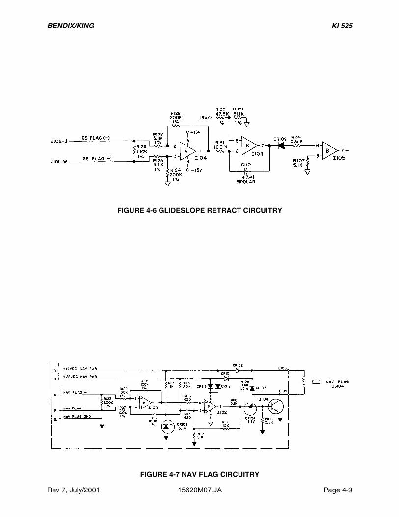
4.3.2 GS RETRACT CIRCUIT (Figure 4-6)
As the glideslope signal becomes weaker, the valid signal at bottom connector pin J and top con-nector pin W begins to decrease. This valid signal from the glideslope receiver is connected to resistors R126, R127 and R125 which represent a 1000ohm load to the receiver. Amplifier 1104A increases the amplitude of the valid signal by approximately forty and drives a level sensing circuit consisting of resistors R129, R130, R131; capacitor C110 and amplifier I104B. Capacitor C110 provides negative rate feedback to cause the circuit to operate as an integrator when the output of I104A becomes more positive than the switching point of I104B. The switching level is estab-lished by resistors R129 and E130 at approximately -7. 8VDC. When reduced by a factor of forty, this switching level corresponds to a level of 0. 195VDC at the glideslope receiver. Since amplifier I104A uses negative feedback, the output of this stage is negative, thus requiring the negative bias voltage on amplifier I104B. When the output of I104A exceeds -7. 8VDC, amplifier I104B slowly changes state from +15VDC to -15VDC. While amplifier I104B is in the -15VDC condition, the glideslope receiver is invalid resulting in current flow through forward biased diode CR109 and re-sistor R134. This negative current will overwhelm any current through resistor R162 or R166 re-sulting from the photocell or command signal and cause amplifier I105B to saturate at +15VDC. This voltage will cause amplifier I105A to saturate at -15VDC and force transistor Q109 to shut off and allow the glideslope pointer to deflect up and out of view.As the glideslope valid voltage exceeds 0. 195VDC, amplifier 1104B will slowly switch to +15VDC causing diode CR109 to be reversed biased, preventing current from flowing through resistor R 134. In this configuration, the glideslope pointer will drop into view and conform to the glideslope deviation command signal.

BENDIX/KING KI 525
Rev 7, July/2001 15620M07.JA Page 4-5
FIGURE 4-4 GLIDESLOPE DEVIATION SERVO LOOP

BENDIX/KING KI 525
Page 4-6 15620M07.JA Rev 7, July/2001
THIS PAGE IS RESERVED

BENDIX/KING KI 525
Rev 7, July/2001 15620M07.JA Page 4-7
FIGURE 4-5 GLIDESLOPE POSITION FEEDBACK SENSOR
BENDIX/KING KI 525
Rev 7, July/2001 15620M07.JA Page 4-9
FIGURE 4-6 GLIDESLOPE RETRACT CIRCUITRY
FIGURE 4-7 NAV FLAG CIRCUITRY

BENDIX/KING KI 525
Page 4-10 15620M07.JA Rev 7, July/2001
4.4 NAV FLAG CIRCUIT (Figure 4-7)The NAV valid signal originating at the VOR/LOC receiver is connected to pins K and F of the up-per P. C. board. Resistor R123 provides a 1Kohm load to the receiver. This signal then passes through resistors R121 and R122 to differential amplifier 1102A. Negative feedback is provided by resistor R117 which also established a gain of ONE for the stage. Since the amplifier is powered by a single ended power supply, i.e., +28VDC or ±14VDC to ground, the summing junctions at pins 2 and 3 of 1102A must be biased positive with respect to ground in order for the op-amp to function. This bias voltage is developed across zener diode CR108 in series with resistor R114 when using +28VDC power, and in series with resistor R115 when using +14VDC power. This +5. 1VDC bias voltage is connected to pin 3 of 1102A through resistor R118 and thus causes the out-put at pin 1 to stabilize at +5.1VDC also.The FLAG input voltage level from the NAV receiver will be inverted by 1102A and will appear at pin I in direct proportion to the input voltage change. From pin 1, the signal passes through resistor R116 to pin 6 of I102B. This signal is compared to the bias reference on pin 5 of I102B generated by zener diode CR108. During the NAV invalid condition the input voltage is near zero and the output from 1102A pin 1 is nearly 5. IVDC. The voltage at pin 5 of I102B, however, is less than 5. 1VDC because of the voltage divider consisting of resistors R112 and R113. This causes the volt-age to + pin 7 of I102B to switch to ground potential, removing the drive to transistor Q104 and providing a small amount of positive feedback to pin 5 of I102B through resistors R110 and Rl1l.When the input voltage increases to approximately +0. 21VDC, the output of I102A will decrease to +4. 9VDC which is less than the reference voltage on pin 5. This will cause amplifier 1102B to switch from near ground potential to +14VDC or +28VDC depending upon the power supply mag-nitude. Zener diode CR104 prevents transistor Q104 from turning on when 1102B is low since the output of this stage may be as high as one or two volts. When 1102B switches high, CR104 breaks down in the reverse direction, providing base current for Q104. This results in collector current through the NAV flag coil in series with CRI02 for 14VDC operation and R109 and CRlC1 for 28VDC operation. As the current builds up in the NAV flag coil, the small circular magnet between the coil poles rotates, causing the NAV flag to move up and out of view behind the front bezel.
4.5 POWER FLAGThe power flag operates in the same manner as the NAV flag, in that current flowing through the coil generates a magnetic field opposing the field in the circular magnet to which the flag is at-tached. This opposition causes the magnet to rotate and position the PWR flag out of view behind the front bezel. When the +15V unregulated supply from the KG 102 gyro drops below 2. OVDC, the attraction of the circular magnet poles to the pole pieces becomes greater than the repulsion force of the coil generated field-and results in a rapid rotation of the circular magnet to align with the pole pieces. This results in the reappearance of the PWR flag from behind the upper bezel.
4.6 HEADING SELECT AND COURSE DATUM PICKOFF ASSEMBLIESDual photo detectors V102 and V103 (figure 4-8) provide the DC outputs that correspond to the heading select and course datum signals respectively. A light beam from LED CRI15 illuminates V102, and CR111 illuminates V103. These light beams are partially interrupted by a shutter that rides on the heading select, or course datum cam attached to the center yoke assembly. (Figure 4-8). The horizontal slit in the shutter allows a narrow beam of light to fall on the photocell. This light causes a decrease in resistance of the photocell elements, but if both segments are equally exposed as shown in Figure 4-8B, the output voltage when measured against the mid point of re-sistor combination R135 and R136, will be zero. Resistors R135 and R136 provide the reference point for both pickoffs and prevents power supply variations from affecting the output voltage.

BENDIX/KING KI 525
Rev 7, July/2001 15620M07.JA Page 4-11
As the heading bug or course pointer is rotated clockwise, the shutter moves upward in response to the increasing cam radius. This results in greater exposure of the upper half of the dual photo-cell as shown in Figure 4-8A. A reduction in the resistance of this half unbalances the voltage di-vider and produces a positive output voltage between the photocell center top and the junction of resistors R 135 and R 136. As the heading bug or course pointer is rotated counterclockwise, the shutter moves downward, exposing the bottom half of the photocell. (figure 4-8). This results in a negative output voltage between the photocell center top and the junction of resistors R 135 and R 136.Rotation of the heading select bug will produce a continuously changing voltage within plus or mi-nus 30 degrees of the upper lubber line. Beyond that point, the voltage will remain constant at ap-proximately ± 12. 5VDC. When the bug is rotated to the bottom of the instrument, the voltage changes polarity and again remains constant until it is moved within 30 degrees of the upper lub-ber line where it begins to decrease toward zero volts.The course datum cam is cut in a similar fashion, except that it is symmetrical on the upper and lower sections allowing for back course autopilot operation. In addition, the course cam has a larg-er linear range than the heading cam, extending out to 80 degrees on either side of the upper or lower lubber lines with only 20 degrees of constant radius on each side of the instrument.
4.7 NAV DEVIATION AND TO-FROM INDICATORSUnlike the glideslope pointer, the NAV deviation and TO-FROM indicators are conventional meter movements mounted inside the center yoke assembly. The NAV meter is a 1000n, 15011a unit and the TO-FROM meter is a 200n, 200pa device.Drive current is supplied by the NAV receiver through P. C. board pins b and V for the NAV meter, and pins Z and T for the TO-FROM meter. From the P. C. board, the current passes through two pairs of brushes attached to the P. C. board that extended down on each side of four metal rings surrounding the.center yoke assembly as shown in Figure 4-9. Wires soldered to the four rings supply current to the respective meter movements.

BENDIX/KING KI 525
Page 4-12 15620M07.JA Rev 7, July/2001
THIS PAGE IS RESERVED

BENDIX/KING KI 525
Rev 7, July/2001 15620M07.JA Page 4-13
FIGURE 4-8 COURSE DATUM PICKOFF ASSEMBLY

BENDIX/KING KI 525
Rev 7, July/2001 15620M07.JA Page 4-15
FIGURE 4-9 CENTER YOKE WITH NAV AND TO-FROM BRUSH ASSEMBLY

BENDIX/KING KI 525
Page 4-16 15620M07.JA Rev 7, July/2001
THIS PAGE IS RESERVED

BENDIX/KING KI 525
Rev 7, July/2001 15620M07.JA Page 5-1
SECTION VMAINTENANCE
5.1 INTRODUCTION This section deals with the testing, overhaul, and trouble shooting procedure for the KI 525 Picto-rial Navigation Indicator.
5.2 TEST AND ALIGNMENT
5.2.1 GENERAL REQUIREMENTS
Unless otherwise specified all tests shall be conducted with the indicator in its normal operating position and at ambient room temperature (25 ±5 degrees C) and humidity not to exceed 80%.
5.2.1.1 ELECTRICAL
Output signalsa) HDG SEL 0.5 vdc/degb) CRS Datum 0.2 vdc/deg
Input signalsa) VOR deviation 15 mv/degb) GS deviation 300 mv/degc) VOR Flag valid 210 mvd) GS Valid 210 mve) PWR Valid 15 vdcf) TO-FROM ± 150 mvg) Lighting ± 14 vdc or +28 vdch) Two phase state signal to stepper motor
5.2.1.2 MECHANICAL
a) Compass Card 1/4 deg incrementsb) HDG Sel Cam 0.0016 in/degc) CRS DTM Cam 0.0006 in/deg
5.2.2 TEST EQUIPMENT
a) KTS-153 Test Setb) Precise angle indicator.c) ORZ test circuit described in RTCA 209-54/DD-62d) DC voltmeter-Similar to Fluke Model 8000Ae) Oscilloscope-Similar to Tektronix, Model 516.

BENDIX/KING KI 525
Page 5-2 15620M07.JA Rev 7, July/2001
5.2.3 CALIBRATION PROCEDURE
The initial phase of this procedure shall be performed with the unit in the final stage of assembly. The PC board shall be wired to the harness but not assembled to the main structural casting.
1) Place the KTS-153 Power Switch OFF. Connect the unit to the tester. Connect a precise angle indicator (PAI) to the HDG CX jacks on the front of the tester.
2) Carefully rotate the first gear forward of the slip rings until NORTH is precisely un-der the lubber line. Loosen the heading repeater hold-down screws, and rotate the synchro for 0.00° on the PAI. Tighten the hold-down screws.
3) Rotate the heading card until EAST appears under the lubber line. The PAI shall read 90 ±1.0°.
4) Return the heading card to 0.0°, and loosen the slaving CT hold-down screws. Switch the PAI to the slaving CT, and rotate the synchro for 0.00° on the PAI. Tight-en the hold-down screws.
5) Rotate the heading card until EAST appears under the lubber line. The PAI shall read 90 ±1.0°.
6) Rotate the heading card to NORTH, and position the course pointer at 300°. Con-nect the ORZ test set to the OBS Resolver jacks. Loosen the course resolver hold-down screws and calibrate the 30 Hz resolver according to the constant rotor volt-age test procedures given in RTCA paper 209-54/DO-62. Tighten the hold-down screws. Assemble the PC board to the main structure but do not install the unit cover.
7) Place the following tester switches to the indicated position:SWITCH POSITIONRES/DEV DEVD-BAR/TO-FM D-BARMETER GS DEV14/28 vdc +14 vdc on Panel Meter±15 vdc ON+5 vdc ONGS DEV CMR OFFGS FLAG CMR OFFCCW-CW CCWStepper Drive OFFNAV FLAG CMR OFF+15 VNREG NORMAL115 VAC 400 Hz. ON
8) Adjust the 14/28 vdc pot for 28 vdc on the tester voltmeter.9) Place a black cloth over the indicator to remove as much light as possible from the
three photocell areas. Adjust the GS flag pot fully clockwise, and the GS DEV pot for 0.0 vdc E(+) to B(-)(J2). Refer to figure 5-1 and loosen the GS photocell assem-bly hold down screw. Carefully adjust the photocell assembly to position the glides-lope pointer directly over the center mark on the glideslope scale when viewing the indicator from 25 degrees above the front. Tighten the photocell assembly hold-down screw.
BENDIX/KING KI 525
Rev 7, July/2001 15620M07.JA Page 5-3
10) Adjust the GS DEV pot fully clockwise. The GS pointer shall move toward the top of the indicator. Adjust pot R147 until the GS pointer is just in view at the top of the indicator when viewed from 30° above the longitudinal axis of the unit. Adjust the GS DEV pot for 0.0Vdc.
11) Position the heading bug and the course pointer precisely under the lubber line. Loosen the two shutter hold-down screws on each shutter less than 1/2 turn.
12) Monitor the voltage from P(+) to S(-) (J1). With the black cloth covering the unit, move the heading shutter (forward photocell) with the adjusting tool until the volt-age P(+) to S(-) (J1) is 0.0Vdc. Carefully tighten the two hold-down screws while maintaining 0.0Vdc from P(+) to S(-).
13) Monitor the voltage from pin e (+) to S(-) (J1). Repeat the above adjustment pro-cedure on the CRS shutter (rearward).
14) Position the HDG bug to 10 ±0.5° to the right of the lubber line and the CRS Pointer to 10 ±0.5° to the left of the lubber line. Adjust R169 for +5.5Vdc from pin P(+) to S(-) (J1) and adjust R170 for -2.1 vdc from pin e (+) to S(-) (J1).
15) Remove all power from the unit. Apply glyptal to the four shutter hold-down screws and to the GS photocell assembly hold-down screw. Place the cover on the unit, and secure it with two rear-mounted screws.
5.2.4 FINAL TEST PROCEDURE
The unit shall be completely assembled with the cover in place. 1) Connect the unit to the tester, and set the panel switches as listed in 5.2.3 (7)
above. Place the heading and course pointers under the lubber line, and adjust the GS flag, GS deviation, and NAV flag sources for 0.0 Vdc. Record the following volt-ages:a) J1 Pin P(+) to S(-) 0.0±0.3Vdc b) J1 Pin e(+) to S(-) 0.0±0.60Vdc
2) Adjust the 14/28 Vdc pot for +11.2 Vdc on the panel meter. The NAV and PWR flags shall be fully in view. Slowly increase the NAV flag voltage until the NAV flag snaps up out of view. The flag shall be completely out of view.NAV flag voltage K(+) to F(-) +0.21 ±0.03Vdc. Adjust the 14/28 VDC pot for +14.0Vdc.
3) Switch the NAV flag CMR switch to the POS position. Re-adjust the NAV flag volt-age to the value recorded in 2 above. The NAV flag shall not be in view.
4) Switch the 14/28V NAV PWR OFF. The NAV flag shall come completely into view. 5) Switch the 14/28V NAV PWR to the 28V position, and adjust the 14/28 VDC pot for
+28.0Vdc. The NAV flag shall go completely out of view. 6) Decrease the voltage to 22.4Vdc. The NAV flag shall remain out of view. 7) Slowly decrease the NAV flag voltage until the NAV flag drops into view. The NAV
flag voltage K(+) to F(-) shall be 0.17 ±0.03Vdc. Return the input voltage to +28Vdc.
8) Monitor the voltage on P(+) to S(-) and adjust the heading pointer 10° left of the lubber line.P(+) to S(-) -5.5 ±1.2Vdc
9) Continue to rotate the heading pointer to the left until the voltage stops changing. The pointer shall be 30 ±5° right of the lubber line.P(+) to S(-) -12.5 ±2Vdc

BENDIX/KING KI 525
Page 5-4 15620M07.JA Rev 7, July/2001
10) Adjust the pointer 10° right of the lubber line.P(+) to S(-) +5.5 ±1.2Vdc (Offset recorded in 1)a) shall be used as the reference for this measurement.)
11) Continue to rotate the heading pointer to the right until the voltage stops changing. The pointer shall be 30 ±5° right of the lubber line. P(+) to S(-) +12.5 ±2VVdc
12) Continue rotating the heading pointer to the right until the voltage switches to -14±3Vdc. The heading pointer shall be within 10° of the bottom of the indicator.
13) Monitor the voltage J1 e(+) to S(-), and adjust the course pointer 10° left. e(+) to S(-) -2.1±0.4Vdc
14) Continue to rotate the course pointer to the left until the voltage stops changing. The pointer shall be 80±10° left of the lubber line. e(+) to S(-) -12.5±2Vdc
15) Adjust the course pointer 10° right of the lubber line.e(+) to S(-) +2.1 ±0.4Vdc
16) Continue to rotate the course pointer to the right until the voltage stops changing. The pointer shall be 80±10 degrees right of the lubber line. e(+) to S(-) +12.5±2Vdc
17) Continue to rotate the course pointer to the right until the voltage begins to de-crease.CRS pointer 100 ±10 deg. right of the lubber line
18) Continue the right hand rotation until the voltage reads 0.0 vdc. The course pointer shall be within 10 degrees of the bottom of the indicator.
19) Continue the right hand rotation until the voltage stops changing.CRS pointer 100 ±10 deg. left of the lubber line
20) Adjust the GS deviation for maximum positive, maximum negative, and then back to zero. At no time shall the GS pointer come into view.
21) Increase the GS flag voltage J2-J(+) to J1-W(-) to 0.215Vdc.a) The GS pointer shall drop into view within 10 seconds. b) GS pointer center scale ±1/2 needle width (left side).c) GS pointer center scale ±1/2 needle width (right side). d) The GS pointer shall have no tendency to oscillate.
22) Switch the GS flag CMR switch to the POS, NEG, and then OFF positions. At no time shall the GS pointer move out of view.
23) Adjust the GS pointer to the following positions on the GS scale, and record the input voltages from E to B (J2). a) One dot up +75 ±10mVdcc) Two dots up +150 ±20mVdcd) Maximum up command Pointer in view at top of scale
when viewed at 30° above unit centerline
e) One dot down -75 ±10mVdcf) Two dots down -150 ±20mVdc
24) Adjust the GS flag voltage, (J2-J to J1-W), to 0.185Vdc. The GS pointer shall slow-ly move up out of view.

BENDIX/KING KI 525
Rev 7, July/2001 15620M07.JA Page 5-5
25) Adjust the GS DEV voltage to 0.0Vdc. 26) Place the RES/DEV switch to RES, and the DEV-BAR/TO-FROM switch to DEV-
BAR. Adjust the RES pot for 0.3Vdc at TP-A. (J1) Pin b 0.150±0.004Vdc
27) Switch the DEV-BAR TO-FROM switch to the TO-FROM position, and adjust the RES pot for 0.3Vdc at TP-A. Pin Z 0.050±0.005Vdc
28) Switch the RES/DEV switch to DEV, and rotate the METER CURRENT adjust for a fully in-view TO indication. Position the course pointer under the lubber line. (TO-FROM flag points toward course pointer.) J1 Z(+) to T(-) +200±40 (adc
29) Repeat for a full FROM indication. J1 Z(+) to T(-) -200±40 (adc
30) Rotate the Meter Current adjust to 0.0. Slowly rotate the course pointer 360°. The TO-FROM flag shall remain totally out of view when viewed from the front.
31) Tilt the unit 90° up. The TO-FROM flag shall remain out of view. 32) Switch the DEV-BAR TO-FROM switch to the DEV-BAR position, and position the
course pointer under the lubber line. With the Meter Current adjust at 0.0Vdc, the course deviation bar shall be aligned with the ends of the course select pointer and the symbolic airplane centerline within 1/4 bar width.
33) Slowly rotate the course pointer 360°. The DEV bar shall not move more than 1/2 bar width.
34) Tilt the unit 90° up. The DEV bar shall not move more than 1/2 bar width. 35) Adjust the DEV bar to the following positions. Record the current readings on the
panel Microamp Meter. The movement of the DEV bar shall be unrestricted throughout the travel.a) One dot left -30±4 (adc b) Two dots left -60±8 (adc c) Three dots left -90±12 (adc d) Four dots left -120±16 (adc e) Five dots left -150±20 (adc f) Five dots right +150±20 (adc g) Four dots right +120±16 (adc h) Three dots right +90±12 (adc i) Two dots right +60±8 (adc j) One dot right +30±4 (adc
36) Switch the stepper drive ON, and adjust the slew speed for a 1.0-second square wave period at Pin A (J2). The heading card shall move smoothly with uniform steps. Switch the CW/CCW switch to CW, and check for smoothness.
37) Decrease the square wave period at Pin A (J2) to 67ms, and check the display for smoothness in both directions.
38) Switch the stepper drive off, and position the heading bug to 360°, and the course pointer at 90° relative to the compass card. Switch the stepper drive on, and allow the card to make two revolutions. The heading bug and the course pointer shall be within two degrees of the respective starting positions. Repeat this test with the display rotating in the opposite direction.

BENDIX/KING KI 525
Page 5-6 15620M07.JA Rev 7, July/2001
39) Rotate the heading knob in a direction opposite to that of the compass card. The compass card shall continue rotating smoothly without missing any steps. Repeat for the opposite direction. Allow the compass cards to rotate 360° in each direction.
40) Decrease the square wave period at Pin A (J2) to 33ms, and check the display for smoothness in both directions. There shall be no evidence of missed steps. In-crease the square wave period to 0.1 second, and shut off the display.
41) Connect the PAI to the panel jacks shown, and position NORTH under the lubber line using the stepper drive direction and speed control. a) PAI: Slaving CT 0.0±1.0°b) PAI: HDG CX 0.0±1.0°Position the compass card to the headings shown, and record the PAI values. c) HDG: 90° Slave CT 90±1.0°
HDG CX 90±1.0°d) HDG: 180° Slave CT 180±1.0°
HDG CX 180±1.0°e) HDG: 270° Slave CT 270±1.0°
HDG CX 270±1.0°f) HDG: 0.0° Slave CT 0±1.0°
HDG CX 0±1.0°42) The course resolver shall be zeroed at 300° ±1° using the constant rotor voltage
test in RTCA paper 209-54/DO-62. 43) The stator output voltages determined in accordance with the constant rotor volt-
age test shall be 0.180 ±0.012. 44) Connect the resolver to a calibrated resolver, phase shifter, accuracy bridge, or
equivalent error-measuring equipment, and excite the rotor with 0.5V 30Hz. Rotate the course knob clockwise to position the course pointer at 60° increments from 0° to 360°. The maximum error shall be ±1°.
45) Switch the +15 unregulated switch to VARIABLE, and rotate the adjust pot fully counter-clockwise. The PWR flag shall be fully in view.
46) Slowly rotate the adjust pot clockwise until the PWR flag snaps out of view.Pin v (J101) +10 +3/-4Vdc
47) Slowly rotate the pot counter-clockwise until the PWR flag snaps into view.Pin v (J101) +4 ±3Vdc
48) Place the +15 unregulated switch to NORMAL.49) Adjust the lighting pot fully CW and observe both lamps on and uniform illumination
of the display.50) Switch the 14/28v switch to l4v and adjust for 14vdc on the panel Meter. Both lamps
shall be on and the display shall be illuminated in a uniform manner.51) Slowly decrease the lighting intensity. The display illumination shall decrease in a
smooth and uniform fashion.52) Switch the 14/28v switch to 28v and adjust for 28vdc on the panel meter. Slowly
increase the lighting intensity. The display illumination shall increase in a smooth and uniform manner.
53) Adjust the METER CURRENT pot for half-scale on the DEV-BAR, and slowly ro-tate the compass card 360° using the stepper drive controls. There shall be no dis-continuity in the DEV-BAR display.
BENDIX/KING KI 525
Rev 7, July/2001 15620M07.JA Page 5-7
54) Place the DEV-BAR/TO-FROM switch to TO-FROM, and adjust the METER CUR-RENT pot until the flag is just off the stop in either the TO or FROM position. Slowly rotate the compass card 360°. There shall be no discontinuity in the TO-FROM dis-play.
55) Rotate the METER CURRENT pot fully clockwise. Reduce the current to 100 uadc. The TO-FROM flag shall move smoothly off the stop. Repeat for the oppo-site polarity.
56) Place the DEV-BAR/TO-FROM switch to the DEV-BAR position, and rotate the METER CURRENT pot fully clockwise. Rotate the compass card 360°. The D-bar shall not touch the compass card. Reduce the current to 90 uadc. The D-bar shall move smoothly off the stop. Repeat for the opposite polarity.

BENDIX/KING KI 525
Page 5-8 15620M07.JA Rev 7, July/2001
THIS PAGE IS RESERVED

BENDIX/KING KI 525
Rev 7, July/2001 15620M07.JA Page 5-9
TEST DATA SHEETS
1) CRS AND HDG under lubber linea) J1 Pin P to S(-) _____________ 0.0 +/-0.3 vdcb) Jl Pin e to S(-) _____________ 0.0 +/-0.6 vdc
2) Input voltage to 11.2vdcNAV flag out of viewJ1K to P(-) _____________ 0.21 +/-0.03 vdc
3) NAV flag CMR to PosNAV flag _____________ out of view
4) 14/28 vdc OFFNAV flag _____________ IN VIEW
5) 28v input powerNAV flag _____________ out of view
6) Input voltage to 22.4 vdcNAV flag _____________ out of view
7) NAV thresholdNAV flag in viewJ1K to F(-) _____________ -0.17+/-0.03vdcPWR VALIDPWR flag _____________ Out of view
8) HDG SEL 10 deg LeftJ1P to S(-) _____________ -5.5 +/-1.2 vdc
9) HDG SEL to limit leftJ1P to S(-) _____________ -12.5 +/-2 vdc
10) HDG SEL 10 deg RightJ1P to S(-) _____________ +5.5 +/-1.2 vdc
11) HDG SEL to limit Right _____________ 30 +/-5 deg RightJ1P to S(-) _____________ +12.5 +/-2 vdc
12) HDG SEL Rightto Crossover _____________ bottom +/- 10 deg
13) CRS 10 deg LeftJ1e to S(-) _____________ -2.1 +/-0.4 vdc
14) CRS to limit left _____________ -2.1 +/-0.4 vdcJ1e to S(-) _____________ 12.5 +/-2 vdc
15) CRS 10 deg RightJ1e to S(-) _____________ +2.1 +/-0.4vdc
16) CRS to limit Right _____________ 80 +/-10 deg RightJ1e to S(-) _____________ +12.5 +/-2vdc
17) End of CRS limit Right _____________ 100 +/-10 deg Right
18) CRS Null at bottom _____________ bottom +/-10 deg
19) End of CRS limit left _____________ 100 +/-10 deg left
20) GS Max Pos, Neg, Zero _____________ Out of view
BENDIX/KING KI 525
Page 5-10 15620M07.JA Rev 7, July/2001
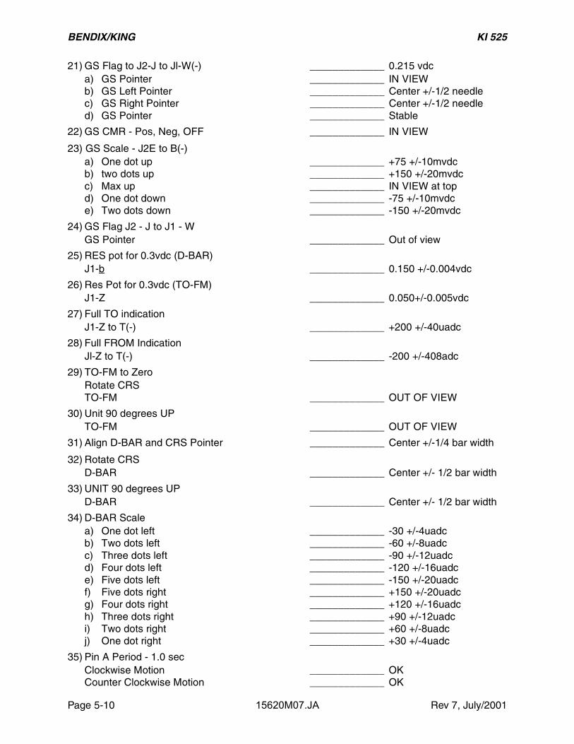
21) GS Flag to J2-J to Jl-W(-) _____________ 0.215 vdca) GS Pointer _____________ IN VIEWb) GS Left Pointer _____________ Center +/-1/2 needlec) GS Right Pointer _____________ Center +/-1/2 needled) GS Pointer _____________ Stable
22) GS CMR - Pos, Neg, OFF _____________ IN VIEW
23) GS Scale - J2E to B(-)a) One dot up _____________ +75 +/-10mvdcb) two dots up _____________ +150 +/-20mvdcc) Max up _____________ IN VIEW at topd) One dot down _____________ -75 +/-10mvdce) Two dots down _____________ -150 +/-20mvdc
24) GS Flag J2 - J to J1 - WGS Pointer _____________ Out of view
25) RES pot for 0.3vdc (D-BAR)J1-b _____________ 0.150 +/-0.004vdc
26) Res Pot for 0.3vdc (TO-FM)J1-Z _____________ 0.050+/-0.005vdc
27) Full TO indicationJ1-Z to T(-) _____________ +200 +/-40uadc
28) Full FROM IndicationJl-Z to T(-) _____________ -200 +/-408adc
29) TO-FM to ZeroRotate CRSTO-FM _____________ OUT OF VIEW
30) Unit 90 degrees UPTO-FM _____________ OUT OF VIEW
31) Align D-BAR and CRS Pointer _____________ Center +/-1/4 bar width
32) Rotate CRSD-BAR _____________ Center +/- 1/2 bar width
33) UNIT 90 degrees UPD-BAR _____________ Center +/- 1/2 bar width
34) D-BAR Scalea) One dot left _____________ -30 +/-4uadcb) Two dots left _____________ -60 +/-8uadcc) Three dots left _____________ -90 +/-12uadcd) Four dots left _____________ -120 +/-16uadce) Five dots left _____________ -150 +/-20uadcf) Five dots right _____________ +150 +/-20uadcg) Four dots right _____________ +120 +/-16uadch) Three dots right _____________ +90 +/-12uadci) Two dots right _____________ +60 +/-8uadcj) One dot right _____________ +30 +/-4uadc
35) Pin A Period - 1.0 secClockwise Motion _____________ OKCounter Clockwise Motion _____________ OK

BENDIX/KING KI 525
Rev 7, July/2001 15620M07.JA Page 5-11
36) Pin A Period - 67 msCW Motion _____________ OKCCW Motion _____________ OK
37) HDG bug at 360 degreesCRS at 90 degreesTwo RevolutionsHDG bug _____________ 360 +/-2degCRS _____________ 90 +/-2 deg
Reverse DirectionHDG bug _____________ 360 +/-2degCRS _____________ 90 +/-2-deg
38) HDG bug opposite of CardCompass Card _____________ No missed pulses
Opposite directionCompass Card _____________ no missed pulses
39) Pin A period - 33 Ms.Compass Card _____________ No missed pulses
Pin A period 0.1 second DISPLAY OFF
40) PAI check - N under lubber linea) Slaving CT _____________ 0.0 +/-1.0 degb) HDG CX _____________ 0.0 +/-1.0 deg
Compass Checka) HDG - 90 deg
Slave CT _____________ 90 +/-1.0 degHDG CX _____________ 90 +/-1.0 deg
b) HDG - 180 degSalve CT _____________ 180 +/-1.0 degHDG CX _____________ 180 +/-1.0 deg
c) HDG - 270 deg.Slave CT _____________ 270 +/-1.0 degHDG CX _____________ 270 +/-1.0 deg
d) HDG - 0.0 degSlave CT _____________ 0.0 +/-1.0 degHDG CX _____________ 0.0 +/-1. 0deg
41) CRS Resolver _____________ OK
42) Stator Output Voltage _____________ 0.180 +/-0.012 VAC
43) CRS Resolver AccuracyCRS - 0.0 deg _____________ 0.0 +/-1 deg
60 deg _____________ 60 +/-1 deg 120 deg _____________ 120 +/-1 deg 180 deg _____________ 180 +/-1 deg 240 deg _____________ 240 +/-1 deg 300 deg _____________ 300 +/-1 deg
44) 15 volt unreg fully CCWPWR Flag _____________ IN VIEW
45) PWR Flag out of viewJl-Pin v _____________ +10 +3/-4 vdc

BENDIX/KING KI 525
Page 5-12 15620M07.JA Rev 7, July/2001
46) PWR Flag in viewJI-Pin v _____________ +4 +/-3vdc
47) PWR INVALIDPWR Flag _____________ IN VIEW
48) Lighting _____________ OK
49) Lighting to l4v _____________ OK
50) Variable LightingIntensity _____________ OK
51) Lighting to 28V _____________ OK
52) D-BAR Continuity _____________ OK
53) TO-FM Continuity _____________ OK
54) TO-FM Stops _____________ OKOpposite polarity _____________ OK
55) D-BAR Interference _____________ OKD-BAR Stops _____________ OKOpposite polarity _____________ OK

BENDIX/KING KI 525
Rev 7, July/2001 15620M07.JA Page 5-13
FIGURE 5-1 Glideslope Assembly Calibration

BENDIX/KING KI 525
Page 5-14 15620M07.JA Rev 7, July/2001
THIS PAGE IS RESERVED

BENDIX/KING KI 525
Rev 7, July/2001 15620M07.JA Page 5-15
5.3 OVERHAUL
5.3.1 VISUAL INSPECTION
This section contains instructions and information to assist in determining, by visual inspection, the condition of the units major assemblies and subassemblies. These inspection procedures will assist in finding defects resulting from wear, physical damage, deterioration, or other causes. To aid inspection, detailed procedures are arranged in alphabetical order.
A. Capacitors, FixedInspect capacitors for case damage, body damage, and cracked, broken, or charred insulation. Check for loose, broken, or corroded terminal studs, lugs, or leads. Inspect for loose, broken, or improperly soldered connections. On chip caps, be especially alert for hairline cracks in the body and broken terminations.
B. Capacitors, VariableInspect trimmers for chipped and cracked bodies, damaged dielectrics, and dam-aged contacts.
C. ChassisInspect the chassis for loose or missing mounting hardware, deformation, dents, damaged fasteners, or damaged connectors. In addition, check for corrosion or damage to the finish that should be repaired.
D. Circuit BoardsInspect for loose, broken, or corroded terminal connections; insufficient solder or improper bonding; fungus, mold, or other deposits; and damage such as cracks, burns, or charred traces.
E. ConnectorsInspect the connector bodies for broken parts; check the insulation for cracks, and check the contacts for damage, misalignment, corrosion, or bad plating. Check for broken, loose, or poorly soldered connections to terminals of the connectors. In-spect connector hoods and cable clamps for crimped wires.
F. Covers and ShieldsInspect covers and shields for punctures, deep dents, and badly worn surfaces. Al-so, check for damaged fastener devices, corrosion and damage to finish.
G. Flex CircuitsInspect flex circuits for punctures, and badly worn surfaces. Check for broken trac-es, especially near the solder contact points.
H. Front PanelCheck that name, serial, and any plates or stickers are secure and hardware is tight. Check that the handle is functional, securely fastened, and handle casting is not damaged or bent.
I. FuseInspect for blown fuse and check for loose solder joints.
J. InsulatorsInspect insulators for evidence of damage, such as broken or chipped edges, burned areas, and presence of foreign matter.
K. JacksInspect all jacks for corrosion, rust, deformations, loose or broken parts, cracked insulation, bad contacts, or other irregularities.

BENDIX/KING KI 525
Page 5-16 15620M07.JA Rev 7, July/2001
L. PotentiometersInspect all potentiometers for evidence of damage or loose terminals, cracked in-sulation or other irregularities.
M. Resistors, FixedInspect the fixed resistors for cracked, broken, blistered, or charred bodies and loose, broken, or improperly soldered connections. On chip resistors, be especially alert for hairline cracks in the body and broken terminations.
N. RF CoilsInspect all RF coils for broken leads, loose mountings, and loose, improperly sol-dered, or broken terminal connections. Check for crushed, scratched, cut or charred windings. Inspect the windings, leads, terminals and connections for cor-rosion or physical damage. Check for physical damage to forms and tuning slug adjustment screws.
O. Terminal Connections Soldered(1) Inspect for cold-soldered or resin joints. These joints present a po-
rous or dull, rough appearance. Check for strength of bond using the points of a tool.
(2) Examine the terminals for excess solder, protrusions from the joint, pieces adhering to adjacent insulation, and particles lodged be-tween joints, conductors, or other components.
(3) Inspect for insufficient solder and unsoldered strands of wire pro-truding from the conductor at the terminal. Check for insulation that is stripped back too far from the terminal.
(4) Inspect for corrosion at the terminal.P. Transformers
(1) Inspect for signs of excessive heating, physical damage to the case, cracked or broken insulation, and other abnormal conditions.
(2) Inspect for corroded, poorly soldered, or loose connecting leads or terminals.
Q. Wiring/Coaxial CableInspect wiring in chassis for breaks in insulation, conductor breaks, cut or broken lacing and improper dress in relation to adjacent wiring or chassis.
5.3.2 CLEANING
A. GeneralThis section contains information to aid in the cleaning of the component parts and subassemblies of the unit.
WARNING:GOGGLES ARE TO BE WORN WHEN USINGPRESSURIZED AIR TO BLOW DUST ANDDIRT FROM EQUIPMENT. ALL PERSONNELSHOULD BE WARNED AWAY FROM THE IM-MEDIATE AREA.

BENDIX/KING KI 525
Rev 7, July/2001 15620M07.JA Page 5-17
WARNING:OPERATIONS INVOLVING THE USE OF ACLEANING SOLVENT SHOULD BE PER-FORMED UNDER A VENTILATED HOOD.AVOID BREATHING SOLVENT VAPOR ANDFUMES; AVOID CONTINUOUS CONTACTWITH THE SOLVENT. WEAR A SUITABLEMASK, GOGGLES, GLOVES, AND AN APRONWHEN NECESSARY. CHANGE CLOTHINGUPON WHICH SOLVENTS HAVE BEENSPILLED.
WARNING:OBSERVE ALL FIRE PRECAUTIONS FORFLAMMABLE MATERIALS. USE FLAMMABLEMATERIALS IN A HOOD PROVIDED WITHSPARK-PROOF ELECTRICAL EQUIPMENTAND AN EXHAUST FAN WITH SPARKPROOFBLADES.
B. Recommended Cleaning AgentsTable 5-1 lists the recommended cleaning agents to be used during overhaul of the unit.
NOTE:EQUIVALENT SUBSTITUTES MAY BE USED FORLISTED CLEANING AGENTS.
TABLE 5-1 RECOMMENDED CLEANING AGENTS
C. Recommended Cleaning Procedures
TYPE USED TO CLEAN
Denatured Alcohol Various, exterior and interior
DuPont Vertrel SMT Various, interior
PolaClear Cleaner (Polaroid Corp.) or Texwipe TX129 (Texwipe Co.)
CRT display filter, LCD displays, and general purpose lens/glass cleaner.
KimWipes lint-free tissue(Kimberly Clark Corp.)
Various
Cloth, lint-free cotton Various
Brush, flat with fiber bristles Various
Brush, round with fiber bristles Various
Dishwashing liquid (mild) Nylon, Rubber Grommets

BENDIX/KING KI 525
Page 5-18 15620M07.JA Rev 7, July/2001
CAUTION:DO NOT ALLOW SOLVENT TO RUN INTOSLEEVES OR CONDUIT THAT COVERSWIRES CONNECTED TO INSERT TERMI-NALS.
1. Exterior(a) Wipe dust cover and front panel with a lint-free cloth dampened with
denatured alcohol.(b) For cleaning connectors, use the following procedure.
(1) Wipe dust and dirt from bodies, shells, and cable clamps using a lint-free cloth moistened with dena-tured alcohol.
(2) Wipe parts dry with a clean, dry lint-free cloth.(3) Remove dirt and lubricant from connector inserts, in-
sulation, and terminals using a small soft bristled brush moistened with denatured alcohol.
(4) Dry the inserts with an air jet.(c) Remove cover(s).(d) If necessary, open any blocked ventilation holes by first saturating
the debris clogging the apertures with denatured alcohol and then blowing the loosened material out with an air stream.
2. InteriorThe following solvents are no longer recommended for benchtop or rework cleaning of printed circuit boards, modules, or sub-assem-blies.
TABLE 5-2 UNSAFE CLEANING AGENTS
FREON TF, IMC TRICHLOROETHANE
CARBON TETRACHLORIDE DETERGENT (ALL AND EQUIVALENTS)
CHLOROFORM METHYLENE CHLORIDE
TRICHLOROETHYLENE GENESOLV 2004/2010
PROPYL ALCOHOL METHYL ALCOHOL
ETHYL ALCOHOL BUTYL ALCOHOL
XYLENE PRELETE (CFC-113)

BENDIX/KING KI 525
Rev 7, July/2001 15620M07.JA Page 5-19
CAUTION:DO NOT USE SOLVENT TO CLEAN PARTSCOMPOSED OF OR CONTAINING NYLON ORRUBBER GROMMETS. CLEAN THESEITEMS WITH MILD LIQUID DISHWASHINGDETERGENT AND WATER. USE DETER-GENT FOR THIS PURPOSE ONLY.
CAUTION:DUPONT VERTREL SMT DOES HAVE GEN-ERAL MATERIAL COMPATIBILITY PROB-LEMS WITH POLYCARBONATE, POLYSTY-RENE, AND RUBBER. IT IS RECOMMENDEDTHAT THESE MATERIALS BE CLEANEDWITH DENATURED ALCOHOL.
CAUTION:DO NOT ALLOW EXCESS CLEANING SOL-VENT TO ACCUMULATE IN ANY OF THE AD-JUSTMENT SCREW CREVICES AND THERE-BY SOFTEN OR DISSOLVE THE ADJUST-MENT SCREW EPOXY SEALANT.
CAUTION:AVOID AIR-BLASTING SMALL TUNING COILSAND OTHER DELICATE PARTS BY HOLDINGTHE AIR NOZZLE TOO CLOSE. USE BRUSH-ES CAREFULLY ON DELICATE PARTS.
CAUTION:IMPROPER CLEANING CAN RESULT IN SUR-FACE LEAKAGE AND CONDUCTIVE PARTIC-ULATES, SUCH AS SOLDER BALLS OR ME-TALLIC CHIPS, WHICH CAN CAUSE ELEC-TRICAL SHORTS. SEVERE IONIC CONTAM-INATION FROM HANDLING AND FROMENVIRONMENTAL CONDITIONS CAN RE-SULT IN HIGH RESISTANCE OR OPEN CIR-CUITS.
CAUTION:ULTRASONIC CLEANING CAN DAMAGECERTAIN PARTS AND SHOULD GENERALLYBE AVOIDED.

BENDIX/KING KI 525
Page 5-20 15620M07.JA Rev 7, July/2001
NOTE:Solvents may be physically applied in several waysincluding agitation, spraying, brushing, and vapordegreasing. The cleaning solvents and methodsused shall have no deleterious effect on the parts,connections, and materials being used. If sensitivecomponents are being used, spray is recommended.Uniformity of solvent spray flow should be maxi-mized and wait-time between soldering and cleaningshould be minimized.
NOTE:Clean each module subassembly. Then remove anyforeign matter from the casting.
Remove each module subassembly. Then remove any foreign mat-ter from the casting.(a) Casting covers and shields should be cleaned as follows:
(1) Remove surface grease with a lint-free cloth.(2) Blow dust from surfaces, holes, and recesses using
an air stream.(3) If necessary, use a solvent, and scrub until clean,
working over all surfaces and into all holes and re-cesses with a suitable non-metallic brush.
(4) Position the part to dry so the solvent is not trapped in holes or recesses. Use an air stream to blow out any trapped solvent.
(5) When thoroughly clean, touch up any minor damage to the finish.
(b) Assemblies containing resistors, capacitors, rf coils, inductors, transformers, and other wired parts should be cleaned as follows:
(1) Remove dust and dirt from all surfaces, including all parts and wiring, using soft-bristled brushes in con-junction with air stream.
(2) Any dirt that cannot be removed in this way should be removed with a brush (not synthetic) saturated with an approved solvent, such as mentioned above. Use of a clean, dry air stream (25 to 28 psi) is recom-mended to remove any excess solvent.
(3) Remove flux residue, metallic chips, and/or solder balls with an approved solvent.
(c) Wired chassic devices containing terminal boards, resistor and ca-pacitor assemblies, rf coils, switches, sockets, inductors, transform-ers, and other wired parts should be cleaned as follows:

BENDIX/KING KI 525
Rev 7, July/2001 15620M07.JA Page 5-21
NOTE:When necessary to disturb the dress of wires andcables, note the positions before disturbing and re-store them to proper dress after cleaning.
(1) Blow dust from surfaces, holes, and recesses using an air jet.
(2) Finish cleaning chassis by wiping finished surfaces with a lint-free cloth moistened with solvent.
(3) Dry with a clean, dry, lint-free cloth.(4) When thoroughly clean, touch-up any minor damage
to the finish.(5) Protect the chassis from dust, moisture, and damage
pending inspection.(d) Ceramic and plastic parts should be cleaned as follows:
(1) Blow dust from surfaces, holes, and recesses using an air jet.
(2) Finish cleaning chassis by wiping finished surfaces with a lint-free cloth moistened with solvents.
(3) Dry with a clean, dry, lint-free cloth.
5.3.3 REPAIR
A. GeneralThis section contains information required to perform limited repairs on the unit. The repair or replacement of damaged parts in airborne electronic equipment usu-ally involves standard service techniques. In most cases, examination of drawings and equipment reveals several approaches to perform a repair. However, certain repairs demand following an exact repair sequence to ensure proper operation of the equipment. After correcting a malfunction in any section of the unit, it is recom-mended that a repetition of the functional test of the unit be performed.
B. Repair Precautions1. Ensure that all ESDS and MOS handling precautions are followed.2. Perform repairs and replace components with power disconnected
from equipment.3. Use a conductive table top for repairs and connect table to ground
conductors of 60Hz and 400Hz power lines.4. Replace connectors, coaxial cables, shield conductors, and twisted
pairs only with identical items.5. Reference “component side” of a printed circuit board in this manual
means the side on which components are located; “solder side” re-fers to the other side. The standard references are as follows: near-side is the component side; farside is the solder side; on surface mount boards with components on both sides, the nearside is the side that has the J#### and P#### connector numbers.
6. When repairing circuits, carefully observe lead dress and compo-nent orientation. Keep leads as short as possible and observe cor-rect repair techniques.

BENDIX/KING KI 525
Page 5-22 15620M07.JA Rev 7, July/2001
7. There are certain soldering considerations with surface mount com-ponents. The soldering iron tip should not touch the ceramic com-ponent body. The iron should be applied only to the termination-sol-der filet.
8. Observe cable routing throughout instrument assembly, prior to dis-assembly, to enable a proper reinstallation of cabling during reas-sembly procedures.
CAUTIONTHIS EQUIPMENT CONTAINS ELECTRO-STATIC DISCHARGE SENSITIVE (ESDS) DE-VICES. EQUIPMENT MODULES AND ESDSDEVICES MUST BE HANDLED IN ACCOR-DANCE WITH SPECIAL ESDS HANDLINGPROCEDURES.
C. Electrostatic Sensitive Devices (ESDS) Protection1. Always discharge static before handling devices by touching some-
thing that is grounded.2. Use a wrist strap grounded through a 1MΩ resistor.3. Do not slide anything on the bench. Pick it up and set it down in-
stead.4. Keep all parts in protective cartons until ready to insert into the
board.5. Never touch the device leads or the circuit paths during assembly.6. Use a grounded tip, low wattage soldering station.7. Keep the humidity in the work environment as high as feasibly pos-
sible.8. Use grounded mats on the work station unless table tops are made
of approved antistatic material.9. Do not use synthetic carpet on the floor of the shop. If a shop is car-
peted, ensure that a grounded mat is placed at each workstation.10. Keep common plastics out of the work area.
D. MOS Device ProtectionMOS (Metal Oxide Semiconductor) devices are used in this equipment. While the attributes of MOS type devices are many, characteristics make them susceptible to damage by electrostatic or high voltage charges. Therefore, special precautions must be taken during repair procedures to prevent damaging the device. The fol-lowing precautions are recommended for MOS circuits, and are especially impor-tant in low humidity or dry conditions.1. Store and transport all MOS devices in conductive material so that
all exposed leads are shorted together. Do not insert MOS devices into conventional plastic “snow” or plastic trays used for storing and transporting standard semiconductor devices.

BENDIX/KING KI 525
Rev 7, July/2001 15620M07.JA Page 5-23
2. Ground working surfaces on workbench to protect the MOS devic-es.
3. Wear cotton gloves or a conductive wrist strap in series with a 200KΩ resistor connected to ground.
4. Do not wear nylon clothing while handling MOS devices.5. Do not insert or remove MOS devices with power applied. Check all
power supplies to be used for testing MOS devices. and be sure that there are no voltage transients present.
6. When straightening MOS leads, provide ground straps for the appa-ratus for the device.
7. Ground the soldering iron when soldering a device.8. When possible, handle all MOS devices by package or case, and
not by leads. Prior to touching the device, touch an electrical ground to displace any accumulated static charge. The package and substrate may be electrically common. If so, an electrical dis-charge to the case would cause the same damage as touching the leads.
9. Clamping or holding fixtures used during repair should be ground-ed, as should the circuit board, during repair.
10. Devices should be inserted into the printed circuit boards such that leads on the back side do not contact any material other than the printed circuit board (in particular, do not use any plastic foam as a backing).
11. Devices should be soldered as soon as possible after assembly. All soldering irons must be grounded.
12. Boards should not be handled in the area around devices, but rather by board edges.
13. Assembled boards must not be placed in conventional, home-type, plastic bags. Paper bags or antistatic bags should be used.
14. Before removing devices from conductive portion of the device car-rier, make certain conductive portion of carrier is brought in contact with well grounded table top.
E. PC Board, Two-Lead Component Removal (Resistors, Capacitors, Diodes, etc.)1. Heat one lead from component side of board until solder flows, and
lift one lead from board; repeat for other lead and remove compo-nent (note orientation).
2. Melt solder in each hole, and using a desoldering tool, remove sol-der from each hole.
3. Dress and form leads of replacement component; insert leads into correct holes.
4. Insert replacement component observing correct orientation.
F. PC Board, Multi-Lead Component Removal (IC’s, etc.)1. Remove component by clipping each lead along both sides. Clip off
leads as close to component as possible. Discard component.2. Heat hole from solder side and remove clipped lead from each hole.

BENDIX/KING KI 525
Page 5-24 15620M07.JA Rev 7, July/2001
3. Melt solder in each hole, and using a desoldering tool, remove sol-der from each hole.
4. Insert replacement component observing correct orientation.5. Solder component in place from farside of board. Avoid solder runs.
No solder is required on contacts where no traces exist.
G. Replacement of Power Transistors1. Unsolder leads and remove attaching hardware. Remove transistor
and hard-coat insulator.2. Apply Thermal Joint Compound Type 120 (Wakefield Engineering,
Inc.) to the mounting surface of the replacement transistor.3. Reinstall the transistor insulator and the power transistor using
hardware removed in step (1).4. After installing the replacement transistor, but before making any
electrical connections, measure the resistance between the case of the transistor and the chassis, to ensure that the insulation is effec-tive. The resistance measured should be greater than 10MΩ.
5. Reconnect leads to transistor and solder in place.
H. Replacement of Printed Circuit Board Protective Coating
WARNINGCONFORMAL COATING CONTAINS TOXICVAPORS! USE ONLY WITH ADEQUATE VEN-TILATION.
1. Clean repaired area of printed circuit board per instructions in the Cleaning section of this manual.
2. Apply Conformal Coating, Humiseal #1B-31 HYSOL PC20-35M-01 (Humiseal Division, Columbia Chase Corp., 24-60 Brooklyn Queens Expressway West, Woodside, N.Y., 11377) P/N 016-01040-0000.
3. Shake container well before using.4. Spray or brush surfaces with smooth, even strikes. If spraying, hold
nozzle 10-15 inches from work surface.5. Cure time is ten minutes at room temperature.
I. Programmable Read Only Memory (PROM) ReplacementThe read only memory packages are specially programmed devices to provide specific logic outputs required for operation in the unit. The manufacturer’s part (type) number is for the un-programmed device, and cannot be used. The Honey-well part number must be used to obtain the correctly programmed device. Refer to the “Illustrated Parts List” (IPL).
5.3.3.1 REPLACEMENT OF COMPONENTS
This section describes the procedure, along with any special techniques, for replacing damaged or defective components.

BENDIX/KING KI 525
Rev 7, July/2001 15620M07.JA Page 5-25
A. ConnectorsWhen replacing a connector, refer to the appropriate PC board assembly drawing, and follow the notes, to ensure correct mounting and mating of each connector.
B. CrystalThe use of any crystal, other than a Honeywell crystal, is considered an unautho-rized modification.
C. DiodesDiodes used are silicon and germanium. Use long-nose pliers as a heat sink, under normal soldering conditions. Note the diode polarity before removal.
D. Integrated CircuitsRefer to the applicable reference for removal and replacement instructions.
E. Wiring/Coaxial CableWhen repairing a wire that has broken from its terminal, remove all old solder, and pieces of wire from the terminal, re-strip the wire to the necessary length, and resol-der the wire to the terminal. Replace a damaged wire or coaxial cable with one of the same type, size and length.
5.3.4 DISASSEMBLY PROCEDURES
NOTE:Instrument and gyro repair must be accomplished bya Honeywell approved Instrument service center,Warranty is valid only when the dust cover seal is in-tact.
The following instructions include the procedures that are necessary to remove and disassemble the subassemblies of the KI 525.It is assumed that the dust cover has been removed and the unit has been tested according to the test procedures provided in paragraph 5.2 to locate the source of the malfunction. The unit should then be disassembled only to the station where the malfunction can be corrected by repair, clean-ing, or adjustment. Do not disassemble any parts or wiring unnecessarily as repeated tear downs can be detrimental to the life of the unit.The KI 525 is made up of eleven major subassemblies and a final assembly, The final assembly contains the necessary components and hardware required to bring the subassemblies together into a functional unit.Disassembly instructions are provided to separate the subassembly from the basic unit, however, detailed breakdown of the components on each subassembly has not been included as this can be accomplished by referring to subassembly drawing (see Section VI). Reassembly can be ac-complished by reversing the disassembly procedure. Special notes and adjustments are included in paragraph 5.3.3.7.
WARNINGREMOVE ALL POWER FROM THE UNIT BE-FORE DISASSEMBLY OF ANY MODULE. BE-SIDES BEING DANGEROUS TO LIFE, VOLT-AGE TRANSIENTS CAN CAUSE CONSIDER-ABLE DAMAGE TO THE EQUIPMENT.

BENDIX/KING KI 525
Page 5-26 15620M07.JA Rev 7, July/2001
CAUTIONEXERCISE EXTREME CARE WHEN DISCON-NECTING AND RECONNECTING MULTIPLEPIN CONNECTORS, TO ENSURE THAT THECONNECTORS ARE NOT DAMAGED BY MIS-ALIGNMENT OF THE PINS.
CAUTIONTHIS EQUIPMENT CONTAINS ELECTRO-STATIC DISCHARGE SENSITIVE (ESDS) DE-VICES. EQUIPMENT, MODULES, AND ESDSDEVICES MUST BE HANDLED IN ACCOR-DANCE WITH SPECIAL ESDS HANDLINGPROCEDURES.
5.3.4.1 BEZEL REMOVAL
A. Loosen the two set screws in the "HDG" and "CRS" knobs and remove the knobs.B. The bezel assembly is held to the front display assembly by four screws. Removal
of these four screws allows the bezel assembly to slide forward off of the knob shafts. Exercise caution when handling the lighting components as these parts are easily scratched.
5.3.4.2 P.C. BOARD REMOVAL
A. Remove four screws that hold the P. C. board to the front display assembly.B. Remove the two keying pins from the connector at the back of the P. C. board. Note
the location of these two keying pins and replace them in their original location.C. The board may now be rotated towards the left-hand side of the unit.D. If further removal of the board is required, tag and unsolder all wires from the board.
5.3.4.3 REAR PLATE REMOVAL
A. Remove the two keying pins from both connectors that are fastened to the rear plates. Note the relative location of these four keying pins and replace them in their original location.
B. Remove two screws that fasten the rear plate to the glideslope plate.C. Remove the one screw that holds the rear plate to the synchro gear plate.D. Spring the glideslope arm over the pivot pin on the right-hand side of the rear plate.
Exercise caution when removing the glideslope arm and bend the arm only the re-quired amount to lift it off of the pivot pin.
E. The rear plate assembly may now be removed from the unit.
5.3.4.4 GLIDESLOPE PLATE REMOVAL
A. Remove the rear plate as outlined in Section 5.3.3.3.B. Remove one screw and remove the photo detector housing from the glideslope
plate.

BENDIX/KING KI 525
Rev 7, July/2001 15620M07.JA Page 5-27
C. Mark the top of the shaft and the hub of the glideslope arm to indicate relative rota-tional alignment of the two parts.
D. Loosen the two set screws in the hub of the glideslope arm and remove the glides-lope arm from the unit. Exercise caution when removing the glideslope arm to pre-vent over bending of the part,
E. Remove the two screws between the synchro plate and the glideslope plate and re-move the glideslope plate from the unit.
F. If complete freedom from the main unit is desired of the glideslope plate then tag and unsolder the seven wires between the glideslope plate and the P. C. board.
5.3.4.5 SYNCHRO PLATE REMOVAL
A. Remove the rear plate and glideslope plate as outlined in paragraphs 5.3.3.3 and 5.3.3.4.
B. Press the 029-00255-0000 36-tooth gear off the back of the drive shaft.C. Remove the two screws that hold the P. C. board to the synchro plate.D. Remove the four screws that hold the synchro plate to the front frame and remove
the synchro plate from the unit.
5.3.4.6 FRONT FRAME AND YOKE REMOVAL
A. Remove the bezel and P. C. board assemblies as outlined in paragraphs 5.3.3.1 and 5.3.3.2.
B. Remove the four screws that hold the front frame to the synchro plate, spread the glideslope arms slightly, and then slide the front frame forward approximately 1/2 inch.
C. Press the 029-00255-0000 36-tooth gear off the back of the drive shaft.D. While manually supporting the yoke assembly slide both the front frame and yoke
assemblies forward until they are free of the main unit.E. The yoke assembly is held captive in the front frame assembly by the course pointer
and tail. The course pointer and tail are glued to the NAV mask. To separate the yoke assembly from the front frame, remove the course pointer and tail, then slide the yoke assembly back from the front frame.
5.3.4.7 SPECIAL REASSEMBLY INSTRUCTIONS
A. When reassemblying any subassembly, refer to the assembly drawing (Section VI), and adhere to all of the notes and instructions on that drawing.
B. In general there should be at least .015 inches clearance between moving compo-nents and other objects within the unit.
C. Make certain that the four brushes are properly aligned and making electrical con-tact with the four slip rings on the yoke assembly.
D. Any parts that are held together with adhesive must be cleaned prior to applying any adhesive.
E. When the yoke assembly is positioned, it must not be located such that it compress-es the clutch wave washer between the heading select and heading gears.
F. The lighting components within the bezel should be handled by the edges of these parts only.If cleaning is necessary, luke warm water and mild soap may be used. Rinse thor-oughly and dry with a soft lint free cloth. Do not wipe any more than necessary as these parts are easily scratched.

BENDIX/KING KI 525
Page 5-28 15620M07.JA Rev 7, July/2001
G. After the P. C. board has been installed, check the shutter of both the course and heading select pickoffs to insure that they are riding in their proper cam locations.
H. Realign the resolver, synchros, and optical pickoffs per the instructions given in Sec-tion 5.2.
5.4 TROUBLESHOOTINGThe troubleshooting diagram, refer to figure 5-2, is intended as a guide for the technician in iso-lating a malfunction of the unit. Before troubleshooting the unit, a thorough understanding of the Theory of Operation should be accomplished. The technique of fault finding through elimination should be used as a basis in locating the trouble area.Before any troubleshooting procedures are applied, perform a bench check to determine if the unit is the source of the problem. If it is, determine in which assembly the problem lies. Once the prob-lem section has been determined , consult the troubleshooting flowchart and schematics for infor-mation pertaining to repair.

BENDIX/KING KI 525
Rev 7, July/2001 15620M07.JA Page 5-29
FIGURE 5-2 KI 525 TROUBLESHOOTING DIAGRAM

BENDIX/KING KI 525
Rev 7, July/2001 15620M07.JA Page 6-1
ILLUSTRATED PARTS LIST
6.1 General
The Illustrated Parts List (IPL) is a complete list of assemblies and parts required for the unit. The IPL also provides for the proper identification of replacement parts. Individual parts lists within this IPL are arranged in numerical sequence starting with the top assembly and continuing with the sub-assemblies. All me-chanical parts will be separated from the electrical parts used on the sub-assembly. Each parts list is followed by a component location drawing.
Parts identified in this IPL by Honeywell part number meet design specifications for this equipment and are the recommended replacement parts. Warranty informa-tion concerning Honeywell replacement parts is contained in Service Memo #1, P/N 600-08001-00XX.
Some part numbers may not be currently available. Consult the current Honeywell catalog or contact a Honeywell representative for equipment availability.
6.2 Revision Service
The manual will be revised as necessary to reflect current information.
6.3 List of Abbreviations
Abbreviation Name
B Motor or Synchro
C Capacitor
CJ Circuit Jumper
CR Diode
DS Lamp
E Voltage or Signal Connect Point
F Fuse
FL Filter
FT Feedthru
I Integrated Circuit
J Jack or Fixed Connector
L Inductor
M Meter
P Plug
Table 1 Abbreviations

BENDIX/KING KI 525
Page 6-2 15620M07.JA Rev 7, July/2001
Q Transistor
R Resistor
RT Thermistor
S Switch
T Transformer
TP Test Point
U Component Network, Integrated Circuit,Circuit Assembly
V Photocell/Vacuum Tube
W Waveguide
Y Crystal
Abbreviation Name
Table 1 (Continued) Abbreviations

BENDIX/KING KI 525
Rev 7, July/2001 15620M07.JA Page 6-3
6.4 Sample Parts List
The above is only a sample. The actual format and style may vary slightly. A ‘Find Number’ column, when shown, references selected items on the BOM’s accompa-nying Assembly Drawing. This information does not apply to every BOM. There-fore, a lack of information in this column, or a lack of this column, should not be interpreted as an omission.
Figure 6-1 Sample Parts List

BENDIX/KING KI 525
Page 6-4 15620M07.JA Rev 7, July/2001
THIS PAGE IS RESERVED

BENDIX/KING KI 525
Rev 7, July/2001 15620M07.JA Page 6-5
6.5 KI 525 FINAL ASSEMBLY
066-03029-0000 Rev. 12066-03029-0001 Rev. 12
----------------------------------------------------------------------SYMBOL PART NUMBER FIND NO DESCRIPTION UM 0000 0001---------------------------------------------------------------------- 012-01005-0004 TAPE MYLAR 2.250 W IN 7.20 7.20 016-01005-0000 EPOXY KIT 3M 40CC AR .00 .00 016-01008-0004 GLYPTAL 7526 BL AR .00 .00 016-01095-0000 ADHESIVE #7085 AR .00 .00 025-00018-0000 WIRE 26 BLK IN 3.60 3.60 025-00018-0015 WIRE 26 BN/GN IN 1.20 1.20 025-00018-0016 WIRE 26 BN/BU IN 3.60 3.60 025-00018-0020 WIRE 26 RD/BK IN 1.20 1.20 025-00018-0021 WIRE 26 RD/BN IN 3.60 3.60 025-00018-0022 WIRE 26 RED IN 3.60 3.60 025-00018-0036 WIRE 26 OR/BU IN 3.60 3.60 025-00018-0079 WIRE 26 VI/WH IN 4.80 4.80 025-00018-0080 WIRE 26 GY/BK IN 4.80 4.80 025-00018-0081 WIRE 26 GY/BN IN 4.80 4.80 025-00018-0082 WIRE 26 GY/RD IN 3.60 3.60 025-00018-0098 WIRE 26 WH/GY IN 3.60 3.60 029-00257-0000 GEAR SPUR 72T/64DP EA . 1.00 047-02795-0001 ENCLOSURE W/F EA 1.00 1.00 047-02802-0002 ARM, GLIDE SLOPE EA 1.00 1.00 047-02893-0001 GS POINTER W/FINIS EA 2.00 2.00 057-01483-0001 SERIAL NUMBER TAG EA 1.00 1.00 073-00070-0007 KNOB HDG EA 1.00 1.00 073-00070-0008 KNOB CRS EA 1.00 1.00 073-00493-0001 CLMP SYNC EA . .00 088-00355-0002 HOUSING PHTODET EA 1.00 1.00 089-05899-0003 SCR PHP 2-56X3/16 EA 4.00 4.00 089-05899-0005 SCR PHP #2-56X5/16 EA 1.00 1.00 089-05903-0005 SCR PHP 4-40X5/16 EA 8.00 8.00 089-06022-0005 SCR SHC 2-56X5/16 EA . 2.00 089-06024-0004 SCR SHC 4-40X1/4 EA 1.00 1.00 089-06081-0003 SCR PHP 4-40X3/16 EA 3.00 3.00 089-06200-0006 SCR SET 2-56X3/16 EA 2.00 4.00 089-06204-0004 SCR SET 4-40X1/8 EA 4.00 4.00 090-00233-0000 PAD CONN SHORTING EA 1.00 1.00 134-05006-0000 RES LT SEN 7.5K EA 1.00 1.00 148-00029-0000 SYNCHRO XMTR EA . 1.00 150-00003-0010 TUBING TFLN 24AWG IN 12.00 12.00 150-00018-0010 TUBING SHRINK WHT IN 9.60 10.80 200-00629-0000 PC BD ASSY EA 1.00 1.00 200-00631-0000 REAR GEAR PLT ASSY EA 1.00 1.00 200-00632-0000 FRONT DISPLAY ASSY EA 1.00 1.00 200-00633-0000 BEZEL ASSEMBLY EA 1.00 1.00 200-00643-0000 GS PLATE ASSY EA 1.00 1.00

BENDIX/KING KI 525
Page 6-6 15620M07.JA Rev 7, July/2001
THIS PAGE IS RESERVED

BENDIX/KING KI 525
Rev 7, July/2001 15620M07.JA Page 6-7
FIGURE 6-2 KI 525 FINAL ASSEMBLY(Dwg. 300-00831-0000/0001 R-12)

BENDIX/KING KI 525
Rev 7, July/2001 15620M07.JA Page 6-9
FIGURE 6-2A KI 525 FINAL ASSEMBLY(Dwg. 300-00831-0000/0001 Old Revision)

BENDIX/KING KI 525
Rev 7, July/2001 15620M07.JA Page 6-11
6.6 KI 525 BEZEL ASSEMBLY
200-00633-0000 Rev. 12
---------------------------------------------------------------SYMBOL PART NUMBER FIND NO DESCRIPTION UM 0000---------------------------------------------------------------REF1 300-00830-0000 BEZEL ASSEMBLY RF .00 012-05028-0001 GLASS COVER EA 1.00 016-01008-0004 GLYPTAL 7526 BL AR .00 016-01082-0000 DC RTV 3145 AR .00 047-02638-0001 CLAMP HLD DN EA 2.00 073-00370-0003 BEZEL EA 1.00 088-00356-0001 LIGHT WEDGE W/ C EA 1.00 089-05899-0003 SCR PHP 2-56X3/16 EA 2.00 187-01095-0000 GASKET FRONT EA 2.00
BENDIX/KING KI 525
Page 6-12 15620M07.JA Rev 7, July/2001
THIS PAGE IS RESERVED

BENDIX/KING KI 525
Rev 7, July/2001 15620M07.JA Page 6-13
FIGURE 6-3 KI 525 BEZEL ASSEMBLY(Dwg. 300-00830-0000 R-AB)

BENDIX/KING KI 525
Rev 7, July/2001 15620M07.JA Page 6-15
FIGURE 6-3A KI 525 BEZEL ASSEMBLY(Dwg. 300-00830-0000 Old Revision)

BENDIX/KING KI 525
Rev 7, July/2001 15620M07.JA Page 6-17
6.7 KI 525 FRONT DISPLAY ASSEMBLY
200-00632-0000 Rev. CA
---------------------------------------------------------------SYMBOL PART NUMBER FIND NO DESCRIPTION UM 0000---------------------------------------------------------------REF1 300-00829-0000 FRONT DISPLAY ASSY RF .00 016-01008-0004 GLYPTAL 7526 BL AR .00 016-01013-0000 VAC GREASE DC 976 AR .00 016-01016-0000 MOLYKOTE G-N PASTE AR .00 016-01039-0000 BLK BRSHG LCQR AR .00 016-01122-0000 EPOXY DEVCON 14250 AR .00 029-00261-0000 GEAR SPUR 40T/64DP EA 1.00 029-00264-0001 GEAR FACE 64P EA 1.00 029-00265-0000 GEAR CRWN 64P EA 1.00 029-00291-0000 GEAR 20T/64DP EA 1.00 029-00292-0000 GEAR 18T/64DP EA 1.00 029-00435-0000 GEAR 36T EA 1.00 029-00435-0001 GEAR 36T EA 2.00 029-00444-0000 GEAR 24T EA 1.00 047-02749-0003 THRUST WSHR 1.685 EA 1.00 047-02851-0000 SHIM WASHER .500 EA 4.00 047-02851-0002 SHIM WASHER .450 AR .00 047-04390-0000 STOP YOKE EA 1.00 076-00681-0003 COLLAR, #4-40 W/FI EA 2.00 076-00684-0000 SHAFT HDG SELECT EA 1.00 076-00685-0000 SHAFT CRS SELECT EA 1.00 076-00686-0000 SHAFT DRIVE EA 1.00 088-00348-0002 MASK EA 1.00 088-00349-0001 POINTER COURSE EA 1.00 088-00350-0001 TAIL COURSE EA 1.00 088-00719-0000 SHAFT BUSHING 525A EA 3.00 089-05623-0003 SCR PHP 0-80X3/16 EA 4.00 089-05853-0006 SCR SET 2-56X3/16 EA 2.00 089-05857-0006 SCR SET 4-40X3/16 EA 4.00 089-05903-0004 SCR PHP 4-40X1/4 EA 2.00 089-05903-0005 SCR PHP 4-40X5/16 EA 4.00 089-06022-0005 SCR SHC 2-56X5/16 EA 2.00 089-06200-0004 SCR SET 2-56X1/8 EA 1.00 089-06204-0010 SCR SET 6-32X5/16 EA 3.00 089-06414-0005 SCR PHP 2-28X5/16 EA 4.00 089-08012-0037 WSHR INTL LK #2 EA 2.00 089-08054-0030 WSHR FLT STD .128 EA 10.00 089-08077-0030 WASHER AR .00 089-08162-0000 WSHR FLT RVT .068 AR .00 089-08204-0001 WSHR SPR .390 EA 2.00 090-00019-0000 RING RTNR .125 EA 2.00 090-00036-0001 RING RTNR .094 EA 1.00 090-00188-0000 GRIP RING EA 2.00 200-00622-0000 FLAG MCHNSM ASSY EA 1.00 200-00622-0001 FLAG MCHNSM ASSY EA 1.00 200-00624-0000 DIFF CARRIER ASSY EA 1.00 200-00625-0000 YOKE ASSY EA 1.00

BENDIX/KING KI 525
Page 6-18 15620M07.JA Rev 7, July/2001
---------------------------------------------------------------SYMBOL PART NUMBER FIND NO DESCRIPTION UM 0000--------------------------------------------------------------- 200-00626-0000 SYNC GEAR PLT ASSY EA 1.00 200-00627-0000 FRONT FRAME ASSY EA 1.00

BENDIX/KING KI 525
Rev 7, July/2001 15620M07.JA Page 6-19
FIGURE 6-4 KI 525 FRONT DISPLAY ASSEMBLY(Dwg. 300-00829-0000 R-CB, Sheet 1 of 2)

BENDIX/KING KI 525
Rev 7, July/2001 15620M07.JA Page 6-21
FIGURE 6-4 KI 525 FRONT DISPLAY ASSEMBLY(Dwg. 300-00829-0000 R-CB, Sheet 2 of 2)

BENDIX/KING KI 525
Rev 7, July/2001 15620M07.JA Page 6-23
FIGURE 6-4A KI 525 FRONT DISPLAY ASSEMBLY(Dwg. 300-00829-0000 Old Revision, Sheet 1 of 2)

BENDIX/KING KI 525
Rev 7, July/2001 15620M07.JA Page 6-25
FIGURE 6-4A KI 525 FRONT DISPLAY ASSEMBLY(Dwg. 300-00829-0000 Old Revision, Sheet 2 of 2)

BENDIX/KING KI 525
Rev 7, July/2001 15620M07.JA Page 6-27
6.8 KI 525 FRONT FRAME ASSEMBLY
200-00627-0000 Rev. AA
---------------------------------------------------------------SYMBOL PART NUMBER FIND NO DESCRIPTION UM 0000---------------------------------------------------------------REF100 300-00824-0000 ASSEMBLY, FRONT FR RF .00 016-01103-0000 MOLYKOTE 33 MED DC AR .00 047-02749-0001 THRUST WSHR 2.140 EA 2.00 047-02749-0002 THRUST WSHR 1.970 EA 1.00 047-02749-0004 THRUST WASHER 2.14 EA 1.00 047-02807-0001 WAVY WASHER W/HT EA 1.00 073-00216-0003 FRAME FRONT EA 1.00 088-01069-0002 DIAL AZIMUTH W/SS EA 1.00 090-00210-0000 RTNG RING (SPECIAL EA 1.00 090-00227-0000 BALL STEEL AR .00 090-00230-0000 BALL STEEL AR .00 090-00339-0000 STEEL BALL AR .00 091-00203-0002 SCR FHS 0-80X.125 EA 3.00 200-00536-0000 HDG SELECT ASSY EA 1.00

BENDIX/KING KI 525
Page 6-28 15620M07.JA Rev 7, July/2001
THIS PAGE IS RESERVED

BENDIX/KING KI 525A
Rev 7, July/2001 15621M07.JA Page 6-29
FIGURE 6-5 KI 525 FRONT FRAME ASSEMBLY(Dwg. 300-00824-0000 R-AB)

BENDIX/KING KI 525A
Rev 7, July/2001 15621M07.JA Page 6-31
FIGURE 6-5A KI 525 FRONT FRAME ASSEMBLY(Dwg. 300-00824-0000 Old Revision)

BENDIX/KING KI 525
Rev 7, July/2001 15620M07.JA Page 6-33
6.9 KI 525 HEADING SELECT GEAR ASSEMBLY
200-00536-0000 Rev. AA
---------------------------------------------------------------SYMBOL PART NUMBER FIND NO DESCRIPTION UM 0000---------------------------------------------------------------REF100 300-00738-0000 ASSY, HEADING SELE RF .00 047-02743-0001 HDG SLCT MRKR W/F EA 1.00 092-00034-0002 RVT OH 1/32X.062 EA 2.00 200-09731-0000 KI 525A GEAR SET, EA 1.00

BENDIX/KING KI 525
Page 6-34 15620M07.JA Rev 7, July/2001
THIS PAGE IS RESERVED

BENDIX/KING KI 525
Rev 7, July/2001 15620M07.JA Page 6-35
FIGURE 6-6 KI 525 HEADING SELECT GEAR ASSEMBLY(Dwg. 300-00738-0000 R-AA)

BENDIX/KING KI 525
Rev 7, July/2001 15620M07.JA Page 6-37
FIGURE 6-6A KI 525 HEADING SELECT GEAR ASSEMBLY(Dwg. 300-00738-0000 Old Revision)

BENDIX/KING KI 525
Rev 7, July/2001 15620M07.JA Page 6-39
6.10 KI 525 HEADING GEAR SET ASSEMBLY
200-09731-0000 Rev. -
---------------------------------------------------------------SYMBOL PART NUMBER FIND NO DESCRIPTION UM 0000---------------------------------------------------------------REF1 300-09731-0000 KI 525A GEAR SET, RF .00 029-00267-0001 GEAR HDG SLCT 64P EA 1.00 029-00268-0001 GEAR HDG 64P EA 1.00

BENDIX/KING KI 525
Page 6-40 15620M07.JA Rev 7, July/2001
THIS PAGE IS RESERVED

BENDIX/KING KI 525
Rev 7, July/2001 15620M07.JA Page 6-41
FIGURE 6-7 KI 525 HEADING GEAR SET ASSEMBLY(Dwg. 300-09731-0000 R-A)

BENDIX/KING KI 525
Rev 7, July/2001 15620M07.JA Page 6-43
6.11 KI 525 SYNCHRO PLATE ASSEMBLY
200-00626-0000 Rev. 5
---------------------------------------------------------------SYMBOL PART NUMBER FIND NO DESCRIPTION UM 0000---------------------------------------------------------------B102 148-00028-0000 SYNCHRO VCTR RSLVR EA 1.00B104 148-00013-0000 SYNCHRO CONT XFMR EA 1.00REF100 300-00823-0000 SYNCHRO GEAR ASSY RF .00 029-00257-0000 GEAR SPUR 72T/64DP EA 1.00 073-00213-0001 CLAMP SYNCHRO EA 2.00 073-00221-0003 GEAR PLATE SYNC EA 1.00 073-00493-0001 CLMP SYNC EA 2.00 089-06022-0005 SCR SHC 2-56X5/16 EA 4.00 089-06200-0008 SCR SET 2-56X1/4 EA 2.00

BENDIX/KING KI 525
Page 6-44 15620M07.JA Rev 7, July/2001
THIS PAGE IS RESERVED
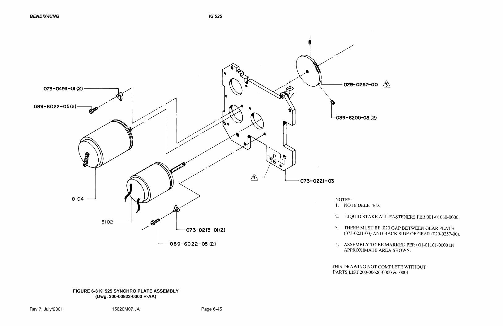
BENDIX/KING KI 525
Rev 7, July/2001 15620M07.JA Page 6-45
FIGURE 6-8 KI 525 SYNCHRO PLATE ASSEMBLY(Dwg. 300-00823-0000 R-AA)
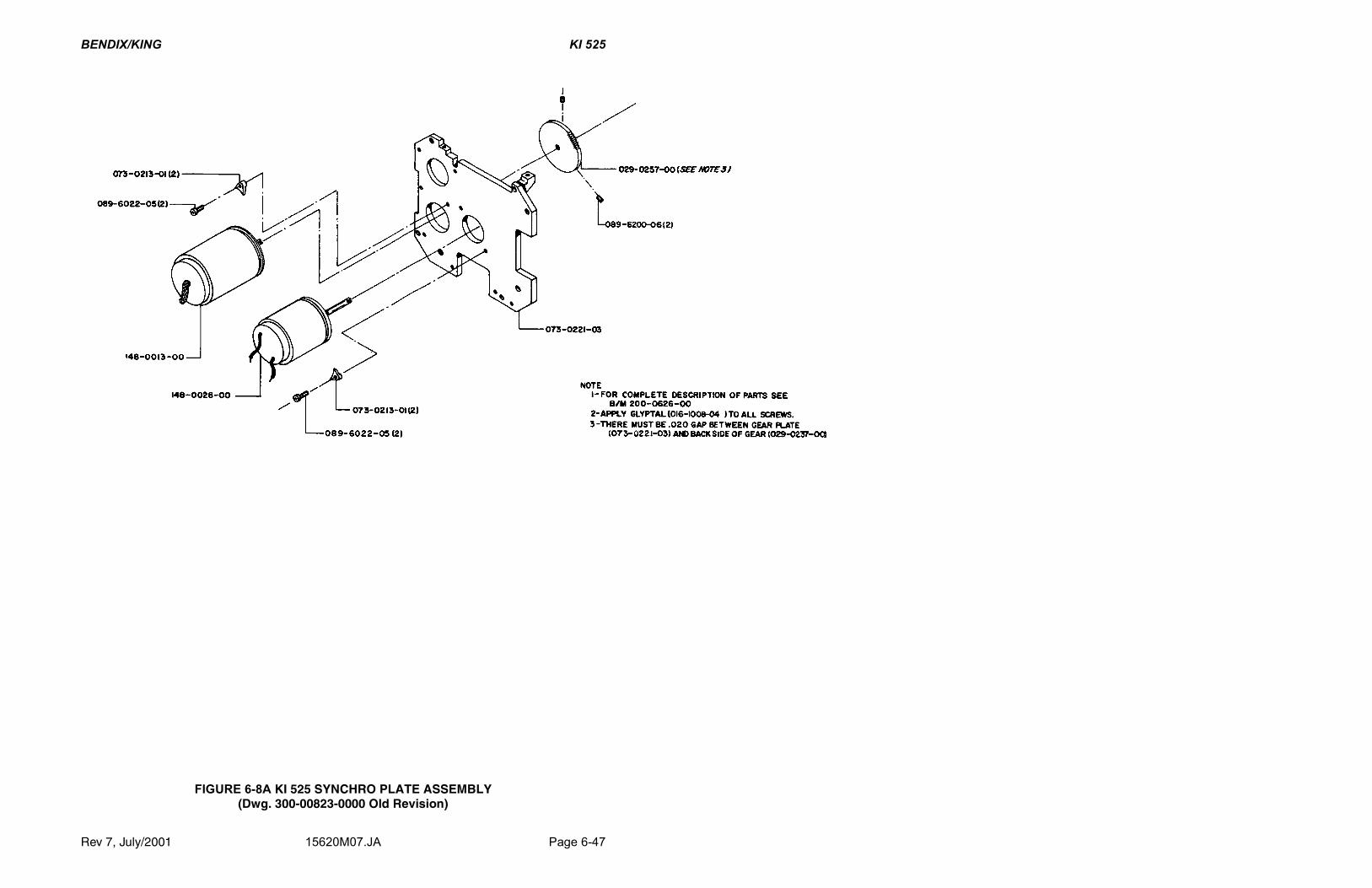
BENDIX/KING KI 525
Rev 7, July/2001 15620M07.JA Page 6-47
FIGURE 6-8A KI 525 SYNCHRO PLATE ASSEMBLY(Dwg. 300-00823-0000 Old Revision)

BENDIX/KING KI 525
Rev 7, July/2001 15620M07.JA Page 6-49
6.12 KI 525 YOKE ASSEMBLY
200-00625-0000 Rev. AA
---------------------------------------------------------------SYMBOL PART NUMBER FIND NO DESCRIPTION UM 0000---------------------------------------------------------------REF100 300-00822-0000 YOKE ASSEMBLY KI52 RF .00 023-00083-0000 MTR TO/FR FLAG EA 1.00 023-00084-0000 IND DEVIATION EA 1.00 047-02849-0001 CONTACT RING W/FIN EA 4.00 088-00346-0000 YOKE EA 1.00 088-00347-0002 MASK EA 1.00 088-00387-0000 GUARD EA 2.00 089-05899-0003 SCR PHP 2-56X3/16 EA 4.00 089-07046-0004 SCR PHS 2-56X1/4 EA 4.00

BENDIX/KING KI 525
Page 6-50 15620M07.JA Rev 7, July/2001
THIS PAGE IS RESERVED

BENDIX/KING KI 525
Rev 7, July/2001 15620M07.JA Page 6-51
FIGURE 6-9 KI 525 YOKE ASSEMBLY(Dwg. 300-00822-0000 R-AB)

BENDIX/KING KI 525
Rev 7, July/2001 15620M07.JA Page 6-53
FIGURE 6-9A KI 525 YOKE ASSEMBLY(Dwg. 300-00822-0000 Old Revision)

BENDIX/KING KI 525
Rev 7, July/2001 1562M07.JA Page 6-55
6.13 KI 525 DIFFERENTIAL CARRIER ASSEMBLY
200-00624-0000 Rev. 1
---------------------------------------------------------------SYMBOL PART NUMBER FIND NO DESCRIPTION UM 0000---------------------------------------------------------------REF100 300-00821-0000 DIFF CARRIER ASSY RF .00 029-00256-0000 GEAR SPUR 16T/64DP EA 2.00 029-00262-0001 GEAR SPUR 160T/64P EA 1.00 047-02850-0000 SHIM WASHER EA 4.00 076-00693-0000 PIN SPIDER GEAR EA 2.00

BENDIX/KING KI 525
Page 6-56 15620M07.JA Rev 7, July/2001
THIS PAGE IS RESERVED

BENDIX/KING KI 525
Rev 7, July/2001 15620M07.JA Page 6-57
FIGURE 6-10 KI 525 DIFFERENTIAL CARRIER ASSEMBLY(Dwg. 300-00821-0000 R-1)

BENDIX/KING KI 525
Rev 7, July/2001 15620M07.JA Page 6-59
FIGURE 6-10A KI 525 DIFFERENTIAL CARRIER ASSEMBLY(Dwg. 300-00821-0000 Old Revision)

BENDIX/KING KI 525
Rev 7, July/2001 15620M07.JA Page 6-61
6.14 KI 525 FLAG MECHANISM ASSEMBLY
200-00622-0000 Rev. AA200-00622-0001 Rev. AA
----------------------------------------------------------------------SYMBOL PART NUMBER FIND NO DESCRIPTION UM 0000 0001----------------------------------------------------------------------REF100 300-00819-0000 FLAG MECHANISM AS RF .00 . 016-01082-0000 DC RTV 3145 AR 1.00 1.00 016-01114-0000 EPXY TRA-CAST 3103 AR .00 .00 019-02185-0001 COIL FLG MCH 1430T EA 1.00 1.00 047-02847-0006 POLE .430 W/F EA 1.00 1.00 047-02847-0007 POLE .523 W/F EA 1.00 1.00 047-02848-0001 SPACER POLE W/F EA 2.00 2.00 088-00344-0000 HSG FLAG EA 1.00 1.00 088-00345-0001 COVER FLAG EA 1.00 1.00 090-00186-0000 RETAINER RING EA 1.00 1.00 200-00642-0001 FLAG ASSY EA . 1.00 200-00642-0003 FLAG ASSY EA 1.00 . 300-00819-0001 FLAG MECHANISM ASS RF . .00

BENDIX/KING KI 525
Page 6-62 15620M07.JA Rev 7, July/2001
THIS PAGE IS RESERVED

BENDIX/KING KI 525
Rev 7, July/2001 15620M07.JA Page 6-63
FIGURE 6-11 KI 525 FLAG MECHANISM ASSEMBLY(Dwg. 300-00819-0000 R-AB)

BENDIX/KING KI 525
Rev 7, July/2001 15620M07.JA Page 6-65
FIGURE 6-11A KI 525 FLAG MECHANISM ASSEMBLY(Dwg. 300-00819-0000 Old Revision)

BENDIX/KING KI 525
Rev 7, July/2001 15620M07.JA Page 6-67
FIGURE 6-12 KI 525 FLAG MECHANISM ASSEMBLY(Dwg. 300-00819-0001 R-AB)

BENDIX/KING KI 525
Rev 7, July/2001 15620M07.JA Page 6-69
FIGURE 6-12A KI 525 FLAG MECHANISM ASSEMBLY(Dwg. 300-00819-0001 Old Revision)

BENDIX/KING KI 525
Rev 7, July/2001 15620M07.JA Page 6-71
6.15 KI 525 FLAG ASSEMBLY
200-00642-0001 Rev. AB200-00642-0003 Rev. AA
----------------------------------------------------------------------SYMBOL PART NUMBER FIND NO DESCRIPTION UM 0001 0003----------------------------------------------------------------------REF100 300-05545-0000 NAV FLAG ASSY RF . .00 013-00017-0000 MAGNET EA 1.00 1.00 016-01122-0000 EPOXY DEVCON 14250 AR 1.00 1.00 047-02841-0002 FLAG PWR EA 1.00 . 047-10437-0003 FLAG EA . 1.00 300-00838-0001 FLAG ASSY RF .00 .
200-00642-0000 Rev. AA200-00642-0002 Rev. AA
----------------------------------------------------------------------SYMBOL PART NUMBER FIND NO DESCRIPTION UM 0000 0002---------------------------------------------------------------------- 013-00017-0000 MAGNET EA 1.00 1.00 016-01122-0000 EPOXY DEVCON 14250 AR 1.00 1.00 047-02841-0001 FLAG EA 1.00 . 047-02841-0003 FLAG EA . 1.00

BENDIX/KING KI 525
Page 6-72 15620M07.JA Rev 7, July/2001
THIS PAGE IS RESERVED

BENDIX/KING KI 525
Rev 7, July/2001 15620M07.JA Page 6-73
FIGURE 6-13 FLAG ASSEMBLY(Dwg. 300-05545-0000 Rev. AA)

BENDIX/KING KI 525
Page 6-74 15620M07.JA Rev 7, July/2001
THIS PAGE IS RESERVED

BENDIX/KING KI 525
Rev 7, July/2001 15620M07.JA Page 6-75
FIGURE 6-14 FLAG ASSEMBLY(Dwg. 300-00838-0000 Rev. 5)

BENDIX/KING KI 525
Page 6-76 15620M07.JA Rev 7, July/2001
THIS PAGE IS RESERVED

BENDIX/KING KI 525
Rev 7, July/2001 15620M07.JA Page 6-77
FIGURE 6-14A FLAG ASSEMBLY(Dwg. 300-00838-0000 Old Revision)

BENDIX/KING KI 525
Page 6-78 15620M07.JA Rev 7, July/2001
THIS PAGE IS RESERVED

BENDIX/KING KI 525
Rev 7, July/2001 15620M07.JA Page 6-79
FIGURE 6-15 FLAG ASSEMBLY(Dwg. 300-00838-0001 Rev. AA)

BENDIX/KING KI 525
Page 6-80 15620M07.JA Rev 7, July/2001
THIS PAGE IS RESERVED

BENDIX/KING KI 525
Rev 7, July/2001 15620M07.JA Page 6-81
FIGURE 6-15A FLAG ASSEMBLY(Dwg. 300-00838-0001 Old Revision)

BENDIX/KING KI 525
Page 6-82 15620M07.JA Rev 7, July/2001
THIS PAGE IS RESERVED

BENDIX/KING KI 525
Rev 7, July/2001 15620M07.JA Page 6-83
6.16 KI 525 REAR PLATE ASSEMBLY
200-00631-0000 Rev. AB
---------------------------------------------------------------SYMBOL PART NUMBER FIND NO DESCRIPTION UM 0000---------------------------------------------------------------B103 148-05035-0000 MOTOR STEPPER EA 1.00J102 030-02179-0000 CONN 41 PIN FEM EA 1.00REF100 300-00828-0000 ASSEMBLY, REAR GEA RF .00 016-01007-0005 LOCTITE 222 AR 1.00 016-01268-0000 LOCTITE 271 AR 1.00 029-00352-0000 GEAR 12/35T EA 2.00 029-00404-0000 GEAR 14T EA 1.00 030-01007-0000 TAB LOCKING EA 2.00 047-04782-0002 PLATE W/F & PVT EA 1.00 073-00222-0003 GEAR PLATE REAR EA 1.00 076-00820-0001 SPACER - COVER EA 1.00 089-05903-0003 SCR PHP 4-40X3/16 EA 2.00 089-06022-0004 SCR SHC 2-56X1/4 EA 2.00 090-00186-0000 RETAINER RING EA 2.00 150-00018-0010 TUBING SHRINK WHT IN 1.20

BENDIX/KING KI 525
Page 6-84 15620M07.JA Rev 7, July/2001
THIS PAGE IS RESERVED

BENDIX/KING KI 525
Rev 7, July/2001 15620M07.JA Page 6-85
FIGURE 6-16 KI 525 REAR PLATE ASSEMBLY(Dwg. 300-00828-0000 R-AB

BENDIX/KING KI 525
Rev 7, July/2001 15620M07.JA Page 6-87
FIGURE 6-16A KI 525 REAR PLATE ASSEMBLY(Dwg. 300-00828-0000 Old Revision)

BENDIX/KING KI 525
Rev 7, July/2001 15620M07.JA Page 6-89
6.17 KI 525 P.C. BOARD ASSEMBLY
200-00629-0000 Rev. 18
---------------------------------------------------------------SYMBOL PART NUMBER FIND NO DESCRIPTION UM 0000---------------------------------------------------------------C101 111-00001-0026 CAP CR .33UF 50V EA 1.00C104 111-00001-0030 CAP CR .68UF 50V EA 1.00C105 111-00001-0028 CAP CR .47UF 50V EA 1.00C108 096-01030-0005 CAP TN 10UF 10%20V EA 1.00C109 096-01030-0005 CAP TN 10UF 10%20V EA 1.00C110 096-01074-0002 CAPACITOR EA 1.00C115 111-00001-0000 CAP CR .01UF 50V EA 1.00C116 111-00001-0030 CAP CR .68UF 50V EA 1.00C117 111-00001-0030 CAP CR .68UF 50V EA 1.00C119 111-00001-0006 CAP CR .47UF 50V EA 1.00C120 111-02821-0051 CAP MC 820PF100V10 EA 1.00C121 113-03121-0000 CAP DC 120PF 500V EA 1.00C122 113-03121-0000 CAP DC 120PF 500V EA 1.00C123 113-03121-0000 CAP DC 120PF 500V EA 1.00C124 111-00001-0012 CAP CR .047UF 50V EA 1.00C125 111-00001-0012 CAP CR .047UF 50V EA 1.00CJ101 026-00018-0001 WIRE CKTJMPR 24AWG EA 1.00CJ102 026-00018-0001 WIRE CKTJMPR 24AWG EA 1.00CJ105 026-00018-0001 WIRE CKTJMPR 24AWG EA 1.00CJ106 026-00018-0001 WIRE CKTJMPR 24AWG EA 1.00CR101 007-06023-0000 DIO G 1N277 EA 1.00CR102 007-06023-0000 DIO G 1N277 EA 1.00CR103 007-06029-0000 DIO S 1N457A EA 1.00CR104 007-05045-0009 DIO Z 1/4M5.1AZ5 EA 1.00CR105 007-05044-0012 DIO Z 1N5530B 10V EA 1.00CR106 007-06029-0000 DIO S 1N457A EA 1.00CR107 007-06085-0000 DIO HC 1N5711 EA 1.00CR108 007-05045-0009 DIO Z 1/4M5.1AZ5 EA 1.00CR109 007-06029-0000 DIO S 1N457A EA 1.00CR110 007-05044-0012 DIO Z 1N5530B 10V EA 1.00CR111 007-07004-0001 SOLID STATE LAMP EA 1.00CR114 007-05051-0007 DIO Z 1N825A EA 1.00CR115 007-07004-0000 DIO L 5082-4480 EA 1.00CR116 007-06029-0000 DIO S 1N457A EA 1.00CR119 007-05011-0017 DIO Z 11V 1W 5% EA 1.00CR120 007-06029-0000 DIO S 1N457A EA 1.00CR121 007-06029-0000 DIO S 1N457A EA 1.00CR122 007-06029-0000 DIO S 1N457A EA 1.00CR123 007-06029-0000 DIO S 1N457A EA 1.00CR124 007-06029-0000 DIO S 1N457A EA 1.00CR125 007-06029-0000 DIO S 1N457A EA 1.00CR126 007-06029-0000 DIO S 1N457A EA 1.00CR127 007-05044-0009 DIO Z 1N5527B EA 1.00CR128 007-05044-0009 DIO Z 1N5527B EA 1.00CR129 007-06029-0000 DIO S 1N457A EA 1.00CR130 007-06029-0000 DIO S 1N457A EA 1.00DS101 037-00028-0006 LMP 5640 T1-1/4 14 EA 1.00DS102 037-00028-0006 LMP 5640 T1-1/4 14 EA 1.00

BENDIX/KING KI 525
Page 6-90 15620M07.JA Rev 7, July/2001
---------------------------------------------------------------SYMBOL PART NUMBER FIND NO DESCRIPTION UM 0000---------------------------------------------------------------I101 120-03053-0010 IC LM2904 SO PKG EA 1.00I102 120-03053-0010 IC LM2904 SO PKG EA 1.00I103 120-03052-0007 IC LM224D EA 1.00I105 120-03052-0007 IC LM224D EA 1.00J101 030-02152-0000 CONN 24P MALE EA 1.00Q104 007-00026-0003 XSTR S NPN 2N3416 EA 1.00Q109 007-00038-0000 XSTR S NPN 2N3053 EA 1.00R104 131-00391-0023 RES CF 390 QW 5% EA 1.00R105 131-00391-0023 RES CF 390 QW 5% EA 1.00R106 131-00273-0013 RES CF 27K EW 5% EA 1.00R107 131-00393-0013 RES CF 39K EW 5% EA 1.00R108 131-00222-0013 RES CF 2.2K EW 5% EA 1.00R109 132-00107-0059 RES WW 130 3.25W5% EA 1.00R110 131-00102-0033 RES CF 1K HW 5% EA 1.00R111 136-01003-0062 RES PF 100K EW 1% EA 1.00R112 136-01052-0062 RES PF 10.5K EW 1% EA .10R112 136-01072-0062 RES PF 10.7K EW 1% EA .10R112 136-01102-0062 RES PF 11K EW 1% EA .10R112 136-01132-0062 RES PF 11.3K EW 1% EA .10R112 136-01152-0062 RES PF 11.5K EW 1% EA .10R112 136-01182-0062 RES PF 11.8K EW 1% EA .10R112 136-01212-0062 RES PF 12.1K EW 1% EA .10R113 136-02211-0062 RES PF 2.21K EW 1% EA 1.00R114 131-00242-0033 RES CF 2.4K HW 5% EA 1.00R115 131-00102-0013 RES CF 1K EW 5% EA 1.00R116 131-00364-0013 RES CF 360K EW 5% EA 1.00R117 136-01003-0062 RES PF 100K EW 1% EA 1.00R118 136-01003-0062 RES PF 100K EW 1% EA 1.00R119 131-00181-0023 RES CF 180 QW 5% EA 1.00R120 131-00181-0023 RES CF 180 QW 5% EA 1.00R121 136-02492-0062 RES PF 24.9K EW 1% EA 1.00R122 136-02492-0062 RES PF 24.9K EW 1% EA 1.00R123 136-01001-0062 RES PF 1K EW 1% EA 1.00R124 136-02003-0062 RES PF 200K EW 1% EA 1.00R125 136-05111-0062 RES PF 5.11K EW 1% EA 1.00R126 136-01101-0062 RES PF 1.10K EW 1% EA 1.00R127 136-05111-0062 RES PF 5.11K EW 1% EA 1.00R128 136-02003-0062 RES PF 200K EW 1% EA 1.00R129 136-05112-0062 RES PF 51.1K EW 1% EA 1.00R130 136-04752-0062 RES PF 47.5K EW 1% EA 1.00R131 131-00204-0013 RES CF 200K EW 5% EA 1.00R133 131-00181-0023 RES CF 180 QW 5% EA 1.00R134 131-00333-0013 RES CF 33K EW 5% EA 1.00R135 136-02001-0062 RES PF 2K EW 1% EA 1.00R136 136-02001-0062 RES PF 2K EW 1% EA 1.00R137 136-03013-0062 RES PF 301K EW 1% EA 1.00R138 136-05111-0062 RES PF 5.11K EW 1% EA 1.00R139 136-01101-0062 RES PF 1.10K EW 1% EA 1.00R140 136-05111-0062 RES PF 5.11K EW 1% EA 1.00R141 136-03013-0062 RES PF 301K EW 1% EA 1.00R142 131-00623-0013 RES CF 62K EW 5% EA 1.00R143 131-00113-0013 RES CF 11K EW 5% EA 1.00

BENDIX/KING KI 525
Rev 7, July/2001 15620M07.JA Page 6-91
---------------------------------------------------------------SYMBOL PART NUMBER FIND NO DESCRIPTION UM 0000---------------------------------------------------------------R144 131-00153-0013 RES CF 15K EW 5% EA 1.00R145 136-02553-0062 RES PF 255K EW 1% EA 1.00R146 136-01333-0062 RES PF 133K EW 1% EA 1.00R146 136-01373-0072 RES PF 137K QW 1% EA 1.00R147 133-00100-0074 RES VA 200K QW 10% EA 1.00R148 136-02553-0062 RES PF 255K EW 1% EA 1.00R149 131-00911-0013 RES CF 910 EW 5% EA 1.00R150 131-00114-0013 RES CF 110K EW 5% EA 1.00R151 131-00513-0013 RES CF 51K EW 5% EA 1.00R153 131-00222-0023 RES CF 2.2K QW 5% EA 1.00R154 132-00105-0053 RES WW 91 1.5W 5% EA 1.00R160 131-00364-0013 RES CF 360K EW 5% EA 1.00R161 131-00132-0013 RES CF 1.3K EW 5% EA 1.00R162 131-00753-0013 RES CF 75K EW 5% EA 1.00R164 131-00513-0013 RES CF 51K EW 5% EA 1.00R165 131-00104-0013 RES CF 100K EW 5% EA 1.00R166 131-00683-0013 RES CF 68K EW 5% EA 1.00R167 136-07502-0062 RES PF 75.0K EW 1% EA 1.00R168 131-00513-0013 RES CF 51K EW 5% EA 1.00R169 133-00100-0075 RES VA 250K QW 10% EA 1.00R170 133-00100-0076 RES VA 500K QW 10% EA 1.00R171 132-00105-0053 RES WW 91 1.5W 5% EA 1.00R172 132-00106-0076 RES WW 500 2.25W5% EA 1.00R173 133-00100-0072 RES VA 50K QW 10% EA 1.00R174 131-00184-0013 RES CF 180K EW 5% EA 1.00R175 136-06042-0062 RES PF 60.4K EW 1% EA 1.00R176 136-02743-0062 RES PF 274K EW 1% EA 1.00R177 136-01003-0062 RES PF 100K EW 1% EA .01R177 136-01023-0062 RES PF 102K EW 1% EA .01R177 136-01053-0062 RES PF 105K EW 1% EA .01R177 136-01073-0062 RES PF 107K EW 1% EA .01R177 136-01103-0062 RES PF 110K EW 1% EA .01R177 136-01133-0062 RES PF 113K EW 1% EA .01R177 136-01153-0062 RES PF 115K EW 1% EA .01R177 136-01183-0062 RES PF 118K EW 1% EA .01R177 136-01213-0062 RES PF 121K EW 1% EA .01R177 136-01243-0062 RES PF 124K EW 1% EA .01R177 136-01273-0062 RES PF 127K EW 1% EA .01R177 136-01303-0062 RES PF 130K EW 1% EA .01R177 136-01333-0062 RES PF 133K EW 1% EA .01R177 136-01373-0062 RES PF 137K EW 1% EA .01R177 136-01403-0062 RES PF 140K EW 1% EA .90R177 136-01433-0062 RES PF 143K EW 1% EA .01R177 136-01473-0062 RES PF 147K EW 1% EA .01R177 136-01503-0062 RES PF 150K EW 1% EA .01R177 136-01583-0062 RES PF 158K1/8W1% EA .01R177 136-01623-0062 RES PF 162K EW 1% EA .01R177 136-01653-0062 RES PF 165K EW 1% EA .01R177 136-01693-0062 RES PF 169K EW 1% EA .01R177 136-01743-0062 RES PF 174K EW 1% EA .01R177 136-01783-0062 RES PF 178K EW 1% EA .01R177 136-01823-0062 RES PF 182K EW 1% EA .01

BENDIX/KING KI 525
Page 6-92 15620M07.JA Rev 7, July/2001
---------------------------------------------------------------SYMBOL PART NUMBER FIND NO DESCRIPTION UM 0000---------------------------------------------------------------R177 136-01873-0062 RES PF 187K EW 1% EA .01R177 136-01913-0062 RES PF 191K EW 1% EA .01R177 136-01963-0062 RES PF 196K EW 1% EA .01R177 136-02003-0062 RES PF 200K EW 1% EA .01R177 136-02053-0062 RES PF 205K EW 1% EA .01R177 136-02103-0062 RES PF 210K EW 1% EA .01R178 136-04873-0062 RES PF 487K EW 1% EA 1.00R179 136-07502-0062 RES PF 75.0K EW 1% EA 1.00R180 136-01433-0062 RES PF 143K EW 1% EA 1.00R181 136-04873-0062 RES PF 487K EW 1% EA 1.00R182 136-01003-0062 RES PF 100K EW 1% EA .01R182 136-01023-0062 RES PF 102K EW 1% EA .01R182 136-01053-0062 RES PF 105K EW 1% EA .01R182 136-01073-0062 RES PF 107K EW 1% EA .01R182 136-01103-0062 RES PF 110K EW 1% EA .01R182 136-01133-0062 RES PF 113K EW 1% EA .01R182 136-01153-0062 RES PF 115K EW 1% EA .01R182 136-01183-0062 RES PF 118K EW 1% EA .01R182 136-01213-0062 RES PF 121K EW 1% EA .01R182 136-01243-0062 RES PF 124K EW 1% EA .01R182 136-01273-0062 RES PF 127K EW 1% EA .01R182 136-01303-0062 RES PF 130K EW 1% EA .01R182 136-01333-0062 RES PF 133K EW 1% EA .01R182 136-01373-0062 RES PF 137K EW 1% EA .01R182 136-01403-0062 RES PF 140K EW 1% EA .90R182 136-01433-0062 RES PF 143K EW 1% EA .01R182 136-01473-0062 RES PF 147K EW 1% EA .01R182 136-01503-0062 RES PF 150K EW 1% EA .01R182 136-01583-0062 RES PF 158K1/8W1% EA .01R182 136-01623-0062 RES PF 162K EW 1% EA .01R182 136-01653-0062 RES PF 165K EW 1% EA .01R182 136-01693-0062 RES PF 169K EW 1% EA .01R182 136-01743-0062 RES PF 174K EW 1% EA .01R182 136-01783-0062 RES PF 178K EW 1% EA .01R182 136-01823-0062 RES PF 182K EW 1% EA .01R182 136-01873-0062 RES PF 187K EW 1% EA .01R182 136-01913-0062 RES PF 191K EW 1% EA .01R182 136-01963-0062 RES PF 196K EW 1% EA .01R182 136-02003-0062 RES PF 200K EW 1% EA .01R182 136-02053-0062 RES PF 205K EW 1% EA .01R182 136-02103-0062 RES PF 210K EW 1% EA .01R183 136-02743-0062 RES PF 274K EW 1% EA 1.00R184 131-00513-0013 RES CF 51K EW 5% EA 1.00R185 134-01055-0000 PTC THERMISTOR EA 1.00R186 134-01055-0000 PTC THERMISTOR EA 1.00R187 131-00153-0013 RES CF 15K EW 5% EA 1.00R188 131-00394-0013 RES CF 390K EW 5% EA 1.00R189 136-05112-0062 RES PF 51.1K EW 1% EA 1.00R190 136-01433-0062 RES PF 143K EW 1% EA 1.00R191 136-05112-0062 RES PF 51.1K EW 1% EA 1.00R192 131-00394-0013 RES CF 390K EW 5% EA 1.00R193 136-06042-0062 RES PF 60.4K EW 1% EA 1.00

BENDIX/KING KI 525
Rev 7, July/2001 15620M07.JA Page 6-93
---------------------------------------------------------------SYMBOL PART NUMBER FIND NO DESCRIPTION UM 0000---------------------------------------------------------------R194 133-00100-0076 RES VA 500K QW 10% EA 1.00R195 133-00100-0076 RES VA 500K QW 10% EA 1.00R196 133-00100-0076 RES VA 500K QW 10% EA 1.00R197 133-00100-0076 RES VA 500K QW 10% EA 1.00R198 131-00301-0023 RES CF 300 QW 5% EA 1.00R199 131-00301-0023 RES CF 300 QW 5% EA 1.00V101 134-05006-0002 PHOTOCELL EA 1.00V102 134-05006-0002 PHOTOCELL EA 1.00 009-05660-0060 PC BOARD EA 1.00 016-01008-0004 GLYPTAL 7526 BL AR 1.00 016-01040-0000 COATING TYPE AR AR .00 016-01122-0000 EPOXY DEVCON 14250 AR .00 047-02800-0002 SHUTTER W/F EA 2.00 047-02844-0001 SLIP RING BRSH W/F EA 4.00 088-00336-0008 FLTR LAMP WHT/BLU EA 2.00 088-00337-0001 HSG PICK OFF EA 2.00 089-02326-0000 NUT TWIN 2-56 EA 2.00 089-05899-0004 SCR PHP 2-56X1/4 EA 8.00 089-08012-0037 WSHR INTL LK #2 EA 8.00 091-00210-0000 INSUL XSTR EA 1.00 092-05015-0006 EYE FUNN .030X.088 EA 4.00 150-00003-0010 TUBING TFLN 24AWG IN 1.20 150-00005-0010 TUBING TFLN 20AWG IN 2.00 300-00826-0000 PCB ASSY RF .00

BENDIX/KING KI 525
Page 6-94 15620M07.JA Rev 7, July/2001
THIS PAGE IS RESERVED

BENDIX/KING KI 525
Rev 7, July/2001 15620M07.JA Page 6-95
FIGURE 6-17 KI 525 P.C. BOARD ASSEMBLY(Dwg. 300-00826-0000 R-12)

BENDIX/KING KI 525
Rev 7, July/2001 15620M07.JA Page 6-97
FIGURE 6-17A KI 525 P.C. BOARD ASSEMBLY(Dwg. 300-00826-0000 R-4)

BENDIX/KING KI 525
Rev 7, July/2001 15620M07.JA Page 6-99
FIGURE 6-18 KI 525 P.C. BOARD SCHEMATIC(Dwg. 002-00306-0000 R-9)

BENDIX/KING KI 525
Rev 7, July/2001 15620M07.JA Page 6-101
FIGURE 6-18A KI 525 P.C. BOARD SCHEMATIC(Dwg. 002-00306-0000 R-6)

BENDIX/KING KI 525
Rev 7, July/2001 15620M07.JA Page 6-103
6.18 KI 525 GLIDESLOPE PLATE ASSEMBLY
200-00643-0000 Rev. AA
---------------------------------------------------------------SYMBOL PART NUMBER FIND NO DESCRIPTION UM 0000---------------------------------------------------------------CR117 007-07004-0000 DIO L 5082-4480 EA 1.00REF100 300-00839-0000 GLIDESLOPE PLATE RF .00 013-00018-0000 MAGNET EA 1.00 016-01013-0000 VAC GREASE DC 976 AR .00 016-01122-0000 EPOXY DEVCON 14250 AR 1.00 019-02184-0000 COIL 125T EA 1.00 047-04621-0003 POLE MGNT EA 1.00 047-04621-0005 POLE MGNT EA 1.00 073-00217-0002 PLATE GS EA 1.00 073-00941-0001 GS SUPPORT W/FIN EA 1.00 076-00694-0001 SHAFT MAGNET W/F EA 1.00 089-05107-0004 SCR, MACH, 2-56, F EA 4.00 089-08054-0030 WSHR FLT STD .128 AR .00 089-08170-0030 WSHR FLT STD .128 AR .00 090-00019-0000 RING RTNR .125 EA 1.00 147-05006-0008 BEARING BALL EA 2.00 150-00018-0010 TUBING SHRINK WHT IN 12.00

BENDIX/KING KI 525
Page 6-104 15620M07.JA Rev 7, July/2001
THIS PAGE IS RESERVED

BENDIX/KING KI 525
Rev 7, July/2001 15620M07.JA Page 6-105
FIGURE 6-19 KI 525 GLIDE SLOPE PLATE ASSEMBLY(Dwg. 300-00839-0000 R-16)

BENDIX/KING KI 525
Rev 7, July/2001 15620M07.JA Page 6-107
FIGURE 6-19A KI 525 GLIDE SLOPE PLATE ASSEMBLY(Dwg. 300-00839-0000 Old Revision)