kishore padmaraju* and keren bergman resolving the …kishore/publications/np_2013.pdf · kishore...
TRANSCRIPT
DOI 10.1515/nanoph-2013-0013 Nanophotonics 2013; aop
Review
Kishore Padmaraju* and Keren Bergman
Resolving the thermal challenges for silicon microring resonator devices Abstract: Silicon microring resonators have been hailed for their potential use in next-generation optical inter-connects. However, the functionality of silicon microring based devices suffer from susceptibility to thermal fluc-tuations that is often overlooked in their demonstrated results, but must be resolved for their future implemen-tation in microelectronic applications. We survey the emerging efforts that have been put forth to resolve these thermal susceptibilities and provide a comprehensive discussion of their advantages and disadvantages.
Keywords: integrated photonics; microring resonators; optical interconnects; silicon photonics
*Corresponding author: Kishore Padmaraju, Department of Electrical Engineering, Columbia University, 500 West 120th Street, New York, NY, USA, e-mail: [email protected] Keren Bergman: Department of Electrical Engineering, Columbia University, 500 West 120th Street, New York, NY, USA
Edited by Michal Lipson
1 Silicon microring resonator based devices
The growing bandwidth needs within data applications have motivated the replacement of traditionally elec-tronic links with optical links for information networks as diverse as data centers, supercomputers, and fiber-optic access networks [1, 2]. Applications such as these stress the traditional portfolio of optical components, rebalanc-ing the emphasis from expensive high-performance com-ponents towards low-cost high-volume components that can be closely integrated with electronics. With these con-siderations in mind, the silicon photonics platform has received wide attention for its ability to deliver the nec-essary bandwidth required at an economy-of-scale that will be enabled by its compatibility with CMOS fabrication processes [3].
Within the silicon photonic platform, traditional optical components such as low-loss waveguides [4], low-loss waveguide crossings [5], high-speed mach-zhender modulators (MZM) [6], arrayed waveguide-gratings [7], and efficient photodetectors [8, 9] have been demon-strated. Leveraging the high index contrast between silicon and silicon-on-insulator, the aforementioned com-ponents have been shown with much smaller footprints than their counterparts in more conventional optical plat-forms. For active devices, these smaller footprints directly translate to higher energy-efficiencies.
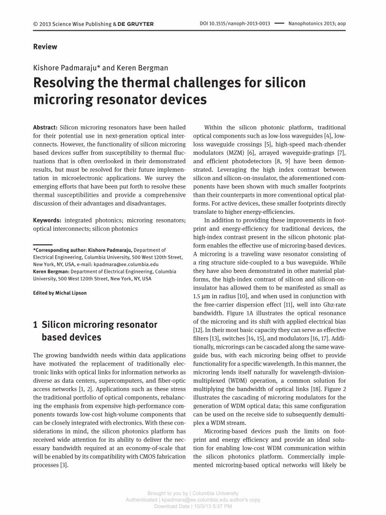
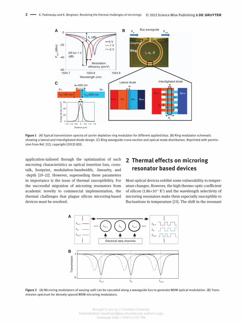
In addition to providing these improvements in foot-print and energy-efficiency for traditional devices, the high-index contrast present in the silicon photonic plat-form enables the effective use of microring-based devices. A microring is a traveling wave resonator consisting of a ring structure side-coupled to a bus waveguide. While they have also been demonstrated in other material plat-forms, the high-index contrast of silicon and silicon-on-insulator has allowed them to be manifested as small as 1.5 µ m in radius [10], and when used in conjunction with the free-carrier dispersion effect [11], well into Ghz-rate bandwidth. Figure 1 A illustrates the optical resonance of the microring and its shift with applied electrical bias [12]. In their most basic capacity they can serve as effective filters [13], switches [14, 15], and modulators [16, 17]. Addi-tionally, microrings can be cascaded along the same wave-guide bus, with each microring being offset to provide functionality for a specific wavelength. In this manner, the microring lends itself naturally for wavelength-division-multiplexed (WDM) operation, a common solution for multiplying the bandwidth of optical links [18]. Figure 2 illustrates the cascading of microring modulators for the generation of WDM optical data; this same configuration can be used on the receive side to subsequently demulti-plex a WDM stream.
Microring-based devices push the limits on foot-print and energy efficiency and provide an ideal solu-tion for enabling low-cost WDM communication within the silicon photonics platform. Commercially imple-mented microring-based optical networks will likely be
© 2013 Science Wise Publishing &
Brought to you by | Columbia UniversityAuthenticated | [email protected] author's copy
Download Date | 10/3/13 5:37 PM
2 K. Padmaraju and K. Bergman: Resolving the thermal challenges of microrings
application-tailored through the optimization of such microring characteristics as optical insertion loss, cross-talk, footprint, modulation-bandwidth, -linearity, and -depth [19 – 22]. However, superseding these parameters in importance is the issue of thermal susceptibility. For the successful migration of microring resonators from academic novelty to commercial implementation, the thermal challenges that plague silicon microring-based devices must be resolved.
2 Thermal effects on microring resonator based devices
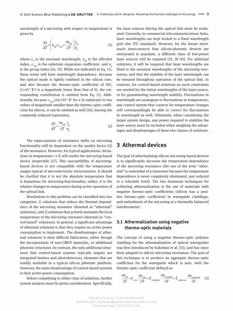
Most optical devices exhibit some vulnerability to temper-ature changes. However, the high thermo-optic coefficient of silicon (1.86 × 10 -4 K -1 ) and the wavelength selectivity of microring resonators make them especially susceptible to fluctuations in temperature [23]. The shift in the resonant
A
IL (dB)
Bus waveguidePin Pout0
-20
-40
-601554.7 1554.8 1554.9
Lateral diode Interdigitated diodew=450 nm
w
P+
60
40
20
0-1.5 -0.5 0.5 1.5
Distance (µm)
Ene
rgy
dens
ity (
nJ/m
3 )
1.00-1.0
N+
N+N+
dD
df
d1
P+P++
P++ P+
N++
N++hw=220 nmhs=150 nm
w w
Wavelength (nm)
ER for 1 V(dB)P
out (
dBm
)
0 V-1 V-2 V
Modulationefficiency (pm/V)
C
B
Figure 1 (A) Typical transmission spectra of carrier depletion ring modulator for different applied bias. (B) Ring modulator schematic showing a lateral and interdigitated diode design. (C) Ring waveguide cross-section and optical mode distribution. Reprinted with permis-sion from Ref. [12], copyright (2013) IEEE.
A
Electrical data channels
Tra
nsm
issi
on
0λn-1
λn-1
λn-1
λn
λnλn
λn+1
λn+1
λn+1
λn-1
λn
λn+1
1B
Figure 2 (A) Microring modulators of varying radii can be cascaded along a waveguide bus to generate WDM optical modulation. (B) Trans-mission spectrum for densely spaced WDM microring modulators.
© 2013 Science Wise Publishing &
Brought to you by | Columbia UniversityAuthenticated | [email protected] author's copy
Download Date | 10/3/13 5:37 PM
K. Padmaraju and K. Bergman: Resolving the thermal challenges of microrings 3
wavelength of a microring with respect to temperature is given by
0effeff sub
g
nd ndT T n
λλα
⎛ ⎞∂= +⎜ ⎟∂⎝ ⎠
(1)
where λ 0 is the resonant wavelength, n eff is the effective index, α sub is the substrate expansion coefficient, and n g is the group index [24, 25]. While not indicated in Eq. (1), these terms will have wavelength dependence. Because the optical mode is tightly confined in the silicon core, and also because the thermo-optic coefficient of SiO 2 (1 × 10 -5 K -1 ) is a magnitude lower than that of Si, the cor-responding contribution is omitted from Eq. (1). Addi-tionally, because α sub (2.6 × 10 -6 K -1 for a Si substrate) is two orders of magnitude smaller than the thermo-optic coeffi-cient for silicon, it can be omitted as well [26], leaving the commonly reduced expression,
0eff
g
nddT T n
λλ ∂=
∂
(2)
The repercussions of resonance shifts on microring functionality will be dependent on the quality factor (Q) of the resonance. However, for typical applications, devia-tions in temperature > 1 K will render the microring-based device inoperable [27]. This susceptibility of microring-based devices is not compatible with the temperature ranges typical of microelectronic environments. It should be clarified that it is not the absolute temperature that is hazardous for microring-functionality; rather, it is the relative changes in temperature during active operation of the optical link.
Resolutions to this problem can be classified into two categories: 1) solutions that reduce the thermal depend-ence of the microring resonator (denoted as “ athermal ” solutions), and 2) solutions that actively maintain the local temperature of the microring resonator (denoted as “ con-trol-based ” solutions). In general, a significant advantage of athermal solutions is that they require no active power consumption to implement. The disadvantages of ather-mal solutions is their difficult fabrication, either though the incorporation of non-CMOS materials, or additional photonic structures. In contrast, the only additional struc-tures that control-based systems typically require are integrated heaters and photodetectors, elements that are readily available in a typical silicon photonic platform. However, the main disadvantage of control-based systems is their active power consumption.
Before committing to either class of solutions, further system analysis must be given consideration. Specifically,
the laser sources driving the optical link must be evalu-ated. Currently, in commercial telecommunications links, laser wavelengths are kept locked to a fixed wavelength grid (the ITU standard). However, for the future short-reach interconnects that silicon-photonic devices are envisioned to populate, a different class of low-power laser sources will be required [19, 28 – 30]. For athermal solutions, it will be required that laser wavelengths are fixed to the resonant wavelengths of the microring reso-nators, and that the stability of the laser wavelength can be ensured throughout operation of the optical link. In contrast, for control-based solutions no such constraints are needed for the initial wavelengths of the laser source, or for guaranteeing wavelength stability. Fluctuations in wavelength are analogous to fluctuations in temperature; any control system that corrects for temperature changes will correspondingly be able to correct for fluctuations in wavelength as well. Ultimately, when considering the larger system design, any power required to stabilize the laser source must be included when weighing the advan-tages and disadvantages of these two classes of solutions.
3 Athermal devices The goal of athermalizing silicon microring-based devices is to significantly decrease the temperature-dependence of the microring resonance (the use of the term “ ather-mal ” is somewhat of a misnomer because the temperature dependence is never completely eliminated, just reduced to a tolerable level). The two dominant techniques for achieving athermalization is the use of materials with negative thermo-optic coefficients (silicon has a posi-tive thermo-optic coefficient) in waveguide claddings, and embedment of the microring in a thermally balanced interferometer.
3.1 Athermalization using negative thermo-optic materials
The concept of using a negative thermo-optic polymer cladding for the athermalization of optical waveguides was first introduced by Kokobun et al. [31], and has since been adapted to silicon microring resonators. The goal of this technique is to produce an aggregate thermo-optic coefficient for the waveguide which is zero, with the thermo-optic coefficient defined as
claddingeff core substrate
core cladding substrate
nn n nT T T T
Γ Γ Γ∂∂ ∂ ∂
= + +∂ ∂ ∂ ∂
(3)
© 2013 Science Wise Publishing &
Brought to you by | Columbia UniversityAuthenticated | [email protected] author's copy
Download Date | 10/3/13 5:37 PM
4 K. Padmaraju and K. Bergman: Resolving the thermal challenges of microrings
where Γ is the modal confinement factors for the core, cladding, and substrate, as specified [32]. The modal confinement and negative thermo-optic coefficient of the cladding are engineered to balance the modal con-finement and positive thermo-optic coefficients of the core (silicon) and substrate (silicon dioxide). It should be noted that the wavelength dependency is not denoted in Eq. (3), and furthermore, only linear terms have been included. Higher-order wavelength dependencies of the thermo-optic coefficient make it difficult to achieve ather-mal behavior over a broad wavelength and temperature range [32, 33].
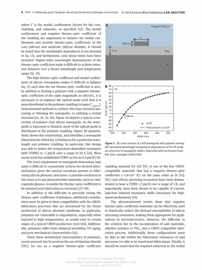
The high thermo-optic coefficient and modal confine-ment of silicon waveguides makes it difficult to balance Eq. (3) such that the net thermo-optic coefficient is zero. In addition to finding a polymer with a negative thermo-optic coefficient of the same magnitude as silicon ’ s, it is necessary to re-engineer the optical mode such that it is more distributed in the polymer cladding (a larger Γ cladding ). Demonstrated methods to achieve this have involved nar-rowing or thinning the waveguide, or utilizing a slotted structure [24, 26, 34 – 36]. Figure 3 A depicts a typical cross-section of polymer-clad silicon waveguide. As the wave-guide is narrowed or thinned, more of the optical mode is distributed in the polymer cladding. Figure 3B quantita-tively shows this relationship, and identifies a waveguide dimension for which Eq. (3) balances for a particular wave-length and polymer cladding. In particular, this design was able to reduce the temperature dependent resonance shift (TDWS) to -5 pm/K over a range of 50 K [24]. More recent work has established TDWS as low as 0.2 pm/K [33].
The strict requirement on waveguide dimensions may make it difficult to consistently achieve the desired ather-malization given the natural variations present in fabri-cating silicon photonic structures. A possible resolution to this issue is to use photosensitive materials, such as chal-cogenide glasses, to enable the thermo-optic coefficient to be trimmed post-fabrication as necessary [37 – 39].
In addition to the difficulty in precisely tuning the thermo-optic coefficient of polymers, additional consider-ation must be given to their compatibility with the CMOS-fabrication processes that are envisioned for the future production of silicon photonic platforms. In particular, polymers are vulnerable to degradation, especially when exposed to high temperatures, as would exist in certain stages of a typical CMOS-production cycle [40]. Addition-ally, polymers suffer from chemical instability, UV aging, and poor mechanical characteristics [41].
Given these detrimental characteristics of polymers, recent research has focused on the use of titanium dioxide (TiO 2 ) for use as a negative thermo-optic coefficient
A
220 nm
2 µm SiO2
Si
Polymer PSQ-LH
w
B 80
70
60
50
40
30dλ
/dT
(pm
/°C
)20
10
-10
-20
-30
-40
-50250 300 350 400
306 nm
TE
dλ/dT
Polynomial fit of dλ/dT
Width (nm)450 500
0
Figure 3 (A) cross-section of a SOI waveguide with polymer overlay. (B) Calculated wavelength temperature dependence of the TE mode as a function of waveguide widths. Reprinted with permission from Ref. [24], copyright (2009) OSA.
cladding material [41 – 44] TiO 2 is one of the few CMOS-compatible materials that has a negative thermo-optic coefficient (~-1.8 × 10 -4 K -1 ) on the same order as Si [42]. TiO 2 -clad silicon microring resonators have been demon-strated to have a TDWS < 2 pm/K over a range of 5 K, and importantly, have been shown to be capable of current-injection induced resonance shifts (necessary for high-speed modulation) [43].
The aforementioned results show that negative thermo-optic coefficient materials can be effectively used to drastically reduce the thermal susceptibility of silicon microring resonators, making them appropriate for appli-cations in microelectronics. However, the difficulty in the solution lies in the incorporation of said materials, whether polymer or TiO 2 , into a CMOS compatible fabri-cation process. Additionally, these configurations must be able to fall within the fabrication tolerances of said processes (or able to be tuned post-fabrication). Finally, it should be noted that the required reduction in the modal
© 2013 Science Wise Publishing &
Brought to you by | Columbia UniversityAuthenticated | [email protected] author's copy
Download Date | 10/3/13 5:37 PM
K. Padmaraju and K. Bergman: Resolving the thermal challenges of microrings 5
confinement of the core will have consequences on the losses of the microring in straight and bent configura-tions, negatively impacting such desired attributes as footprint and Q-factor [32].
3.2 Athermalization using an interferometric structure
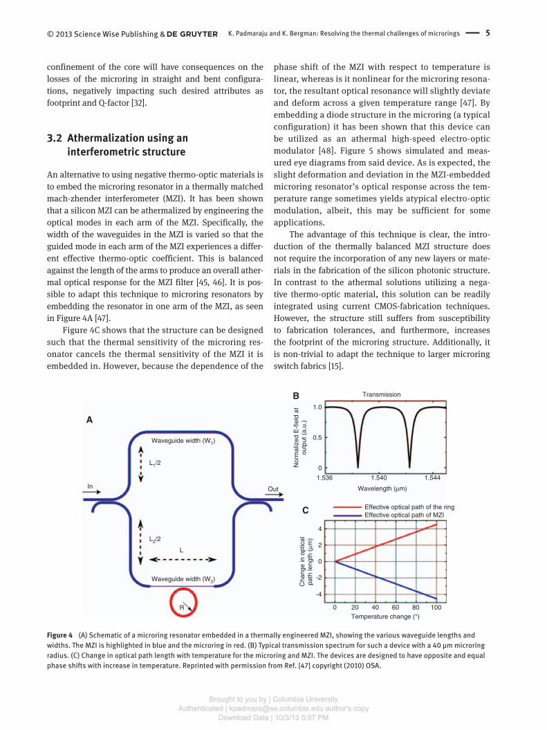
An alternative to using negative thermo-optic materials is to embed the microring resonator in a thermally matched mach-zhender interferometer (MZI). It has been shown that a silicon MZI can be athermalized by engineering the optical modes in each arm of the MZI. Specifically, the width of the waveguides in the MZI is varied so that the guided mode in each arm of the MZI experiences a differ-ent effective thermo-optic coefficient. This is balanced against the length of the arms to produce an overall ather-mal optical response for the MZI filter [45, 46]. It is pos-sible to adapt this technique to microring resonators by embedding the resonator in one arm of the MZI, as seen in Figure 4 A [47].
Figure 4 C shows that the structure can be designed such that the thermal sensitivity of the microring res-onator cancels the thermal sensitivity of the MZI it is embedded in. However, because the dependence of the
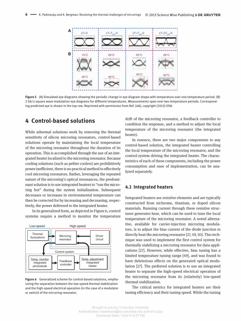
phase shift of the MZI with respect to temperature is linear, whereas is it nonlinear for the microring resona-tor, the resultant optical resonance will slightly deviate and deform across a given temperature range [47]. By embedding a diode structure in the microring (a typical configuration) it has been shown that this device can be utilized as an athermal high-speed electro-optic modulator [48]. Figure 5 shows simulated and meas-ured eye diagrams from said device. As is expected, the slight deformation and deviation in the MZI-embedded microring resonator ’ s optical response across the tem-perature range sometimes yields atypical electro-optic modulation, albeit, this may be sufficient for some applications.
The advantage of this technique is clear, the intro-duction of the thermally balanced MZI structure does not require the incorporation of any new layers or mate-rials in the fabrication of the silicon photonic structure. In contrast to the athermal solutions utilizing a nega-tive thermo-optic material, this solution can be readily integrated using current CMOS-fabrication techniques. However, the structure still suffers from susceptibility to fabrication tolerances, and furthermore, increases the footprint of the microring structure. Additionally, it is non-trivial to adapt the technique to larger microring switch fabrics [15].
A
Waveguide width (W1)
Waveguide width (W2)
In
1.0
0.5
0
4
2
0
-2
-4
1.536
0 20 40 60 80 100
1.540
Wavelength (µm)
Temperature change (°)
Transmission
Effective optical path of the ringEffective optical path of MZI
1.544
Out
L1/2
L2/2
L
R
B
C
Nor
mal
ized
E-f
ield
at
outp
ut (
a.u.
)C
hang
e in
opt
ical
path
leng
th (
µm)
Figure 4 (A) Schematic of a microring resonator embedded in a thermally engineered MZI, showing the various waveguide lengths and widths. The MZI is highlighted in blue and the microring in red. (B) Typical transmission spectrum for such a device with a 40 µ m microring radius. (C) Change in optical path length with temperature for the microring and MZI. The devices are designed to have opposite and equal phase shifts with increase in temperature. Reprinted with permission from Ref. [47] copyright (2010) OSA.
© 2013 Science Wise Publishing &
Brought to you by | Columbia UniversityAuthenticated | [email protected] author's copy
Download Date | 10/3/13 5:37 PM
6 K. Padmaraju and K. Bergman: Resolving the thermal challenges of microrings
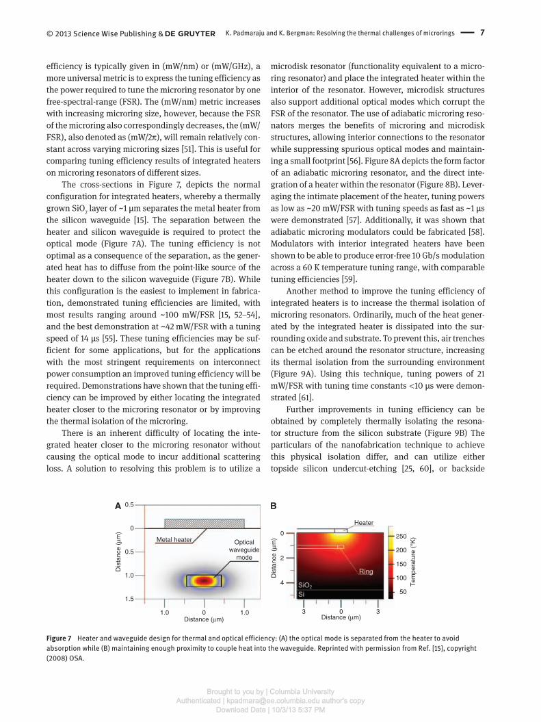
4 Control-based solutions While athermal solutions work by removing the thermal sensitivity of silicon microring resonators, control-based solutions operate by maintaining the local temperature of the microring resonator throughout the duration of its operation. This is accomplished through the use of an inte-grated heater localized to the microring resonator. Because cooling solutions (such as peltier coolers) are prohibitively power inefficient, there is no practical method to effectively cool microring resonators. Rather, leveraging the repeated nature of the microring ’ s optical resonances, the predomi-nant solution is to use integrated heaters to “ run the micro-ring hot ” during the system initialization. Subsequent decreases or increases in environmental temperature can then be corrected for by increasing and decreasing, respec-tively, the power delivered to the integrated heater.
In its generalized form, as depicted in Figure 6 , control systems require a method to monitor the temperature
A∆T=0
15°C 25°C20°C 30°C
35°C45°C
40°C50°C
∆T=Tper/4 ∆T=Tper/2 ∆T=3Tper/4
B
Figure 5 (A) Simulated eye diagrams showing the periodic change in eye diagram shape with temperature over one temperature period. (B) 2 Gb/s square wave modulation eye diagrams for different temperatures. Measurements span over two temperature periods. Correspond-ing predicted eye is shown in the top row. Reprinted with permission from Ref. [48], copyright (2012) OSA.
Temp. monitorIntegratedphotodiode
Temp. adjustmentIntegrated
heater
Microringresonator
Drivercircuit
Thermalfluctuations
Control system
Feedbackcontroller
Low-speed High-speed
Figure 6 Generalized scheme for control-based solutions, empha-sizing the separation between the low-speed thermal stabilization and the high-speed electrical operation (in the case of a modulator or switch) of the microring resonator.
drift of the microring resonator, a feedback controller to condition the response, and a method to adjust the local temperature of the microring resonator (the integrated heater).
In essence, there are two major components to any control-based solution, the integrated heater controlling the local temperature of the microring resonator, and the control-system driving the integrated heater. The charac-teristics of each of these components, including the power consumption and ease of implementation, can be ana-lyzed separately.
4.1 Integrated heaters
Integrated heaters are resistive elements and are typically constructed from nichrome, titanium, or doped silicon materials. Running current through these resistive struc-tures generates heat, which can be used to tune the local temperature of the microring resonator. A noted alterna-tive, available for carrier-injection microring modula-tors, is to adjust the bias current of the diode junction to directly heat the microring resonator [27, 49, 50]. This tech-nique was used to implement the first control system for thermally stabilizing a microring resonator for data appli-cations [27]. However, while effective, bias tuning has a limited temperature tuning range [49], and was found to have deleterious effects on the generated optical modu-lation [27]. The preferred solution is to use an integrated heater to separate the high-speed electrical operation of the microring resonator from its (relatively) low-speed thermal stabilization.
The critical metrics for integrated heaters are their tuning efficiency and their tuning speed. While the tuning
© 2013 Science Wise Publishing &
Brought to you by | Columbia UniversityAuthenticated | [email protected] author's copy
Download Date | 10/3/13 5:37 PM
K. Padmaraju and K. Bergman: Resolving the thermal challenges of microrings 7
efficiency is typically given in (mW/nm) or (mW/GHz), a more universal metric is to express the tuning efficiency as the power required to tune the microring resonator by one free-spectral-range (FSR). The (mW/nm) metric increases with increasing microring size, however, because the FSR of the microring also correspondingly decreases, the (mW/FSR), also denoted as (mW/2 π ), will remain relatively con-stant across varying microring sizes [51]. This is useful for comparing tuning efficiency results of integrated heaters on microring resonators of different sizes.
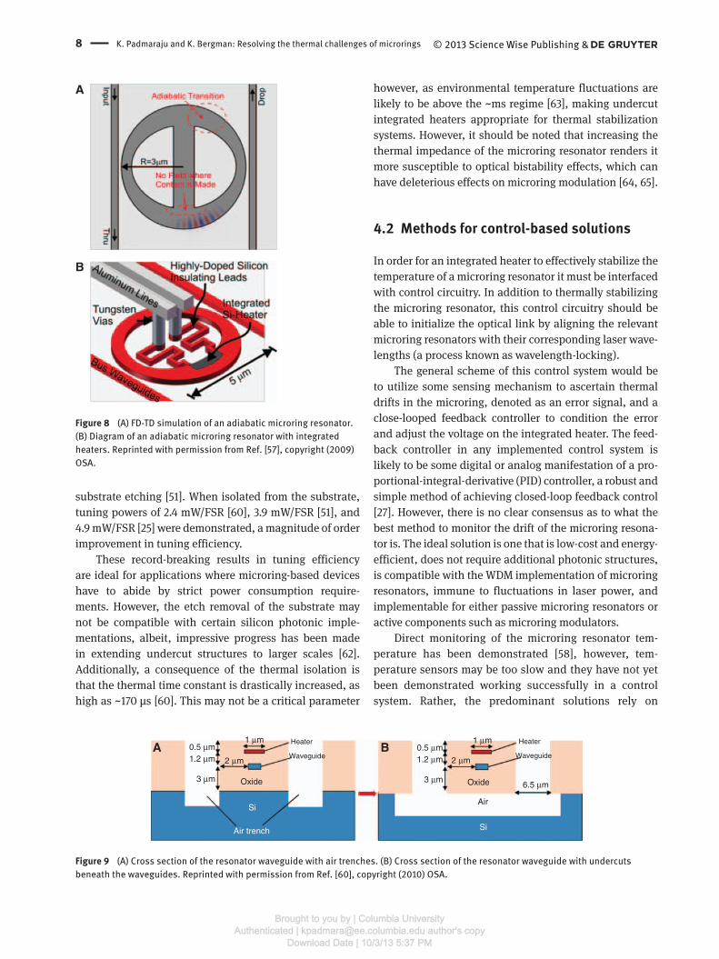
The cross-sections in Figure 7 , depicts the normal configuration for integrated heaters, whereby a thermally grown SiO 2 layer of ~1 µ m separates the metal heater from the silicon waveguide [15]. The separation between the heater and silicon waveguide is required to protect the optical mode ( Figure 7 A). The tuning efficiency is not optimal as a consequence of the separation, as the gener-ated heat has to diffuse from the point-like source of the heater down to the silicon waveguide ( Figure 7 B). While this configuration is the easiest to implement in fabrica-tion, demonstrated tuning efficiencies are limited, with most results ranging around ~100 mW/FSR [15, 52 – 54], and the best demonstration at ~42 mW/FSR with a tuning speed of 14 µ s [55]. These tuning efficiencies may be suf-ficient for some applications, but for the applications with the most stringent requirements on interconnect power consumption an improved tuning efficiency will be required. Demonstrations have shown that the tuning effi-ciency can be improved by either locating the integrated heater closer to the microring resonator or by improving the thermal isolation of the microring.
There is an inherent difficulty of locating the inte-grated heater closer to the microring resonator without causing the optical mode to incur additional scattering loss. A solution to resolving this problem is to utilize a
microdisk resonator (functionality equivalent to a micro-ring resonator) and place the integrated heater within the interior of the resonator. However, microdisk structures also support additional optical modes which corrupt the FSR of the resonator. The use of adiabatic microring reso-nators merges the benefits of microring and microdisk structures, allowing interior connections to the resonator while suppressing spurious optical modes and maintain-ing a small footprint [56]. Figure 8 A depicts the form factor of an adiabatic microring resonator, and the direct inte-gration of a heater within the resonator ( Figure 8 B). Lever-aging the intimate placement of the heater, tuning powers as low as ~20 mW/FSR with tuning speeds as fast as ~1 µ s were demonstrated [57]. Additionally, it was shown that adiabatic microring modulators could be fabricated [58]. Modulators with interior integrated heaters have been shown to be able to produce error-free 10 Gb/s modulation across a 60 K temperature tuning range, with comparable tuning efficiencies [59].
Another method to improve the tuning efficiency of integrated heaters is to increase the thermal isolation of microring resonators. Ordinarily, much of the heat gener-ated by the integrated heater is dissipated into the sur-rounding oxide and substrate. To prevent this, air trenches can be etched around the resonator structure, increasing its thermal isolation from the surrounding environment ( Figure 9 A). Using this technique, tuning powers of 21 mW/FSR with tuning time constants < 10 µ s were demon-strated [61].
Further improvements in tuning efficiency can be obtained by completely thermally isolating the resona-tor structure from the silicon substrate ( Figure 9 B) The particulars of the nanofabrication technique to achieve this physical isolation differ, and can utilize either topside silicon undercut-etching [25, 60], or backside
A 0.5
0.5
1.0
1.0 1.00 0 33
4
2
0
Heater
Metal heater Opticalwaveguide
mode
250
200
150
50
100
Distance (µm) Distance (µm)
Dis
tanc
e (µ
m)
Dis
tanc
e (µ
m)
Tem
pera
ture
(°K
)
1.5
0
B
Figure 7 Heater and waveguide design for thermal and optical efficiency: (A) the optical mode is separated from the heater to avoid absorption while (B) maintaining enough proximity to couple heat into the waveguide. Reprinted with permission from Ref. [15], copyright (2008) OSA.
© 2013 Science Wise Publishing &
Brought to you by | Columbia UniversityAuthenticated | [email protected] author's copy
Download Date | 10/3/13 5:37 PM
8 K. Padmaraju and K. Bergman: Resolving the thermal challenges of microrings
however, as environmental temperature fluctuations are likely to be above the ~ms regime [63], making undercut integrated heaters appropriate for thermal stabilization systems. However, it should be noted that increasing the thermal impedance of the microring resonator renders it more susceptible to optical bistability effects, which can have deleterious effects on microring modulation [64, 65].
4.2 Methods for control-based solutions
In order for an integrated heater to effectively stabilize the temperature of a microring resonator it must be interfaced with control circuitry. In addition to thermally stabilizing the microring resonator, this control circuitry should be able to initialize the optical link by aligning the relevant microring resonators with their corresponding laser wave-lengths (a process known as wavelength-locking).
The general scheme of this control system would be to utilize some sensing mechanism to ascertain thermal drifts in the microring, denoted as an error signal, and a close-looped feedback controller to condition the error and adjust the voltage on the integrated heater. The feed-back controller in any implemented control system is likely to be some digital or analog manifestation of a pro-portional-integral-derivative (PID) controller, a robust and simple method of achieving closed-loop feedback control [27]. However, there is no clear consensus as to what the best method to monitor the drift of the microring resona-tor is. The ideal solution is one that is low-cost and energy-efficient, does not require additional photonic structures, is compatible with the WDM implementation of microring resonators, immune to fluctuations in laser power, and implementable for either passive microring resonators or active components such as microring modulators.
Direct monitoring of the microring resonator tem-perature has been demonstrated [58], however, tem-perature sensors may be too slow and they have not yet been demonstrated working successfully in a control system. Rather, the predominant solutions rely on
A 0.5 µm1.2 µm
3 µm
0.5 µm1.2 µm
6.5 µm
Air
Si
Si
3 µm
2 µm 2 µm
1 µm 1 µm
Oxide Oxide
Heater Heater
Waveguide WaveguideB
Air trench
Figure 9 (A) Cross section of the resonator waveguide with air trenches. (B) Cross section of the resonator waveguide with undercuts beneath the waveguides. Reprinted with permission from Ref. [60], copyright (2010) OSA.
A
B
Figure 8 (A) FD-TD simulation of an adiabatic microring resonator. (B) Diagram of an adiabatic microring resonator with integrated heaters. Reprinted with permission from Ref. [57], copyright (2009) OSA.
substrate etching [51]. When isolated from the substrate, tuning powers of 2.4 mW/FSR [60], 3.9 mW/FSR [51], and 4.9 mW/FSR [25] were demonstrated, a magnitude of order improvement in tuning efficiency.
These record-breaking results in tuning efficiency are ideal for applications where microring-based devices have to abide by strict power consumption require-ments. However, the etch removal of the substrate may not be compatible with certain silicon photonic imple-mentations, albeit, impressive progress has been made in extending undercut structures to larger scales [62]. Additionally, a consequence of the thermal isolation is that the thermal time constant is drastically increased, as high as ~170 µ s [60]. This may not be a critical parameter
© 2013 Science Wise Publishing &
Brought to you by | Columbia UniversityAuthenticated | [email protected] author's copy
Download Date | 10/3/13 5:37 PM
K. Padmaraju and K. Bergman: Resolving the thermal challenges of microrings 9
indirectly monitoring drifts in the microring resonator. For instance, one example utilizes an infrared camera to image scattered light, however, this method will likely be difficult to scale and implement in a cost-effective and compact manner [66].
Several methods utilize the optical power of the signal to infer drifts in the microring resonator. It was shown that wavelength-locking and stabilization could be achieved by algorithmically searching for the point of minimum power transmission of a passive microring resonator [67]. While effective, it remains to be seen whether the FPGA-implementation can be translated to simple low-power circuitry, and additionally, the technique may be vulner-able to fabry-perot artifacts in the optical path.
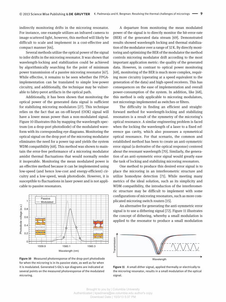
Additionally, it has been shown that monitoring the optical power of the generated data signal is sufficient for stabilizing microring modulators [27]. This technique relies on the fact that an on-off-keyed (OOK) signal will have a lower mean power than a non-modulated signal. Figure 10 illustrates this by mapping the wavelength spec-trum (on a drop-port photodiode) of the modulated wave-form with its corresponding eye diagrams. Monitoring the optical signal on the drop port of the microring modulator eliminates the need for a power tap and yields the system WDM compatibility [68]. This method was shown to main-tain the error-free performance of a microring modulator amidst thermal fluctuations that would normally render it inoperable. Monitoring the mean modulated power is an effective method because it can be implemented using low-speed (and hence low-cost and energy-efficient) cir-cuitry and a low-speed, weak photodiode. However, it is susceptible to fluctuations in laser power and is not appli-cable to passive resonators.
1559.9 1560.1 1560.3
Wavelength (nm)
0
0.2
0.4
0.6
0.8
1
Pho
todi
ode
volta
ge (
a.u.
)
PassiveModulated
Figure 10 Measured photoresponse of the drop-port photodiode for when the microring is in its passive state, as well as for when it is modulated. Generated 5-Gb/s eye diagrams are indicated at several points on the measured photoresponse of the modulated microring.
A departure from monitoring the mean modulated power of the signal is to directly monitor the bit-error-rate (BER) of the generated data stream [69]. Demonstrated results showed wavelength locking and thermal stabiliza-tion of the modulator over a range of 32 K. By directly moni-toring and optimizing the BER of the modulator the method controls microring modulator drift according to the most important application metric: the quality of the generated data. However, in contrast to optical power monitoring [68], monitoring of the BER is much more complex, requir-ing more circuitry (operating at a speed equivalent to the generation of the data) and high-speed receivers. This has consequences on the ease of implementation and overall power-consumption of the system. In addition, like [68], this method is only applicable to microring modulators, not microrings implemented as switches or filters.
The difficulty in finding an efficient and straight-forward method for wavelength-locking and stabilizing resonators is a result of the symmetry of the microring ’ s optical resonance. A similar engineering problem is faced when the locking the wavelength of a laser to a fixed ref-erence gas cavity, which also possesses a symmetrical optical resonance. For that scenario, the common and established method has been to create an anti-symmetric error signal (a derivative of the optical response) centered about the resonant wavelength [70]. Similarly, the genera-tion of an anti-symmetric error signal would greatly ease the task of locking and stabilizing microring resonators.
One method to produce this desired error signal is to place the microring in an interferometric structure and utilize homodyne detection [71]. While meeting many metrics of the ideal solution, such as its simplicity and WDM compatibility, the introduction of the interferomet-ric structure may be difficult to implement with some configurations of microring resonators, such as more com-plicated microring switch routers [15].
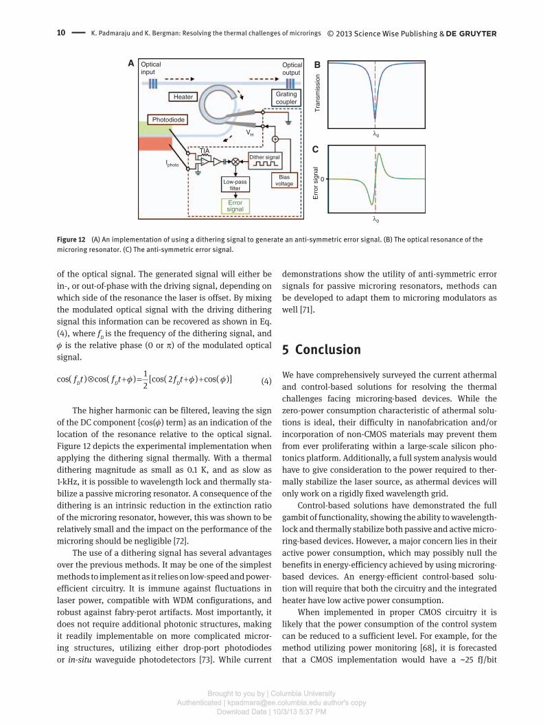
An alternative for generating the anti-symmetric error signal is to use a dithering signal [72]. Figure 11 illustrates the concept of dithering, whereby a small modulation is applied to the resonator to produce a small modulation
Tra
nsm
issi
on
Wavelength
Figure 11 A small dither signal, applied thermally or electrically to the microring resonator, results in a small modulation of the optical signal.
© 2013 Science Wise Publishing &
Brought to you by | Columbia UniversityAuthenticated | [email protected] author's copy
Download Date | 10/3/13 5:37 PM
10 K. Padmaraju and K. Bergman: Resolving the thermal challenges of microrings
of the optical signal. The generated signal will either be in-, or out-of-phase with the driving signal, depending on which side of the resonance the laser is offset. By mixing the modulated optical signal with the driving dithering signal this information can be recovered as shown in Eq. (4), where f D is the frequency of the dithering signal, and φ is the relative phase (0 or π ) of the modulated optical signal.
1cos( ) cos( ) [cos( 2 ) cos( )]2D D Df t f t f tφ φ φ⊗ + = + +
(4)
The higher harmonic can be filtered, leaving the sign of the DC component { cos( φ ) term } as an indication of the location of the resonance relative to the optical signal. Figure 12 depicts the experimental implementation when applying the dithering signal thermally. With a thermal dithering magnitude as small as 0.1 K, and as slow as 1-kHz, it is possible to wavelength lock and thermally sta-bilize a passive microring resonator. A consequence of the dithering is an intrinsic reduction in the extinction ratio of the microring resonator, however, this was shown to be relatively small and the impact on the performance of the microring should be negligible [72].
The use of a dithering signal has several advantages over the previous methods. It may be one of the simplest methods to implement as it relies on low-speed and power-efficient circuitry. It is immune against fluctuations in laser power, compatible with WDM configurations, and robust against fabry-perot artifacts. Most importantly, it does not require additional photonic structures, making it readily implementable on more complicated micror-ing structures, utilizing either drop-port photodiodes or in-situ waveguide photodetectors [73]. While current
demonstrations show the utility of anti-symmetric error signals for passive microring resonators, methods can be developed to adapt them to microring modulators as well [71].
5 Conclusion We have comprehensively surveyed the current athermal and control-based solutions for resolving the thermal challenges facing microring-based devices. While the zero-power consumption characteristic of athermal solu-tions is ideal, their difficulty in nanofabrication and/or incorporation of non-CMOS materials may prevent them from ever proliferating within a large-scale silicon pho-tonics platform. Additionally, a full system analysis would have to give consideration to the power required to ther-mally stabilize the laser source, as athermal devices will only work on a rigidly fixed wavelength grid.
Control-based solutions have demonstrated the full gambit of functionality, showing the ability to wavelength-lock and thermally stabilize both passive and active micro-ring-based devices. However, a major concern lies in their active power consumption, which may possibly null the benefits in energy-efficiency achieved by using microring-based devices. An energy-efficient control-based solu-tion will require that both the circuitry and the integrated heater have low active power consumption.
When implemented in proper CMOS circuitry it is likely that the power consumption of the control system can be reduced to a sufficient level. For example, for the method utilizing power monitoring [68], it is forecasted that a CMOS implementation would have a ~25 fJ/bit
A Opticalinput
Opticaloutput
Gratingcoupler
Biasvoltage
0
λ0
λ0
Dither signal
Tra
nsm
issi
onE
rror
sig
nal
TIA
Iphoto
Low-passfilter
Errorsignal
-+
Photodiode
VH
Heater
C
B
Figure 12 (A) An implementation of using a dithering signal to generate an anti-symmetric error signal. (B) The optical resonance of the microring resonator. (C) The anti-symmetric error signal.
© 2013 Science Wise Publishing &
Brought to you by | Columbia UniversityAuthenticated | [email protected] author's copy
Download Date | 10/3/13 5:37 PM
K. Padmaraju and K. Bergman: Resolving the thermal challenges of microrings 11
power consumption (at a 10 Gb/s data rate). CMOS imple-mentation of the dithering method [72] would require building further upon this circuitry, but likely keep power consumption below 100 fJ/bit. Similarly, it is forecasted that the BER monitoring method [69] would consume only 55 fJ/bit (at 10 Gb/s).
Of significant concern is the power consumption of the integrated heaters. If it is indeed required to tune microring resonators over a full FSR the integrated heaters would be the dominant source of power consump-tion in the optical link. However, current system designs suggest that such large tuning ranges are unnecessary. Advances in silicon photonic fabrication have been able to control wafer and etch tolerances to produce relatively evenly spaced WDM microring arrays [74]. In evenly channel-spaced WDM microring arrays, no microring will need to be initially tuned beyond one channel spacing
length. In addition, following large temperature swings, channel assignments can be reshuffled to minimize the aggregate tuning needed [21], potentially reducing the required power consumption of the integrated heaters to values < 100 fJ/bit (at 10 Gb/s) [69]. More accurate estimates of power consumption may only arrive with further progress in the development and implementation of control systems. However, another consideration that requires equal attention are the temperature parameters of the environment, specifically the magnitude and band-width of thermal fluctuations afflicting microring-based devices [63]. Better definition of these parameter-bounds will enable a more accurate assessment of the power-con-sumption of control systems.
Received May 13, 2013; accepted August 12, 2013
References [1] Krishnamoorthy AV, Ho R, Zheng X, Schwetman, H. Computer
systems based on silicon photonic interconnects. Proc IEEE 2009;97(7):1337 – 61.
[2] Urata R, Liu H, Lam C, Dashti P, Johnson C. Silicon photonics for optical access networks. Proc IEEE Group IV Photonics, San Diego, CA, 2012:207 – 9.
[3] Lee BG, Plouchart J, Rylyakov AV, Song JH, Doany FE, Schow CL. Passive photonics in an unmodified CMOS technology with no post-processing required. IEEE Photonic Tech L 2013;25(4):393 – 6.
[4] Dong P, Qian W, Liao S, Liang H, Kung CC, Feng NN, Shafiiha R, Fong J, Feng D, Krishnamoorthy AV, Asghari M. Low loss shallow-ridge silicon waveguides. Opt Express 2010;18(14):14474 – 9.
[5] Xu F, Poon AW. Silicon cross-connect filters using microring resonator coupled multimode-interference-based waveguide crossings. Opt Express 2008;16(12):8649 – 57.
[6] Green WMJ, Rooks MJ, Sekaric L, Vlasov YA. Ultra-compact, low RF power, 10 Gb/s silicon Mach-Zhender modulator. Opt Express 2007;15(25):17106 – 13.
[7] Cheung STS, Guan B, Djordjevic SS, Okamoto K, Yoo SJB. Low-loss and high contrast silicon-on-insulator (SOI) arrayed waveguide grating. Proc Conference on Lasers and Electro-Optics, San Jose, 2012.
[8] Grote RR, Padmaraju K, Driscoll JB, Souhan B, Bergman K, Osgood R. 10 Gb/s Error-free operation of all-silicon ion-implanted-waveguide photodiodes at 1.55 µ m. IEEE Photonic Tech L 2013;25(1):67 – 70.
[9] Assefa S, Xia F, Bedell SW, Zhang Y, Topuria T, Rice PM, Vlasov YA. CMOS-integrated high-speed MSM germanium waveguide photodetector. Opt Express 2010;18(5):4986 – 99.
[10] Xu Q, Fattal D, Beausoleil RG. Silicon microring resonators with 1.5- µ m radius. Opt Express 2008;16(6):4309 – 15.
[11] Xu Q, Schmidt B, Pradhan S, Lipson M. Micrometre-scale silicon electro-optic modulator. Nature 2005;435:325 – 7.
[12] Pantouvaki M, Yu H, Rakowski M, Christie P, Verheyen P, Lepage G, Van Hoovels N, Absil P, Van Campenhout J. Comparison of silicon ring modulators with interdigitated and lateral PN junctions. IEEE J Sel Top Quant 2013;19(2): Article ID: 7900308.
[13] Chen L, Lipson M. Ultra-low capacitance and high-speed germanium photodetectors on silicon. Opt Express 2009;17(10):7901 – 6.
[14] Biberman A, Lira HLR, Padmaraju K, Ophir N, Chan J, Lipson M, Bergman K. Broadband silicon photonic electrooptic switch for photonic interconnection networks. IEEE Photonic Tech L 2011;23(8):504 – 6.
[15] Sherwood-Droz N, Wang H, Chen L, Lee BG, Biberman A, Bergman K, Lipson M. Optical 4 × 4 hitless silicon router for optical Networks-on-Chip (NoC). Opt Express 2008;16(20):15915 – 22.
[16] Li G, Zheng X, Yao J, Thacker H, Shubin I, Luo Y, Raj K, Cunningham JE, Krishnamoorthy AV. 25Gb/s 1V-driving CMOS ring modulator with integrated thermal tuning. Opt Express 2011;19(21):20435 – 43.
[17] Xiao X, Xu H, Li X, Li Z, Chu T, Yu J, Yu Y. 60 Gbit/s Silicon modulators with enhanced electro-optical efficiency. Proc Optical Fiber Communication Conference, Anaheim, 2013.
[18] Lee BG, Small BA, Xu Q, Lipson M, Bergman K. Charac-terization of a 4 × 4 Gb/s parallel electronic bus to WDM optical link silicon photonic translator. IEEE Photonic Tech L 2007;19(7):456 – 8.
[19] Ophir N, Mountain D, Mineo C, Bergman K. Silicon photonic microring links for high-bandwidth-density, low-power chip I/O. IEEE Micro 2013;33(1):54 – 67.
[20] Ayazi A, Baehr-Jones T, Liu Y, Lim AEJ, Hochberg M. Linearity of silicon ring modulators for analog optical links. Opt Express 2012;20(12):13115 – 22.
[21] Georgas M, Leu J, Moss B, Sun C, Stojanovic V. Addressing link-level design tradeoffs for integrated photonics
© 2013 Science Wise Publishing &
Brought to you by | Columbia UniversityAuthenticated | [email protected] author's copy
Download Date | 10/3/13 5:37 PM
12 K. Padmaraju and K. Bergman: Resolving the thermal challenges of microrings
interconnects. Proc IEEE Custom Integrated Circuits Conference, 2011.
[22] Preston K, Sherwood-Droz N, Levy JS, Lipson M. Performance guidelines for WDM interconnects based on silicon microring resonators. Proc Conference on Lasers and Electro-Optics, 2011.
[23] Magdalena SN, Tao L, Xuan W, Robert RP. Tunable silicon microring resonator with wide free spectral range. Appl Phys Lett 2006;89: Article ID: 071110.
[24] Teng J, Dumon P, Bogaerts W, Zhang H, Jian X, Han X, Zhao M, Morthier G, Baets R. Athermal silicon-on-insulator ring resonators by overlaying a polymer cladding on narrowed waveguides. Opt Express 2009;17(17):14627 – 33.
[25] Fang Q, Song J, Luo X, Jia L, Yu M, Lo G, Liu Y. High efficiency ring-resonator filter with NiSi heater. IEEE Photonic Tech L 2012;24(5):350 – 2.
[26] Alipour P, Hosseini ES, Eftekhar AA, Momeni B, Adibi A. Athermal performance in high-Q polymer-clad silicon microdisk resonators. Opt Lett 2010;35(20):3462 – 4.
[27] Padmaraju K, Chan J, Chen L, Lipson M, Bergman K. Thermal stabilization of a microring modulator using feedback control. Opt Express 2012;20(27):27999 – 8008.
[28] Knights AP, Huante-Ceron E, Ackert J, Logan D, Wojcik G, Zhang F, Gubenko A, Mikhrin S. Comb-laser driven WDM for short reach silicon photonic based optical interconnection. Proc IEEE Group IV Photonic, San Diego, CA, 2012:210–2.
[29] Livshits D, Livshits D, Gubenko YA, Krestnikov I, Mikhrin S, Kovsh A, Wojcik G. Cost-effective WDM optical interconnects enabled by quantum dot comb lasers. Proc Optoelectronic Interconnects and Component Integration IX, Vol. 7606, San Francisco, CA, 2010.
[30] Levy JS, Saha K, Okawachi Y, Foster MA, Gaeta AL, Lipson M. High-performance silicon-nitride-based multiple-wavelength source. IEEE Photonic Tech L 2012;24(16):1375 – 7.
[31] Kokobun Y, Funato N, Takizawa M. Athermal waveguides for temperature-independent lightwave devices. IEEE Photonic Tech L 1993;5(11):1297 – 300.
[32] Raghunathan V, Ye W, Hu J, Izuhara T, Michel J, Kimerlin L. Athermal operation of Silicon waveguides: spectral, second order and footprint dependencies. Opt Express 2010;18(17):17631 – 9.
[33] Milosevic MM, Gardes FY, Thomson DJ, Mashanovich GZ. Temperature insensitive racetrack resonators for near infrared applications. Proc Optical Fiber Communication Conference, Los Angeles, 2012.
[34] Lee J-M, Kim D-J, Ahn H, Kim S-H, Park G. Temperature dependence of a silicon nanophotonic ring resonator with a polymeric overlayer. J Lightwave Technol 2007;25(8):2236 – 43.
[35] Zhou L, Kashiwagi K, Okamoto K, Scott RP, Fontaine NK, Ding D, Akella V, Yoo SJB. Towards athermal optically-interconnected computing system using slotted silicon microring resonators and RF-photonic comb generation. Appl Phys A 2009;95:1101 – 9.
[36] Li Q, Yegnanarayanan S, Soltani M, Alipour P, Adibi A. A temperature-insensitive third-order coupled-resonator filter for on-chip terabit/s optical interconnects. IEEE Photonic Tech L 2010;22(23):1768 – 70.
[37] Raghunathan V, Grillanda S, Singh V, Canciamilla A, Morichetti F, Agarwal A, Michel J, Melloni A, Kimerling LC. Trimming of athermal silicon resonators. Proc Integrated
Photonics Research, Silicon and Nanophotonics, Colorado Springs, CO, 2012.
[38] Qiu F, Yu F, Spring AM, Yokoyama S. Athermal silicon nitride ring resonator by photobleaching of disperse red 1-doped poly(methyl methacrylate) polymer. Opt Lett 2012;37(19):4086 – 8.
[39] Zhou L, Okamoto K, Yoo SJB. Athermalizing and trimming of slotted silicon microring resonators with UV-sensitive PMMA upper-cladding. IEEE Photonic Tech L 2009;21(17):1175 – 7.
[40] Raghunathan V, Izuhara T, Michel J, Kimerling L. Stability of polymer-dielectric bi-layers for athermal silicon photonics. Opt Express 2012;20(14):16059 – 66.
[41] Shang K, Djordjevic SS, Li J, Liao L, Basak J, Liu H-F, Ben Yoo SJ. CMOS-compatible titanium dioxide deposition for athermal-ization of silicon photonic waveguides. Proc Conference on Lasers and Electro-Optics, San Jose, 2013.
[42] Zhu S, Lo GQ, Xie J, Kwong DL. Towards athermal nanoplasmonic resonators based on Cu-TiO2-Si hybrid plasmonic waveguide. Proc Optical Fiber Communication Conference, Anaheim, 2013.
[43] Djordjevic SS, Shang K, Guan B, Cheung ST, Liao L, Basak J, Liu HF, Yoo SJ. CMOS-compatible, athermal silicon ring modulators clad with titanium dioxide. Opt Express 2013;21(12):13958 – 68.
[44] Alipour P, Atabaki AH, Eftekhar AA, Adibi A. Athermal performance in titania-clad microresonators on SOI. Proc Frontiers in Optics, Rochester, NY, 2010.
[45] Uenuma M, Mooka T. Temperature-independent silicon waveguide optical filter. Opt Lett 2009;34(5):599 – 601.
[46] Guha B, Gondarenko A, Lipson M. Minimizing temperature sensitivity of silicon Mach-Zhender interferometers. Opt Express 2010;18(3):1879 – 87.
[47] Guha B, Kyotoku BBC, Lipson M. CMOS-compatible athermal silicon microring resonators. Opt Express 2010;18(4):3487 – 93.
[48] Guha B, Preston K, Lipson M. Athermal silicon microring electro-optic modulator. Opt Lett 2012;37(12):2253 – 5.
[49] Manipatruni S, Dokania RK, Schmidt B, Sherwood-Droz N, Poitras CB, Apsel AB, Lipson M. Wide temperature range operation of micrometer-scale silicon electro-optic modulators. Opt Lett 2008;33(19):2185 – 7.
[50] Li C, Bai R, Shafik A, Tabasy EZ, Tang G, Ma C, Chen C-H, Peng Z, Fiorentino M, Chiang P, Palermo S. A ring-resonator-based silicon photonics transceiver with bias-based wavelength stabilization and adaptive-power-sensitivity receiver. Proc International Solid-State Circuits Conference, San Francisco, 2013.
[51] Cunningham JE, Shubin I, Zheng X, Pinguet T, Mekis A, Luo Y, Thacker H, Li G, Yao J, Raj K, Krishnamoorthy AV. Highly-efficient thermally-tuned resonant optical filters. Opt Express 2010;18(18):19055 – 63.
[52] Ng H-Y, Wang MR, Li D, Wang X, Martinez J, Panepucci RR, Pathak K. 4 × 4 wavelength-reconfigurable photonic switch based on thermally tuned microring resonators. Opt Eng 2008;47: Article ID: 044601.
[53] Geng M, Jia L, Zhang L, Yang L, Chen P, Wang T, Liu Y. Four-channel reconfigurable optical add-drop multiplexer based on photonic wire waveguide. Opt Express 2009;17(7):5502 – 16.
[54] Yu H, Pantouvaki M, Dwivedi S, Verheyen P. Compact thermally tunable silicon racetrack modulators based on an asymmetric waveguide. IEEE Photonic Tech L 2013;25(2):159 – 62.
© 2013 Science Wise Publishing &
Brought to you by | Columbia UniversityAuthenticated | [email protected] author's copy
Download Date | 10/3/13 5:37 PM
K. Padmaraju and K. Bergman: Resolving the thermal challenges of microrings 13
[55] Gan F, Barwicz T, Popovic MA, Dahlem MS, Holzwarth CW, Rakich PT, Smith HI, Ippen EP, Kartner FX. Maximizing the thermo-optic tuning range of silicon photonic structures. Proc Photonics in Switching, San Francisco, CA, 2007:67 – 8.
[56] Watts MR. Adiabatic microring resonators. Opt Lett 2010;35(19):3231 – 3.
[57] Watts MR, Zortman WA, Trotter DC, Nielson GN, Luck DL, Young RW. Adiabatic resonant microrings (ARMs) with directly integrated thermal microphotonics. Proc Conference on Lasers and Electro-optics, 2009.
[58] DeRose CT, Watts MR, Trotter DC, Luck DL, Nielson GN, Young RW. Silicon microring modulator with integrated heater and temperature sensor for thermal control. Proc Conference on Lasers and Electro-optics, 2010.
[59] Zortman WA, Lentine AL, Trotter DC, Watts MR. Integrated CMOS compatible low power 10Gbps silicon photonic heater-modulator. Proc Optical Fiber Communication Conference, 2012.
[60] Dong P, Qian W, Liang H, Shafiiha R, Feng NN, Feng D, Zheng X, Krishnamoorthy AV, Asghari M. Thermally tunable silicon racetrack resonators with ultralow tuning power. Opt Express 2010;18(19):20298 – 304.
[61] Dong P, Qian W, Liang H, Shafiiiha R, Feng NN, Feng D, Zheng X, Krishnamoorthy AV, Asghari M. Low power and compact reconfigurable multiplexing devices based on silicon microring resonators. Opt Express 2010;18(10):9852 – 8.
[62] Shubin I, Li G, Zheng X, Luo Y, Thacker H, Yao J, Park N, Krishnamoorthy AV, Cunningham JE Integration, processing and performance of low power thermally tunable CMOS-SOI WDM resonators. Opt and Quant Electron 2012;44(12):589 – 604.
[63] Chen Y-H, Sun C, Stojanovic V. Scalable electrical-optical thermal simulator for multicores with optical interconnects. Proc IEEE Optical Interconnects, Santa Fe, NM, 2013.
[64] Zheng X, Luo Y, Li G, Shubin I, Thacker H, Yao J, Raj K, Cunningham JE, Krishnamoorthy AV. Enhanced optical bistability from self-heating due to free carrier absorption
in substrate removed silicon ring modulators. Opt Express 2012;20(10):11478 – 86.
[65] Li Q, Ophir N, Xu L, Padmaraju K, Chen L, Lipson M, Bergman K. Experimental characterization of the optical-power upper bound in a silicon microring modulator. Proc IEEE Optical Interconnects Conference, Santa Fe, 2012.
[66] Qiu C, Shu J, Li Z, Zhang X, Xu Q. Wavelength tracking with thermally controlled silicon resonators. Opt Express 2011;19(6):5143 – 8.
[67] Timurdogan E, Biberman A, Trotter DC, Sun C, Moresco M, Stojanovic V, Watts MR. Automated wavelength recovery for microring resonators. Proc Conference on Lasers and Electro-optics, San Jose, 2012.
[68] Padmaraju K, Logan DF, Zhu X, Ackert JJ, Knights AP, Bergman K. Integrated thermal stabilization of a microring modulator. Opt Express 2013;21(12):14342 – 50.
[69] Zortman WA, Lentine AL, Trotter DC, Watts MR. Bit error rate monitoring for active wavelength control of silicon microphotonic resonant modulators. IEEE Micro 2013;33(1):42 – 52.
[70] Hansch TW, Couillaud B. Laser frequency stabilization by polarization spectroscopy of a reflecting reference cavity. Opt Commun 1980;35(3):441 – 4.
[71] Cox JA, Trotter DC, Starbuck AL. Integrated control of silicon-photonic micro-resonator wavelength via balanced homodyne locking. Proc IEEE Optical Interconnects Conference, Santa Fe, 2013.
[72] Padmaraju K, Logan DF, Ackert JJ, Knights AP, Bergman K. Microring resonance stabilization using thermal dithering. Proc IEEE Optical Interconnects, Santa Fe, NM, 2013.
[73] Logan DF, Velha P, Sorel M, De La Rue RM, Jessop PE, Knights AP. Monitoring and tuning micro-ring properties using defect-enhanced silicon photodiodes at 1550 nm. IEEE Photonic Tech L 2011;24(4):261 – 3.
[74] Krishnamoorthy AV, Zheng X, Li G, Yao J, Pinguet T, Mekis A, Thacker H, Shubin I, Luo Y, Raj K, Cunningham JE. Exploiting CMOS manufacturing to reduce tuning requirements for resonant optical devices. IEEE Photonic J 2011;3(3):567 – 79.
© 2013 Science Wise Publishing &
Brought to you by | Columbia UniversityAuthenticated | [email protected] author's copy
Download Date | 10/3/13 5:37 PM
Nanophotonics 2013 | Volume x | Issue x
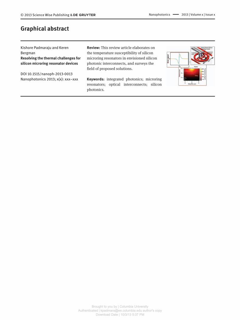
Kishore Padmaraju and Keren BergmanResolving the thermal challenges for silicon microring resonator devices
DOI 10.1515/nanoph-2013-0013Nanophotonics 2013; x(x): xxx–xxx
Review: This review article elaborates on the temperature susceptibility of silicon microring resonators in envisioned silicon photonic interconnects, and surveys the field of proposed solutions.
Keywords: integrated photonics; microring resonators; optical interconnects; silicon photonics.
Graphical abstract
© 2013 Science Wise Publishing &
Brought to you by | Columbia UniversityAuthenticated | [email protected] author's copy
Download Date | 10/3/13 5:37 PM