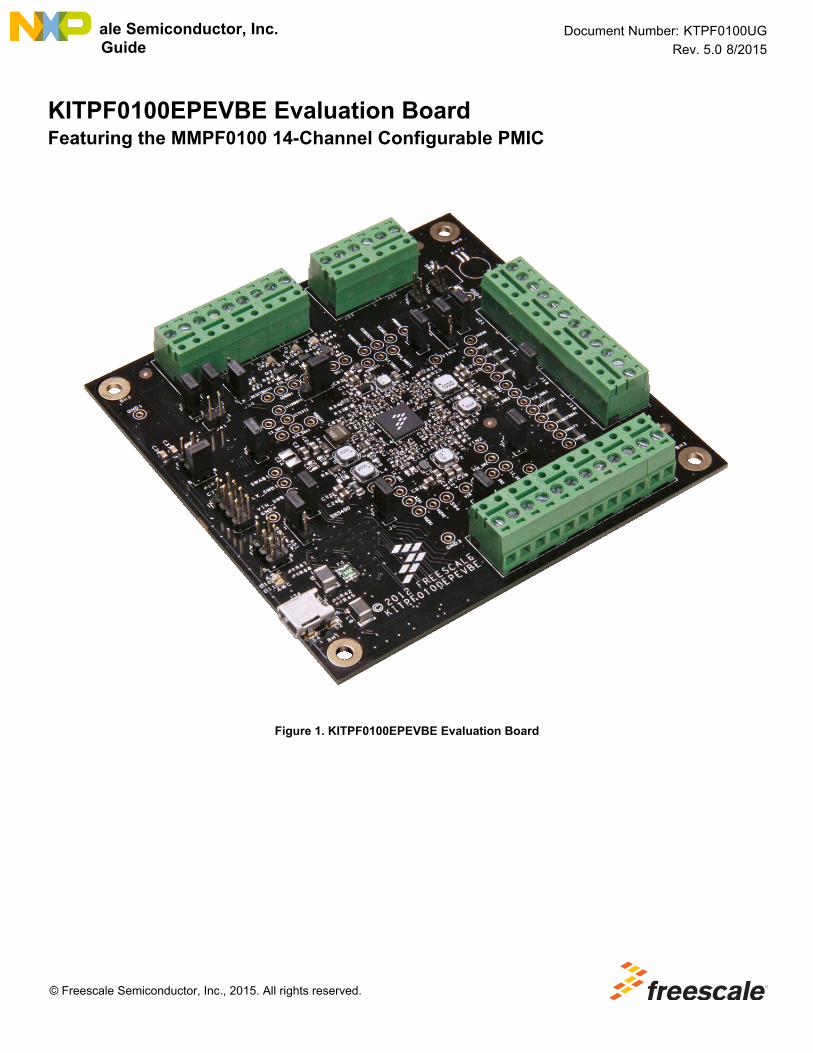
kitpf0100epevbe evaluation board
TRANSCRIPT
Freescale Semiconductor, Inc.User’s Guide
© Freescale Semiconductor, Inc., 2015. All rights reserved.
Document Number: KTPF0100UG
Rev. 5.0 8/2015
KITPF0100EPEVBE Evaluation BoardFeaturing the MMPF0100 14-Channel Configurable PMIC
Figure 1. KITPF0100EPEVBE Evaluation Board

KTPF0100UG Rev. 5.02 Freescale Semiconductor, Inc.
Contents
1 Important Notice . . . . . . . . . . . . . . . . . . . . . . . . . . . . . . . . . . . . . . . . . . . . . . . . . . . . . . . . . . . . . . . . . . . . . . . . . . . . . . 3
2 Getting Started . . . . . . . . . . . . . . . . . . . . . . . . . . . . . . . . . . . . . . . . . . . . . . . . . . . . . . . . . . . . . . . . . . . . . . . . . . . . . . . 4
3 Introduction . . . . . . . . . . . . . . . . . . . . . . . . . . . . . . . . . . . . . . . . . . . . . . . . . . . . . . . . . . . . . . . . . . . . . . . . . . . . . . . . . . 4
4 KITPF0100EPEVBE Features . . . . . . . . . . . . . . . . . . . . . . . . . . . . . . . . . . . . . . . . . . . . . . . . . . . . . . . . . . . . . . . . . . . 4
5 MMPF0100 Features . . . . . . . . . . . . . . . . . . . . . . . . . . . . . . . . . . . . . . . . . . . . . . . . . . . . . . . . . . . . . . . . . . . . . . . . . . 5
6 Hardware/Software Requirements . . . . . . . . . . . . . . . . . . . . . . . . . . . . . . . . . . . . . . . . . . . . . . . . . . . . . . . . . . . . . . . . 5
7 Hardware Configuration . . . . . . . . . . . . . . . . . . . . . . . . . . . . . . . . . . . . . . . . . . . . . . . . . . . . . . . . . . . . . . . . . . . . . . . . 6
8 Evaluation Board Schematic . . . . . . . . . . . . . . . . . . . . . . . . . . . . . . . . . . . . . . . . . . . . . . . . . . . . . . . . . . . . . . . . . . . . . 7
9 Hardware Description . . . . . . . . . . . . . . . . . . . . . . . . . . . . . . . . . . . . . . . . . . . . . . . . . . . . . . . . . . . . . . . . . . . . . . . . . 11
10 KITPF0100EPEVBE Board Layout . . . . . . . . . . . . . . . . . . . . . . . . . . . . . . . . . . . . . . . . . . . . . . . . . . . . . . . . . . . . . . . 23
11 Bill of Materials . . . . . . . . . . . . . . . . . . . . . . . . . . . . . . . . . . . . . . . . . . . . . . . . . . . . . . . . . . . . . . . . . . . . . . . . . . . . . . 29
12 References . . . . . . . . . . . . . . . . . . . . . . . . . . . . . . . . . . . . . . . . . . . . . . . . . . . . . . . . . . . . . . . . . . . . . . . . . . . . . . . . . 34
13 Revision History . . . . . . . . . . . . . . . . . . . . . . . . . . . . . . . . . . . . . . . . . . . . . . . . . . . . . . . . . . . . . . . . . . . . . . . . . . . . . 35

Important Notice
KTPF0100UG Rev. 5.0Freescale Semiconductor, Inc. 3
1 Important Notice Freescale provides the enclosed product(s) under the following conditions:
This evaluation kit is intended for use of ENGINEERING DEVELOPMENT OR EVALUATION PURPOSES ONLY. It is provided as a sample IC pre-soldered to a printed circuit board to make it easier to access inputs, outputs, and supply terminals. This evaluation kit may be used with any development system or other source of I/O signals by simply connecting it to the host MCU or computer board via off-the-shelf cables. Final device in an application will be heavily dependent on proper printed circuit board layout and heat sinking design as well as attention to supply filtering, transient suppression, and I/O signal quality.
The goods provided may not be complete in terms of required design, marketing, and or manufacturing related protective considerations, including product safety measures typically found in the end product incorporating the goods. Due to the open construction of the product, it is the user's responsibility to take any and all appropriate precautions with regard to electrostatic discharge. In order to minimize risks associated with the customers applications, adequate design and operating safeguards must be provided by the customer to minimize inherent or procedural hazards. For any safety concerns, contact Freescale sales and technical support services.
Should this evaluation kit not meet the specifications indicated in the kit, it may be returned within 30 days from the date of delivery and will be replaced by a new kit.
Freescale reserves the right to make changes without further notice to any products herein. Freescale makes no warranty, representation or guarantee regarding the suitability of its products for any particular purpose, nor does Freescale assume any liability arising out of the application or use of any product or circuit, and specifically disclaims any and all liability, including without limitation consequential or incidental damages. “Typical” parameters can and do vary in different applications and actual performance may vary over time. All operating parameters, including “Typical”, must be validated for each customer application by customer’s technical experts.
Freescale does not convey any license under its patent rights nor the rights of others. Freescale products are not designed, intended, or authorized for use as components in systems intended for surgical implant into the body, or other applications intended to support or sustain life, or for any other application in which the failure of the Freescale product could create a situation where personal injury or death may occur.
Should the Buyer purchase or use Freescale products for any such unintended or unauthorized application, the Buyer shall indemnify and hold Freescale and its officers, employees, subsidiaries, affiliates, and distributors harmless against all claims, costs, damages, and expenses, and reasonable attorney fees arising out of, directly or indirectly, any claim of personal injury or death associated with such unintended or unauthorized use, even if such claim alleges that Freescale was negligent regarding the design or manufacture of the part. Freescale™ and the Freescale logo are trademarks of Freescale Semiconductor, Inc. All other product or service names are the property of their respective owners. © Freescale Semiconductor, Inc. 2015

Getting Started
KTPF0100UG Rev. 5.04 Freescale Semiconductor, Inc.
2 Getting Started
2.1 Kit Contents/Packing List• Customer evaluation board KITPF0100EPEVBE• Warranty card and technical support brochure
3 Introduction The KITPF0100EPEVBE evaluation board supports the development and testing of the PF0100 PMIC, a member of Freescale’s i.MX6 family of application processors. The board provides access to all output voltage rails as well as control and signal pins through terminal block connectors. A single terminal block connector for the input power supply allows the user to supply the board with an external DC power supply to fully evaluate the performance of the device.
The KITPF0100EPEVBE comes with a non-programmed version of the PF0100 PMIC that is prepared to power up from the default sequence. However, an integrated control/fuse programming interface allows the customer to program the OTP/TBB (One Time Programmable/Try-Before-Buy) memory and also to select it as the default source for the power-up configuration. Likewise, the programming interface allows full control of the PF0100 through the I2C communication lines.
This document is intended to provide an overview of the KITPF0100EPEVBE evaluation board as well as detailed instruction for programming the PF0100 through its dedicated Graphic User Interface (GUI).
4 KITPF0100EPEVBE Features • Input voltage operation range from 3.1 V to 4.5 V• Output voltage supplies accessible through detachable terminal blocks
• Four to six independent buck converters• One 5.0 V boost regulator• Six general purpose LDO regulators• One DDR memory termination voltage reference• One VSRTC supply
• Coin cell support for “Try-Before-Buy” (TBB) mode• On/off push button support• Hardware configuration flexibility through various jumper headers and resistors• Integrated USB to I2C programming interface for full control/configuration
• Onboard OTP programming supply and control• Onboard PMIC control through the I2C register map• Fully featured programmer through J36 for external device control/programming
• On board connectors for interfacing with future evaluation/debug tools• Compact form factor (4 x 4 in2)

MMPF0100 Features
KTPF0100UG Rev. 5.0Freescale Semiconductor, Inc. 5
5 MMPF0100 FeaturesThe PF0100 Power Management Integrated Circuit (PMIC) provides a highly programmable/ configurable architecture with fully integrated power devices and minimal external components. With up to six buck converters, six linear regulators, RTC supply, and coin-cell charger, the PF0100 can provide power for a complete system, including applications processors, memory, and system peripherals, in a wide range of applications.
• Four to six buck converters, depending on configuration• Single/Dual phase/ parallel options• DDR termination tracking mode option
• Boost regulator to 5.0 V output• Six general purpose linear regulators• Programmable output voltage, sequence, and timing• OTP (One Time Programmable) memory for device configuration• Coin cell charger and RTC supply• DDR termination reference voltage• Power control logic with processor interface and event detection• Individually programmable ON, OFF, and Standby modes
Freescale analog ICs are manufactured using the SMARTMOS process, a combinational BiCMOS manufacturing flow which integrates precision analog, power functions, and dense CMOS logic on a single cost-effective die.
5.1 MC9S08JM60 FeaturesThe KITPF0100EPEVBE implements a Freescale MC9S08JM60 low-cost, high-performance 8-bit HCS08 microcontroller to interface via USB to I2C to control the main PMIC.
• 8-bit HCS08 Central Processing Unit (CPU)• Up to 24 MHz internal bus (48 MHz HCS08 core) frequency offering 2.7 to 5.5 V across temperature range of -40
to +85 °C • Support for up to 32 peripheral interrupt/reset sources
• On-Chip Memory• Up to 60 K flash read/program/erase over full operating voltage and temperature • Up to 4 K RAM• 256 Byte USB RAM
6 Hardware/Software Requirements
6.1 Hardware Requirements• Power supply:
• Output voltage range from 3.1 V to 4.5 V • Current capability from 3 to 5 A (current requirement is dependent on output loading)
• Supply to board connection cables (capable of withstanding up to 5.0 A current)• USB (male) to mini USB (male) communication cable.• USB-enabled computer.
6.2 Software Requirements• Windows XP or Windows 7 operating system

Hardware Configuration
KTPF0100UG Rev. 5.06 Freescale Semiconductor, Inc.
7 Hardware ConfigurationConnect the power supply and the USB communication cables as shown in Figure 2. Voltmeters are optional but it is recommended in order to accurately verify that each one of the output supplies is providing the correct voltage level.
Figure 2. Evaluation Board Setup
Note: The KITPF0100EPEVBE allows the selection of SW2 regulator output or an external 3.3 V LDO output as the VDDIO/I2C pull-up supply. By default, the SW2 regulator is the source for the VDDIO supply (J46 = 3-4). If the SW2 regulator is to be set below 3.0 V then switch the 3.3 V LDO connection to VDDIO (J46 = 1-2.)

Evaluation Board Schematic
KTPF0100UG Rev. 5.0Freescale Semiconductor, Inc. 7
8 Evaluation Board Schematic
Figure 3. KITPF0100EPEVBE LDO/Control Schematic Part 1
VGEN SENSE
1-2CLOSED
6.8mmPlace Bottom
6.8mm Leaded Place Top
VGEN1
VGEN2
VGEN3
VGEN4
VGEN5
VIN1
VIN3VREFDDR
VIN2
VGEN6
VSNVS
VGEN4
VGEN1
VGEN3
VGEN5
VGEN6
VGEN1
VGEN2
VGEN3
VGEN4
VGEN5
VGEN6
VSNVS
VGEN2
GND
GND
GND
VREFDDR
GND
VSNVS
VGEN1
VGEN2
VGEN3
VGEN4
VGEN5
VGEN6
VIN
VSNVS
SW3A
SW3B
3V3
VGEN1
VGEN2
VGEN3
VGEN4
VGEN5
VGEN6
VSNVS
SW2
SW2
SW2
3V3
C440.1UF
VGEN3DNP
J16
SUBASSY_TB_3x1
123
VGEN1DNP
MMPF0100NPEP
U1B
VGEN116
VGEN218
VIN340
VHALF29
VIN117
VGEN641
VINREFDDR30
VREFDDR31
VSNVS43
VGEN326
VGEN428
VIN227
LICELL42
VGEN539
R200 DNP
R240 DNP
VGEN4DNPC401.0UF
C432.2UF
J19
SUBASSY_TB_3x1
123R270 DNP
R230 DNP
VGEN6DNP
R86
0
DNP
+-
BAT2BK-879
DNP
13
2
C414.7uF
VREFDDR1DNP
C450.1UF
J21
SUBASSY_TB_3x1
123
C470.47uF
C42 2.2UF
J18
SUBASSY_TB_3x1
123
VGEN5DNP
R220
BAT1
LICELL
12
C354.7uF
C460.22uF
VHALF1DNP
C38 2.2UF
R260
R250
C34 2.2UF
VSNVS1DNPC84
1.0UF
J20
HDR 1X3
123
VGEN2DNP
R210
VINREFDDR1DNP
VDD OTPVDDOTP
VCOREDIG
VDDOTPIN
VDDOTPIN
C3910.0uF
C3710.0uF
C3610.0uF
J17HDR 2X3
12
34 6
5
R79
100K
VIN SENSE
VIN2
VIN3
VIN1
C50
1.0UF
VIN2
DNP
VIN3
DNP
VIN1
DNP
C48
1.0UF
C49
1.0UFGND
PVIN
INPUT SUPPLIES
CLOSEDCLOSEDSWVIN
VINPVIN SWVINSWVIN
J40
HDR 1X2 TH12J25
SUBASSY_TB_3x1
123
J27
HDR 1X2 TH12
J41
HDR 1X2 TH
12
VCOREDIG
PVIN
R8027KDNP
C852.2UFDNP
U7
MIC5205DNP
IN1
GND2
ADJ4
EN3
OUT5R83 0
DNPR81
470KDNPC86
470PFDNP
R82 0
DNP
STANDBY
VSNVS
R29100K
C871.0UF
J24
HD
R 1
X2 T
H
12
2-3 CLOSED
CLOSED
VCOREDIG
VCOREREF
VCORE
VDDOTP
ICTEST
VDDIO
VIN
PVIN
VSNVS
PVINPVIN
MCU_SDAMCU_SCL
PWRON
STANDBY
INTB
RESETBMCU
SDWNB
3V3
SW23V3
C511.0UF
VDDOTP1DNP
C56
0.1UF
VDDIO1DNP
J22
HDR 1X31 2 3
CONSUMER/INDUSTRIAL
MMPF0100NPEP
U1A
ICTEST5
INTB1
RESETBMCU3
SCL54
SDA53
SDWNB2
STANDBY4
VCOREDIG51
VCOREREF52
VDDIO55
VDDOTP47
PWRON56
VCORE49
GNDREF48
VIN50
SW1FSMSM1 2
J47
HDR 1X2 TH12
VIN_SENSE1
DNP
PWRON1DNP
R3110.0K
J26
HDR 1X2 TH12
J46
HDR 2X2
1 23 4
C541.0UF
R350
SDA1DNP
R3210.0K
VCORE1DNP
C521.0UF
STANDBY1DNP
R374.7K
SDWNB1DNP
C551.0UFDNP
C530.22uF
INTB1DNP
R28
1M
SCL1DNP
VCOREREF1DNP
R364.7K
RESETBMCU1DNP
J45
HDR 2X2
1 23 4
VCOREDIG1
DNPR30
10.0K
ICTEST1
DNP
I2C Terminal Blocks
VDDIOGND
MCU_SDAMCU_SCL
J33
SUB_TB_2x1
12
J31
SUB_TB_2x1
12
INTBSDWNBRESETBMCU
STANDBYPWRON
GND
J32
SUBASSY_TB_3x1
123
J29
SUBASSY_TB_3x1
123
Mounting Holes
GND's
GND
BH4
MTG
GND3
DNP
BH2
MTG
GND5
DNP
BH3
MTG
BH1
MTG
GND1
DNP
GND6
DNP
GND2
DNP
GND4
DNP
VGEN1VGEN2VGEN3VGEN4
VGEN5VGEN6
VSNVSVREFDDR
J43
CON_2X10
1234
6 57891011121314151617181920
SWVINPVIN
STANDBY PWRONINTBSDWNBRESETBMCUSWBSTVDDIOMCU_SCLMCU_SDA
J44
CON_2X10
1234
6 57891011121314151617181920
RESETINDICATOR
SHUTDOWNINDICATOR
INTERRUPTINDICATOR
PVIN PVIN PVIN
PVIN
RESETBMCU
INTB PW
RO
N
D2LED Red
AC
R38200 OHM
12
R39200 OHM
12
Q3FDV302P
1
32
D3LED Red
AC
R40200 OHM
12
Red
Grn
D4 LED_RED-GRN
42 1
3
Q2FDV302P
1
32
R69200 OHM
12
G
D
SG
S
D
Q1
FDC6327C
2
6
15
4
3

Evaluation Board Schematic
KTPF0100UG Rev. 5.08 Freescale Semiconductor, Inc.
Figure 4. KITPF0100EPEVBE LDO/Control Schematic Part 2
RESETINDICATOR
RESERVEDINDICATOR
INTERRUPTINDICATOR
Mounting Holes GND's
I2C Terminal BlocksInterface Terminal BlocksLDO Terminal Blocks
HOT PLUG WORKAROUND
GND
VGEN1
VGEN2
VGEN3
VGEN4
VGEN5
VGEN6
VSNVSGND
INTBSDWNBRESETBMCU
STANDBYPWRON
GND
GND
GND
VREFDDR
GND
VDDIOGND
VCOREDIG
PVIN PVIN PVIN
PVIN
PVIN
SWVINPVIN
RESETBMCU
MCU_SDA
INTB
MCU_SCL
VGEN1VGEN2VGEN3VGEN4
VGEN5VGEN6
VSNVSVREFDDR
STANDBY PWRONINTBSDWNBRESETBMCUSWBSTVDDIOMCU_SCLMCU_SDA
SW1CSW1C
SW1AB SW1AB
SW4 SW4
SW2SW2SW3BSW3B
SW3ASW3A
D2LED Red
AC
J16
SUBASSY_TB_3x1
123
BH4
MTG
R8027K
R84 0
DNP
J19
SUBASSY_TB_3x1
123
R38200 OHM
12
GND3
DNP
R39200 OHM
12
Q3FDV302P
1
32
C852.2UFDNP
BH2
MTG
D3LED Red
AC
J21
SUBASSY_TB_3x1
123
J42
HDR_2X10DNP
1234
6 57891011121314151617181920
R40200 OHM
12
U7
MIC5205
IN1
GND2
ADJ4
EN3
OUT5R83 0
DNP
J18
SUBASSY_TB_3x1
123
J32
SUBASSY_TB_3x1
123
GND5
DNP
R81470K
J44
HDR_2X10DNP
1234
6 57891011121314151617181920
J33
SUB_TB_2x1
12
BH3
MTG
Red
Grn
D4 LED_RED-GRN
42 1
3
BH1
MTG
Q2FDV302P
1
32
GND1
DNP
GND6
DNP
GND2
DNP
J31
SUB_TB_2x1
12
GND4
DNP
J43
HDR_2X10DNP
1234
6 57891011121314151617181920
C86
470PF
R69200 OHM
12
G
D
SG
S
D
Q1
FDC6327C
2
6
15
4
3
J29
SUBASSY_TB_3x1
123
R82 0
DNP

Evaluation Board Schematic
KTPF0100UG Rev. 5.0Freescale Semiconductor, Inc. 9
Figure 5. KITPF0100EPEVBE Switching Regulators Schematic
CLOSED
CLOSED
CLOSED
CLOSED
CLOSED
CLOSED
CLOSED
CLOSED
SW3AFB
SW1ABFB
SW1BIN SW3BIN
SW3BLX
SW3ALX
SW1CLX
SW2LX
SWBSTIN
SW1CFB
SW1CFB
SW1VSSSNS
SW2LX
SW2FB
SW3AFB
SW2FB
SW4LX
SW4LX
SW4FB
SW1BLX
SW4FB
SW1ALX
SW3BFB
SW4IN
SWBSTFB
SWBSTFB
SW1ABFB
SW1CIN
SWBSTLX
SW1CLX
SW1BLX
SW1ALX
SW3BLX
SW3BFB
SW3ALX
SWVIN
SWVIN
SWVIN
SWVIN
SWVIN
SWVIN
SWVIN
SWVIN
SW2
SW4
SW1AB
SW3A
SW3B
SWBST
SW1C
C3322UF
R17
0.001DNP
LX_SWB1DNP
L1 2.2UH1 2
L7
1uH1 2
J9
HDR 1X2 TH
12
J8
SUB_TB_2x1
12
L8
1uH1 2
SW4DNP
C70.1uF
J3
HDR 1X2 TH
12
C150.01UF
C1810UF
C3122UF
C20
2.2UF
J5
HDR 1X2 TH
12
C8322UF
LX_SWA1DNP
R21.0
DNP
L4
1uH1 2
R1
0.001
VIN_SWA1DNP
VIN_SWC1
C100.1UF
C2922UF
C134.7uF
R70.001DNP
VIN_SW2
C140.1UF
J2
HDR 1X2 TH
12
C1622UF
R70
0.001DNP
C3222UF
C54.7uF
SWB3DNP
J12
SUB_TB_2x1
12
C124.7uF
C21
22UF
C3022UF
SWA3
DNP
VIN_SWB1
C20.1UF
VIN_SWBST1DNP
VSWBST1DNP
C2822UF
D1
MBR120LSFT1G
A C
C2522UF
R4
0.001
L5
1uH1 2
C23
22UFDNP
C11
0.1UF
L3
1uH1 2
C94.7uF
LX_SWBST1DNP
R16
0.001
R85 0
J6
HDR 1X2 TH
12
C2622UF
J11
SUB_TB_2x1
12
R3
0.001
C14.7uF
C84.7uF
LX_SWA3DNP
LX_SW2DNP
R60.001
J10
SUB_TB_2x1
12
VIN_SWA3 DNP
LX_SW4DNP
C24
22UFDNP
R90.001DNP
LX_SWB3DNP
VIN_SWB3 DNP
J13
SUB_TB_2x1
12
J4
HDR 1X2 TH
12
SW2DNP
R11
0.001
VIN_SW4 DNP
J14
SUB_TB_2x1
12
J15
SUB_TB_2x1
12
R100.001DNP
R8
0.001
C19
0.1uF
C2722UF
J1
HDR 1X2 TH
12
J7
HDR 1X2 TH
12
SWC1
DNP
C171000pF DNP
C22
22UF
C40.1uF
C60.1UF
LX_SWC1DNP
SWAB1
DNP
L2
1uH
1 2
L6
1UH1 2
C34.7uF
C8222UF
MMPF0100NPEPU1C
SW1CIN12
SW1VSSSNS14
SW2IN_123
SW3AFB38
SW3AIN37
SW3ALX36
SW3BFB33
SW3BIN34
SW3BLX35
SW3VSSSNS32
SW4FB19
SW4IN20
SWBSTFB44
SWBSTIN45
SWBSTLX46
SW1AIN7
SW1ALX8
SW1BIN10
SW1BLX9
SW1CFB13
SW1CLX11
SW1FB6
SW2FB25
SW2LX22
SW4LX21
EP
GN
D57
GN
DR
EF1
15
SW2IN_224

Evaluation Board Schematic
KTPF0100UG Rev. 5.010 Freescale Semiconductor, Inc.
Figure 6. KITPF0100EPEVBE Control/Programming Interface Schematic
Programming Interface
USB Connector Type A
BDM Programmer
ESD PROTECTION
Crystal
MAIN ICMC9S08JM60
LED INDICATORS
8V - Boost ConverterCLOSED
LDO REGULATOR 3.3V
VOUT = 1.242 X ( (R2/R1) + 1) = 3.3V
R2 = ((VOUT/1.242) -1) X R1
R1R2
Place on Bottom
Place on Bottom
Place on Bottom
Place on Bottom
Place on Bottom
D-D+G
VVUSBDN
USBDP
USB_PWRRST_JM60
MC
U_S
CL
MC
U_S
DA
ID1
ID0
EXTAL_JM60
XTAL_JM60
EXTAL_JM60XTAL_JM60
BKGD_JM60
BSTENVUSBEN
3V3ENVPGMEN
LRONLGON
ID0ID1
USBDNUSBDP
VUSB33
VUSB33RST_JM60
BKGD_JM60
LGON LRON
PWRON
MCU_SCL
BSTEN
BSTDNBSTUP
VPGMEN
BSTUPBSTDN
VDDOTPIN
3V3
3V3EN
VIN_USB
GPIO1GPIO2
MCU_SDA
VUSBEN
VIN_USB
VDDOTPIN_SNS
VDDOTPIN_SNS
USB_PWR
USB_PWR
USB_PWR
USB_PWRUSB_PWR
0
0
0
PVIN
0
0
0
0
0
VDDOTPIN
3V3
PWRONGPIO2
MCU_SDAMCU_SCL
GPIO1
VIN_USB
3V3
VIN_USB
R730
U4MAX686
LX16
VCC12
ISET6
VDD5
SHDN7
DN3 UP2
POK11LCDON14
REF9
PG
ND
1
FB10
NC15
DACOUT8
POL4
GN
D13
R514.7K
L9HI1812V101R-10
12
Q10FDN360P
1
32
C6022PF
12
R7120K
R67470
12
J35
HDR 2X3
1 23 4
65
C640.47UF
C801.0UF
C57
0.1uF
R77100K
R481.5KDNP
C62
0.1uF
R6647K
+ C7115UF
D7
ESD
9L5.
0ST5
GA
C
R411M
12
Q9
BSS1381
23
L10
22UH1 2
R65
10K
R60470K
C6122PF
12
U2
MC9S08JM60CGTE
PTC41
IRQ/TPMCLK2
RESET3
PTF0/TPM1CH24
PTF1/TPM1CH35
PTF4/TPM2CH06
PTF5/TPM2CH17
PTE0/TxD19
PTE1/RxD110
PTE2/TPM1CH011
PTE3/TPM1CH112
PTE4/MISO113
PTE5/MOSI114
PTE6/SPSCK115
PTE7/SS116
VD
D17
VS
S18
USBDN19
USBDP20
VUSB3321
PTG0/KBIP022
PTG1/KBIP123
PTB0/MISO2/ADP026
PTB1/MOSI2/ADP127
PTB2/SPSCK2/ADP228
PTB3/SS2/ADP329
PTB4/KBIP4/ADP430
PTB5/KBIP5/ADP531
PTD0/ADP8/ACMP+32
PTD1/ADP9/ACMP-33
VD
DA
D/V
RE
FH34
VS
SA
D/V
RE
FL35
PTD2/KBIP2/ACMPO36
PTG2/KBIP638
PTG3/KBIP739
BKGD/MS40
PTG4/XTAL41
PTG5/EXTAL42
VS
SO
SC
43
PTC0/SCL44
PTC1/SDA45
PTC246
PTC3/TxD247
PTC5/RxD248 PTF6
8
PTA525 PTA024
PTD737
GN
D49
R7547K
VBUSD-D+IDG
USB-MiniBJ34
1234
S2
5
S1
S3S4
J39
HDR 1X3
123
Y1
12 MHz
I/O11
GND44
I/O33
GND22
D11LED Red
AC
D9
MBR130LSFT1G
A C
C63
0.1uF
R491.5KDNP
D6
ESD
9L5.
0ST5
GA
C
C74
0.1uF
U5
MIC5205
IN1
GND2
ADJ4
EN3
OUT5
R76470K
R61120K
C792.2uFDNP
R6410K
R74
0
D8
ESD
9L5.
0ST5
G AC R72
12.0K
C65
0.1uF
+ C5910UF
F10.5A
12
R55
100 + C73
4.7uF
+ C664.7UF
J36
HDR 2X4
1 23 4
657 8
R59374K
C72
22PF
C78470PF
R42
331 2
R6310K
R504.7K
C760.1uF
Q8
BSS1381
23
Q6FDN360P
1
32
Q5FDN360P
1
3 2
C770.1uF
D5
ESD
9L5.
0ST5
G
AC
+ C812.2UF
C58
0.1uF
L11HI1812V101R-10
12
R78100K
R68470
12
R56
604K
C751UF
D10
LED
Gre
en
AC
R45
331 2
PROGRAMMING CONNECTOR

Hardware Description
KTPF0100UG Rev. 5.0Freescale Semiconductor, Inc. 11
9 Hardware DescriptionThe KITPF0100EPEVBE operates with a single power supply from 3.1 V to 4.5 V and is controlled via USB with help of an integrated USB-I2C communication bridge. By applying the input voltage supply, the KITPF0100EPEVBE powers up according to the default power-up sequence described in the MMPF0100 Data Sheet.
Important notice: If power-up sequences and configuration are to be modified, the user must ensure that the register settings are consistent with the hardware configuration. This is most important for the buck regulators, where the quantity, size, and value of the inductors depend on the configuration (single/dual phase or independent mode) and the switching frequency. Additionally, if an LDO is powered by a buck regulator, it is gated by the buck regulator in the start-up sequence. Refer to the MMPF0100 Data Sheet for details on buck regulator setup.
9.1 Jumper DescriptionBy default, the KITPF0100EPEVBE evaluation board is set to power up from the default power-up sequence. Verify that the jumpers are placed in the right position as shown in Figure 7. For a detailed description of the jumper functionality, refer to Table 1.

Hardware Description
KTPF0100UG Rev. 5.012 Freescale Semiconductor, Inc.
Figure 7. Default Jumper Configuration Diagram
Table 1. KITPF0100EPEVBE Jumper Description
Jumper Default Description
J1-J7 Closed Buck regulators input power path isolation. Short these jumpers to allow SWxIN to be powered from the SWVIN supply.
J9 Closed SWBST regulator input power path isolation. Short this jumper to allow SWBSTIN to be powered from the SWVIN supply.

Hardware Description
KTPF0100UG Rev. 5.0Freescale Semiconductor, Inc. 13
9.2 Connectors and Terminal Blocks Description
J17 5-6 VDDOTP Supply selector • 1-2: Connect VDDOTP to the OTP Boost output (VDDOTPIN) for OTP programming. • 3-4: Connect VDDOTP to GND to power up from OTP/TBB sequence. • 5-6: Connect VDDOTP to VCOREDIG to power up from Default Power up sequence.
J20 1-2 Coin cell selector. • 1-2: Enables BAT1 as the main coin cell supply. • 2-3: Enables BAT2 as the main coin cell supply.
J40 Closed Shorts PVIN and SWVIN. Allows supply isolation to provide more accurate efficiency readings on the switching supplies.
J41 Open Shorts SWVIN to VIN. Allows one to isolate or connect the PF0100 logic input supply to SWVIN net. (debugging option)
J27 Closed Shorts PVIN to VIN. Allows one to isolate or connect the PF0100 logic input supply to PVIN net. (debugging option)
J22 2-3 PF0100 input logic supply selector. • 1-2: Connects PF0100 VIN terminal to the 3.3 V external LDO regulator for debugging purposes. • 2-3: Connects PF0100 VIN terminal to the main input supply. Refer to Figure 3.
J26 Open Short to hold PWRON pin low.
J24 Open Short to pull STANDBY to VSNVS voltage supply.
J39 1-2 Control Interface input supply selector • 1-2: Enables PVIN node as the input supply source for the control interface. • 2-3: Enables USB power as the input supply source for the control interface.
Table 2. Terminal Blocks descriptions
Connector Function Pin definition
J8 SWBST Pin 1 - SWBST OutputPin 2 - GND
J10 SW1AB Pin 1 - SW1AB OutputPin 2 - GND
J11 SW1C Pin 1 - SW1C OutputPin 2 - GND
J12 SW2 Pin 1 - SW2 OutputPin 2 - GND
J13 SW4 Pin 1 - SW4 OutputPin 2 - GND
J14 SW3A Pin 1 - SW3A OutputPin 2 - GND
J15 SW3B Pin 1 - SW3B OutputPin 2 - GND
J16 VGEN1/VGEN2 Pin 1 - VGEN1 OutputPin 2 - GNDPin 3 - VGEN2 Output
J18 VGEN3/VGEN4 Pin 1 - VGEN3 OutputPin 2 - GNDPin 3 - VGEN4 Output
J19 VGEN5/VGEN6 Pin 1 - VGEN5 OutputPin 2 - GNDPin 3 - VGEN6 Output
Table 1. KITPF0100EPEVBE Jumper Description (continued)
Jumper Default Description

Hardware Description
KTPF0100UG Rev. 5.014 Freescale Semiconductor, Inc.
Figure 8. Input/Output Terminal Blocks
J21 VSNVS/VREFDDR Pin 1 - VSNVS OutputPin 2 - GNDPin 3 - VREFDDR Output
J25 Main Input Supply Pin 1 - GNDPin 2 - PVINPin 3 - SWVIN
J29 Interfacing 1 Pin 1 - INTBPin 2 - SDWNBPin 3 - RESETBMCU
J32 Interfacing 2 Pin 1 - STANDBYPin 2 - PWRONPin 3 - GND
J31 I2C Signals Pin 1 - SCLPin 2 - SDA
J33 VDDIO Pin 1 - VDDIOPin 2 - GND
Table 2. Terminal Blocks descriptions (continued)
Connector Function Pin definition

Hardware Description
KTPF0100UG Rev. 5.0Freescale Semiconductor, Inc. 15
Table 3. Connector Description
Connector Function Pin definition
J34 Mini USB connector Pin 1 - VBUSPin 2 - D-Pin 3 - D+Pin 4 - NCPin 5 - GNDChassis - GND
J35 BDM connector Pin 1 - BKGD_JM60Pin 2 - GNDPin 3 - NCPin 4 - RST_JM60Pin 5 - NCPin 6 - USB_PWR
J36 Programmer connector Pin 1 - VDDOTPIN (8.5V boost output)Pin 2 - 3V3 (3.3 V LDO output)Pin 3 - GNDPin 4 - MCU_SCL (I2C clock signal)Pin 5 - MCU_SDA (I2C data signal)Pin 6 - PWRON (Controls the PWRON on the target device)Pin 7 - GPIO 1 (General Purpose GPIO)Pin 8 - GPIO 2 (General Purpose GPIO)
J42 Debug Port 1 Debugging connector for future development tools.
J43 Debug Port 2 Debugging connector for future development tools
J44 Debug Port 3 Debugging connector for future development tools
SW1CSW1C
SW1AB SW1AB
SW4 SW4
SW2SW2SW3BSW3B
SW3ASW3A
J42
HDR_2X10DNP
1234
6 57891011121314151617181920
VGEN1VGEN2VGEN3VGEN4
VGEN5VGEN6
VSNVSVREFDDR
ST
J43
HDR_2X10DNP
1234
6 57891011121314151617181920
SWVINPVIN
STANDBY PWRONINTBSDWNBRESETBMCUSWBSTVDDIOMCU_SCLMCU_SDA
J44
HDR_2X10DNP
1234
6 57891011121314151617181920

Hardware Description
KTPF0100UG Rev. 5.016 Freescale Semiconductor, Inc.
9.3 Debug and Configuration ComponentsThe KITPF0100EPEVBE allows full flexibility to change the default configuration of SW1A/B/C and SW3A/B outputs to one more suitable for a specific application scenario. It also provides several source options for the LDO supplies to test various loading and supplying scenarios.
Test points are provided on key nodes of the KITPF0100EPEVBE to allow full debugging capability during application development.
9.3.1 SW1A/B/C Configuration Components
Figure 9. SW1A/B/C Output Configuration
The SW1A/B/C regulator can be configured in various operating modes as described in Table 4.
Table 4. SW1ABC Configuration Chart
ComponentSW1A/B/C
Single phaseSW1A/B Single phase
SW1C independent SW1A/B Dual phase SW1C independent
R6 Closed Closed DNP
R9 Closed DNP DNP
R4 Closed Closed Closed
R7 Closed DNP Closed
R8 DNP DNP Closed
R10 Closed DNP DNP
R11 DNP Closed Closed
L2 1.0 HISAT = 6.0 A
1.0 HISAT = 4.5 A
1.0 HISAT = 2.4 A
L3 N/A N/A 1.0 HISAT = 2.4 A
L4 N/A 1.0 HISAT = 2.4 A
1.0 HISAT = 2.4 A
SW1ABFB
SW1CFB
SW1BLX
SW1ALX
SW1CLX
SW1AB
SW1CLX_SWB1DNP
LX_SWA1DNP
L4
1uH1 2
R70.001DNP
C21
22UF
L3
1uH1 2
C23
22UFDNP
R4
0.001
C2522UF
J11
SUB_TB_2x1
12
C2622UF
J10
SUB_TB_2x1
12
R60.001
R11
0.001
R90.001DNP
C24
22UFDNPR8
0.001
R100.001DNP
C22
22UF
SWC1
DNP
L2
1uH
1 2
SWAB1
DNP
LX_SWC1DNP

Hardware Description
KTPF0100UG Rev. 5.0Freescale Semiconductor, Inc. 17
9.3.2 SW3A/B Configuration Components
Figure 10. SW3A/B Output Configuration
The SW3A/B regulator can be configured in various operating modes as described in Table 5.
9.3.3 LDO Input Supply Source Selection
Figure 11. LDO Schematic Configuration
Table 5. SW3ABC Configuration Chart
ComponentSW3A/B
Single phaseSW3A/B
Dual phaseSW3A IndependentSW3B Independent
R16 Closed DNP DNP
R17 Closed Closed DNP
R70 DNP Closed Closed
L7 1.0 HISAT = 3.9A
1.0 HISAT = 3.0A
1.0 HISAT = 3.0 A
L8 N/A 1.0 HISAT = 3.0 A
1.0 HISAT = 3.0 A
SW3AFB
SW3BLX
SW3ALX
SW3BFB
SW3A
SW3B
R17
0.001DNP
C3322UF
L7
1uH1 2
L8
1uH1 2
C3122UF
SWB3DNP
C3222UF
R70
0.001DNP
SWA3
DNP
C3022UF
R16
0.001
LX_SWA3DNP
LX_SWB3DNP J15
SUB_TB_2x1
12
J14
SUB_TB_2x1
12
CLOSED
6.8mmPlace Bottom
6.8mm LeadePlace Top
VGEN1
VGEN2
VGEN3
VGEN4
VGEN5
VIN1
VIN3VREFDDR
VSNVS
VIN2
VGEN6
VGEN1
VGEN2
VGEN3
VGEN4
VGEN5
VGEN6
VIN
VSNVS
SW3A
SW3B
SW4
SW2
SW2
SW2
SW4
C440.1UF
C432.2UF
C401.0UF
R240 DNP
R200 DNP
MMPF0100NPEP
U1B
VGEN116
VGEN218
VIN340
VHALF29
VIN117
VGEN641
VINREFDDR30
VREFDDR31
VSNVS43
VGEN326
VGEN428
VIN227
LICELL42
VGEN539
R230 DNP
R270 DNP
+-
BAT2BK-879
13
2
VREFDDR1DNP
C414.7uF
C450.1UF
C470.47uF
C42 2.2UF
R220C354.7uF
BAT1
LICELL
12
R250
R260
C38 2.2UF
VHALF1DNP
C460.22uF
C34 2.2UF
C841.0UF
J20
HDR 1X3
123
VINREFDDR1DNP
R210

Hardware Description
KTPF0100UG Rev. 5.018 Freescale Semiconductor, Inc.
Figure 12. Logic and Core Supplies Schematic
Table 6. LDO Input Supply Configuration Chart
Input Pin Input options
VIN1 Input supply for VGEN1 and VGEN2R20 = SW4R21 = SW2
VIN2 Input supply for VGEN3 and VGEN4R24 = SW4R22 = SW2
VIN3 Input supply for VGEN5 and VGEN6R23 = VINR25 = SW2
VINREFDDR VREFDDR input supplyR26 = SW3AR27 = SW3B
VDDIO VDDIO Input supply3V3 J46 = 1-2SW2 J46 = 2-3
1. Make sure to populate only one option per input pin to avoid shorts between various sources.
2-3 CLOSED
CLOSED
VCOREDIG
VCOREREF
VCORE
VDDOTP
ICTEST
VDDIO
VIN
PVIN
VSNVS
PVINPVIN
MCU_SDAMCU_SCL
PWRON
STANDBY
INTB
RESETBMCU
SDWNB
3V3
SW23V3
C511.0UF
VDDOTP1DNP
C56
0.1UF
VDDIO1DNP
J22
HDR 1X31 2 3
CONSUMER/INDUSTRIAL
MMPF0100NPEP
U1A
ICTEST5
INTB1
RESETBMCU3
SCL54
SDA53
SDWNB2
STANDBY4
VCOREDIG51
VCOREREF52
VDDIO55
VDDOTP47
PWRON56
VCORE49
GNDREF48
VIN50
SW1FSMSM1 2
J47
HDR 1X2 TH12
VIN_SENSE1
DNP
PWRON1DNP
R3110.0K
J26
HDR 1X2 TH12
J46
HDR 2X2
1 23 4
C541.0UF
R350
SDA1DNP
R3210.0K
VCORE1DNP
C521.0UF
STANDBY1DNP
R374.7K
SDWNB1DNP
C551.0UFDNP
C530.22uF
INTB1DNP
R28
1M
SCL1DNP
VCOREREF1DNP
R364.7K
RESETBMCU1DNP
J45
HDR 2X2
1 23 4
VCOREDIG1
DNPR30
10.0K
ICTEST1
DNP

Hardware Description
KTPF0100UG Rev. 5.0Freescale Semiconductor, Inc. 19
9.3.4 Test pointAll test points are clearly marked on the KITPF0100EPEVBE evaluation board. Figure 13 shows the location of various test points of interest during evaluation.
Figure 13. Key Test Point Locations and Default Voltages
Hardware Description
KTPF0100UG Rev. 5.020 Freescale Semiconductor, Inc.
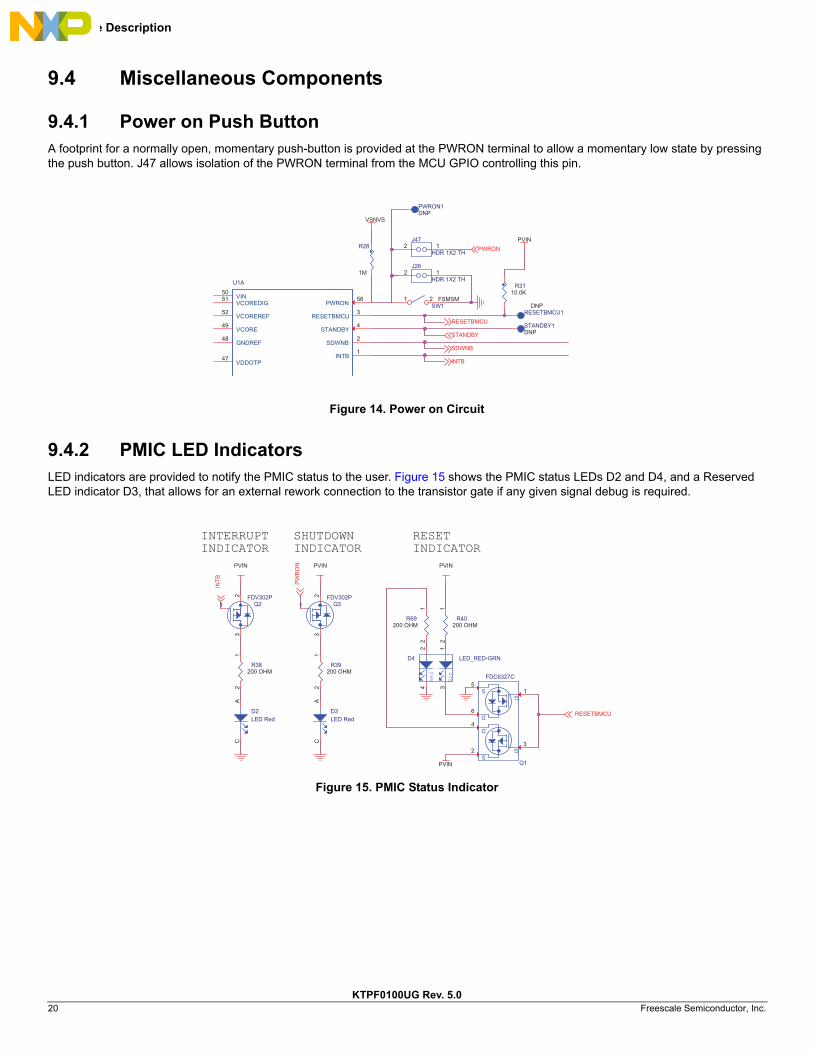
9.4 Miscellaneous Components
9.4.1 Power on Push ButtonA footprint for a normally open, momentary push-button is provided at the PWRON terminal to allow a momentary low state by pressing the push button. J47 allows isolation of the PWRON terminal from the MCU GPIO controlling this pin.
Figure 14. Power on Circuit
9.4.2 PMIC LED IndicatorsLED indicators are provided to notify the PMIC status to the user. Figure 15 shows the PMIC status LEDs D2 and D4, and a Reserved LED indicator D3, that allows for an external rework connection to the transistor gate if any given signal debug is required.
Figure 15. PMIC Status Indicator
PVIN
VSNVS
PWRON
STANDBY
INTB
RESETBMCU
SDWNB
U1A
INTB1
RESETBMCU3
SDWNB2
STANDBY4
VCOREDIG51
VCOREREF52
VDDOTP47
PWRON56
VCORE49
GNDREF48
VIN50
SW1FSMSM1 2
J47
HDR 1X2 TH12
PWRON1DNP
R3110.0K
J26
HDR 1X2 TH12
STANDBY1DNP
R28
1M
RESETBMCU1DNP
RESETINDICATOR
SHUTDOWNINDICATOR
INTERRUPTINDICATOR
PVIN PVIN PVIN
PVIN
RESETBMCU
INTB PW
RO
N
D2LED Red
AC
R38200 OHM
12
R39200 OHM
12
Q3FDV302P
1
32
D3LED Red
AC
R40200 OHM
12
Red
Grn
D4 LED_RED-GRN
42 1
3
Q2FDV302P
1
32
R69200 OHM
12
G
D
SG
S
D
Q1
FDC6327C
2
6
15
4
3
Hardware Description
KTPF0100UG Rev. 5.0Freescale Semiconductor, Inc. 21
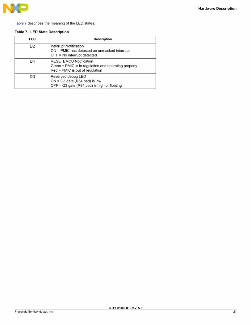
Table 7 describes the meaning of the LED states.
Table 7. LED State Description
LED Description
D2 Interrupt NotificationON = PMIC has detected an unmasked interruptOFF = No interrupt detected
D4 RESETBMCU NotificationGreen = PMIC is in regulation and operating properlyRed = PMIC is out of regulation
D3 Reserved debug LEDON = Q3 gate (R84 pad) is lowOFF = Q3 gate (R84 pad) is high or floating

Hardware Description
KTPF0100UG Rev. 5.022 Freescale Semiconductor, Inc.
9.4.3 Control/Programming InterfaceThis onboard USB-to-I2C interface comprises three basic blocks.
1. Controlling MCU (MC9S08JM60CGTE) for USB-I2C translation.2. 3.3 V LDO supply for external device controlling.
3. 8.25 V boost converter for OTP programming.
The control/programming interface allows one to program the onboard PF0100 PMIC. Alternatively, the interface can serve as a programmer for external devices though the connector J36.
Figure 16. Control/Programming Interface Schematic
Programming Interface
USB Connector Type A
BDM Programmer
ESD PROTECTION
Crystal
MAIN ICMC9S08JM60
LED INDICATORS
8V - Boost ConverterCLOSED
LDO REGULATOR 3.3V
VOUT = 1.242 X ( (R2/R1) + 1) = 3.3V
R2 = ((VOUT/1.242) -1) X R1
R1R2
Place on Bottom
Place on Bottom
Place on Bottom
Place on Bottom
Place on Bottom
D-D+G
VVUSBDN
USBDP
USB_PWRRST_JM60
MC
U_S
CL
MC
U_S
DA
ID1
ID0
EXTAL_JM60
XTAL_JM60
EXTAL_JM60XTAL_JM60
BKGD_JM60
BSTENVUSBEN
3V3ENVPGMEN
LRONLGON
ID0ID1
USBDNUSBDP
VUSB33
VUSB33RST_JM60
BKGD_JM60
LGON LRON
PWRON
MCU_SCL
BSTEN
BSTDNBSTUP
VPGMEN
BSTUPBSTDN
VDDOTPIN
3V3
3V3EN
VIN_USB
GPIO1GPIO2
MCU_SDA
VUSBEN
VIN_USB
VDDOTPIN_SNS
VDDOTPIN_SNS
USB_PWR
USB_PWR
USB_PWR
USB_PWRUSB_PWR
0
0
0
PVIN
0
0
0
0
0
VDDOTPIN
3V3
PWRONGPIO2
MCU_SDAMCU_SCL
GPIO1
VIN_USB
3V3
VIN_USB
R730
U4MAX686
LX16
VCC12
ISET6
VDD5
SHDN7
DN3 UP2
POK11LCDON14
REF9
PG
ND
1
FB10
NC15
DACOUT8
POL4
GN
D13
R514.7K
L9HI1812V101R-10
12
Q10FDN360P
1
32
C6022PF
12
R7120K
R67470
12
J35
HDR 2X3
1 23 4
65
C640.47UF
C801.0UF
C57
0.1uF
R77100K
R481.5KDNP
C62
0.1uF
R6647K
+ C7115UF
D7
ESD
9L5.
0ST5
GA
C
R411M
12
Q9
BSS1381
23
L10
22UH1 2
R65
10K
R60470K
C6122PF
12
U2
MC9S08JM60CGTE
PTC41
IRQ/TPMCLK2
RESET3
PTF0/TPM1CH24
PTF1/TPM1CH35
PTF4/TPM2CH06
PTF5/TPM2CH17
PTE0/TxD19
PTE1/RxD110
PTE2/TPM1CH011
PTE3/TPM1CH112
PTE4/MISO113
PTE5/MOSI114
PTE6/SPSCK115
PTE7/SS116
VD
D17
VS
S18
USBDN19
USBDP20
VUSB3321
PTG0/KBIP022
PTG1/KBIP123
PTB0/MISO2/ADP026
PTB1/MOSI2/ADP127
PTB2/SPSCK2/ADP228
PTB3/SS2/ADP329
PTB4/KBIP4/ADP430
PTB5/KBIP5/ADP531
PTD0/ADP8/ACMP+32
PTD1/ADP9/ACMP-33
VD
DA
D/V
RE
FH34
VS
SA
D/V
RE
FL35
PTD2/KBIP2/ACMPO36
PTG2/KBIP638
PTG3/KBIP739
BKGD/MS40
PTG4/XTAL41
PTG5/EXTAL42
VS
SO
SC
43
PTC0/SCL44
PTC1/SDA45
PTC246
PTC3/TxD247
PTC5/RxD248 PTF6
8
PTA525 PTA024
PTD737
GN
D49
R7547K
VBUSD-D+IDG
USB-MiniBJ34
1234
S2
5
S1
S3S4
J39
HDR 1X3123
Y1
12 MHz
I/O11
GND44
I/O33
GND22
D11LED Red
AC
D9
MBR130LSFT1G
A C
C63
0.1uF
R491.5KDNP
D6
ESD
9L5.
0ST5
GA
C
C74
0.1uF
U5
MIC5205
IN1
GND2
ADJ4
EN3
OUT5
R76470K
R61120K
C792.2uFDNP
R6410K
R74
0
D8
ESD
9L5.
0ST5
G AC R72
12.0K
C65
0.1uF
+ C5910UF
F10.5A
12
R55
100 + C73
4.7uF
+ C664.7UF
J36
HDR 2X4
1 23 4
657 8
R59374K
C72
22PF
C78470PF
R42
331 2
R6310K
R504.7K
C760.1uF
Q8
BSS1381
23
Q6FDN360P
1
32
Q5FDN360P
1
3 2
C770.1uF
D5
ESD
9L5.
0ST5
G
AC
+ C812.2UF
C58
0.1uF
L11HI1812V101R-10
12
R78100K
R68470
12
R56
604K
C751UF
D10
LED
Gre
en
AC
R45
331 2
PROGRAMMING CONNECTOR

KITPF0100EPEVBE Board Layout
KTPF0100UG Rev. 5.0Freescale Semiconductor, Inc. 23
10 KITPF0100EPEVBE Board Layout
10.1 Assembly Layer Top
Figure 17. Assembly Top Layer
KITPF0100EPEVBE Board Layout
KTPF0100UG Rev. 5.024 Freescale Semiconductor, Inc.
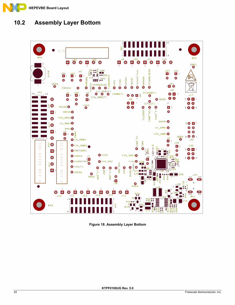
10.2 Assembly Layer Bottom
Figure 18. Assembly Layer Bottom

KITPF0100EPEVBE Board Layout
KTPF0100UG Rev. 5.0Freescale Semiconductor, Inc. 25
10.3 Top Layer Routing
Figure 19. Top Layer Routing

KITPF0100EPEVBE Board Layout
KTPF0100UG Rev. 5.026 Freescale Semiconductor, Inc.
10.4 Inner Layer 1 Routing
Figure 20. Inner Layer 1 Routing

KITPF0100EPEVBE Board Layout
KTPF0100UG Rev. 5.0Freescale Semiconductor, Inc. 27
10.5 Inner Layer 2 Routing
Figure 21. Inner Layer 2 Routing

KITPF0100EPEVBE Board Layout
KTPF0100UG Rev. 5.028 Freescale Semiconductor, Inc.
10.6 Bottom Layer Routing
Figure 22. Bottom Layer Routing

Bill of Materials
KTPF0100UG Rev. 5.0Freescale Semiconductor, Inc. 29
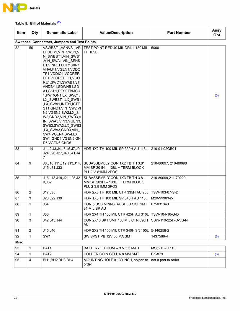
11 Bill of Materials
Table 8. Bill of Materials (2)
Item Qty Schematic Label Value/Description Part NumberAssy Opt
Freescale Components
1 1 U1 IC POWER MANAGEMENT CONSUMER/INDUSTRIAL QFN56
MMPF0100NPEP
2 1 U2 IC MCU 8BIT 48 MHZ 60 KB FLASH 2.7-5.5 V QFN48
MC9S08JM60CGTE
Active Components
3 1 U4 IC DAC CTRL BOOST INV +/-27.5 V -- 2.7-5.5 V QSOP16
MAX686EEE+
4 1 U5 IC LIN VREG LDO 1.5-15 V 150 MA 2.5-16 V SOT23-5
MIC5205YM5
5 1 U7 IC LIN VREG LDO 1.5-15 V 150 MA 2.5-16 V SOT23-5
MIC5205YM5(3)
6 1 Y1 XTAL 12 MHZ SER 9 PF SMT ECS-120-9-42X-CKM-TR
Diodes
7 1 D1 DIODE SCH PWR RECT 1 A 20 V SMT MBR120LSFT1G
8 3 D2,D3,D11 LED RED SGL 30 MA 0603 SML-LXFM0603SIC-TR
9 1 D4 LED DUAL GRN/RED 30 MA SMT LTST-C195KGJRKT
10 4 D5,D6,D7,D8 DIODE TVS ESD PROT ULT LOW CAP 5-5.4 V SOD-923
ESD9L5.0ST5G
11 1 D9 DIODE SCH PWR RECT 1 A 30 V SOD-123
MBR130LSFT1G
12 1 D10 LED GRN SGL 30 MA SMT 0603 SML-LXFM0603SUGCTR
Capacitors
13 7 C1,C3,C5,C8,C9,C12,C13
CAP CER 4.7 mF 10 V 10% X5R 0603 LMK107BJ475KA-T
14 12 C2,C4,C6,C7,C10,C11,C14,C19,C44,C45,C56,C77
CAP CER 0.1 mF 10 V 10% X5R 0402 C0402C104K8PAC
15 1 C15 CAP CER 0.01 mF 50 V 10% X7R 0402 GCM155R71H103KA55D
16 16 C16,C21,C22,C23,C24,C25,C26,C27,C28,C29,C30,C31,C32,C33,C82,C83
CAP CER 22 mF 10 V 20% X5R 0805 LMK212BJ226MG-T
17 1 C17 CAP CER 1000 pF 50 V X7R 5% 0402 0402X102J500SNT (3)
18 1 C18 CAP CER 10 mF 10 V 10% X7R 0805 GRM21BR71A106KE51L
19 5 C20,C34,C38,C42,C43 CAP CER 2.2 mF 6.3 V 20% X5R 0402 C0402C225M9PACTU
20 2 C35,C41 CAP CER 4.7 mF 6.3 V 20% X5R 0402 C0402X5R6R3-475MNP
21 3 C36,C37,C39 CAP CER 10 mF 16 V 10% X7R 0805 0805X106K160SNT
22 9 C40,C48,C49,C50,C51,C52,C54,C84,C87
CAP CER 1.0 mF 10 V 10% X5R 0402 CC0402KRX5R6BB105
23 2 C46,C53 CAP CER 0.22 mF 16 V 10% X7R 0402 GRM155R71C224KA12D
24 1 C47 CAP CER 0.47 mF 10 V 10% X7R 0402 GMC04X7R474K10NT-LF

Bill of Materials
KTPF0100UG Rev. 5.030 Freescale Semiconductor, Inc.
25 1 C55 CAP CER 1.0 mF 10 V 10% X5R 0402 CC0402KRX5R6BB105 (3)
26 5 C57,C58,C62,C63,C65 CAP CER 0.1 mF 16 V 10% X5R 0402 C1005X5R1C104K
27 1 C59 CAP TANT 10 mF 16 V 10% -- 3216-18 TAJA106K016R
28 3 C60,C61,C72 CAP CER 22 pF 25 V 5% C0G 0402 C0402C0G250-220JNE
29 1 C64 CAP CER 0.47 mF 16 V 10% X7R 0603 C0603C474K4RAC
30 1 C66 CAP TANT 4.7 mF 10 V 10% -- 3216-18 T491A475K010AT
31 1 C71 CAP TANT ESR 0.600 W 15 mF 25 V 10% -- 3528-21
TR3B156K025C0600
32 1 C73 CAP TANT 4.7 mF 25 V 10% -- 3528-21 TAJB475K025RNJ
33 1 C74 CAP CER 0.1 mF 25 V 10% X5R 0402 CC0402KRX5R8BB104
34 1 C75 CAP CER 1.0 mF 25 V 10% X5R 0603 C0603C105K3PAC
35 1 C76 CAP CER 0.1 mF 6.3 V 10% X7R 0402 C0402C104K9RACTU
36 1 C78 CAP CER 470 pF 50 V 5% COG 0603 06035A471JAT2A
37 1 C79 CAP CER 2.2 mF 16 V 10% X5R 0603 GRM188R61C225KE15D (3)
38 1 C80 CAP CER 1.0 mF 16 V 10% X5R 0603 C1608X5R1C105K
39 1 C81 CAP TANT ESR=1.800 W 2.2 mF 10 V 10% 3216-18
TPSA225K010R1800
40 1 C85 CAP CER 2.2 mF 6.3 V 20% X5R 0402 C0402C225M9PACTU (3)
41 1 C86 CAP CER 470 pF 50 V 5% COG 0603 06035A471JAT2A (3)
Inductors
42 1 L1 IND PWR 2.2 mH@100 kHZ 2.0 A 20% SMT
LPS3015-222ML_
43 1 L2 IND PWR 1 mH@100 kHz 6 A 20% SMT XAL4020-102MEC
44 4 L3,L4,L5,L8 IND PWR 1 mH@100 kHZ 2.4 A 30% SMT
LPS4012-102NLC
45 1 L6 IND PWR 1 mH@1 MHZ 2 A 30% SMT VLS252010T-1R0N
46 1 L7 IND PWR 1 mH@100 kHZ 2.65 A 20% SMT
LPS5015-102MLC
47 1 L9 IND FER 100 W@100 MHZ 8 A 25% SMD/1812
HI1812V101R-10
48 1 L10 IND PWR CHK 22 mH@1 kHZ 1 A 20% SMD
744773122
49 1 L11 IND FER 100 W@100 MHZ 8 A 25% SMD/1812
HI1812V101R-10
Resistors
50 6 R1,R3,R4,R6,R8,R16 RES -- 0.001 W 1/4 W 5% 0805 LMI-R001-5.0
51 1 R2 RES MF 1.0 W 1/16 W 1% 0402 RK73H1ETTP1R00F (3)
52 5 R7,R9,R10,R17,R70 RES -- 0.001 W 1/4 W 5% 0805 LMI-R001-5.0 (3)
53 1 R11 RES MF 0.001 W 1 W 1% 1206 CSNL1206FT1L00
54 5 R20,R23,R24,R27,R86 RES MF ZERO W 1/10 W 1% 0603 MC0603SAF0000T5E (3)
55 5 R21,R22,R25,R26,R85 RES MF ZERO W 1/10 W 1% 0603 MC0603SAF0000T5E
56 2 R28,R41 RES MF 1.0 MW 1/16 W 1% AEC-Q200 0402
CRCW04021M00FKED
Table 8. Bill of Materials (2)
Item Qty Schematic Label Value/Description Part NumberAssy Opt

Bill of Materials
KTPF0100UG Rev. 5.0Freescale Semiconductor, Inc. 31
57 2 R29,R79 RES MF 100 KW 1/16 W 5% 0402 RK73B1ETTP104J
58 3 R30,R31,R32 RES MF 10.0 KW 1/16 W 1% AEC-Q200 0402
CRCW040210K0FKED
59 3 R35,R73,R74 RES MF 0 W 1/10 W -- 0402 ERJ-2GE0R00X
60 4 R36,R37,R50,R51 RES MF 4.70 KW 1/16 W 1% 0402 RK73H1ETTP4701F
61 4 R38,R39,R40,R69 RES MF 200 W 1/10 W 1% 0402 ERJ2RKF2000X
62 2 R42,R45 RES MF 33.0 W 1/16 W 1% 0402 CR-02FL6---33R
63 2 R48,R49 RES MF 1.5 KW 1/16 W 5% 0402 CRCW04021K50JNED (3)
64 1 R55 RES MF 100 W 1/10 W 1% 0603 RK73H1JTTD1000F
65 1 R56 RES MF 604 KW 1/16 W 1% 0402 ERJ2RKF6043X
66 1 R59 RES MF 374 KW 1/16 W 1% 0402 RK73H1ETTP3743F
67 2 R60,R76 RES MF 470 KW 1/16 W 1% 0402 RK73H1ETTP4703F
68 1 R61 RES MF 120 KW 1/16 W 1% 0402 RK73H1ETTP1203F
69 3 R63,R64,R65 RES MF 10 KW 1/16 W 5% 0402 CRCW040210K0JNED
70 2 R66,R75 RES MF 47 KW 1/16 W 1% 0402 RK73H1ETTP4702F
71 2 R67,R68 RES MF 470 W 1/16 W 1% 0402 CR-02FL6--470R
72 1 R71 RES MF 20 KW 1/10 W 5% 0603 CR0603-JW-203ELF
73 1 R72 RES MF 12.0 KW 1/10 W 1% 0603 RK73H1JTTD1202F
74 2 R77,R78 RES MF 100 KW 1/16 W 1% 0402 RC0402FR-07100KL
75 1 R80 RES MF 27 KW 1/16 W 5% 0402 CRCW040227K0JNED (3)
76 1 R81 RES MF 470 KW 1/16 W 5% 0402 CR0402-16W-474JT (3)
77 2 R82,R83 RES MF 0 W 1/10 W -- 0402 ERJ-2GE0R00X (3)
Transistors
78 1 Q1 TRAN MOSFET DUAL N & P CHANNEL 2.5 V S-SOT6
FDC6327C
79 2 Q2,Q3 TRAN PMOS SW 120 MA 25 V SOT23 FDV302P
80 3 Q5,Q6,Q10 TRAN PMOS SW 2 A 30 V SSOT3 FDN360P
81 2 Q8,Q9 TRAN NMOS 50 V 220 MA SOT-23 BSS138
Table 8. Bill of Materials (2)
Item Qty Schematic Label Value/Description Part NumberAssy Opt
Bill of Materials
KTPF0100UG Rev. 5.032 Freescale Semiconductor, Inc.
Switches, Connectors, Jumpers and Test Points
82 56 VSWBST1,VSNVS1,VREFDDR1,VIN_SWC1,VIN_SWBST1,VIN_SWB1,VIN_SWA1,VIN_SENSE1,VINREFDDR1,VIN1,VHALF1,VGEN1,VDDOTP1,VDDIO1,VCOREREF1,VCOREDIG1,VCORE1,SWC1,SWAB1,STANDBY1,SDWNB1,SDA1,SCL1,RESETBMCU1,PWRON1,LX_SWC1,LX_SWBST1,LX_SWB1,LX_SWA1,INTB1,ICTEST1,GND1,VIN_SW2,VIN2,VGEN2,SW2,LX_SW2,GND2,VIN_SWB3,VIN_SWA3,VIN3,VGEN3,SWB3,SWA3,LX_SWB3,LX_SWA3,GND3,VIN_SW4,VGEN4,SW4,LX_SW4,GND4,VGEN5,GND5,VGEN6,GND6
TEST POINT RED 40 MIL DRILL 180 MIL TH 109L
5000
(3)
83 14 J1,J2,J3,J4,J5,J6,J7,J9,J24,J26,J27,J40,J41,J47
HDR 1X2 TH 100 MIL SP 339H AU 118L 210-91-02GB01
84 9 J8,J10,J11,J12,J13,J14,J15,J31,J33
SUBASSEMBLY CON 1X2 TB TH 3.81 MM SP 201H -- 138L + TERM BLOCK PLUG 3.81MM 2POS
210-80097, 210-80098
85 7 J16,J18,J19,J21,J25,J29,J32
SUBASSEMBLY CON 1X3 TB TH 3.81 MM SP 201H -- 138L + TERM BLOCK PLUG 3.81MM 3POS
210-80099,211-79220
86 2 J17,J35 HDR 2X3 TH 100 MIL CTR 335H AU 95L TSW-103-07-S-D
87 3 J20,J22,J39 HDR 1X3 TH 100 MIL SP 340H AU 118L M20-9990345
88 1 J34 CON 5 USB MINI-B RA SHLD SKT SMT 31 MIL SP AU
675031340
89 1 J36 HDR 2X4 TH 100 MIL CTR 425H AU 310L TSW-104-16-G-D
90 3 J42,J43,J44 CON 2X10 SKT SMT 100 MIL CTR 390H AU
SSW-110-22-F-D-VS-N
91 2 J45,J46 HDR 2X2 TH 100 MIL CTR 340H SN 105L 5-146258-2
92 1 SW1 SW SPST PB 12V 50 MA SMT 1437566-4 (3)
Misc
93 1 BAT1 BATTERY LITHIUM -- 3 V 5.5 MAH MS621F-FL11E
94 1 BAT2 HOLDER COIN CELL 6.8 MM SMT BK-879 (3)
95 4 BH1,BH2,BH3,BH4 MOUNTING HOLE 0.130 INCH, no part to order
not a part to order
Table 8. Bill of Materials (2)
Item Qty Schematic Label Value/Description Part NumberAssy Opt

Bill of Materials
KTPF0100UG Rev. 5.0Freescale Semiconductor, Inc. 33
96 1 F1 FUSE PLYSW 0.5 A 13.2 V SMT MICROSMD050F-2
Notes: 2. Freescale does not assume liability, endorse, or warrant components from external manufacturers that are referenced in circuit drawings or tables.
While Freescale offers component recommendations in this configuration, it is the customer’s responsibility to validate their application3. Do Not Populate
Table 8. Bill of Materials (2)
Item Qty Schematic Label Value/Description Part NumberAssy Opt
References
KTPF0100UG Rev. 5.034 Freescale Semiconductor, Inc.
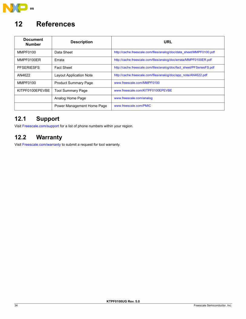
12 References
12.1 SupportVisit Freescale.com/support for a list of phone numbers within your region.
12.2 WarrantyVisit Freescale.com/warranty to submit a request for tool warranty.
Document Number
Description URL
MMPF0100 Data Sheet http://cache.freescale.com/files/analog/doc/data_sheet/MMPF0100.pdf
MMPF0100ER Errata http://cache.freescale.com/files/analog/doc/errata/MMPF0100ER.pdf
PFSERIESFS Fact Sheet http://cache.freescale.com/files/analog/doc/fact_sheet/PFSeriesFS.pdf
AN4622 Layout Application Note http://cache.freescale.com/files/analog/doc/app_note/AN4622.pdf
MMPF0100 Product Summary Page www.freescale.com/MMPF0100
KITPF0100EPEVBE Tool Summary Page www.freescale.com/KITPF0100EPEVBE
Analog Home Page www.freescale.com/analog
Power Management Home Page www.freescale.com/PMIC

Revision History
KTPF0100UG Rev. 5.0Freescale Semiconductor, Inc. 35
13 Revision History
Revision Date Description of Changes
1.0 11/2012 • Initial Release
2.0 2/2013 • Updated document for the latest GUI Revision 3.0.0.20• Added Figure 14 to section 8 Evaluation Board Schematic• Added TBB operation Mode.• Updated section 12.4 Using the Script Editor• Updated section 12.5 Loading a Configuration File
3.0 12/2013 • Added section 5 MMPF0100 Features• Added section 6 Hardware/Software Requirements
4.0 2/2015 • Removed references to older revision of EVB and GUI
5.0
8/2015 • Updated the Evaluation Board Schematic and related descriptions
8/2015 • Deleted section 6 KITPF0100EPEVBE Hardware/Software Deviation• Deleted Manufacturer column from Table 8

Information in this document is provided solely to enable system and software implementers to use Freescale products.
There are no express or implied copyright licenses granted hereunder to design or fabricate any integrated circuits based
on the information in this document.
Freescale reserves the right to make changes without further notice to any products herein. Freescale makes no
warranty, representation, or guarantee regarding the suitability of its products for any particular purpose, nor does
Freescale assume any liability arising out of the application or use of any product or circuit, and specifically disclaims any
and all liability, including without limitation consequential or incidental damages. “Typical” parameters that may be
provided in Freescale data sheets and/or specifications can and do vary in different applications, and actual performance
may vary over time. All operating parameters, including “typicals,” must be validated for each customer application by
customer’s technical experts. Freescale does not convey any license under its patent rights nor the rights of others.
Freescale sells products pursuant to standard terms and conditions of sale, which can be found at the following address:
freescale.com/SalesTermsandConditions.
How to Reach Us:
Home Page: freescale.com
Web Support: freescale.com/support
Freescale and the Freescale logo are trademarks of Freescale Semiconductor, Inc., Reg. U.S. Pat. & Tm. Off.
SMARTMOS is a trademark of Freescale Semiconductor, Inc. All other product or service names are the property of their
respective owners.
© 2015 Freescale Semiconductor, Inc.
Document Number: KTPF0100UGRev. 5.0
8/2015