kx 170a - maintenance manual honeywell
TRANSCRIPT

8/9/2019 KX 170A - Maintenance Manual Honeywell
http://slidepdf.com/reader/full/kx-170a-maintenance-manual-honeywell 1/586

8/9/2019 KX 170A - Maintenance Manual Honeywell
http://slidepdf.com/reader/full/kx-170a-maintenance-manual-honeywell 2/586

8/9/2019 KX 170A - Maintenance Manual Honeywell
http://slidepdf.com/reader/full/kx-170a-maintenance-manual-honeywell 3/586
%i RADIQMAINTENANCEANUAL EVISIONNSTRUCTIDNSNDHISTORY
MANUAL KX 170A/B-KX
175B/KY
195B
KPN 006-5053-06
REVISION 6 , December, 1977
Where R&R appears in the action column,
remove the page now in the maintenance manual and
replace it with the enclosed page; otherwise, ADD or DESTROY pages as listed. Retain these
instructions in the front of the maintenaqce manual as a Record of Revisions.
PAGE 1 ACTION I REASON FOR CHANGE
Cover
R&R
Updated transmitter and audio assembly and schematic to latest revision
Rev. Hist.
ADD
5-67A ADD
6-61
R&R
6-62
R&R

8/9/2019 KX 170A - Maintenance Manual Honeywell
http://slidepdf.com/reader/full/kx-170a-maintenance-manual-honeywell 4/586
% RADIOMAINTENANCEANUALREVISIONNSTRUCTIONSND HISTORY
MANUAL KX liOA/175
- KX 171x1/1758 -
KY
195/195B
REVISION
5, JUIY, 1976
Where R&Ii appears III the action column,
remove the page now in the mamterlarlce manual and
replace It with the enclrlsed page; otherwise,
ADD or DESTROY pages as llstetl. I~eta~n thesr
mstructions
in
the t’t.orlt of the maintenance manual as a Record of Revisions.
PAGE
Front
KX 1758
-05
& 1958
-04
ACTION
R&R
ADD
REASON FOR CHANGE
Revision No. changed
Add behind Green Tab
(KX 17OBE/175EIf - KY 195BE)

8/9/2019 KX 170A - Maintenance Manual Honeywell
http://slidepdf.com/reader/full/kx-170a-maintenance-manual-honeywell 5/586
%i RADIOMAINTENANCEANUAL EVISIONNSTRUCTIONSNDHISTORY
MIUAL KX 17OA/B - KX 175/B
- KY 195/B
REVISION
Where R&R appears in the action column, remove the page now in the maintenance manual and
replace it with the enclosed page;
otherwise, ADD or DESTROY pages as listed. Retain these
instructions in the front of the maintenance manual as a Record of Revisions.
Mod. to Eliminate Lock Up
Mod. to Narrow Bandpass Selectivity
Mod. to Eliminate VOR Error
Mod. to Eliminate VHF Comm Noise Squelch
Disc Capacitor Reliability
Transistor 007-0046-00 Substitution Information
Improved Faceplate Assembly
Discontinuance of Transistor KPN 007-0184-01
Place Behind Green Tab (KX
170A/KX 175)
Installation
Remove Tabs
and Text of First 3 Sections and Replace with
New Install.
Place Behind Blue Tab
Place Behind Front Page
Change in Para. 5.2.1(k)
Flow Chart Updated
Schematic Updated
B/M and Drawing Updated
B/M and Drawing Updated
Installation
Remove Tabs and
Text
of First 3 Sections and Replace with New Install.
Remove lable
of Contents.
Place Behind
Blue Tab
Drawing Updated
(KX 170B/KX 1758)
Installation
New Revision
Contents Revised
Change in Para. 5.2.1(j)
Change in Para. 5.2.5.8(s )
K-I 674

8/9/2019 KX 170A - Maintenance Manual Honeywell
http://slidepdf.com/reader/full/kx-170a-maintenance-manual-honeywell 6/586
PAGE
25
63A
65
67A
69
::
1 thru 6-28
31 thru 6-38
41 thru 6-50
57 thru 6-67
WION
&R
DD
DD
Ii:
DD
DD
&R
&R
&R
&R
REASON FOR CHAMGE
Flow Chart Revised
Schematic and Drawing Revised
thematic and Drawing Revised
thematic and Drawing Revised
thematic and Drawing Revised
thematic Revised
thematic Revised
/M and Drawings. Updated
/M and Drawings Updated
/M and Drawings Updated
/M and Drawings Updated
I
K- I h

8/9/2019 KX 170A - Maintenance Manual Honeywell
http://slidepdf.com/reader/full/kx-170a-maintenance-manual-honeywell 7/586
G RADIO AlNTfNANCEANUAL EVISIONNSTRUCTIONSNDHISTORV
MANUAL
Kx 170 A/B - KX 175/B - KY 195/B
REVISION August 1973
Where R&R appears in the action column,
remove the page now in the maintenance manual and
replace it with the enclosed page; otherwise, ADD or DESTROY pages as listed.
Retain these
instructions in the front of the maintenance manual as a Record of Revisions.
PAGF
1 ACTIIIY i
RFASflY ,FflR l?HAUCP
..-_
Front
..-. .-..
..-..-w..
. . . .
“..“l.W..
R&R Revision No. Change
KX 170BE
Destroy Replaced with new tab at rear of manual
Tab
KX 170BE
Destroy ‘Replaced by updated information
Page
Kx 170BE
New Tab covering all “BE” Units
KX 175BE
Add (Place tab at rear of Manual)
KY 195BE
Tab
3
KX 170BE
Add
Page
I
Revised Data]
KX 175BE
Add
Page
KY 195BE
Add
Page
New Data
New Data
A.dd Pages behind KX 170BE/ KX 175BE/
KY 195BE Tab

8/9/2019 KX 170A - Maintenance Manual Honeywell
http://slidepdf.com/reader/full/kx-170a-maintenance-manual-honeywell 8/586
KING RADIO MAINTENANCE MANUAL REVISION INSTRUCTIONS AND HISTORY
MANUAL KX 170A/KX 175/KY 195
REVISION LEVEL: 2, December, 1972
WhereR&R appears in the action column,
remove the page now in the maintenance manual and
replace it with the enclosed page; otherwise, ADD or DESTROY pages as listed.
Retain these
instructions in the front of the maintenance manual as a Record of Revisions.
PAGE
ACTION
REASON FOR CHANGE
THIS MANUAL IS A COMPLETE REPRINT. DESTROY OLD
MANUAL. THE NEXT 2 PAGES INDICATE WHAT CHANGES
HAVE BEEN MADE IN THE KX 170A/KX 1751KY 195 MANUAL
(REVISION 2).
Page 1 of 3

8/9/2019 KX 170A - Maintenance Manual Honeywell
http://slidepdf.com/reader/full/kx-170a-maintenance-manual-honeywell 9/586
KING RADIO MAINTENANCE MANUAL REVISION INSTRUCTIONS AND HISTORY
MANUAL Kx 170A/KX 1751KY 195
REVISION LEVEL: 2, December, 1972
Where R&R appears in the action column,remove the page now in the maintenance manual and
replace it with the enclosed page; otherwise,
ADD or DESTROY pages as listed. Retain these
instructions in the front of the maintenance manual as a Record of Revisions.
PA Gl?
----
I ACTTON 1
-_ - --_.
REASON FOR CHANGE
Front Page Add
(KX 170A/B-KX 175/B)(KY 195/B)
Front Page R&R
To correspond with new revision
Warranty
R&R
To correspond with new revision
Record of
Revision
Destroy
Manual Format Change
Service
Bulletin
Record
Destroy Manual Format Change
Manual Rev.
Instructions
& History Add
Manual Format Change
Service
Bulletin &
Memo
.Add
Manual Format Change
Vi R&R
Page numbers (Section VI) changed
l-2
R&R
Word “OPTIONAL” added
l-9
R&R
Word change
1-12 R&R
Deletion of information
2-13 Add Interconnect updated
2-13A
Add
Interconnect updated
2-i5 Add Interconnect updated
2-17 Add
Interconnect updated
4-19
R&R
Figure 4 - 12 changed
4-22
R&R
Figure 4-15 changed
4-23
R&R
Figure 4- 17 changed
4-26 R&R
Figure 4-21 changed
4-27 R&R
Figure 4-22 changed
5-1 R&R
Test equipment updated
5-2
R&R
Information deleted
5-3 R&R
Information change
5-4
R&R
Information deleted
5-5
R&R
Information change
5-37 R&R
Table 5-7 updated
5-40 R&R Table 5-8 updated
5-42 R&R
Table 5-9 updated
5-59
R&R
Schematic updated
5-91
R.R R
Table 5-13 updated
5-95
R&R
Paragraph 5. 7.4 updated
5-106
R&R
Paragraph d. updated
5-107
R&R
Table 5-14 updated
5-111 R&R
Paragraph 5.8.4 updated
5-113 R&R
Schematic updated
L
Page 2 of 3

8/9/2019 KX 170A - Maintenance Manual Honeywell
http://slidepdf.com/reader/full/kx-170a-maintenance-manual-honeywell 10/586
j-116
j-125
j-139
:hru
j- 149
Section VI
Tab
3-l
ru
10
15
RI
24
29
K-U
36
41
ru
75
ction V
rb
ction V
Photo updated
Schematic updated
Schematics updated
Contents updated
Parts list updated
PAGE
I
ACTION 1
REASON FOR CHANGE
j-116
R&R&R
j-125
R&R&R
j-139
:hru
j- 149
Adddd
Section VI
Tab
R&R&R
3-l
ru
10
R&R&R
15
RI
24 R&R&R
29
K-U
36
R&R&R
41
ru
75
ction V
rb
ction V
Parts list updated
Parts list updated
R&R&R
R&R&R
R&R&R
Adddd
Adddd
Parts list updated
Contents updated
Parts list updated, parts list revision record pages inserted,
remove and replace entire section.
Interconnect updated
Schematic updated
CUU
Idendumdendum
R&R&R
Adddd
Parts list & Assembly drawings updated
New (KX 170B/KX 175B/KY 195B) Maintenance Manual
Page 3 of 3

8/9/2019 KX 170A - Maintenance Manual Honeywell
http://slidepdf.com/reader/full/kx-170a-maintenance-manual-honeywell 11/586
KING,
KX 17OA/KX 75
NAVIGATIONECEIVE
COMMUNICATIONSRANSCEIV
INSTALLATIONANUA
006-0057-0
REV. 3 JANUARY, 1976
8/9/2019 KX 170A - Maintenance Manual Honeywell
http://slidepdf.com/reader/full/kx-170a-maintenance-manual-honeywell 12/586
KlNG
KX 170A/KX 175
NAVIGATION RECEIVER/COMMUNICATIONS TRANSCEIVER
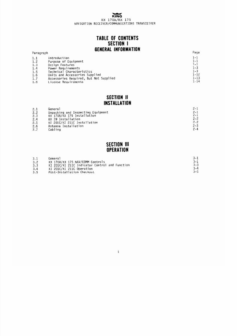
Paragraph
1.1
1.2
1.3
1.4
::6"
1.7
1.8
TABLEOF CONTENTS
SECTION
GENERALNFORMATION
Introduction
Purpose of Equipment
Design Features
Power Requirements
Technical Characteristics
Units and Accessories Supplied
Accessories Required, But Not Supplied
License Requirements
SECTIONI
INSTALLATION
2.1 General
2.2
Unpacking and Inspecting Equipment
2.3 KX 170A/KX 175 Installation
2.4 KX 39 Installation
2.5
KI 201C/KI 211C Installation
2.6 Antenna Installation
2.7 Cabling
SECTIONll
OPERATION
3.1
General
3.2
KX 170AjKX 175 NAV/COMM Controls
3.3
KI 201C/KI 211C Indicator Control and Function
3.4
KI
201C/KI 211C Operation
3.5
Post-Installation Checkout
Page
l-l
l-l
l-l
l-3
l-3
1-12
1-13
1-14
2-l
2-l
2-l
2-2
2-2
2-3
2-4
3-l
3-1
3-3
3-4
3-5
8/9/2019 KX 170A - Maintenance Manual Honeywell
http://slidepdf.com/reader/full/kx-170a-maintenance-manual-honeywell 13/586
KlNG
KX 17OAjKX 175
NAVIGATION RECEIVER/COMMUNICATIONS TRANSCEIVER
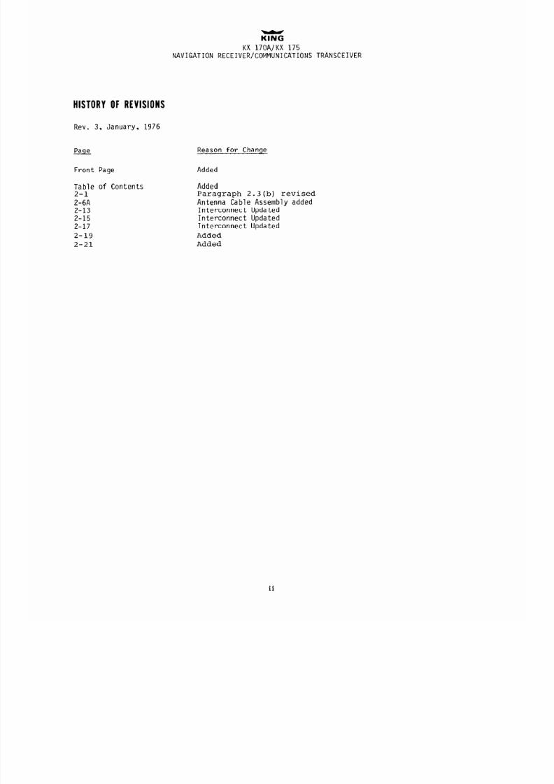
HISTORYOF REVISIONS
Rev. 3, January, 1976
Page
Front Page
Table of Contents Added
2-l
Paragraph 2.3(b) revised
2-6A
Antenna Cable Assembly added
2-13 Interconnect Updated
2-15 Interconnect Updated
2-17 Interconnect Updated
2-19
Added
2-21 Added
Reason for Change
Added
ii
8/9/2019 KX 170A - Maintenance Manual Honeywell
http://slidepdf.com/reader/full/kx-170a-maintenance-manual-honeywell 14/586
Kx mix 175
NAVIGATION RECEIVER /
COMMUNICATIONS TRANSCEIVER
SECTION
GENERALNFORMATION
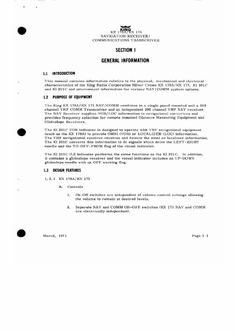
1.1 INTRODUCTION
This manual contains information relative to the physical, mechanical and electrical
characteristics of the King Radio Corporation Silver Crown Kx 170A/KX 175, KI 201C
and KI 211C and interconnect information for various NAV/ COMM system options.
1.2 PURPOSEFEQUIPMENT
The King KX 170A/KX 175 NAV/COMM combines in a single panel mounted unit a 360
channel VHF COMM Transceiver and an independent 200 channel VHF NAV receiver.
The NAV Receiver supplies VOR/LOC information to navigational converters and
provides frequency selection for remote mounted Distance Measuring Equipment and
Glideslope Receivers.
The KI 201C VOR Indicator is designed to operate with VHF navigational equipment
(such as the KX 170A) to provide OMNI (VOR) or LOCALIZER (LOC) information.
The VHF navigational receiver receives and detects the omni or localizer information.
The KI 201C converts this information to dc signals which drive the LEFT-RIGHT
needle and the TO-OFF-FROM flag of the visual indicator.
The KI 211 C ILS Indicator performs the same functions as the KI 201C. In addition,
it contains a glideslope receiver and the visual indicator includes an UP-DOWN
glideslope needle with an OFF warning flag.
1.3 DESIGN EATURES
1. 3. 1 KX 170A/KX 175
A.
Controls
1.
On-Off switches are independent of volume control settings allowing
the volume-to remain at desired levels.
2.
Separate NAV and COMM ON-OFF switches (KX 175 NAV and COMM
are electrically independent).
March, 197 1
Page l-l

8/9/2019 KX 170A - Maintenance Manual Honeywell
http://slidepdf.com/reader/full/kx-170a-maintenance-manual-honeywell 15/586
KING
JCX 170A/KX 175
NAVIGATION RECEIVER /
COMMUNICATIONS TRANSCEIVER
3. Automatic squelch eliminates pilot responsibility for continuously
monitoring squelch adjustments.
Squelch threshold automatically
adjusts to open on readable signals.
Test position opens squelch to
test COMM receiver sensitivity and to listen to extremely weak signals.
4.
Ident-Voice switch filters station ident from receiver audio.
5.
Frequency selector mechanism features human engineered concentric
knobs, airline type drum readout,
and blue-white or red back lighting.
Glideslope and DME switching is provided.
B.
Electronics
1.
Varactor diode tuned filters eliminates use of mechanical tuning shafts
and mechanisms.
2.
Balanced mixers for superior intermodulation, cross modulation, and
L. 0. radiation performance provide true 1 + 1 operation.
3.
Transistorized transmitter provides 5 watts minimum output power
and long term reliability superior to tube designs.
4.
The digital frequency synthesizers utilize state of the art integrated
circuits to replace all but 6 crystals (Kx 170A) and 7 crystals (Kx 175),
providing improved mean time between failure.
5.
Crystal filter selectivity both NAV and COMM.
6.
Carrier to noise squelch with carrier squelch back up functionally
described above.
7.
Tight AGC (typically 0. 5db from 10~~ to 20,000~~) minimizes audio
level variations.
C.
Construction
1.
Modular construction for ease of maintenance.
2.
Rack mounted, removable from the front panel.
3.
Anti-theft locking mechanism.
(Optional)
Page l-2
Rev. 2, December, 1972

8/9/2019 KX 170A - Maintenance Manual Honeywell
http://slidepdf.com/reader/full/kx-170a-maintenance-manual-honeywell 16/586
Kx 17Ko’AN/GKx17 5
NAVIGATION RECEIVER/
COMMUNICATIONS TRANSCEIVER
4.
Provisions for identifying radios as COMM 1, NAV 1 and COMM 2,
NAV 2 in dual installations.
1. 3. 2 KI BOlC/KI 211C
A.
Solid state
B.
Wedge lighting (blue-white or red)
C.
Autopilot couple capability.
D.
Automatic switching from VOR to ILS mode.
E. Proven reliability of KI 201/211 series indicators.
G.
Internal glideslope (KI 211C)
1.4 POWER EQUIREMENTS
The Kx 170A/KX 175 requires 13. 75 volts for proper operation.
Aircraft having
electrical power plants producing 27. 5 volts require the installation of a voltage
converter.
The KA 39 Voltage Converter,
designed to separately-convert NAV
and COMM 27. 5 volts to 13. 75 volts, may be conveniently remote mounted in the
aircraft.
The KI 2OlC/211C may be operated from either a 27. 5 or 13. 75 volt aircraft supply
volt age.
1.5 TECHNICALHARACTERISTICS
KX 170A TRANSCEIVER
SPECIFICATION
GE
MOUNTING:
SIZE:
KYX 170A NAV/COMM
3HARACTERISTIC
I
RAL
Panel mounted, no shock mounting required
6. 312 X 2. 600 X 14. 15
inches w/connectors.
(16. 03
X
6. 60
X
35. 94 centimeters. )
March, 197 1
Page l-3
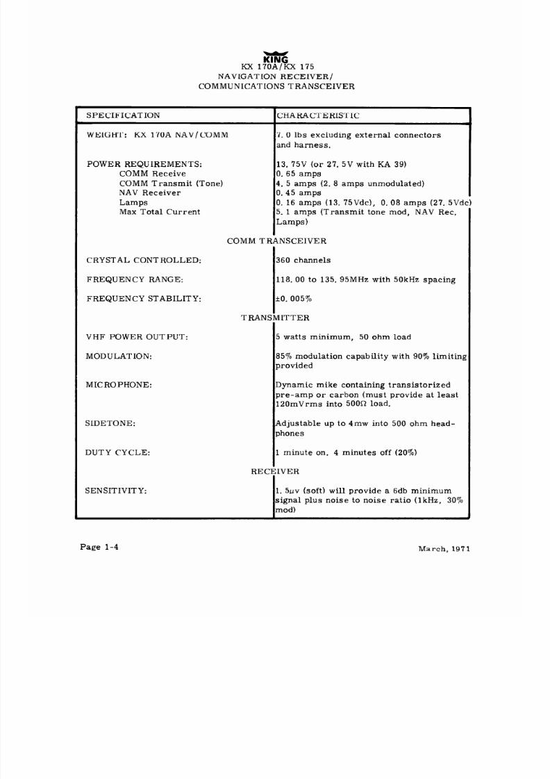
8/9/2019 KX 170A - Maintenance Manual Honeywell
http://slidepdf.com/reader/full/kx-170a-maintenance-manual-honeywell 17/586
Kx 17Ko’AN/GKx175
NAVIGATION RECEIVER /
COMMUNICATIONS TRANSCEIVER
S PE CIFI CAT ION I CHARACTERISTIC
WEIGHT: KX 170A NAV/ COMM
7. 0 lbs excluding external connectors
and harness.
POWER REQUIREMENTS:
COMM
Receive
COMM
Transmit (Tone)
NAV Receiver
Lamps
Max Total Current
13. 75V (or 27. 5V with KA 39)
0. 65 amps
4. 5 amps (2.
8 amps unmodulated)
0.45 amps
0. 16 amps (13.
75Vdc), 0. 08 amps
(27. 5Vdc)
5. 1 amps (Transmit tone mod, NAV Rec.
Lamps)
CRYSTAL CONTROLLED:
360 channels
FREQUENCY RANGE:
FREQUENCY STABILITY:
118.00 to 135. 95MHz with 50kHz spacing
*o. 005%
VHF POWER OUTPUT:
MODULATION:
MICROPHONE:
SIDETONE:
DUTY CYCLE:
SENSITIVITY:
COMM TRANSCEIVER
TRANI
REC
lIITTER
5 watts minimum, 50 ohm load
850/Omodulation capability with 90% limiting
provided
Dynamic m ike containing transistorized
pre-amp or carbon (must provide at least
12OmVrms into 500R load.
Adjustable up to 4mw into 500 ohm head-
phones
1 minute on, 4 minutes off (2070)
IVER
1. 5pv (soft) will provide a 6db minimum
signal plus noise to noise ratio (1kHz. 3070
mod)
Page l-4
March, 197 1

8/9/2019 KX 170A - Maintenance Manual Honeywell
http://slidepdf.com/reader/full/kx-170a-maintenance-manual-honeywell 18/586
KX 17Ko’ANIGKx17 5
NAVIGATION RECEIVER/
COMMUNICATIONS TRANSCEIVER
SPECIFICATION
SELECTIVITY:
SPURIOUS RESPONSES:
SQUELCH:
CHARACTERISTIC
Typical 6db at fl5kHz, 65db at f50kHz
Down at least 60db
Automatic squelch (carrier to noise) with
manual disable and carrier squelch overric
AGC CHARACTERISTICS:
i
le.
‘trom 10~~ to 20,000~~ audio output will no
vary more than 3db.
NAV RECEIVER
CRYSTAL CONTROLLED:
FREQUENCY RANGE:
SENSITIVITY:
Navigation
200 channels.
108. 00 to 117. 95MHz with 50kHz spacing.
1. 5pv (soft) will provide a half-flag indicat
1. Opv (soft) will provide a 6db signal + nois
noise
ratio.
ion
6
SELECTIVITY:
Typical 6db at fl9kHz
50db at f50kHz
SPURIOUS RESPONSES:
IDENT FILTER:
AGC CHARACTERISTICS:
Down at least 60db
Tone rejection, 15db, minimum
From 10~~ to 20,000~~ audio output will
not vary more than 3db.
NAV RECEIVER ACCURACY:
NAV OUT PUT :
Two sigma limit, *l. 5”
With LOC adjusted for 0. 35Vrms, VOR
=
0. 5Vrms (typical) into 20KR or greater
load impedance.
Rev. 1 January, 1972
Page l-5

8/9/2019 KX 170A - Maintenance Manual Honeywell
http://slidepdf.com/reader/full/kx-170a-maintenance-manual-honeywell 19/586
KlNG
KX 170A/KX 175
NAVIGATION RECEIVER/
COMMUNICATIONS TRANSCEIVER
~~
SPECIFICATION
1--
HARACTERISTIC
DME CHANNELING:
MO Ml M2 M3
108 - - 0 -
109 -
- - 0
110 0 - - -
111 0 0 - -
112 0 0 0 -
113 - 0 0 0
114 0 - 0 0
115 - 0 - 0
116 0
- 0 -
117 0
0 - 0
NOTE: (-) = OPEN, (0) =
ILS ENERGIZE:
GLIDESLOPE CHANNELING:
GS GS GS GS
108 109 110 111
108 0
- - -
109 -
0 - -
110 -
-
0 -
111 -
- - 0
112 -
- - -
113 -
- - -
114 -
- - -
115 -
- - -
116 -
- - -
117 - - - -
Kg Kl
.0x 0 0
.1x 0 0
.2x 0 0
.3x - 0
.4x - -
.5x 0 -
.6X - 0
.7x - -
.8X - -
.9x 0 -
DME COMMON.
K2 K3
50kHz
- -
. x0
0 -
.
x5
0
0 0
0 0
0 0
- 0
- -
0 -
- 0
- -
The ILS energize wire is connected to the
ILS common wire when the MHz selector
is in either the 108, 109, 110, or 111
position AND SIMULTANEOUSLY the kHz
selector is in either the 0. 10, 0. 15, 0. 30,
0. 35, 0. 50,
0. 55, 0. 70,
0. 75,
0.
90,or
0.
9:
pos it ion.
GS GS GS GS GS
GS
0. 1
0. 3 0. 5 0. 7 0. 9
50kHz
.0x -
- - - -
.x0 -
.1x 1
- - - -
.x5
0
.2x -
- - - -
.3x -
1 - - -
.4x -
- - - -
.5x - 1 - -
.6X -
- - - -
.7x -
- -
1 -
.8X -
- - - -
.9x -
- - - 1
5-
NOTE: (0) = ILS common, (-1 = open, (1) = either KN 70 A+ (KN 70 Installations)
or KX l’IOA/KX 175 A+ with 1KR source resistance (KI
SllC/KI 212
1
Page i-6
March, 197 1

8/9/2019 KX 170A - Maintenance Manual Honeywell
http://slidepdf.com/reader/full/kx-170a-maintenance-manual-honeywell 20/586
KING
KX 170A/KX 175
NAVIGATION RECEIVER/
COMMUNICATIONS TRANSCEIVER
SPECIFICATION
ICHARACTERISTIC
AI
AUXILARY AUDIO INPUTS:
FREQUENCY RESPONSES:
HEADPHONE OUTPUT:
SPEAKER OUTPUT:
l-CC 175 TF
TSO COMPLIANCE:
COMM Transmit
COMM Receive
VOR
LOC
Environmental
MOUNTING:
SIZE:
WEIGHT:
POWER REQUIREMENTS:
COMM Receive
COMM Transmit (Tone)
NAV Receive
Lamps
Max. total current
110
Three (3) 500 ohms with 30db isolation be-
tween any two.
Within 6db from 350Hz to 2500Hz.
50mw into 500 ohm
4. 5Vrms into auxilary input produces 5
watts audio output.
LNSCEIVER
C37b (DO-110, Class II)
C38b (DO-109)
C40a (DO- 114)
C36c (DO-131, Class C)
DAPBAAXXXXXX
Panel mounted, no shock mounting require1
6. 312 X 2. 600 X 14. 15 inches w/connectors
(16. 03 X 6. 60 X 35. 94 centimeters)
7. 0 lbs excluding external connectors and
harness.
13. 75V (or 27. 5V with KA 39)
0. 65 amps
4. 5 amps (2.8 amps unmodulated)
0.45 amps
0. 16 amps (13. 75Vdc), 0. 08 amps (27. 5Vdc)
5. 1 amps (Transmit tone mod, NAV Ret,
Lamps)
March, 197 I
Page l-7

8/9/2019 KX 170A - Maintenance Manual Honeywell
http://slidepdf.com/reader/full/kx-170a-maintenance-manual-honeywell 21/586
KING
KX 170A/KX 175
NAVIGATION RE CEIVER /
COMMUNICATIONS TRANSCEIVER
I
COMM TRANSCEIVER
CRYSTAL CONTROLLED:
FREQUENCY RANGE:
FREQUENCY STABILITY:
360 channels
118.00 to 135. 95MHz with 50kHz spacing
io. 005%
TRANSMITTER
VHF POWER OUTPUT:
MODULATION:
5 watts m inimum, 50 ohm load
85% modulation capability with 90% limiting,
less than 15% distortion at 80% mod.
MICROPHONE:
SIDETONE:
Carbon or dynamic mike containing trans-
istorized pre-amp (must provide at least
120mV,ms into 5000 load).
Adjustable up to 4mw into 500 ohm head-
phones
DUTY CYCLE: 1 minute on, 4 minutes off (20%)
RECEIVER
SENSITIVITY:
SELECTIVITY:
SPURIOUS RESFONSES:
SQUELCH:
AGC CHARACTERISTICS:
1. 5pv (soft) will provide a 6db minimum
signal plus noise to noise ratio
Typical 6db at fl5kHz, 65db at f50kHz
Down at least 60db
Automatic squelch (carrier to noise) with
manual disable and carrier squelch overridt
From 10~~ to 20,000~~ audio output will
not vary more than 3db.
NAV RECEIVER
CRYSTAL CONTROLLED:
200 channels.
Page l-8
Rev. 1 January, 1972

8/9/2019 KX 170A - Maintenance Manual Honeywell
http://slidepdf.com/reader/full/kx-170a-maintenance-manual-honeywell 22/586
KING
KX 170A/KX 175
NAVIGATION RE CE IVER /
COMMUNICATIONS TRANSCEIVER
SPECIFICATION
FREQUENCY RANGE:
SENSITIVITY:
Navigation
SELECTIVITY:
SPURIOUS RESPONSES:
IDENT FILTER:
AGC CHARACTERISTICS:
ACCURACY:
NAV OUTPUT:
DME CHANNELING:
CHARACTERISTIC
108. 00 to 117. 95MHz with 50kHz spacing.
1. 5/*v (soft) will provide a half-flag indicati
1. Okv (soft) will provide a 6db signal + noise
n
noise
Typical 6db at *lSkHz
75db at f50kHz
Down at least 60db
Tone rejection, 15db, minimum
From 10~~ to 20,000~~ audio output will
not vary more than 3db
Two sigma limit, fl. 0”
With LOC adjusted for 0. 35Vrms, VOR
= 0. 5Vrms (typical) into 20KR or greater
load impedance.
MO Ml
Kg
108 - -
:1 K2 K3
.0x0 --
109
- - - 0
110
0 - - -
111
0 0 - -
112
0 0 0 -
113
- 0 0 0
114
0 - 0 0
115
- 0 - 0
116
0 - 0 -
117
0 0 - 0
.1x
0
0
0
-
.2x
0
0
0
0
.3x
-
0
0
cl
.4x
-
-
0
0
.5x
0
-
-
0
.6X
-
0
-
-
.7x
-
-
0
-
.8X
-
-
-
0
.9x
0
-
-
-
NOTE: (-) = OPEN, (0) = DME COMMON.
I
50kHz
. x0
1
.x5
0
Rev. 2, December, 1972
Page l-9

8/9/2019 KX 170A - Maintenance Manual Honeywell
http://slidepdf.com/reader/full/kx-170a-maintenance-manual-honeywell 23/586
KlNG
KX 170A/KX 175
NAVIGATION RECEIVER/
COMMUNICATIONS TRANSCEIVER
SPECIFICATION
CHARACTERISTIC
ILS ENERGIZE:
The ILS energize wire is connected to the
ILS common wire when the MHz selector
is in either the 108, 109, 110, or 111
position AND SIMULTANEOUSLY the kHz
selector
is
in either the 0.10, 0. 15, 0. 30,
0. 35, 0. 50, 0. 55, 0. 70, 0. 75, 0. 90 or 0. 95
pos it ion,
GLIDESLOPE CHANNELING:
GS GS GS GS
GS GS GS GS GS GS
108 109 110 111
0, 1 0. 3 0. 5 0. 7 0. 9
50kHz
108 0 - - -
-ox - - - - -
.x0 -
109 - 0 - -
.1X 1 - - - -
.x5 0
110 - - 0 -
.2x - - - - -
111 - - - 0
.3x - 1 - - -
112 - - - -
.4X - - - - -
113 - - - -
.5x - - 1 - -
114 - - - -
.6X _ _ _ - _
115 - - - -
.7x - - - 1 -
116 - - - -
.8X _ _ _ _ _
117 - - - -
.9x - - - - 1
NOTE: (0) = ILS common, (-) = open,
(1) = either KN 70 A+ (KN 70 Installations
or KX 170A, KX 175 A+ with 1KR source resistance (KI ZllC/KI 212
installations).
I
AUDIO
A.UXILARY AUDIO INPUTS:
Three (3) 500 ohms with 30db isolation be-
tween any two.
FREQUENCY RESPONSES:
HEADPHONE OUTPUT:
SPEAKER OUTPUT:
Within 6db from 350Hz to 2500Hz.
50mw into 500 ohm
4. 5Vrms into auxilary input produces 5
watts audio output
Page l-10
March, 197 1

8/9/2019 KX 170A - Maintenance Manual Honeywell
http://slidepdf.com/reader/full/kx-170a-maintenance-manual-honeywell 24/586
KING
KX 17OA/KX 175
L
NAVIGATION RE CEIVER /
COMMUNICATIONS TRANSCEIVER
KI BOlC/KI 211C INDICATOR
SPECIFICATION
GE
SIZE:
KI 201C VOR Indicator:
KI 211C ILS Indicator:
WEIGHT:
KI 201C VOR Indicator:
KI 2 11 C ILS Indicator:
POWER REQUIREMENTS:
KI 201C VOR Indicator:
KI 211 C ILS Indicator:
VOI
LOCALIZER CENTERING:
LOCALIZER SENSITIVITY:
OMNI ACCURACY:
OMNI SENSITIVITY:
INPUT LEVELS:
GLID
SENSITIVITY:
CHARACTERISTIC
<RAL
3. 25 X 3. 25 X 8. 3
inches
(8. 255 X 8. 255 X 21. 082 centimeters)
3. 25 X 3. 25 X 8. 3 inches
(8. 255 X 8. 255 X 21. 082 centimeters)
2. 5
lbs,
3. 0 lbs.
lOOma (day)
lOOma (day)
2 20ma (night)
160ma (night)
200ma (day)
200ma (day)
320ma (night)
260ma (night)
r LOC
Within +100/o of standard deflection (+ l/2
needle width)
4db tone ratio will give 4 dot scale deflection
f two needle widths
10” of course width gives full scale deflection
LOC .35Vrms
SLOPE
2Opv (soft) for half flag and 60% of standard
deflection (1 dot)
March, 197 1
Page l-11

8/9/2019 KX 170A - Maintenance Manual Honeywell
http://slidepdf.com/reader/full/kx-170a-maintenance-manual-honeywell 25/586
KlNG
KX 170A/KX 175
NAVIGATION RECEIVER/
COMMUNICATIONS TRANSCEIVER
SPECIFICATION
CENTERING:
CHARACTERISTIC
Within 10% of standard deflection (200~~ to
30,000~~) (*l needles width)
SPURIOUS RESPONSES:
SELECTIVITY:
At least 40db down.
150kHz minimum 6db bandwidth
6OOkHz maximum 40db bandwidth
EXTERNAL LOAD:
Will operate an external autopilot load.
KA 39 VOLTAGE CONVERTER
SIZE: 3. 500 X 2.000 X 5. 500 inches
(8. 889 X 5. 18 X 13. 87 centimeters)
WEIGHT: 1. 1 lbs. excluding harness
POWER:
A
B
Input Volts
27. 5vdc
27. 5vdc
output Volts 13. 75vdc 13. 75vdc
(nominal) (nominal)
Input Current continuous
Input Current 40% duty
------__
Output Current continuous 1. 5A 0. 75A
Output Current 40% duty 5. OA
-------_
1.6
A.
King KX 170A NAV/COMM (069-1017-00)
B.
King Kx 175 NAV/COMM (069-1016-00)
C.
King KX 170A/KX 175 Installation Kit (050-1142-00) includes:
03V-0061-00
Connector, Antenna (TED 9-10-Z)
030-1019-00
Clamp, Cable Hall
030-2101-04 Connector, 42 pin (Amphenol
26-l
90-42)
047 - 1743 -0 1 Plate, Connector Mounting
047-1851-00
Cover, Connector Mounting Plate
057-1214-00 Decal, COMM 1
Page 1-12
Rev. 2, December, 1972
8/9/2019 KX 170A - Maintenance Manual Honeywell
http://slidepdf.com/reader/full/kx-170a-maintenance-manual-honeywell 26/586
KING
KX 17OA/KX 175
NAVIGATION RECEIVER/
COMMUNICATIONS TRANSCEIVER
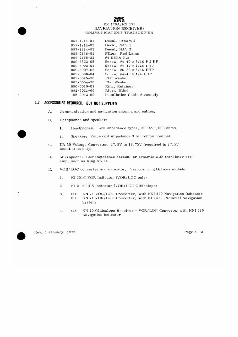
057-1214-01
Decal, COMM 2
057-1214-02
Decal, NAV 1
057-1214-03 Decal, NAV 2
088-0136-01
Filter, Red Lamp
089-2188-22 #4 ESNA Nut
089-5523-05
Screw, #4-40X 5/16 Fil HP
089-5903-05 Screw, #4-40 X 5/16 PHP
089-5907-05 Screw, #6-32 X 5/16 PHP
089-6008-04
Screw, #4-40 X l/4 FHP
089-8025-30 Flat Washer
089-8094-30
Flat Washer
090-0019-07
Ring, Retainer
092-5021-00
Rivet, Blind
155-2013-00
Installation Cable Assembly
1.7 ACCESSORIESEQUIRED, UTNOTSUPPLIED
A.
Communication and navigation antenna and cables.
B.
Headphones and speaker:
1.
Headphones :
Low impedance types, 300 to 1,000 ohms.
2.
Speaker: Voice coil impedance 3 to 6 ohms nominal.
C. KA 39 Voltage Converter,
27. 5V to 13. 75V
(required in 27. 5V
installation only).
D.
Microphone: Low impedance carbon,
or dynamic with-transistor pre-
amp, such as King KA 14.
E.
VOR/LOC converter and indicator.
Various King Options include:
1.
KI 201 C VOR Indicator (VOR/ LOC only)
2.
KI 211C ILS Indicator (VOR/ LOC Glideslope)
3. (a)
KN 71 VOR/LOC Converter,
with KNI 520 Navigation Indicator
b)
KN 71 VOR/LOC Converter,
with KPI 550 Pictorial Navigation
System
4. (a)
KN 70 Glideslope Receiver -
VOR/LOC Converter with KNI 520
Navigation Indicator
Rev. 1 January, 1972
Page 1-13
8/9/2019 KX 170A - Maintenance Manual Honeywell
http://slidepdf.com/reader/full/kx-170a-maintenance-manual-honeywell 27/586
Kx lfiiE$iX 175
NAVIGATION RECEIVER/
COMMUNICATIONS TRANSCEIVER
lb)
KN 70 Glideslope Receiver - VOR/LOC Converter with KPI 550
Pictorial Navigation System
5. (4
KN 74 Area Navigation Computer with KI 212 CD1 and Glideslope
Receiver.
b)
KN 74 Area Navigation Computer with KN 70 Glideslope Receiver
VOR/LOC Converter and KPI 550A Pictorial Navigation System.
1.8 LICENSE EQUIREMENTS
The Federal Communications Commission requires that the operator of the transmitter
in this equipment holds a Restricted Radio Telephone Operator Permit, or higher c lass
license.
A permit may be obtained by a U. S. citizen from the nearest field office of the
F-CC; no examination is required.
This equipment has been type accepted by the FCC and entered on their list of type
accepted equipments as King KX 17OA/ KX 175 and must be identified as King KX 170A
or King KX 175.
-CAUTION -
The VHF transmitter in this equipment is guar-
anteed to meet Federal Communications Comm -
ission approval only when King crystals are used.
Use of other than King crystals is considered an
unauthorized modification.
Page 1-14
Rev. 1 January, 1972
8/9/2019 KX 170A - Maintenance Manual Honeywell
http://slidepdf.com/reader/full/kx-170a-maintenance-manual-honeywell 28/586
KI
7
X 170A KX 175
NAVIGATION RECEIVER /
COMMUNICATIONS TRANSCEIVER
SECTIONI
INSTALLATION
2.1 GENERAL
This section contains suggestions and factors to consider before installing the KX 170A/
KX 175 NAV/COMM unit, KA 39 Voltage Converter (27. 5V installations only), and
KI 20 1C /KI 2llC Indicator. Close adherence to these suggestions will assure a more
satisfactory performance from the equipment.
2.2 UNPACKINGND NSPECTINGQUIPMENT
Exercise extreme care when unpacking each unit.
Make a visual inspection of each unit
for evidence of damage incurred during shipment.
If a claim for damage is to be made,
save the shipping container to substantiate the claim.
When all equipment is removed,
place in the shipping container all packing materials for use in unit storage or reship-
ment.
The KX 170A/KX 175 installation will conform to standards designated by the
customer,
installing agency and existing conditions as to unit location and type of install-
ation.
2.3 KX 17OA/KX 75 INSTALLATION
Listed below are factors and suggestions to consider before installing your KX 170A/
KX 175 system. Close adherence to these suggestions will assure more satisfactory
performance from your equipment.
(4
The KX 170A/KX 175 is mounted rigid in the aircraft panel. Mark and cut the
mounting hole as shown in Figure 2-7.
The purpose of the “behind aircraft panel
mount cutout is to allow a margin of error in cutout size and prevent the mount-
ing tray front edge from being visible. The mounting tray bottom lip should ex-
tend through the mounting hole flush with the instrument panel to insure proper
plug pin engagement.
(b)
(c)
Avoid mounting close to any high external heat source.
If this is done, no blower
or ram air cooling will be required. For blower or Ram Air cooling see
Figures 2-11 and 2-12.
Remember to allow adequate space for installation of cables and connectors.
(4
Secure the mounting rack to instrument panel per Figure 2-7. The rear mount-
ing bosses should be attached to the airframe by means of support brackets.
Rev.
3, January, 1976 Page 2-l

8/9/2019 KX 170A - Maintenance Manual Honeywell
http://slidepdf.com/reader/full/kx-170a-maintenance-manual-honeywell 29/586
(e)
(kit)
2.4
KA39 INSTALLATION
(a)
Select the KA 39 location considering good thermal conductivitv to the airframe,
convenient cable routing, proximity to the KX 17OA/KX 175 and separation from
other heat sources.
(b)
(c)
(4
2.5
(4
(b)
(c)
KI
Y
X 170A KX 175
NAVIGATION RECEIVER/
COMMUNICATIONS TRANSCEIVER
Slide the KX 17OA/KX 175 into the rack and secure by turning
locking screw on
the front panel.
-CAUTlON-
Do not force locking tab screw.
Each KX 170A/KX 175 installation kit contains a locking bar (KPN 047-1720-OO),
bracket (KPN 047-1721-00) and two rivets (KPN 092-5021-00).
These may be
installed at customer’s option to provide a means of locking the radio to the in-
strument panel with a padlock located on the lower rear corner of the mounting
tray.
Installation consists of riveting the bracket to the mounting tray as shown in
Figure 2 -7.
After the radio installation is complete, the locking bar may be
inserted and a small padlock affixed to deter theft.
The installing agency will supply and fabricate all external cables. The plugs
required are supplied by King Radio.
(For use in 27. 5 volt installations only)
Refer to Figure 2-6 for the KA 39 mounting dimensions.
Secure the KA 39 firmly in place.
The installing agency will supply and fabricate external cables.
Kl 2OlUKI 211C INSTALLATION
Carefully select the KI 2OlC/211C panel location for unobstructed vision, mini-
mum parallax and adequate clearance for the instrument case and installation
of cables and connectors.
Refer to Figure 2-5 for the KI 201C /211C mounting dimensions.
A standard 3 l/8” instrument hole is required.
Page 2-2
March, 197 1

8/9/2019 KX 170A - Maintenance Manual Honeywell
http://slidepdf.com/reader/full/kx-170a-maintenance-manual-honeywell 30/586
KING
KX 170A/KX 175
NAVIGATION RECEIVER/
COMMUNICATIONS TRANSCEIVER
(4
Secure the KI 2OlC /211C firmly in place.
(e)
The installing agency will supply and fabricate the external cable.
The plugs
required are supplied by King Radio.
Autopilot connection: The KI 20 1C /2 11C are capable of driving an autopilot load
of 1KR. The deflection sensitivity of the KI 211C Glideslope should be readjust-
ed.
Potentiometer R465, located in the KI 211C unit, is used to compensate for
the additional lKS2 load.
No adjustment is necessary if the autopilot is of the high
impedance type (over 10KQ.
No adjustment is necessary in the KI 201C or
KI 2 11C VOR/LOC with the addition of an autopilot load (1KQ because the com-
parator circuit has a very low output impedance.
With the addition of a 1KR load
the deflection sensitivity will change from 20”
course width to approximately 22”
An omni error adjust potentiometer,
R316, is accessible from the front of the
indicator by removing the OBS knob.
This is for final calibration of the omni
system after installing in aircraft.
The range of the error pot is approximately
f5”.
It should be noted that this potentiometer does not affect localizer center-
ing.
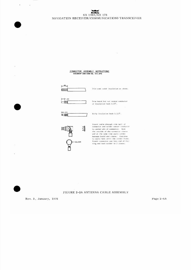
RG-188/U coaxial cable is recommended for the glideslope antenna interconnect.
Refer to Figure 2-3 for connector assembly.
2.6 ANTENNANSTALLATION
(4
Conventional 50 ohm horizontally polarized NAV and vertically polarized COMM
antennas are required with the KX 170A/KX 175.
Vertical bent whip antennas
are not recommended.
Wideband COMM antennas (KA 3 1 and KA’ 3 1A) provide
efficient operation over the COMM band.
Antennas should be installed per manu-
facturers recommendations.
Additional recommendations are as follow:
COMM ANTENNA
1.
Mount antenna on flat metal surface or install a ground plane at least
18 inches square.
2.
The antenna should be well removed from any projections and the
engine(s) and propeller.
3.
NAV and COMM Antennas must be well separated to minimize COMM’
interference to NAV while transmitting.
March, 197 1
Page 2-3

8/9/2019 KX 170A - Maintenance Manual Honeywell
http://slidepdf.com/reader/full/kx-170a-maintenance-manual-honeywell 31/586
KI
7
X 170A
KX 175
NAVIGATION RECEIVER/
COMMUNICATIONS TRANSCEIVER
NAVANTENNA
1.
The location should be well removed from other antenna, projections and
engine(s) .
It should have a clear line of sight area if possible.
2.
The antenna MUST BE mounted symmetrically with the centerline of the
aircraft.
3.
Avoid running other coaxial cables and wires with the NAV antenna cable.
(b)
The antenna connectors on the KX 170A/KX 175 unit are identified on the rear
die casting.
-NOTE-
With the KX 17OA/KX 175 viewed from the rear
the NAV antenna connector is on the right and
the COMM antenna connector is on the left. This
means that the NAV frequency selector and NAV
antenna are on opposite sides of the radio. The
COMM frequency selector and COMM antenna
connector are also on opposite sides of the radio.
-CAUTION -
Review the above information carefully. Inter-
changed antenna connections will cause erroneous
NAV operation and in some installations could in-
troduce 7 watts of transmitter power into a NAV
receiver causing damage to that unit.
(c)
Refer to Figure 2-4 for a dual omni antenna installation if two navigation receiv-
ers are used. VOR antenna duplexers normally cause a 3db signal loss.
(d)
Refer to Figure 2-2 for the COMM and NAV antenna cable connector assembly.
Solder tack the snap on shield to the connector base at two points to insure that
a good electrical ground is made.
2.7 CABLING
(4
The length and routing of the external cables must be carefully studied and plann-
ed prior to installation.
Avoid sharp bends and placing cables too near the air-
craft control cables.
Page 2-4
March, 197 1

8/9/2019 KX 170A - Maintenance Manual Honeywell
http://slidepdf.com/reader/full/kx-170a-maintenance-manual-honeywell 32/586
ZK
KX 170A/KX 175
NAVIGATION RECEIVER /
COMMUNICATIONS TRANSCEIVER
(b)
Fabricate the external cables in accordance with the installation drawing that
fulfills the system requirement.
-NOTE-
Use good quality stranded wire that will not
support a flame and with at least 600 volt
insulation. It is recommended that the mike
audio line be in a shielded-twisted pair.
(c)
Since other radio and navigation equipment will possibly utilize the same speaker
circuits for muting, speaker selection and microphone switching must be devised
by the installing agency. The KX 170A/KX 175 does not shunt the speaker line of
other equipment when the off-on-test switch is turned “off”.
PI71
KPN 030-2101-04
I
CONNECTOR VIEW’ED
FROM CABLE END
696-6002-00 (R-01
FIGURE 2- 1 KX-170A/KX 175 CONNECTOR PIN LOCATIONS
March, 197 1 Page 2-5

8/9/2019 KX 170A - Maintenance Manual Honeywell
http://slidepdf.com/reader/full/kx-170a-maintenance-manual-honeywell 33/586
Page 2-6
KI
7
X 170A KX 175
NAVIGATION RECEIVER/
COMMUNICATIONS TRANSCEIVER
/SOLDER
Trim coax cable outer insulation as shown.
Fold braid back over outer cover of coax.
Do not cross strands.
Solder center conductor to center pin of
conductor.
Make sure front end of braid
(Point of fold) is even with bottom of con-
nector. (Shown by arrows)
Slide connector cap,
with clearance hole in
position to clear dielectric, on to connector
until it snaps in place.
Push braid forward and flatten against con-
nector cap and solder.
Solder tat connector cap to connector in at
least two places to insure good electrical
contact.
696-6003-00
FIGURE 2-2 ANTENNA CABLE ASSEMBLY
March, 197 1
a
8/9/2019 KX 170A - Maintenance Manual Honeywell
http://slidepdf.com/reader/full/kx-170a-maintenance-manual-honeywell 34/586
KlNG
KX 170A/KX 175
NAVIGATION RECEIVER/COMMUNICATIONS TRANSCEIVER
CONNECTOR ASSEMBLY INSTRUCTIONS
DOCUMENT 006-105.8~00, OCT, 1972
7
Trim braid but not center conductor
or insulation back 0.25”.
Strip insulation back 0.125”.
SOLDER
Insert cable through side wall of
3l
connector and solder center conductor
to center pin of connector.
Heat
the outside of the connector sleeve
and at the same time apply solder
between braid and %leew.
Cant inue
to apply heat until the solder flows.
Insert connector cap into end of fit-
ting and tack solder in 2 places.
FIGURE 2-2A ANTENNA CABLE ASSEMBLY
Rev. 3,
January, 1976
Page 2-6A

8/9/2019 KX 170A - Maintenance Manual Honeywell
http://slidepdf.com/reader/full/kx-170a-maintenance-manual-honeywell 35/586
KING
.KX 170A/KX 175
NAVIGATION RECEIVER/
COMMUNICATIONS TRANSCEIVER
696-6004-00
FIGURE 2-3 GLIDESLOPE ANTENNA CABLE CONNECTOR ASSEMBLY
March, 197 1
Page 2-7

8/9/2019 KX 170A - Maintenance Manual Honeywell
http://slidepdf.com/reader/full/kx-170a-maintenance-manual-honeywell 36/586
Page 2-8
KING
KX 170A/KX 175
NAVIGATION RECEIVER/
COMMUNICATIONS TRANSCEIVER
696-6005-00
FIGURE 2-4 DUAL OMNI ANTENNA INSTALLATION
March, 197 1
a

8/9/2019 KX 170A - Maintenance Manual Honeywell
http://slidepdf.com/reader/full/kx-170a-maintenance-manual-honeywell 37/586
KI G
KX
7
70A KX 175
NAVIGATION RECEIVER /
COMMUNICATIONS TRANSCEIVER
FIGURE 2-5 KI 20 1C /KI 2 11C
INDICATOR OUTLINE AND MOUNTING DRAWING
March, 197 1
Page 2-9

8/9/2019 KX 170A - Maintenance Manual Honeywell
http://slidepdf.com/reader/full/kx-170a-maintenance-manual-honeywell 38/586
KING
KX 170A/KX 175
NAVIGATION RECEIVER /
COMMUNICATIONS TRANSCEIVER
.093R
2 PLCS.
USE% PAN. HO SCREWS
NOTES:
1. ALL 01~ENsl0Ns IN PARENTHESIS ARE INCENTIMETERS.
2.WEIGHT: I.1 Ibs
3 TERMINALS WILL TAKE 16 TO22AWG W IRE.
4.TERMlNALS ARE =5-40X1/4 60 HO SCREWS
I-
113.870~
OONOT MOUNT IN CLOSE PROXIMITY
TO HEATER DUCT OR OTHER SOURCES OF HEAT
155-5076-00 (R- )
I
WARNING
-
FIGURE
2-6 KA 39
VOLTAGE CONVERTER OUTLINE AND MOUNTING DRAWING
Page 2 - 10
March, 197
1

8/9/2019 KX 170A - Maintenance Manual Honeywell
http://slidepdf.com/reader/full/kx-170a-maintenance-manual-honeywell 39/586
KING
KX 170A/KX 175
NAVIGATION RECEIVER /
COMMUNICATIONS TRANSCEIVER
6. IO 0
115.50)
C UT OU T D IY EN S ON S F OR
B EH N D A IR CR AF T P AN EL M OU NT
I
:iii
CUTOUT D~~msms FOR
09
N
F RO NT A IR CR AF T PA NE L Y DU N
LL
- 2 lB c.551 D IA . I PLC.
(LOCKING PN HOLE
- 1.03”
T
II.J””
(4.19)
(29.211
.437
10000
(I.1 I)
(25.40 I
NOTES
I D ME NS ON S I N PA RE NT HE S S A RE I N C EN TM ET ER S
I k
.87 t.47) DIA., 6 PLACES
2 . W EI GH T: 6 9L BS
3 I N I NS TA LL AT O NS I NV OL V NG 2 O R M OR E K N G SI LV ER CR OW N U N TS
STAC KED VERTICALLY, IT IS PO SSIBLE TO SPOT WELD TH E MO UN TN G
TR AYS TO GETHER PR IO R TO IN STALLATON TH US PR OVIDIN G A R IGID TR AY A&Y.
4 . R EA R C ON NE CT OR M TG . B OX M AY B E R EM OV ED F RO M T RA Y FO R W IR IN G C O NV EN E NC E
5 . A NT T HE FT M EC HA NS M M AY B E I NS TA LL ED A T C US TO ME R O PT IO N. F AS TE N A NG LE
B RA CK ET l0 47 1 72 1 00 T O M TG .T RA Y W IT H PO P R lV ET St 09 2- 50 21 -0 0) S UP PL E D. U SE
S HO RT L OC K NG B AR F OR S NG LE I NS TA LL AT O NS , L ON G B AR F OR M UL T PL E
I NS TA LL AT O N. C US TO ME R M AY U SE A NY P AD LO CK H AV N G 3 /1 6” DI A. H AS PO R S MA LL ER .
FIGURE 2-7 KX 170A/175 OUTLINE AND MOUNTING DRAWING
March, 197 1
Page 2-11
LO NG LO CKN G BAR
- IBAR MAYBE CUT TO DESIRED LENGTH
047172001
SH OR T LO CKN G BAR
-
047172000
:-I
-L
N T THE FT B RA CK ET
-047-1721-00
C USTOMER SU PPLED
y PADLOCK

8/9/2019 KX 170A - Maintenance Manual Honeywell
http://slidepdf.com/reader/full/kx-170a-maintenance-manual-honeywell 40/586
KING
KX 170A/KX 175
NAVIGATION RECEIVER /
COMMUNICATIONS TRANSCEIVER
r
-1
r
----
1
t
c”
r
-
-- --
XX --P-Y)\YX- r-lnmtt-
r
----
yzunal
1
FIGURE 2-8 TSO’D SILVER CROWN SYSTEM INTERCONNECT
(Dwg.
No. 155-1088
-00 R- $
Rev. 3,
January, 1976
Page
2-13
8/9/2019 KX 170A - Maintenance Manual Honeywell
http://slidepdf.com/reader/full/kx-170a-maintenance-manual-honeywell 41/586
KI G
7
X 170A
KX 175
NAVIGATION RECEIVER /
COMMUNICATIONS TRANSCEIVER
r
---
--pcv)m
1
I
XX
-bcm I
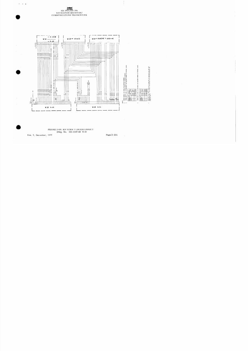
FIGURE 2 -8A
KN
73 /KN 77 INTERCONNECT
(Dwg. No.
155-1117-00 R-3)
Rev. 2, December, 1972
Page 2-13A
8/9/2019 KX 170A - Maintenance Manual Honeywell
http://slidepdf.com/reader/full/kx-170a-maintenance-manual-honeywell 42/586
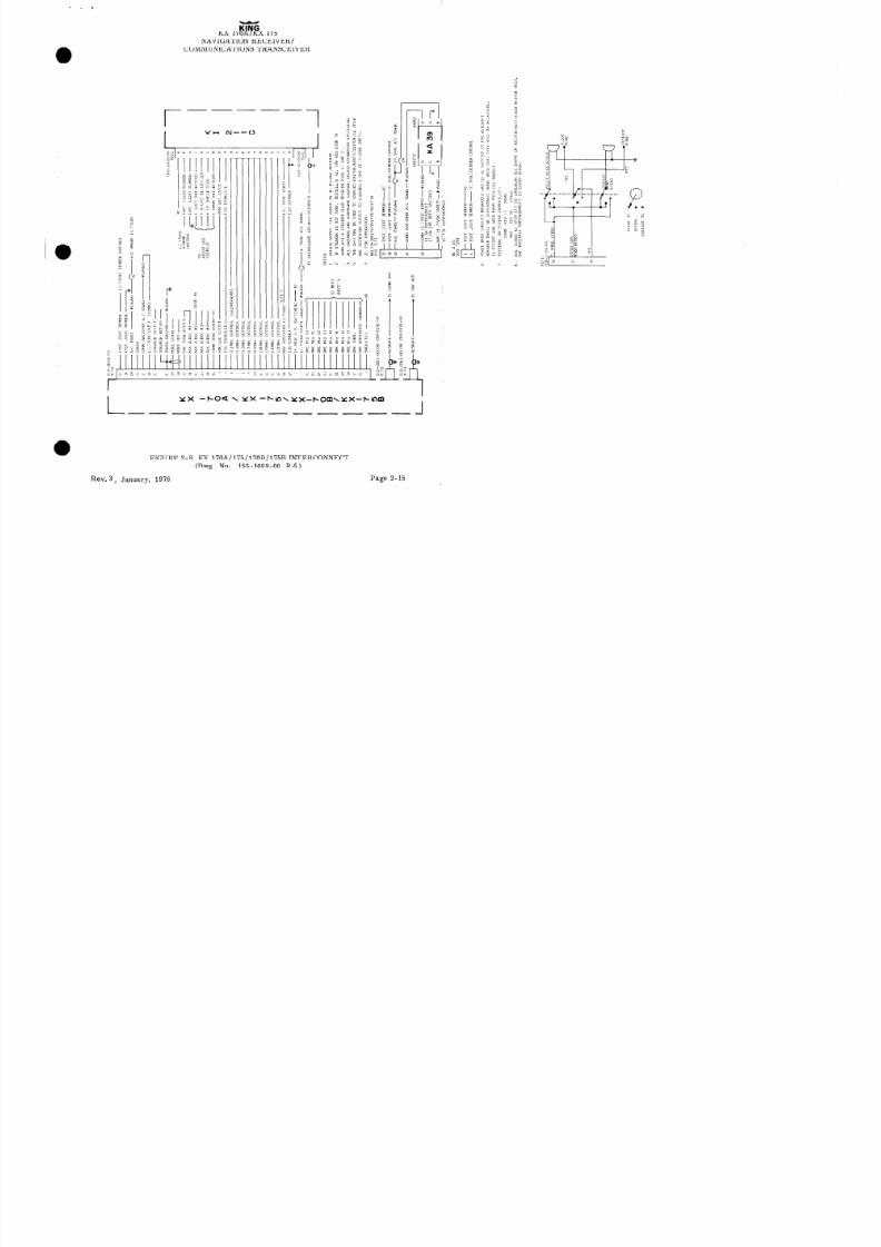
KI G
KX 170A
7
X 175
NAVIGATION RECEIVER /
COMMUNICATIONS TRANSCEIVER
XX
-boa\xx
-~ln\xx-~0om\YX-~uxn
FIGURE 2-9 KX 170A/175/17 0B/175B INTERCONNECT
(Dwg. No. 155-1089-00 R-5)
Rev.
3, January,
1976
Page 2-15

8/9/2019 KX 170A - Maintenance Manual Honeywell
http://slidepdf.com/reader/full/kx-170a-maintenance-manual-honeywell 43/586
KI G
7
X 170A KX 175
NAVIGATION RECEIVER
/
COMMUNICATIONS TRANSCEIVER
l-
------~--~---~~~
-I
FIGURE 2-10 NON-TSO’D SILVER CROWN SYSTEM INTERCONNECT
(Dwg. No.
155-1090-00 R-8)
Rev. 3, January, 1976 Page 2-17

8/9/2019 KX 170A - Maintenance Manual Honeywell
http://slidepdf.com/reader/full/kx-170a-maintenance-manual-honeywell 44/586
KlNG
KX 170A/KX 175
NAVIGATION RECEIVER/COMMUNICATIONS TRANSCEIVER
NOTE
DUCK
TAPE
NO1E 2
FINAL ASSY
NOTES:
I . MAKE ONE OF EACH PART SHOWN
2. POP RIVET TOGETHER 6 PLCS.
~ , 5 oo , 3 75 D IA . H OL E 3 0 P LC S.-
,/I30 DIA. HOLE 4 PLC;
9 SPACES EACH 1.000 APART = 9.000
3. POP RIVET RAM AIR TUBE TO DIFFUSER
HOUSNG
4. DUCK TAPE ALL SEAMS OF DIFFUSER.
AND SEAL IN TUBE
5 . T H E L EN GT H O F D IF FU SE R, A ND N UM BE R
O F H OL ES . D EP EN DS O N T HE H EI GH T O F
RADIO STACK OR AIRCRAFT PANEL
6. SEE SHEET 2 FOR SUGGESTED
INSTALLATION.
‘NOTES 3 84
I
+
625
PART C
.
l
3 000 -7000 I
.
9000
1
.
11.000
I
r.625 DIA. HOLE
PART A
--
7
.000
2.500
Al-
A
I
/r
m A
Y
'I
I
FIGURE 2-11 COOLING DIFFUSER FOR RADIO STACKS
Rev 3, January 1976
.I30 DIA. HOL
E/
4 PLCS
.I26 DIA. HOLE
4 PLCS
R4RT B
,093 D IA. HOLE 2 PLCS
M OU NT N G O F U N T O PT IO NA L, TO
INSTALLER.
\ BE ND ‘ BE ND U P T O M AK E
END
Page 2-19

8/9/2019 KX 170A - Maintenance Manual Honeywell
http://slidepdf.com/reader/full/kx-170a-maintenance-manual-honeywell 45/586
KlNG
KX 170A/KX 175
NAVIGATION RECEIVER/COMNIUNICATIONS TRANSCEIVER
, PANEL
KX 1758
KX 1758
KAl6 RAM AI R KI T
(150-0063-00)
TYPICAL INSTALLATION
KAl6-KPN(071-4001-00) AND DIFFUSER STACK
FIGURE 2-12 KR 16 RAM AIR KIT AND DIFFUSER INSTALLATION
Rev. 3, January, 1976
Page 2-21
AJRCRAFT-
SKIN
BEND TABS OVER MANIFOLD
WHEN MANIFOLD IS POSITIONEN
S HO WN ( RI GH T S ID E SH OW N T H
U NT M AY B E M OU NT ED lB O” T HA
047-1146-00
DRAIN HOLE
D UC T T U BI NG
150-0063-00
VIEW B
I NC LU DI NG E ND S O += M OU NT N G S C RE W S
WI TH A ZI NC CHROMATE SEALER.• R
EQUIVALENT.
u JN ~~~ ws $w N T UR NE D 1 80 ’ F RO M

8/9/2019 KX 170A - Maintenance Manual Honeywell
http://slidepdf.com/reader/full/kx-170a-maintenance-manual-honeywell 46/586
KING
KX 170A/KX 175
NAVIGATION RECEIVER/
COMMUNICATIONS TRANSCEIVER
SECTION
OPERATION
3.1 GENERAL
All controls required to operate the KX 170A/KX 175 and the KI 201C/211C are located
on the unit front panels.
3.2 KX 170AIKX175 NAV/COMM ONTROLS
3.2.1 COMM ON-OFF TEST CONTROL
The ON-OFF-TEST control is located directly above the COMM channel selector.
Power is supplied to the COMM when this control is either in the ON or TEST position.
The TEST position is used to defeat the COMM automatic squelch for both test purposes
and listening to extremely weak signals.
3.2.2 COMM VOLUME CONTROL
The Volume (VOL) control, located on the lower left side of the KX 170A/KX 175 is
used to adjust the transceiver audio volume. The KX 170A/KX 175 system power ON/
OFF switch is independent of this control, allowing the COMM volume to remain at a
desired preset level.
3.2.3 COMM FREQUENCY SELECTOR
The two concentric knobs under the COMM frequency window are used to dial COMM
frequencies. The larger knob selects MHz and the smaller knob selects kHz. The
transceiver is inoperable in the two unused MHz positions between 118MHz and 135MHz.
Clockwise rotation selects higher frequencies. The dial mechanism has no stops, per-
mitting continuous rotation.
3.2.4 NAV OFF-VOICE-IDENT CONTROL
The OFF-VOICE-IDENT control is located directly above the NAV channel selector.
Power is supplied to the NAV when this control is either in VOICE or IDENT position.
NAV operation is independent of COMM. With- the switch on IDENT, the ground station
voice and identification tone are coupled to the aircraft speaker and/or headphone cir-
cuitry. With the switch on VOICE the identification tone is eliminated, permitting the
pilot to monitor the VOR ground station for voice transmissions without receiving the
VOR ident tone.
March, 197 1
Page 3-l

8/9/2019 KX 170A - Maintenance Manual Honeywell
http://slidepdf.com/reader/full/kx-170a-maintenance-manual-honeywell 47/586
KING
KX 170A/KX 175
NAVIGATION RECEIVER/
COMMUNICATIONS TRANSCEIVER
3.2.5 NAV VOLUME CONTROL
The navigation receiver volume (VOL) control,
on the right side of the KX 170A/
KX 175, is used to control the level of the audio and/or identification tone output from
the navigation receiver.
This control is also independent of the system power switch
allowing the NAV volume to remain at a desired preset level.
3.2.6 NAV FREQUENCY SELECTOR CONTROLS
The two concentric knobs under the NAV frequency window are used to dial NAV freq-
uencies. The larger knob selects MHz and the smaller knob kHz. Clockwise rotation
selects higher frequencies.
Remote DME, Glideslope, and ILS channeling are also
performed by this control.
COMM. FREQUENCY READOUT
MHz FREQUENCY SELECTOR
I
KHz FREQUENCY SEL,ECTOR
I
NAV. FREQUENCY READOUT
COMM. VOLUME
NAV. t0Lu~~
KHz FREQUENCY SELECTOR
696-6006-00
MHz FREQUENCY SELECTOR
FIGURE 3- 1 KX 170A/ 175 CONTROL FUNCTIONS
Page 3-2
March, 197 1

8/9/2019 KX 170A - Maintenance Manual Honeywell
http://slidepdf.com/reader/full/kx-170a-maintenance-manual-honeywell 48/586
KI G
7
X 170A KX 175
NAVIGATION RECEIVER /
COMMUNICATIONS TRANSCEIVER
3.3 KI 201C/KI 211C NDICATORONTROLNDFUNCTION
3. 3.1 OMNI BEARING SELECTOR (OBS)
The Omni Bearing Selector knob rotates the azimuth card on which the desired course
is selected. The course selected serves as a reference for all VOR indications.
3. 3.2 VOR/LOC DEVIATION INDICATOR
The VOR/LOC deviation needle indicates the direction and amount of deviation from the
selected VOR course or localizer path.
The angular deviation is toward the proper
flight path in normal operation.
The VOR/LOC warning flag is fully visible when the VOR or LOC signal is unreliable.
The VOR TO/ FROM flag indicates the direction “to” or “from” the VOR station.
3. 3. 3 GLIDESLOPE DEVIATION INDICATOR (KI 211C)
The glideslope deviation needle indicates the direction and amount of deflection from
the glide path.
The deflection is toward the direction of flight required to maintain
the proper decent path.
The glideslope warning flag is visible when the glideslope
signal is unreliable or the receiver has malfunctioned.
COURSE INDEX
I
V OR i LOC
.~ARNING
FLAG
GLIDE SL
DEVIATI(
GLIDE SLOPE
WARNING FLA
.OPE
)N INDICATOR
.G
VOR/LO(‘
-DEVIATION
INDICATOR
\TO- FROM
FLAG
OMNI
BEARING
SELECTOR
696-6007-00
FIGURE 3-2 KI 20 l/2 11C CONTROL FUNCTIONS
Page 3-3

8/9/2019 KX 170A - Maintenance Manual Honeywell
http://slidepdf.com/reader/full/kx-170a-maintenance-manual-honeywell 49/586
KING
KX 170A/KX 175
NAVIGATION RECEIVER/
COMMUNICATIONS TRANSCEIVER
3.4 KI 201C/KI 211COPERATION
3.4.1 VOR OPERATION
Select the desired VOR station frequency with the NAV frequency controls.
The NAV
receiver volume control can then be adjusted to positively identify the station or listen to
FSS reports.
To intercept a selected VOR radial (from the station) and fly outbound, turn the OBS
control to set the desired radial under the top indicator index. Maneuver the aircraft
to fly the selected radial magnetic heading plus a 45” intercept angle which will provide
a sufficient intercept angle.
The intercept angle should be reduced as the deviation
needle approaches an on course condition (center) to prevent excessive course bracket-
ing.
To determine the bearing and fly “to” a selected VOR station, turn the OBS control until
the “To-From” flag indicates
“To” and the deviation needle is centered. Read the “to”
bearing under the top indicator index and maneuver the aircraft to approximately fly the
magnetic course “to” the station. If the deviation needle moves to the right, the aircraft
course must be adjusted 5 or 10 degrees to the right. Similarly, if the deviation needle,
goes to the left, the aircraft course must be adjusted to the left. Maintaining a centered
deviation needle will provide automatic course compensation for wind drift.
While flying a selected VOR course often times it can be noted that the deviation needle
moves erratically about the center or moves a few degrees to one side and eventually
returns to center.
This action is refered to as VOR scalloping or course bends.
Scalloping is generally caused by irregularities in terrain and metal objects located near
the VOR station.
Scalloping is more noticable at lower altitudes and in any case should
be ignored.
Aircraft position can be easily determined by consecutively selecting two VOR stations
and determining the “from” radial. By projecting appropriate radial lines from the VOR
station the aircraft location may be identified as the intersection of the two radial lines.
3.4.2 KI 20 1C /KI 2 11C LOCALIZER OPERATION
Localizer circuits are automatically energized when an ILS frequency is selected on the
KX 170A/KX 175 NAV receiver.
By adjusting the NAV volume level the localizer station
can be identified and in some cases ATIS information received. The localizer flag
should disappear from view indicating the signal is reliable.
Maneuver the aircraft to fly an on course centered needle.
While flying a front course
approach or out bound on the back course approach, magnetic heading corrections are
Page 3-4
March, 197 1
l

8/9/2019 KX 170A - Maintenance Manual Honeywell
http://slidepdf.com/reader/full/kx-170a-maintenance-manual-honeywell 50/586
KI G
r
X 170A
KX 175
NAVIGATION RECEIVER /
COMMUNICATIONS TRANSCEIVER
made toward the needle deflection.
Similarly, while flying the back course approach
or outbound on the front course approach, corrections are made away from the needle
deflection.
The localizer course width is narrow compared to VOR course width and requires much
smaller course corrections to center the deviation needle.
When intercepting the
localizer course, the aircraft turn into the localizer course should be started when the
needle moves off the meter stop.
A helpful quick reference reminder of the localizer course is to set the course on the
Omni bearing readout.
3.4.3
KI 2 11C GLIDESLOPE OPERATION
The glideslope (horizontal) needle provides the pilot vertical steering information
during ILS approaches. The glideslope circuitry is energized when the associated
localizer frequency is selected on the navigation receiver, observe that the glideslope
warning flag is concealed.
The glideslope needle deflects toward the direction the
pilot must fly to remain on the glideslope. If the glideslope needle deflects upward the
aircraft is below the glideslope and must climb to center the needle.
If the needle
deflects downward the aircraft is above the glide path and must descent to remain on
the glide path. When the needle is centered the aircraft is on the glide path.
3.5 POST-INSTALLATIONHECKOUT
An operational performance flight test is recommended after the installation is com-
pleted to insure satisfactory performance of the equipment in its normal environment.
To check the communications transceiver, maintain an appropriate altitude and contact
a ground station facility at a range of at least fifty nautical miles. Contact a ground
station close in. Place the squelch knob in the test position and listed for any unusual
electrical noise which would reduce the COMM receiver sensitivity by increasing the
squelch threshold. If possible, verify the communications capability on both the HIGH
and LOW ends of the VHF COMM band.
To check the VOR/ILS System select a VOR frequency within a forty nautical mile range.
Listen to the VOR audio and insure that no electrical interference such as magneto noise
is present.
Check the tone identifier filter operation.
Fly inbound or outbound on a
selected VOR radial and check for proper LEFT-RIGHT and TO-FROM indications.
Check the VOR accuracy.
-NOTE-
At low altitudes VOR ground station
scalloping may be present.
March, 197 1
Page 3-5

8/9/2019 KX 170A - Maintenance Manual Honeywell
http://slidepdf.com/reader/full/kx-170a-maintenance-manual-honeywell 51/586
KING
KX 170A/KX 175
NAVIGATION RECEIVER/
COMMUNICATIONS TRANSCEIVER
Flight test the ILS operation by flying a simulated ILS approach.
Check localizer
LEFT-RIGHT deflection and, if applicable, glideslope deflection. Check the localizer
accuracy in relation to the ILS runway. Check the glideslope accuracy in relation to
the published ILS approach altitude.
Page 3-6
March, 197 1
0

8/9/2019 KX 170A - Maintenance Manual Honeywell
http://slidepdf.com/reader/full/kx-170a-maintenance-manual-honeywell 52/586
I
MAINTENANCE/OVERHAUL
MANUAL
KX 17OA/KX 75
NAV/COMM
TRANSCEIVER
KING RADIO C~FW~RATION,
‘i
400 NORTH ROGERS ROAD
OLATHE, KANSAS, U.S.A.

8/9/2019 KX 170A - Maintenance Manual Honeywell
http://slidepdf.com/reader/full/kx-170a-maintenance-manual-honeywell 53/586
KING
KX 170A/KX 175
NAVIGATION RECEIVER/
COMMUNICATIONS TRANSCEIVER
TABLEOF CONTENTS
Paragraph
Page
SECTIONV THEORY F OPERATION
4
General
4-1
4.2
Frequency Synthesizers
4-l
4. 2. 1
SMO Block Diagram
4-l
4.2.2
SMO Circuit Theory
4-7
4.3
COMM Transceiver
4-29
4. 3. 1
Block Diagram Theory
4-29
4.3. 2
COMM Transceiver Circuit Theory
4-30
4.4
NAV Receiver
4-37
4.4. 1
Block Diagram Theory
4-37
4.4. 2
NAV Receiver Circuit Theory
4-37
4.5 KA 39 Voltage Converter 4 -40
5. 1
Test Equipment
SECTION MAINTENANCE
5-l
5. 2
5. 2. 1
5-2
5-2
5. 2.2
5-4
5. 2. 3
5. 2.4
5-6
5-8
5. 2. 5
5. 2. 6
Alignment and Test Procedure
NAV SMO Alignment and Test
(SMO and Voltage Regulator)
COMM SMO Alignment and Test
(SMO and Voltage Regulator)
NAV/COMM Receiver Preliminary Alignment & Test
NAV Receiver Alignment
(VOR / LOC Adjust)
COMM Receiver Alignment
(Carrier/Noise SQ and Carrier SQ Adjust)
Transmitter Alignment
(Mike Gain and Sidetone Level Adjust)
Notes : Standard Signals
Final Test Data
5-10
5-12
5. 2.7
5. 2. 8
5-13
5-17
5. 3
General Maintenance
5-22
5. 4
Troubleshooting the KX 170A/KX 175
5-31
5. 5
Troubleshooting the NAV SMO
5-43
5. 5. 1
Preliminary Evaluation
5-44
5. 5.2
NAV SMO Diagnostic Procedure
5-44
5. 6
Troubleshooting the COMM SMO
5-64
5. 6. 1 Preliminary Evaluation
5-65
5. 6. 2 COMM SMO Diagnostic Procedure
5-65
5. 7 Troubleshooting the NAV Receiver
5-89
5.7.1
Preliminary Evaluation
5-89
5. 8
Troubleshooting the COMM Receiver
5-105
5.8. 1
Preliminary Evaluation
5-105
5.9
Troubleshooting the Audio Amplifier
5-123
8/9/2019 KX 170A - Maintenance Manual Honeywell
http://slidepdf.com/reader/full/kx-170a-maintenance-manual-honeywell 54/586
KI G
r
X 170A KX 175
NAVIGATION RECEIVER/
COMMUNICATIONS TRANSCEIVER
TABLEOFCONTENTS
Paragraph
5. 10 Troubleshooting the Transmitter
5. 11
Troubleshooting the Regulators
5. 12
Troubleshooting the KA 39 Voltage Converter
Item
1.
2.
3.
4.
5.
6.
‘7.
8.
9.
10.
11.
12.
13.
14.
15.
Figure
4-l KX 170A/175 Simplified SMO Block Diagram
4-2
4-2
Typical Loop Transfer Function
4-3
4-3 Balanced Mixer
4-8
4-4
Mixer Low Pass Filter
4-9
4-5
Squaring Amplifier
4-9
4-6
400 KHz Reference Oscillator
4-10
4-7
Typical Gate Circuits
4-11
4-8
Basic Logic Function
4-12
4-9 Reset and Preset Counters 4-13
4-10
9300 Logic
4-16
Page
5-127
5-133
5-134
SECilONVI ILLUSTRATEDARTS IST
KX 170A/KX 175
Front Plate Sub-Assembly
Switch Head Sub-Assembly
Nav. SMO Board Sub-Assembly
Nav. SMO Sub -Assembly
COMM SMO Board Sub-Assembly
COMM SMO Sub-Assembly
NAV /COMM Board Sub-Assembly
Transmitter Assembly
Rear Plate Assembly
Audio Drive Board Assembly
Rear Divider Sub-Assembly
Conn. Cable Sub-Assembly
Voltage Converter - KA 39
KX 170A
Page
6-l
6-3
6-7
6 - 17
6-26
G-29
6-39
6-42
6-54
6-58
6-61
6-64
6-68
6-71
6-75
LISTOF ILLUSTRATIONS
Page
ii

8/9/2019 KX 170A - Maintenance Manual Honeywell
http://slidepdf.com/reader/full/kx-170a-maintenance-manual-honeywell 55/586
Figure
4-11
4-12
4-13
4-14
4-15
4-16
4-17
4-18
4-19
4-20
4-21
4-22
4-23
4 -24
4-25
4-26
4-27
4 -28
4-29
4-30
4-31
5-l
5-2
5-3
5-4
5-5
5-6A
5-6B
NAV SMO Test Point and Alignment Locations
COMM SMO Test Point and Alignment Locations
NAV and COMM Voltage Regulators
NAV VCO Tuning Adjustment Location
NAV Ident Filter Adjustment Location
Receiver Alignment Loading Point
Receiver Test Point and Alignment Locations
5-7A&B Transmitter Alignment and Audio Board Adjustment Locations
5-7c Test Circuit
5-8 Microphone Gain Adjust Detector Waveforms
5-9 Detector Schematic
5-10
RF Attenuator Schematic
5-11
KX 17OA/KX 175 Bench Test Setup
5-12
Troubleshooting Flow Chart
5-13
Low Reference Oscillator Output
5-14 Mixer Output
5-15 Squaring Amplifier Output
5-16
Programmable Divider Output
KX 1 01 +X 175
N)
NAVIGATION RECEIVER/
COMMUNICATIONS TRANSCEIVER
TABLEOFCONTENTS
Basic Phase and Frequency Comparator System
Voltage Translator Circuit
Simplified Programmable Divider, Phase and Frequency Comparator
Typical Wave Forms VCO Low Pass Filter
VCO Low Pass Filter
Basic VCO Principles
NAV VCO
COMM VCO
COMM SMO Buffer Amplifier
Implicit Divide by 2
NAV Implicit Divide by 2 Circuit
COMM Implicit Divide by 2 Circuit
Simplified Colpitts Oscillator
High Reference Oscillators
Simplified Pierce Oscillator
Second IF Integrated Circuit Schematic
COMM AGC System
Input Power Line Filter
Regulator Schematic
NAV AGC System
KA 39 Voltage Converter Schematic
Page
4-18
4-19
4-20
4-21
4-22
4-22
4-23
4-24
4-25
4-26
4-26
4-27
4-27
4-28
4-30
4-31
4-32
4-35
4-36
4-39
4 -40
5-2
5-4
5-5
5-6
5-8
5-11
5-11
5-13
5-13
5-14
5-15
5-15
5-16
5-30
5-45
5 -46
5-47
5 -48
iii

8/9/2019 KX 170A - Maintenance Manual Honeywell
http://slidepdf.com/reader/full/kx-170a-maintenance-manual-honeywell 56/586
Figure
5-17
5-18
5-19
5-20
5-21
5-22
5-23
5-24
5-25
5-26
5-27
5-28
5-29
5-30
5-31
5-32
5-33
5-34
5-35
5-36
5-37
5-38
5-39
5 -40
5-41
5-42
5-43
5 -44
5-45
5-46
5-47
5 -48
KI G
KX 170A
7
KX 175
NAVIGATION RECEIVER/
COMMUNICATIONS TRANSCEIVER
TABLEOFCONTENTS
Voltage Translator
Programmable Divider
NAV Low Ref. Osc. /Programmable Div. /Phase and Frequency
Comparator
VCO Buffer
NAV High Ref. Osc. , Implicit i 2 Circuit, 2nd Mixer, Mixer Low
Pass Filter, Squaring Amplifier
Low Ref. Oscillator output
‘Mixer Output
Squaring Amplifier Output
Programmable Divider Output
Voltage Translator
Programmable Divider
COMM Programmable Divider/Phase and Frequency Comparator
COMM Voltage Controlled Oscillator/VCO Low Pass Filter/25 KHz
Voltage Translator /VCO Buffer /Transmit Buffer /Transmit Enable
.Switch Out-of-Lock Transmit D isable
C OMM High Reference Oscillator/Implicit t 2 Circuit / 2nd Mixer /
Mixer Low Pass Filter /Squaring Amplifier
Timing Diagram Programmable Divider
Timing Diagram Phase and Frequency Comparator
AGC Amplifier DC Characteristics
Detector Setup
NAV Preselector/RF Amplifier/lst Mixer/lst IF.
NAV 2nd Local Oscillator, 2nd Mixer, and 2nd IF
NAV DET. /Noise Limiter/AGC Amplifier/Ident. Filter and Audio
Amplifier
\
AGC Amplifier DC Characteristics
Detector Test Setup
COMM Preselector, R. F. Amplifier,
1st Mixer and 1s t I. F.
COMM 2nd L. 0. ,
2nd Mixer, 2nd I. F. and Detector
NAV Detector /Noise Limiter /AGC Amplifier Audio Preamplifier
COMM Squelch Gate, Noise Amplifier and Filter, Carrier to Noise
Squelch and Carrier Squelch
Summing Junction, T-R Diode Switch, Audio Pre-Driver, Audio
Driver, Audio Output Amplifier
Final Amplifier
Regulators
NAV Block Diagram
Page
5-49
5-51
5-55
5-59
5-62
5-66
5-67
5-68
5-69
5-70
5-72
5-75
5-79
5-83
5-85
5-87
5-89
5-90
5-94
5-98
5-102
5-105
5-106
5-110
5-113
5-116
5-121
5-125
5-129
5-132
5-135
iv

8/9/2019 KX 170A - Maintenance Manual Honeywell
http://slidepdf.com/reader/full/kx-170a-maintenance-manual-honeywell 57/586
Figure
Page
5-49 COMM Block Diagram 5-137
5-50 NAV SMO Schematic
5-139
5-51
C OMM SMO Schematic
5-141
5-52 NAV /COMM Receiver Schematic
5-143
5-53
Transmitter /Audio Schematic
5-145
5-54
Switching Assembly Schematic
5-147
5-55
KY 195 Switching Assembly Schematic
5-149
5-56
KA 39 Voltage Converter Schematic
5-151
KING
KX 170A/KX 175
NAVIGATION RECEIVER /
COMMUNICATIONS TRANSCEIVER
TABLE FCONTENTS
6-l Front Plate Assembly
6-2
Switch Head Sub-Assembly
6-2A
SW+ c h Head Sub -Assembly
6-3A
6-3B
6 -3C
6-4
6-5A
6 -5B
6-5C
6-6
6 -7A
6 -7B
6-7C
6-8
6-9
6-10
6-11
6-12
TABLES
No.
NAV SMO Board Assembly
NAV SMO Board Assembly
NAV SMO Board Assembly
NAV SMO Board Assembly
COMM SMO Board Assembly
COMM SMO Board Assembly
COMM SMO Board Assembly
C OMM SMO Sub-Assembly
NAV /COMM Board Sub -Assembly
NAV/COMM Board Sub-Assembly
NAV /COMM Board Sub-Assembly
Transmitter Assembly
Rear Plate
Audio Board Sub-Assembly
Rear Divider Sub-Assembly
KA 39 Voltage Converter
4-l T-R Switching Requirements
4-5
4-2 Frequencies Appearing in the KX 170A/KX 175 4-6
4-3 NAV Programmable Counter Coding
4-14
4-4 COMM Programmable Counter Coding
4-15
6-5
6 -13
6-15
6-23
6-24
6-25
6-28
6-36
6-37
6-38
6-41
6-50
6-51
6-52
6-56
6-59
6-62
6-66
6:74
Page
V
8/9/2019 KX 170A - Maintenance Manual Honeywell
http://slidepdf.com/reader/full/kx-170a-maintenance-manual-honeywell 58/586
Figure
5-l
5-2
5-3
5-4
5-5
5-6
.5-7
5-8
5-9
5-10
5-11,
5-12
5-13
5-14
KX 17% l l 175
NAVIGATION RECEIVER/
COMMUNICATIONS TRANSCEIVER
TABLEOFCONTENTS
NAV Channel-SMO Frequency-VCO Tuning Voltage
COMM Channel -Receive SMO Frequency-VCO Tuning Voltage
NAV Channel-SMO Frequency-Receiver Tuning Voltage
COMM Channel-Receive SMO Frequency-Tuning Voltage
NAV SMO Trouble Chart
COMM Receiver Trouble Chart
NAV Receiver Trouble Chart
COMM Receiver Trouble Chart
COMM Transmitter Trouble Chart
NAV SMO Synthesizer Frequencies
COMM SMO Synthesizer Frequencies
High Reference Oscillator Troubleshooting Table
NAV Stage Gain Chart
COMM Stage Gain Chart
Page
5-3
5-5
5-6
5-7
5-32
5-34
5-37
5-39
5-41
5-43
5-64
5-81
5-91
5- 107
vi

8/9/2019 KX 170A - Maintenance Manual Honeywell
http://slidepdf.com/reader/full/kx-170a-maintenance-manual-honeywell 59/586
KING
KX 170A/KX 175
NAVIGATION RECEIVER/
COMMUNICATIONS TRANSCEIVER
The information in this maintenance manual does not profess to include all the details
of design, production, or variations of the equipment, or to cover all the possible
contingencies which may arise during operation, installation, or maintenance. Should
special p roblems arise or further information be desired, please contact the KING
Customer Service Department.
vii

8/9/2019 KX 170A - Maintenance Manual Honeywell
http://slidepdf.com/reader/full/kx-170a-maintenance-manual-honeywell 60/586
KX 17OyE 175
NAVIGATION REC EIVE R /
COMMUNICATIONS TRANSCEIVER
FIGURE l-l KX 17OA/KX 175
viii

8/9/2019 KX 170A - Maintenance Manual Honeywell
http://slidepdf.com/reader/full/kx-170a-maintenance-manual-honeywell 61/586
Ki G
7
X 170A KX 175
NAVIGATION RECEIVER/
COMMUNICATIONS TRANSCEIVER
SECTIONV
THEORY FOPERATION
4.1 GENERAL
The KX 170A/KX 175 unit incorporates a 200 channel navigation receiver, a 360 channel
communications transceiver and a 5 watt audio system.
The KI 20 1C is an OMNI/ LOC
converter and indicator.
The KI 211C includes the KI 201C capability plus a 20 channel
glideslope receiver with indicator.
The KA 39 is a dual series regulator, Zeparately
converting 27. 5VDC to 13.75VDC for the COMM and NAV.
For discussion purposes, the KX 170A/KX 175 system is split into subsystems and
treated on the basis of block diagram theory and detailed circuit theory.
Subsystems
are defined as Frequency Synthesizers (COMM and NAV), COMM Transceiver, NAV
Receiver and KA 39 Voltage Converter.
4.2 FREQUENCYYNTHESIZERS
4. 2. 1
SMO BLOCK DIAGRAM
4. 2. 1. 1
Simplified Block Diagram.
The KX 17OA/KX 175 uses a stabilized master oscillator (SMO) for frequency generation.
A feedback loop is used to slave a voltage controlled oscillator (VCO) to the seiected
multiple frequency of a crystal controlled reference oscillator. The simplified block
diagram of Figure 4-l illustrates the principle of operation of the COMM SMO and NAV
Sxif ).
‘i‘he \/CO output frequency is divided by two,
mixed with the High Frequency Crystal
<>scillator, divided by N, and compared in frequency and phase with the Low Frequency
Crystal Oscillator.
The filtered error signal biases the VCO. The error signal is a
5 high voltage when the VCO frequency is low and a low voltage when the VCO frequency
is above the desired frequency.
According to the VCO transfer function (Figure 4 -2b)
this error signal drives the VCO toward the selected frequency.
When the VCO gets
within t400KIIz of the desired frequency,
the loop captures the VCO and pulls it into
phase lock (fVC0 =f selected). In this condition the loop establishes an error signal
that is a 25KHz square wave. The low pass filter recovers the dc component and biase,:
the VCO to maintain the selected output frequency.
The square wave duty factor, and
thus the filtered D-C VCO bias voltage,
varies according to the selected VCO frequency.
Transfer functions of the various blocks are illustrated in Figure 4-2.
March, 197 1
Page 4-l

8/9/2019 KX 170A - Maintenance Manual Honeywell
http://slidepdf.com/reader/full/kx-170a-maintenance-manual-honeywell 62/586
KI G
7
X 170A
KX 175
NAVIGATION RECEIVER /
COMMUNICATIONS TRANSCEIVER
r
4
LOW
FREQ.
CRYSTAL
osc.
fLF
L
O0
v
PHASE
AND
FREQ.
ERROR
SIGNAL
LOW
PASS
FILTERED r
ERROR
VOLTAGE
OUTPUT FREQ.
SIGNEL
w CONTROLLED-
e
f,= 2(fHF-NfLF)
*
COMPARATOR
FILTER
osc.
1
4
I
FREOUENCY NfLF
fHF-NfLF FREQUENCY
MIXER 4 c-
‘,N
,2
L
b A +
A
fHF
WAFER
SW ITCHES
696-6008 -00
FIGURE 4-l KX 170A/KX 175 SIMPLIFIED SMO BLOCK DIAGRAM
Page 4-2
March,
1971
0

8/9/2019 KX 170A - Maintenance Manual Honeywell
http://slidepdf.com/reader/full/kx-170a-maintenance-manual-honeywell 63/586
Kx 17m 175
March, 197 1
NAVIGATION RECEIVER/
COMMUNICATIONS TRANSCEIVER
A) TYPICAL LOW PASS FILTER FREQ. RESPONSE
I
I
IO KHz 25 KHz
FREQUENCY
B) TYPICAL VCO TRANSFER FUNCTION
C) PHASE AND FREQ. COMPARATOR
W
8
5
9
HIGH DC
t
PHASE LOCK
(25KHz SO. WAVE)
LOW DC
I
fDESlRED FREQ.
696-6009-00
FIGURE 4-2 TYPICAL LOOP TRANSFER FUNCTIONS
Page 4-3

8/9/2019 KX 170A - Maintenance Manual Honeywell
http://slidepdf.com/reader/full/kx-170a-maintenance-manual-honeywell 64/586
KX 17 ?
K?
x 175
NAVIGATION RECEIVER /
COMMUNICATIONS TRANSCEIVER
4.2. 1.2 NAV SMO Block Diagram.
The NAV SMO is a 200 channel frequency synthesizer covering the band from 92.8 125 -
102. 7625MHz in 5OKHz steps.
The block diagram is the red shaded portion of Figure
5-48. The basic frequencies appearing in the NAV SMO are tabulated in Table 4-2 and
also appear on the block diagram.
The VCO converts a dc bias voltage to a VHF frequency. The,buffer amplifiers isolate
the VCO from reverse conducted electrical interference signals and provide .lOmw out-
put levels for mixer injection.
The Implicit Divide by Two circuit halves the VCO
frequency. A mixer is used to heterodyne the halved VCO frequency and the High
Frequency Rekference Oscillator.. The Mixer Low Pass Filter passes the difference
frequency and filters any spurious mixer products. In the Squaring Amplifier the analog
difference frequency is amplified and clipped to provide a 4. 5V square wave.
The
Programmable Divider generates one output pulse for every N input pulses. Selection
of the divide ratio, N, is determined by the wafer switch coding. The 400KHz Reference
Oscillator is divided by 16 in the Phase and Frequency Comparator block to obtain a
25KHz reference. This block also compares the Programmable’Counter output in fre-
quency and phase with the 25KHz reference frequency and generates an appropriate
feedback signal to slew the loop until This variable frequency is locked to the 25KHz
reference.
The Voltage Translator shifts the level of the error voltage from the Phase
and Frequency Comparator. The VCO Low Pass Filter is used to recover the D-C
component of the phase ‘detected, variable duty cycle,
25KHz square wave and to provide
Fteady state and dynamic loop stabilization.
The formula for the synthesized frequency
is: fL;CO =2 (53. 93125 - .025N) MHz where N may be any number from 102 to 30 1.
4
.2, 1.2
COMM SMO Block Diagram.
T le CCMM SMO is a 360 channel, frequency synthesizer covering the band of frequencies
from 118.00 to 135.95MHz in 50KHz steps.
The block diagram is the red shaded portion
of figure 5-49.
The basic frequencies appearing in the COMM SMO are tabulated in
Table 4 -2 and also appear on the block diagram.
13asic theory of the NAV SMC (Section 4. 2. 1. 2) applies to the COMM SMO.
In order to
obtain 360 channels and transmit-receive sidestep transitions, the COMM band is split
into two 9MEIz Bands (118.00 - 126. 95MHz and 127. 00 - 135. 95MHz).
Requirements for
T/K switching are summarized in Table 4-l.
Page 4-4
March, 197 1

8/9/2019 KX 170A - Maintenance Manual Honeywell
http://slidepdf.com/reader/full/kx-170a-maintenance-manual-honeywell 65/586
KI
KX 170A
Y
KX 175
NAVIGATION RECEIVER /
COMMUNICATIONS TRANSCEIVER
Selected Band
Selected Band
118.00-126.95MHz
127.00-135. 95MHz
Transmit VCO=118.00-126.95MHz
VCO=127.00-135.95MHz
Receive VCO=127.00-135.95MHz VCO=118.00-126.95MHz
TABLE 4- 1 T-R SWITCHING REQUIREMENTS
March, 197 1
Page 4-5

8/9/2019 KX 170A - Maintenance Manual Honeywell
http://slidepdf.com/reader/full/kx-170a-maintenance-manual-honeywell 66/586
KING
r
NAV
l-
Selected Channel
(50KHz steps)
VCO Frequency
(5OKHz steps)
Implicit f 2 Freq
(25KHz steps
H. F. REF Frequency
Mix Output Frequency
Divide Ratio
L. F. REF Frequency
Approx. VCO Bias
Approx. Receiver
tuning voltage.
1st I. F. Frequency
2nd I. F. Frequency
2nd L. 0. Frequency
108.00 - 117.95MHz
92.8 125 - 102.7625MHz
46.40625 - 51.38 125MHz.
53.93 125MHz
7. 525 - 2. 550MHz
301 - 102
F = 25KHz
2.95 -
7. 20 volts
2.95 -
7.20 Volts
15. 1875MHz
1. 1857MHz
14.00 18MHz
C OMM
I
SMO HIGH BAND
118.00 - 126.95 R MHz
127.00 - 135. 95 T
127.00 - 135. 95MHz
63.500 - 67.975MHz
7 1.025MHz
7. 525 - 3.050MHz
301 - 122
F = 25KHz
2.50
- 7.00 Volts
SMO LOW BAND
I
118.00 - 126. 95MHz
59.000 - 63.475MHz
66.525MHz
7. 525- 3.05OMHz
301 - 122
400KHz
16
= 25KHz
2. 50 - 7.00 Volts
127.00 - 135.95 RMkz
118.00 - 126.95 T
2.95 - 7.80
9. OOOOMHz
861.2500KHz
8. 13875MHz
T-ABLE 4-2 FREQUENCIES APPEARING IN THE KX 170A/KX 175
Page 4-6
REV. 1, January, 1972

8/9/2019 KX 170A - Maintenance Manual Honeywell
http://slidepdf.com/reader/full/kx-170a-maintenance-manual-honeywell 67/586
KI G
7
X 170A
KX 175
NAVIGATION RECEIVER /
COMMUNICATIONS TRANSCEIVER
The phase locked loop synthesizes 180 channels in each 9MHz band and is switched be-
tween high and low bands with the High Reference Oscillator crystals and the VCO band
switch. This system provides 360 channels with a 180 digit counter and fast T-R transi-
tions without requiring special coding of the Programmable Divider.
Note that the
receiver uses a combination of high and low side injection and that the first I-F frequency
is restricted to 9. OMHz.
The Out of Lock Disable block turns off the receiver buffer and transmitter buffer when
the SMO is out of lock or is the receive condition.
The VCO is disabled in the two
unused MHz positions of the frequency selector.
Formulas for the synthesized frequencies are:
(Low band) fvCo =2 (66. 525 - .025N) MHz
(High band)
fvco
=2 (71.025 - .025N) MHz
where N is any selected number from 122 to 301.
4.2.2
SMO Circuit Theory
4.2.2. 1
Circuit Theory
Elements Common to NAV and COMM SMOS.
Due to the similarity in function, the
Mixer Low Pass Filter, Squaring Amplifier, Programmable Divider, Phase and
Frequency Comparator, Square Wave Voltage Translator, and VCO Low Pass Filter
circuitry is of common design in the NAV SMO and COMM SMO.
The differences in
counter divide ratios are handled in the COMM and NAV wafer switching.
The simi-
larity of design makes possible trouble shooting methods employing comparison
techniques. This is discussed in detail in Section V.
In the following discussion, NAV
schematic reference numbers appear without brackets and COMM schematic reference
numbers appear with brackets.
BALANCED MIXER
The balanced mixer configuration was chosen to minimize spurious generation and to
provide isolation between the digital circuitry, the VCO, and the high reference os-
cillator. The balanced mixer consists of transformers, T206 (T304), T207 (T306),
diode quad CR207 (CR309) thru CR210 (CR3121 and capacitors C232 (C364) and C233
(C365). Bifilar wound helical transformers and low capacitance, low noise, hot carrier,
mixer diodes are used to maintain mixer balance.
March, 197 1
Page 4-7
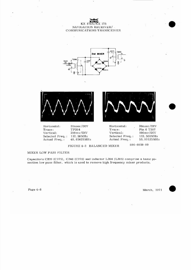
8/9/2019 KX 170A - Maintenance Manual Honeywell
http://slidepdf.com/reader/full/kx-170a-maintenance-manual-honeywell 68/586
KX 17F
Y?
x 175
NAVIGATION RECEIVER/
COMMUNICATIONS TRANSCEIVER
‘.
.a
Horizontal:
20nsec /DIV Horizontal: ,
20nsec /DIV
Trace : TP204
Trace:
Pin 6 T207
Vertical: 200mv/DIV
Vertical:
lOOmv/DIV
Selected Freq. : 112. 50MHz
Selected Freq. :
112.500MHz
Actual Freq. :
48.65625MHz
Actual Freq. :
53. 93 125MHz
FIGURE 4-3 BALANCED MIXER
696-6010-00
MIXER LOW PASS FILTER
Capacitors C239 (C375), C240 (C376) and inductor L204 (L305) comprise a basic pi-
section low pass filter, which is used to remove high frequency mixer products.
Page 4-8
March, 197 1
0

8/9/2019 KX 170A - Maintenance Manual Honeywell
http://slidepdf.com/reader/full/kx-170a-maintenance-manual-honeywell 69/586
KING
KX 17OA/KX 175
NAVIGATION RECEIVER/
COMMUNICATIONS TRANSCEIVER
MIXER LOW PASS
Horizontal :
O.O5psec/DIV
Trace: C241
Vertical:
50mV /DIV
Selected Freq. : 112. 50MHz
FIGURE 4-4 MIXER LOW PASS FILTER
696-6011-00
SQUAR.ING AMPLIFIER
Transistors Q208 (Q3 12) and Q209 (Q3 13) are used in a complementary configuration to
provide wide band amplification and clipping. The output waveform is a 4 volt square
wave as indicated in Figure4 -5.
Horizontal : O.O51.(sec/DIV Horizontal :
Trace: ’ Base Q208 Trace:
Vertical:
50mv/DIV Vertical:
Selected Freq. :
112. 5OMHz
Selected Freq. :
Actual Freq:
5. 275MHz Actual Freq:
FIGURE 4-5 SQUARING AMPLIFIER
O.O5psec/DIV
TP206
lV/DIV
112. 50MHz
5.275MHz
696-60 12-00
March, 197 1
Page 4-9

8/9/2019 KX 170A - Maintenance Manual Honeywell
http://slidepdf.com/reader/full/kx-170a-maintenance-manual-honeywell 70/586
KX 17F
17
KX 17j
NAVIGATION RECEIVER/
COMMUNICATIONS TRANSCEIVER
~OOKHZ REFERENCE
The low frequency reference oscillator and its waveform are illustrated in Figure 4-6.
Transistors Q210 (Q3 15) and Q211 (Q3 16) are connected as an astable multivibrator.
Crystal Y202 (Y303 KX 175: only) acts as a series resonant element controlling thk
oscillation of the multivibrator.
The 400KHz low frequency reference signal is applied
to both the COMM and NAV phase and frequency discriminator circuits.
R2.5
47K
a
211
L.F. REFERENCE OSC.
696-6013-00
FIGURE 4-6 400KHz REFERENCE OSCILLATOR
DIGITAL CIRCUITRY
A. LOGIC REVIEW
Two types of logic circuitry are used in the KX 170A, KX 175, these are, Resistor-
Transistor Logic (RTL) and Transistor-Transistor Logic (TTL). Typical gate
schematics are shown in Figure 4-7.
Typical supply voltages are 3. 6 volts for
RTL and 5.0 volts for TTL.
Basic gates and JK Flip Flop are defined symbolically
and functionally in Figure 4-8. In the KX 170A / KX 175 the Nand gates are TTL,
the Nor gates are RTL, and the J-K flip-flops are TTL.
Page 4-10
March, 197 1
e

8/9/2019 KX 170A - Maintenance Manual Honeywell
http://slidepdf.com/reader/full/kx-170a-maintenance-manual-honeywell 71/586
KI G
7
X 170A KX 175
NAVIGATION RECEIVER/
COMMUNICATIONS TRANSCEIVER
TTL
v
cc
ToUTpuT
March, 197 1
L
OUTPUT
NAND
GATE
NOR
GATE
696 -60 14 -00
FIGURE 4-7 TYPICAL GATE CIRCUITS
Page 4-11

8/9/2019 KX 170A - Maintenance Manual Honeywell
http://slidepdf.com/reader/full/kx-170a-maintenance-manual-honeywell 72/586
zitz
KX 17OA/KX 175
NAVIGATION RECEIVER/
COMMUNICATIONS TRANSCEIVER
I.
GATES
A. 5
Inputs
outputs
All high (1)
Low (0)
Any low (0)
High (1)
B.
NOR
All low (0)
High (1)
Any high (1)
Low (0) 0
c
J.
AND
All high (1)
High (1)
Any low (0) Low (0)
D.
0 K
All low (0)
Low (0)
Any high (1)
High (1)
II.
CLOCKED J-K FLIP FLOPS
RTL
s c
*
TTL
Q after
JKK
next clock pulse
1 1 001 Output unchanged
0 1 0 10
0
0 0 1 10
Output changes state
1 0 1 0 1
1
RTL Change of state caused by clock pulse negative transition.
TTL Change of state caused by clock pulse positive transition
(KX 17OA/KX 175
flip-flops).
FIGURE 4-8 BASIC LOGIC FUNCTIONS
696-6015-00
In a J -K flip-flop,
output changes are initiated by the clock pulse according to the state
of the J-K inputs at the time of the clock pulse transition.
B.
COUNTER REVIEW
The function of the counter is to provide one output pulse for every N input pulses.
This means F (out) = F(in)/N.
In a programmable counter N may be selected from
any one of several choices. Programmable counters are divided into two’ classifi-
cations; reset counters and preset counters. The reset counter uses the principle
Page 4-12
March, 197 1

8/9/2019 KX 170A - Maintenance Manual Honeywell
http://slidepdf.com/reader/full/kx-170a-maintenance-manual-honeywell 73/586
KING
KX 170A/KX 175
NAVIGATION RECEIVER/
COMMUNICATIONS TRANSCEIVER
that when the counter reaches a selected load state it sets to a fixed reset state
and then recycles.
The preset counter reaches a fixed load state, sets to a select-
ed preset state and recycles.
Counters are further specified on the basis of the count method employed. The
most common method used is to establish a decimal weighted code for each flip-
flop and to gate the respective outputs accordingly.
Refer to Figure 4-9a.
Typical of this method would be a binary counter.
The KX 170A/KX 175 incorpor-
ates a shift-counter. In this system, the information is shifted from left to right
through the register giving a cyclical code. A typical shift counter is shown in
Figure 4-9b.
&) BiNARY RESET
CWNTER
+5VDC
0
T
P-- cp
-K
0
-K
5
-K
5
-K
(5
(II (2)
(4)
WEIGHTED CODE
RESET STATE 0
SELECTED
LOAD
STATES
I
2
3
4
5
6
7
0
9
IO
II
I2
I3
I4
I5
March, 197 1
I248
0 0 0 0
I 0 0 0
0 I 0 0
1100
0 0 I 0
I 0 I 0
0 I I 0
I I I 0
0 0 0 1
I 0 0 I
0 I 0 I
I I 0 I
0 0 I I
I 0 I I
0 I I I
I I I I
(8)
B) SHIFT PRESET) SHIFT PRESET
COUNTEROUNTER
I
7
T
7
1
7
1
olNPUTINPUT
44
-J Q,J Q, J QQ J QQ -J QJ Q
v-c-c -cc
-cc
-cc
32020 32020 32020 32020
K
F
(A) ( B)
(C)l
WEIGHTED CODE
A 0 C D
TO 0 0 0 0
I I 0 0 0
2 0 I 0 0
3 I 0 I 0
4 0 I 0 I
SELECTED 5 0 0 I 0
PRESET
6 I 0 0 I
STATES
7 I I 0 0
0 0 I I 0
9 I 0 I I
IO I I 0 I
II I I I 0
12 0 I I I
\ I3 0 0 I I
LOAD STATE 14 0 0 0 I
(0)
FIGURE 4-9 RESET AND PRESET COUNTERS
696-6016-00
Page 4-13

8/9/2019 KX 170A - Maintenance Manual Honeywell
http://slidepdf.com/reader/full/kx-170a-maintenance-manual-honeywell 74/586
KX 17r
17
I?X 175
NAVIGATION RECEIVER /
COMMUNICATIONS TRANSCEIVER
C.
PROGRAMMABLE DIVIDER
The Programmable Divider consists o f three synchronous, cascaded, counter
blocks; divide by 2 (50KHz selection), divide by 10 (1OOKHz selection), and divide
by 15 (MHz selection) which provides a total of 300 states (2x10x 15).
Since one
input pulse is used to strobe preset information into the registers, the counter has
a total of 30 1 available states (2x10~15) +l. Each input pulse steps the counter to
the next state.
To divide by N, the counter is preset N states away from the load
state. After N input pulses, the load state is reached, an.output pulse is generated,
the counter is preset, and the count cycle is repeated. The division ratios are
301-102 (NAV) and 301-122 (COMM). The charts relating preset state and select-
ed channel for NAV and COMM SMOS appear as Tables 4-3 and 4-4.
Nl
MHz
MO
- PRESET -
280
108
1
260
109 0
240
110
0
220
111
0
200
112
0
180
1-13
1
160
114 0
140
115
1
120 116
0
100
117
0
80
1
60
1
40
0
20
1
(Load State)
1
Ml
-
1
1
0
0
0
0
1
0
1
0
0
1
1
0
1
M2
-
1
1
1
0
0
0
0
1
0
1
0
0
1
1
0
M3 N2
KHz
- -
PRESET
0
20
1
19
1
18
1 17
0
16
0
15
0 14
0
13
1
12
0
11
1
10
0
9
0 8
1 7
6
1
5
4
3
2
. 00
. 05
. 10
. 15
.20
.25
.30
.35
.40
.45
. 50
.55
. 60
.65
. 70
.75
.80
.85
. 90
1( Load. 95
State)
Selected Frequency Division (N) = Nl + N2 + 1
Page 4-14
Koo
1
0
1
0
1
0
1
0
1
0
1
0
1
0
1
0
1
0
1
0
Kg
-
1
1
0
0
0
0
0.
0
0
0
1
1
1
1
0
0
1
1
1
1
Kl
-
1
1
1
1
0
0
0
0
0
0
0
0
1
1
1
1
0
0
1
1
K2 Kg
- -
1 0
1
0
1: 1
1
1
1
1
1
1
0
1
O , l
0
0
0 0
0 0
0 0
0 0
0
0
1
0
1
0
1 1
1
1
0
1
0
1
TABLE 4-3 NAV PROGRAMMABLE COUNTER CODING
’ /
l
March, 197 1

8/9/2019 KX 170A - Maintenance Manual Honeywell
http://slidepdf.com/reader/full/kx-170a-maintenance-manual-honeywell 75/586
Nl
MHz
MO
- PRESET -
280
118, 127
260
119, 128
240
120, 129
220
121,130
200
122,131
180
123,132
160
124,133
140 125, 134
120 126, 135
100
80
60
40
20
(Load State)
1
0
0
0
0
1
0
1
0
0
KX 17 & X 175
NAVJGATION RECEIVER /
COMMUNICATIONS TRANSCEIVER
M1
1
1
0
0
0
0
1
0
1
0
0
1
1
0
1
1
1
1
0
0
0
0
1
0
1
0
0
1
1
0
M3
-
0
1
1
1
0
0
0
0
1
0
1
0
0
1
1
N2
KHz
- PRESET
20 .oo
19 .05
18 . 10
17 .15
16 .20
15 .25
14
.30
13 .35
12 .40
11
.45
10 .50
9 .55
8 .60
7
65
6 :70
5 .75
4 80
3
:85
2 .90
l(Load. 95
State)
Koo
1
0
1
0
1
0
1
0
1
0
1
0
1
0
1
0
1
0
1
0
Kg
1
1
0
0
0
0
0
0
0
0
1
1
1
1
0
0
1
1
1
1
K1
1
1
1
1
0
0
0
0
0
0
0
0
1
1
1
1
0
0
1
1
K2
1
1
1
1
1
1
0
0
0
0
0
0
0
0
1
1
1
1
0
0
K3
0
0
1
1
1
1
1
1
0
0
0
0
0
0
0
0
1
1
1
1
Selected Frequency Division (N) = Nl + N2 + 1
TABLE 4-4 COMM PROGRAMMABLE COUNTER CODING
Figures 5-50 and 5-51 show the integrated circuits in the relationship that they appear
on the NAV SMO and COMM SMO printed circuit boards.
The Counter Timing Diagram
appears in Figure 5-32. Figure 4-13 presents the digital circuitry symbolically. The
black line portion is the programmable divider.
J-K flip-flop 1 1201 (1301) performs the
divide by 2 function. During normal operation, the J-K inputs, Pins 3, 5, and 15 are
high and Pin 4, the I? input, is low.
Reference to the truth table of Figure 4-8, reveals
that in this mode of operation, the J-K flip-flop toggles on every positive transition of the
clock pulse. Each time the Ql output (Pin 6) goes positive, the clock pulse line of the
9300 1206 (1306) is clocked.
Flip-flop 2 presets flip-flop 1 when the counter reaches the load state.
During normal
operation the J2 inputs,
Pin 13 and 14 are high, the K2 input, Pin 12, is high, and
flip-flop 2 remains with Q2 high, regardless of the K99 input to pin 11.
When the load
Rev. 1 January, 1972
Page 4-15

8/9/2019 KX 170A - Maintenance Manual Honeywell
http://slidepdf.com/reader/full/kx-170a-maintenance-manual-honeywell 76/586
i?iK
KX 170A/KX 175
NAVIGATION RECEIVER/
COMMUNICATIONS TRANSCEIVER
state is reached, pin 6 of the 9004 1204 (1304) goes negative.
If the preset input, pin
11 is high, the preset clock-pulse will drive Q2 low. If the preset input, pin 11, has
been low the next pulse would leave Q’2 high.
If pin 10 (Q2) remains high then the K input
to flip-flop 1 remains high and flip-flop 1 continues to act as a toggle flip-flop.
However,
if pin 10 goes low, flip-flop 1 automatically shifts a high state to the Ql output at pin 6.
The divide by 2 function and the preset waveform are illustrated in Figure 5-32.
The 9300 is a synchronous, 4 flip-flop shift register.
the J-l? inputs during positive clock transitions.
Serial entry is available through
and P3 inputs when simultaneously:
Parallel entry is through PO, Pl, P2,
the Parallel Enable (PE) port is low and the clock
pulse (Cp) makes a positive transition.
Outputs QO, Ql, Q2, Q3, a3 and an asynchro-
nous master reset (MR) are externally available.
The 9300 internal logic is shown in
Figure 4-10.
Q'O
QI
Q2 Q3
696-6017-00
CP
FIGURE 4-10 9300 LOGIC
Two input nand Gate D 1203 (1303) and the KHz 9300 1206 (1306) are connected to provide
a 10 state shift counter.
The 9004, Section B of 1204 (13041, is used to monitor Gl
of flip-flop 1 and QO, Ql and Q3 of the KHz 9300.
When the 4 inputs are high, the out-
put goes low.
The next clock pulse toggles flip-flop 1 causing the output of the 4 input
nand gate to go high providing the clock pulse to the MHz 9300 1202 (1302) . The 9004
provides 1 output pulse for every 20 input pulses to flip-flop 1.
See Figure 5-32.
Page 4-16
March, 197 1

8/9/2019 KX 170A - Maintenance Manual Honeywell
http://slidepdf.com/reader/full/kx-170a-maintenance-manual-honeywell 77/586
KING
KX 170A/KX 175
NAVIGATION RECEIVER /
COMMUNICATIONS TRANSCEIVER
The J and l ? gates on the MHz 9300 are wired to provide a 15 state counter.
Section
A of the 9004, 1204 (1304), monitors the inverted clock pulse and QO, Ql, and Q3 of
the-MHz 9300.
The counter load state occurs when all of these inputs are high.
In
the load state the 9004 output goes to a low voltage, providing a parallel enable to
the 9020 and the 9300’s. The next clock pulse transition strobes in the preset in-
formation.
Note that the 9300 has a persistent all one state. This means that if for any reason
Qo> &I> Q2,
and Q3 all have ones, the 9300 will continue to shift ones to the input.
This undesirable mode of operation could cause the + 10 or G-15 counters to latch in
the all ones state.
If this situation occurs in either 9300, the associated 9004 gate
output pulses with every clock pulse to quickly toggle to the load state. When the
load state is reached, the preset information is strobed into the 9300’s and flip-flop
1, correcting the persistent all one state in the 9300. Normal operation ensues.
D.
PHASE AND FREQUENCY COMPARATOR
Schematics 5-50 and 5-51 show the integrated circuits in the relationship that they
appear on the NAV SMO and COMM SMO printed circuit boards.
‘fhe Phase and
Frequency Comparator Timing Diagram appears in Figure 5-33.
The red line
portion of Figure 4 -13 presents the Phase and Frequency Comparator symbolically.
The 400KHz low reference oscillator square wave is divided by the 9989 1205 (1305)
to provide a 25KHz reference.
Two input nor gates B and C in MC817P #2 1208(1308)
are interconnected as a set-reset flip-flop.
This flip-flop is used to provide phase
comparison of the programmable counter output pulse and the 25KHz reference pulse.
When the loop is properly phase locked, there is a one for one pulse relationship
between the 25KHz reference and the programmable divider 25KHz output, and their
relative phase is constant. A positive going pulse at Pin 6 of 1208 (1308) causes
Pin 5 to go negative and resets the flip-flop. A positive going pulse from the counter
to Pin 9 causes Pin 5 to go positive and sets the flip-flop. The output of the flip-
flop during phase lock conditions is a square wave with a duty cycle proportional to
the relative phase of the two pulse trains.
When the system is out of lock, the programmable counter output frequency need
not equal 25KHz. More pulses are received at one port of the set-reset flip-flop
than the other. If a pulse is received at one set-reset port, and the associated
frequency divider counts to a load state again before a pulse appears at the other
set-reset port, the divider latches and waits for the desired pulse on the second
port.
When a pulse is finally received at the second port, the counterunlatches
from its load state and immediately pulses the first port. This type of operation
results in a set-reset flip-flop output that is nearly all high or all low depending on
whether the counter is below or above the desired frequency.
See Figures 4-11
and 5-33.
Rev. 1 January, 1972
Page 4-17

8/9/2019 KX 170A - Maintenance Manual Honeywell
http://slidepdf.com/reader/full/kx-170a-maintenance-manual-honeywell 78/586
KX 17@k 175
NAVIGATION RECEIVER /
COMMUNICATIONS TRANSCEIVER
f X
I
ATCH
I
+
I
PROGRAMMABLE
LOAD
LOAD STATE
DIVIDER
7 m STATE
w
SET
SENSE
COMPARATOR
b
-OUTPUT
r
400 KHz
LOAD
LOAD STATE
400KHz -
A )
w
STATE
b
RESET
DIVIDER
SENSE
COMPARATOR
b
LATCH
,
696 -60 18 -00
1
FIGURE 4-11 BASIC PHASE AND FREQUENCY COMPARATOR SYSTEM
Page 4-18
March, 197 1

8/9/2019 KX 170A - Maintenance Manual Honeywell
http://slidepdf.com/reader/full/kx-170a-maintenance-manual-honeywell 79/586
KI G
7
X 170A KX 175
NAVIGATION RECEIVER/
COMMUNICATIONS TRANSCEIVER
The programmable counter latches when pin 14 of 1201 (I-301) goes negative. Gates B
and C in 1203 (1303) and B in 1207 (1307) are used to sense coincidence of the counter
load state and the flip-flop set state.
The divide by 16 1205 (1305) latches when pin 1 of gate A in 1207 (1307) goes positive.
Gates C and D of 1207 (1307) and A of 1208 (1308) are used to sense the divide by 16
load state and the flip-flop reset state coincidence.
The basic transfer function of the Phase and Frequency Comparator is illustrated in
Figure 4-2C and 5-33.
If power is turned on or channels are changed the appropriate
high or low voltage is generated to sweep the VCO toward the selected channel frequency,
whereupon the VCO is captured by the reference frequency with phase sensitive detector
action.
E.
OUT OF LOCK TX DISABLE
When Q307 is biased off, the Transmit Buffer, Q306, and Receiver Buffer, Q303,
are disabled. During proper phase lock operation, the base of Q307 is high,
saturating the transistor and enabling the Transmit and Receive Buffers.
If the loop fails to lock, the frequency discriminator supplies a latch signal to either
the Programmable Frequency Divider or the 400KHz divide by 16. The latch signal
causes either pin 12 or 13 of 1308 to go positive, causing the gate output, pin 14, to
go to ground. Failure modes occur that could cause pulsations to occur on the gate
output at pin 14. Capacitor C 564 holds the low voltage peaks at pin 14, turning Q307
off and disabling the Transmit and Receive Buffers.
F.
VOLTAGE TRANSLATION CIRCUIT
Transistors Q204 (Q308) and Q205 (Q309) are used to amplify the set-reset flip-flop
output and to provide voltage translation to obtain the proper voltage for the VCO
bias.
FIGURE 4-12 VOLTAGE TRANSLATOR CIRCUIT (NAV)
(Dwg. No.
696-6019-00)
Rev. 2, December, 1972
Page 4-19

8/9/2019 KX 170A - Maintenance Manual Honeywell
http://slidepdf.com/reader/full/kx-170a-maintenance-manual-honeywell 80/586
+svDC
0
1 Kb,, PtESET
_1 l/4 MC 817P
(7) 1207,tI 307)
(81 1208,(1 308)
) Km
PRESET ENABLE
.,pc r-
T T
KING
KX 170A/KX 175
NAVIGATION RECEIVER /
COMMUNICATIONS TRANSCEIVER
I- l/4 9002
e l/2 9004
CLOCK
PULSE
INPUT
400 KHz -
REF
69 I4 Is Is I7
* J PE ‘0 ‘I ‘2 ‘3
- -.--
Jc CP
MHZ
9300
3
at
+5 VDC
P
I
t IO (IOOKHz)
3 I
+s,vlx
eapt
t-
FIGURE 4 - 13 SIMPLIFIED PROGRAMMABLE DIVIDER
PHASE AND FREQUENCY COMPARATOR
Page 4-20
March, 197 1
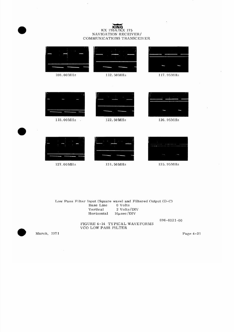
8/9/2019 KX 170A - Maintenance Manual Honeywell
http://slidepdf.com/reader/full/kx-170a-maintenance-manual-honeywell 81/586
KING
KX 170A/KX 175
NAVIGATION RECEIVER/
COMMUNICATIONS TRANSCEIVER
108. OOMHz
118. OOMHz
127. OOMHz 135.95MHz
Low Pass Filter Input (Square wave) and Filtered Output (D-C)
Base Line 0 Volts
Vertical 2 Volts/DIV
Horizontal
1Opsec /DIV
March, 197 1
696-6021-00
FIGURE 4 - 14 TYPICAL WAVEFORMS
VCO LOW PASS FILTER
Page 4-21

8/9/2019 KX 170A - Maintenance Manual Honeywell
http://slidepdf.com/reader/full/kx-170a-maintenance-manual-honeywell 82/586
KI G
7
X 170A KX 175
NAVIGATION RECEIVER /
COMMUNICATIONS TRANSCEIVER
G. VCO LOW PASS FILTER
The filter includes an elliptic low pass section to recover D-C voltage from the 25KHz
square wave and a lead-lag section to provide loop stability.
See Figure 4-14 and 4-15.
vco
LOW PASS FILTER
FIGURE 4-15 VCO LOW PASS FILTER
(Dwg. No. 696 -6022 -00)
4.2. 2.2
Circuit Theory - SMO RF Circuits
VOLTAGE CONTROLLED OSCILLATORS
The VCO is an inductively tuned, Colpitts oscillator. See Figure 4-16.
Rf, R
C
x
(b)
FIGURE 4-16 BASIC VCO PRINCIPLES
(Dwg. No.
696 -6023 -00)
(C)
Page 4-22
Rev. 2, December, 1972

8/9/2019 KX 170A - Maintenance Manual Honeywell
http://slidepdf.com/reader/full/kx-170a-maintenance-manual-honeywell 83/586
ZiK
KX 170A/KX 175
NAVIGATION RECEIVER /
COMMUNICATIONS TRANSCEIVER
A parallel tuned circuit is formed in (a) by Lbc and the series combination of Cbe and
c .
Regeneration is provided by positive feedback from the emitter to base.
ise&complished by varying the inductance of Lbc.
Tuning
tuning may be done .by varying the bias on C,.
Since w Lbc = wL1 - -1, in (b),
R1 in (c) is used as an oscillator pickoff
point. Refer to Figures 4- 17 and 4- 18 for circuitry.
+8.5VDC
w
1.
C268
1. C267
T
470
T
0. IJJf
c201
=
z
fitif
dt-
-=:
7%’
10%
R203
470
R204 ,-C206
Rev. 2, December, 1972
FIGURE 4 -17 NAV VCO
(Dwg. No.
696 -6024-00)
VHF OUT
RCVR
TUNING
VOLTAGE
TUNING
VO LTAGE
Page 4-23

8/9/2019 KX 170A - Maintenance Manual Honeywell
http://slidepdf.com/reader/full/kx-170a-maintenance-manual-honeywell 84/586
KlNG
KX l’IOA/KX 1.75
NAVIGATION RECEIVER/
COliIMUNICATIONS TRANSCEIVER
I
c302
,500
I
7‘ c307
1500
C304
I *
470
'T
T’
FSE
1
C320
“;o”,”
470
?g ;-;I;
>
.
7
w -
41
/I ”
c315
,030l
CM7
T
2-27 x .X3
HI-LO
1
_Lc3,0
svco”
vco
VHF
s 4’o
-OUT
---IL304
696-6025-00
FIGURE 4-18 COMM VCO
March, 197 1
0
age 4-24

8/9/2019 KX 170A - Maintenance Manual Honeywell
http://slidepdf.com/reader/full/kx-170a-maintenance-manual-honeywell 85/586
KING
KX 17OA/KX 175
NAVIGATION RECEIVER /
COMMUNICATIONS TRANSCEIVER
The COMM VCO is switched from the high band (127. 00 -
135. 95MHz) to the low band
(118. 00 - 126. 95MHz) by switching in trimmer capacitor C314.
The bias ground returns
(cathodes of CR301 and CR3021 are opened to disable the COMM VCO in the two unused
MHz positions.
L201, (C314) and (C315) provide an alignment adjustment for the NAV
and COMM VCO’s.
BUFFER AMPLIFIERS
The buffers are class A, broadband amplifier stages.
NAV buffer stages include Q202
and Q203. COMM buffer stages include Q303, Q304 and Q306.
The COMM transmitter
buffer stage Q306 is disabled during receive by Q305 and during SMO failure by Q307.
RECEIVER BUFFER
-l
March, 197 1
n-303 C32B
i
so IPf
I
TX. ENABLE SWITCH
FIGURE 4-19 COMM SMO BUFFER AMPLIFIERS
Page 4-25

8/9/2019 KX 170A - Maintenance Manual Honeywell
http://slidepdf.com/reader/full/kx-170a-maintenance-manual-honeywell 86/586
KX 17 ?
A7E
175
NAVIGATION RECEIVER /
COMMUNICATIONS TRANSCEIVER
IMPLICIT DIVIDE BY 2
This circuit includes a mixer and an amplifier connected as shown.
Regeneration occurs
if the gain of the amplifier is greater than the insertion loss of the mixer.
stable condition occurs when fout = 1/2in.
The only
A balanced mixer configuration is used to
provide isolation.
The amplifier is a low Q tuned amplifier.
block diagram is shown in Figure 4-20.
The implicit divide by two
F
out = F,n -Fwf
Fm= 2 f&t
FIGURE 4-20 IMPLICIT DIVIDE BY 2 DIAGRAM
(Dwg. No.
696 -6027 -00)
(YEL)
_p*
TP203I
Page 4-26
Horizontal:
1Onsec /DIV
Upper trace :
TP203
Vertical:
0: 5V/DIV
Lower trace : TP204
Vertical :
0.2V /DIV
Selected freq: 108. 65MHz
FIGURE 4-2 1 NAV IMPLICIT DIVIDE BY 2 CIRCUIT
(Dwg. No.
696 -6028 -00)
Rev. 2, December, 19’72

8/9/2019 KX 170A - Maintenance Manual Honeywell
http://slidepdf.com/reader/full/kx-170a-maintenance-manual-honeywell 87/586
KING
KX 170A/KX 175
NAVIGATION RECEIVER /
COMMUNICATIONS TRANSCEIVER
--
c355 -
I I500
lo56
9%
TOW
IO% =
e-2 AMPL.
FIGURE 4-22 COMM IMPLICIT DIVIDE BY 2 CIRCUIT
(Dwg. No.
696 -6029 -00)
REFERENCE OSCILLATOR
A Colpitts oscillator configuration is used.
The crystal forms a parallel tuned circuit
with the series combination of Cbe and C,,.
Cbe provides regenerative feedback to the
base.
I
-=
WCec
L-wL,
WC1
FIGURE 4 -23
SIMPLIFIED COLPITTS
OSCILLATOR
(Dwg. No. 696 -6030 -00)
Rev. 2, December, 1972
Page 4-27

8/9/2019 KX 170A - Maintenance Manual Honeywell
http://slidepdf.com/reader/full/kx-170a-maintenance-manual-honeywell 88/586
KI
7
X 170A KX 175
NAVIGATION RECEIVER/
COMMUNICATIONS TRANSCEIVER
The parallel combination of XC ec -XL 1 is selected to be capacitive at the desired crystal
overtone frequency and inductive at lower frequencies to suppress oscillations at the
fundamental and lower overtone frequencies.
In the COMM High Reference Oscillator the 71.025MHz crystal is selected for high SMO
band (127. 00 - 135.95MHz) and 66. 525MHz is selected for low SMO band, (118. 00-126.95-
MHz) operation.
See Table 4-2 for corresponding receive and transmit frequencies.
4
NAV HIGH REF. OSC.
b)
COMM HIGH REF. OSC.
l’age.4-28
March, 197 1
0
7
c569
0l"f
R3.6
.-..
696-6031-00
FIGURE 4-24 HIGH REFERENCE OSCILLATCHS
8/9/2019 KX 170A - Maintenance Manual Honeywell
http://slidepdf.com/reader/full/kx-170a-maintenance-manual-honeywell 89/586
KI G
7
X 170A KX 175
NAVIGATION RECEIVER /
COMMUNICATIONS TRANSCEIVER
4.3 COMM TRANSCEIVER
4.3. 1
BLOCK DIAGRAM THEORY (Figure 5-49)
The KX 170A/KX 175 COMM receiver section is a dual conversion, superheterodyne
receiver with a 9. OMHz first I-F and a 861.25KHz second I-F frequency.
360 channels
are synthesized at the first mixer.
Low side injection is used for channels 127.00 -
135. 95MHz and high side for 118. 00 - 126. 95MHz.
The received antenna signal is coupled to the preselector through a diode T/R switch.
A 2-pole, varactor tuned, R-F filter couples the antenna to the R-F stage.
A second
varactor tuned filter couples the amplified R-F signal to the 1st mixer and supplies
additional image and l/2 I-F spurious rejection.
The amplified R-F signal is mixed
with the synthesized injection frequency in a balanced mixer. A two,pole crystal filter
couples the difference frequency to the second mixer and provides image and l/2 I-F
selectivity.
The 8. 13875 MHz crystal controlled 2nd local oscillator develops injection
for the 2nd mixer. The 2nd I-F contains two integrated circuit (I-C) amplifiers with
three double-tuned interstage networks for additional receiver selectivity.
An active
detector/noise limiter provides audio gain, rate noise limiting, and 90% AM clipping of
noise spikes. A two stage AGC amplifier is used to AGC the R-F stage, and the 1st
I-C amplifier in the 2nd I-F strip.
The receiver is approximately 6db into AGC with no input signal.
This eliminates con-
ventional gain threshold effects and establishes a constant “Signal plus noise ” at the
detector output.
The detector noise bandwidth is approximately 15KHz. A noise filter
passes white noise containing frequency components above 7KHz.
The filtered noise
is amplified and used to operate a squelch gate.
When detected white noise drops below
a preset threshold, the squelch gate opens.
If a detected audio tone falls within the
filter passband, it is treated as noise and blocks the squelch.
A carrier squelch over-
comes this problem by opening the squelch gate when the AGC exceeds a predetermined
voltage.
Receiver Audio passes through the volume control, an audio amplifier and is
coupled to the audio summing junction.
The summing junction accepts four auxilary audio inputs including NAV. A diode switch
mutes the summing junction and connects the mike element to the audio power amplifier
during transmit. Headphone/sidetone is capacitively coupled from the audio drive amp-
lifier to the phone jack and is still operable with a blown fuse and shorted audio output
or R-F power transistors. The push-pull audio amplifier supplied 6 watts to the
balanced primary of the output transistor. The secondary includes separate speaker
and modulation windings.
The transmitter is a solid state, 4 stage, broadband, 30db gain, R-F power amplifier.
Collector modulation is applied to the driver and final stages. The low pass filter
March, 197 1
Page 4-29
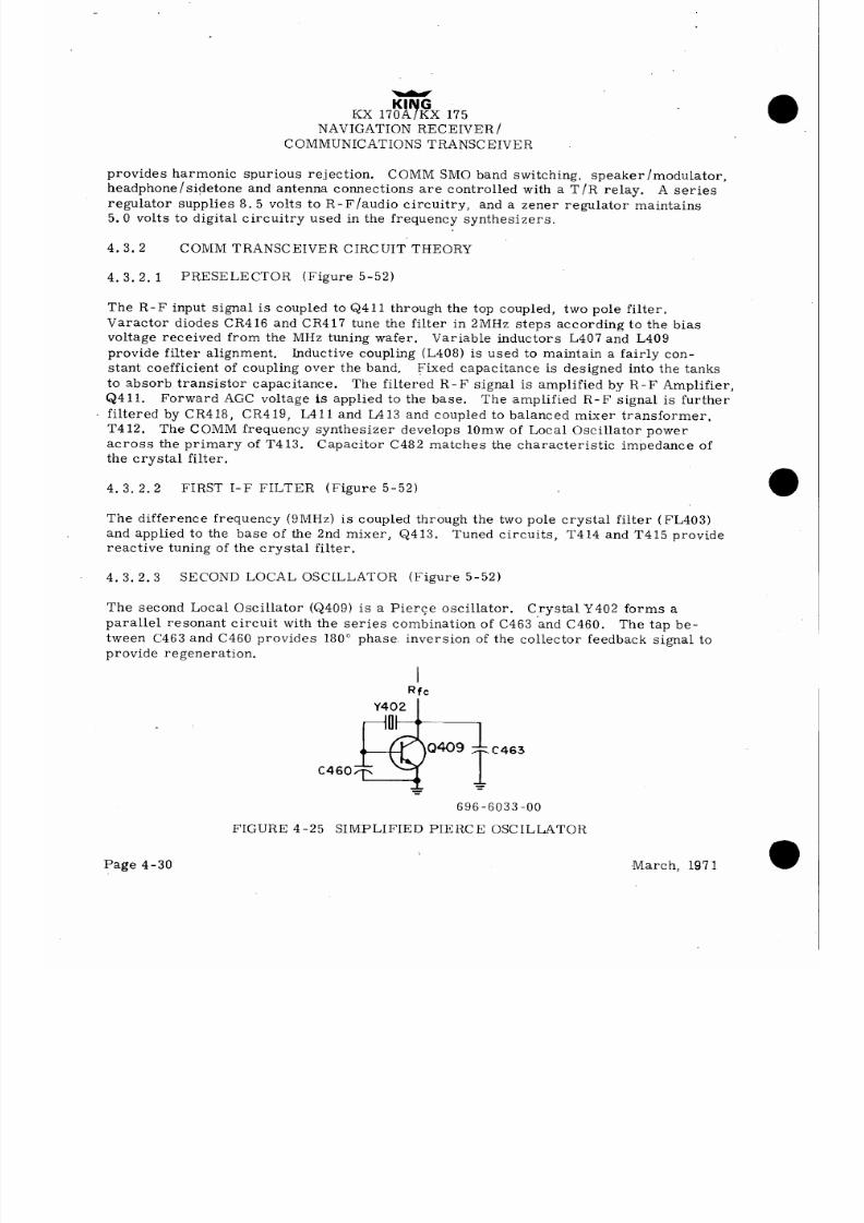
8/9/2019 KX 170A - Maintenance Manual Honeywell
http://slidepdf.com/reader/full/kx-170a-maintenance-manual-honeywell 90/586
KI G
KX 170A
7
KX 175
NAVIGATION RECEIVER /
COMMUNICATIONS TRANSCEIVER
provides harmonic spurious rejection. COMM SMO band switching, speaker/modula tor,
headphone/sidetone and antenna connections are controlled with a T/R relay. A series
regulator supplies 8. 5 volts to R-F/audio circuitry,
and a zener regulator maintains
5.0 volts to digital circuitry used in the frequency synthesizers.
4.3.2 COMM TRANSCEIVER CIRCUIT THEORY
4.3.2.1
PRESELECTOR (Figure 5-52)
The R-F input signal is coupled to Q411 through the top coupled, two pole filter.
Varactor diodes CR416 and CR417 tune the filter in 2MHz steps according to the bias
voltage received from the MHz tuning wafer. Variable inductors L407 and L409
provide filter alignment.
Inductive coupling (L408) is used to maintain a fairly con-
stant coefficient of coupling over the band. Fixed capacitance is designed into the tanks
to absorb transistor capacitance.
The filtered R-F signal is amplified by R-F Amplifier,
Q411.
Forward AGC voltage is applied to the base. The amplified R-F signal is further
filtered by CR418, CR419, L411 and LA13 and coupled to balanced mixer transformer,
T412. The COMM frequency synthesizer develops 1Omw of Local Oscillator power
across the primary of T413. Capacitor C482 matches the characteristic impedance of
the crystal filter.
4.3. 2.2
FIRST I-F FILTER (Figure 5-52)
The difference frequency (9MHz) is coupled through the two pole crystal filter (FL403)
and applied to the base of the 2nd mixer, Q413. Tuned circuits, T414 and T415 provide
reactive tuning of the crystal filter.
4.3.2.3
SECOND LOCAL OSCILLATOR (Figure 5-52)
The second Local Oscillator (Q409) is a Pierce oscillator. Crystal Y402 forms a
parallel resonant circuit with the series combination of C463 ‘and C460. The tap be-
tween C463 and C460 provides 180” phase. inversion of the collector feedback signal to
provide regeneration.
I
Rfc
C463
C460
c
696-6033-00
FIGURE 4 -25 SIMPLIFIED PIERCE OSCILLATOR
Page 4-30
.March, 197 1

8/9/2019 KX 170A - Maintenance Manual Honeywell
http://slidepdf.com/reader/full/kx-170a-maintenance-manual-honeywell 91/586
KX 17=X 175
NAVIGATION RECEIVER /
COMMUNICATIONS TRANSCEIVER
4. 3. 2.4
Second Mixer. (Figure 5-52)
The 1st I-F and the 2nd Local Oscillator signals are injected on the base of the second
mixer, Q4 13.
The difference frequency appears at the collector.
4.3.2.5
Second I-F (Figure 5-52)
The three top coupled, double tuned filters,
consisting of T416-421 and C484, C487 and
C49 1 provide receiver selectivity.
Load resistors across T416-42 1 swamp variations
in active device impedances to provide uniform band pass characteristics.
Integrated
circuits 1404 and 1405 are differential amplifiers with constant current sources, internal
biasing and decoupling resistors. See Figure 4-26.
A positive voltage applied to R474
causes a differential unbalance and AGC action in 1404.
In addition diode CR425 is
providing a variable resistance, shunt path to ground through C490. Resistor R473 is
used to minimize “deQing” of T417 with AGC action.
RI
+E
5on
T
01
R2
2.5Kn OUTPUT
3
DECCNJPLINI;
v”+
GJTPUT
0
INPUT
(TOP VIEW1
GND
0
696 -6034-00
FIGURE 4-26 SECOND I-F INTEGRATED CIRCUIT SCHEMA’I’IC
4. 3. 2.6
Detector /Noise Limiter (Figure 5-52)
CR426 and R481 develop a trickle bias for collector detection transistor, Q414.
Emit-
ter feedback resistor, R482, provides a high base impedance to minimize the loading
of T421.
Detected audio voltage gain is determined by the ratio of the effective collector
resistance and R482.
C496 establishes the collector time constant in conjunction with
the parallel collector resistance.
Noise limiter action occurs when CR427 is back biased. Detected audio is attenuated
by R489 and R490.
Resistors R488 and R492 establish a forward bias current through
CR427.
The charge storage of C498 establishes a D-C reference.
Positive noise peaks
back bias CR427 when the cathode rises to within0. 6 volts of the D-C reference.
R492 and C499 establish a time constant that restricts the rate of change of voltage at
the anode of CR427.
The rate limiting effect rounds off the leading edges of fast rise
time noise spikes. C499 couples the audio signal to the squelch gate.
March, 197 1
Page 4-31

8/9/2019 KX 170A - Maintenance Manual Honeywell
http://slidepdf.com/reader/full/kx-170a-maintenance-manual-honeywell 92/586
KI G
7
X 170A KX 175
NAVIGATION RECEIVER/
COMMUNICATIONS TRANSCEIVER
4. 3. 2. 7 AGC Amplifier (Figures 4-27, 5-52)
RF AMPL.
AGC
AGC
+a 5vDc
696-6035-00
FIGURE 4-27 COMM AGC SYSTEM
During radio turn on, the voltage at TP411 is approximately 1 volt and is established by
the R-F, and I-F bias currents flowing through R493 to ground.
R487 and C495 filter
the detector output and apply the resultant D-C to the base of Q415.
Q415 compares the
AGC threshold reference voltage generated by R484, CR432, R485, and R486 with the
filtered detector signal.
Q415 and Q416 jointly provide AGC amplification; C497 provides
additional AGC filtering.
Zener diode, CR424, provides R-F AGC delay to assure
proper receiver quieting.
Page 4-32
March, 197 1
a

8/9/2019 KX 170A - Maintenance Manual Honeywell
http://slidepdf.com/reader/full/kx-170a-maintenance-manual-honeywell 93/586
KX 17a 175
NAVIGATION RECEIVER /
COMMUNICATIONS TRANSCEIVER
4.3. 2.8 Noise AMP and Filter. (Figure 5-52)
C501, C502, C503, R500, L414 and the input impedance of Q419 form an elliptic high
pass filter that rejects frequencies below 7KHz. Q419 amplifies the noise. R504 and
RT501 provide temperature compensation. R483, the Carrier/Noise Squelch Adjust,
controls the amount of filtered noise at the tie point of R504 and RT501.
4. 3. 2. 9 Carrier to Noise Squelch Gate (Figure 5-52)
Q420 and CR429 develop 7. 5VDC across C508 when the peak to peak voltage of the white
noise,exceeds the sum of the forward voltages of the junctions of Q420 and CR429
(approximately 1.3V p-p). On positive voltage swings, Q420, charges C 508. On nega-
tive swings, CR429 clamps C507 against the new voltage on C508. Each positive noise
peak is integrated, increasing the D-C voltage across C508 untilQ420 saturates at an
emitter voltage of approximately 7. 5 volts. When the noise falls below the squelch .
threshold, R506 discharges C508 causing squelch gate diode CR431 to pass audio signals.
4. 3.2.10
Carrier Squelch. (Figure 5-52)
Q417 and Q418 form a differential amplifier for comparison of the AGC voltage with the
carrier squelch adjustment.
When the AGC voltage exceeds the reference voltage, the
collector of Q4 18 goes negative,
forward biasing squelch diode CR431.
4. 3.2. 11 Squelch Test.
(,Figure 5-52)
The test switch grounds the cathode of CR430 causing the squelch gate diode, CR431, to
pass received signals.
4.3.2. 12 Audio Preamp/Volume Control. (Figure 5-52)
Audio passes from the squelch gate to the volume control located on the front panel,
and back to class A audio amplifier, Q410.
The amplifier audio is connected to summing
junction resistor R703.
4.3.2. 13
Summing Junction T/R Diode Switch.
(-Figure 5-53)
Resistor R703-7C7 and I2722 provide a summing junction.
In the receive condition,
CR701 is reverse biased and CR702 is forward biased, passing audio to the audio pre-
driver stage, Q701. When the mike is keyed, the T / R relay grounds H721, which
mutes CR702 audio and forward biases CR701 applying mike audio to Q70l.
4. 3. 2. 14
Audio Power Amplifier. (Figure 5-53)
Transistors Q701-706 are connected in a conventional audio power amplifier configura-
tion.
Headphone sidetone is coupled from the collector of Q702 through C709.
Headphone
March, 197 1
Page 4-33

8/9/2019 KX 170A - Maintenance Manual Honeywell
http://slidepdf.com/reader/full/kx-170a-maintenance-manual-honeywell 94/586
KING
KX 170A/KX 175
NAVIGATION RECEIVER/
COMMUNICATIONS TRANSCEIVER
sidetone is obtained by connecting resistor R7 19 in series and variable resistor.R726 in
shunt with the headphone during transmit. Failure of the fuse F70 1 makes the T/R
relay (K701), the transmitter (Q601 -604) and the push-pull audio amplifier (Q703-Q706)
.inoperable.
Headphone audio remains functional.
4. 3.2. 15 Transmitter. (Figure 5-53)
The inputs to the VHF power amplifier are,
the R-F output from the buffer amplifier in
the COMM/SMO and audio from the audio modulator.
When the microphone switch is
depressed, a CW signal is coupled through C602 to the base of &SOL QSOl output from
transformer T601 is’ coupled through C605’to the base of Q602, the pre-driver amp-
lifier.
The output of &SO2 consists of the tuned circuit of T602, C609, and C610 and
couples to the base of the driver amplifier Q603,
The driver amplifier Q603, has dual emitters which are R-F by-passed by C611 and
C612.
The output tuned circuit T603, C618 and C619 drives the final amplifier. R6 13 is
used to de-Q transformer T603.
Transformer T604 and capacitor C622 match the
transmitter to the low pass filter through capacitor, C623.
RF Amplifiers Q601 and Q602 are supplied a filtered voltage from the radio D-C power
source.
The resistor and diode combination of R608, R615, CR601 and CR602 provides full
‘modulation to Q604 and upward modulation only to Q603.
c
4.2.2. 16 Low Pass Filter. (Figure 5-53)
The low pass filter is a 3 section elliptical filter made up of sections FL601, FL602,
and FL603.
Its purpose is to greatly reduce the harmonic output signals from the power
amplifier.
The filter output couples directly to the antenna jack 5172.
The resistor and diode combination used in the first two sections provide T-R switching.
In the receive condition the relay K701 supplies a positive D-C voltage to diodes CR603
and CR604 through resistors R6 16 and R617.
The capacitors C625 and C626 are VHF
bypasses, and choke L604 provides a D-C voltage return.
Received signals pass through
the 3rd filter section FL603, diode CR604, and then to the receiver.
Diode CR603 acts
to minimize the insertion loss of the T/R switch.
In the transmit condition, the D-C
voltage is removed from the resistor, diode combination by relay K701 and the R-F
power from the transmitter reverse biases diodes CR603 and CR604 due to self-
rectification.
Page 4-34
a
arch, ,197 1
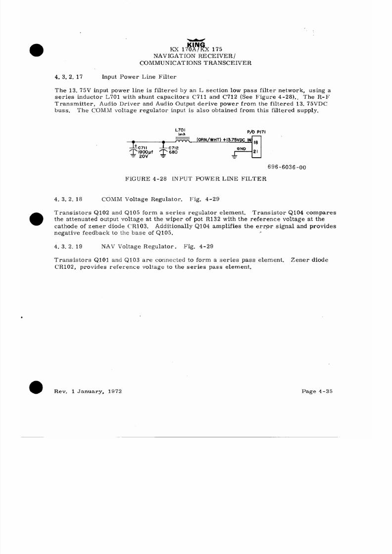
8/9/2019 KX 170A - Maintenance Manual Honeywell
http://slidepdf.com/reader/full/kx-170a-maintenance-manual-honeywell 95/586
Kx lfi%$x 175
NAVIGATION RECEIVER/
COMMUNICATIONS TRANSCEIVER
4. 3. 2. 17 Input Power Line Filter
The 13. 75V input power line is filtered by an L section low pass filter network, using a
series inductor L701 with shunt capacitors C711 and C712 (See Figure 4-28).. The R-F
Transmitter, Audio Driver and Audio Output derive power from the filtered 13. 75VDC
buss.
The COMM voltage regulator input is also obtained from this filtered supply.
L701
Imh
P/O PI71
m (ORN/WHT) ti3.75vOc IN ,8
lGND 21
=
696-6036-00
FIGURE 4-28 INPUT POWER LINE FILTER
4. 3. 2. 18 COMM Voltage Regulator. Fig. 4-29
Transistors Q102 and Q105 form a series regulator element.
Transistor Q104 compares
the attenuated output voltage at the wiper of pot R132 with the reference voltage at the
cathode of zener diode C’R103.
Additionally Q104 amplifies the err-or signal and provides
negative feedback to the base of Q105.
.-
4. 3. 2. 19 NAV Voltage Regulator. Fig. 4-29
Transistors QlOl and Q103 are connected to form a series pass element.
Zener diode
CR102, provides reference voltage to the series pass element.
Rev. 1 January, 1972
Page 4-35

8/9/2019 KX 170A - Maintenance Manual Honeywell
http://slidepdf.com/reader/full/kx-170a-maintenance-manual-honeywell 96/586
iE
7
X 170A
KX 175
NAVIGATION RECEIVER /
COMMUNICATIONS TRANSCEIVER
RI27
75
5%
_ NW +13.75VDC
YELIWHT
FROM NAV FILTER
t 13.75vDC
TO NAi’ REC., NAV SMO,
905 FOR G.S. SWITCHING. ‘.
_.
TO ‘AUDIO BOARD AND
NAV SMO 400 K C. OSC
FROM C@,jM. FILTER
+ I3.75Vw.z
l
TO COMM. REC., COMM. SMO,
REG. OUTPUT SlO2 TUNING VOLT.
Rl3;
FIGURE 4-29 REGULATOR SCHEMATICS
Page 4-36
March, 197 1
a
8/9/2019 KX 170A - Maintenance Manual Honeywell
http://slidepdf.com/reader/full/kx-170a-maintenance-manual-honeywell 97/586
KI
Y
X 170A KX 175
NAVIGATION RECEIVER /
COMMUNICATIONS TRANSCEIVER
4.4 NAV RECEIVER
4.4. 1
BLOCK DIAGRAM THEORY (Figure 5-48)
The KX 170A/KX 175 NAV receiver section is a dual conversion, superheterodyne
receiver with a 15. 1875MHz first I-F and a 1. 1857MHz second I-F frequency. The 200
channels are synthesized at the first mixer and low side injection is used for all channels.
A 2 pole, varactor tuned, R-F filter couples the antenna to the R-F stage .
A single
pole, varnctor tuned filter, couples the amplified R-F signal to the 1st mixer and
supplies additional image and l/2 I-F spurious rejection.
The amplified R-I;’ signal is
mixed with the synthesized injection frequency in a balanced mixer.
-4 crystal i‘ilter couples the difference frequency to the second mixer and provides
i -na ,re :Ind l/2 1-F selectivity. The 14. 0018MHz, crystal controlled, 2nd Ldcal Oscil-
lator develop::- in,lection for the 2nd mixer. ,
The 2nd I-F contains two I-C amplifiers
l:iriti-1 ttlr,c:e double tuned interstage networks for receiver selectivity.
An active detector
pr:)i,~iiies audio gain.
An emitter follower couples the detector signal to the noise limit-
er and the ,4GC amplifier. The noise limiter clips noise peaks corresponding to greater
than 90% AM modulation and provides rate limiting.
A two stage, AGC amplifier is used
to AGC the R-F stage, and the 2nd I-F strip.
The receiver is approximately 6db into AGC with no input signal. This eliminates con.-
ventional receiver gain threshold effects.
The audio signal from the rate noise limiter
prisses through a panel switch controlled 1020Hz ident filter,
the volume control and
til,Jn to an I-C audio amplifier providing a 50mw 600 ohm output.
The 1’: - f? input
signal is coupled to the R-E’ amplifier Q401, through a capacitor coupled
l;vo pole filter.
Variable inductors,
L40 1 and L403 provide filter alignment.
Varactor
diodes Cl%401 and CR402 tune the filter continuously according to the b,ias voltage
receiyvred from the NAV VCO. The filtered Ii- II‘ signal is amplified by f<- I;‘ amplifier,
Q401,
and gain is controlled by applying forward ACIC voltage to the base.
i.-he amp-
lified Z-I;‘ signal is filtered by I.,405 and Ctt403,
tuned by the bias voltage from the
N:\\,’ ,SWtO, <and coupled to the balanced mixer transformer, ‘1‘401.
The NAL’ frequency
synthesizer develops 10mw of Local Oscillator power across the primary of mixer
transformer l-402.
bllarch, 197 1
Page 4-37

8/9/2019 KX 170A - Maintenance Manual Honeywell
http://slidepdf.com/reader/full/kx-170a-maintenance-manual-honeywell 98/586
. .
.:
KX 17t
A”) ?
x 175
NAVIGATION RECEIVER/
COMMUNICATIONS TRANSCEIVER
4.4.2.2’ First I-F Filter (Figure 5-52)
The difference frequency 15. 1875MHz generated by the balanced mixer, CR404-407,.
T401, and T402 is matched to the crystal filter through C415.
The crystal filter output
is capacitively coupled (C417) to the base of the second mixer Q403.
4.4.2.3 Second Local Oscillator (Q408) is a Pierce oscillator. (Figure 5-52)
Crystal Y401 forms a parallel resonant circuit with the series combination of C448 and
C447. The tap be$ween C448 and C447 provides 180” phase inversion of the collector
feedback signal to provide regeneration. (See Figure 4-27)
4.4. 2.4
Second Mixer (Figure 5-52)
The 1st I. F. and the 2nd Local Oscillator signals are injected on the base of the second
mixer, Q403.
The difference frequency appears at the collector.
4.4. 2. 5 Second I. F.
( Figure 5-52)
The three capacitor coupled, double tuned filters consisting of T405 - 410 and C419,
C424 and C428 provide receiver selectivity.
Load resistors across T405- 4 19
swamp variations in active device impedances to provide uniform band pass character-
istic s. Integrated circuits 1401 and 1402 are differential amplifiers with a constant
current source, internal biasing and a decoupling resistor.
See Figure 4-28. A
positive voltage applied to R4 14 causes a differential unbalance and AGC action in 140 1.
In addition diode CR409 is forward biased, providing an AGC’d shunt path to ground
tllrough C422.
Resistor R413 is used to minimize
“de Q ing” of T406 with AGC action.
4. 4. 2. 6
DETECTOR/NOISE LIMITER. (Figure 5-52)
CR4lOand It421 developa trickle bias for collector detection transis tor, Q404. Emitter
feedback resistor,
R424, provides a high base impedance to minimize loading of T410.
Voltage gain of the detected audio is determined by the ratio of the effective collector
resistance and R424.
C437 establishes the collector time constant in conjunction with
the parallel collector resistance.
Emitter follower, Q405, serves to minimize the
loadhg effect of the noise limiter on the detector
(Q404)
output.
Noise Limiter action occurs when CR411 is reverse biased. Detected audio is attenuated
by R428 and R427.
Resistors R429 and R430, and diode CR412, establish a bias current
through CR41 1.
The charge storage of C440 establishes a DC reference.
Positive noise
peaks
back
bias CR411 when the cathode rises to within 0. 6 volts of the DC reference.
12429, <:439 and C438 establish a time constant that restricts the rate of change of volt-
age at the anode of CR4 11.
The rate limiting effect rounds off the, corners of fast rise
time noise spikes.
C439 couples the audio signal to the ident filter.
Page 4-38
March, 197 1

8/9/2019 KX 170A - Maintenance Manual Honeywell
http://slidepdf.com/reader/full/kx-170a-maintenance-manual-honeywell 99/586
KING
KX 170A/KX 175
NAVIGATION RECEIVER/
COMMUNICATIONS TRANSCEIVER
4.4, 2. 7 VOR/LOC OUTPUT (Figure 5-52)
The VOR/LOC signal is available at the collector of detection transistor Q404.
R425
is provided to set the VOR/LOC output level that is coupled through C443 to the rear
connector of the KX 170A/KX 175.
4.4. 2. 8 AGC AMPLIFIER (Figures 5-52, 4-30)
During radio turn on, the voltage at TP406 is approximately 1 volt and is established
by the R-F, and I-F bias currents flowing through R437 to ground.
R431 and R432 with
C444 and C441 filters the detector output and applies the resultant D-C to the base of
Q406. Q406 compares the AGC threshold reference voltage at the junction of RT502
and R434 with the filtered detector signal.
Q406 and Q407 jointly provide AGC amplification.
C442 provides additional filtering,
A trade off is made between AGC response time and AGC line filtering of the 30Hz
component of the detector signal.
The AGC amplifier/filter network shifts the 30Hz
residue 180” from the detected 30Hz, which minimizes phase distortion of the 30Hz AM
component of the VOR signal.
Zener diode CR408 initially conducts in the forward direction applying full AGC to the
I-F. As signal level increases, CR408 is biased off applying full AGC to the RF stage.
A further increase of the RF signal causes the diode to conduct in the reverse direction
applying AGC to both the R-F and I-F stages.
+B SVDC
T
T
RF AMPL.
9
AGC
TP40f
AGC
I
7
I A6c
I
t6.5VDC
FIGURE 4-30 NAV AGC SYSTEM
March, 197 1
Page 4-39

8/9/2019 KX 170A - Maintenance Manual Honeywell
http://slidepdf.com/reader/full/kx-170a-maintenance-manual-honeywell 100/586
3iz
KX 170A/KX 175
NAVIGATION RECEIVER/
COMMUNICATIONS TRANSCEIVER
4. 4. 2. 9
IDENT FILTER/VOLUME CONTROL. (Figure 5-52)
C439 cou$es the audio signal to the Ident Filter. The 1020 Hz tone filter L703 and C716
are switched in or out by the front panel Ident Switch.
The audio signal passes from the
Ident Filter to the volume control on the front panel and back to the I-C audio amplifier
1403. Components R448, R449, L406 and C454-C457, form an elliptic low pass filter
providing a sharp frequency rolloff above 3KHz.
R450 and C458 develop negative feed-
back to stabilize gain and minimize broadband output noise.
Transformer T411 trans-
forms the output impedance of audio amplifier 1403 to 500 ohms and this audio output is
provided at the rear connector of the KX 170A/ KX 175.
The voltage supply for 1403 is
stabilized by zener diode CR414 and filtered by C452.
4.5 KA 39 VOLTAGE ONVERTER (Figure 5 -56)
The KA 39 consists of dual series regulators,
converting 27. 5VDC to 13. 75VDC. The
“A”
regulator provides COMM excitation,
while the “B” regulator provides NAV
excitation.
Zener diodes CR101 and CR104 provide reference voltages to the darlington
series pass elements QlO2 - QlOl and Q104 - Q103 respectively.
Diodes CR102 and
CR103 offer transient and reverse power application protection.
INPUT
--
--
RI04
6n
1’
0
I
I
I
O,,PUT
I-
&
KA-39 CONVERTER
mm-
--
-I
002-Ol62-OO(R-2)
FIGURE 4-31 KA39 VOLTAGE CONVERTER SCHEMATIC DIAGRAM
Page 4-40
March, 197 1

8/9/2019 KX 170A - Maintenance Manual Honeywell
http://slidepdf.com/reader/full/kx-170a-maintenance-manual-honeywell 101/586
KI G
7
X 170A KX 175
NAVIGATION RECEIVER/
COMMUNICATIONS TRANSCEIVER
SECTION
MAINTENANCE
5.1 TESTEQUIPMENT
i
The following test equipment, or equivalent,
is required to properly align and test the
KX 170A/KX 175 system. All test equipment must be properly calibrated before align-
ment and tests are started.
a.
b.
C.
d.
e.
f.
g.
h.
1.
j.
k.
1.
m.
n.
Major Power Supply: Electra Model NFB (Filtered)
Auxilary Power Supply: H eath Model IP-20
Digital Voltmeter: Eldorado 1820A
VTVM: Heath Model IM-13
Audio Wattmeter With Load: Eico Model 261
VHF Wattmeter With 5Oa Load: Bird Termaline Model 6 11
Frequency Counter: ELDORAD O Model 1615 with option C.
VHF Signal Generator: Boonton Model 211A
HF Signal Generator: Hewlett Packa rd Model 606A
Audio Oscillator: Hewlett Packard Model 200CD
2
VOR/LOC Signal Generator: Collins Model 479S-3
Oscilloscope: (30MHz Dual Trace Minimum) Tektronix Model 454
Recommended
VHF AM Detector: (See Figure 5-9)
KX 170A/KX 175 Bench Test Set (See Figure 5- 11)
Rev. 2, December, 1972
Page 5-l

8/9/2019 KX 170A - Maintenance Manual Honeywell
http://slidepdf.com/reader/full/kx-170a-maintenance-manual-honeywell 102/586
KING
KING
KX 170A/KX 17’5
NAVIGATION RECEIVER/
COMMUNICATIONS TRANSCEIVER
5.2 ALIGNMENTNDTESTPROCEDURE
5.2. 1 NAV SMO ALIGNMENT AND TEST (Figures 5-1, 5-3)
696
-6040 -00
FIGURE 5-1 NAV SMO TEST POINT AND ALIGNMENT LOCATIONS
Page 5-2
a.
Remove the dust covers.
b.
Remove three screws on each side of the COMM SMO tray and one screw
at the front. Pivot the COMM SMO up and over the front of the radio.
C. Remove two screws in center area of NAV SMO cover and remove cover.
d. Connect a digital voltmeter to CR214 (5. 1V Zener Diode)
e.
Apply 13. 75 volts to NAV Receiver (switch power on NAV only) and observe
voltage at C R2 14, if greater than 5. 75 volts, switch power off to avoid I. C.
damage.
If OK proceed to next step.
f.
Connect a digital voltmeter to the anode lead of, CR101 at NAV Voltage
Regulator and observe an 8. 5 f. 5 volts indication on voltmeter .
g*
NAV Receiver power requirements are 13. 75 volts input at .45 amp with no
modulated RF signal present.
h.
Set the NAV frequency selector to 117. 95OMHz.
1.
Connect a digital voltmeter to TP 20 1 and adjust L201 for 7. 200 -VDC tuning
(VCO) voltage.
j.
Do not attempt field alignment of the 25KHz filter T201.
k.
(Optional) NAV SMO frequency stability and tuning (VCO) voltage m ay be
observed simultaneously by connecting a frequency counter to the coax
side of C231 10 pf disc capacitor) and connecting a digital voltmeter to
the tuning voltage line (red wire at C2 58 feed thru c apacitor).
Rev. 4, January, 1.976

8/9/2019 KX 170A - Maintenance Manual Honeywell
http://slidepdf.com/reader/full/kx-170a-maintenance-manual-honeywell 103/586
KING
KX 170A/KX 175
NAVIGATION RECEIVER
COMMUNICATIONS TRANSCEIVER
Channel the NAV frequency selector through the followmg frequencies, com-
paring the frequency and tuning (VCO) voltage with Table 5-l.
Channel SMO Frequency
Tuning (VCO) Voltage
Typica.
108. 00 92.8 125 MHz
109.00
93.8 125 MHz
110.00
94.8 125 MHz
111.00 95.8 125 MHz
112.00 96. 8 125 MTIz
113.00 97.8 125 MHz
114. 00 98.8 125 MHz
115.00
99.8 125 MHz
116. 00 100. 8 125 MHz
117.00 101.8125 MHz
117.95
102.7625 MHz
2.84 VDC
3. 15 VDC
3.49 VDC
3. 85 VDC
4. 24 VDC
4.66 VDC
5. 11 VDC
5. 59 VDC
6. 10 VDC
6. 66 VDC
7. 20 VDC
TABLE 5-l NAV CHANNEL-SMO FREQUENCY -VCO TUNING VOLTAGE
1.
Replace NAV SMO cover and install the two screws previously removed.
Rev. 2, December, 1972
Page 5-3

8/9/2019 KX 170A - Maintenance Manual Honeywell
http://slidepdf.com/reader/full/kx-170a-maintenance-manual-honeywell 104/586
KING
- T307
- TP301
- TP302
-cc315
-c314
/
TP303
696-6041-00
5-2 COMM SMO TEST POINT AND ALIGNMENT LOCATIONS
KING
KX 17OA/KX 175
NAVIGATION RECEIVER/
COMMUNICATIONS TRANSCEIVER
5. 2. 2 COMM SMO ALIGNMENT AND TEST (Figures 5-2, 5-3)
a.
Remove the two screws and top cover from the COMM SMO.
b.
Temporarily remount COMM SMO with a screw in center at each side.
C.
Connect a digital voltmeter at CR319 (5. 1V zener diode)
d. Apply 13. 75 volts to COMM Receiver (switch power on COMM only) and
observe voltage at CR319, if greater than 5. 75 volts, switch power off to
avoid I. C. dama ge.
If OK proceed to next step.
e. Connect a digital voitmeter to the anode lead of CR104 at COMM Voltage
Regulator and adjust R 132 for 8. 500 VDC.
f. Recheck voltage at CR319 for 5. 1 f . 5V, if out of tolerance switch power
off and check.
z*
COMM Receiver power requirements are 13. 75 volts input at . 65. amp with
no modulated RF signal present.
h. Connect a digital voltmeter to TP301.
1.
Set the COMM frequency selector to 126. 95MHz and adjust C315 for 7.00
VDC VCO tuning voltage at TP301.
j.
Set the COMM frequency selector to 135. 95MHz and adjust C3 14 for 7.00
VDC VCO tuning voltage at TP30 1.
k.
Recheck previous adjustments “i” and “j”.
1.
Do not attempt field alignment of the 25KHz Filter T307.
m. (Optional) COMM SMO frequency stability and VCO voltage may be observ-
ed simultaneously by connecting a frequency counter to TP303 and connect-
ing a digital voltmeter to TP301.
Page 5-4
Rev. 2, December, 1972

8/9/2019 KX 170A - Maintenance Manual Honeywell
http://slidepdf.com/reader/full/kx-170a-maintenance-manual-honeywell 105/586
KING
KX 170A/KX 175
NAVIGATION RECEIVER/
COMMUNICATIONS TRANSCEIVER
Channel the COMM frequency selector through the following frequencies,
comparing the frequency and VCO voltage with Table 5-2.
Channel
118. 00
127.00 MHz
119.00
128.00 MHz
120.00 129.00 MHz
121.00
130.00 MHz
122.00 131.00 MHz
123.06 132.00 MHz
124.00 133.00 MHz
125.00
134.00 MHz
126.00 135.00 MHz
126. 95 135.95 MHz
127.00 118.00 MHz
128.00 119.00 MHz
129.00
120.00 MHz
130.00 121.00 MH
13 1.00
122.00 MHz
132.00
123.00 MHz
133.00
124.00 MHz
134.00 125.00 MHz
135.00 126.00 MHz
135.95
126.95 MHz
Receive SMO Frequency
VCO Voltage
Typical
2. 58 VDC
2.93 VDC
3. 30 VDC
3.. 7 1 VDC
4. 16 VDC
4.66 VDC
5. 18 VDC
5.77 VDC
6. 38 VDC
7. 00 VDC
2. 58 VDC
2.93 VDC
3. 30 VDC
3.71 VDC
4. 16 VDC
4. 66 VDC
5. 18 VDC
5.77 VDC
6. 38 VDC
7.00 VDC
TABLE 5-2 COMM CHANNEL-RECEIVE SMO FREQUENCY -
VCO TUNING VOLTAGE
n. Remove the temporary mounting screws and position COMM SMO cover in
place with the two screws previously removed.
0. Mount the COMM SMO tray with three screws on each side and one screw
at the fron t.
Rev.
2,
December, 1972
+8.5VDC NAV -
CRlOl-----
+8vDcy
CR104
+8.5VDC COMM
R132
KING
NAV
-VOLTAGE
REGULATO
COMM
- VOLTAGE
REGULATO
696-6042-00
FIGURE 5-3 NAV AND COMM VOLTAGE REGULATORS
Page 5-5

8/9/2019 KX 170A - Maintenance Manual Honeywell
http://slidepdf.com/reader/full/kx-170a-maintenance-manual-honeywell 106/586
KING
NAV VCO
, TUNING
ADJUSTMENT
5-4 NAV VCO TUNING ADJUSTMENT LOCATION
Page 5-6
KING
KX 170A/KX 175
NAVIGATION RECEIVER/
COMMUNICATIONS TRANSCEIVER
5. 2. 3 NAv/C0MM RECEIVER PRELIMINARY ALIGNMENT TE::T
a.
Remove the receiver board retaining screws (5 places) noting the positiolt
of the ground lug. Loosen the two hinge pivot screws, pivot the board 90
and retighten the hinge pivot screws.
b.
Set channel selector to 117. 95 MHz and connect a digital voltmeter to the
NAV receiver tuning voltage test point (TP40 1 of Figure 5-6B) and ohs:. rve
7.20 VDC.
If correct verify the tuning voltage versus channel frequency
of Table 523.
If not 7.20 VDC. L201 may be adjusted through access
hole in bottom of NAV SMO tray’ (Figure 5-4). Refer to 5. 2. 1 for adjust-
ment procedure.
C.
Connect a frequency counter to point “X” o f Figure 5-6A and verify the
SMO frequency versus channel frequency of Table 5-3.
’
Channel
108.00 92.8 125 MHz
109.00
93.8 125 MHz
110.00 94.8 125 MHz
111.00 95.8 125 MHz
112.00 96.8 125 MHz
113.00 97.8 125 MHz
114.00 98.8 125 MHz
115.00 99.8125 MHz
116.00 100.8 125 MHz
117.00 10 1.8 125 MHz
117.95
102.7625 MHz
SMO Frequency Receiver Tuning
Voltage Typical
2.84 VDC
3. 15 VDC
3.‘49 VDC
3.85 VDC
4. 24 VDC
4. 66 VDC
5. 11 VDC
5. 59 VDC
6. 10 VDC
6. 66 VDC
7. 20 VDC
TABLE 5-3 NAV CHANNEL-SMO FREQUENCY -
RECEIVER TUNING VOLTAGE
March, 197 1

8/9/2019 KX 170A - Maintenance Manual Honeywell
http://slidepdf.com/reader/full/kx-170a-maintenance-manual-honeywell 107/586
KING
KX 170A/KX 175
NAVIGATION’ RECEIVER/
COMMUNICATIONS TRANSCEIVER
d.
Connect a digital voltmeter to the COMM receiver tuning volt age test point
(TP408 of Figure 5-6B) and verify the tuning voltage versus channel fre-
quency of Table 5-4.
e.
Connect a frequency counter to point
“Y” of Figure 5-6A and verify the
SMO frequency versus channel frequency of Table 5-4.
Channel
118.00
127.00 MHz
119.00 128. 00 MHz
120.00
129.00 MHz
121.00
130.00 MHz
122.00 131.00 MHz
123.00
132.00 MHz
124.00 133.00 MHz
125.00
134.00 MHz
126.00,
135.00 MHz
126. 95
135.95 MHz
127.00
118.00 MHz
128.00
119.00 MHz
129.00
120.00 MHz
130.00
121.00 MHz
131.00
122.00 MHz
132. 00
123.00 MHz
133.00
124.00 MHz
134.00
125.00 MHz
13 5. 00
126.00 MHz
135.95
126.95 MHz
SMO Frequency Tuning Voltage
Typic al
2.94 VDC
2.94 VDC
3. 34 VDC
3. 34 VDC
3.80 VDC
3.80 VDC
4.31 VDC
4.31 VDC
4. 87 VDC
4.87 VDC
4.87 VDC
5. 50 VDC
5. 50 VDC
6. 20 VDC
6. 20 VDC
6.99 VDC
6.99 VDC
7.86 VDC
7.86 VDC
7.86 VDC
TABLE 5-4 COMM CHANNEL-RECEIVE SMO FREQUENCY -
TUNING VOLTAGE
March, 197 1
Page 5-7

8/9/2019 KX 170A - Maintenance Manual Honeywell
http://slidepdf.com/reader/full/kx-170a-maintenance-manual-honeywell 108/586
KING
- L703
6044 -
00
NAV IDENT FILTER ADJUSTMENT LOCATION
KING
KX 170A/KX 175
NAVIGATION RECEIVER /
COMMUNICATIONS TRANSCEIVER
5. 2.4
NAV RECEIVER ALIGNMENT (KX 170A/KX 175)
5. 2.4. 1
a.
b.
C.
d.
e.
5. 2.4. 2
a.
b.
-NOTE-
DO NOT attempt to align the NAV Receiver without
firstreading the alignment procedure in full.
PRELIMINARY PROCEDURE
Test points and alignment references may be located on Figures 5-5, 5-6A
and 5-6B.
Apply 13. 75 VDC to unit and place the NAV “OFF-VOICE-IDENT” switch
in the “IDENT” position.
Set the NAV frequency selector to 108. OOMHz.
Connect a digital voltmeter to TP406 (NAV AGC test point).
Set the RF signal generator output for 10~~ hard at a frequency of 108. 00
MHz (use frequency counter) and connect to NAV antenna input connector.
ALIGNMENT PROCEDURE
Preliminary - If receiver is badly out of alignment, peak all tuning adju st-
ments (2nd IF, 1st IF and RF).
Loading and tuning is necessary to obtain desired bandpass characteristics.
5. 2.4.
3 2nd
I. F. ALIGNMENT
a.
Load point N (T409) with 3. 3KR and peak (T 4 10)
b.
Load point M (T410) with 3. 3Ka and peak (T409)
C.
Load point P (T407) with 3. 3KR and peak (T4 08)
d.
Load point 0 (T408) with 3. 3Kn and peak (T407)
e.
Load point R (T40 5) with 3. 3Kn and peak (T 406)
f.
Load point Q (T406) with 3. 3KR and peak (TA O5)
Page 5-8
Rev. 1 January, 1972
8/9/2019 KX 170A - Maintenance Manual Honeywell
http://slidepdf.com/reader/full/kx-170a-maintenance-manual-honeywell 109/586
KX 17 ?? % 175
NAVIGATION RECEIVER/
COMMUNICATIONS TRANSCEIVER
5. 2. 4.4 1st I. F. ALIGNMENT (KX 170A Only)
a.
Load point T (T403) to ground with 3. 3K and peak (T404).
b.
Load point S (T404) to ground with 3. 3K and peak (T403).
1st I. F. ALIGNMENT (KX 175 Only)
Repetitively peak (T403) and (T404) until no further improvement.
(No
load used)
5. 2.4.5
PRESELECTOR ALIGNMENT
a. Load point W (L40 1) to ground with 220R and repetitively peak (L403)
and (L405) until no further improvement.
b.
Load point V (L403) to ground with 2200 and peak (L40 1).
5.2.4.6 AUDIO FILTER L406 ADJUSTMENT
a.
RF input, 30% externally modulated with 6.48KHz audio signal. (Use
frequency counter).
b.
Adjust L406 for minimum audio output.
5. 2.4.7
IDENT FILTER L703 ADJUSTMENT (See Figure 5-5)
a.
Set the NAV “OFF-VOICE-IDENT” switch in the “VOICE” position.
RF
input, 30% externally modulated with 1020Hz audio signal. (Use fre-
quenc y counter).
b.
Adjust L703 for minimum audio output.
5. 2.4.8 VOR/LOC OUTPUT LEVEL ADJUSTMENT R425 (See Notes)
a.
Modulate the VHF generator with a Standard LOC Modulation Signal
from the VOR/ LOC generator.
b. Connect an RMS A-C voltmeter at TP407 (VOR/LOC output),
C.
VOR/ LOC output must be loaded with a KI 20 1C or KI 2llC Indicator
d. Adjust R425 for 0. 35 volt RMS LOC output at TP407 (VOR/LGC output).
March, 197 1
Page 5-9

8/9/2019 KX 170A - Maintenance Manual Honeywell
http://slidepdf.com/reader/full/kx-170a-maintenance-manual-honeywell 110/586
KING
KX 170A/KX 175
NAVIGATION RECEIVER/
.:
COMMUNICATIONS TRANSCEIVER
5. 2. 5
COMM RECEIVER ALIGNMENT (KX 170A/KX 175)
-NOTE-
Do Not attempt to align the COMM Receiver without
first reading the alignment proce.dure in full Do Not
depress the mike button ‘when signal generator is
connected to the antenna connector
5. 2. 51 1
,
PRELIMINARY PROCEDURE
a.
Test points-and alignment references may be located on Figures 5-6A
and 5-6B.
b.
Apply 13. 75 VDC to unit and place the “OFF-ON-TEST” switch in the
“TEST” position (squelch open).
.
C.
Set the COMM frequency selector to 127. 00 MHz.
d. Connect a digital voltmeter to TP411 (COMM AGC test point).
e. Set the RF signal generator output for 20 pv hard at a frequency of
127. OOMHz (use frequency counter) and connect to COMM antenna input
connector,
5. 2. 5. 2
ALIGNMENT PROCEDUKE ’
a
.
Preliminary-If receiver is badly out of alignment, peak all tuning adjust-
ments (2nd IF, 1st IF and RF).
b.
Loading and tuning is necessary to obtain desired bandpass characteristics.
5. 2. 5. 3 2nd I. F. ALIGNMENT
a.
Load point B (T420) with 3. 3 tin and peak (T42 1).
b.
Load point A (T42 1) with 3. 3KR and peak (T420).
C.
Load point D (T418) with 3. 3KSl and peak (T419).
d. Load point C (T4 19) with 3. 3K0 and peak (T4 18).
e.
Load point F (T416) with 3. 3Kf2 and peak (T4 17).
f. Load point E (T417) with 3. 3 KR and peak (T4 16).
Page 5- 10
March, 1971 .
a

8/9/2019 KX 170A - Maintenance Manual Honeywell
http://slidepdf.com/reader/full/kx-170a-maintenance-manual-honeywell 111/586

8/9/2019 KX 170A - Maintenance Manual Honeywell
http://slidepdf.com/reader/full/kx-170a-maintenance-manual-honeywell 112/586

8/9/2019 KX 170A - Maintenance Manual Honeywell
http://slidepdf.com/reader/full/kx-170a-maintenance-manual-honeywell 113/586

8/9/2019 KX 170A - Maintenance Manual Honeywell
http://slidepdf.com/reader/full/kx-170a-maintenance-manual-honeywell 114/586

8/9/2019 KX 170A - Maintenance Manual Honeywell
http://slidepdf.com/reader/full/kx-170a-maintenance-manual-honeywell 115/586
KING
KX 170A/KX 175
NAVIGATION RECEIVER/
COMMUNICATIONS TRANSCEIVER
----vm
BNC
4.7K
INPUT
MINIMUM. STRAY
CAPACITANCE 1
I
I. ALL LEADS SHOULD BE SHORT AS POSSIBLE.
2. DETECTOR SHOULD BE HOUSED IN SMALLSHIELDED
MINIBOX.
3. ALL RESISTORS ARE 1/4W,5% CARBON.
696-6049-00
FIGURE 5-9 DETECTOR SCHEMATIC DIAGRAM
ATTENUATED
RF OUTPUT
696-6050-00
FIGURE 5-10 RF ATTENUATOR SCHEMATIC DIAGRAM
March, 197 1 Page 5-15

8/9/2019 KX 170A - Maintenance Manual Honeywell
http://slidepdf.com/reader/full/kx-170a-maintenance-manual-honeywell 116/586
KING
r
--
1
42PIN AMPHENOL
5171
(NAV)
1
20
33
21
38
17
18
3
36
35
41
34
LtO
39
NAV. +13.75VDC
I
POWER INPUT
LAMP DIM'R.
1
+ +13,75VDC
POWER GND.
LAMP DIM'R. GND.
1
c GROUND
z
r----i
COMM. SWITCHED BUSS
COMM. +13.75VDC
VORiLOC OUTPUT
AUX. AUDIO #l IN
NAV. SOOAOUT
SPKR. hAOUT
SPKR. GND.
COMM. 500 OUT
--I
=
SPKR.
T
COPPI. PHONE
MIKE KEY
x-
MIKE AUDIO
xl
MIKE
TRANSMITTER
”
L
-I
FIGURE 5-11 KX 170-A/KX 175 BENCH TEST SETUP
696-6051-00
Page 5-16
March, 197 1
a

8/9/2019 KX 170A - Maintenance Manual Honeywell
http://slidepdf.com/reader/full/kx-170a-maintenance-manual-honeywell 117/586
KING
KX 170A/KX 175
NAVIGATION RECEIVER/
COMMUNICATIONS TRANSCEIVER
5. 2. 8 KX 17OA/KX 175 & Test Data
(Refer to the Installation Manual for Technical Characteristics)
COMMUNICATIONS TRANSCEIVER
Serial No.
Date
Preliminary Visual Inspection:
a.
Hardware:
(ok)
Input Voltage :
VDC
1.
Receiver Sensitivity:
b.
Paperwork
(.ok)
a.
s+n/n: 118. OOMHz db
119.95MHz db
126.70MHz db
134. OOMHz
135.95MHz
db
db
b.
Quieting:
db (frequency = 126. 7)
2.
AGC Characteristics:
db (frequency = 126. 7)
3. Selectivity:
a.
6db Bandwidth: 126. 70MHz: Above
KHz Below
KHz
62.
5db Bandwidth: 126. 70MHz: AGC reference voltage
VDC
126. 75MHz: db 126.65MHz
db
4.
Manual Gain Control:
mw max. watts min.
Transmitter Frequency Stability:
118.00
KHz
125.35
KE3Z 131.70
KHz
118. 05 KHz 125. 40 KHz 132.75 KHz
119. 10 KHz 126.45 KHz 133.80 KHz
120. 15 KHz 127. 50 KHz 134.85 KHz
12 1.20 KHz 128. 55 KHz 135.90 KHz
122. 25 KHz 129. 60 KHz 135.95 KHz
123. 30 KHz 130. 65
KHz
Rev. 4, January, 1976
Page 5-17
8/9/2019 KX 170A - Maintenance Manual Honeywell
http://slidepdf.com/reader/full/kx-170a-maintenance-manual-honeywell 118/586
KX 17 $ % 175
NAVIGATION RECEIVER/
COMMUNICATIONS TRANSCEIVER
5.
Headphone Audio : mw
6.
Squelch: a.
Carrier/Noise Squelch set for
PV
b.
Carrier /Squelch set for
YV
C.
Squelch Test
(ok)
7.
Aux. Audio: # 1
watts min.
#2
#3
watts min.
watts min.
#4
watts min.
Transmitter:
1. Power Out:
118. OOMHz
watts 126.45MHz
watts 135. 9OMHz
watts
Low Voltage :
118. OOMHz
watts
126.45MHz
watts
135. 9OMHz watts
2.
Modulation:
Capabilities
a.
Microphone : Input
VRMS
b. 118. OOMHz 126. 50MHz
127. 5OMHz
135. 95MHz
C.
Sidetone :
mw min.
mw max.
(2. 2.7)
mw final adjust
Hardware
ok
Paperwork
Glyptol
Test Stamp
ok
ok
ok
3.
Transmitter Frequency Stability:
118.00 KHz
124.35
KHz 131. 70 KHz
118. 05
KHz
125.40
KHz
132.75 KHz
119. 10
KHz 126.45 KHz
133.80 KHz
120. 15
KHz 127.50 KHz
134.85 KHz
121.20
KHz 128:55 KHz
135.90 KHz
122. 25
KHz 129. 60 KHz
135.95
KHz
123. 30
KHz 130. 65 KHz
Page 5-18
Rev. 4, January, 1976;

8/9/2019 KX 170A - Maintenance Manual Honeywell
http://slidepdf.com/reader/full/kx-170a-maintenance-manual-honeywell 119/586
KING
KX 17OA/KX 175
NAVIGATION RECEIVER /
COMMUNICATIONS TRANSCEIVER
NAVIGATION RECEIVER
Preliminary Visual Inspection
a.
Hardware
(ok)
b.
Paperwork
(ok)
Input voltage
OMNI
VDC
1.
SMO Test: All channels checked
(ok)
108.00
MHz (frequency) 117.95 MHz (frequency)
(92. 1825MHz i~2KHz) (102.7625MHz f2KHz)
2. LOC Input Level: Set for
VRMS
3.
AGC Characteristic :
w.
4. Course Accuracy: A
0, B
0.
5. Sensitivity: 117. 95MHz
PV.
LOCALIZER
1. Sensitivity: 108. 1OMHz
2.
Centering Accuracy: A
3.
Low Voltage Characteristic:
AUDIO
'pv.
,B
needles width
needles width
1.
2.
3.
Sensitivity :
108. 1OMHz
Quieting :
AGC Characteristic :
db 117.95MHz
db
4.
Audio Output:
watts min. undistorted mw max. fully CCW
4. 1
Headphone Output:
mw.
Rev. 1, January 1972
Page 5-19

8/9/2019 KX 170A - Maintenance Manual Honeywell
http://slidepdf.com/reader/full/kx-170a-maintenance-manual-honeywell 120/586
KING
KX 170A/KX 175
NAVIGATION RECEIVER/
COMMUNICATIONS TRANSCEIVER
5.
Ident /Voice :
db tone ratio
6.
Selectivity :
6db Bandwidth 112. 50MHz reference, +
KHz -
Bandwidth at 112. 50MHz reference AGC Ref. Voltage
112. 55MHz db 112.45MHz
db
KHz
MECHANICAL :
1.
Numeral Alignment:
(ok)
2.
DME Switching: MHz
(ok)
kHz
(ok)
3.
Glideslope Switching: MHz
lo@
kHz
(dk)
4.
5.
6.
ILS Energize:
50KHz ILS:
Pilot Lamps :
Hardware
Paperwork
Glyptol
Test Stamp
‘(ok)
(ok)
,
(ok)
(ok)
(ok)
(ok)
(ok)
Page 5-20
Rev. 2, December 1972

8/9/2019 KX 170A - Maintenance Manual Honeywell
http://slidepdf.com/reader/full/kx-170a-maintenance-manual-honeywell 121/586
KING
KX 170A/KX 175
NAVIGATION RECEIVER /
COMMUNICATIONS TRANSCEIVER
KX 17OA/KX 175 TEMPERATURE SPECIFICATIONS
Temperature requirements -30 minutes stabilization period at +55” C and -20” C.
At
-20°C the unit shall be allowed to run for 15 minutes before data is taken.
Test data at +55”C and -20°C
1.
Transmitter Power Out (4 watts min. )
A. 118.0 MHz
-20” c
B.
126.5 MHz
-20” c
C.
135.95MHz
-20” c
watts
watts
watts
+55” c
+55” c
+55” c
watts
watts
iYatts
2. Crystal Frequency .0050/o
A.
135. OMHz 134. 99325
135.00675
B.
126. OMHz 125. 99370
126.00630
3.
Modulation (90%) min
A.
126. 5MHz
4.
Nav Sensitivity (6db min. )
A. 108. 0 MHz
B.
111. 35MHz
C. 117.95MHz
5.
Comm Sensitivity (6db min)
A.
108.0 MHz
B. 126.70MHz
C.
135.95MHz
6.
Comm SMO Lockup
7.
A. All MHz and KHz
Squelch min. lpv, Max 5pv
A.
126. 70MHz
Rev. 1, January 1972
-20°C
-20” c
-20°C
%
-20°C
-20°C
-20°C
db
db
db
+55” c
+55”c
+55” c
%
+55” c
+55” c
+55” c
db
db
db
-20°C
-20°C
-20°C
db
db
db
+55” c
+55” c
+55” c
db
db
db
-20” c
db
-20°C
db
+55” c
(ok)
+55oc
PV
Page 5 -2 1

8/9/2019 KX 170A - Maintenance Manual Honeywell
http://slidepdf.com/reader/full/kx-170a-maintenance-manual-honeywell 122/586
i?iz
KX 170A/KX 175
NAVIGATION RECEIVER /
COMMUNICATIONS TRANSCEIVER
5.3 GENERAL AINTENANCE
Maintenance information contained in this section includes inspection procedures, clean-
ing, semiconductor replacement, and troubleshooting procedures.
5.3. 1
VISUAL INSPECTION
The following visual inspection procedures should be performed during the course of
maintenance operations.
a. Inspect all wiring and coax cables for damaged insulation and proper termination
(broken strands and solder joint).
b. Check connectors cable connections, making sure they are free from corrosion
and are properly secured.
C. Check all components for evidence of overheating, discoloration, bulges or
cracked housing.
d.
Check all components for evidence of vibration, lead breakage and broken or m-
secure mounting.
e.
Inspect relay and switch contacts for pits or arcing.
5. 3. 2 CLEANING
a. Using a clean lint-free cloth lightly moistened with an approved cleaning solvent
remove the foreign matter from the equipment case and unit front panels.
Wipe
dry using a clean, dry, lint-free cloth.
b.
Using a hand controlled dry air jet (not more than 15 psi), blow the dust from
inaccessible areas.
Care should be taken to prevent damage by the air blast.
C.
Clean electrical contacts with a burnishing tool or cloth lightly moistened with an
approved contact cleaner.
d.
Clean the receptacles and plugs with a hand controlled dry air jet (not more than
25 psi) and a clean lint-free cloth lightly moistened with an approved cleaning
solvent.
Wipe dry with a clean, dry, lint-free cloth.
5. 3. 3 SEMICONDUCTOR REPLACEMENT
It is recommended that semiconductors not be tested or replaced until unsatisfactory
performance is observed.
March, 197 1
Page 5-23

8/9/2019 KX 170A - Maintenance Manual Honeywell
http://slidepdf.com/reader/full/kx-170a-maintenance-manual-honeywell 123/586
‘W
KING
KX 170A/KX 175
NAVIGATION RECEIVER/
COMMUNICATIONS TRANSCEIVER
5. 3.4 SEMICONDUCTOR MAINTENANCE
5. 3.4. 1 GENERAL
Due to the wide utilization of semiconductors in this electronic equipment, somewhat
different techniques are necessary in maintenance procedures.
In solid state circuits
the impedance and resistances encountered are of much lower values than those encoun-
tered in vacuum-tube circuits.
Therefore, a few ohms discrepancy can greatly affect
the performance of the equipment.
Also, coupling and filter capacitors are df larger
values and usually are of the tantalum type.
Hence, when measuring resistances, an
instrument very accurate in the low resistance ranges must be used, and when measur-
ing values of capacitors, an instrument accurate in the high ranges must be employed.
Capacitor polarity must be observed when measuring resistance. More accurate
measurements can be obtained if the semiconductors are removed or disconnected from
the circuit.
-NOTE-
A reverse voltage in excess of . 5VDC on any solid
slug tantalum (King Family 096- 1030 -1 will cause
a catistrophic failure.
Therefore, any time trouble
is located, be sure that all tantalum capacitors in
the immedieate area have not had excess reverse
voltage.
.
5. 3.4. 2
SEMICONDUCTOR TEST EQUIPMENT ,
a.
Damage to semiconductors by test equipment is usually the result of accidentally
applying too much current or voltage to the elements.
Common causes of damage
from test equipment are discussed in the following paragraphs.
b.
Transformer-less Power Supplies.
Test equipment with transformerless power
supplies is one source of high current.
However,
this type of test equipment can
be used by employing an isolation transformer in the AC power line.
C. Line Filter.
It is still possible to damage semiconductors from line current,
even though the test equipment has a power transformer in the power supply, if
the test equipment is provided with a line filter. This filter may function as a
voltage divider and apply half voltage to the semiconductor.
To eliminate this
condition,
connect a ground wire from the chassis of the test equipment to the
chassis of the equipment under test before making any other connections.
Page 5-24
March, 197 1

8/9/2019 KX 170A - Maintenance Manual Honeywell
http://slidepdf.com/reader/full/kx-170a-maintenance-manual-honeywell 124/586
m
KX 170A/KX 175
NAVIGATION RECEIVER/
COMMUNICATIONS TRANSCEIVER
d. Low-Sensitivity Multimeters.
Another cause of semiconductor damage is a multi-
meter that requires excessive current to provide adequate indications. Multi-
meters with sensitivities of less than 20,000-ohms-per-volt should not be used on
semiconductors.
A multimeter with low sensitivity will draw too much current
through many types of small semiconductors, causing damage.
When in doubt as
to the amount of current supplied by a multimeter,
check the multimeter circuits
on all scales with an external, low-resistance multimeter connected in series
with the mu-ltimeter leads.
If more than one milliampere is drawn by the multi-
meter on any range, this range cannot be safely used on small semiconductors.
e. Power Supply.
When using a battery-type power supply, always use fresh bat-
teries of the proper value.
Make certain that the polarity of the power supply is
correct for the equipment under test.
Do not use power supplies having poor
voltage regulation.
0. 3. 5 SEMIC ONDUCTOII VOLTAGE AND RESISTANCE MEASUREMENTS
When Jneasuring voltage or resistances in circuits containing semiconductor devices,
remember that these components are polarity and voltage conscious.
Since the values
of capacitors used in semiconductor circuits are usually large (especially in audio,
servo, or power circuits) time is required to charge these capacitors when an ohmeter
is: connected to a circuit in which they appear.
Thus, any reading obtained is subjected
to error if sufficient time is not allowed for the capacitor to fully charge.
When in
cioubt it may be best in some cases to isolate the components in question and measure
them intiivldually.
5
.3.5.2 Tl:STINC OF TRANSISTORS
a.
A transistor checker should be used to properly evaluate transistors.
If a transis-
tor testor is not available, a good multimeter may be used.
Make sure that the
multimeter meets the requirements outlined in pl,eceding paragraph (d).
Always
check the value of the bias resistors in series with the various transistor elements.
A transistor is very sensitive to improper bias voltage; therefore, a short or open
cil,cuit in the bias resistance may damage the transistor.
For this reason, do not
tl\oublcshoot by shorting the various points in the circuit to ground and listening
for clicks.
Page 5-25

8/9/2019 KX 170A - Maintenance Manual Honeywell
http://slidepdf.com/reader/full/kx-170a-maintenance-manual-honeywell 125/586
KING
KX 170A/KX 175
NAVIGATION RECEIVER/
COMMUNICATIONS TRANSCEIVER
-CAUTION -
If a transistor is found to be defective,
make certain that the circuit is in good
operating order before installing a re-
placement transistor. If a short or a
defective bias resistance exists in the
circuit, putting in another transistor will
most likely result in burning out the new
component. Do not depend upon fuses to
protect transistors.
b. PNP Transistor. To check a PNP transistor, connect the positive lead of the
multimeter to the base of the transistor and the negative lead to the emitter.
Generally, a resistance reading of.50, 000 ohms or more should be obtained.
Iteconnect the multimeter with the negative lead to the base. With the positive
lead connected to the emitter a resistance value of 500 ohms or less should be
obtained. When the positive lead is connected to the collector a value of 500 ohms
or less should be likewise obtained.
I.
_
NPN Transistor. Similar tests made on an NPN transistor should produce the
following results: With the negative lead of the multimeter connected to the base
of the transistor. the value of resistance between the base and the collector should
he high. With the positive lead of the multimeter connected to the base, the value
of resistance between the base and the emitter or base and the collector should be
low.
If these results are not obtained, the transistor is probably defective and
should be replaced.
5. 3. 5. 3
IIEPLACINC TRANSISTcOltS
a.
Never remove or replace a plug-in semiconductor with the supply voltage turned
on.’
Transients thus produced may damage the semiconductor or others remain-
ing in the circuit. If a semiconductor is to be evaluated in an external test circuit,
be sure t.hat no more voltage is applied to the semiconductor than normally is used
in the circuit from which it came.
b.
Use only a low heat soldering iron when installing or removing soldered-in-parts.
Use care in the handling of printed circuit boards.
When removing a part from a
printed circuit board, first unbend the crimped leads. Use only the necessat’y
amount of heat to unsolder the part.
Clear excess solder, from mounting eyelets,
making suI,e that mounting holes are cleat, before installing new parts.
When
removing a tl,ansfbrmer or other part having a multiple number of leads, straight-
en (unbend) all Leads first and then heat Leads one at a time, working around the
part;
until the part can be gently ‘rocked out’.
Page 5-26
March, 197 1
*

8/9/2019 KX 170A - Maintenance Manual Honeywell
http://slidepdf.com/reader/full/kx-170a-maintenance-manual-honeywell 126/586
itit5
e 17OA/KX 175
NAVIGATION RECEIVER/
COMMUNICATIONS TRANSCEIVER
C. WhCn installing or removing a soldered-in semiconductor grasp the lead to which
heat is applied between the solder joint and the semiconductor with long-nosed
pliers. This will dissipate some of the heat that would otherwise conduct into the
semiconductor from the soldering iron.
Make certain that all wires soldered to
semiconductor terminals have first been properly tinned so that the necessary
connection can be made quickly.
Excessive heat will permanently damage a semi-
conductor.
d. When soldering is required to remove a component from a semiconductor socket,
remove the semiconductor to prevent damage to the semiconductor.
e.
In some cases, power transistors are mounted on heat-sinks that are designed to
dissipate heat away from them. In some power circuits, the transistor must also
be insulated from ground.
Often, this insulating is accomplished by means of
insulating washers made of fiber and mica.
When replacing transistors mounted
in this manner, be sure that the insulating washers are replaced in proper order.
Before installing the mica washers,
treat them with a film of silicone grease.
This treatment heips in the transfer of heat. After the transistor is mounted, and
before making any connections, check from the case of the transistor to ground
with a multimeter to see that the insulation is effective.
5. 3. 5.4 DIGITAL INTEGRATED CIRCUITS
Precision voltage measurements are not needed in testing digital I. C. ‘s other than to
see that the voltage is a HI level or a LO level.
An oscilloscope with a calibrated ver-
tical and horizontal axis is normally used in order to measure voltages of short dura-
tion or to measure the relationship of two voltage pulses.
5. 3. 5. 5
TESTING 0.2 3IGiTAL INTElZHATED CIRCUITS
a.
A Truth Table of the logic element under question is the primary tool to be used.
When checking input and output levels of a logic element under question it should
be remembered that an input or output may not agree with its truth table not be-
cause it has malfunctioned but because some other component connected to the
same point has shorted to ground or to V,,.
This is not uncommon when an out-
put of one element is connected to an input or output of another.
It may be nec-
essary to isolate the gate under question by unsoldering the necessary I. C. pins.
A majority of digital I. C. failures can be grouped into three categories.
(1)
Input(s) or output shorted to ground pin of I. C.
(2)
kput( s)
or output shorted to V,, pin of I. C.
(3)
LC$en input(s) or output.
March, 197 1
Page 5-27

8/9/2019 KX 170A - Maintenance Manual Honeywell
http://slidepdf.com/reader/full/kx-170a-maintenance-manual-honeywell 127/586
KING
KX 170A/KX 175
NAVIGATION RECEIVER/
COMMUNICATIONS TRANSCEIVER
An input or output shorted to ground would be a constant LO and an input or output
shorted to Vcc would be a constant HI. An open input would not cause any change
in the output state, An open output would be less than 0. 5VDC.
l& Other failures common in digital I. C. ‘s are:
(4)
Ground pin open.
(5)
V,, pin open.
(6)
Inputs shorted together.
An open ground pin would not allow a LO on the output.
An open Vcc pin would not allow a HI on the output.
(Remember to isolate the device from other components connected to it).
Two or
more inputs shorted together can be checked by grounding one of the inputs under
question.
If the other input also goes to ground they are probably shorted.
5. 3. 5. 6 REPLACING INTEGRATED CIRCUITS
If an I. C. is known to be defective, the easiest way to remove it is to cut off each of
its pins, remove the case,
and then unsolder the remaining pins from the integrated
circuit card one by one. This is preferable over removing the I. C. intact because
attempts to remove the I. C.
intact may result in damage to the printed circuit board.
If it is desired to remove an I. C. intact, a soldering iron with a special tip may be used
that will heat all the pins on the backside of the.card at the same time. After removal
the holes of the card should be cleaned of solder so that the replacement I. C. may be
installed.
Note the marking identation of the I. C. before removal, and replace the new
one with the same orientation as the one removed.
-CAUTION -
If an I. C. is found to be defective, verify that
there is no greater than V,, +lO% on any of the
I. C. holes on the board or a ground on an I. C.
hole that should not be grounded, before install-
ing a replacement I. C.
Never remove or replace a plug in I. C.
with the supply voltage turned on.
Transients
thus produced may damage the I. C. or others remaining in the circuit,
If an I. C. is to
be evaluated in an external test circuit, be sure no more voltage is applied to the I. C.
than normally is used in the circuit from which it came.
Page 5-28
March, 197 1
0
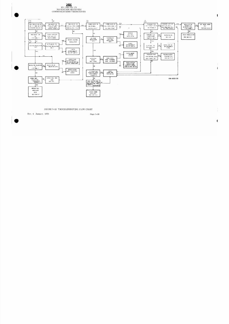
8/9/2019 KX 170A - Maintenance Manual Honeywell
http://slidepdf.com/reader/full/kx-170a-maintenance-manual-honeywell 128/586
KX 170A/KX 175
NAVIGATION RECEIVER/
COMMUNICATIONS TRANSCEIVER
El
NO
A
1
NAV INDICATION OK NAV AUDIO OK
NAV AUDIO OK
C OM M A UD IO OK
- YES
COMM AUDIO OK _ -
*
TRANSMITTER
TRANSMITTER CW
YES
YES
c MODULATON
SET MIKE
ON 113 5 MHZ WITH - W’T” ‘I3 5 MHz
YES
* ON ALL KHz120ea) -
YES
YES
C W PO WE R O K A T Y ES F RE O. O K O N A LL
CAPABILITY
YES
PDT
STANDARD NAV SIG 7
I
l O2 OH Z 3 0%
lVOlCE / IDENT)?
A ND A LL M Hz ( I O e a)
I
I?---
- 126.700 MHz
1 102OH1;30%7 1 1
ALL MHz(8a)~
- ALL KHz (20eo.I E
NO
126.700MHz 7
MHr( 8eo) AND ALL NO
OK WITH IKHr
KHz FREO (20ro I7 -
(.I25 VRMS)?
PER SEC.
I
,
I
IN0
CHECK MODULATOR
PER SEC. 5 .9
NO
REPAIR
VOLTAGE
I
YES
I
INTERCONNECT
O N- OF F S WI TC H
YES
I
CHECK
1
YES
I
YES
-I
CHECK NOISE
LIMITER
DETECTOR
AUDIO
OK? TP410
NO
INO
DOES CR431
= m H AV E F OR WA RD
BIAS VOLTAGE7
CHECK CARRIER
S OU EL CH A N)
t
NO
CARRIER TO NOISE
SWELCH PER SEC58
I
I S C OM M S MO
CHECK
I
v
INJECTION FREO _
YES
C OMM S MO
*
(135.700MHZ)
w
PER SEC 5.6
CORRECT 7
.
I
I
I
Y ES I NTE RCO NNE CT
RELAYS,ON-OFF SW.,
AUDIO POWER AMP-
DETECTOFtNAUDIO OK
AUDIO OK ON
PIN 35 OF Jl7l ?
I-
REPAIR AUDIO
NO
Y
A MP L C IR CU IT RY
NO
(I 403)
I
ISNAV SMO
INJECTION
FREOUENCY
RECEIVER
SECTION 5.7
-I
H EC K N AV S MO
NO
SEE
S EC . 5 .5
696-6052-00
.
I
CHECK COMM
RECEIVER
PER SEC 5.8
I
FIGURE 5-12 TROUBLESHOOTING FLOW CHART
Rev. 4 January, 1976
Page 5-30

8/9/2019 KX 170A - Maintenance Manual Honeywell
http://slidepdf.com/reader/full/kx-170a-maintenance-manual-honeywell 129/586
ZitG
KX 170A/KX 175
NAVIGATION RECEIVER/
COMMUNICATIONS TRANSCEIVER
5.4 TROUBLESHOOTINGHEKX 17OA/KX 75
Figure 5-12 is a troubleshooting flow chart designed to aid the technician in sectionalizing
or localizing sources of trouble.
NAV and COMM block diagrams Figure 5-48 and 5-49
appearing at the end of Section 5 may also aid in localizing the malfunction.
The trouble-
shooting charts (Table 5-5 thru 5-9) are given as a quick guide in pinpointing probable
problem areas along with their associated remedies. A list of possible SMO malfunctions
is given in the Preliminary Evaluation section of the respective SMO discussions (NAV
SMO, Section 5. 5, COMM SMO, Section 5. 6).
Individual circuit tracing and isolation of a defective component is most easily accomp-
lished by use of the individual troubleshooting sections,
along with appropriate schematic
diagrams appearing at the end of Section 5.
March, 1971
Page 5-31

8/9/2019 KX 170A - Maintenance Manual Honeywell
http://slidepdf.com/reader/full/kx-170a-maintenance-manual-honeywell 130/586
KING
KX 170A/KX 175
NAVIGATION RECEIVER/
COMMUNICATIONS TRANSCEIVER
TABLE 5-5 NAV SMO TROUBLE CHART
NDICATION
>ow or no output from
deceiver Buffer
Iorrect output on lower
requencies only.
?requency incorrect on
;ome positions of NAV
VIHz and KHz frequency
:ontrol.
Trequency error and/or
itter in Receiver Buffer
,utput.,
PROBABLE CAUSE
Voltage Regulated .Supply
(8. 5 and 5. 0 volts) com-
ponent failure.
Receiver Buffer com-
ponent failure.
VCO adjusted incorrectly.
Switching wafer defective.
Programmable Divider
component failure
Phase and Frequency com-
parator component failure.
REMEDY
Check QlOl, Ql03 and
CR214 voltages and
associated components.
Check Q202 voltages and
associated components.
Check VCO adjustment
L201.
See Alignment
Procedure.
Check switch wafer S 107
rear for MHz error.
See
Table 4-3.
Check switch wafer S105
for KHz error. See Table
4-3.
Check 1201, 1202, 1203,
1204 and 1206. A com-
parison can be made be-
tween the COMM and NA\
SMO’s using a signal gen-
erator
to drive the Squaring
Amplifier and an oscillo-
scope as a signal tracer.
See Troubleshooting Pro-
cedure.
Check 1205, 1207 and 1208
voltages and associated
components;
Check output at R215 with
an oscilloscope and. obser
waveform when switching
NAV MHz frequency contr
Page 5-32
*
March, 1.971
.
a

8/9/2019 KX 170A - Maintenance Manual Honeywell
http://slidepdf.com/reader/full/kx-170a-maintenance-manual-honeywell 131/586
is
Kx 170A/KX 175
NAVIGATION RECEIVER/
COMMUNICATIONS TRANSCEIVER
TABLE 5-5 NAV SMO TROUBLE CHART (Cant)
NDICATION
PROBABLE CAUSE
Trequency error in
Low Reference Oscillator
deceiver Buffer output.
400KHz component failure.
I
REMEDY
Check Q210 and Q211 volt
ages and associated camp
onents.
Check Y202 frequency at
T P205
High Reference Oscillator
53. 93125MHz component
failure.
Check Q207 voltages and
associated components.
Check Y201 frequency at
junction of R230 and H231
Divide by 2 Mixer and
amplifier component failure.
Check Q206 voltages and
associated components.
Check for frequency input
at TP203 and for divide b:
2 frequency output at TP2
Y
04
Squaring Amplifier com-
ponent failure.
Check Q208 and Q209 volt-
ages and associated comp-
onents.
Use an oscillo-
scope and check for an
essentially square wave
output at TP206.
Voltage Translator com-
ponent failure.
Check Q204 and Q205 volt-
ages and associated comp-
onents. Connect oscill-
oscope to TP202 and
observe waveforms when
switching NAV MHz freq-
uency control.
VCO Low Pass Filter com-
ponent failure.
(:heck at TP201 for a dc
voltage change as the NAV
MHz frequency control is
switched.
March, 1971
Page 5-33

8/9/2019 KX 170A - Maintenance Manual Honeywell
http://slidepdf.com/reader/full/kx-170a-maintenance-manual-honeywell 132/586
KING
Kx l’IOA/I(X 175
NAVIGATION RECEIVER/
COMMUNICATIONS TRANSCEIVER
TABLE 5-6
COMM SMO TROUBLE CHART
NDICAT ION
PROBABLE CAUSE
Jaw or no output from
Voltage Regulated Supply
deceiver Buffer
(8. 5 and 5. 0 volts) com-
ponent failure.
Receiver Buffer component
failure.
deceiver Buffer output
Transmit Buffer component
Nut no Transmit Buffer
failure.
utput in Transmit
:ondition.
Transmit Enable Switch
component failure.
Out of Lock Disable
REMEDY
Check Q102, Q105, Q104
and CR31 9 voltages and
associated components.
Check Q303 voltage and
associated components.
Check Q306 voltages and
associated components,
Check Q305 voltages and
associated components.
Check Q307 and input to
R323 with an oscilloscope
-ransmit Buffer output
n Receive condition.
deceiver Buffer and/or
‘ransmit Buffer, fre-
uency incorrect from
18. 00 to 126. 95MHz
ut OK from 127. 00 to
35MHz or vice versa.
Transmit Enable T ran-
sistor open.
COMM MHz HI;LO switch
wafer.
Transmit- Receive Relay
High Reference Crystals
Check Q305 voltages.
Check switch wafer S103.
Check relay K701.
Check i’301 and Y302 and
associated components,
Check switching diodes
CR313 and CR314 bias
voltages.
HI-LO VCO Switch Check switching diodes
CR301 and CR302, bias
voltages.
Page 5-34
March, 1971
a
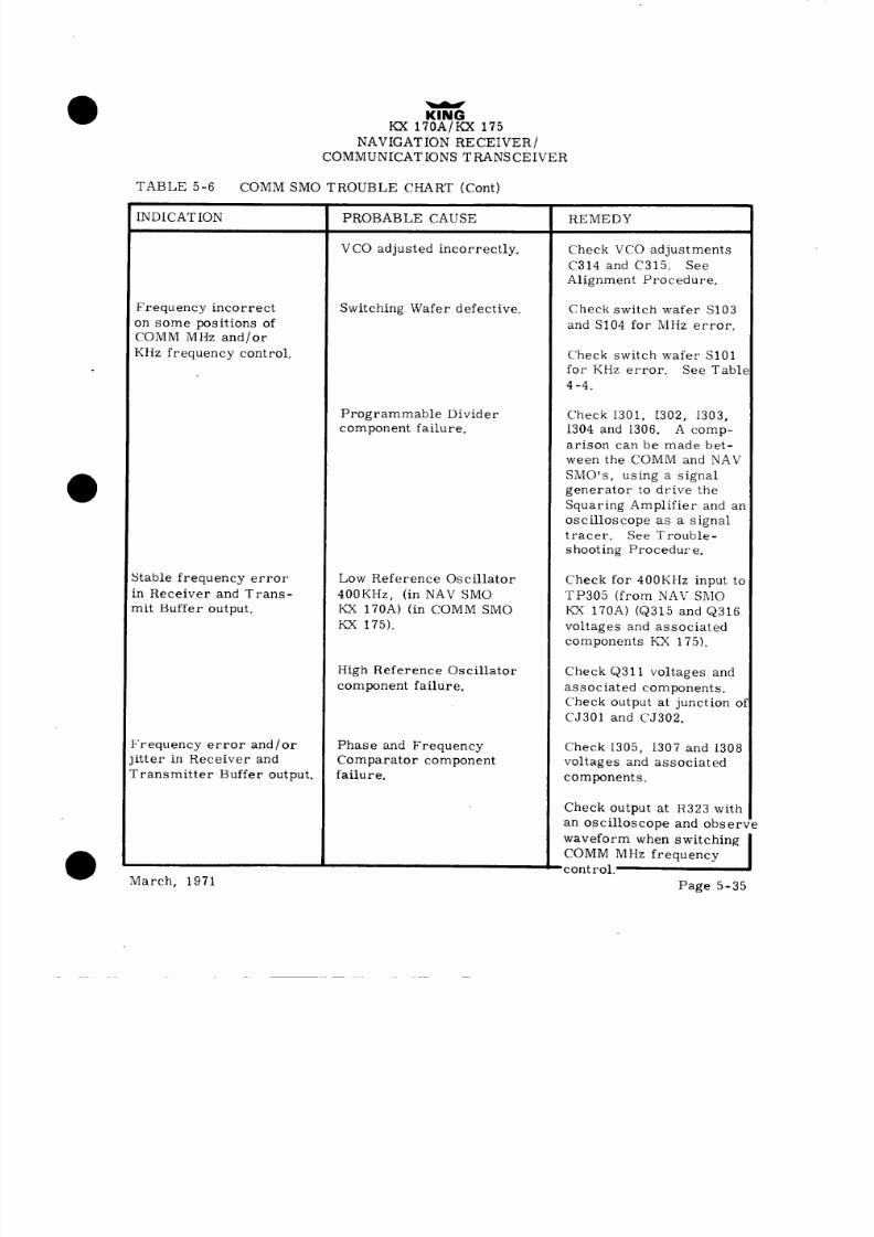
8/9/2019 KX 170A - Maintenance Manual Honeywell
http://slidepdf.com/reader/full/kx-170a-maintenance-manual-honeywell 133/586
m
KX 17OA/KX 175
NAVIGATION RECEIVER/
COMMUNICATIONS TRANSCEIVER
TABLE 5-6 COMM SMO TROUBLE CHART (Cant)
INDICATION
Frequency incorrect
3n some positions of
COMM MHz and/or
KHz frequency control.
stable frequency error
in Receiver and Trans -
nit Buffer output.
Trequency error and/or
itter in Receiver and
rransmitter Buffer output.
March, 1971
PROBABLE CAUSE
VCO adjusted incorrectly.
Switching Wafer defective.
Programmable Divider
component failure.
LOW Reference Oscillator
400KHz, (in NAV SMO
Kx 170A) (in COMM SMO
Kx 175).
High Reference Oscillator
component failure.
Phase and Frequency
Comparator component
failure.
REMEDY
Check VCO adjustments
C314 and C315. See
Alignment Procedure.
Check switch wafer S103
and S104 for MHz error.
Check switch wafer SlOl
for KHz error. See Table
4-4.
Check 1301, 1302, 1303,
1304 and 1306. A comp-
arison can be made bet-
ween the COMM and NAV
SMO’s, using a signal
generator to drive the
Squaring Amplifier and an
oscilloscope as a signal
tracer.
See Trouble-
shooting Procedure.
Check for 400KHz input tc
TP305 (from NA\: SIz,lO
Kx 170A) (Q315 and Q316
voltages and associated
components KX 175).
Check Q311 voltages and
associated components.
Check output at junction o
CJ301 and CJ302.
Check 1305, 1307 and 1308
voltages and associated
components.
Check output at R323 with
an oscilloscope and obser
waveform when switching
‘cent rol.i
COMM MHz frequency
Page 5-35

8/9/2019 KX 170A - Maintenance Manual Honeywell
http://slidepdf.com/reader/full/kx-170a-maintenance-manual-honeywell 134/586
Kx lBi?i%ix 175
NAVIGATION RECEIVER/
COMMUNICATIONS TRANSCEIVER
TABLE 5-6
COMM SMO TROUBLE CHART (Cont. )
[ND ICAT ION
PROBAB I.,E CAUSE
< REMEDY
Frequency error’ and/or
Low Reference Oscillator
Check for 400KHz input tc
jitter in Receiver and 40OKHz (in NAV SMO KX 170A) TP305. D
rransmitter nuffer output. (in COMM SMO f<X 175)
High Reference Oscillator
Check Q311 voltages and
component failure.
associated components.
Check output at junction
of CJ301 and CJ302.
Divide by 2 Mixer and
Amplifier component
failure.
. Check Q310 voltages and
associated components.
Check for frequency
inpu
at Q304 collector and for
divide by 2 frequency out
put at ‘I‘P304.
Squaring Amplifier com-
ponent failure.
Check Q312 and Q313
v01
ages and associated corn1
onents,
Lise an oscillo-
scope and check for an
essentially square wave
o~~?put at TP306,
Voltage ‘l‘ranslator com-
ponent failure,
C‘heck (~308 and Q309
voltages and associated
components.
Connect
oscilloscope to ‘I‘P302
an
observe waveform when
switching COMM hIH2
frequency control.
VCO Low Pass Filter
component failure
Check at ‘I.P3$Il for a dc
volt.age change as the
C:OMM MHz frequency
control is switched.
Page 5-36
March, 1971
a’

8/9/2019 KX 170A - Maintenance Manual Honeywell
http://slidepdf.com/reader/full/kx-170a-maintenance-manual-honeywell 135/586
KING
KX 170A/KX 175
NAVIGATION RECEIVER/
COMMUNICATIONS TRANSCEIVER
TABLE 5-7 NAV RECEIVER TROUBLE CHART
NDICAT ION
Jo reception ‘,
leadphone output but
ow or no speaker
,utput.
PROBABLE CAUSE
“OFF-ON” switch
8. 5vdc regulator
5. Ovdc regulator
Receiver board com-
ponents.
NAV SMO no local os-
cillator output or wrong
frequency.
NAV Receiver, second
local oscillator.
Fuse blown
COMM Speaker “OFF-ON”
switch in “OFF” position
or defective.
Transmit-Receive relay
Audio board component
failure.
Audio Output transistor
REMEDY
Check switch S112
Check Ql
01 and Q103 volt
ages and
associated camp
onents.
Check CR214
Check voltages and com-
ponents.
Check voltages and low
frequency reference os-
cillator Q210, Q211 and
high frequency reference
oscillator Q207 frequencic
Check VCO adjustment
L201.
See Alignment
Procedure.
Check Q408 voltages and
Y401 frequency.
Check fuse F701
(KX 17OA/KX 175 Only)
Check switch SllO.
Check relay K701
Check CR701, CR702, Q7
3.
1,
Q702 voltages and associat-
ed component.
Check Q703, Q704, Q705
and Q706
Page 5-37
Rev. 2, December, 1972

8/9/2019 KX 170A - Maintenance Manual Honeywell
http://slidepdf.com/reader/full/kx-170a-maintenance-manual-honeywell 136/586
ZiK
KX 170A/KX 175
NAVIGATION RECEIVER
COMMUNICATIONS TRANSCEIVER
TABLE 5-7 NAV RECEIVER TROUBLE CHART (CONT)
I
INDICATION
I
Receiver sensitivity
weak
Audio weak or distorted
4GC circuit inoperative
[ndicator error on strong
signals
1
14GC motorboating
I
Vo attenuation of VOR
1dent signal with “Voice/
I:dent” switch in “Voice”
1
x)s ition.
I
Vo VOR/ L,OC signal
(xltput
Page 5-38
PROBABLE CAUSE
Defective component in
R- F or I-F amplifier
circuits or alignment
Low SMO signal to 1st
mixer.
Audio amplifier on
receiver board
Audio board component
failure
Audio output transistors
AGC transistors
AGC capacitors open
Voice/Ident switch
Ident filter
VOR/ LOC level adjust-
ment control or output
coupling capacitor open
REMEDY
Check voltage and compor
ents.
See Alignment
Procedure.
Check NAV SMO
Check 1403 voltages and
associated components.
Check CR701, CR702,
Q701, Q702 voltages and
associated components.
Check Q703, Q704, Q705
and Q706.
Check Q406, Q407, CR411
and associated component
Check C441 and C442
Check switch Sill
Check L703 and C716
L703 not adjusted to 1020
KHz. See Alignment
Procedure.
Check adjustment of R425
See Alignment Procedure,
Check C443
March, 1971
a

8/9/2019 KX 170A - Maintenance Manual Honeywell
http://slidepdf.com/reader/full/kx-170a-maintenance-manual-honeywell 137/586
ECX 17OA/KX 175
NAVIGATION RECEIVER/
COMMUNICATIONS TRANSCEIVER
TABLE 5-8
COMM RECEIVER TROUBLE CHART
VDICAT ION
‘0 reception
0 reception from
18. 00 to 126. 95MHz
It OK from 127.00
I 135. 95MHz or vice
?rsa.
PROBABLE CAUSE
“OFF-ON” switch
8. 5vdc regulator
5. Ovdc regulator
Receiver board component
failure.
COMM SMO 400KHz refer-
ence 0s cillator
COMM SMO no local oscil-
lator output or wrong freq-
uenc y
Audio board component
failure.
COMM Receiver second
local oscillator
COMM SMO High Freq-
uency crystals
COMM SMO HI-LO ,VCO
switch
COMM MHz HI-LO switch
wafer
Transmit-Receiver relay
REMEDY
I
Check switch SllO
I
Check Q102, Q105 and Q104
voltages and associated
components.
Chec.k CR3 19
Check voltages and com-
ponents.
Check Q3 15, Q316, Y303
and associated component
.S
eheck voltages, referent’
frequencies and VCO ad-
justments C314 and C315.
See Alignment Procedure,
11
heck CR701, CR702, Q7C
Q702 voltages and assoc-
iated components.
Check Q409 voltages and
Y402 frequency.
Check CR313 and CR314
bias voltages,
Check Y301 and Y302 and
associated components.
Check CR301 and CR302
bias voltages and VCO
adjustments C314 and C31
See Alignment Procedure.
Check switch wafer S103
Check relay K701
Page 5-39
arch, 1971
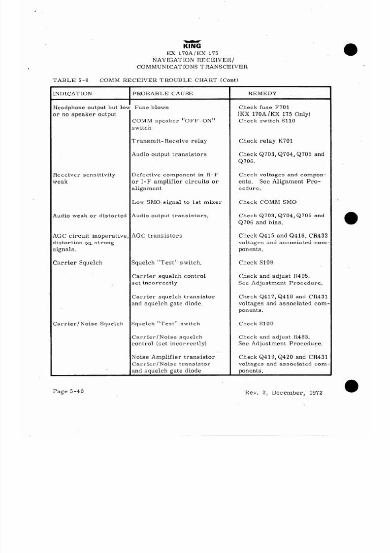
8/9/2019 KX 170A - Maintenance Manual Honeywell
http://slidepdf.com/reader/full/kx-170a-maintenance-manual-honeywell 138/586
KING
KX 170A/KX 175
NAVIGATION RECEIVER/
COMMUNICATIONS TRANSCEIVER
TABLE 5-8
COMM RECEIVER TROUBLE CHART (Cant)
:NDICAT ION
I
PROBABLE CAUSE
Jeadphone output but lo
)r no speaker output
seceiver sensitivity
veak
Audio weak or distorted
JGC circuit inoperative
listortion on strong
signals.
Zarrier Squelch
3arrier/ Noise Squelch
Page 5-40
Fuse blown
COMM speaker “OFF-ON”
switch
Transmit-Receive relay
Audio output transistors
Defective component in R-F
or I-F amplifier circuits or
alignment
Low SMO signal to 1st mixer
Audio output transistors.
AGC transistors
Squelch “Test” switch.
Carrier squelch control
set incorrectly
Carrier squelch transistor
and squelch gate diode.
Squelch “Test” switch
Carrier/Noise squelch
control (set incorrectly)
Noise Amplifier transistor
Carrier/Noise transistor
and sauelch gate diode
REMEDY
Check fuse F701
(KX 170A/KX 175 Only)
Check switch SllO
Check relay K701
Check Q703, Q704, Q705 and
Q706.
Check voltages and compon-
ents. See Alignment Pro-
cedure.
Check COMM SMO
Check Q703, Q7Q4, Q705 and
Q706 and bias.
Check Q415 and Q416, CR432
voltages and associated corn.
ponents.
Check S109
Check and adjust R495.
See Adjustment Procedure.
Check Q417,Q418 and CR431
voltages and associated corn.
ponents.
Check S109
Check and adjust R483.
See Adjustment Procedure.
Check Q419, Q420 and CR431
voltages and associated corn.
ponents.
Rev. 2, December, 1972

8/9/2019 KX 170A - Maintenance Manual Honeywell
http://slidepdf.com/reader/full/kx-170a-maintenance-manual-honeywell 139/586
m
KX 170A/KX 175
NAVIGATION RECEIVER/
COMMUNICATIONS TRANSCEIVER
TABLE 5-9 COMM TRANSMITTER TROUBLE CHART
NDICATION
Jo transmitter CW output
ro transmitter CW output
rom 118. 00 to
126. 95MHz
ut OK from 12 7. 00 to
35. 95MHz or vice versa
row cw output
PROBABLE CAUSE
No excitation from COMM
SMO
Transmitter component
failure
Supply voltage or D-C
bias incorrect
Diode T-R switch shorted
COMM SMO high frequency
reference crystals
COMM SMO HI-LO VCO
switch
COMM MHz HI-LO switch
wafer
Transmit-Receive Relay
Transmitter component
failure
REMEDY
Check transmit buffer, Q306,
transmit disable Q307 volt-
ages and associated compon-
ents.
Trace R-F signal with oscil-
10s cope
probe
QSOl, Q602, Q603 and Q604.
Remove RF excitation from
transmitter by setting COMN
MHz frequency control at un-
marked positions between
118. 00 to 135. OOMHz.
Check D-C bias on QSOl,
Q602 and Q603.
Check diode CR603
Check CR313 and CR314 bias
voltages
Check Y301 and Y302 bias
voltages and VCO adjustment
C314 and C315. See align-
ment procedure.
Check switch wafer S103
Check relay K701
Check R-F signal and gain
with oscilloscope probe from
input thru Q601, Q602, Q603,
Q604 and low pass filter out-
put.
March, 1971
Page 5-41
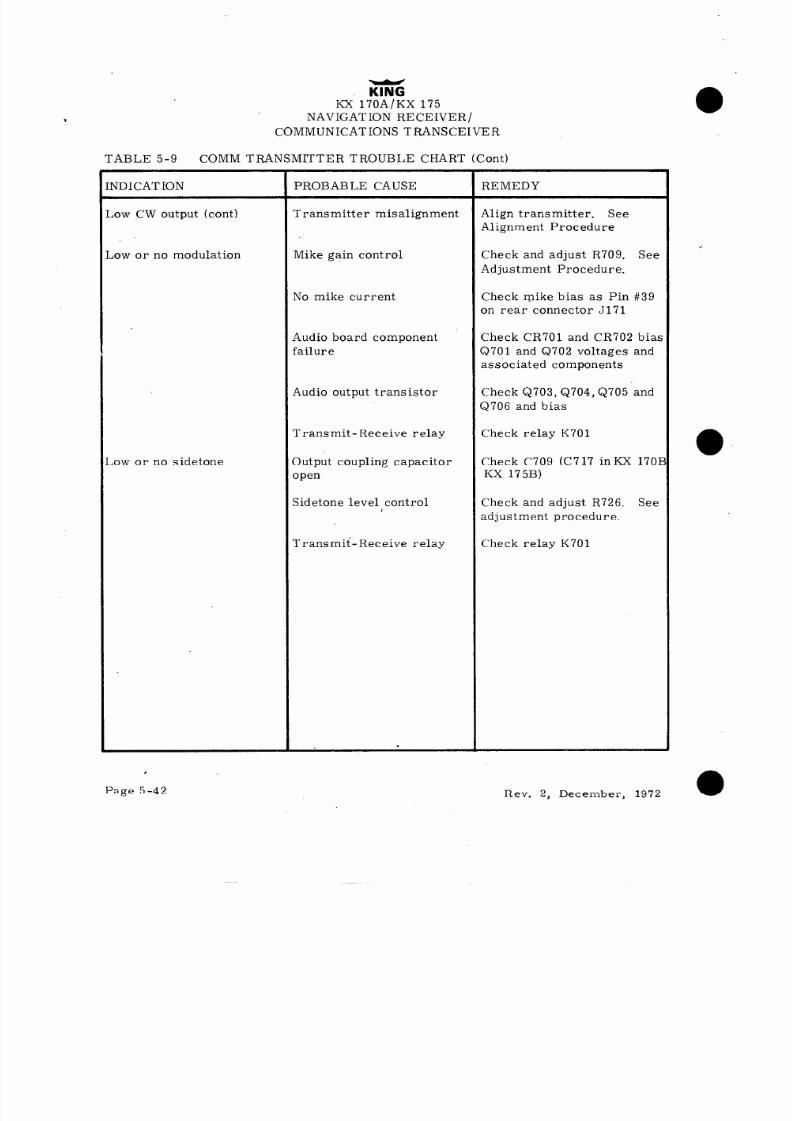
8/9/2019 KX 170A - Maintenance Manual Honeywell
http://slidepdf.com/reader/full/kx-170a-maintenance-manual-honeywell 140/586
.m
KX 17OA/KX 175
NAVIGATION RECEIVER/
COMMUNICATIONS TRANSCEIVER
TABLE 5-9
COMM TRANSMITTER TROUBLE CHART (Cant)
NDICAT ION
Aow CW output (cant)
Jow or no modulation
iow or no sidetone
PROBABLE CAUSE
REMEDY
Transmitter misalignment
Align transmitter. See
Alignment Procedure
Mike gain control
Check and adjust R709, See
Adjustment Procedure.
No mike current
Check mike bias as Pin #39
on rear connector 5171
Audio board component Check CR701 and CR702 bias
failure
Q701 and Q702 voltages and
associated components
Audio output transistor
Check Q703, Q704, Q705 and
Q706 and bias
Transmit-Receive relay
Check relay K701
Output coupling capacitor
Check C709 (C717 inKX 1701
open
KX 175B)
Sidetone level control
I
Check and adjust R726. See
adjustment procedure.
Transmit-Receive relay
Check relay K701
.
i
l
Page 5-42
Rev. 2, December, 1972
a
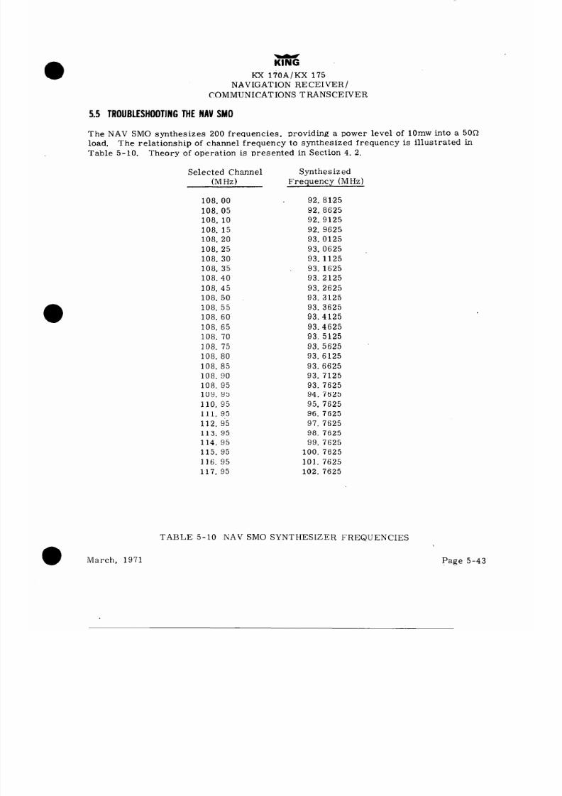
8/9/2019 KX 170A - Maintenance Manual Honeywell
http://slidepdf.com/reader/full/kx-170a-maintenance-manual-honeywell 141/586
KING
KX 17OA/KX 175
NAVIGATION RECEIVER/
COMMUNICATIONS TRANSCEIVER
5.5 TROUBLESHOOTINGHENAVSMO
The NAV SMO synthesizes 200 frequencies,
providing a power level of 1Omw into a 500
load. The relationship of channel frequency to synthesized frequency is illustrated in
Table 5-10. Theory of operation is presented in Section 4. 2.
Selected Channel
(MHz)
Synthesized
Frequency (MHz)
108. 00
92. 8125
108. 05
92. 8625
108. 10
92.9125
108. 15 92. 9625
108. 20 93. 0125
108. 25
93. 0625 _
108. 30 93. 1125
108. 35 93. 1625
108. 40
93. 2125
108. 45 93. 2625
108. 50 93. 3125
108. 55 93. 3625
108. 60
93.4125
108. 65 93.4625
108. 70 93. 5125
108. 75 93. 5625
108. 80 93. 6125
108. 85 93. 6625
108. 90 93. 7125
108. 95
93. 7625
109. 95
94. 7625
110.95 95. 7625
111. 95 96. 7625
112. 95 97. 7625
113. 95
98, 7625
114. 95
99. 7625
115.95
100. 7625
116. 95
101. 7625
117.95
102. 7625
TABLE 5-10 NAV SMO SYNTHESIZER FREQUENCIES
March, 1971
Page 5-43

8/9/2019 KX 170A - Maintenance Manual Honeywell
http://slidepdf.com/reader/full/kx-170a-maintenance-manual-honeywell 142/586
,wl
KING
KX 17OA/KX 175
NAVIGATION RECEIVER /
COMMUNICATIONS TRANSCEIVER
5. 5, 1 PRELIMINARY EVALUATION (Figure 5-50)
A.
Verify the NAV SMO failure
1.
Perform the alignment procedure of Section 5. 2. 1.
2.
Does the NAV SMO supply 1Omw to a 50 ohm load?
3. IS the synthesized frequency correct when dialing through all KHZ (20 each)
and all MHz (10 each) positions with both clockwise and counterclockw ise
rotation?
B.
Is the failure external from the NAV SMO enclosure?
1. Check all power and control lines to the NAV SMO for proper operation.
Wire color and feedthru assignments
Control wire functions are defined in
and “1” is 5vdc.
2.
Is there a short circuit in the COMM
the NAV SMO (KX 170A only)?
5.5.2 NAV SMO DIAGNOSTIC PROCEDURE
are shown in Figure 5-50.
Table 4--3 where “0” is ground potential
SMO disabling the 4OOKHz oscillator in
l
If the tests of 5. 5. 1 substantiate the NAV SMO failure, proceed as follows:
A. Open the Loop
-NOTE-
To properly troubleshoot the NAV SMO, it
is imperative that the feedback loop be dis-
abled.
This is accomp lished very simply
by applying a positive, O-10 volt adjustab le
D-C voltage from a low impedance source
to TP201, the VCO bias point.
B.
Is the High Reference Oscillator Operating Properly?
Using a 1Kpf capacitor, connect a VHF frequency counter to the junction of R230 and R231
in the High Reference Oscillator and check for 53. 93125MHz.
If the oscillator is inoper-
ative or off frequency,
refer to section 5. 5. 11 for servicing information.
Page 5-44
March, 1971

8/9/2019 KX 170A - Maintenance Manual Honeywell
http://slidepdf.com/reader/full/kx-170a-maintenance-manual-honeywell 143/586
KING
KX 170A/KX 175
NAVIGATION RECEIVER/
COMMUNICATIONS TRANSCEIVER
C.
Is the Low Reference Oscillator Operational?
Connect a frequency counter to TP205 in the Low Reference Oscillator and measure
400. OOOKHz. Remove the counter coax, connect an oscilloscope to TP205 and observe
the waveform of Figure 5-13. If a malfunction is observed, refer to Section 5. 5. 5 for
servicing instructions.
1
I
I
I :
: I
.---.-; .----.-----: ----,----,--ee-
4
,
1
7
3V
I.
-cl .5ySeCL
. 96-6053-00
FIGURE 5-13 LOW REFERENCE OSCILLATOR OUTPUT
Does the VCO and Receiver Buffer Perform Properly?
Dial 116. 70MHz on the NAV frequency selector and adjust the VCO bias voltage to
6. 50V.
Connect a VHF counter to the VCO Buffer, TP203, and adjust L201 to obtain a
frequency of approximately 101. 5125MHz. Erratic or improper tuning, or low output
should be corrected by troubleshooting the VCO and/or VCO Buffer as outlined in
Sections 5. 5. 6 and 5. 5. 10.
E.
Is the Implicit Divide by 2 Halving the VCO Frequency?
Without altering the tuning voltage or the channel frequency setting connect the VHF
counter to TP204 and read a frequency of approximately 50. 756MHz.
If a malfunction is
observed, the circuit may be serviced as outlined in the troubleshooting instructions of
Section 5. 5. 12.
March, 1971
Page 5-45

8/9/2019 KX 170A - Maintenance Manual Honeywell
http://slidepdf.com/reader/full/kx-170a-maintenance-manual-honeywell 144/586
m
KX 170A/KX 175
NAVIGATION RECEIVER/
COMMUNICATIONS TRANSCEIVER
F.
Is the Mixer Working Properly?
With 116. 70MHz selected and 6. 50vdc bias applied to the VCO as in previous steps,
con-
nect an oscilloscope to the junction of L204, C240 and C241.
The waveform should be of
the approximate amplitude and frequency of Figure 5-14.
Failure to obtain the desired
trace would indicate a malfunction in the Mixer circuit which can be serviced as outlined
in the troubleshooting instructions of Section 5. 5. 13.
Vertical:
0. 05V/div
Horizontal:
0. lpsec/div
Selected Freq. : 116. 70MHz
FIGURE 5-14 MIXER OUTPUT
696-6054-00
G* .
s the. Squaring Amplifier in Good Health?
With the VCO oscillating near 101. 5125MHz (NAV frequency selector at 116. 70MHz)
monitor the Squaring Amplifier output,
TP206, with an oscilloscope having a bandwidth
of at least 30MHz.
If the high reference oscillator is functioning properly, the wave-
form will appear as in Figure 5-15.
If not, troubleshoot the squaring amplifier as in
Section 5. 5. 15.
Page 5-46
March, 19 71
a

8/9/2019 KX 170A - Maintenance Manual Honeywell
http://slidepdf.com/reader/full/kx-170a-maintenance-manual-honeywell 145/586
izix
KX 170A/KX 175
NAVIGATION RECEIVER/
COMMUNICATIONS TRANSCEIVER
Vertical: 1’V/DIV
Horizontal:
. lpsec/DIV
Selected Freq:
116. 700MHz
Squaring Amp. Freq, :
3. 175MHz
696-6055-00
FIGURE 5-15 SQUARING AMPLIFIER OUT PUT
H.
Does the Programmable Divider Provide Proper Frequency Division?
Short, test points, TP207, TP208, and TP209.
This disables the phase and frequency
comparator to permit testing of the programmable counter. Maintain the channel
setting and the VCO tuning voltage of Steps D through G.
Attach the oscilloscope probe
to Pin 9 of 1202 or 1206 to monitor the counter output.
The waveform of Figure 5-16
should be obtained. Note the pulse period of approximately 40psec.
Dial the ten MHz
positions, leaving the VCO bias unchanged,
and look for the counter output pulse rate to
increase uniformly as lower channel frequencies are dialed,
Return the MHz dial to the
116MHz position and dial through the twenty KHz positions.
Observe a gradual advance
in output pulse rate as numbers are dialed from the 0. 95 to . 00 using counterclockwise
rotation.
If erroneous operation of the Programmable Counter is observed, service the counter
using the procedure of Section 5. 5. 3.
Upon completion of the counter checks, remove
the shorting connections from test points TP207, TP208 and TP209.
March, 1971
Page 5-47

8/9/2019 KX 170A - Maintenance Manual Honeywell
http://slidepdf.com/reader/full/kx-170a-maintenance-manual-honeywell 146/586
KING
KX 170A/KX 175 -
NAVIGATION RECEIVER/
COMMUNICATIONS TRANSCEIVER
Horizontal: Spsec/Div
Trace: C250, C248, CR213
Vertical: 2V/Div
696
~60 56 -00
FIGURE 5-16 PROGRAMMABLE DIVIDER OUTPUT
I.
Is the Phase and Frequency Comparator Operational?
Connect the oscilloscope probe to the junction of Pins 1, 5 and 10 of 1208 and R215 to
monitor the Phase and Frequency Compara tor output.
With the channel selector at
116. 70MHz, vary the VCO bias voltage above and below 6. 50 volts.
The output voltage
on the scope should be dominately high when the VCO bias is low, and low when the
VCO bias is high. Waveforms are illustrated on the “set-reset” output “Q” of the Phase
and Frequency Compara tor Timing Diagrams of Figure 5-33.
If a malfunction is noted,
troubleshoot the circuit as illustrated in Section 5. 5. 4.
J.
Does the Voltage Translator Operate Properly?
Repeat the test of Ste,p I but with the oscilloscope probe attached to TP202.
Waveforms
are illustrated in Figure 5-17.
Service the circuit as required using the reference infor-
mation of Section 5. 5. 8.
Page 5-48
March, 1971
l

8/9/2019 KX 170A - Maintenance Manual Honeywell
http://slidepdf.com/reader/full/kx-170a-maintenance-manual-honeywell 147/586
KING
KX 170A/KX 175
NAVIGATION RECEIVER/
COMMUNICATIONS TRANSCEIVER
Horizontal: 5psec/Div
Upper Trace: Comparator Output (Pins 1, 5, and 10 of
1208)
Upper vertical: lV/Div
Lower Trace:
Translator Output (T P202)
Lower Vertical: 2V/Div
696-6057-00
FIGURE 5 - 17 VOLTAGE TRANSLATOR
K. What if no Problems are Observed?
Troubleshoot the remaining block, the VCO Low Pass Filter per the discussion of
Section 5. 5. 7.
March, 1971 Page 5-49
8/9/2019 KX 170A - Maintenance Manual Honeywell
http://slidepdf.com/reader/full/kx-170a-maintenance-manual-honeywell 148/586
KING
KX 170A/KX 175
NAVIGATION RE CEIVER /
COMMUNICA’I’IONS TRANSCEIVER -o
5. 5. 3 PROGRAMMABLE DIVIDER (FIGURE 5-19)
The Programmable Divider consists of integrated circuits 1201, 1202, 1204, 1206 and
gates A and D in 1203.
Reference material includes the divider theory of Section 4
and the Timing Diagram of Figure 5-32,
-NOTE-
If the COMM SMO is functioning properly,
the servicing technician has the option of
using comparison techniques in trouble-
shooting the NAV SMO.
5. 5. 3. 1
Troubleshooting Procedure.
I.
Test Setup
A.
‘Open either end of L204, the Mixer Low Pass Filter choke.
B.
Short Pins TP207, TP208 and TP209 together.
C.
Use a coaxial pigtail to connect an HP 606A, or equivalent, to the tie point
of C240 and C241.
II.
Equipment Adjustments
A.
Using a frequency counter, set the 606A, to a CW frequency of 3. 175MHz.
B.
Adjust the HP 606A CW level to obtain a crisp square wave (0 volts base
line, 4 volts peak line) at TP206, when viewed by a 30MHz bandwidth or
wider oscilloscope.
C.
Dial the NAV channel selector to 116. 70MHz.
If comparison techniques are
to be used select either 126. 6OMHz or 135. 70MHz for the COMM channel.
III. Observations
A.
Use a 30MHz bandwidth (or wider) oscilloscope.
Provide external sync
from the leading edge of the pulse appearing at the junction of R248 and
CR213.
B.
Compare the waveform at Pin 6 of the 1204 to the equivalent point in the
COMM SMO or to the timing diagrams.
The desired output is a pulse train
Page 5-50
March, 1971

8/9/2019 KX 170A - Maintenance Manual Honeywell
http://slidepdf.com/reader/full/kx-170a-maintenance-manual-honeywell 149/586
KING
KX 170A/KX 175
NAVIGATION RECEIVER/
COMMUNICATIONS TRANSCEIVER
with a 4 volt reference level, a 40psec period (25KHz rep ratej, negative
pulse width of approximately 2lOnsec,
and 0 volts negative excursion.
C.
If the desired oscilloscope trace was obtained in B, the counter is operational
at 116. 70MHz.
Dial 117. 950MHz. With the oscilloscope sync as in A on
preceeding page, simultaneously monitor TP206 and Pin 9 of 1208.
Note the
relationship of the pulses as the dial is rotated sequentially to the next low-
est channel.
The output pulse (Pin 9 of 1208) should step 1 input pulse in-
crement with each 50KHz
step in dialing.
See Figure 5-18. If the counter
is 01
Selected Freq. = 116. 70MHz
Selected Freq. = 116. 65MHz
Vertical: Top-lV/div (TP206)
Bottom - O.‘5V/div (Pin 9 of 1208)
Horizontal:
0. 5psec/div
696-6106-00
FIGURE 5-18 PROGRAMMABLE DIVIDER
D.
Failure to meet the requirements of Step B requires a complete check of the
I-C input/output timing as defined in either the Timing Diagram (Figure
5-32 or an operable COMM or NAV SMO.
E.
Failure to meet the requirements of Step C implies a problem with the preset
function of the Programmable Divider,
Make a complete check of the divider
flip-flops immediately preceeding and following the preset enable pulse
(negative pulse on Pin 6 of 1204.
The desired preset states are defined in
Table 4-3, where 0 is ground and 1 is 5 volts,
and should occur immediately
following the preset enable pulse. Also review Figure 5-32.
F.
Replace components and make repairs as necessary to obtain the desired
counter operation.
March; 1971
Page 5-51

8/9/2019 KX 170A - Maintenance Manual Honeywell
http://slidepdf.com/reader/full/kx-170a-maintenance-manual-honeywell 150/586
KING
KX 170A/KX 175
NAVIGATION RECEIVER/
COMMUNICATIONS TRANSCEIVER
5. 5.4 PHASE AND FREQUENCY COMPARATOR (Figure 5-19)
The Phase and Frequency Comparator consists of integrated circuits 1205, 1207, 1208,
gates C and B of 1203 and wave shaping networks composed of C249, C250, C269, R24’i,
H248 and CR213.
Reference information sources include the Phase and Frequency
Comp&ator Timing Diagrams of Figure 5-33 and the theory of Section 4. 2.
-NOTE-
If the COMM SMO is operating properly
it may be used to provide supplementary
information using comparison techniques.
5. 5. 4. 1 Troubleshooting Procedure
A.
Connect an external power supply to the VCO bias test point TP201.
B.
Monitor the Comparator output (Pins 1, 5, or 10 of 1208) on an oscilloscope.
C.
Adjust the VCO bias voltage low (less than 6. 50 volts) and look for a high out-
put voltage (around 1. 5 volts). Refer to Figure 5-33 for the appropriate timing
diagram.
D.
Adjust the VCO bias voltage high (greater than 6. 50 volts) and look for a low
voltage output voltage (near ground potential).
Refer to Figure 5-33 for the
appropriate timing.
E.
Failure to meet the conditions of Steps C and D requires a systematic com-
parison of the input (output) relationships obtained to those appearing in either
the Timing Diagram or the functioning COMM SMO.
1.
Disable the counter hold pulses by shorting test points TP207, TP208 and
TP209 and check the divide by 16 block (1205) for proper 2, 4, 8 and 16 ripple
counter operation.
2.
Check the differentiation networks for proper waveshaping (tie point of C250,
CR213, R248 and the tie point of C249 and R247).
3.
Remove the shorting connections at test points TP207, TP208 and TP209.
Repeat the tests of Steps C and D.
If proper operation is still not obtained
monitor the gates of the MC817P’s (1207 and 12081 and B and C of 1204
I
for proper operation.
Page 5-52
March,, 1971
l

8/9/2019 KX 170A - Maintenance Manual Honeywell
http://slidepdf.com/reader/full/kx-170a-maintenance-manual-honeywell 151/586
iti%
KX 170A/KX 175
NAVIGATION RECEIVER /
COMMUNICATIONS TRANSCEIVER
5. 5.5 LOW REFERENCE OSCILLATOR (Figure 5-19 NAV) (5-29, COMM)
The Low Reference Oscillator consists of transistors Q210 (Q315) and Q211 (Q316),
with crystal Y202 (Y303) as the frequency determining element.
The Low Reference
Oscillator serves both the NAV and COMM SMO’s.
(KX 170A only).
5. 5. 5. 1
Troubleshooting Procedures. Using an oscilloscope check TP205 (TP305)
for a square wave output (See Figure 5-13). Capacitively couple a frequency counter
to TP205 (TP305) and check for 400KHz.
Check Q210 (Q315) and Q211 (Q316) and the
associated circuitry. See Figure 5-50 and 5-51 for typical D-C operating voltage levels.
March, 1971
Page 5-53

8/9/2019 KX 170A - Maintenance Manual Honeywell
http://slidepdf.com/reader/full/kx-170a-maintenance-manual-honeywell 152/586
KNG
KX 170A/KX 175
NAVIGATION RECEIVER /
COMMUNICATIONS TRANSCEIVER
t SYUC I
r--'
P RO G RA MM AB LE D IV D E R 1 r -
I I I I lr-
I
r
t
I ‘“DL
r
COMPARATOR
Low REFERENCE 0%.
FIGURE 5-19
NAV LOW REFERENCE OSCILLATOR/PROGRAMMABLE DIVIDER/
PHASE AND FREQUENCY COMPARATOR
March, 1971
Page

8/9/2019 KX 170A - Maintenance Manual Honeywell
http://slidepdf.com/reader/full/kx-170a-maintenance-manual-honeywell 153/586
m
KX 17OA/KX 175
NAVIGATION RECEIVER /
COMMUNICATIONS TRANSCEIVER
5.5. 6 VOLTAGE CONTROLLED OSCILLATOR (VCO) (Figure 5-20)
The Voltage Controlled Oscillator (Q201) is a Colpitts oscillator.
Frequency determining
elements include CR201, L201, C204 and C205.
Basic theory appears in Section 4. 2. 2. 2.
5. 5. 6. 1
Troubleshooting Procedure.
Compare the supply and bias voltages for Q201
with those appearing in Figure 5-50 and replace components as necessary to obtain pro-
per bias.
Apply a 7. 2 volt tuning bias voltage,
from a low impedance source, to TP201
and use a frequency counter to monitor the frequency at the collector of Q201. Adjust
L201 to obtain a frequency of approximately 102. 7625.
The VCO frequency should vary
proportionately as the tuning voltage is varied.
If erratic or erroneous operation is
obtained, check the frequency determining elements. Failure of the VCO to oscillate
implies an open varactor diode (CR201), an open trimmer coil (L201), or a bad transis-
tor (Q201).
5. 5. 7 VCO LOW PASS FILTER (Figure 5-20)
The VCO Low Pass Filter consisting of T201, C211, C212 and C213 is an elliptic low
pass filter designed to recover the D-C voltage from the output o f the 25KHz Voltage
Translator.
It has been factory adjusted and no attempt should be made to readjust in
the field.
Using an oscilloscope,
check for a square wave
check for a D-C voltage at TP201 (7. BOVDC at
5. 5.
7. 1 Troubleshooting Procedure.
input at TP202.
Using a D-C voltmeter,
117. 95MHz
to 2. 84VDC at 108. OOMHz.
5.5.8 25KHz VOLTAGE TRANSLATOR
(Figure 5-20)
The Voltage Translator consists of transistors Q204 and Q205 which shifts the error
voltage level from the Phase and Frequency Comparators to a level sufficient to operate
the VCO.
5. 5. 8. 1
Troubleshooting Procedure.
Using an oscilloscope trace the input signal
from R215 to the output of TP202.
See Figure 5-50 for typical D-C operating voltage
levels _
5. 5. 9 RECEIVER BUFFER (Figure 5-20)
The Receiver Buffer consists of transistor, Q202, with output transformer, T202.
5. 5. 9. 1
Troubleshooting Procedure.
Using an oscilloscope, trace the input signal
from C216 to the output at Pin 2 of T202.
See Figure 5-50 for typical D-C operating
voltage levels.
March, 1971
Page 5-57

8/9/2019 KX 170A - Maintenance Manual Honeywell
http://slidepdf.com/reader/full/kx-170a-maintenance-manual-honeywell 154/586
KING
KX 170A/KX 175
NAVIGATION RECEIVER /
CQMMUNICATIONS TRANSCEIVER
5.5. 10 VCO BUFFER (Figure 5-20)
’
he VCO Buffer consists of transistor Q203 with output transformer T203.
5. 5. 10. 1 Troubleshooting Procedure. Using an oscilloscope, trace the input signal
from C220 to the output at T203.
See Figure 5-50 for typical D-C operating voltage
levels.
Page 5-58
March, 1971
m

8/9/2019 KX 170A - Maintenance Manual Honeywell
http://slidepdf.com/reader/full/kx-170a-maintenance-manual-honeywell 155/586
iz
KX 17OA/KX 175
NAVIGATION RECEIVER/
COMMUNICATIONS TRANSCEIVER
T203'
4203
c220
4201
c216
c204
c205
L201
4202
CR201
T202
TP201
R215
c212
c211
4204
TP202
C213
T201
Q205
696 -60 59 -00
FIGURE 5-20 VCO BUFFER
(Dwg. No. 696-6059-00 R- 0)
- czos
cc
RZOB
_ Olpl
275
4.
vco
PASS FILTER
v
T20l
C22l
680
--K-l
=
2220
8%
VCO BUFFER
Rev. 2, December, 1972
Page 5-59

8/9/2019 KX 170A - Maintenance Manual Honeywell
http://slidepdf.com/reader/full/kx-170a-maintenance-manual-honeywell 156/586
KING
KX 170A/KX 1’75
NAVIGATION RECEIVER/
COMMUNICATIONS TRANSCEIVER
--p-p----
--
e
A
w
WMT
+8.5vDc
1
--
+8 bwc
T
R229
47
10%
R225+
AMPL.
9,n
A-
* c22e
_ IS00
I
=
HIGH
t5YDC
r T 7 7
FIGURE 5-21
NAV HIGH REFERENCE OSCILLATOR, IMPLICIT DIVIDE BY 2 CIRCUIT
2ND MIXER, MIXER LOW PASS FILTER, SQUARING AMPLIFIER
-
696 -6060 -40
T204
CR204
CR203
CR206
CR205
4206
T206
C239
CR21
CR208
CR207
CR209
L204
T207
c240
4208
'4209
,Q207
'Tf206
'Y201
March, 1971

8/9/2019 KX 170A - Maintenance Manual Honeywell
http://slidepdf.com/reader/full/kx-170a-maintenance-manual-honeywell 157/586
iziz
KX 170A/KX 175
NAVIGATION RECEIVER/
COMMUNICATIONS TRANSCEIVER
5. 5. 11 HIGH REFERENCE OSCILLATOR (Figure 5-21)
The High Frequency Oscillator consists of transistor Q207 connected in a typical Col-
pitts configuration with crystal Y201 determining the operating frequency.
5. 5. 11. 1 Troubleshooting Procedure.
Check Pin 6 of T207 for oscillator output.
Check supply and biasing voltage (See Figure 5-50 for typical D-C operating voltage
levels ).
5. 5. 12 IMPLICIT DIVIDE BY 2 CIRCUIT (Figure 5-21)
The Implicit Divide by 2 circuit consists of balanced mixer CR203, CR204, CR205 and
CR206 and amplifier Q206.
For circuit theory refer to Section 4, 2.
5. 5. 12. 1
Troubleshooting Procedure.
Using an oscilloscope verify the output of VCO
Uuffer at Pin 6 of T204.
See Figure 5-50 for typical D-C operating voltage levels.
5. 5. 13 2ND MIXER (Figure 5-21)
This is a balanced mixer consisting of transformer T206 and T207 with diodes CR207,
CR208, CR209 and CR210.
5. 5. 13. 1
Troubleshooting Procedure.
With the power removed from the KX 170A/
KX 175, and using an ohmmeter,
check all diodes for a possible open.
Check all trans-
former windings for D-C continuity.
5. 5. 14 MIXER LOW PASS FILTER (Figure 6-10)
The Mixer Low Pass Filter is a basic pi- section low pass filter consisting of inductor
L204 and capacitors C239 and C240.
5. 5. 14. 1
Troubleshooting Procedure.
Using an oscilloscope trace the signal from the
output of the 2nd Mixer (Pin 2 of T206) to the input of the Squaring Amplifier (base Q208).
5.5. 15 SQUARING AMPLIFIER (Figure 5-21)
The Squaring Amplifier consists of transistors Q208 and Q209.
5. 5. 15. 1
Troubleshooting Procedure. Using an oscilloscope check for Mixer output at
the base of Q208.
Check TP206 for a 4 volt square wave output. Check transistor Q208
and Q209 and associated circuitry.
See Figure 5-50 for typical D-C operating voltage
levels (with the base of Q208 bypassed).
March, 1971
Page 5-63

8/9/2019 KX 170A - Maintenance Manual Honeywell
http://slidepdf.com/reader/full/kx-170a-maintenance-manual-honeywell 158/586
ZiK
KX 170A/KX 175
NAVIGATION RECEIVER/
COMMUNICATIONS TRANSCEIVER
5.6 TROUBLESHOOTINGHECOMMSMO
The COMM SMO synthesizes 360 frequencies, providing a power level o f 1Omw into a
500 load. The relationship of channel frequency to synthesized frequency is illustrated
in Table 5-11.
Theory of Operation is presented in Section 4.
Selected
Synthesizer ’
Channel Frequency
(MHz)
Receiver (MHZ)
Selected
Channel
(MHz)
Synthesizer
Frequency
Receiver (MHZ)
118. 00 127. 00
127. 00 118. 00
118. 05 127. 05 127. 05 118. 05
118. 10 127. 10
127. 10 118. 10
118. 15 127. 15
127. 15 118. 15
118. 20
127. 20
127. 20 11.8. 20
118. 25
127. 25 127. 25
118. 25
118. 30 127. 30
127. 30
118. 30
118.35
127. 35
127. 35
118. 35
118.40 127.40
127.40 118.40
118.45
127.45
127.45
118.45
118.50
-127. 50
127. 50 118. 50
118.55
127. 55
127. 55 118. 55
118.60
127. 60 127. 60
118. 60
118.65 127. 65 127. 65 118. 65
118. 70
127. 70
127. 70
118. 70
118. 75
127. 75
127. 75 118. 75
118. 80 127. 80.
127. 80 118. 80
118. 85
127. 85
127. 85
118. 85
118. 90
127. 90 127. 90 118. 90
118. 95
127. 95 127. 95 118. 95
119: 95
128. 95 128. 95
119. 95
120. 95
129. 95 129. 95 120. 95
121. 95
130. 95 130. 95 121. 95
122.95
131. 95 131. 95
122. 95
123. 95
132. 95 132. 95 123. 95
124. 95
133. 95 133. 95
124. 95
125. 95 134. 95 134. 95 125. 95
126. 95 135. 95
135. 95 126. 95
LO BAND
HI BAND
TABLE 5-11 COMM SMO SYNTHESIZER FREQUENCIES
Page 5-64
March, 1971

8/9/2019 KX 170A - Maintenance Manual Honeywell
http://slidepdf.com/reader/full/kx-170a-maintenance-manual-honeywell 159/586
KING
KX 17OA/KX 175
NAVIGATION RECEIVER/
COMMUNICATIONS TRANSCEIVER
5. 6. 1 PRELIMINARY EVALUATION (Figure 5-51)
A.
Verify the COMM SMO failure
1.
Perform the alignment procedure of Section 5. 2. 2.
2.
Does the COMM SMO supply 1Omw to a 50 ohm load?
3.
Is the synthesized frequency correct when dialing through all KHz (20 ea. )
and all MHz (18 ea. ) positions with both clockwise and counterclockwise
rotation.
B.
Is the failure external from the COMM SMO enclosure?
1.
Check all power and control lines to the COMM SMO for proper operation.
Wire color and feedthru assignment are shown in Figure 5-51.
Control
wire functions are defined in Table 4-4 where “0” is ground and “1” is
SVDC.
2.
Does the NAV SMO supply a 400KHz reference to the COMM SMO?
(KX 170A Only)
5. 6.2 COMM SMO DIAGNOSTIC PROCEDURE
If the tests of 5. 6. 1 substantiate the COMM SMO failure, proceed as follows:
A.
Open the loop.
-NOTE-
To properly troubleshoot the COMM SMO it
is imperative that the feedback loop be dis-
abled. This is accomplished very simply
by applying a positive, adjustable, D-C volt-
age from a low impedance source to TP301,
the VCO bias point.
B.
Is the High Reference Oscillator operating properly?
Using a 1Kpf coupling capacitor connect a VHF frequency counter to the junction of
CJ301 and CJ302 in the High Reference Oscillator and check for 71. 025 *lKHz when a
low band (118. 00 - 126. 95MHz) frequency, or 66. 525 flKHz when a high band 127. OO-
135. 95MHz frequency has been selected on the COMM frequency dial.
March, 1971 Page 5-65

8/9/2019 KX 170A - Maintenance Manual Honeywell
http://slidepdf.com/reader/full/kx-170a-maintenance-manual-honeywell 160/586
KING
KX 170A/KX 175
NAVIGATION RECEIVER/
COMMUNICATIONS TRANSCEIVER
If the oscillator is inoperative or off frequency, refer to Section 5. 6. 10 for servicing
information.
C.
Is the Low Reference Oscillator Operational?
Connect a frequency counter to TP305 and measure 400,000 (+30, -1O)Hz.
Remove the
counter, connect an oscilloscope to TP305 and observe the waveform. The proper wave-
form is shown in Figure 5-23 below.
Horizontal:
0. 5psec/div
Vertical:
lV/CM
Selected Freq: 126. 70MHz
696 -606 l-00
FIGURE 5-23 LOW REFERENCE OSCILLATOR OUTPUT
If an incorrect waveform is observed, refer to Section 5. 5. 5 for servicing instructions.
D.
Does the VCO and Receiver Buffer perform properly?
Dial 126. 70MHz on the COMM frequency selector, and adjust the VCQ bias voltage to
6. 85V. Connect a VHF counter to the Receiver Buffer, TP303, and adjust C315 to
obtain a frequency of approximately 135. 70MHz.
Change the COMM frequency selector dial to 135. 70MHz and adjust C314 to obtain a
frequency of approximately 126. 70MHz.
Erratic or improper tuning, or low output
should be corrected by troubleshooting the VCO and/or VCO Buffer as outlined in
Sections 5. 6. 5 and 5. 6. 9.
E.
Is the Implicit Divide by 2 halving the VCO frequency?
Without altering the tuning voltage or the channel frequency setting, connect the VHF
counter to TP304 and read a frequency of approximately 63. 85MHz.
Change the COMM
Page 5-66
March, 1971
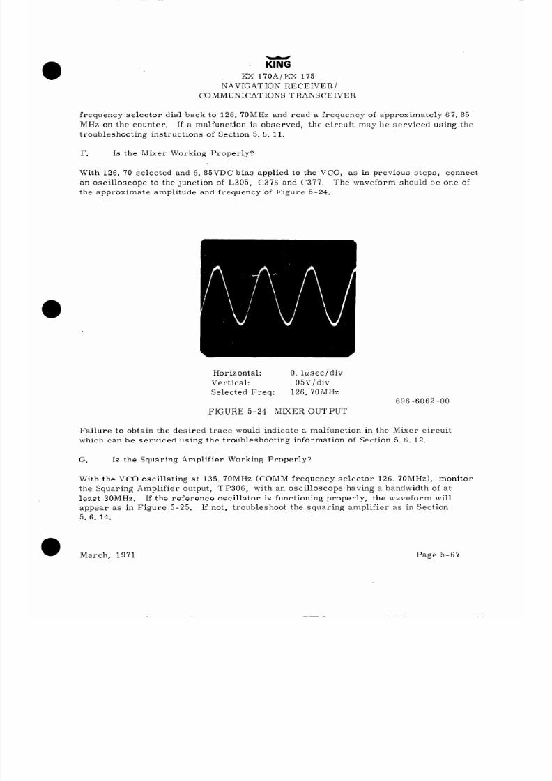
8/9/2019 KX 170A - Maintenance Manual Honeywell
http://slidepdf.com/reader/full/kx-170a-maintenance-manual-honeywell 161/586
KING
KX 170A/KX 175
NAVIGATION RECEIVER/
COMMUNICATIONS TRANSCEIVER
frequency selector dial back to 126. 70MHz and read a frequency of approximately 67. 85
MHz on the counter. If a malfunction is observed, the circuit may be serviced using the
troubleshooting instructions of Section 5. 6. 11.
F.
Is the Mixer Work ing Properly?
With 126. 70 selected and 6. 85VDC bias applied to the VCO, as in previous steps, connect
an oscilloscope to the junction of L305, C376 and C377. The waveform should be one of
the approximate amplitude and frequency of Figure 5-24.
Horizontal: 0. lpsec/div
Vertical: . OSV/div
Selected Freq:
126. 70MHz
FIGURE 5-24 MIXER OUTPUT
696 -6062 -00
Failure to obtain the desired trace would indicate a malfunction in the Mixer circuit
which can be serviced using the troubleshooting information of Section 5. 6. 12.
G.
Is the Squaring Amplifier Work ing Properly?
With the VCO oscillating at 135. 70MHz (COMM frequency selector 126. 70MHz), monitor
the Squaring Amplifier output,
TP306, with an oscilloscope having a bandwidth of at
least 30MHz.
If the reference oscillator is functioning properly, the waveform will
appear as in Figure 5-25, If not, troubleshoot the squaring amplifier as in Section
5. 6. 14.
March, 1971
Page 5-67

8/9/2019 KX 170A - Maintenance Manual Honeywell
http://slidepdf.com/reader/full/kx-170a-maintenance-manual-honeywell 162/586
KING
Kx 170A/KX 175,
NAVIGATION RECEIVER/
COMMUNICATIONS TRANSCEIVER
0
Horizontal: 0. lpsec/div
Vertical: lV/div
Selected Freq. : 126. 70MHz
696 -6063-00
FIGURE 5-25 SQUARING AMPLIFIER OUTPUT
H.
Does the Programmable Divider provide proper frequency division?
Short together test points TP307, TP308 and TP309.
This disables the phase and fre-
quency compara tor to permit testing of the programmable counter. Maintain the channel
setting and the VCO tuning voltage of steps D through G.
Attach the oscilloscope probe
to the junction point of C384, CR317, R366 and Pin 9 of 1308 to monitor the counter out-
put. The waveform of Figure 5-26 should be obtained. Note the pulse period of 40psec.
Dial the eighteen MHz positions,
leaving the VCO bias unchanged, and look for the count-
er output pulse rate to increase uniformly as lower channel frequencies are dialed.
Return the MHz dial to the 126MHz position and dial through the twenty KHz positions.
Observe a gradual increase in output pulse rate as numbers are dialed from the 0. 95 to
0. 00 using counterclockwise rotation.
If erroneous operation of the Programmable Counter is observed, service the counter
using the procedure outlined in Section 5. 6. 3. Upon completion of the counter checks,
remove the shorting connections from TP307, TP308 and TP309.
Page 5-68 March, 1971
l

8/9/2019 KX 170A - Maintenance Manual Honeywell
http://slidepdf.com/reader/full/kx-170a-maintenance-manual-honeywell 163/586
KING
KX 170A/KX 175
NAVIGATION RECEIVER/
COMMUNICATIONS TRANSCEIVER
- -.
Horizontal:orizontal: 5ysecldivysecldiv
Vertical:ertical: 1.. OV/divV/div
Selected Freq:elected Freq: 126. 7MHz26. 7MHz
69696 -6064- 00
FIGURE 5-26 PROGRAMMABLE DIVIDER OUTPUT
I.
Is the Phase and Frequency Comparator Operational?
Connect the oscilloscope probe to the tie point of Pins 1, 5, and 10 of I308 and R333 to
monitor the Phase and Frequency Comparitor output.
With the COMM channel selector
at 126. 70MHz, vary the VCO bias above and below 6. 85 volts.
The output voltage on the
scope should be dominately high when the VCO bias is low, and low when the VCO bias is
high. Wave forms are illustrated on the “set-reset” output “Q” of the Phase and Freq-
uency Comparator timing diagrams of Figure 5-33.
If a malfunction is noted, trouble-
shoot the circuit as instructed in Section 5. 6. 4.
J.
Does the Voltage Translator Operate Properly?
Repeat the test of Step I but with the oscilloscope probe attached to TP302.
Waveforms
are illustrated in Figure 5-27. Troubleshoot the circuit as required using the infor-
mation given in Section 5. 6. 7,
March, 1971
Page 5-f.9

8/9/2019 KX 170A - Maintenance Manual Honeywell
http://slidepdf.com/reader/full/kx-170a-maintenance-manual-honeywell 164/586
NAVIGATION RECEIVER/
COMMUNICATIONS TRANSCEIVER
(a) VCP frequency and bias voltage high. (b) VCO frequency and bias voltage low.
Horizontal: lOpsec/div
Vertical: 2V/div
Selected Freq:
126. 70MHz
696 -6065-00
.
FIGURE 5-27 VOLTAGE TRANSLATOR
K.
What if no Problems are Observed?
Service the remaining block, the VCO Low Pass Filter.
Compare waveforms with those
of Figure 4-14 and voltage levels of figure 5-51.
Check for continuity.
Page 5-70
March, 1971
l

8/9/2019 KX 170A - Maintenance Manual Honeywell
http://slidepdf.com/reader/full/kx-170a-maintenance-manual-honeywell 165/586
KING
KX 170A/KX 175
NAVIGATION RE CEIVER /
COMMUNICATIONS TRANSCEIVER
5. 6. 3 PROGRAMMABLE DIVIDER (Figure 5-29)
The Programmable Divider consists of integrated circuits, 1301, 1302, 1304, 1306 and
gates A and D in 1303.
Reference material includes the divider theory of Section 4. 2 (c)
and the Timing Diagram of Figure 5-32.
-NOTE-
If the NAV SMO is functioning properly, the
servicing technician has the option of using
comparison techniques in troubleshooting
the COMM SMO.
5. 6. 3. 1
Troubleshooting Procedure.
1.
Test Setup.
A.
Open either end of L305, the Mixer Low Pass Filter choke.
B.
Short Pins TP307, TP308 and TP309 together.
C.
Use a coaxial pigtail to connect an H/P 606A or equivalent, to the tie
point of C376 and C377.
II.
Equipment Adjustments.
A.
Using a frequency counter, set the 606A to a CW frequency of 3. 175MHz.
B.
Adjust the H/P 606ACW level to obtain a crisp square wave (0 volts base
line, 4 volts peak line) at TP306, when viewed by an oscilloscope having
a 30MHz or wider bandwidth.
C.
Dial the COMM channel selection to 126. 70MHz.
If NAV SMO comparison
techniques are to be used, select 116. 70MHz for the NAV channel.
III.
Observations
A.
Use a 30MHz bandwidth (or wider) oscilloscope. Provide external sync
from the leading edge of the pulse appearing at the junction of R366 and
CR31 7.
March, 1971
Page 5-71

8/9/2019 KX 170A - Maintenance Manual Honeywell
http://slidepdf.com/reader/full/kx-170a-maintenance-manual-honeywell 166/586
KING
Kx 170A/KX 175
NAVIGATION RECEIVER/
COMMUNICATIONS TRANSCEIVER .
B. Compare the waveform at Pin 9 of 1308 to the equivalent point in the NAV
SMO or to the timing diagram (See Figure 5-32).
The desired output is a
pulse train with a 2. 5 volt peak level, a 40psec period (25KHz rep. rate),
and 0 volts base line.
C.
If the desired oscilloscope trace was obtained in B, the counter is opera-
tional at 126. 70MHz. Dial 135. 95MHz. With the oscilloscope sync as in
A above, simultaneously monitor TP306 and Pin 9 of 1308.
Note the
relationship of the pulses as the dial is rotated sequentially to the next
lowest channel.
The output pulse should step 1 input pulse increment with
each 5OKHz step in dialing (See Figure 5-28). If the counter meets the
above requirements it is operational.
f = 126. 70MHz f = 126. 65MHz
Vertical: Top-lV/div (TP306)
Bottom-O. 5V/div (Pin 9 of the 1308)
Horizontal: 0.
5psec/div
696
-6066 -00
FIGURE 5-28 PROGRAMMABLE DIVIDER
D.
Failure to meet the requirements of Step B requires a complete check of
the I-C input/output timing as defined in either the timing diagram (Figure
5-32) or an operable COMM or NAV SMO.
E. Failure to meet the requirements of Step C implies a problem with the
preset function of the Programmable Divider. A complete check of the
divider flip-flops immediately preceeding and following the preset enable
pulse (negative pulse on Pin 6 of the 1304). The desired preset states are
defined in Table 4-4, where 0 is ground and 1 is 5 volts and should occur
immediately following the preset enable pulse.
Page 5-72
March, 1971

8/9/2019 KX 170A - Maintenance Manual Honeywell
http://slidepdf.com/reader/full/kx-170a-maintenance-manual-honeywell 167/586
KING
KX 17dA/KX 175
NAVIGATION RECEIVER/
COMMUNICATIONS TRANSCEIVER
F. Replace components and make repairs as necessary to obtain the desired
counter operation.
5. 6.4 PHASE AND FREQUENCY COMPARATOR (Figure 5-29)
The Phase and Frequency Comparator consists of integrated circuits 1305, 1307, 1308,
gates B and C of 1303 and wave shaping networks consisting of C383, C384, CR317, C565,
R366 and R367. Reference information sources include the Phase and Frequency Com-
parator Timing Diagram of Figure 5-33 and the theory of Section 4. 2. 2.
5. 6. 4. 1
A.
B.
C.
D.
E.
- NOTE -
If the NAV SMO is operating properly
it may be used to provide supplementary
information using comparison techniques.
Troubleshooting Procedure
Connect an external power supply to the VCO bias test point, TP301.
Monitor the comparito r output (Pins 1,
5, or 10 of 1308) on an oscilloscope.
Adjust the VCO bias voltage low (less than 6. 85 volts with 126. 70 or
135. 70MHz selected) and look for a high output voltage (around 1. 5 volts).
Refer to Figure 5-33 for the appropriate timing diagram.
Adjust the VCO bias voltage high (greater than 6. 85 volts) and look for a
low output voltage (near ground potential). Refer to Figure 5-33 for the
appropriate timing.
Failure to meet the conditions of Steps C and D requires a systematic com-
parison of the input output relationships appearing in either the Timing
Diagram or the functioning NAV SMO.
1.
Disable the counter hold pulses by shorting test points TP307, TP308,
and TP309, and check the divide by 16 block (1305) for proper divide
by 2, divide by 4, divide by 8 and divide by 16 ripple counter operation.
2.
Check the differentiation networks for proper wave shaping (tie point of
C384, CR317, and R366 and the tie point of C383 and R367.
March, 1971
Page 5-73

8/9/2019 KX 170A - Maintenance Manual Honeywell
http://slidepdf.com/reader/full/kx-170a-maintenance-manual-honeywell 168/586
Kx 170A/KX 175
NAVIGATION RECEIVER/
COMMU.NICATIONS TRANSCEIVER
3. Remove the shorting connections at test point TP307, TP308 and TP309.
Repeat the tests of Steps C and D above. If proper operation is still
not obtained, monitor the gates of the MC817P’s (1307 and 1308)and B
and C of the 1304 for proper input/output operation.
Page 5-74
March, 1971
a
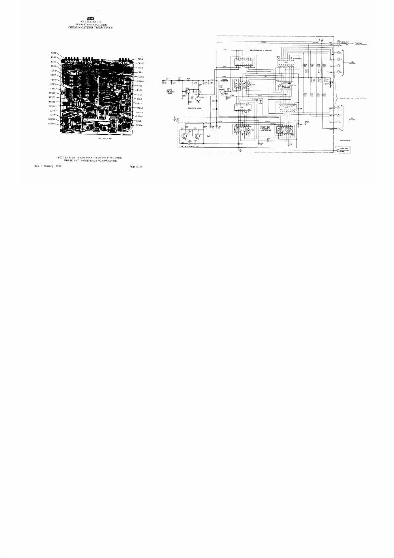
8/9/2019 KX 170A - Maintenance Manual Honeywell
http://slidepdf.com/reader/full/kx-170a-maintenance-manual-honeywell 169/586
KING
KX 17OA/KX 175
NAVIGATION RECEIVER /
COMMUNICATIONS TRANSCEIVER
l 5DC
1 I I
I
P RO GR AM MA BL E D IV D ER
I
I
t308
\
1306\\
1304
\
1302
\
C383\
1307\
-R366
-CR317
-R333
-C384
-TP301
-TP302
-c315
-R367
-c314
-C565
.c317
.CR316
,CR315
TP305
L305
TP304
I305\
MXER
LOW PASS
FILTER
TP308
TP306
TP309
SOUARING AMPL
I
1
+>B”DC
+3”DC
PHASE AND
CJ302
CJ301
,,c- c
“-
w
--y/ ?
696-6067 -00
I
002-0181-R-
I
L LO W- R E FE RE NC E - 0s ~. _ _ _ _ _
I
I
r 1
I
Kltl70. ONLY
J ; 0 4oow1
’
Ih
FROM *” 9YO
(
---------
-----
----------
,
FIGURE 5-29 COMM PROGRAMMABLE DIVIDER/
PHASE AND FREQUENCY COMPARATOR
Rev. 1 January, 1972
Page 5-75

8/9/2019 KX 170A - Maintenance Manual Honeywell
http://slidepdf.com/reader/full/kx-170a-maintenance-manual-honeywell 170/586
m
KX 170A/KX 175
NAVIGATION RECEIVER/
COMMUNICATIONS TRANSCEIVER
5. 6. 5 VOLTAGE CONTROLLED OSCILLATOR (VCO) (Figure 5-30)
The Voltage Controlled Oscillator (VCO) consists of transistor Q302, Varactor diode
CR303, with frequency adjust capacitors C314 and C315 and HI-LO VCO switching
transistor Q301. Diodes CR301 and CR302 disable the VCO transistor Q302 when the
COMM frequency selector wafer is dialed to a nonvalid COMM channel. In the low
portion of the COMM band (118. 00-126. 95MHz), the Hi line is grounded on receive and
the “Lo” line is grounded on transmit. Therefore, in receive the “Hi” line forward
biases CR301 applying bias to Q302 for normal operat,ion. CR302 is reverse biased by
R346 (High Reference Oscillator Section). In the high portion of the COMM band (127. OO-
135. 95MHz) the “Lo” line is grounded on receive and the “Hi” line is grounded on trans-
mit.
Therefore, in receive the “Lo” line, forward biases CR302 which again applies
bias to Q302.
At the same time, the “Lo” line enables VCO switch Q301, placing trim-
mer C314 in parallel with C315. CR301 is reverse biased by R347 (High Reference
Oscillator Section).
5. 6. 5. 1
Troubleshooting Procedure. Check the supply and bias voltages of Q302.
Check for proper operation of the Hi-Lo switching wafer and associated diodes CR301
and CR302.
(See Section 5. 6. 11) Make repairs as necessary to obtain proper operating
conditions. Supply a 7. 0 volt bias voltage from a low impedance source to TP301 and
monitor the VCO output frequency by capacitively coupling a frequency counter to the
collector of Q302 with a 1OOpf diskcap.
With the frequency selector at 126. 95MHz adjust
C315 to get a frequency of approximately 135. 950MHz.
If this is unattainable, verify
that Q301, is turned off and check the frequency determining elements, C317, C387, C315,
C343, L301, and CR303.
Dial 135. 950MHz and adjust C314 to obtain a VCO frequency of
126.950 MHz. If erratic or erroneous operation is noted, check the frequency determin-
ing components and verify that Q301 is saturated.
If the VCO fails to operate, check
L301 and CR303 and Q302. Check the VCO for a proportional change in frequency with
tuning voltage changes on the low and high bands.
5. 6. 6 VCO LOW PASS FILTER (Figure 5-301
The VCO Low Pass Filter consisting of T307, C348, C349, and C350 is an elliptic low
pass filter designed to recover D-C voltage from the output o f the 25KHz Voltage
Translator.
It has been factory adjusted and no attempt should be made to readjust in
the field.
5. 6. 6. 1
Troubleshooting Procedure. Using an oscilloscope, check for a square
wave input at TP302. Using a D-C voltmeter, check for a D-C voltage at TP301 (7. OOV
DC at 126. 95MHz to 2. 58V DC at 118. OOMHz.
March, 1971
Page 5-77

8/9/2019 KX 170A - Maintenance Manual Honeywell
http://slidepdf.com/reader/full/kx-170a-maintenance-manual-honeywell 171/586
KING
KX 170A/KX 175
NAVIGATION RECEIVER/
COMMUNICATIONS TRANSCEIVER
5. 6. 7 25KHz VOLTAGE TRANSLATOR (Figure 5-30)
The Voltage Translator consists of transistors Q308 and Q309 which shift the error
voltage level from the Phase and Frequency Comparator to a level sufficient to operate
the VCO.
5. 6. 7. 1
Troubleshooting
Procedure. Using an
oscilloscope, trace the input
signal
from
pins
1,
5, or 10 of 1308 to the output at TP302.
See Figure 5-51 for typical D-C
operating voltage levels.
5. 6. 8 RECEIVER BUFFER (Figure 5-30)
The Receiver Buffer consists of transistorlQ303 with output transformer T301.
5. 6. 8. 1
Troubleshooting Procedure. Using an oscilloscope, trace the input signal
from R309 to the output at TP303.
See Figure 5-51 for typical D-C operating voltage
levels.
5.6. 9 TRANSMIT SUFFER/TX ENABLE SWITCH/OUT OF LOCK TX DISABLE
The Transmit Buffer consists of Q306 with output transformer T305.
It provides drive
to the transmitter only when both the TX Enable Switch, Q305, is turned off and the
Out of Lock Disable switch Q307 is saturated providing an emitter current.path to ground.
5. 6. 9. 1
Troubleshooting Procedure. Key the transmitter and use an oscilloscope
to track the signal from T301 to Pin 2 of the output transformer T305. Using a D-C
voltmeter,
check the TX enable switch Q305 for proper operation (Saturated in receive,
open in transmit) and check the Out of Lock Disable Q307 for proper operation (satur-
ated-bringing the emitter resistors of Q303 and Q306 to ground.
See Figure 5-51 for
typical D-C operating voltage levels.
Page 5-78
March, 1971
a

8/9/2019 KX 170A - Maintenance Manual Honeywell
http://slidepdf.com/reader/full/kx-170a-maintenance-manual-honeywell 172/586
KING
KX 170A/K-X 175
NAVIGATION RECEIVER/
COMMUNICATIONS TRANSCEIVER
4309
c347
4308
TP302
L301
1308
c343
CR301
CR302
4307
R346
R347
TX. ENABLE SWITCH
I
1 1
vCO/BUFFER
696 -6068 -00
FIGURE 5-30 COMM VOLTAGE CONTROLLED OSCILLATOR/
VCO LOW PASS FILTER/25KHz VOLTAGE TRANSLATOR/
VCO BUFFER/TRANSMIT BUFFER/TRANSMIT ENABLE SWITCH/
OUT-OF-LOCK TRANSMIT DISABLE
Rev. 1 January, 1972
Page 5-79

8/9/2019 KX 170A - Maintenance Manual Honeywell
http://slidepdf.com/reader/full/kx-170a-maintenance-manual-honeywell 173/586
KING
KX 170A/KX 175
NAVIGATION RECEIVER/
COMMUNICATIONS TRANSCEIVER
5. 6. 10 HIGH REFERENCE OSCILLATOR (Figure 5-31)
The High Reference Oscillator consists of transistor Q311 operating in a typical Colpitts
configuration.
Crystals Y301 and Y302 determine the operating frequency.
In the low
portion of the COMM band (118. 00-126. 95MHz), Y301 is used on receive and Y302 is
used on transmit. In the high portion of the COMM band (127. 00-135. 95MHz), Y302 is
used on receive and Y301 on transmit.
5. 6. 10. 1
Troubleshooting Procedure.
Check the oscillator output at Pin 6 of T306.
The following table gives the desired functions under the various conditions encountered.
Low Band (118. 00 - 126. 95MHz)
High Band
(127. 00 - 135. 95MHz)
Receive f = 71. 025MHz Receive f = 66. 525MHz
“Lo” +8. 5V
“Lo” GND
“Hi” GND “Hi” +8. 5V
CR314 Reverse Biased
CR314 Forward Biased
CR313 Forward Biased
C R3 13 Reverse Biased
Transmit f = 66. 525MHz
“Lo” GND
“Hi” +8. 5V
CR3 14 Forward Biased
C R3 13 Reverse Biased
Transmit
f = 71.025MHz
“Lo” +8. 5V
“Hi” GND
CR314 Reverse Biased
C R3 13 Forward Biased
TABLE 5-12 HIGH REFERENCE OSCILLATOR TROUBLESHOOTING TABLE
Check supply and biasing voltages (See Figure 5-51 for typical D-C operating voltage
levels).
5. 6. 11 IMPLICIT DIVIDE BY 2 CIRCUIT (5-31)
The Implicit Divide by 2 circuit consists of balanced mixer CR305, CR306, CR307 and
CR308 and amplifier Q310.
For circuit theory refer to Section 4. 2.
5. 6. 11. 1
Troubleshooting Procedure.
Using an oscilloscope verify output from VCO
Buffer at Pin 6 of T302. Check for signal at the base of Q310 and track through the
amplifier section working toward TP304.
See Figure 5-51 for typical D-C operating
voltage levels. Refer to 5. 5. 12. 1 for procedure for isolating amplifier and mixer
failures.
5. 6. 12 2ND MIXER (Figure 5-31)
This is a balanced mixer consisting of transformers T304 and T306 and diodes CR309,
CR310, CR311 and CR312.
March, 1971
Page 5-81

8/9/2019 KX 170A - Maintenance Manual Honeywell
http://slidepdf.com/reader/full/kx-170a-maintenance-manual-honeywell 174/586
KI G
3
X 170A KX 175
NAVIGATION RECEIVER/
COMMUNICATIONS TRANSCEIVER
5. 6. 12. 1 Troubleshooting Procedure. With the power removed from the KX 170A/
KX 175 using an ohmmeter check all diodes for a possible open. Check all transformer
windings for D - C continuity.
5. 6. 13 MIXER LOW PASS FILTER (Figure 5-31)
The Mixer Low Pass Filter is a basic pi- section low pass filter consisting of inductor
L305 and capacitors C375 and C376.
5. 6. 13. 1
Troubleshooting Procedure.
Using an oscilloscope trace the signal from’
the output of the Second Mixer (Pin 2 of T304) to the input of the Squaring Amplifier
(base of Q312).
5. 6. 14 SQUARING AMPLIFIER (Figure 5-31)
The Squaring Amplifier consists of transistors Q312 and Q313.
5. 6. 14. 1 Troubleshooting Procedure. Using an oscilloscope check for mixer output
signal at the base of Q312. Check TP306 for a 4 volt square wave output.
Check tran-
sistors Q312 and 9313 and associated circuitry (See Figure 5-51 for typical D-C
operating voltage levels).
Page 5-82
March, 1971
a

8/9/2019 KX 170A - Maintenance Manual Honeywell
http://slidepdf.com/reader/full/kx-170a-maintenance-manual-honeywell 175/586
KING
Kx 170A/KX 175
NAVIGATION RECEIVER/
COMMUNICATIONS TRANSCEIVER
+8 ,UC
l . 0 5 VDC
- *
-
WHT
I
I
r
------
- C356
R334
To IYf
100 =
IOY.
t2 AMPL.
FF2-
3000
I
g
C367
^ _-
R346
CR314
R345
5 6K
Y
I BK 10%
I -
y
II
~ ~052255HHt~P
c R3 ’3 p z a T
=
9.E
10%
=
r
I
REFERENCE
I
c371
osc.
= s MH z
T
r
0 Ipf
C361
330
fT302
CR306
.CR305
.CR308
,CR307
,Q310
CR310
CR309
T304
CR312
TP304
-------I
R349
I 5K
0312
MIXER
LOW PASS
FILTER
1352
3 OK
696 -6069 -00
-CR311
SQUARING AMPL.
FIGURE 5-31 COMM HIGH REFERENCE OSCILLATOR/
IMPLICIT-2 CIRCUIT/2ND MIXER/ MIXER LOW PASS
FILTER/SQUARING AMPLIFIER
March, 1971
Page 5

8/9/2019 KX 170A - Maintenance Manual Honeywell
http://slidepdf.com/reader/full/kx-170a-maintenance-manual-honeywell 176/586

8/9/2019 KX 170A - Maintenance Manual Honeywell
http://slidepdf.com/reader/full/kx-170a-maintenance-manual-honeywell 177/586
KING
KX 170A/KX 175
NAVIGATION RECEIVER /
COMMUNICATIONS TRANSCEIVER
+I6
-400KHz REF
MC817P(7) PIN 2
200 KHz
9989 PIN 5
100 KHz
9989 PIN 4
50 KHz
9989 PIN 3
25KHz REF
9989 PIN 2
25KHz REF
RESET INPUT
(MC817P(8) PIN 6
COUNTER OUTPUl
9004 PIN6
COUNTER OUTPUT
SET INPUT
(MC817P(8) PIN91
SET-RESET
OUTPUT a
(MC817P(8) PIN51
VOLTAGE
TRANSLATOR
OUTPUT
(TP302 /202)
LOW PASS
FILTER OUTPUT
(TP301/201)
A) PHASE LOCK
B) VCO FREQUENCY HIGH
C) VCO FREQUENCY LOW
APPROXIMATE WAVEFORMS
(COUNTER FREQ. LOW)
(COUNTER FREQ. HIGH 1
- 125.00,134.00, I 16.00 MHz
-l2l.O0 , 130.00, Il2.00MHz
----
-- _------
----
I I
I
1 I 1
11 I/II
xfDFS,RED <
II- I.
I-J l-----:Irr~Lu
-
iI II
PHASE ESTABLISHED TO GIVE PROPER
VCO BIAS TO MAINTAIN PHASE LOCK
ill
3Volts
DC DRIVES fVCO TO -MAINTAIN
Ref.
DC DRIVES fVC0 LOW
Ref.
DC DRIVES fVCO HIGH
696-6071-00
PHASE LOCK
FIGURE 5-33 TIMING DIAGRAM PHASE AND FREQUENCY COMPARATOR
March, 1971
Page 5-87

8/9/2019 KX 170A - Maintenance Manual Honeywell
http://slidepdf.com/reader/full/kx-170a-maintenance-manual-honeywell 178/586
NAVIGATION RE CEIVER /
COMMUNICATIONS TRANSCEIVER
5.7 TROUBLESHOOTINGHENAVRECEIVER
Receiver schematic diagram Figure 5-52.
5. 7. 1 PRELIMINARY EVALUATION (Isolating the malfunction by stage gain measure-
merits)
a.
At some convenient channel frequency apply a 10~~ RF signal modulated
30% by a 1 KHz audio signal.
b.
Connect an oscilloscope to the detector TP403 and determine that the out-
put is approximately 1. 7 volts peak-to -peak. If
processing, (go to step f). If not, the failure is
the detector (go to step cl.
so the failure is in audio
between the R-F input
and
C.
Determine if the failure is within the AGC AMP.
Connect a variable
voltage power supply to TP412 through a 1KR resistor.
Compare the
input voltage to output voltage relationship with the typical data of Figure
5-34.
0
TP406
t-
OUTPUT VOLTAGE
I N PUT VOLTS
696-6072 -00
FIGURE 5-34 AGC AMP D-C CHARACTERISTICS
If reasonable correlation is obtained, disconnect the power supply and
proceed to step d. If not, repair the AGC amplifier.
March, 1971
Page 5-89

8/9/2019 KX 170A - Maintenance Manual Honeywell
http://slidepdf.com/reader/full/kx-170a-maintenance-manual-honeywell 179/586
KING
KX 170A/KX 175
NAVIGATION RECEIVER/ -
COMMUNICATIONS TRANSCEIVER
I
d. Check the detector for .proper operation. Connect TP412 to ground, dis-
abling the AGC Amp.
Apply 4. OVdc to AGC test point TP406 to provide
receiver quieting.
Inject a. 7Vrms 1. 1857MHz signal having 300/o, 1KHz
amplitude modulation to the base of detector transistor Q404 as shown
(Figure 5-35).
696 -6073 -00
FIGURE 5435 DETECTOR TEST SETUP
Using an oscilloscope at the detector
collector (TP403) ther’e should be
approximately 3. 5Vdc with a 2. OV peak to peak signal superimposed.
If
this result is not obtained repair the detector refer,ing to the discussion of
5. 7. 8. If the detector operation appears normal, continue to step e.
Page 5-90
March, 1971
a
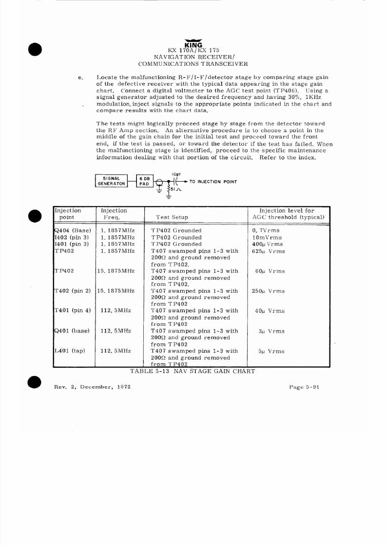
8/9/2019 KX 170A - Maintenance Manual Honeywell
http://slidepdf.com/reader/full/kx-170a-maintenance-manual-honeywell 180/586
KING
KX l’IOA/KX 175
NAVIGATION RECEIVER/
COMMUNICATIONS TRANSCEIVER
e.
Locate the malfunctioning R-F/I-F/detector stage by comparing stage gain
of the defective receiver with the typical data appearing in the stage gain
chart.
Connect a digital voltmeter to the AGC test point (TP406). Using a
signal generator adjusted to the desired frequency and having 3070, 1KHz
modulation, inject signals to the appropriate points indicated in the chart and
compare results with the chart data.
The tests might logically proceed stage by stage from the detector toward
the RF Amp section.
An alternative procedure is to choose a point in the
middle of the gain chain for the initial test and proceed toward the front
end, if the test is passed, or toward the detector if the test has failed. When
the malfunctioning stage is identified, proceed to the specific maintenance
information dealing with that portion of the circuit. Refer to the index.
njection
point
Injection
Freq.
Test Setup
Injection level for
AGC threshold (typical)
2404 (Base)
l. 1857MHz
T P402 Grounded
0, 7Vrms
402 (pin 3)
1. 1857MHz TP402 Grounded
10mVrms
401 (pin 3)
1. 1857MHz TP402 Grounded
400~ Vrms
‘P402
1. 1857MHz
T407 swamped pins l-3 with
625~ Vrms
2000 and ground removed
from TP402.
‘P402
15. 1875MHz
T407 swamped pins l-3 with
60~ Vrms
200R and ground removed
from TP402.
‘402 (pin 2) 15. 1875MHz T407 swamped pins l-3 with 250~ Vrms
2OOfi and ground removed
from TP402
‘401 (pin 4)
112. 5MHz
T407 swamped pins l-3 with
40~ Vrms
2000 and ground removed
from TP402
2401 (base) 112. 5MHz T407 swamped pins l-3 with 3~ Vrms
2OOs2 and ground removed
from TP402
,401 (tap)
112. 5MHz
T407 swamped pins l-3 with
5~ Vrms
200R and ground removed
from TP402
PA T - II l c) nrnrr C-rr-Ann ,- nrnr mTTAnm
Rev. 2, December, 1972
Page 5-91
8/9/2019 KX 170A - Maintenance Manual Honeywell
http://slidepdf.com/reader/full/kx-170a-maintenance-manual-honeywell 181/586
KX 170A/KX 175
NAVIGATION RE,CEIVER /
COMMUNICATIONS TRANSCEIVER.
f.
Trace the audio signal through the audio processing network to locate the
malfunctioning stage. Refer to 5. 7. 8.
Page 5-92
March, 1971
a

8/9/2019 KX 170A - Maintenance Manual Honeywell
http://slidepdf.com/reader/full/kx-170a-maintenance-manual-honeywell 182/586
KING
KX 170A/KX 175
NAVIGATION RECEIVER/
COMMUNICATIONS TRANSCEIVER
RED T U N NG V OLT A GE
f
I
NAV. PRESELECTOR RF AMPL.
L402
3 3yh
62K
R403 5%
IK
5%
BALANCED
MIXER
15.1875MHr , 1st IF
1403
r-----
1
--_--_
X 1700. ONLY
2 nd MIXER
d
L 0 . F R OM N AV S M O
c41
TP
T4
%
T4
c4
T4
CR
CR
CR
CR
T4
L40
c4
CR
c4
%
c4
L4
CR
L4
CR
c4
L4
696 -6074
-00
FIGURE 5-36 NAV PRESELECTOR/RF AMPLIFIER/lST MIXER/ST I. 1;.
Rev. 1 January, 1972
8/9/2019 KX 170A - Maintenance Manual Honeywell
http://slidepdf.com/reader/full/kx-170a-maintenance-manual-honeywell 183/586
KX 170A/KX 175
NAVIGATION RECEIVER/
COMMUNICATIONS TRANSCEIVER
.
5. 7, 2 PRESELECTOR/RF AMPLIFIER (Figure 5-36)
The NAV preselector is a three pole filter,
consisting of three variable inductors L401,
L403 and L405 in conjunction with varactors CR401, CR402 and CR403 and fixed capac-
itors C401, C407 and C414.
The varactors are tuned by a voltage supplied from the
NAV SMO.
-.
Txe-ga-in of RF Amplifier Q401, is reduced by applying an increasing, positive AGC
voltage to thebase.
--..
5. 7. 2. 1
Troubleshooting Procedure.
Check for correct tuning voltage. (See tuning
voltage chart, Section 5. 2. 3 Table 5-3. ) Check for RF signal at base of Q401. If no
signal appears at Q401, check for RF signal at the input coaxial cable and the top of
L403.
Check coupling inductor L402 and capacitor C408.
If signal appears at the base
of Q401, check for RF signal at the top of L405.
If no signal appears, check RF Amp-
lifier Q,401, coupling capacitor C411 and associated circuitry (See Figure 5-32 for
operating voltage levels).
5. 7. 3 1ST MIXER (Figure 5-36)
The balanced mixer consists of T401, T402 and CR404 through CR407.
The R-F signal
is connected to pin 4 of T401 and the synthesizer injection to pin 4 of T402.
The IF
signal appears on pin 2 of T402.
5. 7. 3. 1
Troubleshooting Procedure.
Check frequency and amplitude of NAV SMO
Local Oscillator injection at pin 4 of T402.
(Point X of Figure 5-4). Check for the
presence of the RF Signal at pin 4 of T401 (after removing Local Oscillator coaxial
cable).
If both of the above checks prove satisfactory,
check continuity of transformer
windings and diodes CR404 - CR407.
5. 7. 4 1ST I-F (Figure 5-36)
The first 1-I‘ consists of a four pole crystal filter (KX 175/KX 175B only) or 2 pole
crystal filter (KX 170A/KX 170B only).
Capacitors C415 and C417 provide matching to
the first and second mixers respectively.
Transformers T403 and T404 provide proper
reactive terminations to the filter.
5. 7. 4. 1
Troubleshooting Procedure. Remove the 2nd Local Oscillator injection from
Q403 by lifting one lead of Local Oscillator coupling capacitor C418. Check for signal
(15. 1875MHz) at the base of the second mixer (TP402). If no signal is present, check
each filter component.
Rev. 2, December, 1972 Page 5-95
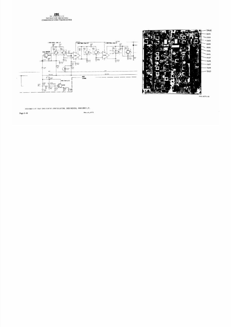
8/9/2019 KX 170A - Maintenance Manual Honeywell
http://slidepdf.com/reader/full/kx-170a-maintenance-manual-honeywell 184/586
KX 17%‘p,%X 175
NAVIGATION RECEIVER/
COMMUNICATIONS TRANSCEIVER
1.1857MHr 2nd IF
R409
c419
+a 5VDC
+a SVDC
1.1857MHz 2nd
IF
T 1.1857Ml-l~ 2nd
IF
c424
C428
CR410
-
C4lb
.a2
AGC
I==
e5VDC
~-
i
C425
To IYf
=
---
+
T
C436
_ 0 Id
R421
IOK
AGC
’
0
r C44R
,.
33
NAV 2nd L.O.
NAV.
-GiiiK-
696-6075-00
FIGURE 5-37 NAV 2ND LOCAL OSCILLATOR, 2ND MMER, AND 2ND I. F.
March, 1971

8/9/2019 KX 170A - Maintenance Manual Honeywell
http://slidepdf.com/reader/full/kx-170a-maintenance-manual-honeywell 185/586
iG
Kx 170A/KX 175
NAVIGATION RE CEIVER /
COMMUNICATIONS TRANSCEIVER
5. 7. 5 2ND LOCAL OSCILLATOR (L. 0. ) (Figure 5-37)
The second Local Oscillator consists of a transistor Q408 operating as a Pierce oscillator
with crystal, Y401, determining its operating frequency (14. 0018MHz).
5. 7. 5. 1
Troubleshooting Procedure. Check for proper injection signal at TP402
(400mv peak-to-peak) and if possible,
measure frequency with a counter. Check coup-
ling capacitor, C418. If no injection,
check Q408 and associated circuitry (See Figure
5-52 for operating voltage level).
5. 7. 6 2ND MIXER (Figure 5-37)
The second mixer consists of a transistor, Q403, to which both the R-F signal and the
Local Oscillator injection are coupled into the base.
5. 7. 6. 1 Troubleshooting
Procedure. If both the 1st
I-F
signal (See Section
5. 7. 4. 1
and Local Oscillator injection (See Section 5. 7. 5. 1) are present at TP402, and if they
are of the correct frequency (IF = 15. 1875MHz, LO = 14. 0018MHz) check Q408 and
circuitry (See Figure 5-52 for operating voltage levels).
5. 7. 7 2ND I-F (Figure 5-37)
The second I-F consists of three pairs of double tuned filters T405-T406, T407-T408,
T409-T410, with I-C Amplifiers 1401 and 1402 providing selectivity and I-F gain, AGC
voltage is applied to 1401.
The second I-F is tuned to 1. 1857MHz.
Refer to section
4. 4. 2. 8 for AGC theory.
5. 7. 7. 1
Troubleshooting Procedure.
Check for proper second I-F signal at Pin 2 of
each I-F transformer, starting with T405 and working towards T410.
If no R-F signal
is found at any of the above points,
check the associated circuitry between that point
and the last point at which a signal was observed.
(For operating voltage levels, see
Figure 5-52. )
March, 1971
Page 5-99

8/9/2019 KX 170A - Maintenance Manual Honeywell
http://slidepdf.com/reader/full/kx-170a-maintenance-manual-honeywell 186/586
w ’
KING
KX 170A/KX 175
NAVIGATION RECEIVER /
COMMUNICATIONS TRANSCEIVER
+ a 5 VD C
1 T
1
R422
47K
5 %
32r
2 4K
5%
CR411
R429
IOK
&
c439
.22”f ,
2ov
:E1412
c440
IO”1
AMPL.
ISOLATION
a407
I
AGC
TP406
COMM.
AM
----
-1
I
I
26
+E SVDC
I\ 0
I
YEL/GRh
VOR/LOC OUT
SPARE
t444
50
NAV AUDIO AMPL.
TO
FRONT
WNEL
I.
FIGURE 5-38 NAV DETECTOR/NO ISE LIMITER, AGC AMPLIFIER,
IDENT FILTER, AND AUDIO AMPLIFIER
Rev. 1, January, 1972
8/9/2019 KX 170A - Maintenance Manual Honeywell
http://slidepdf.com/reader/full/kx-170a-maintenance-manual-honeywell 187/586
iTi%
KX 170A/KX 175
NAVIGATION RECEIVER/
COMMUNICATIONS TRANSCEIVER
5. 7.8 DETECTO R/NOISE LIMITER (Figure 5-38)
The detector consists of transistor Q404 which is operated in the collector detection
mode by the trickle bias supplied by CR410.
Isolation amplifier Q405 is an emitter
follower which prevents the noise limiter from loading the detector. For a detailed
description of the noise limiter see paragraph 4. 3. 2. 6.
5. 7. 8. 1 Troubleshooting Procedure.
Check the detected signal at TP403. If no
signal is present, check for I-F signal at Pin 2 of T410.
Further, check transistor
Q4O4 and associated circuitry (See Figure 5-52 for operating voltage levels).
For the noise limiter, first check the emitter of Q405 for a detected audio signal.
Using
an oscilloscope, check the audio at the junction of CR411 and C439.
If no audio exists,
check CR411 for an open or reverse biased condition.
(See Figure 5-52 for operating
voltage levels).
5. 7. 9 AGC AMPLIFIER (Figure 5-38)
The output of the isolation amplifier is filtered (and phase shifted) by the filter network
R431, C444, R432 and C441 and applied to the base of AGC amplifier Q406. Q406 com-
pares this voltage with the AGC threshold reference appearing at the junction of RT502
and R434 and amplifies the difference voltage in conjunction with Q407.
5. 7. 9. 1
Troubleshooting Procedure.
An inoperative AGC system can best be check-
ed by comparing the D-C operating voltage levels of the AGC circuitry.
These operat-
ing voltage levels are shown in Figure 5-52.
For a motorboating AGC system,check capacitors C441 and C442 for either a capacitance
change or an open circuit to the capacitor.
5. 7. 10 IDENT FILTER (Figure 5-38)
The NAV Ident Filter consists of a parallel L-C trap using fixed capacitor, C716 and a
variable inductor L703 to tune the filter to 1020Hz. A switch, Slll located on the trans-
ceiver front panel disables the ident filter by directly shorting across the L-C network
when in-the “Ident” position.
5. 7. 10. 1
Troubleshooting Procedure.
Check for proper operation of switch Slll by
placing an ohmmeter across L703 and switching Slll back and forth between “Voice” and
“Ident” positions.
With the switch in “Voice” position,
Sill should be open and the ohm-
meter should read the resistance of L703 which is approximately 25 ohms.
If the ohm-
meter reads open or high, L703 is open.
If the ohmmeter reads close to zero ohms,
Sill is not opening in the “Voice” position.
With Slll in “Ident” position, the ohmmeter
should read zero ohms.
Check for proper alignment of L703 by modulating the Signal
March, 1971
Page 5-103

8/9/2019 KX 170A - Maintenance Manual Honeywell
http://slidepdf.com/reader/full/kx-170a-maintenance-manual-honeywell 188/586
KING
KX 170A/KX 175
NAVIGATION RECEIVER/
COMMUNICATIONS TRANSCEIVER
Generator with a variable frequency audio generator.
As the audio frequency range is
scanned, a definite dip should be observed in the audio output at the resonate frequency
of the filter.
The dip should be observed in the audio output at the resonate frequency
of the filter.
If the dip is slightly removed from 1020Hz (use a counter to measure the
audio frequency if available) realignment may be necessary.
If no dip is observed and
the above tests have proven satisfactory,
check C716 for an open circuit or an incorrect
value.
5. 7. 11 AUDIO AMPLIFIER (Figure 5-38)
The NAV Audio Amplifier consists of a decoupled-regulated supply voltage (Zener diode
CR414), I-F audio amp 1403, and output transformer T411.
The NAV Audio Volume
Control, RlOl, is located on the transceiver front panel.
5. 7. 11. 1 Troubleshooting Procedure.
Check the D-C operating voltage levels of the
Audio Amplifier 1403 (See Figure 5-52). If the D-C levels are OK, trace the audio from
the ident filter thru the NAV Volume Control RlOl (NAV Volume Control should be all
the way clockwise) to Pin 10 of 1403.
To check transformer T411, with an oscilloscope
look at Pins 4 and 7 of 1403 to see if a signal exists. If so, and it does not appear at
Pin 35 of 5171, check T411 for an open secondary winding or the yellow-orange wire for
an open circuit.
Page 5-104
March, 1971
a

8/9/2019 KX 170A - Maintenance Manual Honeywell
http://slidepdf.com/reader/full/kx-170a-maintenance-manual-honeywell 189/586
zix
KX 170A/KX 175
NAVIGATION RECEIVER/
COMMUNICATIONS TRANSCEIVER
5.8 TROUBLESHOOTINGHECOMMRECEIVER
Receiver schematic diagram Figure 5-52.
5. 8. 1 PRELIMINARY EVALUATION (Isolating the malfunction by stage gain measure-
ments).
a.
At some convenient channel frequency,
apply a 10~~ RF signal modulated
30% by a 1KHz audio signal.
b. Connect an oscilloscope to the detector TP410 and determine that the output
is approximately 1. 0 volts peak-to-peak.
If so the failure is in audio pro-
1 cessing (go to step f). If not the failure is between the R-F input and the
detector (go to step c).
C.
Determine if the failure is within the AGC AMPL. Connect a variable volt-
age power supply to TP413 through a 1Kn resistor. Compare the input
voltage to output voltage relationship with the typical data of Figure 5-39.
POWER
SUPPLY
2.4-3.7VDC
INPUT VOLTAGE
TP411
OUTPUT
VOLTAGE
INPUT VOLTAGE
696 -6077 -00
FIGURE 5-39 AGC AMPL. D-C CHARACTERISTICS
If reasonable correlation-is obtained, disconnect the power supply and proceed to step
d.
If not, repair the AGC amplifier.
March, 1971
Page 5-105

8/9/2019 KX 170A - Maintenance Manual Honeywell
http://slidepdf.com/reader/full/kx-170a-maintenance-manual-honeywell 190/586
KING
KX 170A/KX 175
NAVIGATION RECEIVER/
COMMUNICATIONS TRANSCEIVER
d.
Check the detector for proper operation.
Connect T P4 13 to ground,. dis-
abling the AGC AMPL. Apply 4. OVdc to AGC test point TP411 to provide
receiver quieting.
Inject a O.$Vrms, 861. 25 KHz signal having 300/o, 1KHz
amplitude modulation as shown to the base of detector transistor Q414 as
shown. (Figure 5-40).
I
Page 5-106
Rev. 2, December, 1972
l
FIGURE 5-40 DETECTOR TES
696-6078-00
1T SETUP
l
sing an oscilloscope at the detector collector,(TP410) should be approx-
i
imately 2. 5Vdc with a 1. OV peak to peak signal superimposed.
If this result -
is not obtained repair the detector refering to the discussion of 5. 8. 8.
If the
detector operation appears normal, continue to step e.

8/9/2019 KX 170A - Maintenance Manual Honeywell
http://slidepdf.com/reader/full/kx-170a-maintenance-manual-honeywell 191/586
-
KX 17K0’AN/%X 175
NAVIGATION RECEIVER/
COMMUNICATIONS TRANSCEIVER
e.
Locate the malfunctioning R-F/I-F/detector stage by comparing stage gain
of the defective receiver with the typical data appearing in the stage gain
chart. Connect a digital voltmeter to the AGC test point (TP411).
Using
a signal generator adjusted to the desired frequency and having 300/o, 1KHz
modulation,inject signals to the appropriate points indicated in the chart
and compare results with the chart data.
The tests might logically proceed stage by stage from the detector toward
the RF AMPL. section. An alternative procedure is to choose a point in the
middle of the gain chain for the initial test and proceed toward the front
end, if the test is passed, or toward the detector if the test has failed.
When the malfunctioning stage is identified, proceed to the specific main-
tenance information dealing with that portion of the circuit.
Refer to the
index.
Injection
Injection
point Freq.
Test Setup
2414(base) 861. 25KHz TP409 Grounded
I405(pin 3) 861. 25KHz
TP409 Grounded
I404(pin 3) 861. 25KHz
TP409 Grounded
rp409 861. 25KHz
T418 swamped pins l-3 with 20052
and ground removed from TP409
r P409
9. OOMHz T418 swamped pins l-3 with 200R
and ground removed from TP409
I413(pin 2)
9. OOMHz T418 swamped pins l-3 with 2000
and ground removed from TP409
I412(pin 4) 126. 50MHz
T418 swamped pins l-3 with 2OO iZ
and ground removed from TP409
2411(base) 126. 50MHz
T418 swamped pins l-3 with 200R
and ground removed from TP409
L407(tap) 126. 50MHz
T418 swamped pins l-3 with 2000
and ground removed from TP409
Injection level for
AGC threshold (typical
0. 6Vrms
9mVrms
250yVrms
400pVrms
30pVrms
1 OOpVrms
40pVrms
20pVrms
15pVrms
TABLE 5-14 COMM STAGE GAIN CHART
Rev. 2, December, 1972
Page 5-107

8/9/2019 KX 170A - Maintenance Manual Honeywell
http://slidepdf.com/reader/full/kx-170a-maintenance-manual-honeywell 192/586
KING
KX 170A/KX 175
NAVIGATION RECEIVER/
COMMUNICATIONS TRANSCEIVER
f. Trace the audio signal through the audio processing network to locate the
malfunctioning stage. Refer to 5. 8. 8.
Page 51108
March, 1971
a

8/9/2019 KX 170A - Maintenance Manual Honeywell
http://slidepdf.com/reader/full/kx-170a-maintenance-manual-honeywell 193/586
ia
KX 170A/KX 175
NAVIGATION RECEIVER/
COMMUNICATIONS TRANSCEIVER
---
-------
L4l2
c47.a 1
150
IpL
\I
I
c468
L407
c469
CR41
CR41
L408
L409
c475
c474
%i
L411
L412
CR41
CR41
C481
L413
CR42
T412
CR42
CR42
T413
CR42
C482
T414
C467
FL403
T415
4413
-TP40
-C483
-
696 -6079 -00
COMM PRESELECTOR, R. F. AMPLIFIER, 1ST MIXER, AND 1ST I. F.
5-110
Rev.
1 January, 1972

8/9/2019 KX 170A - Maintenance Manual Honeywell
http://slidepdf.com/reader/full/kx-170a-maintenance-manual-honeywell 194/586
KING
KX 170A/KX 175
NAVIGATION RECEIVER/
COMMUNICATIONS TRANSCEIVER
5. 8. 2 PRESELECTOR/RF AMPLIFIER (Figure 5-41)
The COMM preselector is a four pole filter,
consisting of four variable inductors L407,
L409, L411 and L413 in conjunction with varactor CR416, CR417, CR418, CR419 and
fixed capacitors C469, C474, and C481.
The varactors are tuned by a tuning voltage
obtained from a COMM MHz tuning wafer (S102).
The R-F Amplifier Q411 provides RF gain which is reduced by an increasing AGC volt-
age to the base,
5. 8. 2. 1
Troubleshooting Procedure.
Check for correct tuning voltage (See tuning
voltage chart Section 5. 2. 3).
Check for R-F signal at base of Q411. If no signal appears,
check for R-F signal at the input coaxial cable and the top of L407 and L409.
Check
coupling elements C468, L408 and C475. If signal appears at Q411 base, check for
R-F signal at the top of L411 and L413.
If no signal appears at the top of L411, check
the R-F amplifier, Q411, coupling components C478 and L412 and associated circuitry
(See Figure 5-52 for operating voltage levels).
5. 8. 3 1ST MIXER (Figure 5-41)
Balanced mixer components include T412,
T413, and CR420 through CR423. The R-F
signal is connected to pin 4 of T412 while the COMM SMO receiver injection is applied
to pin 4 of T413.
The resultant 1st IF signal appears on pin 2 of T413.
5. 8. 3. 1
Troubleshooting Procedure.
Check frequency and amplitude of COMM SMO
L. 0. injection at pin 4 of T413 (Point Y of Figure 5-4).
Check for the presence of the
R-F signal at pin 4 of T412 (after removing L. 0. injection coaxial cable).
If both of the
above checks prove satisfactory,
check for continuity of transformer windings and diodes
CR420-423.
5. 8.4 1ST I-F (Figure 5-41)
The first I-F consists of a two pole crystal filter (.KX 170A/KX 175/KX 170B only) or a
six pole crystal filter (KX 175B only) tuned to 9.OOOOMHz.
(T414, T415 and FL403 or
FL405, FL406 and FL407, KX 175B only).
5.8.4. 1
Troubleshooting Procedure.
Remove the second L. 0. injection from Q413
by lifting one lead of L. 0. coupling capacitor C467.
Check for R-F signal (9. OOOOMHz)
at the base of the second mixer (TP409). If no signal is present, check each filter
component associated coupling capacitors C482 and C483.
Rev. 2, December, 1972
Page 5-111

8/9/2019 KX 170A - Maintenance Manual Honeywell
http://slidepdf.com/reader/full/kx-170a-maintenance-manual-honeywell 195/586
KING
KX 170A/KX 175
NAVIGATION RECEIVER/
COMMUNICATIONS TRANSCEIVER
5. 8. 5 2ND LOCAL OSCILLATOR (Figure 5-42)
The second L. 0. consists of a transistor Q409 operating as a Pierce Oscillator with
crystal Y402 determining its operating frequency (8. 13875MHz).
5. 8. 5. 1 Troubleshooting Procedure.
Check for proper injection signal and measure
frequency with a counter. Check coupling capacitor C467. If no injection, check Q409
and associated circuitry (See Figure 5-52 for operating voltage levels).
5. 8. 6 2ND MIXER (Figure 5-42)
The second mixer consists of a transistor, Q413, to which both the R-F signal and the
L. 0. inje’ction are coupled into the base.
5. 8. 6. 1 Troubleshooting Procedure. If both the 1st I-F signal (see Section 5. 8. 4)
and the L. 0. injection (see Section 5. 8. 5) are present at TP409 and if they are of the
correct frequency, (IF=9. OOOMHz, L. 0. = 8. 1375MHz) ch,eck Q413 and circuitry (see
Figure 5-52 for operating voltage levels).
5. 8. 7 2ND I-F (Figure 5-42)
The second I-F consists of three pairs of double tuned filters T416-T417, T418-T419,
T420-T421, with I-C amplifiers 1404 and 1405 providing selectivity and I-F gain. AGC
voltage is applied to 1404. The second I-F is tuned to 861. 25KHz. Refer to section
4. 3. 2. 7 for ‘AGC theory.
5. 8. 7. 1 Troubleshooting Procedure. Check for proper second I-F signal at Pin 2
of each I-F transformer, starting with T4 16 and working towards T421. If no I-F signal
is found at any of the above points, check the associated circuitry between that point
and the last point at which a signal was observed (For operating voltage levels,
see
Figure 5-52.
Page 5-112
March, 1971

8/9/2019 KX 170A - Maintenance Manual Honeywell
http://slidepdf.com/reader/full/kx-170a-maintenance-manual-honeywell 196/586
KING
KX 170A/KX 175
NAVIGATION RECEIVER/
COMMUNICATIONS TRANSCEIVER
-T421
-T420
-1405
-T419
-T418
'1404
sY402
'T417
4409
T414
T416
C467
4413
TP409
W’
R455
? r
100
ia 51
T
2.0
1456
,u 47
+B.SVDC
861.25KHz 2nd IF c481
6.3
861.25KHt 2nd IF
L4
I
$6
98
24
FIGURE 5-42 COMM 2ND L. 0.. 2ND MIXER, 2ND I. F., AND DETECTOR
(Dwg. No. 696-6080-00)
Rev. 2,
December,
1972
Page
5-113

8/9/2019 KX 170A - Maintenance Manual Honeywell
http://slidepdf.com/reader/full/kx-170a-maintenance-manual-honeywell 197/586
KING
KX 170A/KX 175
NAVIGATION RECEIVER/
COMMUNICATIONS TRANSCEIVER
+8 5VDL
DETECTOR .~~a(3
0414 -
-4
+ 3 5VDC
CRNGRY
F RO M C 0f w . + .9 W DC R E G
AOC
I
+R SVDC
CSll
%
CR431U
tI/ WHTBLU
WI07 I
g Y$f
~SOUELCH GATE
I\
T O C OM M V OL UM E C ON TR OL
IOU
5 %
u
WI-IT/VI0
CR430.’
TO SOUELCH TEST SWITCH
AUDIO 4MPL
M L C DN TR OL
WHT/ORN
C465
Q410
C466
c499
CR426
WHT BLU
T421
CR42 7
4414
TP410
R487
Q416
R485
Q415
c495
R486
GRY WHT
c497 ’
FIGT;,J
5-43 NAV DETECTOR/NOISE LIMITER/
AGC AMPLIFIER/AUDIO PREAMPLIFIER
(Dwg. No. 696-608 l-00)
Page 5-116
Rev. 2, December, 1972

8/9/2019 KX 170A - Maintenance Manual Honeywell
http://slidepdf.com/reader/full/kx-170a-maintenance-manual-honeywell 198/586
KING
KX 170A/KX 175
NAVIGAT ION RECEIVER /
COMMUNICATIONS TRANSCEIVER
5; 8. 8 DETECTOR/NOISE LIMITER (Figure 5-43)
The detector consists of transistor Q414 which is operated in the collector detection mode
by the trickle bias supplied by CR426.
For a detailed description of the noise limiter see
paragraph 4. 3. 2. 6.
5. 8. 8. 1
Troubleshooting Procedure.
Check for detected signal at TP410.
If no
signal is present, check for I-F signal at Pin 2 of T421.
Further, check transistor
Q414 and associated circuitry.
(See Figure 5-52 for operating voltage levels)
For noise limiter operation, first check TP410 for a detected audio signal.
Using an
oscilloscope, check the audio at the junction of CR427 and C499.
If no audio exists,
check CR427 for an open or reverse biased condition.
(See Figure 5-52 for operating
voltage levels).
5. 8. 9 AGC AMPLIFIER (Figure 5-43)
The detector output is filtered by the filter network R487 and C495 and applied to the base
of AGC amplifier Q415. Q415 compares this voltage with the AGC threshold reference
appearing at the junction of R485 and R486 and the voltage difference controls AGC
transistor Q4 16.
5. 8. 9. 1
Troubleshooting Procedure.
An inoperative AGC system can best be
checked by comparing the D-C operating voltage levels of the AGC circuitry Q415, Q416,
R487, R485, and R486. These operating voltage levels are shown in Figure 5-52.
For a motorboating AGC system, check capacitors C495 and C497 for either a cap-
acitance change or an open circuit to the capacitor.
5. 8. 10 AUDIO PREAMPLIFIER (Figure 5-43)
The COMM audio preamplifier consists of transistor Q410 operating as a Class A Audio
stage. The COMM Audio Volume Control R102 is located on the transceiver front panel.
5. 8. 10. 1 Troubleshooting Procedure. Check for audio existing at the white-blue
wire going to the COMM Volume Control.
If no audio is present, refer to paragraph
5. 8. 11 for the squelch gate troubleshooting procedure.
If audio is present, check for
audio at the coax returning from the volume control (make sure volume control
is all the way clockwise-full volume).
If no audio is present check the volume control
for continuity (10K from white-blue wire to ground).
If audio is present at the volume control coax but not on the white-orange
audio out line, check coupling capacitors C466 and (‘465.
If audio exists at the base o f
Q410 but not the collector,
check Q410 and associated circuitry.
(See Figure 5-52 for
operating voltage levels. )
March, 1971
Page 5-117
8/9/2019 KX 170A - Maintenance Manual Honeywell
http://slidepdf.com/reader/full/kx-170a-maintenance-manual-honeywell 199/586
KING
KX 170A/KX 175
NAVIGATION RECEIVER/
COMMUNICATIONS TRANSCEIVER
5. 8. 11 SQUELCH GATE (Figure 5-44)
The basic squelch gate consists of gating diode CR43i and squelch reference network
R508 and R509.
As long as CR431 is forward biased (i. e., The cathode is dropped to
a lower D-C potential than the anode squelch reference voltage), the diode acts as an
A-C short circuit and audio passes from the noise limiter, through C499, CR431 and
C511 to the COMM Volume Control. If CR431 is reverse biased (i. e., The cathode vol
age is held at a lower positive D-C potential than the anode squelch reference voltage),
the diode acts as an A-C open circuit and no audio is allowed to pass.
Under normal operation, there are three conditions which will give an unsquelched
receiver; the squelch test switch in test position,
carrier to noise squelch gating and
carrier squelch gating.
t-
5. 8. 11. 1
Troubleshooting Procedure.
The squelch gate is most easily checked by
determining what is or is not allowing CR431 to become forward biased.
If the re-
ceiver remains unsquelched with no signal,
check CR431 for a shorted condition, check
the squelch test switch S109 for proper open circuit condition in “on” position, check
the carrier to noise squelch for proper operation,
(see paragraph 5. 8. 13. 1 and check
carrier squelch for proper operation, (see paragraph 5. 8. 14. 1).
If the receiver re-
mains squelched with signal applied, check CR431, R506 and R507 for an open
condition,
and check the carrier to noise and carrier squelch circuits for proper
operation (see above for appropriate paragraphs).
5. 8. 12 NOISE AMPLIFIER AND FILTER (Figure 5-44)
‘J‘he noise amplifier and filter consist of the noise amplifier Q419 and the elliptic filter
formed by C503, (“502, (J501,
1,414, 11500 and the input impedance of Q419. The filter
rejects frequencies below 7Kl-Iz and the amplifier is used to amplify the filtered noise
at)ove this frequency,
5. 8. 12. 1
Troubleshooting Procedure. With no signal input to the receiver, check
for amplified (clipped-square wave) noise at the collector of Q419.
If no noise exists
(but is present at TP410), check ttle carrier/noise squelch adjust pot R483 for an open
condition,
check the filter network I’or open components, and check Q419 and associated
circuitry (See Figure 5-52 for operating voltage levels).
5. 8. 13 CARRIER TO NOISE SQUI:lLt’tI (ta‘igure 5-44)
The carrier to noise squelch consists of transistor Q420 and C‘R429 in conjunction with
capacitor C508.
For a detailed description of operation see Section 4. 3. 2. 9.
The basic
operation is that with no signal input,
noise is amplified in transistor Q420, and a volt-
age is developed across C508 which biases squelch gate (‘R431 off.
With an input signal,
noise is reduced and the voltage developed across C508 drops allowing CR431 to become
forward biased.
March, 1971
Page 5-119

8/9/2019 KX 170A - Maintenance Manual Honeywell
http://slidepdf.com/reader/full/kx-170a-maintenance-manual-honeywell 200/586
iti%
Kx 17OA/KX 175
NAVIGATION RECEIVER /
COMMUNICATIONS TRANSCEIVER
5. 8. 13. 1 Troubleshooting Procedure. With no signal applied to the receiver input,
check for a D-C voltage of approximately 7. 5V across C508.
If ther,e is no D-C or if it
is much lower than 7. 5V, check Q420 and all associated circuitry (See Figure 5-52 for
operating voltage levels).
5. 8. 14 CARRIER SQUELCH (Figure 5-44)
The carrier squelch consists of the differential amplifier pair Q417 and Q418.
Its prin-
ciple operation is to compare the AGC voltage with a preset carrier squelch reference
voltage (Potentiometer R495). ‘When the AGC.voltage becomes greater than this ref-
erence voltage, Q418 turns on and forward biases squelch gate diode CR431.
5. 8. 14. 1 Troubleshooting Procedure. Check the voltage reference string R494, R495
and R496 for continuity. Check for differential amplifier operation of Q417 and Q418.
When an R-F signal is applied to the receiver (above 151.l~ hard) the AGC voltage on the
base of Q418 should turn it on pulling its collector voltage down and allowing Squelch
Gate diode CR431 to turn on.
For ‘approximate D-C operating levels, refer to Figure
5-52. It should be noted there that the given D-C operating voltage levels for the
carrier squelch are only approximate as they are dependent upon the quiescent AGC
level and will vary between units.
They are given for comparison purpose only.
Page 5-1‘20
March, 1971

8/9/2019 KX 170A - Maintenance Manual Honeywell
http://slidepdf.com/reader/full/kx-170a-maintenance-manual-honeywell 201/586
'R496
R483
R495
R500
c501
TP410
R494
c503
L414
c502
4419
4420
/CR429
-c499
-C508
-RR507
-R506
-CR431
-R509
-R508
-cc511
NOISE
FILTER
KING
KX 170A/KX 175
NAVIGATION RECEIVER/
COMMUNICATIONS TRANSCEIVER
* '.""I
35v
CARRIER I NOISE
CW CARRIER
CARRIER _ ~OUELCH
T O CO MM
TO SOUEL
696-6082-
FIGURE 5-44 COMM SQUELCH GATE, NOISE AMPLIFIER AND FI
CARRIER TO NOISE SQUELCH AND CARRIER SQUELCH
March, 1971

8/9/2019 KX 170A - Maintenance Manual Honeywell
http://slidepdf.com/reader/full/kx-170a-maintenance-manual-honeywell 202/586
Kxlldhrb175
NAVIGATION RECEIVER/
COMMUNICATIONS TRANSCEIVER
5.9 TRDUBLESHOOTINGHEAUDIO MPL
(Schematic Diagram Figure 5-53)
5. 9. 1 SUMMING JUNCTION (Figure 5-45)
The summing junction consists of resistor network R703 thru R707 and
R722. Besides
a COMM receiver audio input,
it provides up to four external auxilary inputs with approx-
imately 30db of isolation between any two of the external inputs (6OOn).
5. 9. 1. 1
Troubleshooting Procedure.
A direct approach using either an ohmmeter
to check for open resistors and open or shorted paths or an audio oscillator to inject a
1KHz tone into each input port with an oscilloscope to check for the tone is recommended.
Check C704 for proper input coupling.
5. 9. 2 T-R DIODE SWITCH (Figure 5-45)
The T-R Diode switch consists of switching diodes CR701 and CR702 along with associa-
ted bias circuitry.
For receive condition, the audio mute line is open eliminating any
D-C current path to CR701.
This, in effect reverse biases CR701 and forward biasing
CR702.
For transmit operations the audio mute line is grounded by K701 allowing CR701 to be-
come forward biased thru R701 and R721,
This pulls the anode of CR702 low causing it
to become reverse biased.
Thus, summing junction audio is blocked while the mike
audio line is coupled thru C714, CR701 and C705 into the Audio Pre-Driver Amplifier
Q701.
5. 9. 2. 1 Troubleshooting Procedure.
Check the reference voltage developed be-
tween R708 and R710.
Alternately ground audio mute line (white-grey) and check bias-
ing of diodes CR701 and CR702. For D-C operating voltages under both transmit and
receive conditions, see Figure 5-53.
Check for open or shorted diodes CR701 and
CR702 and check coupling capacitor C705.
5. 9. 3 AUDIO PRE-DRIVER AMPLIFIER (Figure 5-45)
The Audio Pre-Driver Amplifier, Q701 operates as a Class A audio stage.
It is used in
both the transmit and receive modes.
March, 1971
Page 5-123

8/9/2019 KX 170A - Maintenance Manual Honeywell
http://slidepdf.com/reader/full/kx-170a-maintenance-manual-honeywell 203/586
NAVIGATION RECEIVER/
COMMUNICATIONS TRANSCEIVER
5. 9. 3. 1
Troubleshooting Procedure.
Check the coupling capacitors C705 and C706
for proper operation.
If audio appears on the base o f Q701 but does not appear on the
collector, check Q701 and associated circuitry (See Figure 5-53 for operating voltage
levels ). .’
5. 9.4 AUDIO DRIVER AMPLIFIER (Figure 5-45)
The Audio Driver Amplifier Q702 operates as a Class A audio stage having coupling
transformer T701 as its output load.
Distortion is reduced and gain stabilized with the
use of feedback network R718, R713 and C715.
5. 9.4. 1
Troubleshooting Procedure.
Check coupling transformer for an open
winding (no D-C on collector of Q702).
If audio appears on the base of Q702 but not on
the collector, check Q702 and associated circuitry (See Figure 5-53 for operating
voltage levels).
5. 9. 5 ,AUDIO OUTPUT AMPLIFIER (Figure 5-53)
The Audio Output Amplifier consists of T701, T702 and Q703-Q706.
It operates as a
conventional transformer coupled Class B Push-Pull Output Stage. It is used for rec-
eiver audio output and as a modulator for the transmitter.
5. 9. 5. 1
Troubleshooting Procedure.
Check fuse F701 to make sure it has not blown.
The output circuits receive their supply voltage through this fuse. Check transformers
T701 and T702 (open windings - no D-C voltages). Check Q703-Q706 for proper oper-
ation. (See Figure 5-53 for operating voltage levels. )
Page 5-124
March, 1971
a

8/9/2019 KX 170A - Maintenance Manual Honeywell
http://slidepdf.com/reader/full/kx-170a-maintenance-manual-honeywell 204/586
KX 170A/KX 175
NAVIGATION RECEIVER/
COMMUNICATIONS TRANSCEIVER
c7
c709-
C706-
R7
-R721
R702
-R726
,706
‘20
R706
R707
R704
R703' /
I
\ \R710
R705
R727
F701
“,F’
r
~-~-~------~~~-
J171
R707
1 AUDIO
I OUTPUT
AMPL
T-R DIODE
SWITCH
Al
PI
AMPL.
FROM VOLT
REG. DIODE @ wHT + OVDc
+B.OVDC
JUNCTON
R702
c R707
‘ /It
F7Ol CR70T
5A
I
I
A
R721
2 2K
I
A UCO MUTE (WHT GRY
I I
( MIC. AUDIO (GRYI
MC KEY L RYWHT
1
39
40
C OM M S W B US S w n 1
17
C OM M A K B US S ( RE DI
70
_NAV. 13.75VDC INPUT IrEL)
NAV 13.75VDC (YELWHT
- ‘~~~
NOT USED IN KY 195
Imh - 21
=
I
-
1 _ UEPwnT
L702
26
-
C713
250P”
6ROyf
y 25v
FIGURE 5-45 SUMMING JUNCTION, T-R DIODE SWITCH,
AUDIO PRE-DRIVER, AUDIO DRIVER, AUDIO OUTPUT AMPLIFIER
(Dwg. No. 696 -608 3 -00)
Rev. 2, December, 1972 Page 5-125
8/9/2019 KX 170A - Maintenance Manual Honeywell
http://slidepdf.com/reader/full/kx-170a-maintenance-manual-honeywell 205/586
m
KX 17OA/KX 175
NAVIGATION RECEIVER/
COMMUNICATIONS TRANSCEIVER
5.10 TROUBl.ESHOOTINGHETRANSMITTER
(Schematic Diagram Figure 5-53)
5. 10. 1 BUFFER AMPLIFIER (Figure 5-46)
The Buffer Amplifier, Q601, operates as a Class A R-F amplifier.
It receives its R-F
drive from the COMM SMO but is active only in the transmit mode when 13. 75V is sup-
plied to its collector thru relay K701, and the COMM SMO Transmit Buffer (Q306) is
activated.
5. 10. 1. 1 Troubleshooting Procedure.
Check for R-F excitation from the COMM
SMO at the coaxial cable input.
Using a high frequency oscilloscope (being careful not
to load the circuit) check for an R-F signal on the base of QSOl.
Check for R-F signal
at the collector of &Sol. If no signal is present, check Q601 and associated circuitry
(see Figure 5-53 for operating voltage levels).
5. 10. 2 PRE-DRIVER AMPLIFIER (Figure 5-46)
The Pre-Driver Amplifier Q602 is also operated as a Class A, R-F amplifier.
It is
also active only in the transmit mode since it receives its 13. 75V supply voltage as
does Q601 - thru the transmit relay K701.
5. 10. 2. 1 Troubleshooting Procedure.
Check for R-F drive from Q601. If an R-F
signal is present on the base of Q602, but not on the collector, check Q602 and associat-
ed circuitry (See Figure 5-53 for operating voltage levels).
5. 10. 3 DRIVER AMPLIFIER (Figure 5-46)
The Driver Amplifier, Q603, is operated as a Class A-B, R-F Amplifier. It is coll-
ector modulated, receiving a modulated supply voltage thru K701. The resistor and
Liiode combinations CR601-R608 and CR602-R615 are chosen to linearize modulation by
allowing full upward modulation but limiting the downward modulation of Q603.
5. 10. 3. 1 Troubleshooting Procedure.
Check for R-F drive from Q602. If an R-F
signal is present at the base o f Q603 but not at the collector,
check Q603 and its associa-
ted circuitry (See Figure 5-53 for D-C operating voltage levels).
If no modulation occurs
on the collector, check the modulated supply voltage from K701 for proper modulation
level, check resistor-diode combinations (R608-CR601 and R615-CR6021 for open cir-
cuits short circuits or incorrect component value.
March, 1971
Page 5-127

8/9/2019 KX 170A - Maintenance Manual Honeywell
http://slidepdf.com/reader/full/kx-170a-maintenance-manual-honeywell 206/586
KING
Kx 17OA/KX 175
NAVIGAT ION
RE CEIVE R /
COMMUNICATIONS TRANSCEIVER
5. 10.4 FINAL AMPLIFIER (Figure 5-46)
The Final Amplifier Q604 is operated as a Class C R-F amplifier.
It is also collector
modulated, receiving its modulated supply voltage thru K701 in the transmit mode only.
It receives both upward and downward modulation.
5. 10. 4. 1
Troubleshooting Procedure.
Check for R-F drive from Q603. If an R-F
signal is present at the base of Q604 but not the collector,
check Q604 and its associated
circuitry (See Figure 5-53 for D-C operating voltage levels).
If no modulation occurs
on the collector of Q604, check the modulated supply voltage from K701 for proper mod-
ulation level.
5.10. 5 LOW PASS FILTER/T-R DIODE SWITCHING (Figure 5-46)
The Low Pass Filter is a 3-section elliptical filter designed to reduce the harmonic out-
put of the power amplifier.
The T-‘R Diode Switching is accomplished with diodes CR603
and CR.604.
In the receive mode, a positive bias voltage is applied to diodes CR603 and.
CR604 thru resistors R616 and R6 17.
The received signal is coupled from the antenna
thru the 3rd pole and diode CR604, to the COMM receiver.
Diode CR603 and R-F by-
pass capacitor C626 provide a terminating device to minimize the insertion loss.
In the transmit mode, the D-C bias voltage is removed from the resistor, diode com-
bination by relay K701 and the R-F power from the transmitter reverse biases diodes
CR603 and CR604 due to self-rectification.
5. 10. 5. 1
Troubleshooting Procedure. With power removed, check all resistive
(R616 and R617) and all inductive (L604, FL601, FL602 and FL603) components for D-C
continuity (all inductive components should read approximately zero ohms),
In the
receive mode, check for proper forward biasing of diodes CR603 and CR604.
In the
transmit mode, check to see if the bias voltage is removed from CR603 and CR604.
Page 5-128
March, 1971
a
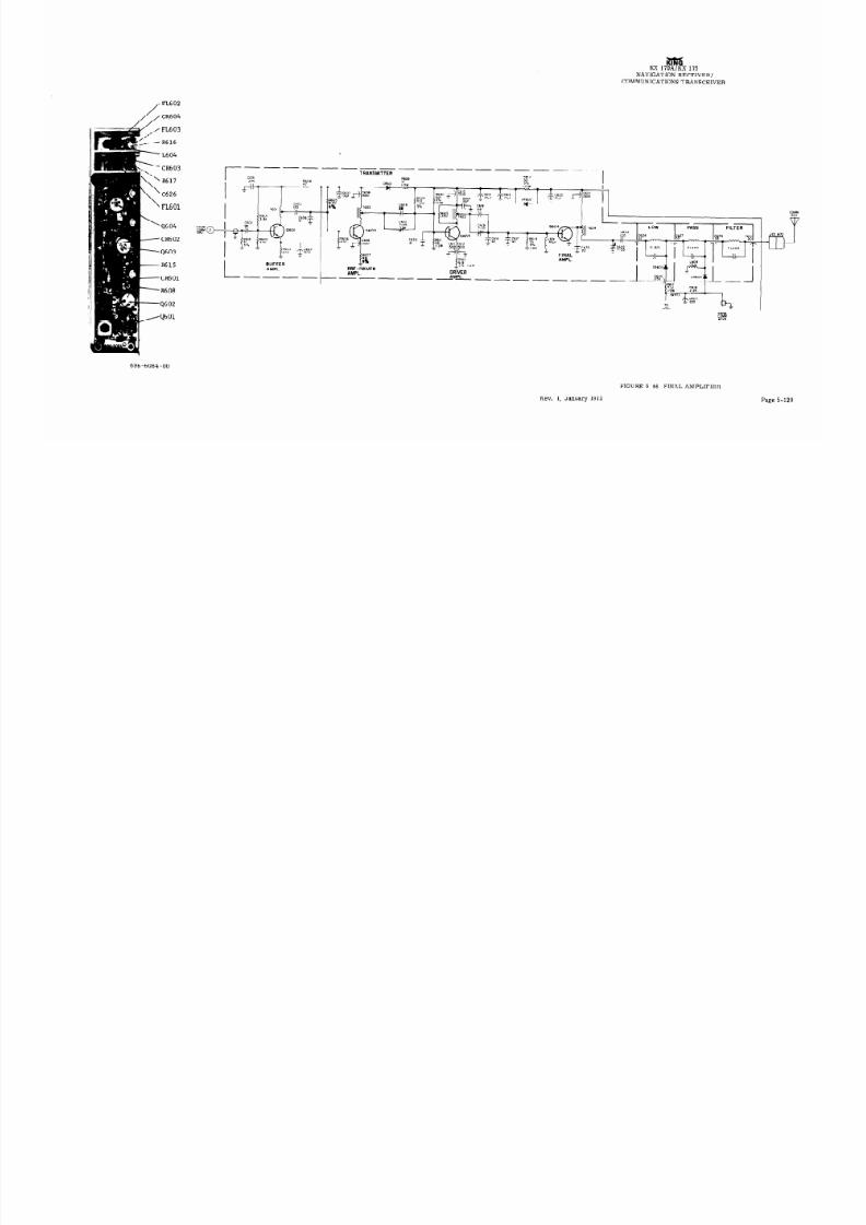
8/9/2019 KX 170A - Maintenance Manual Honeywell
http://slidepdf.com/reader/full/kx-170a-maintenance-manual-honeywell 207/586
KING
KX 170A/KX 175
NAVIGATION RECEIVER/
COMMUNICATIONS TRANSCEIVER
FL602
CR604
R617
C626
FL601
4604
CR602
4603
R615
CR601
R608
4602
4601
TRANSMITTER
C601
470
R604
i
R601
3 9K
2
t ”
1 i
Rg?
,
47K
5 %
=
BUFFER
AMPL.
L--P-
PRE-DRIVER
AMPL.
R612
68
5% ll2W
:
DRIVER
AMPL.
---
y 1-
C632
FINAL
33
AMPL.
-
------
I22 - _ I33
7‘
CT\
I
CR603~~
C626
696 -6084 -00
FIGURE 5-46 FINAL AMPLIFIER
Rev.
1, January 1972
Page 5

8/9/2019 KX 170A - Maintenance Manual Honeywell
http://slidepdf.com/reader/full/kx-170a-maintenance-manual-honeywell 208/586
PI03
l-cl-l
AV +8.5VDC REL
GRY
49 TO NAV. REC NAV. SMO.
-’ TPUT
305 FOR G 5. SWITCHING
WC
WHT
TO AU[llCl BOARU AND
?(I NAV SMO 400 K C. OX
696 -6085-00
KING
KX 170A/KX 175
NAVIGATION RECEIVER/
COMMUNICATIONS TRANSCEIVER
CR102.
NAV +8.51
Q103-
QlOl.
NAV +13.75-
R130-
COMM+8.5-
R132-
Q104-
COMM
CR103=
R131
Rl25;
4102,
4105,
+13.75
T;IG IJRE 5-4 7 REGIJLATORS
March, 1971
age 5-132

8/9/2019 KX 170A - Maintenance Manual Honeywell
http://slidepdf.com/reader/full/kx-170a-maintenance-manual-honeywell 209/586
KING
KX 170A/a 175
NAVIGATION RECEIVER/
COMMUNICATIONS TRANSCEIVER
5.11 TROUBLESHOOTINGHEREGULATORS
5. 11. 1 COMM 8. 5 VOLT REGULATOR (Figures 5-47 and 5-54)
A complementary configuration using two transistors (QlO2 and Q105) as a series pass
element was selected to enhance low supply voltage operation.
Transistor Q104 provides
negative feedback to the base of Q105.
5. 11. 1. 1
Troubleshooting Procedure.
If no output, check for 13. 75V input on orange-
white wire.
If 13. 75V is present, disconnect the orange-grey wires (3 total) and the
white (2 wires).
Check the collector of Q102 for 8 . 5V.
If this has corrected the pro-
blem, replace wires one at a time to isolate the shorted assembly.
Erroneous or
erratic adjustment, necessitates checking R130-R132, CR103 and R125.
If output is high (13. 75V), check for shorted transistor QlO2, Q105 or an open conn-
ection to Q104.
5. 11. 2 8. 5V NAV REGULATOR (Figure 5-47 and 5-54)
The 8. 5v NAV regulator is a conventional series regulator consisting of a series control
transistor pair QlOl and Q103 and reference element CR102.
5. 11. 2. 1 Troubleshooting Procedure. If no output, check for 13. 75V input on yellow/
white wire. If 13. 75V is present, disconnect the grey (3 total) wires, and white (2 total)
wires, and check the collector of QlOl for 8. 5V.
If this has corrected the problem,
replace wires one at a time to isolate the shorted assembly. Check the voltage at zener
diode CR102 (approximately 9. 1V).
If output is high, check for shorted transistor QlOl or Q103 or open connection on
zoner CR102.
March, 1971
Page 5-133
8/9/2019 KX 170A - Maintenance Manual Honeywell
http://slidepdf.com/reader/full/kx-170a-maintenance-manual-honeywell 210/586
KING
Kx 170A/KX 175
NAVIGATION RECEIVER/
COMMUNICATIONS TRANSCEIVER
5.12 TROUBLESHOOTINGHEWA 9 VOLTAGEEGULATOR (Figure 5- 56)
The KA 39 Voltage Converter contains dual series regulators converting 27. 5Vdc to
13. 75Vdc. The COMM regulator, “A”,
incorporates reference element CR101 and the
Darlington series pass configuration consisting of QlOl and Q102.
Protection from
reverse voltage connections and negative transients is provided by diode CR102.
Capacitor Cl01 suppresses spurious oscillations which might otherwise appear with
reactive loads.
The NAV regulator,
“B” functions electrically in the same manner as
the “A” regulator.
5. 12. 1 Troubleshooting Procedure. Compare actual operating voltage with those
specified in Figure 5-56. Low voltage could be caused by a shorted output, a shorted
zener reference diode, an open zener diode bias resistor (R102”A”orR103 “B”), an
open collector resistor (RlOl “A” or R104 “B”), or an open series pass transistor.
Conversely, a high voltage could result from shorted series pass transistors, a shorted
capacitor (Cl01 or C102) an open zener diode,
a shorted zener diode bias resistor (R102
or R103) or an out of tolerance zener diode.
Page 5-134
March, 1971
a

8/9/2019 KX 170A - Maintenance Manual Honeywell
http://slidepdf.com/reader/full/kx-170a-maintenance-manual-honeywell 211/586
KING
Kx 170A/KX 175
NAVIGATION RECEIVER /
COMMUNICATIONS TRANSCEIVER
DME
VO+?/LOC
- G S. CONTWX
I PROGdd%ABLEtl - - -
M
2 POLE
r
.1857M-b
: TO
corn
.SM
t
t
F.'. .. .'
25KHr --.
:
.“cD 1 :. D-c-. . :. ,. : .‘. -. .“.
VOLTAGE
vco
-----c
vco -
..
-i’-
TRANSLATOR .-
: ., BUFFER
:
il. _ :. --_
,-- OiEk-LOOP
,
-TEST POINT
/ . ..-.
-.
::
IVE
TUNING VOLTAGE
92 6125-
1
102 7625MHz
I
I
I NAV AUD
CRYSTAL
I---
ILTER
15.1675MHz
14 OOl8MHz
1
696-6006-00
A/C -,/ 13.75VDC
HASH
6.5VDC
BUSS
- FILTER - REGULATOR
FIGURE 5-48 NAV BLOCK DIAGRAM
March, 1971
Page 5-135

8/9/2019 KX 170A - Maintenance Manual Honeywell
http://slidepdf.com/reader/full/kx-170a-maintenance-manual-honeywell 212/586
KING
KX 170A/KX 175
NAVIGATION RECEIVER/
COMMUNICATIONS TRANSCEIVER
1
1 1
vA~,RAc;~ “ARACTOR
BALANCED
l R F AM P
I IST MX -
XTAL
F LTER - 2 d MX
2 P OL E
- F LTER - F LTER
l IF A MP
( 2 P OL E,
(2 POLEI
SMHZ 86125KHZ
t
t
t
t I
I
I
A
2 POLE
FILTER
sM.*5KH*
.
1.F AMPLOW PASS -
POWERMP
SPEAKER
SIDETONE
RESISTOR tOPTK)NAL)
ON
SPEAKER
A”CKJ
XMIT KEY -
HEADPHONE,
SIDETONE
L
696-6087-00
INPUTS
FIGURE 5-49 COMM BLOCK DIAGRAM
March, 1971
Page 5-137

8/9/2019 KX 170A - Maintenance Manual Honeywell
http://slidepdf.com/reader/full/kx-170a-maintenance-manual-honeywell 213/586

8/9/2019 KX 170A - Maintenance Manual Honeywell
http://slidepdf.com/reader/full/kx-170a-maintenance-manual-honeywell 214/586

8/9/2019 KX 170A - Maintenance Manual Honeywell
http://slidepdf.com/reader/full/kx-170a-maintenance-manual-honeywell 215/586

8/9/2019 KX 170A - Maintenance Manual Honeywell
http://slidepdf.com/reader/full/kx-170a-maintenance-manual-honeywell 216/586

8/9/2019 KX 170A - Maintenance Manual Honeywell
http://slidepdf.com/reader/full/kx-170a-maintenance-manual-honeywell 217/586

8/9/2019 KX 170A - Maintenance Manual Honeywell
http://slidepdf.com/reader/full/kx-170a-maintenance-manual-honeywell 218/586

8/9/2019 KX 170A - Maintenance Manual Honeywell
http://slidepdf.com/reader/full/kx-170a-maintenance-manual-honeywell 219/586

8/9/2019 KX 170A - Maintenance Manual Honeywell
http://slidepdf.com/reader/full/kx-170a-maintenance-manual-honeywell 220/586

8/9/2019 KX 170A - Maintenance Manual Honeywell
http://slidepdf.com/reader/full/kx-170a-maintenance-manual-honeywell 221/586

8/9/2019 KX 170A - Maintenance Manual Honeywell
http://slidepdf.com/reader/full/kx-170a-maintenance-manual-honeywell 222/586

8/9/2019 KX 170A - Maintenance Manual Honeywell
http://slidepdf.com/reader/full/kx-170a-maintenance-manual-honeywell 223/586

8/9/2019 KX 170A - Maintenance Manual Honeywell
http://slidepdf.com/reader/full/kx-170a-maintenance-manual-honeywell 224/586

8/9/2019 KX 170A - Maintenance Manual Honeywell
http://slidepdf.com/reader/full/kx-170a-maintenance-manual-honeywell 225/586

8/9/2019 KX 170A - Maintenance Manual Honeywell
http://slidepdf.com/reader/full/kx-170a-maintenance-manual-honeywell 226/586

8/9/2019 KX 170A - Maintenance Manual Honeywell
http://slidepdf.com/reader/full/kx-170a-maintenance-manual-honeywell 227/586

8/9/2019 KX 170A - Maintenance Manual Honeywell
http://slidepdf.com/reader/full/kx-170a-maintenance-manual-honeywell 228/586

8/9/2019 KX 170A - Maintenance Manual Honeywell
http://slidepdf.com/reader/full/kx-170a-maintenance-manual-honeywell 229/586
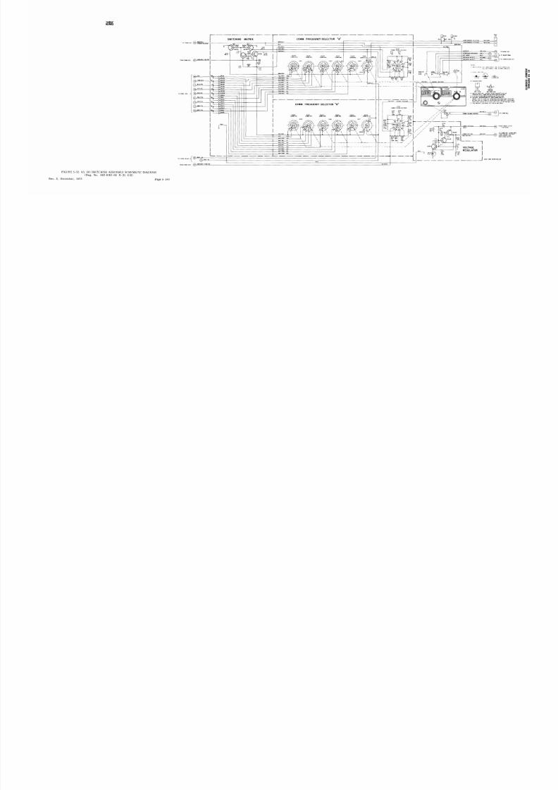
8/9/2019 KX 170A - Maintenance Manual Honeywell
http://slidepdf.com/reader/full/kx-170a-maintenance-manual-honeywell 230/586

8/9/2019 KX 170A - Maintenance Manual Honeywell
http://slidepdf.com/reader/full/kx-170a-maintenance-manual-honeywell 231/586

8/9/2019 KX 170A - Maintenance Manual Honeywell
http://slidepdf.com/reader/full/kx-170a-maintenance-manual-honeywell 232/586
I
CYCLE
14.25
14.0
I
I
KA-39 CONVERTER
I- m e - - - -I
NOTE:
002-0162-00 (R-2)
CONVERTER “A” VOLTAGES:
ABOVE LINE -
RCVR AS LOAD, NO AUDIO.
BELOW LINE -
TRANSMIT CONDITION AS LOAD, NO MODULATION .
FIGURE 5-56 KA 39 VOLTAGE CONVERTER SCHEMATIC DIAGRAM
March, 1971
Page 5-151

8/9/2019 KX 170A - Maintenance Manual Honeywell
http://slidepdf.com/reader/full/kx-170a-maintenance-manual-honeywell 233/586
ASSEMBLY NO. 069-1016-00
DESCRIPTION KX175
LJNIT KX175
PAGE 1
REVISION 14
USED ON ASSEMBLY 069-1016-00
ASSEMBLY DRAWING NO. 300-0419-00
SYMBOL PART NUMBER
DESCRIPTION OUANTI TY
006-0057-00
008-0004-00
008-0005-03
012-1006-00
016-1015-00
016-1038-00
035-101 l-00
035-1013-04
Rl 035-1031-00
047-1728-01
047-1729-01
047-1730-02
047-1731-02
047-1737-0.1
Rl 047-1747-00
047-1943-00
047-2267-02
047-2268-01
047-2269-01
047-2293-01
Rl 047-2327-01
057-1210-00
057-1344-01
076-0339-00
089-2105-22
089-2140-00
R1 089-5878-04
R1 089-5878-13
089-5899-04
089-5903-04
089-6008-03
089-6008-04
089-6167-05
089-6258-04
091-0118-03
091-OllR-04
091-0118-05
150-0020-10
187-1011-00
200-0082-00
200-0249-00
200-0250-00
200-0251-00
200-0252-00
IK MANUAL
LUG GROUND #4
LUG GROUND
TAPE COATED LACING
ADHESIVE
SPRAY ADHESIVE
END CAP SHIPPING
SHIPPING BAG PLAST
SHIPPING CARTON
COMM COVER
COVER PA
LEFT SIDE RAIL
RIGHT SIDE RAIL
NAV COVER
TOP CDVER
CLIP SPRING
COVER BOTTOM
SHIELD PA@ (MIXER)
SHIELD PAD (OSCJ
SHIELD PAD
COVER EOlJIPMENT
PATENT LABEL
SERIAL NLJMBER TAG
SPACER
NUT SPEED NO 4
NUT ESNA f14
SCR PPH 4-40X1/4
SCR PHP 4-40X13/16
SCR PPH 2 56X1/4
SCR PPH 4-40X1/4
SCR PFH 4 40X3/16
SCR PFH 4-40X1/4
SCR FHP 6-32X5/16
SCR PFH 4-24X1/4
INSULATOR
INSIJLATDR
FISHPAPER
TUBING TEF CLR 18
C INER RlJBRER
REAR PLATE ASSY
NAV/COMM BOARD SA
REAR DIVIDER SA
COMM SMO SA
NAV SMO SA
SWITCH HEAD SA
1
1
2
2
1
1
1
1
1
1
1
1
1
1
2
1
1
1
1
1
6
8
2
2
7
4
7
10
12
4
8
2
1
1
.2
2
1
1
1
1
1
1
00-0253-00
.JOTE: R indicates revision,
See page 6-2A for revision and new parts.
Rev. 2, December, 1972
Page 6-l

8/9/2019 KX 170A - Maintenance Manual Honeywell
http://slidepdf.com/reader/full/kx-170a-maintenance-manual-honeywell 234/586
ASSEMBLY NO. 069-1016-00
DESCRIPTION KX175
IJNIT KX175
REVISION 14
USED ON ASSEMBLY 069-1016-00
ASSEMBLY DRAWING ,NO. 300-0419-00
SYMBOL
PART NIJMBER
DESCRIPTION
200-0254-00
FRONT PLATE SA
200-0255-00
CONN CABLE SA
PAGE 2
a
QUANTI TY
1
1
Page 6-2
Rev. 2, December,1972

8/9/2019 KX 170A - Maintenance Manual Honeywell
http://slidepdf.com/reader/full/kx-170a-maintenance-manual-honeywell 235/586
Parts List Revision Record
Assembly No: 069-1016-00
Manual Revision 1
ACTION
SYMBOL
PART NUMBER
DESCRIPTION QUANTITY
ADDED 006-5053-00
Maintenance Manual
1
CHANGE 035-1031-01
Shipping Carton
1
CHANGE 047-2338-01
Top Cover
1
CHANGE 047-1695-00
Cover Equipment
1
CHANGE 089-7018-04
Ser. THP #4-40X1/4
2
CHANGE 089-7018-13
Ser. THP #4-40X13/16
7
Ass embly No:
069-1016-00 (B/MRL Rev. 14)
Manual Revision 2
ADDED
047-2496-01 Shield, Pad (NAV I, F‘. )
ADDED 047-2497-01 Shield, Pad (COMM I. F’. )
ADDED 091-0118-06
Insulator
ADDED 091-0118-07
Insulator
Page 6-2A
Rev. 2, December, 1972
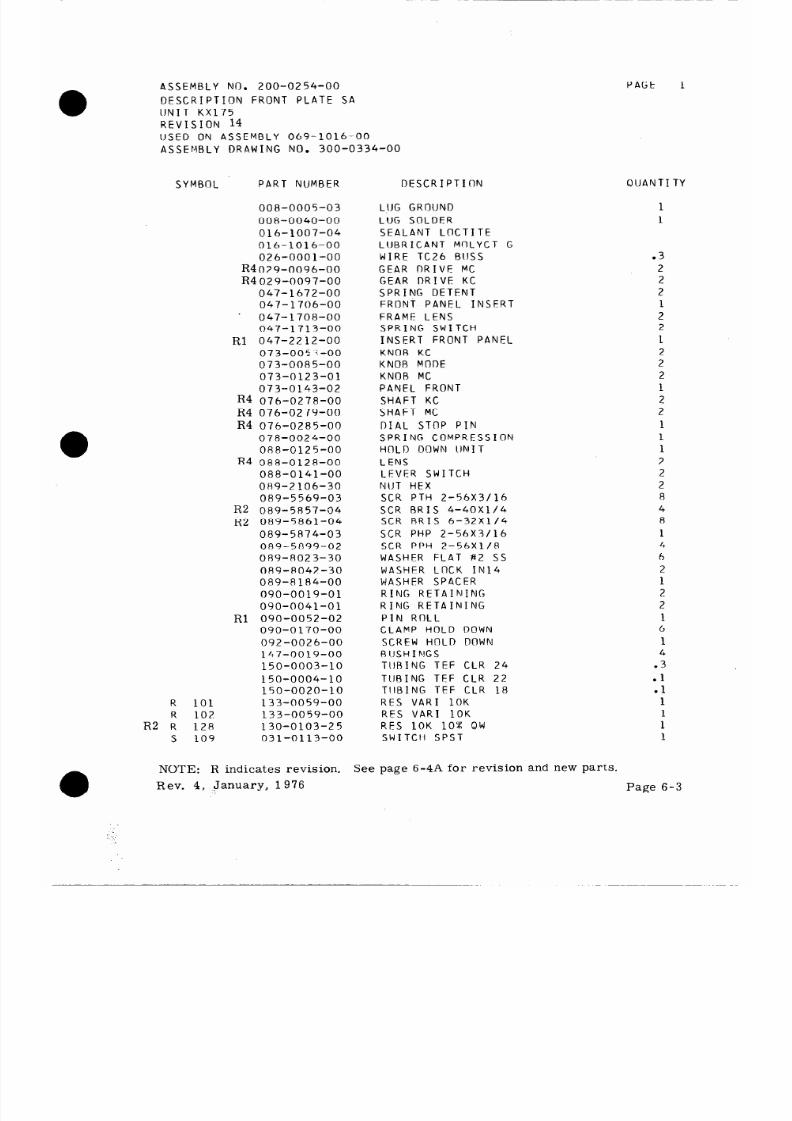
8/9/2019 KX 170A - Maintenance Manual Honeywell
http://slidepdf.com/reader/full/kx-170a-maintenance-manual-honeywell 236/586
ASSEMBLY NO. 200-0254-00
DESCRIPTION FRONT PLATE SA
IJNIT KX175
REVISION 14
LJSED ON ASSEMBLY 069-1016-00
ASSEMBLY DRAWING NO. 300-0334-00
SYMBOL PART NUMBER
DESCRIPTION
QlJANTI TY
008-0005-03
008-0040-00
016-1007-04
016-1016-00
026-0001-00
R4029-0096-00
R4 029-0097-00
047-1672-00
047-1706-00
' 047-1708-00
047-1713-00
Rl 047-22 12-00
073-005 i-00
073-0085-00
073-0123-01
073-0143-02
R4 076-0278-00
R4 076-0279-00
R4
076-0285-00
078-0024-00
088-0125-00
R4 088-0128-00
088-0141-00
089-Z 106-30
089-5569-03
R2
089-5857-04
R2 089-5861-04
089-5A74-03
089-5899-02
089-8023-30
089-8042-30
089-8184-00
090-0019-01
090-0041-01
Rl 090-0052-02
090-0170-00
092-0026-00
147-0019-00
150-0003-10
150-0004-10
150-0020-10
R
101 133-0059-00
R2 R"
102 133-0059-00
128 130-0103-2 5
S 109 031-0113-00
LlJG GROUND
LUG SDLDER
SEALANT LOCTITE
LIJBRICANT MDLYCT G
WIRE TC26 BIJSS
GEAR DRIVE MC
GEAR DRIVE KC
SPR I NG DETENT
FRDNT PANEL INSERT
FRAME LENS
SPRING SWITCH
INSERT FRONT PANEL
KNDR KC
KNOB ML-JOE
KNOB MC
PANFL FRONT
SHAFT KC
SHAFT MC
DIAL STDP PIN
SPRING CDMPRESSIDN
HOLD DOWN IJNIT
LENS
LEVER SWITCH
NIJT HEX
SCR PTH 2-56X3/16
SCR RRIS 4-40X1/4
SCR RRIS 6-32X1/4
SCR PHP 2-56X3/16
SCR PPH 2-56X1/8
WASHER FLAT #2 SS
WASHFR LOCK IN14
WASHER SPACER
RING RETAINING
RING RETAINING
PIN ROLL
CLAMP HOLD DOWN
SCREW HOLD DOWN
RUSHINGS
TIJRING TEF CLR 24
TUBING TEF CLR 22
TllBING TEF CLR 18
RES VARI 10K
RES VARI 10K
RES 10K 10X QW
SWITCH SPST
1
1
.3
2
2
2
1
2
2
1
2
2
2
1
2
2
1
1
2
2
2
8
4
8
1
4
6
2
1
2
2
1
6
1
4
.3
.l
.l
1
1
1
NOTE: R indicates revision.
Rev. 4, ,January, 1976
See page 6-4A for revision and new parts.
Page 6-3
PAGE
1
:.
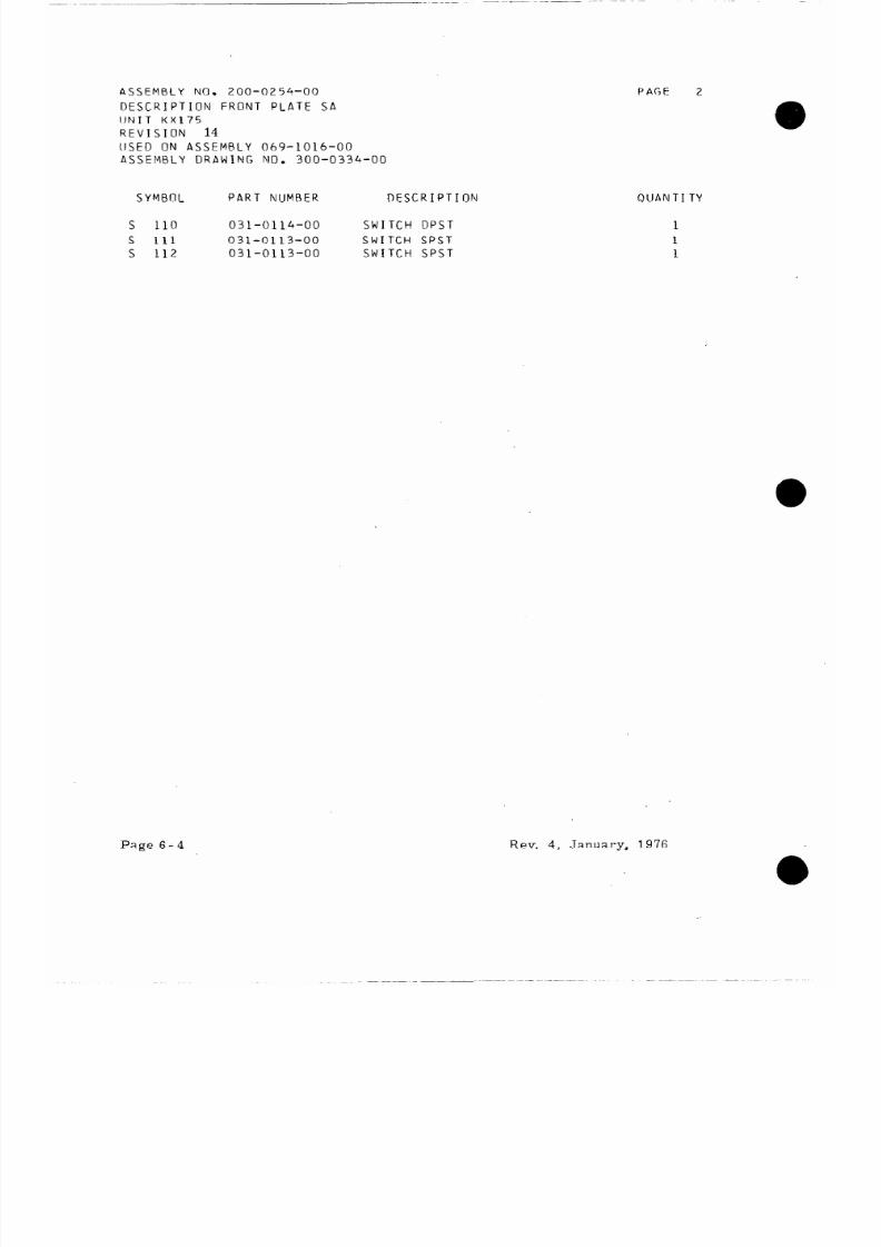
8/9/2019 KX 170A - Maintenance Manual Honeywell
http://slidepdf.com/reader/full/kx-170a-maintenance-manual-honeywell 237/586
ASSEMBLY NO. 200-0254-00
DESCRIPTION FRONT PLATE SA
IJNIT KX175
REVISION
14
USED ON ASSEMRLY O69-1016-00
ASSEMBLY DRAWING NO. 300-0334-00
SYMBOL
PART NUMBER
DESCRIPTION
S
110 031-0114-00
SWITCH DPST
S
111 031-0113-00
SW1TCH SPST
S 112
031-0113-00
SWITCH SPST
Page 6-4
PAGE 2
OUANTI TY
1
1
1
Rev. 4, January, 1976
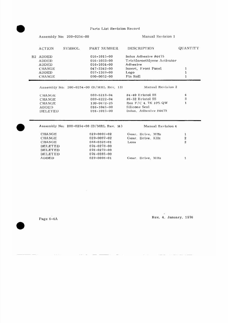
8/9/2019 KX 170A - Maintenance Manual Honeywell
http://slidepdf.com/reader/full/kx-170a-maintenance-manual-honeywell 238/586
Parts List Revision Record
Assembly No: 200-0254-00
Manual Revision 1
ACTION SYMBOL PART NUMBER DESCRIPTION QUANT TTY
R2 ADDED 016-1015-00
Indus Adhesive #44 75
ADDED
016-1033-00
Trichloroethlyene Activator
ADDED 016-1034-00
Adhesive
CHANGE 047-2342-00
Insert, Front Panel
1
ADDED 057-1369-00
Logo
1
CHANGE 090-0052-00
Pin Roll
1
Assembly No: 200-0254-00 (B/MRL Rev. 13)
Manual Revision 2
CHANGE 089-6218-04
#4-40 Bristol SS
CHANGE 089-6222-04 #6-32 Bristol SS
CHANGE 130-0472-25
Res F/C 4. 7K 10% QW
ADDED
016-1045-00
Silicone Seal
DELETED
016-1015-00
Indus. Adhesive #4475
4
8
1
Assembly No: 200-0254-00 (B/MRL Rev. 14)
Manual Revision 4
CHANGE 029-0096-02
Gear, Drive, MHz
1
CHANGE 029-0097-02
Gear, Drive. KHz
2
CHANGE 088-0326-01
Lens
2
DELETED 076-0278-00
DELETED 076-0279-00
DELETED 076-0285-00
ADDED 029-0096-01
Gear. Drive, MHz
1
Page 614A
.:
Rev. 4, January, 1976
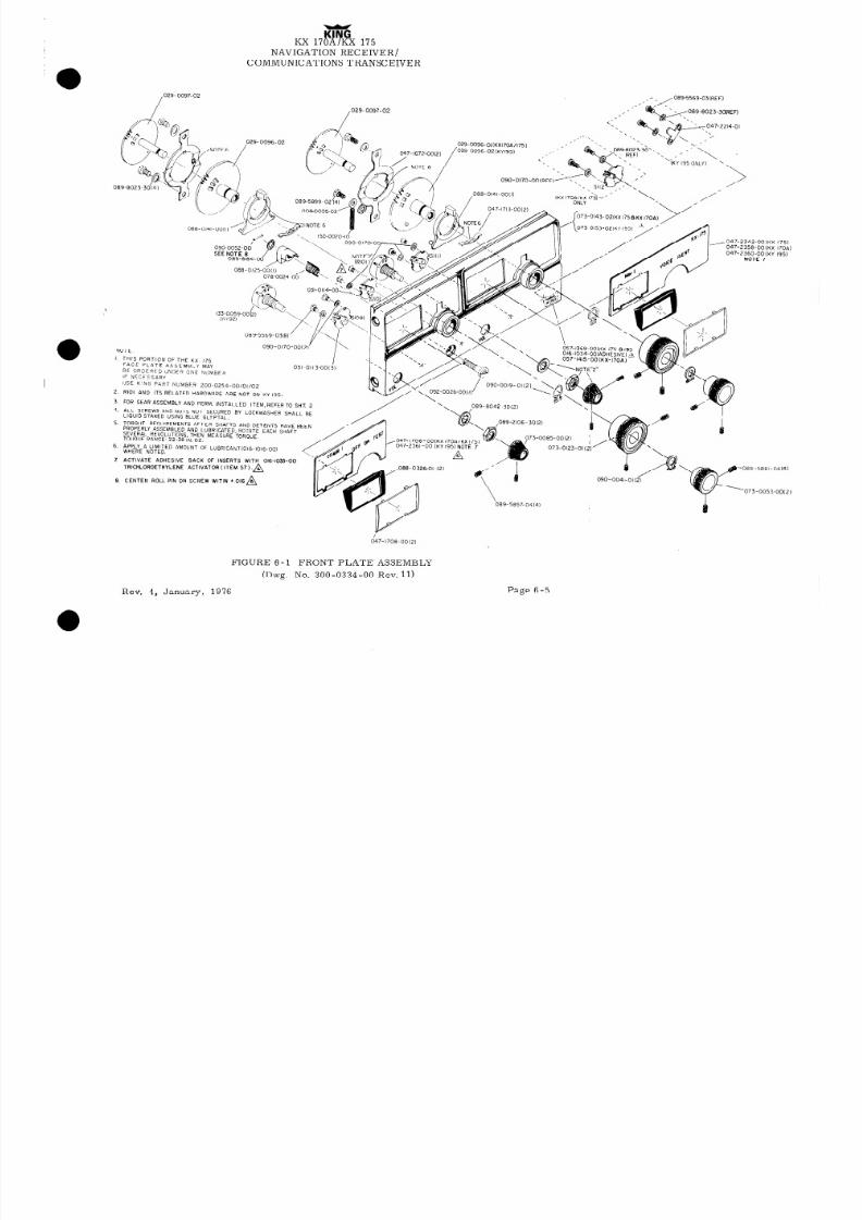
8/9/2019 KX 170A - Maintenance Manual Honeywell
http://slidepdf.com/reader/full/kx-170a-maintenance-manual-honeywell 239/586
KI G
KX 170A
r
KX
NAVIGATION RECEIVER/
COMMUNICATIONS TRANSCEIVER
,
- , ,0895569 -03(REF,)
088-0141.OO(l1’
.I,._?. r
-.-.“” ’ c 0
I&n nnn
/047-2342-OO(KX
047-235%OO(KX
047-2360.OO(KY
NOTE 7
088-0125-O&
078-0024~00
029-0096-02
029.0096.Ol(KXl70A/I75)
029.0096-02IKYl95)
090-0170-OOtREF)
089-8023-30
om-0141-OOII)
NV I t
1. THIS PORTION
OF
THE KX~
175
FACE PLATE ASSEMBLY MAY
BE ORDERFD UNDER ONE NUMBER
-.,” ““I.,,
IF NECFSSARY
/
\
i- 090-00l9-01~2;.’ ,&R jJSE K’NG PART NUMBER ZOO-0254.00/01/02
2. RIOI AND ITS RELATED HARDWARE ARE NOT ON KY 195.
3 FOR GEAR ASSEMBLY AND PERM. INSTALLED ITEM,REFER TO SHT. 2
4. ALL SCREWS AND NUTS NOT SECURED BY LOCKWASHER SHALL BE
LIQUID STAKED USING BLUE GLYPTAL.
5. TORQUE REQUIREMENTS AFTER SHAFTS AND DETENTS HAVE B
PROPERLY ASSEMBLED AND LUBRICATED ROTATE EACH SHAFT
SEVERAL REVOLUTIONS, THEN MEASURE TORQUE.
TOUOUE RANGE: 22-28 ,N:OZ.
6. APPLY A LIMITED AMOUNT OF LUBRICANT(016-1016-00)
WHERE NOTED.
’
089-2106-30(2)
73-0085-OO(2)
073-0123-01 I21
7 ACTIVATE ADHESIVE BACK OF INSERTS WITH 016-1033-00
TRICHLOROETHYLENE ACTIVATOR ( ITEM 57) .A
B. CENTER ROLL PIN ON SCREW WITIN ’ 016A
FIGURE 6-l FRONT PLATE A SSEMBLY
(Dwg. No. 300-0334-00 Rev. 11)
Rev. 4, January, 1976
Page 6-5
073-0053.OO(2)

8/9/2019 KX 170A - Maintenance Manual Honeywell
http://slidepdf.com/reader/full/kx-170a-maintenance-manual-honeywell 240/586
ASSEMBLY ND. 200-0253-00
DESCRIPTION SWITCH HEAD SA
UNIT KX175
PAGE 1
REVISION 8
lJSED ON ASSEMBLY 069-1016-00
ASSEMBLY DRAWING NO. 300-0333-00
SYMBOL
PART NUMBER DESCRIPTION
QIJANTI TY
008-0001-01
008-0005-03
016-1004-00
~2 016-1008-05
016-1016-00
025-0018-00
025-0018-30
025-0018-40
025-0018-90
R2 025-0018-99
026-0001-00
R2 029-0095-00
047-1675-01
047-1714-00
047-2115-00
047-2208-02
R2 076-0284-01
R2 076-0284-02
076-0298-00
076-0298-01
076-0298-03
076-0299-00
R2 076-0472-00
R2 076-0472-01
R2 076-0473-00
088-0136-00
R.2 088-0213-10
R2 088-0213-11
R2 088-0213-12
089-2005-37
089-2076-30
089-2140-00
089-5381-21
089-5857-04
R2089-5857-06
089-5903-04
389-5903-06
R2089-6289-03
089-8003-34
089-8023-30
089-8025-30
Rl 089-8079-10
090-0140-02
090-0160-00
091-0015-00
NOTE: R indicates revision.
Ke.v. 1 January, 1972
LUG GROlJND
LUG GROUND
THERMAL COMPOUND
ADHESIVE GLYPTAL
LUBRICANT MDLYCT G
WIRE CW26 BLACK
WIRE CW26 ORN/BLK
WIRE CW26 YEL/BLK
WIRE CW26 WHT/BLK
WIRE CW26 WHITE
WIRE TC26 BlJSS
GEAR FACE
SIJPPCIRT DIAL
BRACKET SW ITCH
BRACKET SW1 TCH
PLATE DIAL MTG
SHAFT DIAL GEAR
SHAFT DIAL GEAR
SPACER
SPACER
SPACER
COLLAR
SWITCH SHAFT
SWITCH SHAFT
SWITCH SHAFT
FILTER LAMP BLUE
CUtJNTER WHFFL W/MK
COIJNTER WHEEL W/MK
COUNTER WHEEL W/MK
NOT STOP 2-56
NUT 4-40
NUT ESNA #4
SC MACH ‘4-40X5/16
SCR BRIS 4-40X1/4
SCR BRIS 4-40X3/8
SCR PPH 4-40X1/4
SCREW 4-40X3/8
SCREW SHH 4-40X1/4
WASHER SPLITLOCK 4
WASHER FLAT #2 SS
WASHER #4
WASHER
SOCKET LAMP
SOCKET LAMP
GROMMET RIJBRFR
See page 6-9A for revision and new parts
2
7
1.1
.7
.6
.6
1.4
.8
2
1
1
1
1
1
1
4
10
2
2
1
1
2
2
2
1
1
4
2
6
4
4
4
2
2
6
2
4
2
2
1
1
3
Page 6-7

8/9/2019 KX 170A - Maintenance Manual Honeywell
http://slidepdf.com/reader/full/kx-170a-maintenance-manual-honeywell 241/586
ASSEMBLY NO. 200-0253-00
DESCRIPTION SWITCH HEAD SA
UNIT KX175
REVISION 8
USED ON P,SSEMBLY 069-1016-00
ASSEMBLY DRAWING NO.
300-0333-00
SYMBOL P4RT NIJMBER
C
C
C
C
C
CR
CR
CR
CR
R2 CR
R2 CR
R2 CR
R2 CR
R2
cr<
R2 CR
R2 CR
R2 CR
OS
DS
0
8
cl
0
0
R2 “K
R2 R
R2 R
R2 R
R2 R
R2 R
R2 R
R2 R
R.2 R
R2 R
R
R
R
R
101
102
103
104
105
101
102
103
104
105
106
107
108
109
110
111
112
101
102
101
102
103
104
105
103
111
112
113
114
115
116
117
118
119
120
125
126
127
129
DESCRIPTION
091-0015-11
GROMMET RtJRRER
091-0018-05
WASHER NYLON
091-0068-04
WASHER SHntJLDER
150-0003-10
TlJBING TEF CLR 24
R2 150-0005-10 TUBING TEF CLR 20
150-0020-10 TtJBING TEF CLR 18
113-5151-01
CAP 15OPF 10% X5F
097-0056-33
CAP 1OOlJF 16V
097-0056-33
CAP 1OOUF 1hV
113-5151-01 CAP 150PF 10% X5F
113-5151-01 CAP 15OPF 10% X5F
007-6021-00 DIODE TS-2
007-5026-00 DIODE ZENER 9.1V
007-5016-00 DIODE ZENER 5.1V
007-6021-00
DIODE TS-2
007-6033-00
DIODE lN270
007-6033-00 DIODE lN270
007-6033-00
DIODE lN270
007-6033-00 DIODE lN270
007-6033-00
DIODE lN270
007-6033-00
DIODE lN270
007-6033-00 DIODE lN270
007-6033-00
DIODE lN270
037-0007-10 LAMP BCJLB 14V
037-0007-10
LAMP BIJLB 14V
007-OlB4-01
TRANSISTOR TA7557
007-0184-01
TRANSISTOR TA7557
007-0078-02 TR’ANS I STDR 2N3416
007-0078-00
TRANSISTOR 2N3415
007-0078-02 TRANSISTOR 2N3416
130-0102-25
RES 1K 10% OW
136-2941-22
RES 2.94K 1% EW
136-4020-22 RES 402 1% EW
136-4530-22 RES 453 1% EW
136-5110-22
RES 511 1% EW
136-5620-22
RES 562 lx EW
136-6340-22
RES 634 1% EW
136-6980-22 RES 698 1% EW
136-7870-22 RES 787 14: EW
136-8660-22
RES 866 1% EW
136-6340-22
RES 634 1% EW
130-0680-33 RES 680HM 5% HW
130-0750-23 RES 75 5% QW
130-0750-23 RES 75 5X QW
130-0102-25 RES 1K 10% OW
NOTE: R indicates revision.
Page 6-8
OlJANTI TY
1
2
2
.5
.l
.6
1
1
1
1 1
1
1
1
i
1
1
1
1
1
1
1
0
See page 6-9A for revision and new parts
Rev. 2, December, 1972
PAGE 2

8/9/2019 KX 170A - Maintenance Manual Honeywell
http://slidepdf.com/reader/full/kx-170a-maintenance-manual-honeywell 242/586
ASSEMBLY NO. 200-0253-00
DESCRIPTION SWITCH HEAD SA
(INIT KX175
REVISIDN 8
(ISED ON ASSEMBLY 069-1016-00
ASSEMBLY DRAWING NC). 300-0333-00
R
R
R
R
S
R2 S
S
R2 s”
R2 S
R2:
SYMBOL
PART NIJMBER
DESCRIPTION
130
130-0152-23 RES 1.5K 5% QW
131
130-0471-23 RES 470 5% QW
132
133-0016-02
RES VARI 1K
133 130-0102-25
RES 1K 10% OW
101
031-0104-00 WAFER SWITCH
102
031-0107-00
WAFER SWITCH
103
031-0106-00 WAFER SWITCH
104
031-0105-00
WAFER SWITCH
105
031-0154-00 SWITCH WAFER
106
031-0155-00
SWITCH WAFER
107
031-0156-00 SWITCH WAFER
108
031-0157-00 SWITCH WAFER
PAGE 3
OIJANTI TY
1
1
1
1
1
1
1
1
1
1
1
1
NOTE: R indicates revision.
See page 6- 10 for r: -ision aild new parts.
Rev. 2, December, 1972
I
Page 6-9
8/9/2019 KX 170A - Maintenance Manual Honeywell
http://slidepdf.com/reader/full/kx-170a-maintenance-manual-honeywell 243/586
0
Parts List Revision Record
Assembly No: 200-0253-00
Manual Revision 1
c
ACTION
SYMBOL PART NUMBER
DESCRIPTION
QUANTITY
R2 ADDED
CR113 007-6033-00
Diode, lN270 1
DELETE 089-8079-10 Washer 2
Assembly No: 200-0253-00 (B/MRL Rev. 8)
Manual Revision 2
CHANGE
DE LE’I‘E
DELETE
DELETE
DELETE
DELETE
DELETE
DELETE
DELETE
DELETE
DELETE
DELETE
DELETE
DELETE
DELETE
DELETE
DELETE
DELETE
DELETE
DELETE
DELETE
CHANGE
CHANGE
CHANGE
CHANGE
CHANGE
DELETE
DELETE
DELETE
DELETE
DELETE
DELET/E
..-
R112
R113
R114
R115
R116
R120
R117
R118
R119
s102
s105
S106
S108
Rlll
CR105
CR106
CR107
CR 108
CR109
CR110
025-0018-99
029-0095-00
076-0284-01
076-0284-02
136-4020 -22
136-4530 -22
136-5110-22
136-5620-22
136-6340-22
136-6340 -22
136-6980 -22
136 -7870 -22
136-8660-22
088-0213-10
016-1008-05
076-0472-00
076-0472-01
076-0473-00
089-5857-06
089-6289-03
200 -0 57 5 -04
200-0575-01
200-0575-02
200-0575-03
136-294 l-22
007-6033-00
007-6033-00
007-6033-00
007-6033-00
007-6033-00
007-6033 -00
Tubing, Teflon #20
Wire #26 Wht.
Gear Face
Shaft Dial Gear
Shaft Dial Gear
Res. 402 1% EW
Res. 453 1% EW
Res. 511 1% EW’
Res. 562 1% EW
Res. 634 1% EW
Res. 634 1% EW
Res. 698 1% EW
Res. 787 1% EW
Res. 866 1% EW
Counter Wheel w/mk
Adhesive Glyptal
Switch Shaft
Switch Shaft
Switch Shaft
SCR BRIS 4 -40X3 /8
SCR SHH 4-40X1/4
Swtich Ass’y COMM
Switch Ass’y NAV
Switch Ass’y NAV
Switch Ass’y NAV
Res. 2. 94K 1% QW
Dio lN270
Dio lN270
Dio lN270
Dio lN270
Dio lN270
Dio lN270
.2
1. 4
2
1
1 .
1
1
1
1
1 .
1
1
1
1
2
1
1
1
4
6
1
1
1
1
1
1
1
1
1
1
1
Rev, 2, December, 1972
a
age ,6-10

8/9/2019 KX 170A - Maintenance Manual Honeywell
http://slidepdf.com/reader/full/kx-170a-maintenance-manual-honeywell 244/586
Assembly No: 200 -02 53 -00
Manual Revision 1
ACTION
SYMBOL
PART NUMBER DESCRIPTION
QUANTITY
DELETE
DELETE
DELETE
CHANGE
CHANGE
CR111
CR112
CR113
From
To
From
To
007-6033-00
007-6033-00
007-6033-00
088-0213-11
200-0576-02
088-0213-12
200 -0 578 -00
200 -0 578 -02
200-0576-04s’
200-0578-01
200-0576-03
Dio lN270
Dio lN270
Dio lN270
Counter Wheel w/mk
Wheel Ass’y NAV MHz
Counter Wheel w/mk
ADD
ADD
ADD
ADD
Wheel Ass’y COMM MHz
1
Gear Ass’y-COMM
1
Gear Ass’y NAV 1
Wheel Ass’y COMM KHz
1
Wheel Ass’y NAV KHz 1
Parts List Revision Record
Rev. 4 Jan. 1976
Page 6-11

8/9/2019 KX 170A - Maintenance Manual Honeywell
http://slidepdf.com/reader/full/kx-170a-maintenance-manual-honeywell 245/586
KI G
7
X 170A KX 175
NAVIGATION RECEIVER/
COMMUNICATIONS TRANSCEIVER
076-0298-05 -..,
,
-”
,/
/
‘\
/
_,__ 076-Of2zy -0 1
m...,. ^^A
-.-,,\
\
FIGURE 6-2
SWITCH HEAD SUB-ASSEMBLY
(Dwg. No.
300-0333-00 R-6)
Rev. 4 , January, 1976
Page 6-13

8/9/2019 KX 170A - Maintenance Manual Honeywell
http://slidepdf.com/reader/full/kx-170a-maintenance-manual-honeywell 246/586
KING
KX 170A/KX 175
NAVIGATION RECEIVER/
COMMUNICATIONS TRANSCEIVER
NOTES:
-
I. 0 NEARSIDE TERM.
2. ; FARSIDE TERM.
3. ‘.I
SWITCHES READ FROM LEFT SIDE OF UNIT
rPll8
/- PI08
PI09
-PI10
~031-0107-00
5102
200-0575-04
L031-0106-00
SlO3lO3
PI26
Pl25--,
PI36
7
r PI37
PI46
7
PI62
/
\CRIll
.Pl56
PI34 PI61
tSlSD6~ RzE& I ;ACK
200-0575-01 200-0573-02
SWITCHING HEAD SUB ASS’Y WIRING CHART
I
COLOR 1
REMARKS
U 1SLEEVED WITH (150-0003-10) .4 LG.
PART NO.
026-0001-00
”
*
II
025-O&8-00
II
”
FROM
Pll2EIPIl3(sIo3I
Pl29R Pl3O(slo5:
PI35 (SlO6)
Plo5(sIoI)
Pl47tSlO6)
Plo5(sIoI)
PI 19(SlO4)
Pl29(SlO5)
Pl55(SlO7)
DSIOI
DSIOI
DS102
Pl34tslO5)
Pl49tSlO6)
TO
‘II9 8 Pll8(SlO4)
PI51 (SlO7)
PI62 (S IO81
PlO6(SIOI)
Pl48tS 106)
Pl8OtGND)
LENGTH
A.2
I .2
14
42
64::
3:
8:0
655
* *
”
1.3 n
* m
II
.7 ”
BG
WHY/ELK
WHITE
BLACK
WHITE
YEL/BLK
ORNALK
SEE SHEET I FOR CONNECTIO NS
D 0,
II
”
II
II II
II
0, I
Y
”
”
025-0018-90
REF:
I
025-0618-40
025-0018-30
FIGURE 2-A SWITCH HEAD ASSEMBLY
(DWG. NO. 300-0333-00 SHT. 2 R-6)
Rev. 4, January, 1976
Page 6-15
8/9/2019 KX 170A - Maintenance Manual Honeywell
http://slidepdf.com/reader/full/kx-170a-maintenance-manual-honeywell 247/586
ASSEMBLY NO. 200-0248-00
DESCRIPTION NAV SMO BOARD SA
UNIT KX175
REVISION 11
USED ON ASSEMBLY 200-0252-00
ASSEMBLY
SYMBOL
c 201
C 202
c 203
C 204
c 205
C 206
c 208
C 209
c 210
C 211
c 212
R2 C 213
C 214
c 215
Rl C 216
C 217
c 218
C 219
c 220
c 221
c 222
C 223
C 224
C 225
c 226
C 227
c 228
c 229
C 230
C 232
C 233
c 234
C 235
c 236
C 237
DRAWING ND.
300-0325-C-10
PART NUMBER
DESCRIPTION
009-5136-01 NAV SMO BOARD
012-1038-00
DISC ADHESIVE
025-0018-22 WIRF CW26 RED
025-0018-99
WIRE CW26 WHITE
026-0001-00 WIRF TC26 BJJSS
026-0013-00
WIRE COAX RG178U
047-2 154-00 CAN CHOKE
088-0066-00
PLASTIC SPACER
150-0003-10
TUBING TEF CLR 24
150-0015-10 TIJBING TEF CLR 12
114-5152-00 CAP 1500PF X5F
096-1030-22
CAP TANT 221JF 20%
114-5152-00 CAP 1500PF X5F
118-0003-00
CAP 56PF 5% N750
118-0003-00 CAP 56PF 5% N750
113-5331-00
CAP 330PF
10X X5F
113-5681-00
CAP 6BOPF
10% X5F
114-7104-00
CAP
.lIlF 20x X5R
096-1030-17
CAP TANT 6.YlJF 203
105-0033-39 CAP MY
.0391JF 5%
105-0033-09 CAP MY
.0022UF 5%
096-1030-14
CAP TANT .68MF 5X
096-1030-22
CAP TANT 22lJF 20X
096-1030-22 CAP TANT 221JF 20%
113-3100-00 CAP 1OPF 5X N150
113-5681-00 CAP 6BOPF 10X X5F
113-5681-00
CAP 680PF
10X X5F
113-5471-00
CAP 470PF
10x X5F
113-3100-00 CAP 1OPF 5X N150
113-5681-00 CAP 6ROPF 1Om X5F
113-5681-00 CAP 680PF
1Or; X5F
113-5471-00
CAP 470PF
10x X5F
113-5101-01 CAP 1OOPF 10x X5F
113-3330-00
CAP 33PF 5% N150
114-5152-00
CAP 1500PF X5F
114-5152-00 CAP 1500PF X5F
114-5152-00
CAP 1500PF X5F
114-5152-00
CAP 1500PF X5F
113-3082-00 CAP 8.2PF 5% N150
113-3270-00
CAP 27PF 5X N150
113-3100-00 CAP 1OPF 5X Nl50
114-5152-00 CAP 1500PF X5F
113-3470-00 CAP 47PF 5X X5F
113-3820-00 CAP R2PF 5% X5F
114-5152-00
CAP 1500PF X5F
PAGE 1
QUANTITY
1
1
.5
.6
.8
1.2
1
1
.4
.l
1
1
1
1
1
1
NOTE: R indicates revision. See page 6-21A for revision and new parts.
Rev. 4, January, 1976
Page 6-17
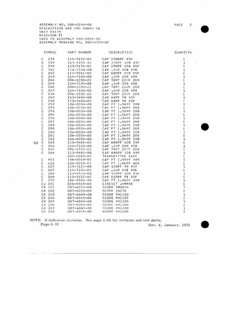
8/9/2019 KX 170A - Maintenance Manual Honeywell
http://slidepdf.com/reader/full/kx-170a-maintenance-manual-honeywell 248/586
ASSEMBLY NO. 200-0248-00
DESCRIPTION NAV SMCI ROARD SA
IJNIT KX175
REVIS ION 11
USED ON ASSEMBLY 200-0252-00
ASSEMBLY
DRAWING Nfl.
300-0325-00
SYMBOL PART NJJMBER DESCRIPTIOX
(
3UANTI TY
C 238
c 239
c 240
c 241
C 242
C 243
C 244
C 245
C 246
c 247
C 248
C 249
c 250
c 252
C 253
C 254
C 255
c 256
c 257
C 258
C 259
C 260
C 261
C 262
‘Rl c 263
c 2h4
c 265
C 266
114-5152-00
CAP 1500PF X5F
113-5151-01
CAP 15DPF
10x
X5F
113-5151-01
CAP 150PF 1OW X5F
114-7104-00
CAP .l JF 20% X5R
113-5681-00 CAP 680PF 10X X5F
114-7104-00
CAP
.11JF 20% X5R
096-1030-22 CAP TANT 22 JF 20%
114-7104-00
CAP .lIIF 20% X5R
096-1030-22
CAP TANT 22JlF 20%
114-7104-00
CAP .
11JF 20% X5R
096-1030-22
CAP TANT 22lJF 20%
113-3680-00
CAP 6BPF 5% X5F
113-3680-00
CAP 68PF 5% X5F
106-0034-00
CAP FT 1.5KPF 20%
106-0034-00
CAP FT 1.5KPF 20%
106-0034-00 CAP FT 1.5KPF 20%
106-0034-00
CAP FT
1
.SKPF 20%
106-0034-00
CAP FT 1.5KPF 20%
106-0034-00
CAP FT 1.5KPF 20%
106-0034-00
CAP FT 1.5KPF 20%
106-0034-00
CAP FT 1.5KPF 20%
106-0034-00
CAP FT 1.5KPF 20%
106-0034-00
CAP FT
1.5KPF 20X
106-0034-00
CAP FT 1.5KPF 20X
113-5681-00 CAP 68OPF 104: X5F
114-7104-00
CAP .11JF 20% X5R
096-1030-22 CAP TANT 22llF 201
113-5681-00
CAP 6AOPF 10X X5F
200-0083-00 TRANSMITTER ASSY
106-0018-01
CAP FT 1.5KPF 40%
106-0018-01
CAP FT 1.5KPF 40%
113-3121-00
CAP 120PF 5% X5F
114-7104-00
CAP .
1lJF 20X X5R
113-5471-00 CAP 470PF 10X X5F
113-3121-00 CAP 120PF 5% X5F
106-0034-00 CAP FT 1.5KPF 20%
026-0018-00
C IRCIJI T JLJMPER
007-4012-00 DIODE SMVh26
007-6033-00 DIflDF lN270
007-6045-00
DIODE FHllOO
007-6045-00
DIODE
FHllOO
007-6045-00 DIODE FHllOO
007-6045-00
DIODE FHllOO
007-6045-00
DIODE
FHllOO
007-6045-00 DIODE FHllOO
1
1
1
c 611
c 612
C 623
C 267
c 268
C 269
c 270
CJ 201
CR 201
CR 202
CR 203
CR 204
CR 205
CR 206
CR 207
CR 208
1
PAGE 2
a
NOTE: R indicates revision.
See page 6-22 for revision and new parts.
Page 6-18
Rev. 4; January, 1976

8/9/2019 KX 170A - Maintenance Manual Honeywell
http://slidepdf.com/reader/full/kx-170a-maintenance-manual-honeywell 249/586
ASSEMBLY ND. 200-024A-00
DESCRIPTION NAV SMO BOARD SA
UNIT KX175
REVIS ION 11
USED ON ASSEMBLY 200-0252-00
ASSEMBLY DRAWING NO. 300-0325-00
SYMBOL
CR 209
CR 210
CR 211
CR 212
CR 213
CR 214
I 201
I 202
I 203
I 204
I 205
I 206
I 207
I 208
L 201
L
202
L
203
L
204
L
205
R2 0 201
Q 202
0 203
R2 0 204
0 205
R2 0 206
R2 0 207
R2 0 208
Q 209
Q 210
cl 211
R
201
R
202
R4 :: ‘z;:
R 205
R 206
R
207
R 208
R
209
R 210
R 211
R2
R
212
R 213
R 214
R 215
PART NIIMBER DESCRIPTION
007-6045-00
DIODE FHllOO
007-6045-00
DIODE
FHllOO
007-6035-00 DIODE lN816
007-6035-00
DIODE lNA16
007-6033-00 DIODE lN270
007-5016-00
DIODE ZENFR 5.1V
120-0019-00 INT CKT U6B902059X
120-0021-00
INT CKT LJ68930059X
120-0014-00
INT CKT U6A900259X
120-0016-00
INT CKT UbA900459X
120-1035-00
INT CKT U6A998979X
120-0021-00 INT CKT lJ68930059X
120-1029-00
INT CKT MC817P
120-1029-00
INT CKT MC817P
019-2151-00
COIL, vco
019-2082-70 CHOKE 240iJH 5%
019-2054-16
CHOKE
l.OUH 5%
019-2054-16 CHOKE l.OUH 5%
019-2054-13 CHOKE . 56UH 5X
007-0119-00 TRANS
I
STUR 2N4917
007-0195-00
TRANS.1 STOR MPSHlO
007-0195-00
TRANSISTOR MPSHlO
007-0119-00 TRANSISTOR 2N4917
007-0078-00
TRANSISTOR 2N3415
007-0119-00
TRANSISTOR 2N4917
007-0119-00 TRANSISTOR 2N4917
007-0119-00
TRANSISTOR 2N4917
007-0195-00
TRANSISTOR
MPSHlO
007-0078-00
TRANSISTOR 2N3415
007-0078-00
TRANSISTOR 2N3415
130-0101-25 RES
100 10X
QW
130-0103-23
RES 1OK 5% QW
130-0471-23
RES 470 5% QW
130-0472-23
RES 4.7K 5X QW
130-0510-23
RES 51 5X QW
130-0473-25
RES 47K
10%
QW
130-0510-23
RES 51 5X QW
130-0271-23 RES 270 5% QW
130-082 l-23
RES 820 5% QW
130-0112-23 RES
l.lK 5%
QW
130-0391-23
RES 3900HM 5X QW
130-0332-23 RES 3.3K 5% QW
130-0471-2 5 RES 470 10X QW
130-0102-25 RES 1K 10% QW
130-0152-25 RES 1.5K 10% QW
NOTE: R indicates revision.
See page 6-22 for revision and new parts
Rev. 4, January, 1976
PAGE 3
QUANTI TY
1
1
1
1
1
1
1
1
1
1
1
1
1
1
1
1
1
1
1
1
1
1
1
1
1
1
1
1
1
1
1
1
1
1
1
Page 6-19

8/9/2019 KX 170A - Maintenance Manual Honeywell
http://slidepdf.com/reader/full/kx-170a-maintenance-manual-honeywell 250/586
ASSEMBLY NO. 200-0248-00
DESCKIPTIDN NAV SMO BOARD SA
IJNIT KX175
REVISION 11
IISED ON ASSEMBLY 200-0252-00
ASSEMBLY
DRAWING ND,
300-032 5-00
SYMB0.L
PART NUMBER
R 216
130-0101-25
R 217
130-0392-23
Rl R 218
130-0472-23
R 219
130-0271-23
R 220 130-0101-25
R 221 130-0392-23
Rl R 222
130-0472-23
R 223
130-0271-23
R 224
130-0272-23
R 225 130-0221-23
R 226
130-0512-23
R 227
130-0101-23
R 228
130-0151-23
R 229
130-0470-25
R 230
130-0100-23
R 231
130-0470-23
R 232
130-0301-23
R 233
130-0101-25
R 234
130-0222-23
R 235
130-0911-23
R 236
130-0152-23
R 237
130-0302-23
R 238
130-0331-23
R 239 130-0201-23
R 240
130-0241-2 3
R 241
130-0820-23
R 242
130-0471-23
R 243
130-0471-23
R 244
130-0472-23
R 245
130-0472-23
R 247 130-0472-23
R 248
130-0472-23
R 249
130-0222-23
R 250
130-0222-25
R 251
130-0222-2 5
R 252
130-0222-25
R 253
130-0222-2 5
R 254
130-0222-25
R 255 130-0222-25
R 256 130-0222-25
R 257 130-0222-25
R 259
130-0102-25
R 259
132-0107-30
R 260
130-OlRl-23
T 201
019-2109-00
DESCRIPTIflN
RES 100 10% OW
RES 3.9K 5% (314
RES 4.7K 5% QW
RES 270 5% QW
RES 100
10%
QW
RES 3.9K 5% Q d
RES 4.7K 5% QW
RES 270 5% QW
RES 2.7K 5% Q\d
RES 220 5% Qw
RES 5.2K 5% QW
RES
100 5%
QW
RES 150 5% QW
RES 47 10% QW
RES
10 5% OW
RES 470HM 5% OW
RES 300 5% OhI
RES
100 10%
QW
RES 2.2K 5% QW
RES 910 5% QW
RES 1.5K 5% QW
SES 3K. 5% QW
RES 330 5% Qlrl
RES 200 5% QW
RES 240 5% QW
RES 82 5% QW
RES 470 5% QW
RES 470 5% OW
RES 4.7K 5% QW
RES 4.7K 5% QW
RES 4.7K 5% QW
RES 4.7K: 5% QW
RES 2.2K 5X QW
RES 2.2K 10% QW
RES 2.2K
10X O’rl
RFS 2.2K
10X
QW
RES 2.2K 10% QW
RES‘ 2.2K 10% QW
RES 2.2K
10% (3W
RES 2.2K
10%
QW
RES 2.2K 10% QW
RES 1K
10%
OW
RES WW 12 5”h’ 3
l/4
RES
180 5%
DW
I NDIJCTOR VAR
I
PAGE 4
(3lJANTI TY
1
1
1
1
1
1
1
1
1
1
1
1
1
1
1
1
1
1
1
1
I.
1
1
1
NOTE: R indicates revision.
See page 6-22 for revision and new parts.
Page 6-20
Rev. 4, January. 1976
l

8/9/2019 KX 170A - Maintenance Manual Honeywell
http://slidepdf.com/reader/full/kx-170a-maintenance-manual-honeywell 251/586
ASSEMBLY NO. 200-0248-00
PAGE 5
DESCRIPTION NAV SMO BOARD SA
IJNIT KX175
REVISION 11
IJSED ON ASSEMBLY 200-0252-00
ASSEMBLY DRAWING NO. 300-0325-00
SYMBOL PART NkJiurRER
DESCRIPTION
T 202
T 203
T 204
T 205
T 206
T 207
Y 201
Y 202
019-3044-00 TRANSFORMER RF
019-3044-00 TRANSFORMER RF
019-5056-02 TRANSFORMER MIXFR
019-5056-02 TRANSFORMER MIXER
019-5056-02 TRANSFflRMER MIXER
019-5056-02 TRANSFflRMER MIXER
044-0027-00 XTAL 53.93125MHZ
044-002 R-00 XTAL 4OOKHZ
OlJANTI TY
Rev. 4, January, 1976
Page 6-21

8/9/2019 KX 170A - Maintenance Manual Honeywell
http://slidepdf.com/reader/full/kx-170a-maintenance-manual-honeywell 252/586
Parts List Revision Record
Assembly No: 200-0248-00
Manual Revision 1
ACTION SYMBOL PART NUMBER
DESCRIPTION QUANT IT Y
CHANGE
C216
113-3150-00
Cap. 15pf, 570, N150 1
ADDED
C231
113-3100-00
Cap. lOpf, 570, N150
1
DELETE
C263
113-5681-00
Cap. 680pf, lo%, X5F 1
R4 ADDED
L206
019-2084-00
Choke 6. 8pf, 5% 1
ADDED
L207
019-2084-06
Choke . 27pf, 5% 1
CHANGE
R218
130-0242-23
Res. 2. 4K, 50/o, QW
1
CHANGE
R222
130-0392-23
Res. 3. 9K, 5%, QW
1
Assembly No: 200-0248-00 (B/MRL Rev, 10)
Manual Revision 2
DELETE
CHANGE
CHANGE
ADD
CHANGE
CHANGE
CHANGE
CHANGE
R212
130-0332-23
C213 114-7104-00
R207
130-0202-23
090-0104-04
Q201
007-0238-00
Q204
007-0238-00
Q206
007-0238-00
9207
007-0238-00
Res. F. C. 3. 3K 5% QW
1
Cap D/C . lpf *200/ 12V 1
Res. F. C.
2. OK 5% QW
1
Solder Ring, preform
12
Tstr. FPN 4917
1
Tstr. FPN 4917
1
Tstr. FPN 4917
1
Tstr. FPN 4917
1
CHANGE
Q208
007-0238-00
Tstr. FPN 4917
1
l
Assembly No: 200-0248-00 (B/MRL Rev. 11)
Manual Revision 4
CHANGE R204 130-0362-23
Res. F/C 3. 6K 5% QW 1
CHANGE L206 019-2084-40
Choke, 6.
8pf 5%
1
Page 6-22
Rev. 4, January, 1976

8/9/2019 KX 170A - Maintenance Manual Honeywell
http://slidepdf.com/reader/full/kx-170a-maintenance-manual-honeywell 253/586
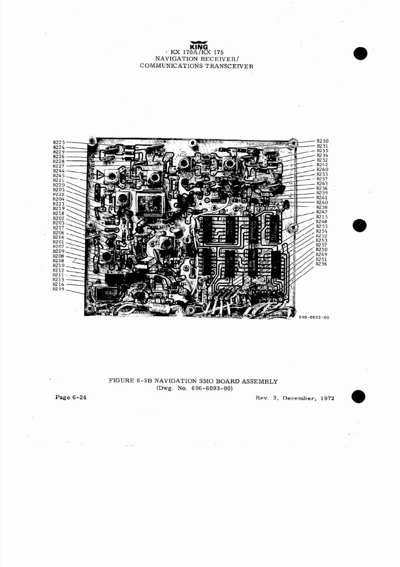
8/9/2019 KX 170A - Maintenance Manual Honeywell
http://slidepdf.com/reader/full/kx-170a-maintenance-manual-honeywell 254/586
R225
R224
R.229
R226
R228
R227
R244
R245
R221
R220
R205
P222
R204
R223
R219
R218
R202
R203
R2r7
tiO6
R216
R201
R207
R209
R208R258
RzlO
R212
R211
R213
R214
R259
KI G
7
. KX 170A
KX 175
NAVIGATION RECEIVER/
COMMUNICATIONS TRANSCEIVER
.R230
.R231
:g;
'R232
'R242
.R260
R233
a.237
R-243
R236
R239
R241
R240
R238
'R247
R215
R248
R255
R254
R252
R253
R257
R-250
R249
R251
R256
193 00
Page 6-24
FIGURE 6-3B NAVIGATION SMO BOARD ASSEMBLY
(Dwg. No. 696-6093-00)
Rev. 2, December, 1972
l

8/9/2019 KX 170A - Maintenance Manual Honeywell
http://slidepdf.com/reader/full/kx-170a-maintenance-manual-honeywell 255/586
KING
KX 170A/KX 175
NAVIGATION RECEIVER/
COMMUNICATIONS TRANSCEIVER
4206
L203
T206
CR204
T205
CR203
CJ201
T204
CR206
CR.205
Y202
T203
L201
L206
CR201
%a022
L207
FIGURE 6-3C NAVIGATION SMO BOARD ASSEMBLY
Rev. 1 January, 1972
Page 6-25

8/9/2019 KX 170A - Maintenance Manual Honeywell
http://slidepdf.com/reader/full/kx-170a-maintenance-manual-honeywell 256/586
ASSEMBLY NO. 200-0252-00
DESCRIPTION NAV SMO SA
UNIT KX175
REVISION
USED ON ASSEMBLY 069-1016-00
ASSEMBLY DRAWING NO. 300-0332-00
SYMBOL PART NIJMBER
DESCRIPTION
016-1011-00
PLIOBOND CEMENT
047-2230-02
TRAY NAV SMO
076-0165-09
SPACER
076-0339-00
SPACER
076-0343-00
SPACER
089-5874-03
SCR PHP 2-56X3/16
089-5878-05
SC PPH 4-40X5/16
091-0088-01
NAV INSIJLATION
200-0248-00
NAV SMfl BOARD SP
Page 6-26
0
PAGE
1
OUANTI TY
a
ev. 1 January, 1972

8/9/2019 KX 170A - Maintenance Manual Honeywell
http://slidepdf.com/reader/full/kx-170a-maintenance-manual-honeywell 257/586
Parts List Revision Record
Assembly No. 200-0252-00 Manual Revision 1
ACTION SYMBOL
PART NUMBER
DESCRIPTION QUANTITY
No Change
Rev. 1 January, 1972
Page 6-27

8/9/2019 KX 170A - Maintenance Manual Honeywell
http://slidepdf.com/reader/full/kx-170a-maintenance-manual-honeywell 258/586
076
KX l$ ) & 175
NAVIGATION RECEIVER/
COMMUNICATIONS TRANSCEIVER
076-0343-OO.,
076-0165-09
089-5878-05
200-0248-00
47-22 30-
091-0088-01
46
\
089-5874-03 300-0332-00
FIGURE 6 -4 NAVIGATION SMO SUB-ASSEMBLY
.02
(R-0)
Page 6-28
Rev. 1 January, 1972
a

8/9/2019 KX 170A - Maintenance Manual Honeywell
http://slidepdf.com/reader/full/kx-170a-maintenance-manual-honeywell 259/586
ASSEMBLY ND. 200-0247-00
DESCRIPTION COMM SMO SA
UNIT KX175
REVISION 9
USED ON ASSEMBLY 200-0251-00
ASSEMBLY DRAWING NO. 300-0324-00
SYMBOL
c 301
C 302
c 303
C 304
c 305
C 306
c 307
C 308
c 309
c 310
C 311
C 312
C 314
C 315
C 316
C 317
C 318
C 319
C 320
C 321
C 322
C 323
C 324
C 325
C 327
C 328
C 329
c 330
C 331
C 333
C 335
C
336
PART NUMBER DESCRIPTION
009-5137-02
COMM SMO BOARD .
012-1038-00 DISC ADHESIVE
025-0018-91
WIRE CW26 WHT/BRN
025-0018-98
WIRE CW26 WHT/GRY
025-0018-99 WIRE CW26 WHITE
026-0001-00 WIRE TC26 BtISS
026-0013-00
WIRE COAX RG17811
047-1852-01 ENCLI-ISURE OSC
047-1853-01
ENCLI-ISURE VCO
088-0066-00 PLASTIC SPACER
150-0003-10 TUBING TEF CLR 24
150-0005-10 TUBING TEF CLR 20
150-0015-10 TUBING TEF CLR 12
106-0034-00 CAP FT l.SKPF 20%
106-0034-00 CAP FT 1.5KPF 20%
106-0034-00 CAP FT 1.5KPF 20%
113-5471-00
CAP 470PF 10% X5F
113-3100-00 CAP 1OPF 5% N150
106-0034-00 CAP FT 1.5KPF 20%
106-0034-00 CAP FT ,l.SKPF 20%
113-5471-00 CAP 47dPF 10% X5F
113-5471-00 CAP 470PF 10% X5F
113-5471-00 CAP 470PF 10% X5F
113-5471-00 CAP 470PF 104: X5F
113-5471-00 CAP 470PF 10% X5F
102-0024-09 CAP VARI 7-35PF
102-0029-00 CAP VARI 2-27PF
096-1030-22 CAP TANT 221JF 20%
113-3270-00 CAP 27PF 5% N150
113-5471-00 CAP 470PF 10% X5F
106-0034-00 CAP FT 1.5KPF 209
113-5471-00 CAP 470PF 10% X5F
113-5471-00 CAP 470PF 10% X5F
114-7104-00 CAP .lUF 20% X5R
113-5471-00 CAP 470PF 109: X5F
113-5102-00 CAP 1KPF 10% X5F
113-3100-00
CAP 1OPF 5% N150
113-5331-00
CAP 330PF 10% X5F
114-7104-00
CAP .llJF 20X X5R
113-5471-00
CAP 470PF 10% X5F
113-3015-00
CAP 1.5PF 5% N150
106-0034-00
CAP FT l.SKPF 20%
113-5471-00
CAP 470PF 104: X5F
113-3120-00
CAP 12PF 5% N150
113-5471-00 CAP 470PF 10% X5F
PAGE 1
BUANTI TY
1
1
1.5
1.5
2.0
2.0
2.2
1
1
2
2 :4
.l
.2
1
1
1
1
1
1
1
1
1
1
1
1
1
1
1
1
1
1
1
1
1
1
1
1
1
1
1
1
1
1
1
1
NOTE: R indicates revision. See page 6-35 for revision and new parts,
Rev. 2, December, 1972
Page 6-29

8/9/2019 KX 170A - Maintenance Manual Honeywell
http://slidepdf.com/reader/full/kx-170a-maintenance-manual-honeywell 260/586
ASSEMBLY NO. 200-0247-00
DESCRIPTION COMM SMO SA
UNIT KX175
REVISION 9.
USED ON ASSEMBLY 200-0251-00
ASSEMBLY DRAWING NO. 300-0324-00
SYMBOL PART NUMBER
c 337
113-5471-00
C 338 113-3270-00
c 339 113-5471-00
c 340
113-5471-00
C 342
113-5331-00
C 343 109-0008-00
C 344 113-5471-00
c 345 114-7104-00
C 346 104-0001-45
c 347 096-1030-17
C 348 105-0033-39
C 349 105-0033-09
C 350
096-1030-14
C 351
114-7104-00
C 352 096-1030-22
C 353 096-1030-22
C 354 113-3270-00
c 355 106-0034-00
C 356 114-7104-00
C 357 114-5152-00
C 358 114-5152-00
C 359 114-5152-00
C 360 113-3120-00
C 361
113-5331-00
C 362
113-3056-00
C 363 113-5151-01
C 364 113-3068-00
C 365 113-3033-00
C 366 113-3680-00
C 367 114-5152-00
C 368 114-5152-00
C 369
114-7104-00
C 370 114-7104-00
C 371
114-7104-00
C 372 106-0013-00
C 373 106-0013-00
C 374 106-0013-00
C 375
113-5151-01
C 376
113-5151-01
C 377
114-7104-00
C 378 114-7104-00
c 379
096-1030-22
C 380 113-5681-00
C 381 114-7104-00
C 382 096-1030-22
DESCRIPTION
CAP 470PF 10% X5F
CAP 27PF 5X N150
CAP 470PF 10% X5F
CAP 470PF 10% X5F
CAP 33OpF 10% X5F
CAP 3PF N3300
CAP 470PF 10% X5F
CAP
.lUF 20% X5R
CAP 43PF 5% 1OOV
CAP TANT 6.8UF 20%
CAP MY
.0391JF 5X
CAP MY .0022UF 5%
CAP TANT .68MF 5X
CAP .
l(JF 20% X5R
CAP TANT 22UF 20%
CAP TANT 22UF 20%
CAP 27PF 5% N150
CAP FT l.SKPF 20%
CAP
.lUF 20% X5R
CAP 1500PF X5F
CAP 1500PF X5F
CAP 1500PF X5F
CAP 12PF 5% Nl50
CAP 330PF 10% X5F
CAP 5.6PF 5X N150
CAP 15OPF 10% X5F
CAP 6.8PF 5x; N150
CAP 3:3PF 5X N150
CAP 6RPF 5X X5F
CAP 15OOPF X5F
CAP 15OOPF X5F
CAP
.lUF 20% X5R
CAP
.lUF 20% X5R
CAP
.l\JF 20% X5R
CAP FT 3KPF 20%
CAP FT 3KPF 20%
CAP FT 3KPF 20%
CAP 1iOPF 10% X5F
CAP 150PF 10% X5F
CAP
.1IIF 20% X5R
CAP
.lIJF 20% X5R
CAP TANT 221lF 20%
CAP 680PF 10% X5F
CAP
.lUF 20x X5R
CAP T4NT 22lJF 20%
PAGE 2
OUANTI TY
1
1
1
1
1
1
1
1
1
1
1
1
1
1
1
1
1
1
1
1
1
1
1
1
1
1
1
1
1
1
1
1
1
1
1
1
1
1
1
1
1
1
1
1
1
NOTE: R indicates revision.
See page 6-35 for revision and new parts.
Page 6-30
Rev. 2, December, 1972

8/9/2019 KX 170A - Maintenance Manual Honeywell
http://slidepdf.com/reader/full/kx-170a-maintenance-manual-honeywell 261/586
ASSEMBLY NO. 200-0247-00
PAGE 3
DESCRIPTION COMM SMO SA
(JNIT KX175
REVISII-IN 9
lJSED ON ASSEMBLY 200-0251-00
ASSEMBLY DRAWING NI-I. 300-0324-00
SYMBOL
C
C
C
C
C
C
C
C
C
C
C
C
C
C
C
C
C
C
CJ
CJ
CJ
CR
CR
CR
CR
CR
CR
CR
CR
CR
CR
CR
CR
CR
CR
CR
CR
CR
CR
I
I
I
383 113-3680-00 CAP 68PF 5% X5F
1
384
113-3680-00
CAP 68PF 5% X5F
1
385 106-0034-00 CAP FT 1.5KPF 20X
1
386 106-0034-00 CAP FT 1.5KPF 20%
1
387
109-0008-01 CAP 4.3PF N3300
1
389
106-0034-00 CAP FT 1.5KPF 20%
1
391 106-0034-00 CAP FT 1.5KPF 20% 1
393
106-0034-00 CAP FT 1.5KPF 20X
1
395
106-0034-00 CAP FT 1.5KPF 20X
1
399
106-0034-00 CAP FT 1.5KPF 2011
1
551 106-0034-00 CAP FT 1.5KPF 20%
1
553 106-0034-00 CAP FT 1.5KPF 20%
1
555 106-0034-00 CAP FT 1.5KPF 20% 1
561
113-5471-00 CAP 470PF 104: X5F
1
562 114-7104-00
CAP
.llJF 20% X5R
1
563
096-1030-22 CAP TANT 221JF 20%
1
564
096-1030-11 CAP TANT 4.7tJF 20X
1
565
113-3121-00 CAP 12OPF 5% X5F
1
566
096-1030-22 CAP TANT 221JF 20X
1
568
114-7104-00
CAP
.llJF 20% X5R
1
569
114-7104-00
CAP
.llJF 20% X5R
1
301 026-0018-00 C IRCtJI T JUMPER
1
302 026-0018-00 CIRCUIT JUMPER
1
303
026-0018-00
C IRCUI T JIJMPER
1
301
007-6035-00
DIODE lN816
1
302 007-6035-00 DIODE lN816 1
303
007-4012-00
DIODE SMV626
1
304
007-6033-00
DIODE lN270
1
305
007-6045-00
DIODE FHllOO
1
306 007-6045-00
DIODE FHllOO
1
307
007-6045-00
DIODE FHllOO
1
308
007-6045-00
DIODE FHllOO
1
309 007-6045-00
DIODE FHllOO
1
310
007-6045-00
DIODE FHllOO
1
311
007-6045-00
DIODE FHllOO
1
312 007-6045-00
DIODE FHllOO
1
313 007-6059-00
DIODE FD400
1
314
007-6059-00
DIODE FD400
1
315
007-6035-00
DIODE lN816
1
316 007-6035-00 DIODE lN816
1
317
007-6033-00
DIODE lN270
1
319
007-5016-00
DIODE ZENER 5.1V
1
301 120-0019-00
INT CKT 1168902059X
1
302 120-0021-00 INT CKT U6B930059X
1
303
120-0014-00
INT CKT U6A900259X
1
PART NlJMBER
DESCRIPTION
NOTE: R indicates revision.
See page.6-35 for revision and new parts.
Rev. 2, December, 1972
QUANTITY
Page’ 6-31

8/9/2019 KX 170A - Maintenance Manual Honeywell
http://slidepdf.com/reader/full/kx-170a-maintenance-manual-honeywell 262/586
ASSEMBLY NO. 200-0247-00
DESCRIPTIDN COMM SMO SA
UNIT KX175
REVISION 9
(JSED. ON ASSEMBLY 200-0251-00
ASSEMBLY DRAWING NO. 300-0324-00
SYMBOL PART NUMBER
DESCRIPTION
QUANTI TY
I
I
I
I
I
L
L
L
L
,
L
L
0
R2 0
0
0
0
0
0
R2 0
cl
0
R2 Q
R2 0
cl
0
(3
0
R
R
R
R
R
R
R
R
R
R
R
R
R
R
R
R
R
R
304
305
306
307
308
301
302
303
304
305
316
301
302
303
304
305
306
307
308
309
310
311
312
313
314
315
316
301
302
303
304
305
306
307
308
309
310
311
312
313
314
315
316
317
318
120-0016-00
120-1035-00
120-0021-00
120-1029-00
120-1029-00
019-2099-01
019-2082-70
019-2054-12
019-2084-10
019-2054-16
019-2054-06
007-0195-00
007-0119-00
007-0195-00
007-0195-00
007-0195-00
007-0195-00
007-0078-00
007-0119-00
007-0078-00
007-0195-00
007-0119-00
007-0119-00
007-0195-00
007-0078-00
007-0078-00
007-0078-00
130-0472-23
130-0222-25
130-0562-25
130-0101-25
130-0222-2 5
130-0101-25
130-0471-23
130-0103-23
130-0510-23
130-0182-23
130-0271-23
130-0101-25
130-0101-25
130-0392-23
130-0472-23
130-0271-23
130-0472-2 5
130-0471-25
INT CKT lJ6A900459X
INT CKT U6AY98979X
INT CKT 116B930059X
INT CKT MC817P.
INT CKT MC817P
CHOKE .131JH
CHOKE 240OH 5%
CHOKE .47UH 5%
CHOKE .391JH
CHOKE 1.01Jl-i 5%
CHOKE .15lJH 5%
TRANSISTOR MPSHlO
TRANSISTOR 2N4917
TRANSISTOR MPSHlO
TRANSISTDR MPSHlO
TRANSISTOR MPSHlO
TRANSISTOR MPSHlO
TRANSISTOR 2N3415
TRANSISTOR 2N4917
TRANSISTOR 2N3415
TRANSISTOR MPSHlO
TRANSISTOR 2N4917
TRANSISTOR 2N4917
TRANSISTOR MPSHlO
TRANSISTOR 2N3415
TRANSISTOR 2N3415
TRANSISTOR 2N3415
RES 4.7K 5% QW
RES 2.2K 10% (SW
RES 5.6K 10% QW
RES 100 10% QW
RES 2.2K 10% QW
RES 100 10% QW
RES 470 5% QW
RES 10K 5% QW
RES 51 5% QW
RES l.RK 5% QW
RES 270 5% QW
RES 100 10% QW
RES 100 10% QW
RES 3.9K 5% QW
RES 4.7K 5% QW
RES 270 5% QW
RES 4.7K 10X QW
1
1
1
1
1
1
1
1
1
1
1
1
1
1
1
1
1
1
1
1
1 -
1
1
1
1
1
1
1
1
1
1
1
1
1
1
1
1
1
1
1
1
1
1
RES 470 10% QW
1
NOTE: R indicates revision.
See page 6-35 for revision and new parts.
a
PAGE 4
Page 6-32
Rev. 2, December, 1972

8/9/2019 KX 170A - Maintenance Manual Honeywell
http://slidepdf.com/reader/full/kx-170a-maintenance-manual-honeywell 263/586
ASSEMBLY NO. 200-0247-00
DESCRIPTION COMM SMO SA
UNIT KX175
PAGE 5
REVISION g
lJSED ON ASSEMBLY 200-0251-00
ASSEMBLY
DRAWING NO.
300-0324-00
SYMBOL
PART NUMBER
DESCRIPTION
QUANTI TY
R 319
R 320
R 322
R 323
Rl
R 324
R 325
R 326
R 327
R 328
R 329
R 330
R 331
R 332
R 333
R 334
R 335
R 336
R 337
R 338
R 339
1 R 342
R 343
R 344
R 345
R 346
R 347
R 348
R 349
R 3 5 0
R 351
R 352
R 353
R 354
R 355
R 356
R 357
R 358
R 359
R 360
R 361
R 362
R 363
R 364
R 365
130-0221-25
130-0392-23
130-0271-23
130-0152-25
130-0473-25
130-0510-23
130-Oti21-23
130-0271-23
130-0112-23
130-0391-23
130-0682-23
130-0471-25
130-0102-25
130-0152-25
130-0101-25
130-0392-2 3
130-0332-23
130-0271-23
130-0101-23
130-0151-23
130-0301-23
130-0432-23
130-0101-25
130-0182-23
130-0562-25
130-0562-25
130-0182-23
130-0152-23
130-0820-23
130-0241-23
130-0302-23
130-0201-23
130-0331-23
130-0471-25
130-0471-25
130-0222-25
130-0222-25
130-0222-25
130-0222-25
130-0222-2 5
130-0222-25
130-0222-2 5
130-0222-25
130-0222-25
130-0472-23
RES 220 10% QW
RES 3.9K 5% QW
RES 270 5% QW
RES 1.5K 10% QW
RES 47K 10% QW
RES 51 5% QW
RES 820 5% QW
RES 270 5% QW
RES l.lK 5% QW
RES 3900HM 5% QW
RES 6.8K 5% QW
RES 470 10% QW
RES 1K 10% ISW
RES 1.5K 10% QW
RES 100 10% QW
RES 3.9K 5% QW
RES 3.3K 5% QW
RES 270 5% QW
RES 100 5% QW
RES 150 5% QW
RES 300 5% QW
RES 4.3K 5% QW
RES 100 10% QW
RES 1.8K 5% QW
RES 5.6K 10% QW
RES 5.6K 10% 014
RES 1.8K 5% QW
RES 1.5K 5% QW
RES 82 5% QW
RES 240 5% QW
RES 3K 5% QW
RES 200 5% OW
RES 330 5% QW
RES 470 10% QW
RES 470 10% QW
RES 2.2K 10% QW
RES 2.2K 10% QW
RES 2.2K 10% OW
RES 2.2K 10% QW
RES 2.2K 10X QW
RES 2.2K 10X Oh'
RES 2.2K 10% (3W
RES 2.2K 10% QW
RES 2.2K 10% QW
RES 4.7K 5% QW
R
366
NOTE: R indicates revision.
See page 6-35 for revision and new parts.
1
1
1
1
1
1
1
1
1
1
1
1
1
1
1
1
1
1
1
1
1
1
1
1
1
1
1
1
1
1
1
1
1
1
1
1
1
1
1
1
1
1
1
1
1
Rev. 2, December, 1972
Page 6-33

8/9/2019 KX 170A - Maintenance Manual Honeywell
http://slidepdf.com/reader/full/kx-170a-maintenance-manual-honeywell 264/586
ASSEMBLY NO. 200-0247-00
PAGE 6
DESCRIPTION COMM SMO SA
UNIT KX175
REVISION 9
LJSED ON ASSEMBLY 200-0251-00
ASSEMBLY DRAWING NO, 300-0324-00
SYMBOL
PART NUMBER
DESCRIPTION
R
367
R 368
R
369
R
370
R
371
R
372
R
373
R
374
T
301
T
302
T
303
T
304
T 305
T
306
T
307
Y
301
Y
302
Y
303
130-0472-23 RES 4.7K 5% OW ’
130-0392-23
RES 3.9K 5% QW
130-0272-23
RES 2.7K 5x OW
130-0472-23
RES 4.7K 5X OW
130-0471-23
RES 470 5% OW
130-0472-2 3
RES 4.7K 5% OW
130-0471-23
RES 470 5% OW
132-0107-30
RES WW 12 5% 3 l/4
019-3044-00 TRANSFORMER RF
019-5056-02
TRANSFORMER MIXER
019-5056-02 TRANSFORMER MIXER
019-5056-01 TRANSFORMER MIXER
019-3044-00 TRANSFORMER RF
019-5056-01 TRANSFORMER MIXER
019-2109-00 I ND\JCTDR VAR I
044-0027-02 XTAL 71.025MHZ
044-0027-01 XTAL 66.525MHZ
044-0028-00
XTAL 400KHZ
OUANTI TY
1
1
1
1
1
1
1
1
1
1
1
1
1
1
1
1
1
1
NOTE: R indicates revision.
See page 6-35 for revision and new parts.
Page 6-34
Rev. 2. December, 1973
8/9/2019 KX 170A - Maintenance Manual Honeywell
http://slidepdf.com/reader/full/kx-170a-maintenance-manual-honeywell 265/586
Assembly No.
200 -0247 -00
Parts List Revision Record
Manual Revision 1
ACTION SYMBOL PART NUMBER
DESCRIPTION QUANTITY
ADDED
C326 113-3082-00
Cap. 8. 2pf, 570, N150
1
ADDED
CR318 007-6033-00
Diode, lN2 70
1
ADDED
L306 019-2084-40
Choke 6. 8ph, 5%
1
DELETE
R324 130-0473-25
Res. 47K, lO%,QW
1
Ass embly No. 200-0247-00 (B/MRL Rev. 9) Manual Revision 2
ADDED
090-0104-04 Solder Ring, Preformed 18
CHANGE
Q302 007-0238-00
Tstr.
FPN 4917
1
CHANGE Q308 007-0238-00 Tstr. FPN 4917 1
CHANGE
9311 007-0238-00
Tstr.
FPN 4917 1
CHANGE
9312 007-0238-00
Tstr.
FPN 4917
1
Rev. 2, December, 1972
Page

8/9/2019 KX 170A - Maintenance Manual Honeywell
http://slidepdf.com/reader/full/kx-170a-maintenance-manual-honeywell 266/586

8/9/2019 KX 170A - Maintenance Manual Honeywell
http://slidepdf.com/reader/full/kx-170a-maintenance-manual-honeywell 267/586
KING
KX l’IOA/KX 175 ’
NAVIGATION RECEIVER/
COMMUNICATIONS TRANSCEIVER
R329 R331 R332 R330 R328
R357
R361
R358
R359
R360
R363
R362
R364
R365
R366
R333
R367
R323
R3 54
R356
R353
R350
R351
.R355
R372
R349
R352
EIZ
R345
R342
R346
R371
R373
R370
R347
R348
696 -6096-00
FIGURE 6-5B COMM SMO BOARD ASSEMBLY
Rev. 1 January, 1972
Page 6-37

8/9/2019 KX 170A - Maintenance Manual Honeywell
http://slidepdf.com/reader/full/kx-170a-maintenance-manual-honeywell 268/586
KING
KX 170A/KX 175
NAVIGATION RECEIVER/
COMMUNICATIONS TRANSCEIVER
Page 6-38
696 -6097-00
FIGURE 6-5C COMM SMO BOARD ASSEMBLY
Rev. 1 January, 1972

8/9/2019 KX 170A - Maintenance Manual Honeywell
http://slidepdf.com/reader/full/kx-170a-maintenance-manual-honeywell 269/586
ASSEMBLY NO. 200-0251-00
OESCRI I’T IDN COMM St40 SA
tINIT KX175
REVISION 1
IJSFD ClN ASSFMBLY 069-1016-00
ASSEMBLY DRAblING NO. 300-0331-00
SYMBOL
PART N\JMHFR
DESCRIPTION
016-1011-00
PL I ORnr\lD CEMENT
047-1736-02
CnMM TRAY
076-0165-09
SPACFR
076-0343-00
SPACER
OBY-5P74-03
SCR PHP 2-56X3/16
089-5878-05
SC PPH 4-40X5/16
091-0087-00
COMM INSIILATION
200-0247-00 CllMM SMO SA
PAGE 1
OUANTI TY
1
1
6
NOTE: R indicates revision.
See page 6-40 for revision and new parts.
Rev. 1 January, 1972
Page 6-39

8/9/2019 KX 170A - Maintenance Manual Honeywell
http://slidepdf.com/reader/full/kx-170a-maintenance-manual-honeywell 270/586
Parts List Revision Record
Manual Revision 1
DESCRIPTION
QUANTITY
Page 6-40
Rev. 1 January, 1972

8/9/2019 KX 170A - Maintenance Manual Honeywell
http://slidepdf.com/reader/full/kx-170a-maintenance-manual-honeywell 271/586
KX 17 f %?k 175
NAVIGATION RECEIVER/
COMMUNICATIONS TRANSCEIVER
L
076-0165-09
076-0343- 00
200 -0247-00
47-1736-02
091-0087-00
FIGURE 6-6 COMM SMO SUB-ASSEMBLY
Rev. 1 January, 1972
Page 6-41
‘\
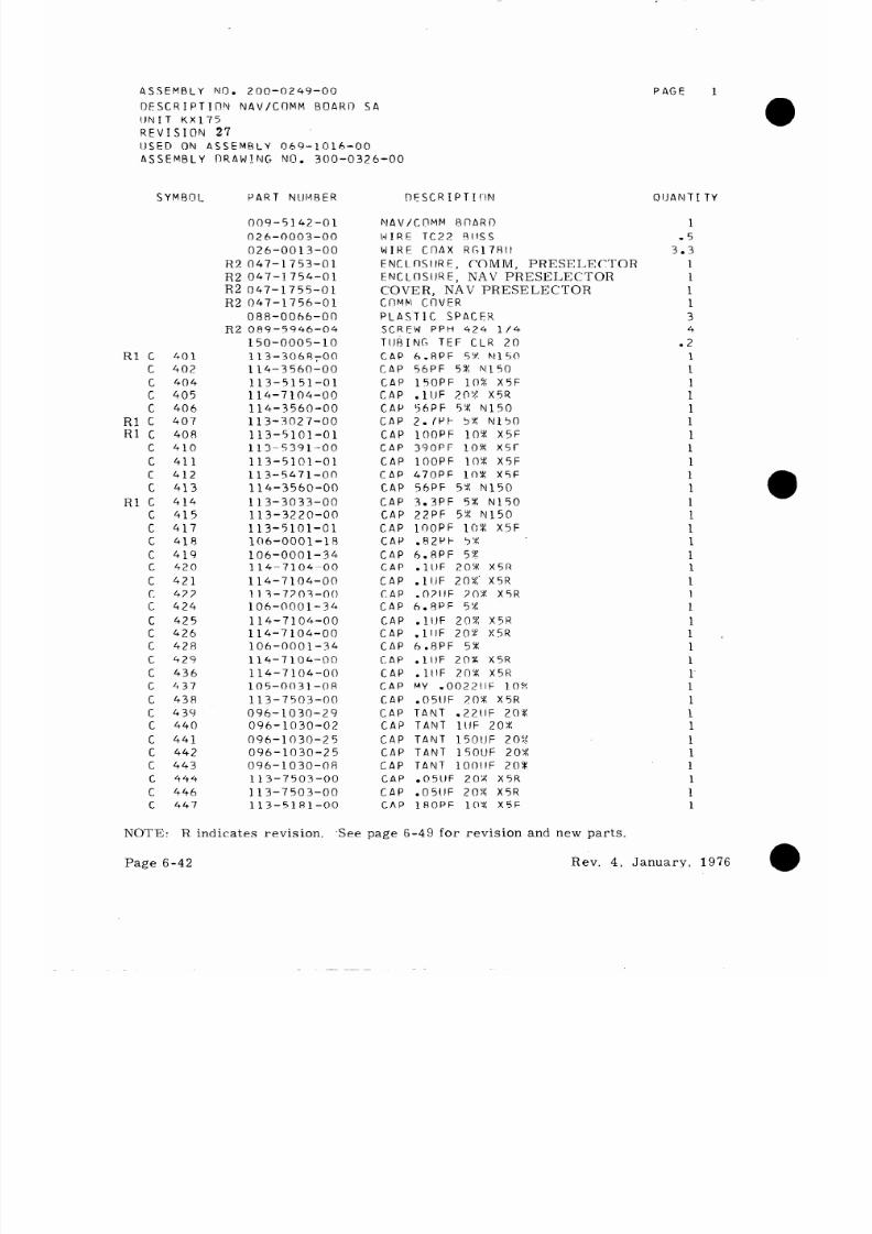
8/9/2019 KX 170A - Maintenance Manual Honeywell
http://slidepdf.com/reader/full/kx-170a-maintenance-manual-honeywell 272/586
ASSEMBLY NO. 200-0249-00
DESCRIPTION NAV/COMM BOARD SA
(JNIT KX175
REVISION 27
IJSED DN ASSEMBLY 069-1016-00
ASSEMBLY
SYMBOL
Rl C 401
c 402
C 404
C 405
C 406
Rl C 407
Rl c 408
C 410
C 411
C 412
C 413
Rl C 414
C 415
C 417
C 418
C 419
C 420
C 421
C 422
C 424
C 425
C 426
C 428
C 429
C 436
C 437
C
43R
C 439
C 440
C 441
C 442
C 443
C 444
C 446
C 447
DRAW NG NO.
300-0326-00
PART NUMBER
DFSCRIPTION OIJANTITY
009-5142-01
t'JAV/COMM RnARD
1
026-0003-00 WIRE TC22 SltSS .5
026-0013-00
WIRE COAX RG17811
3.3
R2 047-1753-01
ENCLnStJRF, COMM, PRESELECTOR 1
R2 047-1754-01
ENCLnSlJRE,
NAV PRESELECTOR 1
R2 047-1755-01
COVER, NAV PRESELECTOR
1
R2 047-1756-01
CflMM COVER
1
088-0066-00
PLASTIC SPACER 3
R2 089-5946-04
SCREW PPH 424
l/4
4
150-0005-10
TURING TEF CLR 20
.2
113-306Rr00
CAP h.RPF 5%
Ml50
1
114-3560-00
CAP 56PF 54: Nl.50
1
113-5151-01
CAP 150PF 10X X5F
1
114-7104-00
CAP .
1IJF 20X X5R
1
114-3560-00 CA -) 56PF 5‘# N150
1
113-3027-00 CAP 2.7PF 5X N150
1
113-5101-01
CAP 1OOPF
10%
X5F
1
113-5391-00 CAP 390PF 10X X5F
1
113-5101-01
CAP 1OOPF 10X X5F
1
113-5471-00 CAP 470PF 10X X5F
1
114-3560-00 CAP 56PF 5'x N150
1
113-3033-00
CAP 3.3PF 5X N150
1
113-3220-00 CAP 22PF 5x N150
1
113-5101-01
CAP 1OOPF 10% XSF
1
106-0001-18 CAP
.FI2PF 5°C:
1
106-0001-34
CAP h.RPF 5%
1
114-7104-00 CAP .
1OF 20x X5R
1
114-7104-00 CAP
.lIJF 20% X5R
1
113-7203-00 CAP
.02ttF 20X X5R
1
106-0001-34
CAP h.SPF 5X
1
114-7104-00 CAP .
1IJF 20% X5K
1
114-7104-00
CAP
.lIIF 20X X5R
1 ,
106-0001-34
CAP h.RPF 5X
1
114-7104-00 CAP .
1llF 20X X5R
1
114-7104-00
CAP .
1llF 20X X5R
1
105-0031-08
CAP MY .0022llF
10%
1
113-7503-00 CAP
.051JF 20X X5R
1
096-1030-29
CAP TANT .22(IF 20.X
1
096-1030-02
CAP TAh T
1lJF 20x
1
096-1030-25
CAP TANT 1501JF 20:2
1
096-1030-25
CAP TANT 1501JF 20X
1
096-1030-08
CAP TANT 1OOlJF 20X
1
113-7503-00
CAP
.051JF 20X X5R
1
113-7503-00
CAP
.05(lF 20X X5R
1
113-5181-00 CAP 1ROPF 10X X5F
1
NOTE: R indicates revision.
,See page 6-49 for revision and new parts.
PAGE 1
0
Page 6-42
Rev. 4, January, 1976
0

8/9/2019 KX 170A - Maintenance Manual Honeywell
http://slidepdf.com/reader/full/kx-170a-maintenance-manual-honeywell 273/586
ASSEMBLY NO. 200-0249-00
OESCRIPTI~N NAV/CnMM BOARD SA
IJNIT KX175
REVISIflN 27
USED ON ASStMBLY @69-1016-00
ASSEMBLY
SYMBOL
c
448
c
449
c
450
C
451
C
452
C
453
C
454
C
455
C
456
c
457
C
458
c
459
c 460
C
461
c
462
C
463
c
464
c
465
C
466
C
467
c
468
c
469
C
470
c
472
c
473
c
474
C 475
c
476
c
477
c
478
C
479
c
680
Rl C
481
C
482
c
483
Rl C
484
c
485
C
486
Rl C
487
C
488
C
4R9
C
490
R1 c
491
c
492
C
493
DRAWING NO.
300-0326-00
PART NOMBER QlJANTI TY
113-3330-00 CAP
33PF 5X N150 1
113-7503-00
CAP
.05tIF 202 X5R 1
114-7104-00
CAP
.lUF 20% X5R
1
114-7104-00
CAP
.lIJF 20X X5R
1
096-1030-24
CAP
TANT 6HlJF 20x 1
096-1.030-17
CAP
TANT 6.HIJF 20x
1
114-7104-00 CAP
.lIlF 20x X5R
1
105-0031-47
CAP
MY .0271JF lo’%
1
114-7104-00
CAP
.lIJF 20X X5R
1
096-1030-03
CAP TANT 2.21lF 10X
1
113-7503-00
CAP
.05LJF 20X X5R
1
114-71OL-00
CAP
.lIlF 20X X5R
1
113-5331-00
CAP 330PF 10% X5F
1
114-7104-00
CAP .lIIF 20X X5R
1
114-7104-00
CAP
.l )F 20X X5R
1
113-3270-00 CAP 27PF 5X N150
1
096-1030-17
CAP
TANT 6.f (JF 20X
1
096-1030-02
CAP
TANT lI F 20X
1
096-1030-02 CAP TANT 1IJF 20X
1
113-3039-00
CAP
3.9PF 5X N150
1
113-3820-00 CAP 82PF 5’1: X5F
1
113-3047-00
CAP
4.7PF 5X N150
1
113-5151-01
CAP
150PF
10x: X5F
1
114-7104-00
CAP .ltJF 20X X5R
1
113-5151-01
CAP
150PF
10% X5F
1
113-5022-00
CAP 2.2PF N150
1
113-3390-00
CAP 39PF 5X N150
1
113-5471-00 CAP 47OPF
10x X5F
1
113-5471-00
CAP
470PF
10% X5F
1
113-5151-01 CAP
15OPF
10X X5F
1
113-5151-01
CAP
150PF 10x: X5F
1
113-5151-01
CAP
15OPF 10X X5F
1
113-3033-00 CAP 3.3PF 5x iv150 1
113-3390-00
CAP
39PF 5% I1150
1
113-5101-01 CAP
ICOPF lO”A: X5F
1
113-3120-00
CAP
17PF 5% lU150
1
114-7104-00
CAP
.lllF 20X X5R
1
114-7104-00 CAP .llJF 20% X5;7
1
113-3120-00 CAP 12PF 5X N15O
1
114-7104-00 CAP
.lIlF 20x X5R
1
114-7104-00
CAP
.llJF 202 X5R
1
113-7203-00
CAP .021JF 20X X5R
1
113-3120-00 CAP
12PF 5% Nl50
1
114-7104-00
CAP
.lIJF 20X X5K
1
11
4-7
104-00
CAP
.lIIF 20X X5R
1
NOTE: R indicates revision.
See page 6-49 for revision and new parts.
Rev. 4, January, 1976
PAGE 2
Page 6-43

8/9/2019 KX 170A - Maintenance Manual Honeywell
http://slidepdf.com/reader/full/kx-170a-maintenance-manual-honeywell 274/586
ASSEMBLY Nfl. 200-0249-00
DESCRIPTION NAV/CDMM BDARD SA
UNIT KX175
REVISION 27
USED ON ASSEMBLY 069-1016-00
PAGE 3
a
ASSEMBLY
DRAWING ND.
300-0326-00
SYMBOL PART NJJMRER
c
494
114-7104-00
CAP
.lUF 20x X5R
c 495
096-1030-27
CAP TANT 15ilF 20X
c 496 105-0031-32
CAP MY
.OlUF 10%
C 497
096-1030-27 CAP TANT 15lJF 2OW
C 498
096-1030-02 CAP TANT lI F 20X
C
49Y
096-1030-02
C4P TANT 1UF 204:
C
501 114-7104-00
CAP
.lJJF 20"' X5R
c
502
105-0031-35 CAP MY
.012lJC 10%
c 503
105-0031-32
CAP MY
.OliJF 10X
C 504
113-3B20-00
CAP R2PF 5% X5F
Rl c 505
096-1030-02
CAP TANT 1lJF 20%
C 506
114-7104-00
CAP
.llJF 20% X5.R
C 507
113-7203-00 CAP . 02UF 20% X5R
c 508
096-1030-27
CAP TANT 15 JF 20x
c 509
096-1030-02 CAP TANT 1JJF 20%
C 510
113-7203-00
CAP
.02lJF 20% X5R
c 511
096-1030-02
CAP TANT 1lJF 20x
C 512
096-1030-21 CAP TANT 12JJF 20X
CJ 401
026-0015-00
CIRCkJIT JlmJ*JPFR
CR 401
007-4012-00
nInnE SMV626
CR 402 007-4012-00
OInDE SMV626
CR 403
007-4012-00 nI DDE SJ".,V626
CR 404 007-6067-00
l:,IflrJE MRD 101
CR 405
007-6067-00
DIOI?F MRD 101
CR 406
007-6067-00
DInnE MYo 101
CR 407
007-6067-00
DIODE MB , 101
CR
408 007-5011-05
DIrlDE ZEh FR 3.3V
CR 409
007-6035-00 DIflnF lhl8lh
R4
CR 410
007-6035-00
DIODE lh;F(lh
CR 411
007-6029-00 DIODE SIL ll\J457
CR 412
007-6029-00 DIODE
SIL lit1457
CR 413
007-5011-13
DIODE ZFNER 5.6V
CR 414
007-5011-1~
OIDDE ZFNFR 6.HV
CR 416
007-4012-00 DI
DDF SMV626
CR 417
007-4012-00
PlIflDE SI*'V626
CR 418
007-LO12-00
T)IrlnE S”lVh2h
CR 419
007-4012-00
D I Cl
D F S J:'V 6 2 6
CR 420
007-6067-00
DIODE MBD 101
CR 421
007-6067-00
DIOOE YR ) 101
CR 422
007-6067-00
T?Ill?F MBD 101
CR 423
007-6067-00 DIODE Mt3D I.01
CR 424
007-5011-05 DIODE ZFh’Ffi 3.3\/
Rl CR 425
007-6045-00
DI DDE FH 1100
R4
CR 426
007-6035-00
DIDDF lh1516
CR 427
007-6029-00
DIDI?E SIL lN457
OJJANTITY
1
1
1
1
1
1
1
1
1
1
1
1
1
1
1
1
1
1
1
1
1
1
1
1
1
1
1
I.
1
1
3
1
1
1
1
1
1
1
1
1
1
1
1
1
. 1
NOTE: R indicates revision.
See page 6-49 for revision and new parts,
Page 6-44
Rev. 4, January, lY76

8/9/2019 KX 170A - Maintenance Manual Honeywell
http://slidepdf.com/reader/full/kx-170a-maintenance-manual-honeywell 275/586
ASSEMBLY NC). 200-0249-00
DESCRIPTIDN NAV/COMFq BDARl1 SA
UNIT KX175
REVISIflN 27
IJSED ON ASSEMRLY 069-1014-00
ASSEMBLY
DRAWING Nn. 300-0326-00
SYMBOL PART NIIMBER DESCRIPTIllN
Rl
CR 428 007-6016-00
CR
429 007-6016-00
CR
430
007-602 l-00
CR
431
007-6029-00
CR
432 007-5011-13
FL
401 017-0035-00
FL
402
017-0035-00
FL
403
017-0034-00
I
401
120-3007-00
I
402
120-3007-00
I
403
120-3006-00
I
404
120-3007-00
I
405
120-3007-00
Rl I-
401 019-2150-00
Rl L 402
019-2057-16
Rl L
403
019-2150-01
L
404
019-2054-20
Rl
L
405
019-2150-01
L
406 019-2109-00
L
407
019-2150-02
L
408
019-2057-15
L
409 019-2150-03
L
410
019-2054-19
L
411 019-2150-04
L
412
019-2057-$8
L
413
019-2150-05
L
414
019-2109-00
L
415
019-2082-70
R2 0 401 007-0093-00
R2 0
403 007-0196-00
R2 0
404 007-0119-00
0
405
007-0075-00
0
406
007-0078-00
R2 0
407
007-0119-00
(3
408 007-0195-00
0
409
007-0195-00
0
410
007-0078-00
R2 0
411
007-0093-00
R2 0
413 007-0196-00
R2 0
414
007-0119-00
0
415 007-0078-00
R2 o
414
007-0119-00
0 417 007-0078-00
0
418 007-0078-00
0
419 007-0078-00
DIODE SIL
lN4154
DI(IDE SIL lN4154
PIODE l-s-2
DIODIF SIL 1n1+57
DInP,E ZENER 5.6V
FILTER 15.1875MHZ
FILTER 15.1875MHZ
FILTER 9.000MHZ
INT CKT lJRR7703394
IRlT CKT llBR7703394
INT CKT CA3020
INT CKT 11887703394
II\IT
CKT lJRR7703394
CHOKE RF
CHOKF 2.21JH 5X
CHOKE RF
CHOKE 2.2tJY 5X
CHOKE RF
INDllCTl-lR \/AR I
CHnKE RF
CHOKE 1.RIIt-l 5%
CHOKE RF
CHOKE 1.81JH 5X
CHflKF RF
CHCIKF 3.31lH 5%
CHflKE RF
INDLJCTIJR VAR I
CHnKE 240lJH 5X
TRANS I STnR SK7905
TRANS I STC R MPSH20
TRANS
I
STnR 2N49 17
TRANS I STDR 2N3415
TRANSISTnR 2N3415
TRANSISTCIR ZN4917
TRAl\‘S I STnR MPSHlO
TRANSISTOR MPSHlO
TRANS
I
STnR 2N343 5
TRANSISTnR SK7905
TRANS I STnR MPSH20
TRANSISTnR 2N4917
TRANSISTOR 2N3415
TRANSISTflR 2N4917
TRANS
I
STOR 2N3415
TRANSISTOR 2N7415
TRANS ISTnR 21\ 3415
PAGE 4
3UANTI TY
1
1
1
1
1
1
1
1
1
1
1
1
1
1
1
1
1
1
1
NOTE: R indicates revision.
See page 6-49 for revision and new parts.
Rev. 4, January, 1976
Page 6-45

8/9/2019 KX 170A - Maintenance Manual Honeywell
http://slidepdf.com/reader/full/kx-170a-maintenance-manual-honeywell 276/586
ASSEMBLY ND. 200-0249-00
0ESCRIPT
ION
NAV/COMM BDARI) SA
IJNIT
KX175
REVISInN
27
c SED f-IN ASSEMRLY 069-1016-00
ASSEMBLY DRA’* ING N@. 300-0326-00
SYMBOL
Q 420
t R 401
R 402
R 403
R 404
9 405
R 406
R 407
R 408
R 409
R 410
R 413
R 414
R 415
R 417
R 421
R 422
R 424
R 425
R 426
R 427
R 428
R 429
R 430
R 431
R 432
R 433
R 434
R 435
R 436
R 437
R 438
R 439
R 440
R 441
R 442
R 443
R 444
R 445
R 446
R 447
R 445
R 449
R 450
R 451
PART NIJMBER
DESCRIPTIOY
007-0078-00 TRANSISTnR 2N3415
130-0103-25 RES lr)K 10X QW
130-0103-25 RES 10K lOX,OW
130-0102-23
RES 1K 5% OW
130-0622-23 RES 6.2K
10% Oh
130-0621-23
RFS 620flHM 5% OW
130-0101-25
RES 100 10X Oh
130-0103-25 RES 1OK 104 OW
130-0473-23 RES 47K 5X 0W
130-0683-23 RFS 68K 5X OW
130-0222-23 RES 2.2K 5X (3W
130-0131-23 RF-S 130 5X OW
130-0132-23 RES 1.3K 5X OW
130-0332-23
RFS 3.3K 5X O nl
130-0473-23
RES 47K 5X (3W
130-0103-25
RES 10K 10X Old
130-0473-23
RES 47K 5X OW
130-0201-23
RES 200 5X Ow
133-0084-01’
RES VARI 5K
130-0471-25
RES 470
10% 0W
130-0112-23
RES l.lK 5X O\d
130-0242-23 RES 2.4K 5X 0W
130-0103-23
RES 1OK 5X (3W
130-0222-23 RES 2.2K 5X OW
130-0223-23
RES 22K 5% OW
130-0223-23
RES 22K 5% OW
136-1741-77 RES 1.74K 1% OW
136-1211-77 RES 1.21K 1X OW
130-0181-23
RES
180 5x QW
130-0222-25 RES 2.7K
10%
C3W
130-0331-23
KES 330 5% ow
130-0101-25
RES 100 10% OW
130-0101-25 RES
100 10X Ow
130-0512-23 RES 5.2K 5X OW
130-0133-23
RES 13K 5% OW
130-0472-2 3
RES 4.7K 5X OW
130-0332-23
RES 3.3K 5X Oh
130-0300-33
RES 30 5% HW
130-0224-25 RES 220K 10% 0W
130-0224-2 5
RES 220K
10X OW
130-0152-25
RES 1.5K 10% O d
130-0751-23 RES 750 5X OW
130-0182-23
RES l.BK 5X OW
130-0224-23
RES 220K 5% (3W
130-0472-23 RES 4.7K 5X OW
PAGE 5
0
OIJANTITY
1
1
1
1
1
1
1
1
1
1
1
1
1
1
1 ’
NOTE: R indicates revision.
See page 6-49 for revision and new parts.
Page 6-46
Rev. 4, January, 1976

8/9/2019 KX 170A - Maintenance Manual Honeywell
http://slidepdf.com/reader/full/kx-170a-maintenance-manual-honeywell 277/586
ASSEMBLY h10. 200-0249-00
')ESCRIPTION b~AV/CU~MM BI1ARI1 SA
IJNIT KX175
REVISInN
27
IJSED ON ASSFMRLY 069-1016-00
A'SSEMRLY
S Y c.1 0 L
Rl R
452
R '4.5 3
R 454
R 455
R 456
R 457
R 458
R 460
R 461
R 462
RI Fi
463
R 464
R 465
R 466
R 467
R2 R
468
Rl a
469
R 470
Rl R
471
Rl R
472
R 473
Rl
R 474
Rl R
475
R 4 7 6
Rl R
477
Rl R 478
R 479
R 481
R 482
R 483
R 484
R 455
R 486
R
4R7
R 488
R 489
R 490
R 491
R 492
R 493
R 494
R 495
R 496
R 497
R 498
DRAWING NO.
300-0326-00
PART NIJMSFR DESCRIPTInN
130-0332-23
RES 3.3K 5% O'd
130-0133-23
RES 13K 5% Old
130-0512-23
RES 5.2K 5x OhI
130-0101-25 RES 100 10% 0C'
130-0470-25
RES 47 10X OW
130-0102-23
KES 1K 5% c3W
130-0753-23
RES 75K 54 OW
130-0103-25 RES 1OK
10X
13W
130-0103-25
RFS
1OK 10X
OW
130-0102-23
RES
1K 5X 014
130-0621-23
RES h2OnHM 5% 014
130-0682-23
RES 6.8K 5X OhI
130-0101-25 RES 100 10X OW
130-0103-25 RES 10K 10X Oh
130-0103-25 RES 10K
10X 04
130-0473-23
RES 47K 5% OW
130-0753-23
RFS 75K 5% OW
130-0222-23 RFS 2.2K 5% OW
130-0102-23
RFS 1K 5X O’*I
130-0563-23 RES 56K 5% OM
130-0131-23
RFS 130 5% Oh
130-0132-23
RES 1.3K 5% OW
130-0332-23 RES 3.3K 5X OhI
130-0472-23
RES 4.7K 5% ISkl
130-0393-23
RFS 3YK 5% OW
130-0104-23 RES
1OOK 5X
0W
130-0472-23 RES &.7K 5% OhJ
130-0103-25
RES 10K 10% 0kf
130-0330-23
RES 330HM 5x OW
133-0084-02 RFS VARI 10K
130-0181-23
RFS 180 5X Old
l?O-0681-23
RES 6ROOHM 5% Old
130-0391-23 RES 3900HM 5M Old
130-0473-25 RES 47K 10X (3W
130-0103-23 RES 1OK 5% QW
130-0472-23
RFS 4.7K 5% OW
130-0152-23 RFS 1.5K 5% OW
130-0222-25 RES 2.2K
10X
OW
130-0472-23
RES 4.7K 5% OW
130-0331-23 RES 330 5% OW
130-0621-23 RES 620nHM 5% QW
133-OOA4-00 RES VARI 1K
130-0182-23
RFS l.RK 5% OW
130-0151-25
RES 180 10% (3W
130-0473-25
RES 47K 10% OW
NOTE: R indicates revision.
See Page 6-49 for revision and new parts.
Rev. 4, January, 1976
PAGE 6
O JANTI TY
1
1
1
1
1
1
1
1
1
1
1
1
Page 6-47

8/9/2019 KX 170A - Maintenance Manual Honeywell
http://slidepdf.com/reader/full/kx-170a-maintenance-manual-honeywell 278/586
ASSEMBLY NO. 200-0249-00
DESCRIPTION NAV/COMM ROARD SA
UN1 T KXl75
REVISION 27
IISFD I-IN ASSEMBLY 069-1016-00
ASSFMHLY
SYYROL
R 499
R 500
R 502
R 5’03
R 504
K 505
R 506
R 507
R 508
R 509
RT 501
RT 502
Rl
T 40 1
Rl T
LO2
Rl
T 403
T 404
T 405
T 404
T 4137
T 408
T 409
T 410
T 411
T 412
T 413
T 414
T 415
R1 T 416
Rl T 4 1 7
RI T
418
Rl
T 419
T
E: T
420
42 1
Y 401
Y 402
DRAWING NO. 300-0326-00
PART NiJMRER
DESCRIPTION
130-0101-25
RES 100 10X (3W
130-0102-25
RES 1K 10X OW
130-0471-25 KES 470 10X 0W
130-0101-25
RES 100 10X OhI
130-0182-23
RES 1.8K 5% Old
130-0102-25
RES 1K 10X OW
130-0103-23
RES 10K 5X OW
130-0103-23
RES 1OK 5X Old
130-0332-23
RFS 3.3K 5X O\d
130-0103-23
RES 10K 5% rSW
134-l 004-00
THERMISTOR 1K
134-1019-00 THERM1 STOR 50
019-5056-04 TRANSFORMER MIXER
019-5056-03 TRANSFflRMER MI XFR
019-8044-00 TRA~~SFf~RMER
IF
019-8044-01 TRANSFORMER IF
019-8034-03 TRANSFnRMER
IF
019-8034-04 TRANSFIIRMEK
I
F
019-8034-01
TRANSFORl’-lER IF
019-8034-01
TRANSFt-lRMF?
I
F
019-80~5-00 TRAhiSFflRMER
IF
n19-8034-01
TRANSFORMFR I F
019-5055-00 TRANSFflRMER AIJDIPI
019-5056-05 TRANSFORMER MIXER
019-5056-04
TRANSFOKMFR MIXER
OlY-8043-01 TRANSFORMER IF
0 19-8043-00
TRANSFflRMFR
IF
019-5034-02
TRANSFORMER
IF
019-8034-05
TRANSFORMER
IF
019-5034-00
TRANSFORMFR
IF
019-8034-00
TRANSFORMER IF
019-8034-00
TRANSFORMER
I
F
019-8034-00
TRAb SFflRMFR IF
044-0029-01 XTAL
14.OOlRMHZ
044-0029-00
XTAL 8.13875MHZ
PAGE 7
a
OIJANTI TY
1
1
1
1
1
1
1
1
VOTE: R indicates revision.
See page 6-49 for revision and new parts.
Page 6-48
Rev. 4, January, 1976

8/9/2019 KX 170A - Maintenance Manual Honeywell
http://slidepdf.com/reader/full/kx-170a-maintenance-manual-honeywell 279/586

8/9/2019 KX 170A - Maintenance Manual Honeywell
http://slidepdf.com/reader/full/kx-170a-maintenance-manual-honeywell 280/586

8/9/2019 KX 170A - Maintenance Manual Honeywell
http://slidepdf.com/reader/full/kx-170a-maintenance-manual-honeywell 281/586

8/9/2019 KX 170A - Maintenance Manual Honeywell
http://slidepdf.com/reader/full/kx-170a-maintenance-manual-honeywell 282/586
KI G
r
X 170A KX 175
NAVIGATION RECEIVER/
COMMUNICATIbNS TFtANSCEIVER
R440
R408
R443
R441
R409
R410
R439
R492
R415
R414
R413
R450
R417
R447
R448
R446
R407
R44 5
R406
R405
R449
R404
R403
R444
R422
R402
R421
R424
R401
R425
R426
R437
R435
R433
R438
R431
R428
R434
R432
R436
R427
R429
R430
Page 6-52
FIGURE 6-7B NAV/COMM BOARD SUB-ASSEMBLY
(Dwg. No. 696-6099-00)
Rev. 2, December, 1972

8/9/2019 KX 170A - Maintenance Manual Honeywell
http://slidepdf.com/reader/full/kx-170a-maintenance-manual-honeywell 283/586
KI G
7
X 170A
KX 175
NAVIGATION RECEIVER /
COMMUNICATIONS TRANSCEIVER
FIGURE 6-7C NAV/COMM BOARD SUB-ASSEMBLY
(Dwg. No. 696-6100-00)
Rev, 2, December, 1972
Page 6-53

8/9/2019 KX 170A - Maintenance Manual Honeywell
http://slidepdf.com/reader/full/kx-170a-maintenance-manual-honeywell 284/586
ASSEMBLY’NO. 200-0083-00
DESCRIPTION TRANSMITTER ASSY
UNIT KX175
REVISION 11
USED ON ASSEMBLY 200-0082-00
PAGE 1
ASSEMBLY
DRAWING NO.
300-0106-00
SYMBOL PART NUMBER
DESCRIPTION QUANTI TV
c 601
Rl c 602
C 603
C .604
C 605
c 606
C 607
C 608
Rl C 609
C 610
C 613
C 614
C 615
C 616
C 617
c 618
C 619
C 620
C 621
C 622
C 628
C 629
CR 601
CR 602
L 601
Rl 0 601
R 601
R 602
R 603
R 604
Rl R 605
R 606
Rl R 607
R 608
R 609
R 610
R 611
R 613
R 614
R 615
R 618
T 601
T 602
009-5075-00
PC BOARD
1
150-0042-10
TUBING SHRINKABLE
.2
113-5471-00 CAP 470PF 10% X5F
1
113-3068-00
CAP 6.8PF 5% N150
1 ’
113-5471-00 CAP 470PF 10% X5F
1
113-3120-00
CAP 12PF 5% N150
1
113-5151-01
CAP 150PF 10% X5F
1
106-0034-00 CAP FT 1.5KPF 20%
1
113-6103-00
CAP
.OlUF 20% X5F
1
106-0034-00 CAP FT 1.5KPF 20%
1
113-3270-00
CAP 27PF 5% N150
1
102-0024-09
CAP VARI 7-35PF
1
113-6103-00 CAP .OlUF 20% X5F 1
113-6103-00
CAP .OlUF 20% X5F
1
106-0034-00 CAP FT 1.5KPF 20%
1
113-3820-00 CAP 82PF 5X X5F
1
113-3820-00
CAP 82PF 5% X5F
1
113-3680-00
CAP 68PF 5% X5F
1
102-0024-09
CAP VARI 7-35PF
1
113-6103-00 CAP .OlUF 20% X5F
1
106-0034-00 CAP FT 1.5KPF 20X
1
102-0024-09 CAP VARI 7-35PF
1
113-6103-00
CAP
.OlIJF 20% X5F
1
113-3180-00
CAP 18PF 5% N150
1
007-6022-00
DIODE TS6
1
007-6022-00 DIODE TS6 1
019-2057-11
CHOKE
.82UH 5%
1
007-0134-00 TRANSISTOR SE3005
1
130-0392-25
RES 3.9K 10% QW
1
130-0472-2 5
RES 4.7K 10% QW
1
130-0271-25
RES 270 10X QW 1
130-0470-25 RES 47 10% OW
1
130-0472-25 RES 4.7K 10% QW
1
130-0471-25 RES 470 10X QW
1
130-0039-25 RES 3.9 10% QW
1
130-0180-35 RES 18 10% HW
1
130-0511-33 RES 510 5’% HW
1
130-0511-33
RES 510 5% HW
1
130-0680-35 RES 68 10% HW 1
130-0391-25
RES 390 10% QW
1
130-0750-33 RES 75 5% HW
1
130-0300-33
RES 30 5% HW
1
130-0510-23 RES 51 5% OW
1
019-3044-00 TRANSFORMER RF
1
019-3026-00
TRANS BIFILAR WND
1
NOTE: R ind
ica
t
es revis ion.
See page 6-56 for revision and new parts.
Page 6-54.
Rev. 2,. December, 1972

8/9/2019 KX 170A - Maintenance Manual Honeywell
http://slidepdf.com/reader/full/kx-170a-maintenance-manual-honeywell 285/586
ASSEMBLY NO. 200-0083-00
DESCRIPTI‘ON TRANSMITTER ASSY
UNIT KX175
REVISION 11
USED ON ASSEMBLY 200-0082-00
ASSEMBLY DRAWING NO. 300-0106-00
SYMBOL PART NUMBER
DESCRIPTION
T
603 019-3026-00
TRANS BIFILAR WND
NOTE: R indicates revision.
See page 6-56 for revision and new parts.
Rev. 2, December, 1972
PAGE 2
OUANTI TY
1.
Page 6-55
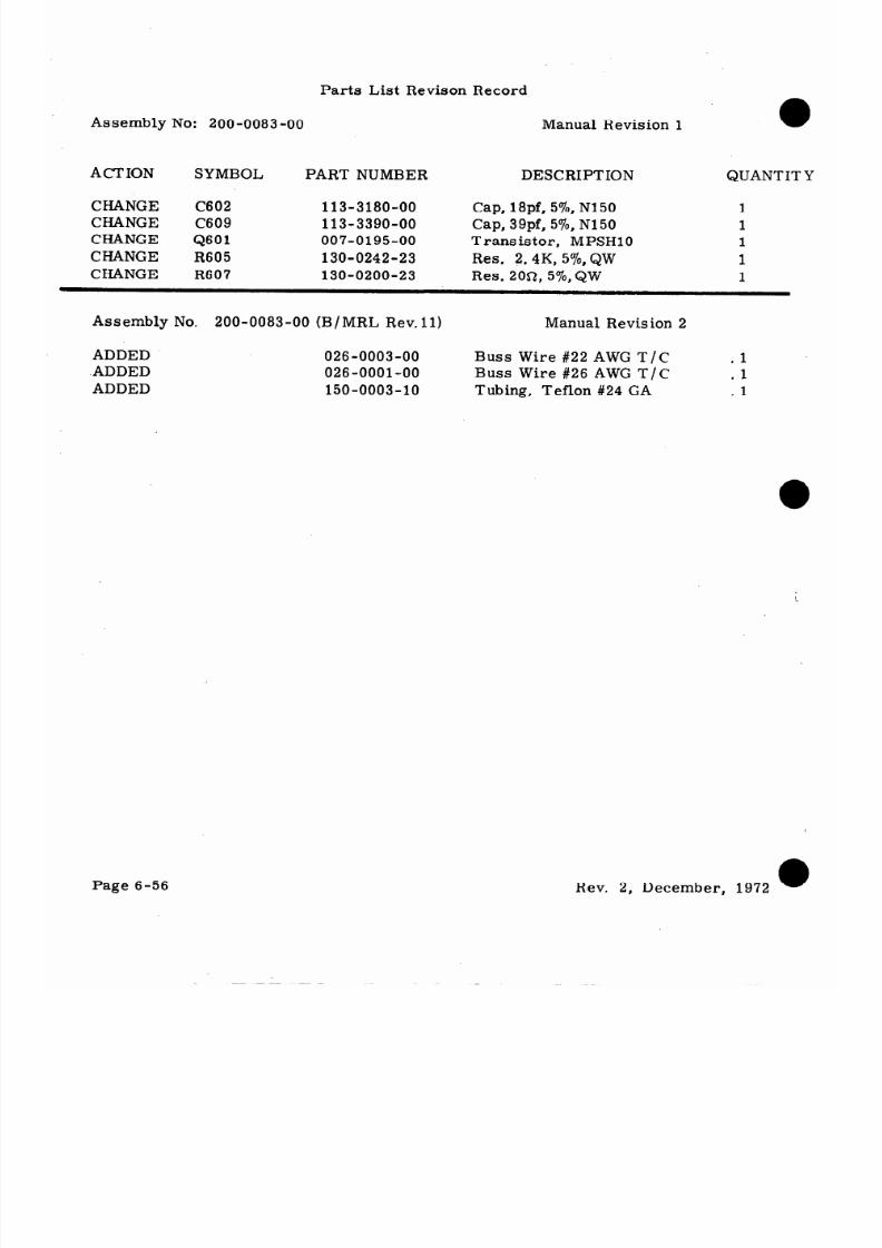
8/9/2019 KX 170A - Maintenance Manual Honeywell
http://slidepdf.com/reader/full/kx-170a-maintenance-manual-honeywell 286/586
Parts List Revison Record
Assembly No: 200-0083 -00 Manual Revision 1
ACTION SYMBOL
PART NUMBER DESCRIPTION QUANTITY
CHANGE
C602
113-3180-00
Cap, 18pf, 5%, N150
1
CHANGE C609 113-3390-00
Cap, 39pf, 5%, N150 1
CHANGE Q601
007-0195-00
Transistor, MPSHlO
1
CHANGE R605
130-0242-23
Res. 2.4K, QW
70, 1
CHANGE
R607
130-0200-23 Res. 200,
5770,
QW 1
Assembly No.
200-0083-00 (B/MRL Rev. 11)
Manual Revision 2
ADDED
ADDED
ADDED
026-0003-00
Buss Wire #22 AWG T/C
.l
026-0001-00 Buss Wire #26 AWG T/C .l
150-0003-10 Tubing, Teflon #24 GA
.l
Page 6-56
Rev. 2, December, 1972
l

8/9/2019 KX 170A - Maintenance Manual Honeywell
http://slidepdf.com/reader/full/kx-170a-maintenance-manual-honeywell 287/586
C602
C603
Q601
R603
R628
c601
R607
C606
C604
C608
T602
R611
c610
C609
R613
T603
C619
C618
C616
C617
C622
KI G
KX 170A
7
X 175
NAVIGATION RECEIVER/
COMMUNICATIONS TRANSCEIVER
C607
R608
CR601
,C613
'CR602
'R614
,L601
696-6101-00
FIGURE 6-8 TRANSMITTER ASSEMBLY
(Dwg. No. 696-6101-00)
Rev. 2, December, 1972
Page 6-57

8/9/2019 KX 170A - Maintenance Manual Honeywell
http://slidepdf.com/reader/full/kx-170a-maintenance-manual-honeywell 288/586
ASSEMBLY NO. ZOO-OOR2-00
DESCRIPTION REAR PLATE ASSY
1JNIT KX175
REVISION 12
USED ON ASSEMBLY 069-1016-00
ASSEMBLY DRAWING ND. 300-0105-00
PAGE 1
a
SYMBOL
008-0042-00 LUG SOLDER
008-0044-01
TERM DBL END
010-0019-90 TERM STANDOFF WHT
010-0029-90 TERM FEED THRIJ WHT.
016-1004-00 THERMAL COMPDIJND
026-0003-00 WIRE TC22 BJJSS
.l
047-1833-01
CONNECTnR COVEK
1
073-0093-02
REAR PLATE
R4
076-0164-06
SPACER
089-2005-37 NUT STOP 2-56
089-2272-30 NIJT HEX B-32
089-5874-03
SCR PHP 2-56X3/16
089-5878-04 SCR PPH 4-40X1/4
089-8012-37
LOCK WASHER INT 2
OYO-n133-00
HEAT SINK
1
091-0028-00
SCK NYPH 4-40X3/16
1
091-0069-36
WASHER MICA
1
106-0006-02
CAP FT 22PF 10x
1
113-5221-01
CAP 220PF 10% X5F
1
106-0006-03
CAP FT 250PF 20X
1
106-0006-00
CAP FT 33PF
10%
1
106-0006-00
CAP FT 33PF 10%
1
106-0024-00
CAP STANDOFF 2OPF
1
113-3200-00
CAP 20PF 5X N150
1
007-6059-00 DIODE FD400
007-6059-00 D I
ODE FD400
1
017-0025-00
FILTER
017-0027-00 FILTER
017-002.f-00
FILTER
030-0059-00
CflNNECTDR ANT FFM
030-0059-00
C TNNFCTOR ANT FFM
019-2054-17
CHOKE 1.21JH 5%
007-0066-00 TRANS I STDR 2N3R66
007-0149-00
TRANSISTOR SS 3932
OO7-0150-(10
TRANSISTflR SS 3933
130-0068-33
RES 6.8 5X HW
130-0222-25
RES 2.2K
10X OW
130-0471-35
RES 470
10%
HW
019-3045-00
TRANSFURMER RF
Rl
c 624
C 625
c 626
C 627
C 629
C 631
C 632
CK 603
CR 604
FL 601
FL 602
FL 603
J 172
J 173
L
604
(3 602
0 603
Q 604
R 612
K 616
R 617
T
604
PART NIJMBER
DESCRIPTION
NOTE: R indicates revision.
See page 6-59 for revision and new parts,
OUANTI TY
Page 6-58
Rev. 4, January, 1976

8/9/2019 KX 170A - Maintenance Manual Honeywell
http://slidepdf.com/reader/full/kx-170a-maintenance-manual-honeywell 289/586
Parts List Revision Record
Assembly No: 200-0082-00
Manual Revision 1
ACTION
SYMBOL
PART NUMBER
DESCRIPTION
QUANTITY
CHANGE 091-0155-00 Washer, Mica 1
Assembly No. 200-0082-00 (B/MRL Rev. 12)
Manual Revision 4
CHANGE
076-0164-06
Spacer
3
ADDED
076-0139-09
Spacer
1
R,ev. 4, January, 1976
Page 6-59

8/9/2019 KX 170A - Maintenance Manual Honeywell
http://slidepdf.com/reader/full/kx-170a-maintenance-manual-honeywell 290/586
FL602
c629
FL601
~624
c623
C632
C612
NAVIGATION R;ECEIVE$/
COMMUNICATIONS TRANSCEIVER
a
cR604
L604
c627
CR603
T604
4604
R612
4603
c611
4602
FIGURE 6-9 REAR PLATE
(Dwg. No. 696-6102-00)
Page 6’60’: ,..
R6,i6 ,i
C625
FL603
C631
R617
C626
5172
5173
Rev. 2;’ December, 1,972
e
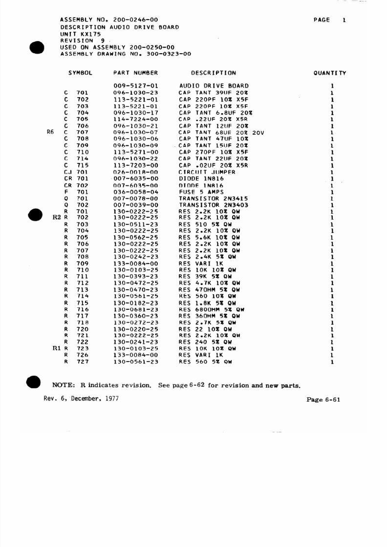
8/9/2019 KX 170A - Maintenance Manual Honeywell
http://slidepdf.com/reader/full/kx-170a-maintenance-manual-honeywell 291/586
ASSEMBLY NO. 200-0246-00
DESCRIPTION AUDIO DRIVE BOARD
UNIT KX175
PAGE 1
REVISION 9
USED ON ASSEMBLY 200-0250-00
ASSEMBLY
DRAWING NO. 300-0323-00
SYMf3OL
PART NUMBER
c 701
C 702
c 703
c 704
c 705
c 706
R6 c 707
C 708
c 709
c 710
c 714
c 715
CJ 701
CR 701
CR 702
F 701
Q 701
Cl 702
R
701
R2 R 702
R 703
R 704
R 705
R 706
R 707
R 708
R 709
R 710
R 711
R 712
R 713
R 714
R 715
R 716
R 717
R 718
R 720
R 721
R 722
Rl R 723
R 726
R 727
009-5127-01 AUDIO DRIVE BUARD
096-1030-23 CAP TANT 391JF 20%
113-5221-01
CAP 22OPf 10% X5F
113-5221-01
CAP 220PF
10% X5F
096-1030-17 CAP TANT 6.8UF 20%
114-7224-00
CAP .22Ut= 20% X5R
096-2030-21 CAP TANT
12UF 20%
096-1030-07
CAP TANT 68UE 20% 20V
096-1030-06 -CAP TANT 47UF
10%
096-1030-09 CAP TANT
15UF 20%
113-5271-00
CAP 270PF 10% X5F
096-1030-22 CAP TANT 22UF 20%
113-7203-00 CAP .02UF 20% X5R
026-0018-00 CIRCUIT JUMPER
007-6035-00 DIODE lN816
007-6035-00 DIODE lN816
036-0058-04 FUSE 5 AMPS
007-0078-00 TRANSISTOR 2N3415
007-0039-00 TRANSISTOR 2N3403
130-0222-25 RES 2.2K 10% QW
130-0222-25 RES 2.2K 10% QW
130-0511-23 RES 510 5% QW
130-0222-25 RES 2.2K 10% QW
130-0562-25
RES 5.6K 10% QW
130-0222-25
RES 2.2K 10% QW
130-0222-25 RES 2.2K
10%
OW
130-0242-23 RES 2.4K 5% OW
133-0084-00
RES VARI 1K
130-0103-25
RES 10K 10% QW
130-0393-23 RES 39K 5% OW
130-0472-25 RES 4.7K
10%
QW
130-0470-23 RES 470HM 5% QW
130-0561-25 RES 560 10% QW
130-0182-23 RES 1.8K 5% QW
130-0681-23
RES 6800HM 5% OW
130-0360-23 RES 360HM 5% QW
130-0272-23 RES 2.7K 5% QW
130-0220-25
RES 22 10% OW
130-0222-25 RES 2.2K
10%
QW
130-0241-23 RES 240 5% OW
130-0103-25 RES 10K 10% QW
133-0084-00
RES VARI 1K
130-0561-23 RES 560 5% QW
DESCRIPTION
NOTE: R indicates revision.
See page 6 -62 for revision and new parts.
OUANTI TV
1
1
1
1
1
1
1
1
1
1
1
1
1
1
1
1
1
1
1
1
1
1
1
1
1
1
1
1
1
1
1
1
1
1
1
1
1
1
1
1
1
1
1
Rev. 6, ..December,
1977
Page 6-61

8/9/2019 KX 170A - Maintenance Manual Honeywell
http://slidepdf.com/reader/full/kx-170a-maintenance-manual-honeywell 292/586
Parts List Revision Record
Assembly No: 200-0246-00
Manual Revision 1
ACTION SYMBOL
PART NUMBER
DESCRIPTION
QUANTITY
ADDED CR706 007-6021-00 Diode TS-2 1
ADDED CR707 007-6021-00 Diode TS-2 1
ADDED CR708 007-60.29-00 Diode, lN457A 1
CHANGE R723 130-0112-23 Res. 1. lK, 570, QW 1
Assembly No.
200-0246-00 (B/MRL Rev. 8)
Manual Revision 2
CHANGE
R702
130-0511-23
Res. 510R 5% QW
1
Assembly NO. 200-0246-00 (B/MRL Rev. 9)
CHANGE
c707
096-1030-08
Manual Revision 6
CAP Tant 1OOuf 20% 15V
Page 6-62
Rev. 6, December, 1977
0

8/9/2019 KX 170A - Maintenance Manual Honeywell
http://slidepdf.com/reader/full/kx-170a-maintenance-manual-honeywell 293/586
KI ~G
KX 170A
r
KX 175
NAVIGATION RECEIVER /
COMMUNICATIONS TRANSCEIVER
R721
R702
R77h
R705
R727
FIGURE 6- 10 AUDIO BOARD SUB-ASSEMBLY
(Dwg. No. 696-6083-00)
Rev. 2, December, 1972
Page 6-63

8/9/2019 KX 170A - Maintenance Manual Honeywell
http://slidepdf.com/reader/full/kx-170a-maintenance-manual-honeywell 294/586

8/9/2019 KX 170A - Maintenance Manual Honeywell
http://slidepdf.com/reader/full/kx-170a-maintenance-manual-honeywell 295/586
ASSEMBLY NO. 200-0250-00
DESCRIPTION REAR DIVIDER SA
UNIT KX175
REVISION 6
USED ON ASSEMBLY 069-1016-00
ASSEMBLY DRAWING NO. 300-0330-00
9
SYMBOL PART NIJMBER DESCRIPTION
K 701
L 701
L 702
L 7 03
0 703
0 704
0 705
0 706
R 719
R 724
R 725
T 701
T 702
032-0009-00
RELAY 6P2T
019-2152-00 CHOKE 1MH
019-2102-00 CHOKE 2501JH
019-3043-01 IND VARI 200MH
007-0065-00 TRANSISTOR 2N3906
007-0065-00 TRANSISTOR 2N3906
007-0197-00
TRANS I STOR 40633
007-0197-00
TRANSISTOR 40633
130-0681-25 RES 680 10X OW
130-0332-25 RES 3.3K 10% OW
130-0153-23 RES 15K 5% OW
019-5054-00 TRANS AODIO DRIVER
019-5062-00 TRANSFORMER MOD
PAGE 2
OUANTI TY
1
1
1
1
1
1
1
1
1
1
1
1
1
NOTE: R indicates revision.
See page 6-66 for revision and new parts.
Rev. 2, December, 1972
Page 6-65

8/9/2019 KX 170A - Maintenance Manual Honeywell
http://slidepdf.com/reader/full/kx-170a-maintenance-manual-honeywell 296/586
Parts List Revision Record
Assembly No: 200-0250-00 Manual Revision 1
A CT ION SYMBOL PART NUMBER DESCRIPTION
QUANTITY
ADDED
ADDED
016-1034-00 Adhesive
187-1029-00 Channel Rubber
. 13
Assembly No: 200-0250-00 (B/MRL Rev. 6)
Manual Revision 2
ADDED
ADDED
ADDED
ADDED
R728 130-0193-25
Res. F. C. 10K 10% QW
1
016-1026-00 RTV 732 Dow-Corning, Clear
091-0172-00 Insulator (Fishpaper) 1
016-1043-00 Adhesive, R. T. V.
a
Page 6-66
Rev. 2, December, 1972
l

8/9/2019 KX 170A - Maintenance Manual Honeywell
http://slidepdf.com/reader/full/kx-170a-maintenance-manual-honeywell 297/586
KI G
KX
7
70A KX 175
NAVIGATION RECEIVER/
COMMUNICATIONS TRANSCEIVER
c711
T702
,C712
.T701
.CR704
-CR703
.R719
-L701
-K701
C716
L703
c713
,L702
,q703
q705
.R725
R724
.CR705
.Q706
-4704
COMPONENTS N THIS VIEW
NOT USED IN KY 19-.
FIGURE 6-11 REAR DIVIDER SUB-ASSEMBLY
‘(Dwg. No, 696-6104-00)
Rev. 2, December, 1972
Page 6-67

8/9/2019 KX 170A - Maintenance Manual Honeywell
http://slidepdf.com/reader/full/kx-170a-maintenance-manual-honeywell 298/586
.
ASSEMBLY NO. 200-0255-00
OESCKIPTION CClNN CABLE SA
UN1 T KX175
REVISION 8
(ISED ON ASSEMBLY 069-1016-00
ASSE?,IRLY DRAW INC, h O. 300-0335-00
Rl
SYMBOL
PART NIJMBER
DESCRIPTION
012-1006-00 TAPE COATED LACING
025-0003-00 WIRE SPC 22 BLACK
025-0003-04 WIRE 22 YELLOW
025-0003-13 WIRE 22 ORN/WHT
025-0003-14 IdIRE 22 YEL/WHT
025-0005-02 WIRE SPC 18 RED
025-0005-09 WIRE 18 NHITE
025-0018-00 WIRE CW26 BLACK
025-0018-04 WIRE CW26 HLK/YEL
025-0018-09 WIRE CW26 BLK/WHT
025-0018-11
lnlIRE CW26 BROWN
025-0018-14
WIRE CW26 RRN/YEL
025-0018-16 WIRE CW26 BRN/BLIJ
025-0018-17 WIRE CY26 BRN/VII)
025-0018-18 dIRE CW26 RRN/GRY
025-0018-19
WIRE CW26 'BRN/WHT
025-0018-22 WIRE CW26 RED
025-0018-24 WIRE CW26 RED/YEL
025-0018-25
MIRE CW26 RED/GRN
025-0018-26 WIRE CW26 RED/BLIJ
025-0018-27 WIRE CW26 RED/VI0
025-0018-28 WIRE CW26 REO/GRY
025-0018-29 WIRE CW26 RED/WHT
025-0018-34 WIRE CW26 flRN/YEL
025-0018-36 WIRE CW26 ORN/BLIl
025-0018-37 WIRE CW26 ORN/VIO
025-0018-35
WIRE CW26 ORN/GRY
025-0018-39 WIRE CW26 flRN/WHT
025-0018-40 WIRE C d26 Y‘EL/BLK
025-0018-42 WIRE CW26 YEL/RED
025-0018-43 WIRE CW26 YEL/ORN
025-0018-44
WIRE CW26 YELLOW
025-0018-45, WIRE CW26 YEL/GRN
025-0018-46 WIRE CW26 YEL/BLIJ
'025-0018-47
WIRE CW26 YEL/VIfl
,025-0018-48
WIRE CW26 YEL/GRY
025-0018-49
WIRE CM26 YEL/WHT
025-0018-54
WIRE CW26 GRN/YEL
025-0018-56 WIRE CW26 GRN/RLIJ
025-0018-57
WIRE CW26 GRN/VIO
025-0018-58 WIRE CW26 GRN/GRY
025-0018-59 WIRE CW26 GRN/WHT
025-0018-64
WIRE CM26 BLIJ/YEL
025-0018-66 WIRE CW26 BLIJE
025-0018-69 WIRE CW26 RLIJE/WHT
NOTE: R indicates revision.
See page 6-70 for revision and new parts.
PAGE
1
QUANTI TV
1.2
1.6
2.7
2.8
1.6
1.6
1.0
1.4
.?J
2.3
1.3
1.3
1.3
1.2
4.4
.8
.6
1.7
1.2
1.3
1.2
a
2.1
1.4
1.2
1.2
1.2
2.0
1.3
1.1
2.1
.8
1.5
1.2
1.2
1.3
1.3
. I
1.3
1.2
1.5
2.1
.7
3.7
2.6
Page. 6-68
Rev. 2,
December, 1972
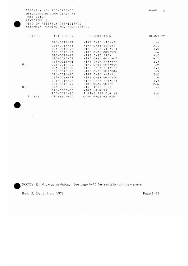
8/9/2019 KX 170A - Maintenance Manual Honeywell
http://slidepdf.com/reader/full/kx-170a-maintenance-manual-honeywell 299/586
ASSEMBLY ND. 200-0255-00
DESCRIPTION CONN CABLE SA
LJNIT KX175
REVISION 8
USED ON ASSEMBLY 069-1016-00
ASSEMBLY DRAWING NO. 300-0335-00
Rl
Rl
SYMBOL
PART NLJMBER
DESCRIPTIDN
025-0018-74 G/IRE CW26 VID/YEL
.6
025-0018-77 WIRF CW26 VIOLET
2.1
025-0018-79 WIRE CW26 VIIl/hJHT
1.9
025-0018-84 WIRE CW26 GRY/YFL
.6
025-0018-88
WIRE CW26 GRAY
4.0
025-0018-89 WIRE CW26 GRY/blHT 4.7
025-0018-91 MIRE Cb’26 WHT/BRN
1.7
025-0018-92 WIRE C’d26 WHT/RED
-9
025-0018-93 WIRE CW26 WHT/ORN
2.1
025-0018-95 MIRE CW26 WHT/GRN
1.5
025-0018-96
sx'IRE CW26 WHT/HL\J
2.0
025-0018-97
WIRE CW26 WHT/VID .H
025-0016-98 'JIRI CW26 WHT/GRY 1.7
025-0018-99
MIRE CW26 WHITE 2.6
026-0003-00 dIRE TC22 BLISS
.l
026-0005-00 WIRE 1.8 BIJSS
.l
150-0020-10 TUBING TEF CLR 18
2.0
P
171
030-2109-00
CDNN .MALE 42 PIN
1
PAGE 2
OlJANTI TY
NOTE: R indicates revision.
See page 6-70 for revision and new parts.
Rev, %, December, 1972
Page 6-69

8/9/2019 KX 170A - Maintenance Manual Honeywell
http://slidepdf.com/reader/full/kx-170a-maintenance-manual-honeywell 300/586
Parts List Revision R.ecord
Assembly No. 200-0255-00
Manual Revision 1
ACTION
SYMBOL
PART NUMBER
DESCRIPTION
QUANTITY
ADDED 025-0003-12
Wire 22 Red/Wht
.6
DELETE 025-0018-58
Wire CW26 Grn/Gry
1. 5
DELETE 025-0018-92
Wire CW26 Wht/Red
.9
DELETE 026-0003,-00
Wire TC22 Buss
. 1
ADDED 026-0013-00
Coax Cable RG178
.9
Page 6-70
a
ev. 2, December, 1972

8/9/2019 KX 170A - Maintenance Manual Honeywell
http://slidepdf.com/reader/full/kx-170a-maintenance-manual-honeywell 301/586
NAME
ASS’Y. NO.
1
ltase Converter
071-104 (
/O1
KING RADIO CORP. PARTS LISTING
f
QUANTITY
-I
-
PART NUMBER
DFSCRIPTION
-01
1
-
-
-00
-
X
2
1
4
1
0
AI;
. 11
.3
0
0
.l
.5
1
1
1
0
1
0
-
071-1041-00
071-1041-01
008-0022-00
008-0046-00
008-0063-00
008-0064-00
009-0003-03
010-0019-90
016-1004-00
025-0003-04
025-0003-05
025-0003-06
025-0003-08
026-0004-00
026-0005-00
047-1964-00
047-1965-00
057-1270-01
057-1366-01
073-0117-01
Casting, KA 38/KA39
076-0107-00
Grommet, Plastic
&v. 4, January, 1976
K-1651
KA 38 Single Reg
KA 39 Double Reg
Lug Solder
Lug Solder
Term. Wire
Lug, Solder
Term Strip
Term Standol
Thermal Compound
Wire #22AWG (Yel)
Wire #22AWG (Grn)
Wire #22AWG (Blu)
Wire #22AWG (Gry)
Wire, Cop #BOAWG
Wire, Buss #18AWG
Cover
Plate, Bottom
S/N Tag (KA 38)
Nameplate (KA 39)
SHTLOFLI
Page 6-71
X
1
1
AF
.l
.3
.2
.2
. 1
1.
1
1
0
1
1
1
- -

8/9/2019 KX 170A - Maintenance Manual Honeywell
http://slidepdf.com/reader/full/kx-170a-maintenance-manual-honeywell 302/586
NAME ‘.
Voltage Converter
.. (\ -
KING -RAOlO CORP. PARiS LISTIN‘G
: SYMBOL
PART .NlJM BER
. -
:.
c
DESCRIPTION
089,-2 140-00
: 089-2 147-22
089-5903-05
089-5963-08
089-5907-08
089-5907-12
089-5909-12
089-8005-34
089-8014-37
089-8017-37
089-8065-30
Nut, #4 ESNA
Nut, #6. ESNA
Ser. 4-40 x.5/16 PHP
Ser. 4-40 x.1/2 PHP
Ser. 6-32 x l/2”
Ser. 6-32 x 3/4 PHP
Ser. 8-32 x 3/4 PHP
Lock Washer
Lock Washer, Int. Tooth
Lock Washer, Int. Tooth
Washer, Flat
090-0162-00 Block Term.
091-0004-00
Mtg. Wsht,, Mica
091-0035-00
Wshr, Insul. Mica
09 l-0068 -04 Wshr, Shoulder
~150-0003-10
i50-0007-10
Tubing, Tef. #24
Tubing, Tef. #IS:
i :
QlOl
Q102
Q103
Q104 ;
Cl01
Cl02
007~0099-00 TSTR 2N4348
007-0159-00
TSTR 2N3441
007-0159-00
TSTR 2N3441
007-0038-00 TSTR 2N3053
105-003 l-50 Cap, My1 . d33pf *lo% 8oV
105-003 l-50 Cap My1 .033pf *lo% 80V
‘CR101
.007-5010-02
Dio. Zen 15V 1OW 2%
:R102
007-6021-00 Dio. TS-2 .,
CR193
,007;602 l-00
Dio. TS-2
zR104
007i5011-18 Dio. Zen 15V 1W 5%
RlOl
R102
:R103
R104:
132 -0 113 -00
132 -0 112 -00
132 -5004-00
132-0163-31
Res. 1R 40W 5%
Res. 150 ohms 5W 5%
Res. lK.0 2W 10%
Res. 6R 1OW 5%
.
I
,P?ge 6-72
K-1651'
_
4
1
8
4
3
1
2
.3
8
i
2
2
1
1
4
9
. 1
1
1
ii
0
1
0
1
1
0
0
1
1
E
-
i
6
1
'8
8
3
f
3
1
2
3
2
1
2
6
.
1.
:l
i2
-
1
2
1
2
1
.l
; 1
1
1
LNl
-
-02
I&
Rev. 4; January, 1976
.,

8/9/2019 KX 170A - Maintenance Manual Honeywell
http://slidepdf.com/reader/full/kx-170a-maintenance-manual-honeywell 303/586
PARTS LIST REVISION HISTORY
ENGR. APPROVAL
YAME
ASS’Y. NO.
Voltage Converter
071-1041-OO/Ol
\SS’Y. DWG.
UNIT
USED ON
300-0198-00 KA 38/KA 39
?EV CHANGE
SYMBOL
PART NUMBER
DESCRIPTION
1
2
3
4
5
6
7
8
9
10
11
12
13
14
15
16
17
Iev. 4, January, 1976 kHT-iv.OF 3 1
Page 6-73

8/9/2019 KX 170A - Maintenance Manual Honeywell
http://slidepdf.com/reader/full/kx-170a-maintenance-manual-honeywell 304/586
KING
KX 170A/KX 175
NAVIGATION RECEIVER/
COMMUNICATIONS TRANSCEIVER
0
0
Page 6-74
RlOl
CR103
Cl02
Cl01
CR102
CR101
R104
CR104
RI.03
R102
696-6105-00
FIGURE 6-12 KA 39 VOLTAGE CONVERTER
(Dwg. No. 696-6105-00)
Rev. 2, December, 1972

8/9/2019 KX 170A - Maintenance Manual Honeywell
http://slidepdf.com/reader/full/kx-170a-maintenance-manual-honeywell 305/586
KING
KX 170A/KX 175
NAVIGATION RECEIVER/
COMMUNICATIONS TRANSCEIVER
KX 170A Parts List (Electrical)
Description NAV/COMM Board SA
Unit KX 170A
SYMBOL PART NUMBER
DESCRIPTION
FL404
0 17 -0037 -00 Filter 15. 1875MHz
QUANTITY
1
NOTE :
The KX 175 Parts List also applies to the KX 170A except where differences
are noted on the schematics, Figures 5-50, 5-51, 5-52, 5-53, 5-54.
Rev, 2, December, 1972
Page 6-75

8/9/2019 KX 170A - Maintenance Manual Honeywell
http://slidepdf.com/reader/full/kx-170a-maintenance-manual-honeywell 306/586
w
KING,
KY 195
COMMUNICATIONSRANSCEIV
INSTALLATIONANUA
006-0062-0
REV. 1 JANUARY, 1976

8/9/2019 KX 170A - Maintenance Manual Honeywell
http://slidepdf.com/reader/full/kx-170a-maintenance-manual-honeywell 307/586
KlNG
KY 195
COMMUNICATIONS TRANSCEIVER
TABLEOFCONTENTS
SECTION
GENERALNFORMATION
Paragraph
Page
1.1 Introduction
1.2
Purpose of Equipment
1.3 Design Features
1.4 Power Requirements
1.5 Technical Characteristics
1.6
Units and Accessories Supplied
1.7
Accessories Required But Not Supplied
1.8 License Requirements
l-l
l-l
l-1
l-2
l-2
l-4
l-5
l-5
SECTIONI
INSTALLATION
2.1
General
2.2
Unpacking and Inspecting Equipment
2.3 KY 195 Installation
2.4 KA 39 Installation
2.5 Antenna Installation
2.6
Cabling
SECTIONll
OPERATION
3.1
General
3.2 KY 195 Comm Controls
3.3
Post-Installation Checkout
2-l
2-l
2-l
2-2
2-2
2-3
3-l
3-l
3-2
i

8/9/2019 KX 170A - Maintenance Manual Honeywell
http://slidepdf.com/reader/full/kx-170a-maintenance-manual-honeywell 308/586
KlNG
KY 195
COMMUNICATIONS TRANSCEIVER
HISTORYOF REVISIONS
Rev. 1, January, 1976
Page
Front Page
Table of Contents
2-9
Reason for Change
Added
Added
Interconnect Updated
ii

8/9/2019 KX 170A - Maintenance Manual Honeywell
http://slidepdf.com/reader/full/kx-170a-maintenance-manual-honeywell 309/586
KING
KY 195
COMMUNICATIONS TRANSCEIVER
SECTION
GENERALNFORMATION
1.1 INTRODUCTION
This manual contains information relative to the physical, mechanical and electrical
characteristics of the King Radio Corporation Silver Crown KY 195.
1.2 PURPOSEOF EQUIPMENT
The King KY 195 COMM combines in a single panel mounted unit a 360 channel VHF
COMM Transceiver with dual, independent, frequency selectors.
1.3 DESIGNFEATURES
A.
Controls
1.
2.
3.
4.
On-Off switch is independent of volume control settings allowing
the volume to remain at desired levels.
Dual control head with thumb switch selection of frequency select-
or A or frequency selector B.
Automatic squelch eliminates pilot responsibility for continuously
monitoring squelch adjustments.
Squelch threshold automatically
adjusts to open on readable signals.
Test position opens squelch
to test COMM receiver sensitivity and to listen to extremely weak
signals.
Frequency selector mechanism features human engineered concen-
tric knobs, airline type drum readout, and blue-white or red back
lighting.
B.
Electronics
1. Varactor diode tuned filters eliminates use of mechanical tuning
shafts and mechanisms.
2. Balanced mixers for superior intermodulation, cross modulation,
and L. 0. radiation performance.
3.
Transistorized transmitter provides 5 watts minimum output power
and long term reliability superior to tube designs.
Page l-l
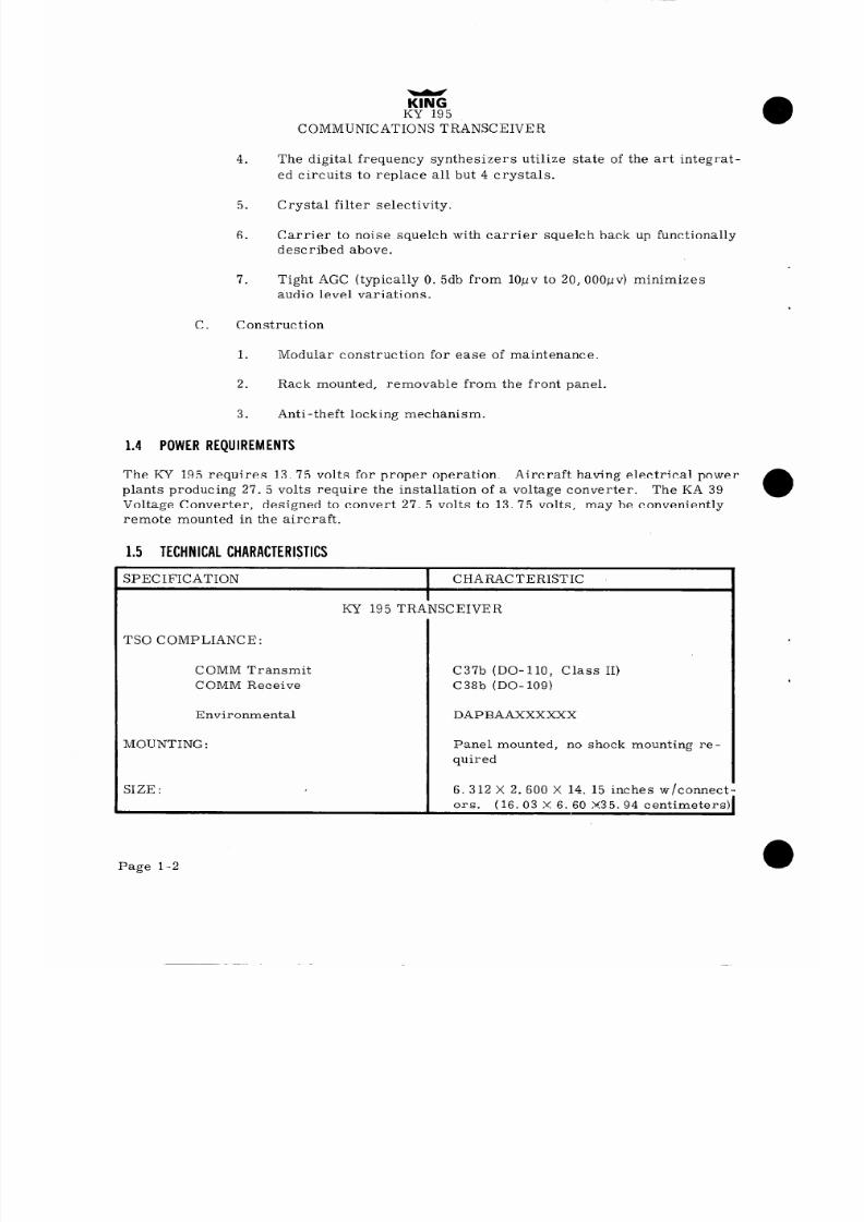
8/9/2019 KX 170A - Maintenance Manual Honeywell
http://slidepdf.com/reader/full/kx-170a-maintenance-manual-honeywell 310/586
KING
KY 195
COMMUNICATIONS TRANSCEIVER
4.
The digital frequency synthesizers utilize state of the art integrat-
ed circuits to replace all but 4 crystals.
5.
Crystal filter selectivity.
6. Carrier to noise squelch with carrier squelch back up functionally
described above.
7. Tight AGC (typically 0. 5db from 10~~ to 20, 000~~) minimizes
audio level variations.
C.
Construction
1.
Modular construction for ease of maintenance.
2. Rack mounted, removable from the front panel.
3. Anti-theft locking mechanism.
1.4 POWERREQUIREMENTS
The KY 195 requires 13. 75 volts for proper operation. Aircraft having electrical power
plants producing 27. 5 volts require the installation of a voltage converter.
The KA 39
Voltage Converter, designed to convert 27. 5 volts to 13. 75 volts, may be conveniently
remote mounted in the aircraft.
1.5 TECHNICAL HARACTERISTICS
SPECIFICATION CHARACTERISTIC
KY 195 TRANSCEIVER
TSO COMPLIANCE:
C OMM Transmit
COMM Receive
Environmental
MOUNTING :
C37b (DO-110, Class II)
C38b (DO- 109)
DAPBAAXXXXXX
Panel mounted, no shock mounting re-
quired
SIZE : 6. 312 X 2. 600 X 14. 15 inches w/connect
ors. (16. 03 X 6. 60 X35. 94 centimeters’
Page l-2
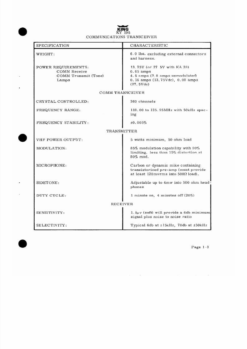
8/9/2019 KX 170A - Maintenance Manual Honeywell
http://slidepdf.com/reader/full/kx-170a-maintenance-manual-honeywell 311/586
KING
KY 195
COMMUNICATIONS TRANSCEIVER
SPECIFICATION
WEIGHT :
CHARACTERISTIC
6. 0 Ibs. excluding external connectors
and harness.
POWER REQUIREMENTS:
COMM Receive
C OMM Transmit (Tone)
Lamps
13. ‘75V (or 27. 5V with KA 39)
0.65 amps
4. 5 amps (2. 8 amps unmodulated)
0. 16 amps (13.75Vdc), 0.08 amps
(27. 5Vdc)
COMM TRANSCEIVER
CRYSTAL CONTROLLED:
FREQUENCY RANGE:
360 channels
118.00 to 135. 95MHz with 50kHz spac-
ing
FREQUENCY STABILITY :
*o. 005%
TRANSMITTER
VHF POWER OUTPUT:
MODULATION :
5 watts minimum, 50 ohm load
85% modulation capability with 90%
limiting, less than 150/Odistortion at
80% mod.
MICROPHONE :
Carbon or dynamic mike containing
transistorized pre-amp (must provide
at least 120mvrms into 50052 load).
SIDETONE :
Adjustable up to 4mw into 500 ohm heat
phones
DUTY CYCLE:
1 minute on, 4 minutes off (20%)
RECEIVER
SENSITIVITY: 1. 51.l~ (soft) will provide a 6db minimun
signal plus noise to noise ratio
SELECTIVITY:
Typical 6db at *15kHz, 70db at *SOkHz
Page l-3

8/9/2019 KX 170A - Maintenance Manual Honeywell
http://slidepdf.com/reader/full/kx-170a-maintenance-manual-honeywell 312/586
KING
KY 195
COMMUNICATIONS TRANSCEIVER
SPECIFICATION
SPURIOUS RESPONSES:
SQUELCH:
CHARACTERISTIC
Down at least 60db
Automatic squelch (carrier to noise)
with manual disable and carrier squelch
override.
AGC CHARACTERISTICS:
From 10~~ to 20,000~~ audio output will
not vary more than 3db.
AUDIO
AUXILARY AUDIO INPUTS :
Three (3) 500 ohms with 30db isolation
between any two.
FREQUENCY RESPONSES:
HEADPHONE OUTPUT :
SPEAKER OUTPUT:
Within 6db from 350Hz to 2500Hz.
50mw into 500 ohm
4. 5Vrms into auxilary input produces
5 watts audio output
KA 39 VOLTAGE CONVERTER
SIZE :
3. 500 X 2.000 X5. 500 inches
(8.889 X 5. 18 X 13. 87 centimeters)
WEIGHT :
POWER:
1. 1 lbs. excluding harness
A B
Input Volts 27. 5vdc 27. 5vdc
output Volts 13.75vdc
13. 75vdc
(nominal)
(nominal)
Output Current continuous 1. 5A 0.75A
Output Current 40% duty 5. OA
--------
1.6 UNITSAND ACCESSORIESUPPLIED
A.
King KY 195 COMM (069-1018-00)
B.
King KY 195 Installation Kit (050-1142-02 ) includes mating connectors,
radio rack, mounting hardware , red lamp filter, etc.
Page l-4

8/9/2019 KX 170A - Maintenance Manual Honeywell
http://slidepdf.com/reader/full/kx-170a-maintenance-manual-honeywell 313/586
KING
KY 195
COMMUNICATIONS TRANSCEIVER
1.7 ACCESSORIESEQUIRED UT NOT SUPPLIED
A. Communication antenna and cables
B.
Headphones and speaker:
1.
Headphones :
Low impedance types, 300 to 1,000 ohms.
2.
Speaker : Voice coil impedance 3 to 6 ohms nominal.
C. KA 39 Voltage Converter,
27. 5V to 13. 75V (required in 27.
5V install-
ation only).
D.
Microphone :
Low impedance carbon, or dynamic with transistor pre-
amp, such as King KA 14.
1.8 LICENSEREQUIREMENTS
The Federal Communications Commission requires that the operator of the transmitter
in this equipment hold a Restricted Radio Telephone Operator Permit, or higher c lass
license.
A permit may be obtained by an U. S. citizen from the nearest field office of
the FCC; no examination is required.
This equipment has been type accepted by the FCC and entered on their list of type
accepted equipments as King KY 195 and must be identified as King KY 195.
-CAUTlON-
The VHF transmitter in this equipment
is guaranteed to meet Federal Communications
Commiss ion approval only when King crystals
are used.
Use of other than King crystals is considered
an unauthorized modification.
Page l-5
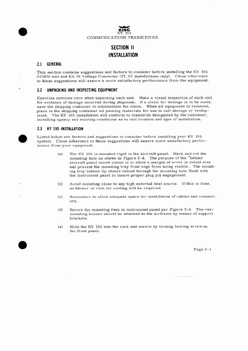
8/9/2019 KX 170A - Maintenance Manual Honeywell
http://slidepdf.com/reader/full/kx-170a-maintenance-manual-honeywell 314/586
KING
KY 195
COMMUNICATIONS TRANSCEIVER
SECTIONI
INSTALLATION
2.1 GENERAL
This section contains suggestions and factors to consider before installing the KY 195
COMM unit and KA 39 Voltage Converter (27. 5V installations only).
Close adherence
to these suggestions will assure a more satisfactory performance from the equipment.
2.2 UNPACKINGAND INSPECTING QUIPMENT
Exercise extreme care when unpacking each unit.
Make a visual inspection of each unit
for evidence of damage incurred during shipment.
If a claim for damage is to be made,
save the shipping container to substantiate the claim. When all equipment is removed,
place in the shipping container all packing materials for use in unit storage or reship-
ment.
The KY 195 installation will conform to standards designated by the customer,
installing agency and existing conditions as to unit location and type of installation.
2.3 KY 195 INSTALLATION
Listed below are factors and suggestions to consider before installing your KY 195
system.
Close adherence to these suggestions will assure more satisfactory perfor-
mance from your equipment.
(a)
(b)
(c)
(4
(4
The KY 195 is mounted rigid in the aircraft panel.
Mark and cut the
mounting hole as shown in Figure 2-4. The purpose of the “behind
aircraft panel mount cutout is to allow a margin of error in cutout size
and prevent the mounting tray front edge from being visible.
The mount-
ing tray bottom lip should extend through the mounting hole flush with
the instrument panel to insure proper plug pin engagement.
Avoid mounting close to any high external heat source.
If this is done,
no blower or ram air cooling will be required.
Remember to allow adequate space for installation of cables and connect-
ors.
Secure the mounting rack to instrument panel per Figure 2-4. The rear
mounting bosses should be attached to the airframe by means of support
brackets.
Slide the KY 195 into the rack and secure by turning locking screwon
the front panel.
Page 2-1

8/9/2019 KX 170A - Maintenance Manual Honeywell
http://slidepdf.com/reader/full/kx-170a-maintenance-manual-honeywell 315/586
COMMUNICATIONS TRANSCEIVER
-CAUTION -
Do not force locking tab screw.
(f) Each KY 195 installation kit contains a locking bar (KPN 047-1720-00),
bracket (KPN 047-1721-00) and two rivets (KPN 092-5021-00).
These
may be installed at customer’s option to provide a means of locking
the radio to the instrument panel with a padlock located on the lower
rear corner of the mounting tray.
Installation consists of riveting the bracket to the mounting tray as
shown in Figure 2-4.
After the radio installation is complete, the
locking bar may be inserted and a small padlock affixed to deter theft.
(g) The installing agency will supply and fabricate all external cables.
The plugs required are supplied by King Radio.
2.4 KA 39 INSTALLATION
(For use in 27. 5 volt installations only)
(a) Select the KA 39 location considering good thermal conductivity to
the airframe, convenient cable routing, proximity to the KY 195 and
separation from other heat sources.
(b) Refer to Figure 2-3 for the KA 39 mounting dimensions.
(c) Secure the KA 39 firmly in place.
(d) The installing agency will supply and fabricate external cables.
2.5 ANTENNA NSTALLATION
(a) A conventional 50 ohm vertically polarized COMM antenna is required
with the KY 195. Vertical bent whip antennas are not recommended.
Wideband COMM antennas (KA 3 1 and KA 3 1A) provide efficient
operation over the COMM band. Antennas should be installed per
manufacturers recommendations.
Additional recommendations are
as follow:
1. Mount antenna on flat metal surface or install a ground plane at
least 18 inches square.
2. The antenna should be well r.emoved from any projections and
the engine(s) and propeller.
3. The COMM Antenna should be well separated from any NAV
Antenna to minimize COMM interference to NAV while transmit-
ting.
Page 2-2

8/9/2019 KX 170A - Maintenance Manual Honeywell
http://slidepdf.com/reader/full/kx-170a-maintenance-manual-honeywell 316/586
Y
NI 5
COMMUNICATIONS TRANSCEIVER
(b)
Refer to Figure 2-2 for the COMM antenna cable connector assembly.
Solder tack the snap on shield to the connector base at two points to
insure that a good electrical ground is made.
2.6 CABLING
(4
The length and routing of the external cables must be carefully studied
and planned prior to installation. Avoid sharp bends and placing cables
too near the aircraft control cables.
(b)
Fabricate the external cables in accordance with the installation draw-
ing that fulfills the system requirement.
-NOTE-
Use good quality stranded wire that
will not support a flame and with at
least 600 volt insulation. It is re-
commended that the mike audio line
be in a shielded -twisted pair.
(c)
Since other radio equipment will possibly utilize the same speaker cir-
cuits for muting, speaker selection and microphone switching must be
devised by the installing agency. The KY 195 does not shunt the speaker
line of other equipment when the off-on-test switch is turned “off”.
PI71
CONNECTOR VIEWED
KPN030-2101-04
FROM CAKE END
696-6002-00 (R-01
FIGURE 2-l KY 195 CONNECTOR PIN LOCATIONS
Page 2-3

8/9/2019 KX 170A - Maintenance Manual Honeywell
http://slidepdf.com/reader/full/kx-170a-maintenance-manual-honeywell 317/586
KING
KY 195
COMMUNICATIONS TRANSCEIVER
Trim coax cable outer insulation as shown.
Fold braid back over outer cover of coax.
Do not cross strands.
Solder center conductor to center pin of
conductor.
Make sure front end of braid
(Point of fold) is even with bottom of con-
nector. (Shown by arrows)
Slide connector cap, with clearance hole in
position to clear d ielectric, on to connector
until it snaps in place.
Push braid forward and flatten against con-
nector cap and solder.
Solder tat connector cap.to connector in at
least two places to insure good electrical
contact.
696-6003-00
FIGURE 2-2 ANTENNA CABLE ASSEMBLY
Page 2-4

8/9/2019 KX 170A - Maintenance Manual Honeywell
http://slidepdf.com/reader/full/kx-170a-maintenance-manual-honeywell 318/586
zis
KY 195
COMMUNICATIONS TRANSCEIVER
NOTES :
I, ALL DIMENSIONS IN PARENTHESIS ARE IN CENTIMETERS.
ZWEIGHT: I.1 Ibo
3 TERMINALS WILL TAKE 16 TO22 AWG WIRE.
4.TERMINALS ARE =5-40X 114 BD. HD. SCREWS.
USE% PAN. HD. SCREWS
TO HEATER DUCTOROTHE RSOURCESOFHEAT
155-5076-00 (R- )
FIGURE 2-3 KA 39
VOLTAGE CONVERTER OUTLINE AND MOUNTING DRAWING
Page 2-5
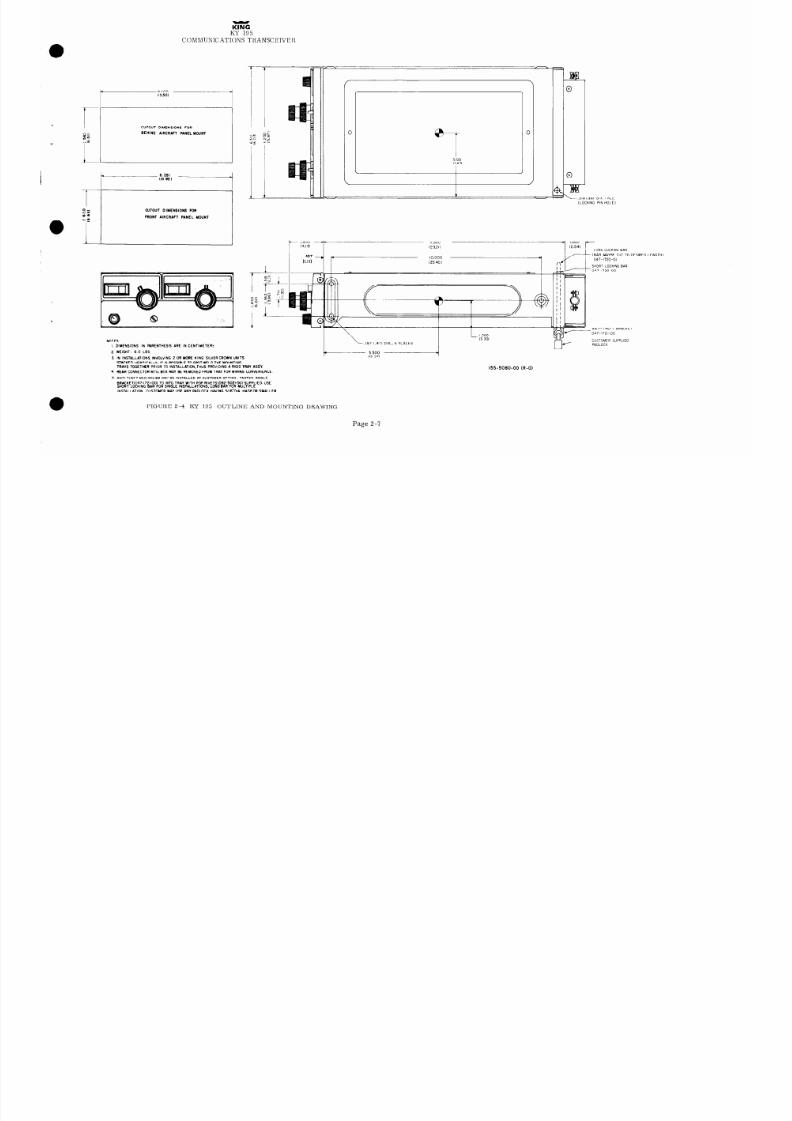
8/9/2019 KX 170A - Maintenance Manual Honeywell
http://slidepdf.com/reader/full/kx-170a-maintenance-manual-honeywell 319/586
KING
KY 195
COMMUNICATIONS TRANSCEIVER
l-r
-
6.100
(15.50)
CUTOUT DIMENSIONS FOR
BEHIND AIR~RM PANEL YOUHT
0
@
7
0
3 IO0
I7 87)
\
/
6.261
(IS 95)
-2 l6 t55 ) D IA. I PLC.
(LOCKING PIN HOLE)
CUTOUT DIMENSIONS FOR
FRONT AIRCRAFT PANEL MOUNT
LONG LOCKING EAR
-(BAR MAYBE CUT TO DESIRED LENGTH)
047-1720-01
SHORT LOCKING BAR
047-1720-00
ANTI-THEFT BRACKET
047-1721-00
CUSTOMER SUPPLIED
y PADLOCK
I k
.I87 c.47) DIA.. 6 PLACES
OTES.
I. DIMENSIONS IN WRENTHESIS ARE IN CENTIMETER\
2. WEIGHT: 6.0 LES
3 IN INSTALLATIONS INVOLVING 2 OR YORE KING SILVER CROWN UNITS
STACKED VERTICALLY. IT IS POSSIBLE TO SPOT WELD THE MOUNTNG
TRAYS TOGETHER PRIOR TO INSTALLATION.TH US PROVIDING A RIGID TRAY ASSY
4. REAR CONNECTOR MTG BOX MAY BE REMOVED FROM TRAY FOR WIRING CONVENIENCE
L
5. ANTI THEFT MECHANSM MAY BE INSTALLED AT CUSTOMER OPTION. FASTEN ANGLE
BRACKETl047-1721-00) TO MTG TRAY WITH POP RlVETS(092-502kC’J) SUPPLIED. USE
SHORT LOCKING BAR FOR SINGLE INSTALLATIONS, LONGBAR FOR MULTIPLE
INSTALLATION. CUSTOMER MAY USE ANY PADLOCK HAVNG 3/16’D IA . WASPOR SMALLER.
155-5080-00 (R-0)
FIGURE 2-4 KY 195 OUTLINE AND MOUNTING DRAWING
Page 2-7
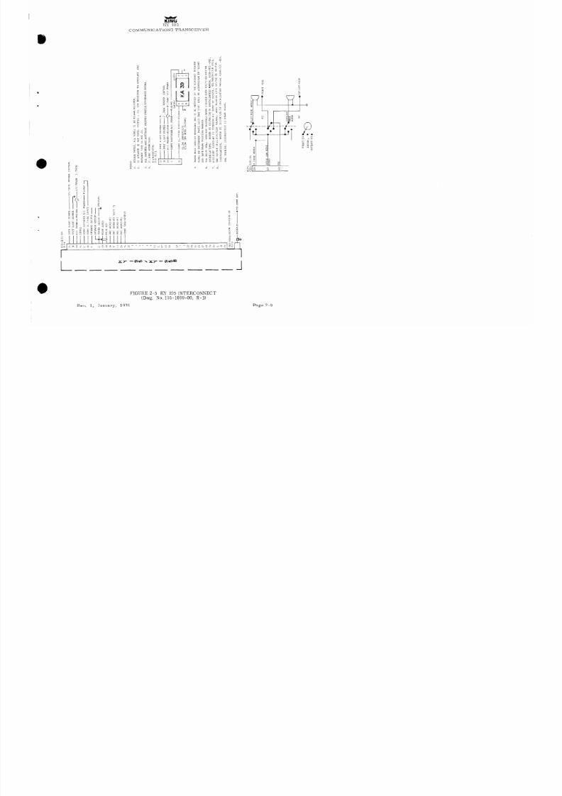
8/9/2019 KX 170A - Maintenance Manual Honeywell
http://slidepdf.com/reader/full/kx-170a-maintenance-manual-honeywell 320/586
KING
KY 195
COMMUNICATIONS TRANSCEIVER
-4----gi-t- j--- Q
FIGURE 2-5 KY 195 INTERCONNECT
(Dwg. No. 155-1099-00, R-3)
Rev. 1, January, 1976
Page 2-9

8/9/2019 KX 170A - Maintenance Manual Honeywell
http://slidepdf.com/reader/full/kx-170a-maintenance-manual-honeywell 321/586
i?iK
KY 195
COMMUNICATIONS TRANSCEIVER
SECTIONII
OPERATION
3.1 GENERAL
All controls required to operate the KY 195 are located on the unit front panel.
3.2 KY 195 COMM CONTROLS
3.2. 1
COMM ON-OFF TEST CONTROL
The ON-OFF-TEST control is located directly above the COMM A channel selector.
Power is supplied to the COMM when this control is either in the ON or TEST position.
The TEST position is used to defeat the COMM automatic squelch for both test purposes
and listening to extremely weak signals.
3.2.2
COMM VOLUME CONTROL
The Volume (VOL) control, located on the lower left s ide of the KY 195 is used to adjust
the transceiver audio volume. The KY 195 system power ON/OFF switch is independent
of this control, allowing the COMM volume to remain at a desired preset level.
3.2. 3
COMM A FREQUENCY SELECTOR
The twoconcentric knobs under the COMM A frequency window are used to dial COMM
A frequencies. The larger knob selects MHz and the smaller knob selects KHz. The
transceiver is inoperable in the two unused MHz positions between 118MHz and 135MHz.
Clockwise rotation selects higher frequencies. The dial mechanism has no stops, per-
mitting continuous rotation.
3.2.4
COMM B FREQUENCY SELECTOR
The two concentric knobs under the COMM B frequency window are used to dial COMM
B frequent ies. The larger knob selects MHz and the smaller knob selects KHz.
The
transceiver is inoperable in the two unused MHz potitions between 118MHz and 135MHz.
Clockwise rotation selects higher frequencies.
The dial mechanism has no stops, per-
mitting continuous rotation.
3.2. 5 A-B SELECTOR CONTROL
The A-B leverswitch is used to select control head A or control head B.
Page 3-l

8/9/2019 KX 170A - Maintenance Manual Honeywell
http://slidepdf.com/reader/full/kx-170a-maintenance-manual-honeywell 322/586
a5
COMMUNICATIONS TRANSCEIVER
COMM A FREQUENCY READOUT
MHz FREQUENCY SELECTOR
I’ \
KHz FREQUENCY SELECTOR
I
COMM B
FREQUENCY
READOUT
KHz FREQUENCY SELECTOR
\
MHz FREQUENCY SELECTOR
696-6106-00
FIGURE 3- 1 KY 195 CONTROL FUNCTIONS
3.3 POST-INSTALLATIONHECKOUT
1
An operational performance flight test is recommended after the installation is corn-
pleted to insure satisfactory performance of the equipment in its normal environment.
To check the communications transceiver,
maintain an appropriate altitude and contact
a ground station facility at a range of at least fifty nautical miles.
Contact a ground
station close in.
Place the squelch knob in the test position and listen for any unusual
electrical noise which would reduce the COMM receiver sensitivity by increasing the
squelch threshold.
If possible, verify the communications capability on both the HIGH
and LOW ends of the VHF COMM band.
Page 3-2

8/9/2019 KX 170A - Maintenance Manual Honeywell
http://slidepdf.com/reader/full/kx-170a-maintenance-manual-honeywell 323/586
MAINTENANCE/OVERHAUL
MANUAL
KY 195
COMMUNICATIONS
TRANSCEIVER
KING RADIO CORPORATION,
400 NORTH ROGERS ROAD
OLATHE, KANSAS, U.S.A.

8/9/2019 KX 170A - Maintenance Manual Honeywell
http://slidepdf.com/reader/full/kx-170a-maintenance-manual-honeywell 324/586
KING
KY 195
COMMUNICATIONS TRANSCEIVER
TABLE FCONTENTS
Paragraph
SECTIONV THEORY FOPERATIONNDMAINTENANCE
4. 1 General
4. 2 Dual Control Head
4. 3 Dual Control Head-Detailed Description
4.4 Troubleshooting The Dual Control Head.
Item
1. KY 195
5-l
2.
Front Plate Sub-Assembly
5-l
3. Switch Head Sub-Assembly 5-2
4.
Switching Matrix Assembly
5-10
5.
COMM SMO Board Sub-Assembly
5-14
6. COMM SMO Sub-Assembly
5-14
7.
Receiver Board Sub-Assembly
5-14
8. Transmitter Assembly
5-16
9. Rear Plate Assembly
5- 16
10.
Audio Drive Board
5-16
11. Rear Divider Sub-Assembly
5-16
12.
COMM Cable Sub-Assembly
5-16
Figure
2-l KY195 Connector Pin Locations
2-3
2-2 Antenna Cable Assembly
2-4
2-3 KA 39 Voltage Converter Outline and Mounting Drawing
2-5
SECTION ILLUSTRATEDARTS IST
LISTOF LLUSTRATIONS
4-l
4-l
4-l
4-2
Page
Page
i

8/9/2019 KX 170A - Maintenance Manual Honeywell
http://slidepdf.com/reader/full/kx-170a-maintenance-manual-honeywell 325/586
KING
KY 195
COMMUNICATIONS TRANSCEIVER
TABLE FCONTENTS
Figure
2-4 KY 195 Outline and Mounting Drawing
2-7
2-5
KY 195 Interconnect
2-9
3-l KY 195 Control Functions
3-2
S-1A Switching Head Sub -Assembly
5-5
S-1B
Switching Head Sub-Assembly
5-7
5-2
Switching Matrix AssembJy
5-11
5-3
Receiver Board Sub-Assembly
5-15
Page
ii

8/9/2019 KX 170A - Maintenance Manual Honeywell
http://slidepdf.com/reader/full/kx-170a-maintenance-manual-honeywell 326/586
COMMUNICATIONS TRANSCEIVER
SECTIONV
THEORY FOPERATIONNDMAINTENANCE
4.1 GENERAL
KY 195 unit incorporates a 360 channel communications transceiver, a 5 watt audio
system, and dual control heads.
The transceiver and audio systems are identical to
the respective portions of the KX 175.
For theory and maintenance procedures on the
COMM transceiver or audio system, refer to the KX 175 text. Theory and maintenance
of the dual control head mechanism appear in this section.
4.2 DUAL CONTROL EAD
Wafer switches in the KY 195 are identical to the COMM wafer switches used in the
l-2; 175. Lever switch “A-B” applies either
“A” or “B” channeling information to the
SMC) and “A” or “B” tuning voltage to the varactor tuned filters in the COMM receiver
preselector.
4.3 DUALCONTROL EAD-DETAILEDESCRIPTION
Refer to Figure 5-55 in the KX 170A/ KX 175 Maintenance Manual for the KY 195 Switch-
ing Assembly Diagram.
4. 3. 1 Control Head Selector ln “A” Position
The DPST switch (Sill) contacts are open and the “B” tuning voltage (red-blue wire)
from switch wafer S106 is disconnected from the COMM tuning voltage buss.
Addition-
ally, the common wire to the
“B” switch wafers (red-gray wire) assumes a voltage o f
approximately 8 volts, back biasing the isolation diodes associated with the “B” wafer
switches which effectively disconnects the
“B” switching circuitry from the COMM SMO.
‘rransistors Q201-Q204 are saturated.
Q204 shorts the common wire of the “A” switch
wafers (brown-gray wire) to ground, activating the “A”
wafer switch functions. Q203
connects the negative side of the
“A” tuning voltage divider on switch wafer, S102, to
ground while Q201 connects the positive side to +8. 5VDC providing a current path
through the tuning voltage divider.
The “A” tuning voltage from switch wafer S102 is
connected directly to the COMM tuning voltage buss (red-blue wire) providing “A”
tuning voltage to the COMM receiver preselector.
4. 3. 2 Control Head Selector In “B” Position
The DPST switch (Sill) contacts are closed, connecting (a) the COMM tuning voltage
from switch wafer S106 to the tuning voltage buss (red-blue wire) and (b) the common
wire of the “13” switch wafers (red-gray wire) to ground.
With the common wire on
ground, the “B” channeling wafers are activated and transistors QZOl-Q204 are off.
April, 197 I
Page 4-l

8/9/2019 KX 170A - Maintenance Manual Honeywell
http://slidepdf.com/reader/full/kx-170a-maintenance-manual-honeywell 327/586
KING
KY 195
COMMUNICATIONS TRANSCEIVER
With Q203 and Q201 off, no current flows through the “A” tuning voltage divider on switch
wafer S102, isolating it from the COMM tuning voltage buss (red-blue wire). With Q204
off, the “A” wafers and associated isolation diodes represent an open circuit to the
COMM SMO frequency selection circuitry.
4.4 TROUBLESHOOTINGHEDUALCONTROLEAD
Refer to Figure 5-55 in the Kx 17OA/KX 175 Maintenance Manual for the KY 195 switching
matrix voltage measurements. See the KX 175 Manual for channeling malfunctions, refer
to Table 4-4 “COMM Programmable Counter Coding” and for COMM receiver preselector
tuning voltage versus channel frequency see Table 5-4 “COMM Channel-Receive SMO
Frequency-Tuning Voltage. ”
Page 4-2
April, 197 1

8/9/2019 KX 170A - Maintenance Manual Honeywell
http://slidepdf.com/reader/full/kx-170a-maintenance-manual-honeywell 328/586
is5
KY 195
C OMMUNIC ATIONS
T RANSC EW E R
1.
KY 195 - See Page 6-l and 6-2 in KX 17OAIKX 175 Maintenance Manual.
2.
Front Plate Sub-Assembly - See Page 6-3 thru 6-5 in KX 170A/KX 175
Maintenance Manual.
April, 197 1
Page 5-l

8/9/2019 KX 170A - Maintenance Manual Honeywell
http://slidepdf.com/reader/full/kx-170a-maintenance-manual-honeywell 329/586
NO. 200-0253-01
ON SWIT CHING HEAD
KY 195
ON ASSEMBLY 069-1018-00
DRAWING NO. 300-0429-00/14
SYMBOL PART NUMBER
R2 029-0095-00
047-16.75-01
047-1714-00
047-2115-00
047-2208-02
R2 076-0284-02
076-0299-00
076-0298-00
076-0298-01
R2 076-0472-01
R2 076-0473-00
088-0136-00
R2 088-0213-10
R2 088-0213-12
089-2005-37
089-2076-30
089-2140-00
089-5381-21
089-5857-04
R2 089-5857-06
089-5903-04
089-5903-06
R2 089-6289-03
089-8003-34
089-8023-30
089-8025-30
R2 089-8079-10
090-0140-02
090-0160-00
091-0015-00
091-0015-11
091-0018-05
091-0068-04
097-0056-33
l03
Cl04
113-5151-01
PAGE 1
DESCRIPI’ION
QUANTITY
GEAR, FACE
SUPPORT, DIAL
BRACKET, SWITCH
BRACKET, SWITCH
PLATE, DIAL MOUNTING
SHAFT, COUNTER WHEEL
COLLAR
SPACER, . 187 Lg.
SPACER, . 218 Lg.
3/8” SWITCH SHAFT 1. 015
l/4” SWITCH SHAFT
FILTER, BLUE LAMP
COUNTER WHEELS, KHz
COUNTER WHEELS, COMM, MHz
NUT STANDARD HEX
NUT, 4-40
NUT ESNA
SCREW MACH. 2-56 X 1 5/16
SCREW SET 4-40 X l/8 BRISTOL
#4-40 X 3/16 SET SCREW
SCREW, 4-40 X l/4 PHP
SCREW, 4-40 X 318 PHP
#4-40 X 3/16 HEX HD SCREW
LOCKWASHER #4 SPLIT RING
FLAT WASHER
WASHER #4
WASHER, . 25 I.D.
SOCKET, LAMP
SOCKET, LAMP
GROMMET
GROMMET
WASHER
WASHER, SHOULDER
CAPACITOR, ALUM.
lOOmf, 16V
CAPACITOR, D/C
150pf, lo%, X5F
Note: R indicates Revision.
See Page 5-4A for Revision and New Parts.
2
1
1
1
1
2
2
4
12
2
2
2
2
2
4
1
6
4
4
4
2
1
6
1
4
1
2
1
1
3
1
2
1
1
1
Page 5-2
Rev. 2, December, 1972

8/9/2019 KX 170A - Maintenance Manual Honeywell
http://slidepdf.com/reader/full/kx-170a-maintenance-manual-honeywell 330/586
ASSEMBLY NO. 200-0253-01
DESCRIPTION SWITCHING HEAD
UNIT KY 195
REVISION 8
USED ON ASSEMBLY 069-1018-00
ASSEMBLY DRAWING NO.
300-0429-OO/ 14
SYMBOL
Cl05
CR101
007-6033-00
CR102
007-6033-00
CR103
007-5016-00
DSlOl 037-0007-10
DS102
037-0007-10
QlO2 007-0184-01
Q104
007-0078-00
Q105
007-0078-02
R4 Rlll
136-2941-22
Rl12
136-4020-22
R113
136-4530-22
R114 136-5110-22
R4 R115 136-5620-22
R116 136-6340-22
R117
136-6980-22
R118
136-7870-22
R119 136-8660-22
R120
136-6340-22
R125 130-0680-33
R129
130-0102-25
R130 130-0152-23
R131 130-0471-23
R4 R132
133-5620-22
R133
130-0102-25
R2 R135
136-2941-22
R2 R136
136-4020-22
R2 R137
136-4530-22
R2 R138
136-5110-22
R2 R139
136-5620-22
R2 R140
136-6340-22
R2 R141
136-6980-22
R2 R142
136-7870-22
R2 R143
136-8660-22
R2 R144
136-6340-22
SlOl
031-0104-00
PART NUMBER
DESCRIPTION
113-5151-01
CAPACITOR, D/C
150pf, lo%, X5F
DIODE, lN270
DIODE, IN270
DIODE, ZENER 5. lV, 50/o, 1W
LAMP, T 1 3/4. 14V WHITE
LAMP, T 1 3/4, 14V WHITE
TRkNSISTOR, TA755 7
TRANSISTOR, 2N34 15
TRANSISTOR, 2N3416
RESISTOR, 2. 94K. 170, l/SW
RESISTOR, 402a2, 170, 1/8W
RESISTOR, 453fZ2, 170, 1/8W
RESISTOR, 511Q2, 170, 1/8W
RESISTOR, 562fi2, 170, 1/8W
RESISTOR, 63452, l%, 1/8W
RESISTOR, 698fi, 170, I/ 8W
RESISTOR, 7870, 170, 1/8W
RESISTOR, SSS?, l%, l/ 8W
RESISTOR, 634a, l%, l/SW
RESISTOR, 68R, 570, 1/2W
RESISTOR, lOOOR, lo%, 1/4W
RESISTOR, 1. 5KR, 570, 1/4W
RESISTOR, 47Oa, 5%, 1/4W
POTENTIOMETER, 1KR
RESISTOR, lOOOR, lo%, 1/4W
RESISTOR, 2. 94K, 1%, 1/8W
RESISTOR, 4020, 170, l/ 8W
RESISTOR, 4530,
170,
1/8W
RESISTOR, 511n, 170, 1/8W
RESISTOR, 5629, 170, l/ 8W
RESISTOR, 634n, 170, 1/8W
RESISTOR, 6980, 170, l/ 8W
RESISTOR, 787n, 170, 1/8W
RESISTOR, 8660, l%, l/SW
RESISTOR, 6340, 170, l/ 8W
SWITCH, WAFER
Note: R indicates Revision.
See Page 5-4A for Revision and New Parts.
PAGE 2
QUANT IT Y
1
1
1
1
1
1
1
1
1
1
1
1
1
1
1
1
1
1
1
1
1
1
1
1
1
1
1
1
1
1
1
1
1
1
1
1
_ Rev. 4, January, 1976
Page 5-3

8/9/2019 KX 170A - Maintenance Manual Honeywell
http://slidepdf.com/reader/full/kx-170a-maintenance-manual-honeywell 331/586
ASSEMBLY NO. 200-0253-01
DESCRIPTION SWmCHING HEAD
UNIT KY 195
REVISION 8
USED ON ASSEMBLY 069-1018-00
ASSEMBLY DRAWING NO. 300-0429-00/14
SYMBOL PART NUMBER
R4 S102
s103
s104
s105
R2 S106
s107
S108
031-0107-00
SWITCH, WAFER
031-0106-00
SWITCH, WAFER
031-0105-00
SWITCH, WAFER
031-0104-00
SWITCH, WAFER
031-0107-00
SWITCH, WAFER
031-0106-00
SWITCH, WAFER
031-0105-00
SWmCH, WAFER
R4 008-0001-01
R4
008-0005-03
R4
016-1004-00
R4
016-1008-04
R4
016-1016-00
R4
025-0018-00
R4
025-0018-11
R4 025-0018-26
R4
025-0018-88
R4
026-0001-00
R4
037-0007-10
R4
150-0003-10
R4
150-0020-10
DESCRIPTION
SOLDER LUG 2
SOLDER LUG
7
THERMAL COMPOUND AR
CLYPTAL. PURPLE
AR
LUBRICANT AR
WIRE #26 BLK
.4
WIRE #26 BRN
.6
WIRE #26 RED/BLU
.8
WIRE #26 GRY
.7
BUSS WIRE #26
.4
LAMP T 1 3/4 14V WHT. 2
TEFLON TUBING #24
.5
SHRINK TUBING .6
PAGE 3
QUANTITY
Note: R indicates Revision.
See Page 5-4A for Revision and New Parts.
Page 5-4
Rev. 4, January, 1976

8/9/2019 KX 170A - Maintenance Manual Honeywell
http://slidepdf.com/reader/full/kx-170a-maintenance-manual-honeywell 332/586
Parts List Revision Record
Assembly No: 200 -02 53 -0 1
Manual Revision 2
ACTION SY MBGL PART NUMBER DESCRIPTION QUANTITY
ADDED
DELETED
DELETED
DELETED
DELETED
DELETED
DELETED
DELETED
DELETED
DELETED
DELETED
DELETED
DELETED
DELETED
DELETED
DELETED
DELETED
DELETED
CHANGE
CHANGE
CHANGE
ADD
ADD
R136
R137
R138
R139
R140
R144
R141
R142
R143
S106
R135
From
To
150-0005-10
089-8079-10
029-0095-00
076-0284-02
136-4020-22
136 -4530 -22
136-5110-22
136-5620-22
136-6340 -22
136-6340-22
136-6980-22
136-,787O -22
136-8660-22
088-0213-01
076-0472-01
076-0473-00
089-5857-06
089-6289-03
200-0575-04
136-2941-22
088-0213-02
200 -0 578 -00
200 -0 578 -02
200 -0 578 -0 1
#20 Teflon Tubing
.3
Washer, .25 I. D.
2
Gear Face
2
Shaft, Counter Wheel
2
Res. 402 1% EW
1
Res. 453 1% EW
1
Res. 511 1% EW
1
Res. 562 1% EW
1
Res. 634 1% EW
1
Res. 634 1% EW
1
Res. 698 1% EW
1
Res. 787 1% EW
1
Res. 866 1% EW
1
Counter Wheels, KHz
2
3 /8” Switch Shaft 1.015
2
l/4” Switch Shaft
2
#4-40X3 / 16 Set Screw
4
#4-40X3 / 16 Hex HD SCR 6
Switch Ass’y COMM
1
Res. 2.94K 1% QW
1
Counter Wheel COMM MHz 2
Wheel Ass’y COMM MHz 2
Gear Ass’y COMM
2
Wheel Ass’y COMM KHz 2
Assembly No: 200-0253-01
(B/M RL Rev #8)
Manual Revision 4
ADDED
008-0001-01
SOLDER L,UG 2
ADDED
008-0005-03
SOI,DER LUG
7
ADDED
016-1004-00
THERMAL COMPOUND AR
ADDED
016-1008-04
GLYPTAL. PURPLE
AR
ADDED
016-1016-00
LUBRICANT AR
ADDED
025-0018-00
WIRE #26 BLK .4
ADDED
025-0018-11
WIRE #26 BRN
6
ADDED
025-0018-26
WIRE #26 RED/BLU 8
ADDED
025-0018-88
WIRE #26 GRY 7
ADDED 026-0001-00 BUSS WIRE #26 4
x.
ADDED
037-0007-10
LAMP, T 1 3/4 14V WHT 2
ADDED
150-0003-10
TEFLON TUBING #24 5
ADDED
150-0020-10
SHRINK TUBING
.6
Rev. 4 <January 1976
Page 5-4A

8/9/2019 KX 170A - Maintenance Manual Honeywell
http://slidepdf.com/reader/full/kx-170a-maintenance-manual-honeywell 333/586
Parts List Revision Rec,ot-d
Assembly No: 200-0253-01 (B/M RL, Rev. #8)
Manual Revision 4 (C’ont’d)
ACTION SYMBOL PART NUMBER DESCRIPTION QUANTITY
CHANGE Rlll 136-2941-22
RES 2 94K 1% QW
1
CHANGE R132 133-0016-02
POT. IK
1
DEI,ETED R115 136-5620-22
RES 562 1% EW
1
CHANGE s102 200-0575-04
SWITCH ASS’Y. COMM
1
Page 5-4B
Rev. 4 January, 1976

8/9/2019 KX 170A - Maintenance Manual Honeywell
http://slidepdf.com/reader/full/kx-170a-maintenance-manual-honeywell 334/586
KlNG
KY 195
COMMUNICATIONS TRANSCEIVER
047-2115 -09 -,,I
FIGURE 5-1A SWITCHING HEAD SUB-ASSEMBLY
(Dwg. No. 300-0429-00 Rev. 2)
-0\05-00
(5 134)
Rev. 2 December, 1972
Page 5-5

8/9/2019 KX 170A - Maintenance Manual Honeywell
http://slidepdf.com/reader/full/kx-170a-maintenance-manual-honeywell 335/586
KING
KY 195
COMMUNICATIONS TRANSCEIVER
I. [1 NEARSIDE TERM.
2. 3 FARSIDE TERM.
3.
SWITCHES READ FROM LEFT SIDE OF UNIT
200-0575-04
(WHT/VIO) PI261
r
I27 (WHT)
rPl28 (WHTIELU)
(wHT/GRY) p125-
\
PI29 (RED/GRYl
RI43
-PI32 (RED/ELU)
PI33 (ORNIGRY)
L
iPl4l N. C
031~gvg-00
REF. DSIOI
PI24 (SlO4)
WHT
.
DSIOI
PI 17 (5103)
2 ;*a
Y
DSl02
PI I7 (5103)
610
ELK
WHT
025-00~6~9~
PI I I (5103)
PI35(SlO71
Y
GRY
Pll6(SlO3)
Pl4o(slo7)
6’-$
Y
. -26
Pl32(SlO6
P502
6’6”
&LU TD FRONT PLATE (x)0-0431-00103)
(I
” -00
Pl79(GND)
PI39 (SlO7)
3:a”
BLK
SEE SHT. I FOR CONNECTIONS
NOTE:
WIRES TO BE STRIPPED AND TINNED ,200 FROM END
FIGURE 5-1B SWITCHING HEAD SUB-ASSEMBLY
(Dwg. No. 300-0429-00 Sht. 2)
Rev. 2 December, 1972
/PI I6
~124 (REDIGRN; WHT)
LPl47 N.C.
i
PI46 NC
Page 5-7

8/9/2019 KX 170A - Maintenance Manual Honeywell
http://slidepdf.com/reader/full/kx-170a-maintenance-manual-honeywell 336/586
ASSEMBLY NO. 200-0327-00
DESCRIPTION SWITCHING MATRIX ASSY.
UNIT KY 195
REVISION 1
ON ASSEMBLY 069-1018-00
SSEMBLY DRAWING NO. 300-0434-00
SYMBOL
PART NUMBER
DESCRIPTION QUANTITY
CR201
CR202
CR203
CR204
CR205
CR206
CR207
CR208
CR209
CR210
CR211
CR212
CR213
CR214
CR215
CR216
CR217
CR218
R2 Q201
Q202
9203
8204
R201
R202
R203
R204
R205
047-2362-02
076-0339-00
089-2076-30
089-5878-05
089-8003-34
007-6033-00
007-6033-00
007-6033-00
007-6033-00
007-6033-00
007-6033-00
007-6033-00
007-6033-00
007-6033-00
007-6033-00
007-6033-00
007-6033-00
007-6033-00
007-6033-00
007-6033-00
007-6033-00
007-6033-00
007-6033-00
007-0119-00
007-0078-00
007-0078-00
007-0078-00
130-0102-25
130-0103-25
130-0222-25
130-0471-25
130-0471-25
CHASSIS, SWITCHING MATIRX
SPACER
NUT, #4-40
SCREW, #4-40 X 5/16 PHP
SPRINGTITE
WASHER, SPLIT LOCK
DIODE, lN270
DIODE, lN270
DIODE, lN270
DIODE, lN270
DIODE, lN270
DIODE, lN270
DIODE, lN2 70
DIODE, lN270
DIODE, lN270
DIODE, lN270
DIODE, lN270
DIODE, lN2 70
DIODE, lN270
DIODE, lN270
DIODE, lN270
DIODE, lN270
DIODE, lN270
DIODE, lN270
TRANSISTOR, 2N4917
TRANSISTOR, 2N3415
TRANSISTOR, 2 N34 15
TRANSISTOR, 2N3415
RESISTOR, lKR, 1/4W, 10%
RESISTOR, lOKR, 1/4W, 10%
RESISTOR, 2. 2Kfl, 1/4W, 10%
RESISTOR, 470R, 1/4W, 10%
RESISTOR, 470R, 1/4W, 10%
PAGE 1
Note: R indicates Revision.
See Page 5- 10 for R,evision and New Parts.
5
1
1
1
1
1
1
1
1
1
1
1
1
1
1
1
1
1
1
1
1
1
1
1
1
1
1
1
Rev. 2, December, 1972
Page 5-9

8/9/2019 KX 170A - Maintenance Manual Honeywell
http://slidepdf.com/reader/full/kx-170a-maintenance-manual-honeywell 337/586
Parts List Revision Record
Assembly No: 200 -0327 -00
Manual Revision 2
ACTION
SYMBOL
PART NUMBER
DESCRIPTION QUANTITY
Change Q20 1
007-0238 -00 Transistor, FPN49 17
1
Rev. 2, December, 1972

8/9/2019 KX 170A - Maintenance Manual Honeywell
http://slidepdf.com/reader/full/kx-170a-maintenance-manual-honeywell 338/586
KING
KY 195
COMMUNICATIONS TRANSCEIVER
026-0001-00 \..,,
I50 -0003-10 ---I ‘...,\
..
\
TO SWITCHING HEeD ASS’Y
300-0429-00114 lp ,8,
ELK
TO COMM. BD ASS’YdP4,6
300-0432-00
RED/BL”-
TO SWITCHING HEAD ASS’YdP I755 oRN’GRY-
300.0429-00114
076-0339-00
089-5878-05
(SCREW FARSIDE)
PI05 BRN/GRY
PI08 BLIJ
TO SWITCHING HEAD ASS’Y
300-0429-00114
PI03 YEL/WHT
TO COMM. SMO BD. SUB A55Y
300 -032600 -
P302
:
P305
P304
P303
P308
P307
P309
P310
P301 YEL KOO d-
TO FRONT PLATE ASS’Y
300-0431-00/03
\
GRYIYEL K3
VIOIYEL K2 /
TO SWITCHING’HEAD ASS’Y
FIGURE 5-2 SWITCHING MATRIX ASSEM BLY
(Dwg. No. 300-0434-00 Rev. 1)
Rev. 2 December, 1972
C
__- ---y
Page 5-11
-089-2076-30
089-8003-34
- 009-0030-02
-047-2362-02

8/9/2019 KX 170A - Maintenance Manual Honeywell
http://slidepdf.com/reader/full/kx-170a-maintenance-manual-honeywell 339/586
KING
KY 195
COMMUNICATIONS TRANSCEIVER
5.
COMM SMO Board Sub-Assembly
See Pages 6-29 thru 6-38 in
KX 170A/KX 175 Maintenance Manual
6.
C OMM SMO Sub-Assembly
See Pages 6-39 and 6-41 in
KX 170A/KX 175 Maintenance Manual
7.
Receiver Board Sub-Assembly
See Pages 6-42 thru 6-53 in
KX 170A/KX 175 Maintenance Manual
NOTE
See Figure 5-3 on following page.
8.
Transmitter Assembly
See Pages 6-54 thru 6-57 in
KX 17OA/KX 175 Maintenance Manual
Rear Plate Assembly
See Pages 6 -58 and 6 -60 in
KX 170A/KX 175 Maintenance Manual
10.
Audio Drive Board
See Pages 6-6 1 and 6-63 in
I(x 170A/KX 175 Maintenance Manual
11.
Rear Divider Sub-Assembly
See Pages 6 -64 thru 6-67 in
KX 170A/KX 175 Maintenance Manual
12.
CONN Cable Sub-Assembly
I
See Pages 6 -68 thru 6-70 in
KX 170A/KX 175 Maintenance Manual
Rev. 2, December, 1972
Page 5-13
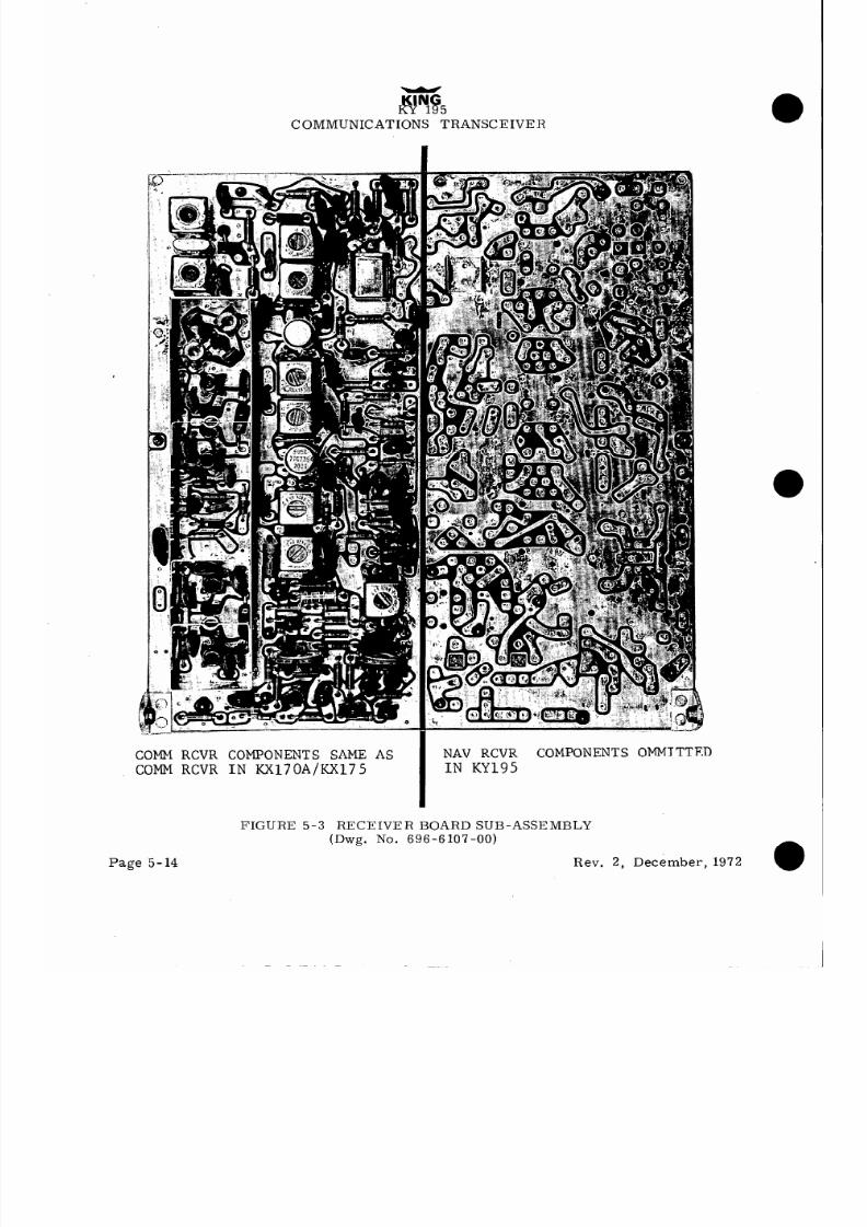
8/9/2019 KX 170A - Maintenance Manual Honeywell
http://slidepdf.com/reader/full/kx-170a-maintenance-manual-honeywell 340/586
lit%5
COMMUNICATIONS TRANSCEIVER
COMMRCVR COMPONENTSSAME AS
I
NAV RCVR COMPONENTS OMMITTED
COMM RCVR IN
KX17OA/KX175
IN KY195
FIGURE 5-3 RECEIVER BOARD SUB-ASSEMBLY
(Dwg. No. 696-6107-00)
Page .5- 14
Rev. 2, December, 1972
l

8/9/2019 KX 170A - Maintenance Manual Honeywell
http://slidepdf.com/reader/full/kx-170a-maintenance-manual-honeywell 341/586
KING
KA 47
DME CODE CONVERTER
The purpose of the King KA 47 is to convert the King KN 65 shift code obtained from the
King KX 170A/175 to the standard ARINC 2 out of 5 DME code
used in the King
KDM 700A. It is designed to be mounted next to the remote mounted DME equipment,
and pin A from 5301 should be grounded at the same point as the DME ground.
The
power requirement is either 13. 75VDC or 27. 5VDC at 225 ma.
Standard digital troubleshooting techniques may be used in troubleshooting the King
KA 47.
May, 1971
Page 1
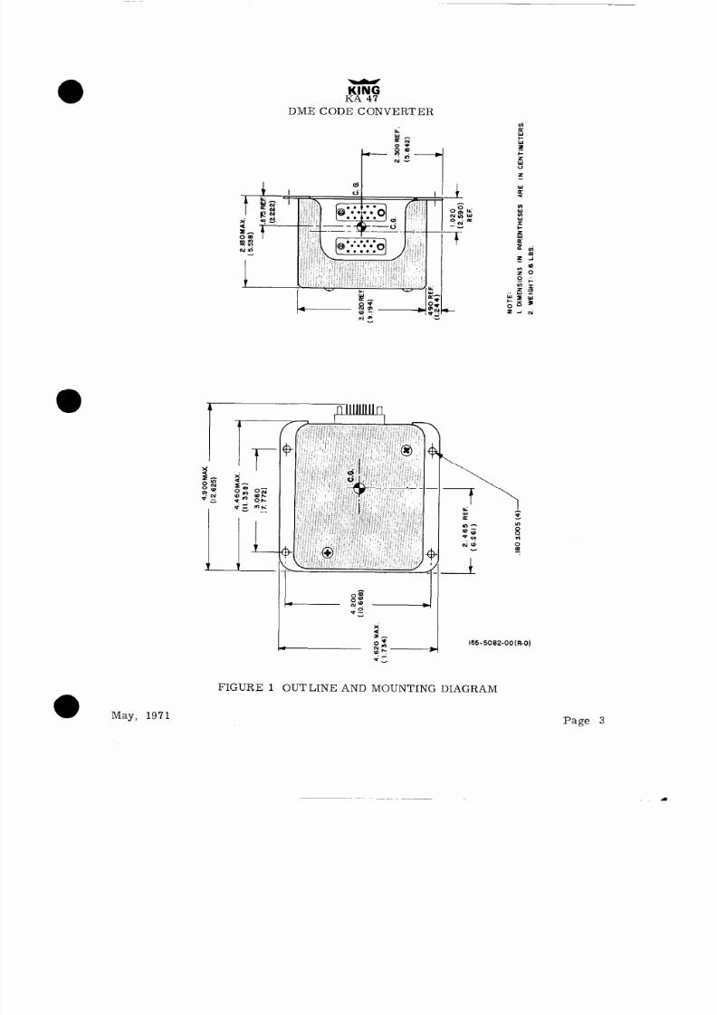
8/9/2019 KX 170A - Maintenance Manual Honeywell
http://slidepdf.com/reader/full/kx-170a-maintenance-manual-honeywell 342/586
KS
DME CODE CONVERTER
1
3:
I-
O -*
r
SF-
0,
155-5082-00(17-O)
FIGURE 1 OUTLINE AND MOUNTING DIAGRAM
May, 1971
Page 3

8/9/2019 KX 170A - Maintenance Manual Honeywell
http://slidepdf.com/reader/full/kx-170a-maintenance-manual-honeywell 343/586
KlNG
KA 47
DME CODE CONVERTER
FIGURE
2
KA 47
INTERCONNECT
DIAGRAM
(Dwg. No. 155-1102-00 R-2)
Rev.
2, December,
1972
Page 5
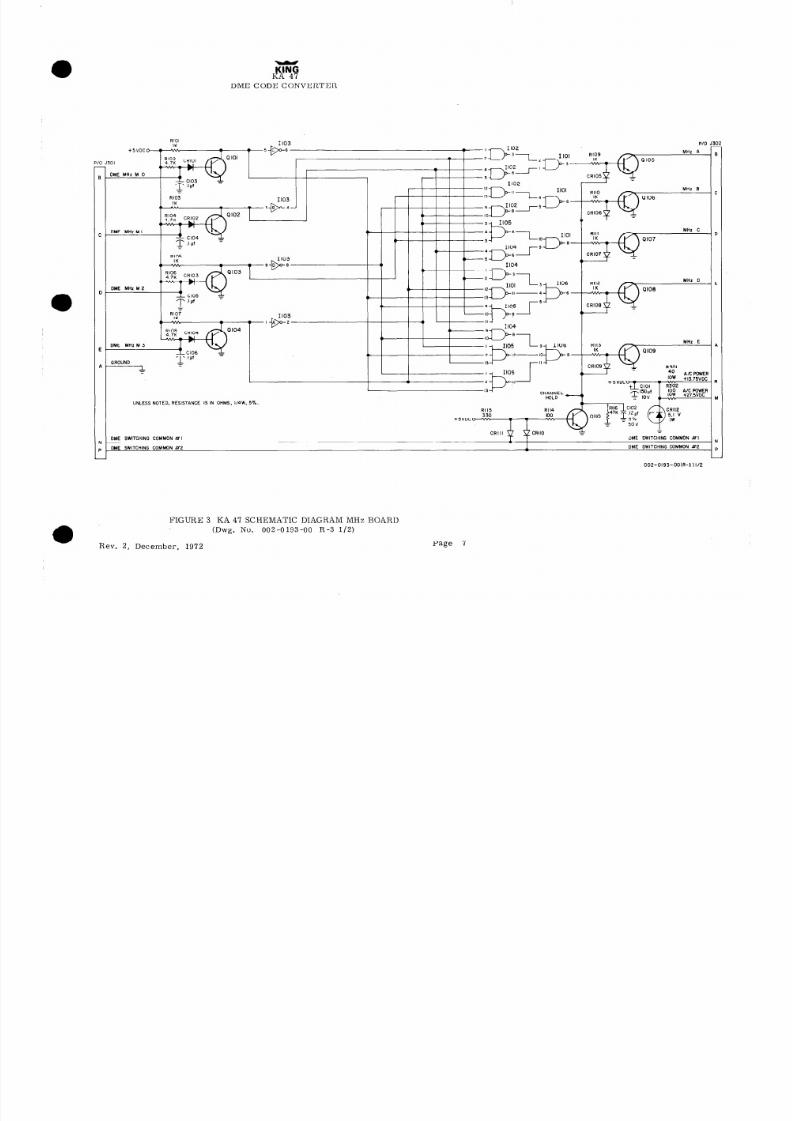
8/9/2019 KX 170A - Maintenance Manual Honeywell
http://slidepdf.com/reader/full/kx-170a-maintenance-manual-honeywell 344/586
KlNG
KA 47
DME CODE CONVERTER
‘0
-
9
C
D
E
A
N
P
-
OME MHz M I
P/O
1102
12
13
9
IO
3
4
5
4
5
II04
11-4
DME MHz M 3
GROUND
I
UNLESS NOTED, RESISTANCE 1s IN OHMS, 114w. 5%.
RI15
RI14
330
loo
+SVDC -
CRIII CRIIO
+FJQl10 i”~~,~ fp”
T
T
DME SWITCHING COMMON #I
OME SWITCHING COMMON #I
DME SWITCHING COMMON #2
LIME SWITCHING COMMON Z2
II-t-
IlG4
4,
0
MHz E
FIGURE 3 KA 47 SCHEMATIC DIAGRAM MHz BOARD
(Dwg. No. 002-0193-00 R-3 l/2)
OOZ-0193-OOIR-1)1/2
Page 7
Rev. 2, December, 1972

8/9/2019 KX 170A - Maintenance Manual Honeywell
http://slidepdf.com/reader/full/kx-170a-maintenance-manual-honeywell 345/586
$5
DME CODE CONVERTER
+SVDC
P/b J361
DME KHz K 0
RZOI
IK
R202
4.7K
CR201
a201
u
I
ti ii
7:
CR203
P203
I
t* -g
DME KHZ K 2
IV.07
0
IK
Cl204
DME KHz K 3
KHz D
1206
I
9
P206
c
KHz E
1206
R213
I
IK
II
0209
002-0193 -00 CR- 0)
NOTES: SEE SHEET I
FIGURE 4 KA 47 SCHEMATIC DIAGRAM KHz BOARD
May, 1971
Page 9

8/9/2019 KX 170A - Maintenance Manual Honeywell
http://slidepdf.com/reader/full/kx-170a-maintenance-manual-honeywell 346/586

8/9/2019 KX 170A - Maintenance Manual Honeywell
http://slidepdf.com/reader/full/kx-170a-maintenance-manual-honeywell 347/586
ASSEMBLY NO. 200 -0348 -00
DESCRIPTION MHZ CARD
UNIT KA47
REVISION 3
USED ON ASSEMBLY 071-0006-00
ASSEMBLY DRAWING NO. 300-0468 -00
PG 2
.
SYMBOL PART NUMBER DESCRIPTION QUANTITY
R112
130-0102-23
RES F/C 1K 5% QW 1
R113
130-0102-23
RES F/C 1K 50/o QW 1
R114 130-0101-23 RES F/C 100 -5% QW 1
R115 130 -033 l-23 RES F/C 330 5% QW 1
Note: R indicates Revision.
See Page 13 for New Revision and New Parts.
Page 12
Rev. 2, December, 1972

8/9/2019 KX 170A - Maintenance Manual Honeywell
http://slidepdf.com/reader/full/kx-170a-maintenance-manual-honeywell 348/586
Parts List Revision Record
Assembly No: 200-0348 -00 Manual Revision 2
ACTION
SYMBOL PART NUMBER
DESCRIPTION
QUANTITY
CHANGED CR112 007-5016-00 Diode, Zener 5. 1V 1
ADDED R116 130 -0473 -23 Res, F/C, 47K, 570, QW 1
ADDED c 102 105-0033-51 Cap., My., . 12, 50V 1
ADDED c 103 114-7 104-00 Cap., D/C lpf, 12V 1
ADDED c 104 114-7 104-00 Cap., D/C lpf, 12V 1
ADDED Cl05 114-7 104-00 Cap., D/C lpf, 12V 1
ADDED Cl06 114-7104-00 Cap., D/C lpf, 12V 1
Rev. 2, December, 1972
Page 13

8/9/2019 KX 170A - Maintenance Manual Honeywell
http://slidepdf.com/reader/full/kx-170a-maintenance-manual-honeywell 349/586
ASSEMBLY NO. 200-0349-00
DESCRIPTION KHZ CARD
UNIT KA47
REVISION 2
. USED ON ASSEMBLY 071-0006-00
ASSEMBLY DRAWING NO. 300 -0469-00
SYMBOL
PAR.T NUMBER DESCR-IPTION QUANTITY
CR201
CR202
CR203
CR204
CR205
CR206
CR207
CR208
CR209
I20 1
1202
1203
1204
1205
1206
Q20 1
Q202
Q203
Q204
Q205
Q206
Q207
Q208
Q209
R201
R.202
R203
R204
R.20 5
R206
R207
R208
R209
R210
R211
R.2 12
ti2: 3
009-5180-00
007-6016-00
007-6016-00
007-6016-00
007-60 16-00
007-6023-00
007-6023-00
007-6023-00
007,-6023-00
007-6023-00
120-0003-O 1
120-0003-01
120-0033-01
120-0001-01
120-0001-01
120 -000 1-o 1
007-0026-03
007-0026-03
007-0026-03
007-OOZS-03
007-0026-03
007-0026-03
007-0026-03
007-0026-03
007-0026-03
130-0102-23
130-0472-23
130-0102-23
130-0472-23
130-0102-23
130-0472-23
130-0102-23
130-0472-23
130-0102-23
130-0102-23
130-0102-23
130-0102-23
130-0102-23
PC BOARD
DIODE SIL lN4 154
DIODE SIL lN4154
DIODE SIL lN4154
DIODE SIL lN4154
DIODE GER lN277
DIODE GER lN277
DIODE GER lN277
DIODE GER lN277
DIODE GER lN277
INT CKT SN5410
INT CKT SN5410
INT CKT SN5404
INT CKT SN5400
INT CKT SN5400
INT CKT SN5400
TSTR SIL 2N3416
TSTR SIL 2N3416
TSTR SIL 2N3416
TSTR SIL 2N3416
TSTR SIL 2N3416
TSTR SIL 2N3416
TSTR SIL 2N3416
TSTR SIL 2N3416
TSTR SIL 2N3416
RES F/C 1K 5% QW
RES F/C 4.i’K 5% QW
RES F/C 1K 5% QW
RES F/C 4.7K 5% QW
RES F/C 1K 5% QW
R.ES F/C 4.7K 5% QW
RES F/C 1K 5% QW
RES F/C 4.7K 5% QW
RES F/C 1K 5% QW
RES F/C 1K 5% QW
RES F/C 1K 5% QW
RES F/C 1K To”/ QW
RES F/C 1K 570 QW
1
1
1
1
1
1
1
1
1
1
1
1
1
1
1
1
1
1
1
1
.1
1
1
1
1
1
1
1
1
1
1
1
1
1
1
1
1
1
PG 1
Note: R indicates Revision.
See Page 15 for Revision and New Parts.
Page 14
Rev. 2, December, 1972

8/9/2019 KX 170A - Maintenance Manual Honeywell
http://slidepdf.com/reader/full/kx-170a-maintenance-manual-honeywell 350/586
Parts List Revision Record
Assembly No: 200 -0349 -00
Manual Revision 2
ACTION
SYMBOL
PART NUMBER DESCRIPTION
QUANTITY
ADDED
c20 1 114-7 104-00
Cap.
D/C, . lpf, 12V
1
ADDED c202 114-7104-00 Cap. D/C, . lpf, 12V 1
ADDED C203 114-7104-00 Cap. D/C, . lpf, 12V
1
ADDED C204 114-7 104-00
Cap. D/C, . lyf, 12V
1
Rev. 2, December, 1972
Page 15

8/9/2019 KX 170A - Maintenance Manual Honeywell
http://slidepdf.com/reader/full/kx-170a-maintenance-manual-honeywell 351/586
PG 1
ASSEMBLY NO.
07 l-0006 -00
DESCRIPTION KA47 FINAL
UNIT KA47
REVISION 4
USED ON ASSEMBLY 07 l-0006-00
ASSEMBLY DRAWING NO.
SYMBOL PART NUMBER DESCRIPTION QUANTITY
008 -0004-00
026-0003 -00
025-0018-00
025-0018-16
025-0018-17
025-0018-18
025-0018-19
025-00 18 -20
025-0018-22
025-0018-26
025-0018-27
025-0018-28
025-0018-29
025-0018-33
025-00 18 -36
025-00 18 -37
025-00 18-38
025-0018-39
025-0018-40
025-0018-44
025-0018-46
025-0018-47
025-0018-48
025-0018-49
025-0018-57
025-0018-58
025-00 18 -98
025-0018-99
030-1007-00
047-1855-01
047-2379-00
R2
057-1379-00
076-0041-01
076 -004 l-04
076-0346-01
R2 089-2009-37
089-5907-05
089-5907-13
089-5907-20
LUG GROUND
BUSS WIRE
WIRE CW26 BLK
WIRE CW26 BRN/BLU
WIRE CW26 BRN/VIO
WIRE CW26 BRN/GRY
WIRE CW26 BRN/WHT
WIRE CW26 RED/BLK
WIRE CW26 RED
WIRE CW26 RED/BLU
WIRE CW26 RED/VI0
WIRE CW26 RED/GtiY
WIRE CW26 RED/WHT
WIRE CW26 ORN
WIRE CW26 ORN/BLU
WIRE CW26 ORN/VIO
WIRE CW26 ORN/GRY
WIRE CW26 ORN/WHT
WIRE CW26 YEL/BLK
WIRE CW26 YEL
WIRE CW26 YEL/BLU
WIRE CW26 YEL/VIO
WIRE CW26 YEL/GRY
WIRE CW26 YEL/WHT
WIRE CW26 GRN/VIO
WIRE CW26 GRN/GRY
WIRE CW26 GRY
WIRE CW26 WHT
CLIP LOCK
COVER DUST
BASE PLATE
IDENT TAG
1
. 1
1; 7
.6
.5
.6
. 5
.4
.4
. 6
.5
.6
. 5
.7
.6
. 5
.6
.5
.7
.7
.6
.5
.6
. 5
.5
.6
.9
.9
4
1
1
1
SPACER HEX 6-32 x .5”
l/2
4
SPACER HEX 6-32 x .625” 5/8
4
SPACER COVER
2
NUT 4-40 4
SCR PHP 6-32X5/16 2
SCR PHP 6-32X13/16
4
SCR PHP 6-32X1 l/4
NOTE: Rl indicates revision. See Page 18 for Rev. and New Parts
Page 16 Rev. 2, December, 1972

8/9/2019 KX 170A - Maintenance Manual Honeywell
http://slidepdf.com/reader/full/kx-170a-maintenance-manual-honeywell 352/586
PG 2
ASSEMBLY NO. 071-0006-00
DESCRIPTION KA47 FINAL
UNIT KA47
REVISION 4
USED ON ASSEMBLY 07 l-0006 -00
ASSEMBLY DRAWING NO.
SYMBOL PART NUMBER
Rl J 301
R1 J 302
R301
R302
089-6008-07
SCR FHP 4-40X7/16
089-8109-34
WASHER 4 -40
200-0348-00
MHZ CARD ASSY
200-0349-00
KHZ CARD ASSY
030-200 l-00
CONN MALE
030-2000-00
CONN FEMALE
132-O 103-09 RES 400 1OW 5%
132-0103-12
RES 10052 1OW 5%
DESCRIPTION QUaNTITY
OTE: R indicates revision. See Page 18 for Rev. and New Parts.
Rev. 2, December, 1972
Page 17

8/9/2019 KX 170A - Maintenance Manual Honeywell
http://slidepdf.com/reader/full/kx-170a-maintenance-manual-honeywell 353/586
Parts List Revision Rebord
Assembly No: 071-0006-00
Manual Revision 1
ACTION SYMBOL PART NUMBER DESCRIPTION QUANTITY
CHANGE 530 1
030 -2000 -00 Conn. Female
1
CHANGE 5302
030-2001-00 Conn. Male
1
Assembly No: 071-0006-00 (BIMRL Rev. #4) Manual Revision 2
CHANGE
057-1379-01
Ident. Tag 1
CHANGE
089-2076-30
Nut 4-40
ADDED
089-8 110-34
Washer, Lock #6
4
4
Page 18
Rev. 2, December, 1972
l
8/9/2019 KX 170A - Maintenance Manual Honeywell
http://slidepdf.com/reader/full/kx-170a-maintenance-manual-honeywell 354/586
ASSEMBLY
NO. 050 - 1239 -00
DESCRIPTION INSTALLATION KIT
UNIT KA47
REVISION 0
USED ON ASSEMBLY 050-1239-00
ASSEMBLY DRAWING NO.
PG
1
SYMBOL PART NUMBER DESCRIPTION QUANTITY
030-1008-00
LEVER & PIVOT
ASSY
4
030- 1009-00
CONN COVER
2
030-2000-00
CONN FEMALE
1
030-2001-00
CONN MALE
1
Rev. 2, December, 1972
Page 19

8/9/2019 KX 170A - Maintenance Manual Honeywell
http://slidepdf.com/reader/full/kx-170a-maintenance-manual-honeywell 355/586
KlNG
KA 47
DME CODE CONVERTER
Page 20
c.
&
200-0349-00
089-8110-34 B
(2)
132.0103.,2
I R302)
089-6008-07
089-2009-37
I41
(4)
(41
030-2000-00
(J3011
FIGURE
5
KA 47
FINAL
ASSEMBLY
(Dwg. No.
300-0470-00 R-8)( Sht. 1 of 2)
Rev.
4, Januar.y
1976

8/9/2019 KX 170A - Maintenance Manual Honeywell
http://slidepdf.com/reader/full/kx-170a-maintenance-manual-honeywell 356/586
KING
KA 47
DME CODE CONVERTER
r
KA 47
BUSS WIRE
025-0003-00
PIN A
PI16
PI01
PI02
PI03
PI04
PI05
PI06
PI07
Pi09
PIlO
PI,,
PI12
PI13
PI14
PI15
009-5179-oo-
TRANSISTOR MOUNTING
(BOTTOM VIEW)
NOTES
I
INSULATE TERMINALS OF CONNECTORS WITH HEAT SHRINKABLE
TUBING KPN-
150-0020-10 AFTER SOCDERING
2.
LACE OR TIE CABLE AT BREAK POINTS AND APPROXIMATELY .5O” INTERVALS WITH
KPN 012-1006-00.
3.
MAKE HARNESS WIRE CONNECTIONS TO SIDE OPPOSITE COMPONENTS ON BOTH PC. GOAROS.
NOTE- CRXX = CRIXX
300-0466-00
FOR COYPDNENT VALUES SEE G/M 200-03 46-00
FIGURE 6 KA 47 COMPONENT LOCATION DIAGRAM
(Dwg. No. 300-0468 -00 R-8) (Sht. 2 of 2)
Rev.
4, January, 1976 0469
NOTE - CRXX = CR2XX
300-0469-00
FOR COMPONENT \ALUES S EE B/M ZOO- 0349-00
Page 21
I
E
c
WfT NO.
FROM
)25-ODl6-33
P3D3
-16
1301 - PIN 6
-26
-PIN C
-34
- PIN D
46
- PIN E
-19
-29
-39
49
-40
-44
-57
-17
-27
-37
-47
- PIN F
1 -pPI:: l
- PIN K
- PIN P
1301 - PIN N
1301
PIN A
,302 - PIN A
- PIN 6
-PING
PIN D
- PIN E
PIN F P213
GRNGRY 6
- PIN H
P212
REDlGRY 6
-PINJ
P211
DRN/GRY 6
- PIN K
P210 YELGAY
6
-PINL P2Q9
GRN,GRY 6
-PIN N
PI 14
YEL 5
302 - PIN P PI I3 YEL/GLK 5
-99 ‘EC5
-98 ‘214
-00 :HASSIS GND
-co
:HASSIS GND.
-22 302- PIN R
-20
322 - PIN U
WIRING I
TO
7.3 HEDULE
l-
COLOR
PI16
ORN
P 103 BRN/BLU
PDl RED/BLU
PI02 ORNELU
PI04 YELIBLU
LE
:
6
6
6
P201
BRN,WHT
5
P2D3 REDIWHT 5
P2M ORNlWHT
5
P202 YE LIWHT 5
,302 PIN P YEL/BLK
1302 PIN N YEL
CMSSIS GND EL K 3
Pi12
GRN/VO 5
PI07 BRN/VO
5
PI09 RED/VI0 5
PI,0 ORN,VD
5
PIII YELVlO 5
PI05
P 106
IYE”\
p301-
P302
WHT IO
FRY ID
BLK 7
ELK a
RED
4
RED/GLK
4

8/9/2019 KX 170A - Maintenance Manual Honeywell
http://slidepdf.com/reader/full/kx-170a-maintenance-manual-honeywell 357/586
KING,
KX 170WKX175B
NAVIGATIONECEIVER
COMMUNICATIONSRANSCEIVE
INSTALLATIONANUAL
006-0085-O
REV. 1 JANUARY, 1976
8/9/2019 KX 170A - Maintenance Manual Honeywell
http://slidepdf.com/reader/full/kx-170a-maintenance-manual-honeywell 358/586
THIS EQUIPMENT MANUFACTURED UNDER
THE FOLLOWING U. S. PATENT 3,696,422

8/9/2019 KX 170A - Maintenance Manual Honeywell
http://slidepdf.com/reader/full/kx-170a-maintenance-manual-honeywell 359/586
KI
KX 170B
7
KX 175B
NAVIGATION RECEIVER/
COMMTTNICATIONS TRANSCEIVER
TABLEOF CONTENTS
SECTIONGENERALNFORMATION
Paragraph
1. 1
1.2
1.3
1.4
1. 5
1. 6
1.7
1.8
2. 1
General
2-l
2.2 Unpacking and Inspection Equipment 2-l
2.3
KX 17OB/KX 175B Installation
2-1
2.4
KA 39 Installation
2-2
2.5
Antenna Installation
2-2
2.6
Cabling
2-3
3.1
3.2
3.3
Introduction
l-l
Purpose of Equipment
l-l
Design Features
l-l
Power Requirements
l-2
Technical Characteristics
1-2
Units and Accessories Supplied
l-9
Accessories Required, but not Supplied
1-9
License Requirements
l-10
SECTION INSTALLATION
SECTIONI OPERATION
General
KX 170B/KX 175B NAV/COMM Controls
Post-Installation Checkout
3-1
3-l
3-2
SECTIONV KA47
Page
4.1
General
4-l

8/9/2019 KX 170A - Maintenance Manual Honeywell
http://slidepdf.com/reader/full/kx-170a-maintenance-manual-honeywell 360/586
KlNG
KX,170B/KX 175B
NAVIGATION RECEIVER/COMMUNICATIONS TRANSCEIVER
HISTORYOF REVISIONS
Rev. 1, January, 1976
Page
Front Page
1-9
2-1
Paragraph 2.3(b) changed
2-4A
Antenna Cable Assembly added
2-8A
Drawing of cooling diffuser added
2-8B
Installation drawing of Ram Air Kit added
2-9
Interconnect updated
2-13
Interconnect updated
2-17 Interconnect updated
2-19
Interconnect updated
Reason for Change
Rev. No. change and Warranty deleted
Part Number changes

8/9/2019 KX 170A - Maintenance Manual Honeywell
http://slidepdf.com/reader/full/kx-170a-maintenance-manual-honeywell 361/586
KlNG
KX 170B/KX 175B
NAVIGATION RECEIVER /
COMMUNICATIONS TRANSCEIVER
SECTION
GENERALNFORMATION
1.1 INTRODUCTION
This manual contains information relative to the physical, mechanical and electrical characteristics
of the King Radio Corporation Silver Crown KX 170B/KX 175B, and interconnect information for
various NAV/COMM system options.
1.2 PURPOSE F EQUIPMENT
The King KX 170B / KX 175B NAV/COMM combines in a single panel mounted unit a 720 channel
VHF COMM Transceiver and an independent 200 channel VHF NAV receiver. The NAV Receiver
supplies VOR/LOC information to navigational converters and provides frequency selection for
remote mounted Distance Measuring Equipment and Glideslope Receivers.
1.3 DESIGN EATURES
1.3. 1
KX 170B/KX 175B
A.
Controls
1.
On-Off switches are independent of volume control settings allowing the volume
to remain at desired levels.
2.
Separate NAV and COMM ON-OFF switches (KX 175B NAV and COMM are
electrically independent).
3.
Automatic squelch eliminates pilot responsibility for continuously monitoring
squelch adjustments. Squelch threshold automatically adjusts to open on
readable signals. Test position opens squelch to test COMM receiver sensi-
tivity and to listen to extremely weak signals.
4.
Ident-Voice switch filters station ident from receiver audio.
5.
Frequency selector mechanism features human engineered concentric
airline type drum readout, and blue-white .
Glideslope and DME switching is
provided.
B.
Electronics
1.
Varactor diode tuned filters eliminate use of mechanical tuning shafts and
mechanisms.
2.
Balanced mixers for superior intermodulation, cross modulation, and L. 0.
radiation performance provide true 1 + I operation.
3.
Transistorized transmitter provides 5 watts minimum output power and long
term reliability superior to tube designs,
4.
The digital frequency synthesizers utilize state of the art integrated circuits
to replace all but 6 crystals (KX 170B) and 7 crystals (KX 175B), providing
improved mean time between failure.
Page l-l

8/9/2019 KX 170A - Maintenance Manual Honeywell
http://slidepdf.com/reader/full/kx-170a-maintenance-manual-honeywell 362/586
KlNG
KX 17OB/KX 175B
NAVIGATION RECEIVER /
COMMUNICATIONS TRANSCEIVER
5. Crystal filter selectivity both NAV and COMM.
6.
Carrier to noise squelch with carrier squelch back up functionally described
above.
7.
Tight AGC (typically 0. 5db from 10~~ to 20,000~~) minimizes audio level
variations.
C.
Construction
1.
Modular construction for ease of maintenance.
2.
Rack mounted, removable from the front panel.
3.
Anti-theft locking mechanism. (Optional)
4.
Provisions for identifying radios as COMM 1, NAV 1 and COMM 2, NAV 2 in
dual installations.
1.4 POWER EQUIREMENTS
The KX 170B/KX 175B requires 13.75 volts for proper operation.
Aircraft having electrical
power plants producing 27. 5 volts require the installation of a voltage converter.
The KA 39
Voltage Converter, designed to separately convert NAV and COMM 27. 5 volts to 13. 75 \,olts, may
be conveniently remote mounted in the aircraft.
1.5 TECHNICALHARACTERISTICS
KX 170B TRANSCEIVER
PECIFICATION
CHARACTERISTIC
GENERAL
IOUNTING :
Panel mounted, no shock mounting required.
;IZE KX 170B NAV/COMM
6.3 12 X2. 600X14. 15 inches w/connectors.
(16.03X6. 60X35. 94 centimeters. )
{EIGHT :
KX 170~ NAV/COMM
7.0 lbs excluding external connectors and
harness.
(3. 18Kg)
OWER REQUIREMENTS:
COMM Receive
COMM Transmit (Tone)
NAV Receiver
Lamps
Max Total Current
13. 75V (or 27. 5V with KA 39)
0.70 amps
4. 5 amps (2.8 amps unmodulated)
0. 52 amps
0. 16 amps (13. 75Vdc), 0.08 amps (27. 5Vdc)
5. 1 amps (Transmit tone mod, NAV Rec.
Lamps)
Page l-2

8/9/2019 KX 170A - Maintenance Manual Honeywell
http://slidepdf.com/reader/full/kx-170a-maintenance-manual-honeywell 363/586
KlNG
KX 170B/KX 175B
NAVIGATION RECEIVER /
COMMUNICATIONS TRANSCEIVER
KX 170B TRANSCEIVER
SPECIFICATION
CHARACTERISTIC
COMM TRANSCEIVER
CRYSTAL CONTROLLED:
FREQUENCY RANGE:
FREQUENCY STABILITY:
720 channels
118.000 to 135. 975MHz with 25kHz spacing
*0.003%
TRANSMITTER
VHF POWER OUTPUT:
MODU LATION :
5 watts minimum, 50 ohm load
85% modulation capability with 90% limiting
provided
MICROPHONE:
Dynamic mike containing transistorized pre-
amp or carbon (must provide at least 120
mVRMS into 5000 load. )
SIDETONE :
DUTY CY C LE :
Adjustable up to 4mw into 500 ohm headphones
1 minute on, 4 minutes off (20%)
RECEIVER
SENSITIVITY:
SELECTIVITY:
SPURIOUS RESPONSES:
SQUELCH:
1. 51.l~ (s-o-f?will provide a 6db minimum
signal plus noise to noise ratio ( lkHz, 3070
mod)
Typical 6db at f8kHz, 60db at f35kHz
Down at least 60db
Automatic squelch (carrier to noise) with
manual disable and carrier squelch override.
AGC C HARAC TERISTICS :
From 10~~ to 20, 000~~ audio output will not
vary more than 3db.
NAV RECEIVER
ZRYSTAL CONTROLLED:
FREQUENCY RANGE:
SENSITIVITY:
Navigation
200 channels.
108.00 to 117. 95MHz with 5OkHz spacing.
1. 51.r~ (soft) will provide a half-flag indication
1. Opv (soft) will provide a 6db signal + noise
noise
ratio.
Page l-3

8/9/2019 KX 170A - Maintenance Manual Honeywell
http://slidepdf.com/reader/full/kx-170a-maintenance-manual-honeywell 364/586
KlNG
KX 170B/KX 175B
NAVIGATION RECEIVER /
COMMUNICATIONS TRANSCEIVER
KX 170B TRANSCEIVER
SPECIFICATION
CHARACTERISTIC
SELECTIVITY :
Typical 6db at k19kHz
50db at f50kHz
SPURIOUS RESPONSES:
Down at least 60db
IDENT FILTER:
Tone rejection, 15db, minimum
AGC CHARACTERISTICS:
From 10~~ to 20,000~~ audio output will not
vary more than 3db.
NAV RECEIVER ACCURACY:
Two sigma limit, +l. 5”
NAV OUTPUT:
With LOC adjusted for 0.3 5Vrms, VOR = 0. 5
Vrms (typical) into 2OKfi or greater load
impedance.
DME CHANNELING:
I
MO Ml M2 M3
Kg Kl K2 K3
108 - - 0 -
.
ox 0 0 - -
. x0
109 - - - 0
.1x 0 0 0 - . .x5 0
110 0 - - -
.2x 0 0 0 0
111 0 0 - -
.3x - 0 0 0
112 0 0 0 -
.4x - - 0 0
113 - 0 0 0
.5x 0 - - 0
114 0 - 0 0
.6X - 0 - -
115 - 0 - 0
.7x - - 0 -
116 0 - 0 -
.8X - - - 0
117 0 0 - 0
.9x 0 - - -
NOTE: (-) = OPEN, (0) = DME COMMON.
ILS ENERGIZE :
The ILS energize wire is connected to the ILS
common wire when the MHz selector is in
either the 108, 109, 110, or 111 position
AND SIMULTANEOUSLY the kHz selector is ir
either the 0. 10, 0. 15, 0. 30, 0.35, 0. 50, 0. 55
0. 70, 0. 75, 0. 90 or 0.95 position.
I
Page l-4

8/9/2019 KX 170A - Maintenance Manual Honeywell
http://slidepdf.com/reader/full/kx-170a-maintenance-manual-honeywell 365/586
KlNG
KX l’IOB/I(X 175B
NAVIGATION RECEIVER /
COMMUNICATIONS TRANSCEIVER
SPECIFICATION
GLIDESLOPE CHANNELING:
GS GS GS GS
108 109 110 111
108 0 - - -
109 - 0 - -
110 - - 0 -
111 - - - 0
112 - - - -
113 - - - -
114 - - - -
115 - - - -
116 - - - -
117 - - - -
1 C HARAC TE RI STIC
I
GS GS GS GS GS
0.1 0.3 0.50.7 0.9
.
ox - - - - -
.1x 1 - - - -’
.2x
- - - - -
.3x - 1 - - -
.4X - - - - -
.5x - - 1 - -
.6X _ - _ _ -
.7x - - - 1 -
.8X _ _ _ _ _
.9x - - - - 1
NOTE :
(0) = ILS common, (-) = open, (1) = either KN 73 A+ (KN 73 Installations)
or KX l’i’OB/KX 175B A+ with lK0 source resistance (KI 2 11C /KI 2 12/KI 213 /
KI 2 14 installations).
I
AUDIO
4UXILIARY AUDIO INPUTS:
Two (2) 500 ohms with 30db isolation between
any two.
[NTERCOM INPUT:
One (1) Intercom Microphone Input. (Micro-
phone must provide at least 120m Vrms into
5OOfl load).
FREQUENCY RESPONSES:
HEADPHONE OUTPUT:
SPEAKER OUTPUT:
Within 6db from 350Hz to 2500Hz.
50mw into 500 ohm
4.5Vrms into auxiliary input produces 5 watts
audio output.
KX 175B TRANSCEIVER
IS0 COMPLIANCE:
C OMM Transmit
COMM Receive
VOR
LOC
Environmental
MOUNTING:
SIZE:
C37b (00-110, Class II)
C38b (DO-109)
C40a (DO-114)
C36c (00-131, Class C)
DAPBAAXXXXXX
Panel mounted, no shock mounting required.
6.3 12 X 2.600 X 14. 15 inches w/connectors.
(16.03 X 6.60 X 35. 94 centimeters)
WEIGHT :
7.0 lbs excluding external connectors and
harness. (3. 18Kg)
Page l-5
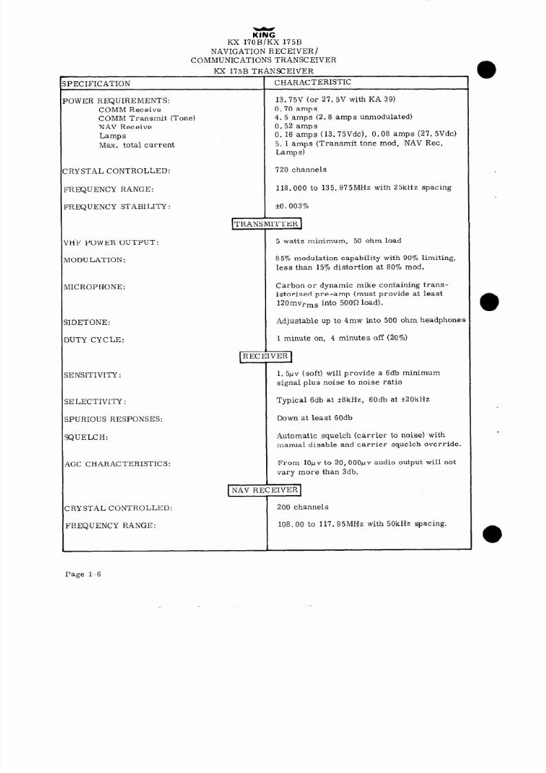
8/9/2019 KX 170A - Maintenance Manual Honeywell
http://slidepdf.com/reader/full/kx-170a-maintenance-manual-honeywell 366/586
KlNG
KX 170B/KX 175B
NAVIGATION RECEIVER /
COMMUNICATIONS TRANSCEIVER
KX 175B TRANSCEIVER
PECIFICATION
CHARACTERISTIC
OWER REQUIREMENTS:
13.75V (or 27. 5V with KA 39)
COMM Receive
0.70 amps
COMM Transmit (Tone) 4. 5 amps (2.8 amps unmodulated)
NAV Ret eive
0.52 amps
Lamps
0. 16 amps (13.75Vdc), 0.08 amps (27. 5Vdc)
Max. total current
5. 1 amps (Transmit tone mod, NAV Ret,
Lamps)
RYSTAL CONTROLLED:
‘REQUENCY RANGE:
‘REQUENCY STABILITY :
720 channels
118.000 to 135. 975MHz with 25kHz spacing
*o. 003%
TRANSMITTER
‘HF POWER OUTPUT:
‘IODU LATION:
5 watts minimum, 50 ohm load
85% modulation capability with 90% limiting,
less than 15% distortion at 80% mod.
IICROPHONE:
IDETONE :
)UTY CY C LE :
Carbon or dynamic mike containing trans-
istorized pre-amp (must provide at least
120 mVrmS
into 50052 load).
Adjustable up to 4mw into 500 ohm headphones
1 minute on, 4 minutes off (2OoJo)
I
RECEIVER
ENSITIVITY :
1. 511~ (soft) will provide a 6db minimum
signal plus noise to noise ratio
#ELECTIVITY :
SPURIOUS RESPONSES:
QUELCH:
Typical 6db at f8kHz, 60db at f20kHz
Down at least 60db
Automatic squelch (carrier to noise) with
manual disable and carrier squelch override.
LGC CHARACTERISTICS:
From 10~~ to 20,000~~ audio output will not
vary more than 3db.
NAV RECEIVER
:RYSTAL CONTROLLED:
200 channels
;‘REQUENCY RANGE:
108.00 to 117. 95MHz with 50kHz spacing.
Page l-6

8/9/2019 KX 170A - Maintenance Manual Honeywell
http://slidepdf.com/reader/full/kx-170a-maintenance-manual-honeywell 367/586
KlNG
KX 170B/KX 175B
NAVIGATION RECEIVER /
COMMUNICATIONS TRANSCEIVER
KX 175B TRANSCEIVER
lPECIFICATION
iENSITIVITY :
Navigation
;E LEC TIVITY :
lPURIOUS RESPONSES:
DENT FILTER:
LGC CHARACTERISTICS
1CCURACY:
JAV OUTPUT
)ME CHANNELING:
CHARACTERISTIC
1. 51.t~ (soft) will provide a half-flag indication
1.0,~~ (soft) will provide a 6db signal + noise
noise
Typical 6db at +lSkHz
75db at *50kHz
Down at least 60db
Tone rejection, 15db, minimum
From 10~~ to 20, 000~~ audio output will not
vary more than 3db
Two sigma limit, +l. 0”
With LOC adjusted for 0.35Vrms, VOR =
0. 5Vrms (typical) into 20Kn or greater load
impedance.
MO Ml M2 M3
108 - - 0 -
109 - - - 0
110 0 - - -
111 0 0 - -
112 0 0 0 -
113 - 0 0 0
114 0 - 0 0
115 - 0 - 0
116 0 - 0 -
117 0 0 - 0
. ox
. 1x
.2x
. 3x
.4x
.5x
.6X
.7x
.8X
.9x
Kg Kl K2 K3
50kHz
0 0 - - . x0
1
0 0 0 - . x5 0
0 0 0 0
0 0 0
-
-
0 0
0 - - 0
0 -
- - 0 -
-
- -
0
0 - - -
NOTE: (-) = OPEN, (0) = DME COMMON.
LS ENERGIZE:
The ILS energize wire is connected to the ILS
common wire when the MHz selector is in
either the 108, 109, 110, or 111 position
AND SIMULTANEOUSLY the kHz selector is
in either the 0. 10, 0. 15, 0. 30, 0.35, 0. 50,
0. 55, 0. 70, 0. 75, 0. 90 or 0. 95 position.
1
Page l-7

8/9/2019 KX 170A - Maintenance Manual Honeywell
http://slidepdf.com/reader/full/kx-170a-maintenance-manual-honeywell 368/586
KlNG
KX 170B/KX 175B
NAVIGATION RECEIVER /
COMMUNICATIONS TRANSCEIVER
KX 175B TRANSCEIVER
SPECIFICATION
CHARACTERISTIC
SLIDESLOPE CHANNELING:
GS GS GS GS GS GS GS GS GS GS
108 109 110 111 0.1 0.3 0.5 0.7 0.9 5OkHz
108 0 - - -
ox - - - - -
. x0 -
109 - 0 - -
. 1x
1 - - - -
. x5 0
110 - - 0 -
.
2x
- - - - -
111 - - - 0
.
3x -l---
112 - - - -
.
4X
- - - - -
113 - - - -
.
5x
- - 1- -
114 - - - -
(5X - - _ _ -
115 - - - - .7x - - - 1 -
116 - - - -
.8X -___-
117 - - - -
.9x ----1
NOTE: (0) = ILS common, (-) = open, (1) = either KN 73 A+ (KN 73 Installations) or
KX 170B. KX 175B A+ with 1KR source resistance (KI 211C /KI 212/KI 2 13 /
KX 2 14 installations).
AUDIO
AUXILIARY AIJDIO INPUTS:
Two
(2)
500 ohms with 30db isolation between
any two.
NTERCOM INPUTS:
One (1) Intercom Microphone Input.
(Microphone must provide at least 120mv
into 5000 load.
TREQUENCY RESPONSES:
HEADPHONE OUTPUT:
SPEAKER OUTPUT:
Within 6db from 350Hz to 2500Hz.
50mw into 500 ohm
4. 5Vrms into auxiliary input produces 5 watts
audio output.
SIZE:
KA 39 VOLTAGE CONVERTER
3. 500 X 2.000 X 5. 500 inches
(8.889 X 5. 18 X 13.87 centimeters)
WEIGHT :
POWER:
1. 1 lbs. excluding harness (. 5Kg)
A
B
Input Volts 27. 5vdc 27. 5vdc
output Volts 13. 75vdc 13.75vdc
(nominal)
(nominal)
Input Current continuous
Input Current 40% duty
---------
Output Current continuous 1. 5A
0.75A
Output Current 40% duty 5. OA
---------
Page l-8

8/9/2019 KX 170A - Maintenance Manual Honeywell
http://slidepdf.com/reader/full/kx-170a-maintenance-manual-honeywell 369/586
KlNG
KX 170B/KX 175B
NAVIGATION RECEIVER /
COMMUNICATIONS TRANSCEIVER
1.6 UNITSAND ACCESSORIESUPPLIED:
A.
King KX 170B NAV/COMM (069-1020-00)
B. King KX 175B NAV/COMM (069-1019-00)
C.
King KX 170B/KX 175B Installation Kit (050-1142-00) includes:
030-0101-00
030 - 10 19 -00
030-2101-04
047 - 1743 -0 1
047- 185 l-00
057-1214-00
057-1214-01
057-1214-02
057-1214-03
088-0136-01
089-2188-22
089-5523-05
089-5903-05
089-5907-05
089-6008-04
089-8025-30
089-8094-30
090-0019-07
Connector, Antenna (TED g-30-4)
Clamp, Cable Hall
Connector, 42 pin (Amphenol 26- 190 -42)
Plate, Connector Mounting
Cover, Connector Mounting Plate
Decal, COMM 1
Decal, COMM 2
Decal, NAV 1
Decal, NAV 2
Filter, Red Lamp
E4 ESNA Nut
Screw, #4-40 X 5/16 Fil HP
Screw, #4-40 X 5/16 PHP
Screw, #6-32 X 5/16 PHP
Screw, #4-40 X l/4 FHP
Flat Washer
Flat Washer
Ring, Retainer
2
2
1
1
1
1
1
1
1
2
2
4
2
2
4
2
2
2
1.7 ACCESSORIESEQUIRED,UTNOTSUPPLIEDr
A. Communication and navigation antenna and cables.
B.
Headphones and speaker:
1.
Headphones: Low impedance types, 300 to 1,000 ohms.
2.
Speaker: Voice coil impedance 3 to 6 ohms nominal.
C.
KA 39 Voltage Converter, 27. 5V to 13.75V (required in 27. 5V installation only).
D.
Microphone: Low impedance carbon, or dynamic with transistor preamp, such as
King KA 14.
E. VOR / LOC converter and indicator. Various King Options include:
1.
KI 20 1C VOR Indicator (VOR/LOC only)
2.
KI 2 14 ILS Indicator (VOR / LOC Glideslope 40 Channel)
3. (4
(b)
KN 77 VOR/LOC Converter, with KNI 520 Navigation Indicator
KN 77 VOR/LOC Converter, with KPI 550A Pictorial Navigation System
Rev. 1, January, 1976
Page l-9

8/9/2019 KX 170A - Maintenance Manual Honeywell
http://slidepdf.com/reader/full/kx-170a-maintenance-manual-honeywell 370/586
4. (a)
(b)
5. (a)
(b)
1.8 LICENSE EQUIREMENTS
KX 170B/KX 175B
NAVIGATION REC EIVER /
COMMUNICATIONS TRANSCEIVER
KN 73 Glideslope Receiver -
KN 77 VOR/LOC Converter with KNI 520
Navigation Indicator
KN 73 Glideslope Receiver - KN 77 VOR/LOC Converter with KPI 550
Pictorial Navigation System
KN 74 Area Navigation Computer with KI 2 13 C DI and Glideslope
Receiver.
KN 74 Area Navigation Computer with KN73 Glideslope Receiver
and KPI 5’50A Pictorial Navigation System.
The Federal Communications Commission requires that the operator of the transmitter of this
equipment holds a Restricted Radio Telephone Operator Permit, or higher class license. A
permit may be obtained by a U. S. citizen from the nearest field office of the FCC; no examination
is required.
This equipment has been type accepted by the FCC and entered on their list of type accepted
equipments as King KX 170B/KX 175B and must be identified as King KX 170B or King KX 175B.
-CAUTION -
The VHF transmitter in this equipment is guaranteed
to meet Federal Communications Commiss ion approval
only when King crystals are used.
Use of other than King crystals is considered an un-
authorized modification.
Page l-10

8/9/2019 KX 170A - Maintenance Manual Honeywell
http://slidepdf.com/reader/full/kx-170a-maintenance-manual-honeywell 371/586
KlNG
KX 170B/KX 175B
NAVIGATION RECEIVER /
COMMUNICATIONS TRANSCEIVER
SECTIONI
INSTALLATION
2.1 GENERAL
This section contains suggestions and factors to consider before installing the KX 170B/KX 175B
NAV/COMM unit and KA 39 Voltage Converter (27. 5V installations only).
Close adherence to
these suggestions will assure a more satisfactory performance from the equipment.
;Zf”OAPACKING ND INSPECTINGQUIPMENT
Exercise extreme care when unpacking each unit. Make a visual inspection of each unit for evi-
dence of damage incurred during shipment.
If a claim for damage is to be made, save the shipping
container to substantiate the claim.
When all equipment is removed, place in the shipping contain-
er all packing materials for use in unit storage or reshipment.
The KX 170B/KX 175B installation
will conform to standards designated by the customer,
installing agency and existing conditions as
to unit location and type of installation.
J.3 KX 170B/KX 1758 INSTALLATION
Listed below are factors and suggestions to consider before installing your KX 170B/KX 175B
system. Close adherence to these suggestions will assure more satisfactory performance from
your equipment.
(4
The KX 170B/KX 175B is mounted rigid in the aircraft panel. Mark and cut the mounting
hole as shown in Figure 2-5.
The purpose of the “behind aircraft panel mount cutout is
to allow a margin of error in cutout size and prevent the mounting tray front edge from
being visible.
The mounting tray bottom lip should extend through the mounting hole
flush with the instrument panel to insure proper plug pin engagement.
(b) Avoid mounting close to any high external heat source. Forced air cooling should be
supplied for 3 or more radios in a stack.
(cl
Remember to allow adequate space for installation of cables and connectors.
(4
Secure the mounting rack to instrument panel per Figure 2-5.
The rear mounting bosses
should be attached to the airframe by means of support brackets.
(e)
Slide the KX 170B /KX 175B into the rack and secure by turning the locking screw on the
front panel.
-CAUTION -
Do not force locking tab screw.
An antitheft mechanism is available for the KX 170B/KX 175B (KPN 050-1326-00 short
locking bar, 050 -1326-O 1, long locking bar). This k it may be installed at the customer’s
option to provide a means of locking the radio to the instrument panel with a padlock
located on the lower rear corner of the mounting tray.
Installation consists of riveting the bracket to the mounting tray as shown in Figure 2-5.
After the radio installation is complete,
the locking bar may be inserted and a small
padlock affixed to deter theft.
Rev. 1, January, 1976
Page 2-l

8/9/2019 KX 170A - Maintenance Manual Honeywell
http://slidepdf.com/reader/full/kx-170a-maintenance-manual-honeywell 372/586
KlNG
KX 170B/KX 175B
NAVIGATION RECEIVER /
COMMUNICATIONS TRANSCEIVER
(d
The installing agency will supply and fabricate all external cables.
The plugs required
are supplied by King Radio.
2.4 KA 39 INSTALLATION
(For use in 27. 5 volt installations only)
(a)
Select the KA 39 location considering good thermal conductivity to the airframe, con-
venient cable rounting.and separation from other heat sources,
The KA 39 shsuld be
mounted no closer to the KX 170B/KX 175B than is necessary to good ther ma1 isolation.
(b)
Refer to Figure 2-4 for the KA 39 mounting dimensions.
Cc)
Secure the KA 39 firmly in place.
Cd)
The installing agency will supply and fabricate external cables.
2.5 ANTENNANSTALLATION
(4
Conventional 50 ohm horizontally polarized NAV and vertically polarized COMM antennas
are required with the KX 170B/KX 175B. Vertical bent whip antennas are not recommend-
ed.
Wideband COMM antennas provide efficient operation over the COMM band.
Antennas
should be installed per manufacturers recommendations.
Additional recommendations
are as follows:
COMM ANTENNA
1.
Mount antenna on flat metal surface or install a ground plane a t least 18 inches
square.
2.
The antenna should be well removed from any projections and the engine(s) and
propeller.
3.
NAV and COMM Antennas must be well separated to minimize COMM interfer-
ence to NAV while transmitting,
(Minimum recommended separation is 30db).
NAV ANTENNA
1.
The location should be well removed from other antenna, projections and
engine(s).
It should have a clear line of sight area if possible.
2.
The antenna MUST BE mounted symmetrically with the centerline of the air-
craft.
3.
Avoid running other coaxial cables and wires with the NAV antenna cable.
(b)
The antenna connectors on the KX 170B/KX 175B unit are identified on the rear die
casting.
Page 2-2
Rev. 1, January, 1976
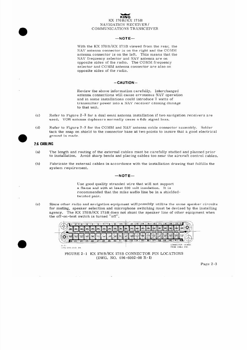
8/9/2019 KX 170A - Maintenance Manual Honeywell
http://slidepdf.com/reader/full/kx-170a-maintenance-manual-honeywell 373/586
KlNG
KX 17OB/KX 175B
NAVIGATION RECEIVER /
COMMUNICATIONS TRANSCEIVER
-NOTE-
With the KX 170B/KX 175B viewed from the rear, the
NAV antenna connector is on the right and the COMM
antenna connector is on the left. This means that the
NAV frequency selector and NAV antenna are on
opposite sides of the radio.
The COMM frequency
selector and COMM antenna connector are also on
opposite sides of the radio.
-CAUTION-
Review the above information carefully. Interchanged
antenna connections will cause erroneous NAV operation
and in some installations could introduce 7 watts of
transmitter power into a NAV receiver causing damage
to that unit.
(c)
Refer to Figure 2-3 for a dual omni antenna installation if two navigation receivers are
used.
VOR antenna duplexers normally cause a 6db signal loss.
(d
Refer to Figure 2-2 for the COMM and NAV antenna cable connector assembly. Solder
tack the snap on shield to the connector base at two points to insure that a good electrical
ground is made.
2.6 CABLING
(a)
(b)
(c)
The length and routing of the external cables must be carefully studied and planned prior
to installation. Avoid sharp bends and placing cables too near the aircraft control cables.
Fabricate the external cables in accordance with the installation drawing that fulfills the
system requirement.
-NOTE-
Use good quality stranded wire that will not support
a flame and with at least 600 volt insulation. It is
recommended that the mike audio line be in a shielded-
twisted pair.
Since other radio and navigation equipment will possibly utilize the same speaker circuits
for muting, speaker selection and microphone switching must be devised by the installing
agency. The KX 170B/KX 175B does not shunt the speaker line of other equipment when
the off-on-test switch is turned “off”.
Plil
I
CONNECTORIEHED
<PN 30-2101-04
FROMAKE ND.
FIGURE 2-l KX 170B/KX 175B CONNECTOR PIN LOCATIONS
(DWG. NO. 696-6002-00 R-l)
Page 2-3

8/9/2019 KX 170A - Maintenance Manual Honeywell
http://slidepdf.com/reader/full/kx-170a-maintenance-manual-honeywell 374/586
KlNG
KX 170B/KX 175B
NAVIGATION RECEIVER /
COMMUNICATIONS TRANSCEIVER
Page 2-4
Trim coax cable outer insulation as shown.
/SOLDER
Fold braid back over outer cover of coax.
Do not cross strands.
Solder center conductor to center pin of
conductor.
Make sure front end of braid
(Point of fold) is even with bottom of connector
(Shown by arrows)
Slide connector cap,
with clearance hole in
position to clear dielectric, on to connector
until it snaps in place.
Push braid forward and flatten against connector
cap and solder.
Solder tat connector cap to connector in at least
two places to insure good electrical contact.
FIGURE 2-2 ANTENNA CABLE ASSEMBLY
(DWG. NO. 696-6003 -00)
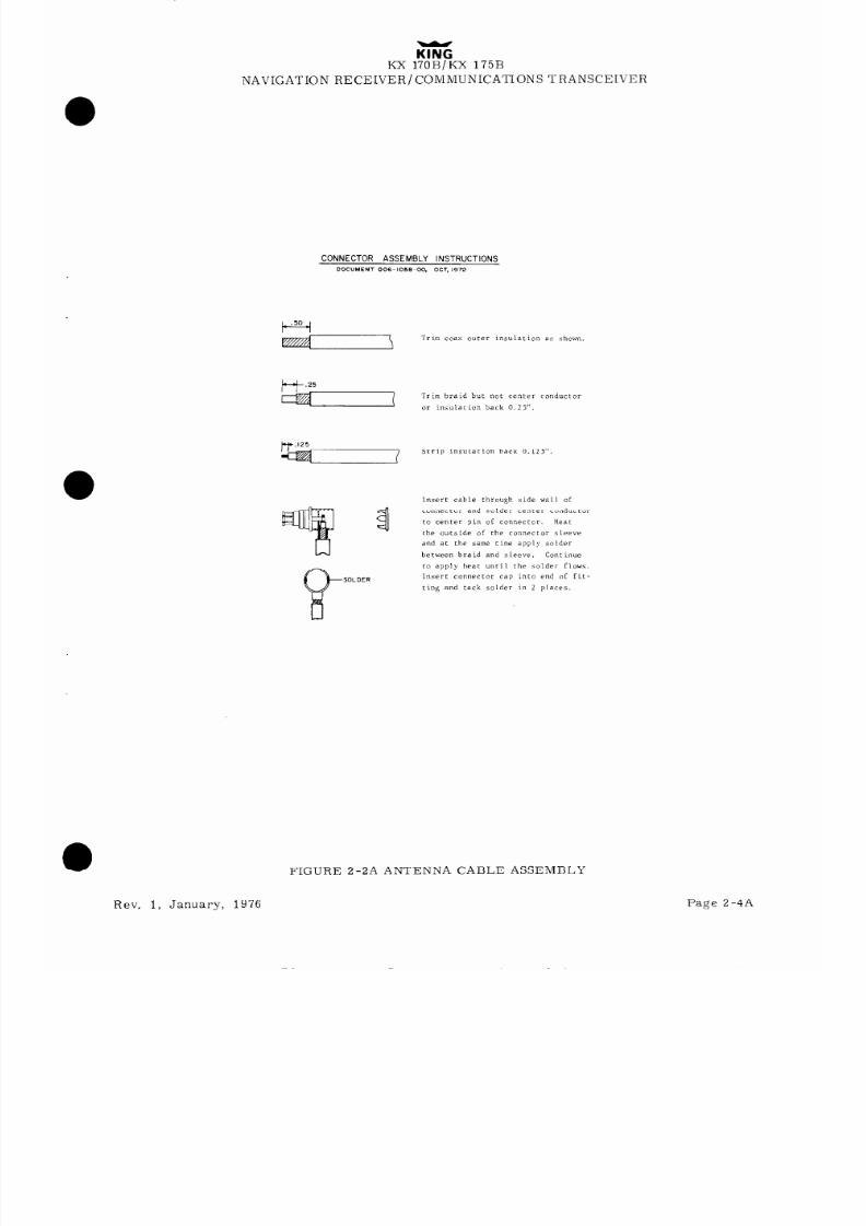
8/9/2019 KX 170A - Maintenance Manual Honeywell
http://slidepdf.com/reader/full/kx-170a-maintenance-manual-honeywell 375/586
KlNG
KX 170B/KX 175B
NAVIGATION RECEIVER/COMMUNICATIONS TRANSCEIVER
CONNECTOR ASSEMBLY INSTRUCTIONS
DOCUMENT 006-1058-00. OCT. 1972
Trim braid but noe center conductor
or insuhiion back 0.25”.
Strip insulation back 0.125”
Insert cable through side wall of
connector and solder center conductor
to center pin of connector. tleac
the oueside of the connector sleeve
and at the same rime apply solder
between braid and sleeve. Cant inue
to apply heat until the solder flows.
Insert connector cap into end of fit-
ting and tack solder in 2 places.
FIGURE 2-2A ANTENNA CABLE ASSEMBLY
Rev. 1, January, 1976
Page 2-4A

8/9/2019 KX 170A - Maintenance Manual Honeywell
http://slidepdf.com/reader/full/kx-170a-maintenance-manual-honeywell 376/586
KlNG
KX 170B/KX 175B
NAVIGATION RECEIVER /
COMMUNICATIONS TRANSCEIVER
FIGURE 2-3 DUAL OMNI ANTENNA INSTALLATION
(DWG. NO. 696-6005-00)
Page 2-5

8/9/2019 KX 170A - Maintenance Manual Honeywell
http://slidepdf.com/reader/full/kx-170a-maintenance-manual-honeywell 377/586
KlNG
KX 17OB/KX 175B
NAVIGATION RECEIVER /
COMMUNICATIONS TRANSCEIVER
USE#B PAN. HO. SCREWS
NOTES:
I. ALL DIMENSIONS IN PARENTHESIS ARE IN CENTIMETERS.
2.WEIGHT: I.1 Ibs
3 TERMINALS WILL TAKE 16TOZZAWG WIRE
4 TERMINALS ARE tf5-40x14 BD. HD. SCREWS
WARNING
-
OONOT MOUNT IN CLOSE PROX IMITY
TO HEATER DUCT OR OTHER SOURCES OF HEAT
FIGURE 2-4 KA 39 VOLTAGE CONVERTER OUTLINE AND MOUNTING DRAWING
(DWG. NO. 155-5076-00 R- )
Page 2-6

8/9/2019 KX 170A - Maintenance Manual Honeywell
http://slidepdf.com/reader/full/kx-170a-maintenance-manual-honeywell 378/586
KlNG
KX 17OB/KX 175B
NAVIGATION RECEIVER /
COMMUNICATIONS TRANSCEIVER
. CUTOUT DIMENSIONS FOR
gg
BEHIND AIRCRAFT PANEL MOUNT
ci ‘D
CUTOUT DIMENSIONS FOR
FRONT AIRCRAFT PANEL MOUNT
I
NOTES:
I DIMENSIONS IN PARENTHESIS ARE IN CENTIMETERS
2. WEIGHT: 7.0LBSf3.2 K91
0
0
7
C
3.100
(787)
L
/
4
I @-
3
L
-ZlB f.55) DIA. I PLC.
(LOCKING PIN HOLE)
- 1.650
(4.191
.I87 t47) DIA., 6 PLACES
3 IN lNSTALLATlONS INVOLVING 2 OR MORE KING SILVERCROWN UNITS
STACKED VERTICALLY, IT IS POSSIBLE TO SPOTWELD THE MOUNTNG
TRAYS TOGETHER PRI OR TO INSTALLATlON.THUS PROVIDING A RIGID TRAY A&Y
4. REAR CONNECTOR MTG BOX MAY BE REMOVED FROM TRAY FOR WIRING CONVENIENCE
5. ANTI-THEFT MECHANSM KIT (KING PART NO 050-1326-00 WITH SHORT LOCKING BAR.OR
050-1326-0, WlTH LONG LOCKING BAR) FASTEN ANGLE(047-1721-00) TO MTGTRAY WITH
POP RIVETS1092-502kOOb USE SHORT LOCKING EAR FOR SINGLE INSTALLATlONS,LONG
LOCKlNG BAR FOR MULTIPLE INSTALLATIONS. CUSTOMER MAY“SE ANY PADLOCK HAVNG
3/16”DlA. HASP-6R SMALLER.
LONG LOCKING BAR
-(BAR MAYBE CUT TO DESIRED LENGTH)
047-1720-01
SHORT LOCKING BAR
- 047-1720-00
ANTI-THEFT BRACKET
CUSTOMER SUPPLIED
y PADLOCK
FIGURE 2-5
KX 17O.B/175B - OUTLINE AND MOUNTING DRAWING
(DWG. NO. 155-5106-00 R-O)
Page 2-7

8/9/2019 KX 170A - Maintenance Manual Honeywell
http://slidepdf.com/reader/full/kx-170a-maintenance-manual-honeywell 379/586
NO TE 4
OUCK-
TAPE
KIN
KX 170B KX 175B
NAVIGATION RECEIVER/COMMUNICATIONS TRANSCEIVER
FINAL ASSY
‘NOTES 3 64
ITE 2
NOTES:
I , MAKE ONE OF EACH PART SHOWN
2. POP RIVET TOGETHER 6 PLCS.
3. POP RIVET RAM AIR TUBE TO DIFFUSER
HOUSNG
4. DUCK TAPE ALL SEAMS OF DIFFUSER.
AND SEAL IN TUBE
5 . T H E L EN GT H O F D IF FU SE R. A ND N UM BE R
O F H OL ES . D EP EN DS O N T HE H EG HT O F
RADIO STACK OR AIRCRAFT PANEL
6. SEE SHEET 2 FOR SUGGESTED
INSTALLATION.
2.500
I
A
m A
Y
,126 DIA.
4 PLCS -
-- ------- -- ------
HOLE : A
-- -- - - --- - - -
3’ooo ‘ O; ----- ----- f ----
F9iRT B
I--
3.000 --&- 5.000
---I
3.000
2.5DO
_I
--
,250
t
L
1
500
,093 D IA. HOLE 2 PLCS
M OU NT N G O F U N T O PT IO NA L, TO
INSTALLER.
\6END ‘BEND UP TO MAKE
END
FIGURE 2-5A COOLING DIFFUSER FOR RADIO STACKS
Rev. 1, January, 1976
Page 2-8A
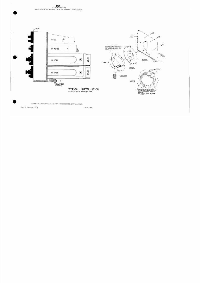
8/9/2019 KX 170A - Maintenance Manual Honeywell
http://slidepdf.com/reader/full/kx-170a-maintenance-manual-honeywell 380/586
KIN
KX 170B
T;
KX 175B
NAVIGATION RECEIVER/COMMUNICATIONS TRANSCEIVER
, PANEL
KAl6 RAM AIR KIT
(150-0083-00)
TYPICAL INSTALLATION
KAI6-KPN(071-4001-00) AND DIFFUSER STACK
FIGURE 2-5B KR 16 RAM AIR KIT AND DIFFUSER INSTALLATION
Rev. 1, January, 1976
Page 2-8B
VIEW
AIRCRAFT
SKIN -
OVER MANIFOL
IS POSITIONEN
D E S HO WN T H
NTED 160° THA
LWATER PROOF UNT IN THIS AREA
INCLUDING ENDS OF MOUNTNG SCREWS
WITH A ZINC CHROMATE SEALER,OR
EPUIVALENT.
( UNITVl~wS$JN TURNED IBO- FROM

8/9/2019 KX 170A - Maintenance Manual Honeywell
http://slidepdf.com/reader/full/kx-170a-maintenance-manual-honeywell 381/586
KiNG
r
-1
r
----
I
YPW)moa
I
I rtt
r
----
yzuocuo
r
FIGURE 2-6 TSO’D SILVER CRO WN SYSTEM INTERCONNECT
(DWG. NO. 155-1088-00 R-6 )
Page 2-9

8/9/2019 KX 170A - Maintenance Manual Honeywell
http://slidepdf.com/reader/full/kx-170a-maintenance-manual-honeywell 382/586
KlNG
KX 170B/KX 175B
NAVIGATION RECEIVER /
COMMUNICATIONS TRANSCEIVER
r
---
--pclDm
XX
1
I
I
r
---
X2"mole
r-----
a-
moa
\
)u3-a
1
I
I
FIGURE 2-7
KN 73/~~ 77 INTERCONNECT
(DWG. NO. 155-1117-00 R-3 )
Page 2-11
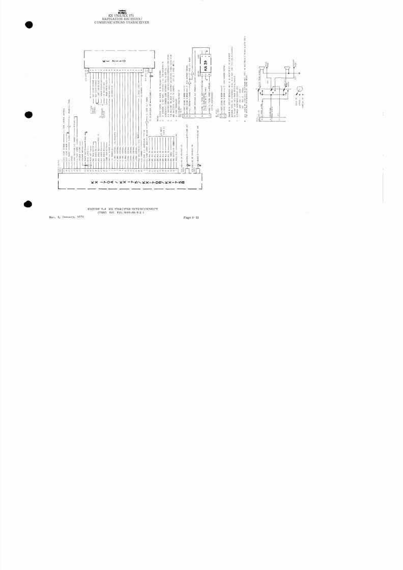
8/9/2019 KX 170A - Maintenance Manual Honeywell
http://slidepdf.com/reader/full/kx-170a-maintenance-manual-honeywell 383/586
KlNG
KX 170A/KX 175
NAVIGATION RECEIVER /
COMMUNICATIONS TRANSCEIVER
r
- -- - -
1
uN---o
I
FIGURE 2-8 KX 170B / 175B INTERCONNECT
(DWG. NO. 155-1089-00 R-5 )
Rev. 1, January, 1976
Page 2-13

8/9/2019 KX 170A - Maintenance Manual Honeywell
http://slidepdf.com/reader/full/kx-170a-maintenance-manual-honeywell 384/586
KING
r
I
I
--
1
I .
YZ (00
I
”
r-
--
r;
E8
1
c g 1.
YU NO--o
I
XX
-boa\Yx-born
EL
FIGURE 2-9
NON-TSO’D SILVER CROWN SYSTEM INTERCONNECT
(DWG. NO. 155-1090-00 R-8)
Page 2-15

8/9/2019 KX 170A - Maintenance Manual Honeywell
http://slidepdf.com/reader/full/kx-170a-maintenance-manual-honeywell 385/586
KING
r
---
4
--
“1 I
1
x- N--M
I
I
YX
CCIE
--Ice N
I-
a 5”
I
--------------Y
I
FIGURE 2-10 NOT TSO’S DUAL SILVER CROWN SYSTEM INTERCONNECT DIAGRAM
(DWG. NO. 155-1128-00 R-5)
Rev. 1, January 1976
Page 2-17

8/9/2019 KX 170A - Maintenance Manual Honeywell
http://slidepdf.com/reader/full/kx-170a-maintenance-manual-honeywell 386/586
r
I I I I I I I
\I
I I I I I I I I I 1 I
I I I I I I I I I I I I I I I II I I I II I
FIGURE 2-11
KX
17OA/175/17OB/175B/KI
214 INTERCONNECT
DIAGRAM
(DWG. NO. 155-1129-00 R-4)
Rev. 1,
January, 1976
Page 2-19

8/9/2019 KX 170A - Maintenance Manual Honeywell
http://slidepdf.com/reader/full/kx-170a-maintenance-manual-honeywell 387/586
KlNG
KX 170B/KX 175B
NAVIGATION RECEIVER /
COMMUNICATIONS TRANSCEIVER
SECTIONII
OPERATION
3.1 GENERAL
All controls required to operate the KX 170B/KX 175B are located on the unit front panel.
3.2 KX170B/KX175B NAVKOMM CONTROLS
3.2.1 COMM ON-OFF TEST CONTROL
The ON-OFF-TEST control is located directly above the COMM channel selector.
Power is
supplied to the COMM when this control is either in the ON or TEST position.
The TEST position
is used to defeat the COMM automatic squelch for both test purposes and listening to extremely
weak signals.
3.2.2 COMM VOLUME CONTROL
The Volume (VOL) control, located on the lower left side of the KX 170B/KX 175B is used to
adjust the transceiver audio volume. The KX 170B/KX 175B system power ON/OFF switch is
independent of this control, allowing the COMM volume to remain at a desired preset level.
3.2.3 COMM FREQUENCY SELECTOR
The two concentric knobs under the COMM frequency window are used to dial COMM frequencies.
The larger knob selects MHz and the smaller knob selects kHz. The transceiver is inoperable
in the two unused MHz positions between 118MHz and 135MHz.
Clockwise rotation selects higher
frequencies.
The dial mechanism has no stops, permitting continuous rotation.
3.2.4 NAV OFF-VOICE-IDENT CONTROL
The OFF-VOICE-IDENT control is located directly above the NAV channel selector.
Power is
supplied to the NAV when this control is either in VOICE or IDENT position.
NAV operation is
independent of COMM.
With the switch on IDENT, the ground station voice and identification
tone are coupled to the aircraft speaker and/or headphone circuitry.
With the switch on VOICE
the identification tone is eliminated, permitting the pilot to monitor the VOR ground station for
voice transmissions without receiving the VOR ident tone.
3.2.5 NAV VOLUME CONTROL
The navigation receiver volume (VOL) control, on the right side of the KX 17OB/KX 175B is used
to control the level of the audio and/or identification tone output from the navigation receiver.
This control is also independent of the system power switch allowing the NAV volume to remain
at a desired preset level.
3.2.6 NAV FREQUENCY SELECTOR CONTROLS
The two concentric knobs under the NAV frequency window are used to dial NAV frequencies.
The larger knob selects MHz and the smaller knob kHz.
Clockwise rotation selects higher fre-
quencies.
Remote DME, Glideslope, and ILS channeling are also performed by this control.
Page 3-l
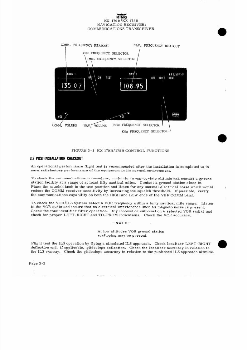
8/9/2019 KX 170A - Maintenance Manual Honeywell
http://slidepdf.com/reader/full/kx-170a-maintenance-manual-honeywell 388/586
KlNG
KX 170B/KX 175B
NAVIGATION RECEIVER /
COMMUNICATIONS TRANSCEIVER
COP. FREQUENCY READOUT
NAV. FREQUENCY READOUT
KHz FREQUENCY SELECTOR
\
MHz FREQUENCY SELECTOR
\
cod VOLUME
NAV,IvoLUME
MHz FREQUENCY SELECTOR
KHz FREQUENCY
FIGURE 3-1 KX 170B/175B CONTROL FUNCTIONS
3.3 POST-INSTALLATIONHECKOUT
An operational performance flight test is recommended after the installation is completed to in-
sure satisfactory performance of the equipment in its normal environment.
To check the communications transceiver,
maintain an appropriate altitude and contact a ground
station facility at a range of at least fifty nautical miles.
Contact a ground station close in.
Place the squelch knob in the test position and listen for any unusual electrical noise which would
reduce the COMM receiver sensitivity by increasing the squelch threshold. If possible, verify
the communications capability on both the HIGH and LOW ends of the VHF COMM band.
To check the VOR/ILS System select a VOR frequency within a forty nautical mile range. Listen
to the VOR audio and insure that no electrical interference such as magneto noise is present.
Check the tone identifier filter operation. Fly inbound or outbound on a selected VOR radial and
check for proper LEFT-RIGHT and TO-FROM indications.
Check the VOR accuracy.
-NOTE-
At low altitudes VOR ground station
scalloping may be present.
Flight test the ILS operation by flying a simulated ILS approach. Check localizer LEFT-RIGHT
deflection and, if applicable, glideslope deflection.
Check the localizer accuracy in relation to
the ILS runway. Check the glideslope accuracy in relation to the published ILS approach altitude.
Page 3-2

8/9/2019 KX 170A - Maintenance Manual Honeywell
http://slidepdf.com/reader/full/kx-170a-maintenance-manual-honeywell 389/586
,’
-
KlNG
KA 47
DME CODE CONVERTER
SECTIONV
KA47
4.1 GENERAL
The purpose of the King KA 47 is to convert the King KN 65 shift code obtained from the King
KX 170A/175/KX 170B/KX 175B to the standard ARINC 2 out of 5 DME code used in the King
KDM 700A. It is designed to be mounted next to the remote mounted DME equipment, and pin A
from 5301 should be grounded at the same point as the DME ground. The power requirement is
either 13. 75VDC or 27. 5VDC at 225 ma.
Standard digital troubleshooting techniques may be used in troubleshooting the King KA 47.
Page 4-l

8/9/2019 KX 170A - Maintenance Manual Honeywell
http://slidepdf.com/reader/full/kx-170a-maintenance-manual-honeywell 390/586
I
4 200
(IO 666)
4 620 MAX.
(11.734)
1
KlNG
KA 47
DME CODE CONVERTER
49OOMAx ,
(12 625)
C.G.
-- -
-f
2.465 REF.
- (6.261)
.16OiM)5 w--j
NOTE:
I. DIMENSIONS IN PARENTHESES ARE IN CENTIMETERS
2 WEIGHT: 0.6 LBS.
FIGURE 4 - 1 OUTLINE AND MOUNTING DIAGRAM
(DWG. NO. 155-5082-00 R-O)
Page 4-2

8/9/2019 KX 170A - Maintenance Manual Honeywell
http://slidepdf.com/reader/full/kx-170a-maintenance-manual-honeywell 391/586
KlNG
KA 47
DME CODE CONVERTER
1Yx-~om
L--
x--ha
z
J
r-
------
I
xnl-8)pco
YPI booa
FICWRE
-2 KA 47 INTERCONNECT DIAGRAM
(DWG. NO. 155-1102-00 R-2)
Page 4 -3

8/9/2019 KX 170A - Maintenance Manual Honeywell
http://slidepdf.com/reader/full/kx-170a-maintenance-manual-honeywell 392/586
MAINTENANCE/OVERHAUL
MANUAL
KX 17OB/KX758
NAV/COMM
TRANSCEIVER
KIN-G RADIO CORPORATION,
400
NORTH ROGERS ROAD
OLATHE, KANSAS, U.S.A.

8/9/2019 KX 170A - Maintenance Manual Honeywell
http://slidepdf.com/reader/full/kx-170a-maintenance-manual-honeywell 393/586
Paragraph
4. 1
4. 2
4. 2. 1
4. 2. 2
4. 3
4.3. 1
4.3.2
4.4
5. 2
Alignment & Test Procedure
5-7
5.2. 1
Nav SMO Alignment & Test
5-7
5.2.2 Comm SMO Alignment & Test 5-8
5.2.3
Nav/Comm Receiver Preliminary Alignment Test
5- 10
5.2.4
Nav Receiver Alignment
5-11
5.2.5
Comm Receiver Alignment
5- 13
5. 2.6
Transmitter Alignment
5-14
5.2.7
.‘Notes: Standard Signal
5-15
5. 2.8
KX 170B /Kx 175B Final Test Data
5-20
5. 3
5. 4
5.4. 1
5.4.2
5.4.3
5.4.4
5.4. 5
5.4.6
5.4.7
5. 4.8
5.4.9
5.4. 10
5.4.11
5.4.12
KlNG
JSX 17OB/KX 175B
NAVIGATION RECEIVER/
COMMUNICATIONS TRANSCEIVER
TABLEOFCONTENTS
SECTIONV THEORYFOPERATION
General
4-l
Frequency Synthesizers
4-l
SMO Block Diagram
4-l
SMO Circuit Theory
4-6
COMM Transceiver
Block Diagram Theroy
COMM Transceiver Circuit Theory
4-9
4-9
4-10
NAV Receiver
4-11
SECTION MAINTENANCE
General Maintenance
Visual Inspection
Cleaning
Semiconductor Replacement
Semiconductor Replacement Maintenance
Semiconductor Replacement Voltage & Resistance Measurement
Digital Logic Functions
5-l
5-l
5-l
5-l
5-l
5-2
5-5
Troubleshooting The KX 17OB/KX 175B
5-27
Troubleshooting The Nav SMO
5-32
Preliminary Evaluation
5-32
Nav SMO Diagnostic Procedure
5-32
Programmable Divider 5-34
Phase & Freq. Comparator
5-35
Low Reference Oscillator
5-36
Voltage Controlled Oscillator
5-36
VCO Low Pass Filter
5-36
25KHz Voltage Translator
5-36
Receiver Buffer
5-36
VCO Buffer
5-37
High Reference Oscillator
5-37
Implicit Divide By 2 Circuit
5-37
Page

8/9/2019 KX 170A - Maintenance Manual Honeywell
http://slidepdf.com/reader/full/kx-170a-maintenance-manual-honeywell 394/586
KlNG
KX 170B/KX 175B
NAVIGATION,RECEIVER/
COMMUNICATIONS TRANSCEIVER
TABLEOFCONTENTS
Paragraph
Page
5.4. 13 2nd Mixer
5-37
5.4. 14
Mixer Low Pass Filter
5-37
5.4. 15
Squaring Amplifier
5-37
5. 5
Troubleshooting The Comm SMO
5-37
5. 5. 1
Preliminary Evaluation
5-39
5. 5.2
Comm SMO Diagnostic Procedure
5-39
5. 5.3
Programmable Divider
5-44
5. 5.4
Phase & Freq. Comparator
5-46
5. 5. 5
Voltage Controlled Oscillator
5-46
5. 5.6
VCO Low Pass Filter
5-47
5. 5.7
25KHZ Voltage Translator
5-48
5. 5.8 Receiver Buffer
5-48
5. 5.9
Transmit Buffer/TX Enable Switch/Out Of Lock TX Disable
5-48
5. 5. 10
High Reference Oscillator
5-48
5. 5. 11 Implicit Divide By 2 Circuit
5-49
5. 5. 12
2nd Mixer
5-49
5. 5. 13 Mixer Low Pass Filter
5-49
5. 5. 14
Squaring Amplifier
5-49
5. 6
Troubleshooting The Nav Receiver
5-59
5. 7
Troubleshooting The Comm Receiver
5. 8
Troubleshooting The Audio Amplifier
5-59
5-59
5. 9
Troubleshooting The Transmitter
5-59
5. 10 Troubleshooting The Regulators
5-59
5. 10. 1
Comm 8. 5 Volt Regulator
5-59
5. 10. 2 8. 5 Volt Nav Regulator
5-59
5. 11 Troubleshooting The KA 39 Voltage Regulator
5-59
SECTIONI ILLUSTRATEDARTS IST
::
3.
4.
5.
6.
7.
.8,.
9.
10.
11.
12.
Final Assembly
Front Plate Sub-Assembly
Front Plate Sub-Assembly
Switching Head Sub-Assembly
Switch Wafer Assemblies
NAV SMO Board Sub-Assembly
NAV SMO Sub-Assembly
COMM SMO Board Sub-Assembly
COMM SMO Sub-Assembly
NAV/COMM Board Sub-Assembly
Transmitter Board Sub-Assembly
Rear Plate Sub-Assembly
6-l
6-4
6-9A
6-10
6-14A
6-23
6-29
6-32
6-39
6-42
6-51
6-54
SECTION MAINTENANCE
ii
8/9/2019 KX 170A - Maintenance Manual Honeywell
http://slidepdf.com/reader/full/kx-170a-maintenance-manual-honeywell 395/586
Paragraph
13.
14.
15.
Figure
4-l KX 170B/KX 175B Simplified SMO Block Diagram
4-2
‘4-2 Typical Loop Transfer Functions
4-3
5-l
5-2
5-3
5-4
5-5
5-6
5-7
5-8
5-9
5-10
5-11
5-12
5-13
5-14
5-15
5-16
5-17
5-18
5-19
5-20
5-21
5-22
5-23
5-24
5-25
5-26
5-26A
5-27
5-28
5-28A
5-29
5-30
5-31
5-32
KX I 70B/KX 175B
KlNG
I(x 170B/KX 175B
NAVIGATION RECEIVER/
COMMUNICATIONS TRANSCEIVER
TABLEOFCONTENTS
SECTIONI ILLUSTRATEDARTS IST
Page
Audio Drive Board Sub-Assembly 6-57
Rear Divider Sub-Assembly
6-60
Connector and Cable Sub-Assembly 6-65
LISTOF ILLUSTRATIONS
Basic Logic Functions
Reset and Preset Counters
Test Circuit
Receiver Alignment Loading Points
Microphone Gain Adjust Detector W aveforms
Dectector Schematic Diagram
RF Attenuator Schematic Diagram
KX 170B/KX 175B Bench Test Setup
Troubleshooting Flow Chart
Programmable Divider Output
Voltage Translator
Programmable Divider
Low Reference Oscillator Output
Mixer Output
Squaring Amplifier Output
Programmable Divider Output
Voltage Translator
Programmable Divider
Low Pass Filter
NAV Programmable Divider Timing Diagram
COMM Programmable Divider Timing Diagram
COMM Programmable Divider Timing Diagram
Freq. and Phase Comparator Timing Diagram
NAV Block Diagram
COMM Block Diagram
NAV /COMM Receiver Schematic and Assembly
NAV /COMM Receiver Schematic and Assembly
NAV SMO Schematic and Assembly
Audio Assembly
Transmitter and Audio Schematic and Assembly
COMM SMO Schematic and Assembly
Switch Wiring Diagram/Voltage Regulator
Switching Matrix/Switch Wiring/Voltage Regulator
KA 39 Voltage Schematic and Assembly
5-6
5-6
5-15
5- 16
5- 17
5-18
5-18
5-19
5-25
5-33
5-33
5-35
5-40
5-41
5-42
5-43
5-44
5-45
5-47
5-51
5-53
5-55
5-57
5-60
5-61
5-63
5-63A
5-65
j-67
5-67A
5-69
5-71
5-73
5-75
111

8/9/2019 KX 170A - Maintenance Manual Honeywell
http://slidepdf.com/reader/full/kx-170a-maintenance-manual-honeywell 396/586
Figure
LISTOF ILLUSTRATIONS
6-l
6-1A
6-2
6-2A
6-3A
6-3b
6-3C
6-4
6 -4A
6-5
6-5A
6-6
6-7
6-8
6-9
Final Assembly (KX
Final Assembly (KX
Final Assembly (KY
Final Assembly (KY
Front Plate Assemb
Front Plate Assemb
Front Plate Assemb
170B/KX 1758)
170B/KX 175B)
195B
195B
ly (KX 170B/KX 175B/KY 1958)
ly (KX 17OB/KX 175B/KY
1958)
ly (KX 170B/KX 175B/KI 195B)
Switching Head Sub-Assembly (KX 170B/KX 175B)
Switching Head Sub-Assembly (KX 170B/KX 175B)
Switching Head Sub-Assembly (KY 195B)
Switching Head Sub-Assembly (KY 195B)
NAV SMO Sub-Assembly
COMM SMO Sub-Assembly
Rear Plate Sub-Assembly
Rear Divider Sub-Assembly
TABLES
No.
4-l
T-R Switching Requirements
4-2
Frequencies Appearing In The Kx 170B/ KX 175B
4-3
Selected Frequency Division
5-l
5-2
5-3
5-4
5-5
5-6
5-7
5-8
5-9
5-10
5-11
NAV Channel-SMO Frequency-VCO Tuning Voltage
5-8
COMM Channel-Receive SMO Frequency-VCO Tuning Voltage
5-9
COMM Channel-Receive SMO Frequency-Tuning Voltage
5-10
NA\i Channel-SMO Frequency-Receiver Tuning Voltage 5-11
NAV SMO Trouble Chart
5-28
COMM SMO Trouble Chart
5-29
In Kx 170A/ KX 175 Maintenance Manual
COMM SMO Synthesizer Frequencies
5-38
High Feference Osc. Troubleshooting Table
5-48
KX 170B/KX 175B
NAVLGATION RECEIVER/
COMMUNICATIONS TRANSCEIVER
TABLE FCONTENTS
Page
6-3
6-3A
6-38
6-3C
6-9
6-90
6-9E
6-15
6-17
6-19
6-21
6-31
6-41
6-56A
6-63
4-4
4-5
4-7
l
iv

8/9/2019 KX 170A - Maintenance Manual Honeywell
http://slidepdf.com/reader/full/kx-170a-maintenance-manual-honeywell 397/586
KlNG
KX l’IOB/KX 175B
NAVIGATION RECEIVER/
COL IMUNICATIONS TRANSCEIVER
The information in thts maintenance manual does not profess to include all the details of design,
production, or variations of the equipment,
or to cover all the possible contingencies which may
arise during operation,
installation, or maintenance.
Should special problems arise or further
information be desired, please contact the KING Customer Service Department.
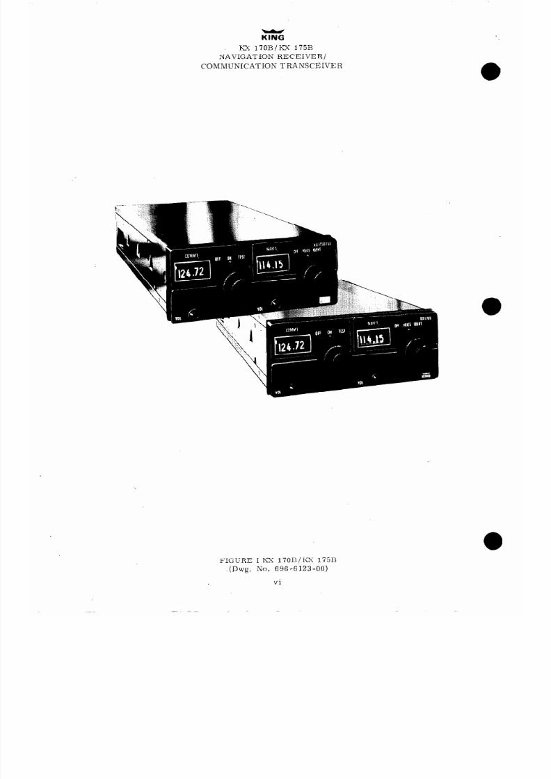
8/9/2019 KX 170A - Maintenance Manual Honeywell
http://slidepdf.com/reader/full/kx-170a-maintenance-manual-honeywell 398/586
KX 170B/KX 175B
NAVIGATION RECEIVER/
COMMUNICATION TRANSCEIVER
FIGURE I KX 170B/KX 175B
.(Dwg. No. 696-6123-00)
vi

8/9/2019 KX 170A - Maintenance Manual Honeywell
http://slidepdf.com/reader/full/kx-170a-maintenance-manual-honeywell 399/586
KlNG
KX 170B/KX 175B
NAVIGATION RECEIVER /
COMMUNICATIONS TRANSCEIVER
SECTIONV
THEORY FOPERATION
4. 1 General
The KX 170B/KX 175B unit incorporates a 200 channel navigation receiver, a 720 channel com-
munications transceiver and a 5 watt audio system.
For discussion purposes, the KX 170B/KX 175B system is split into subsystems and treated on
the basis of block diagram theory and detailed circuit theory.
Subsystems are defined as Fre-
quency Synthesizers (COMM and NAV), COMM Transceiver and NAV Receiver.
4.2 Frequency Synthesizers
4.2.1
SMO BLOCK DIAGRAM
4.2. 1. 1
Simplified Block Diagram.
The KX 1’70B/KX 175B uses a stabilized maste r oscillator (SMO) for frequency generation. A
feedback loop is used to slave a voltage controlled oscillator (VCO) to the selected multiple fre-
quency of a crystal controlled reference oscillator. The simplified block diagram of Figure 4-l
illustrates the principle of operation of the COMM SMO and NAV SMO.
The VCO output frequency is divided by two,
mixed with the High Frequency Crystal Oscillator,
divided by N, and compared in frequency and phase with the Low Frequency Crystal Oscillator.
The filtered error signal b iases the VCO. The error signal is a high voltage when the VCO
frequency is low and a low voltage when the VCO frequency is above the desired frequency.
According to the VCO transfer function (Figure 4-2b) this error signal drives the VCO toward the
selected frequency.
When the VCO gets near the desired frequency, the loop captures the VCO
and pulls it into phase lock (fVC0 =f selected).
In this condition the loop establishes an error
signal that is a 25KHz square wave. The low pass filter recovers the dc component and biases
the VCO to maintain the selected output frequency. The square wave duty factor, and thus the
filtered D-C VCO bias voltage, varies according to the selected VCO frequency. Transfer func-
tions of the various blocks are illustrated in Figure 4-2.
4.2. 1.2
NAV SMO Block Diagram.
The NAV SMO is a 200 channel frequency synthesizer covering the band from 92.8125-102.7625MHz
in 50KHz steps.
The block d iagram is the red shaded portion of Figure 5-24.
The basic
frequencies appearing in the NAV SMO are tabulated in Table 4-2 and also appear on the block
diagram.
The VCO converts a dc bias voltage to a VHF frequency.
The buffer amplifiers isolate the VCO
from reverse conducted electrical interference signals and provide 1Omw output levels for mixer
injection. The Implicit Divide by Two circuit halves the VCO frequency.
A mixer is used to
heterodyne the halved VCO frequency and the High Frequency Reference Oscillator.
The Mixer
Low Pass Filter passes the difference frequency and filters any spurious mixer products.
In the
Squaring Amplifier the analog difference frequency is amplified and clipped to provide a 4. 5V
square wave. The Programmable Divider generates one output pulse for every N input pulses.
Selection of the divide ratio, N, is determined by the wafer switch coding.
The 4OOKFz Reference
Oscillator is divided by 16 in the Phase and Frequency Comparator block to obtain a 25KFz refer-
ence.
This block also compares the Programmable Counter output in frequency and phase with
the 25KHz reference frequency and generates an appropriate feedback signal to slew the loop until
February, 1973
Page 4-1
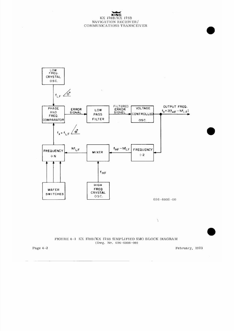
8/9/2019 KX 170A - Maintenance Manual Honeywell
http://slidepdf.com/reader/full/kx-170a-maintenance-manual-honeywell 400/586
KlNG
KX 170B/KX 175B
NAVIGATION RECEIVER /
COMMUNICATIONS TRANSCEIVER
fLF
L
0
+
PHASE
AND
FREQ.
ERROR
SIGNAL )
LOW
PASS
FILTERED
ERROR
SIGNEL
1 FILTER 1
FREQUENCY NfLF fHF-NfLF FREQUENCY
MIXER
4
e
+N
,2
A 4 b1
fHF
HIGH
1
REO
CRYSTAL
osc.
VOLTAGE
CONTROLLE
osc.
t
OUTPUT FREQ.
,fo= 2(fHF-NfLF;
696-6008 -00
FIGURE 4-l KX 170B/KX 175B SIMPLIFIED SMO BLOCK DIAGRAM
(Dwg. Nc. 696 -6008 -00)
Page 4-2
February, 1973

8/9/2019 KX 170A - Maintenance Manual Honeywell
http://slidepdf.com/reader/full/kx-170a-maintenance-manual-honeywell 401/586
KI G
r
X 170B KX 175B
NAVIGATION. RECEIVER /
COMMUNICATIONS TRANSCEIVER
February, 1973
A) TYPICAL LOW PASS FILTER FREQ. RESPONSE
IO’KHZ
25’twz
FREQUENCY
El TYPICAL VCO TRANSFER FUNCTION
DC’ BIAS VOLTA&E
C) PHASE AND FREQ. COMPARATOR
t
fDESIRED FREQ.
FIGURE 4-2 TYPICAL LOOP TRANSFER FUNCTIONS
(Dwg. No. 696-6108-00)
Page 4-3

8/9/2019 KX 170A - Maintenance Manual Honeywell
http://slidepdf.com/reader/full/kx-170a-maintenance-manual-honeywell 402/586

8/9/2019 KX 170A - Maintenance Manual Honeywell
http://slidepdf.com/reader/full/kx-170a-maintenance-manual-honeywell 403/586
KlNG
KX 17OB/KX 175B
NAVIGATION RECEIVER /
COMMUNICATIONS TRANSCEIVER
Selected Channel
(50KHz steps NAV)
(25KHz steps COMM
VCO Frequency
(50KHz steps NAV)
(25KHz steps COM)
Implicit + 2 Freq.
(25KHz steps NAV)
(12. 5KHz steps
COM)
H. F. REF Freq.
Mix Output Freq.
Divide Ratio
L. F. REF Freq.
Approx. VCO Bias
Approx. Receiver
tuning Voltage.
1st I. F. Freq.
2nd I. F. Freq.
2nd L. 0. Freq.
NAV
108.00 - 117.95MHz
92.8 125 - 102.7625MHz
118.00 - 126.975RMH2
127.00 - 135.975T
127.000 - 135. 975MHT
46.40625 - 51.38 125MHz
63. 500 - 67.9875MHz
53.93125MHz
71.0375MHz
7. 525 - 2. 550MHz
301 - 102
7. 5375 - 3.050MHz
301.5 - 122
400KHz = 25~~~
16
400KHz = 25~~~
16
2.95
- 7.20 Volts
2.95 - 7.20 Volts
15.1875MHz
2. 50
- 7.00 Volts
2.95 - 7.80
9.ooooMHz
1. 1857MHz
861.2500KHz
14.00 18 MHz
8.13875MHz
F
COMM
I
SMO HIGH BAND
I
MO LOW BAND
I
--7
I
127.00 - 135.975RMHz
118.00 - 126.975T
118.000 - 126. 975MI
I
IZ
59.000 - 63.4875MH;
66. 5375MHz
7. 5375 - 3.050MHz
301. 5 - 122
400KHz
=25KHz
16
2.50 - 7.00 Volts
TABLE 4-2 FREQUENCIES APPEARING IN THE KX 170B/KX 175B
The phase locked loop synthesizes 360 channels in each 9MHz band and is switched between high
and low bands with the High Reference Oscillator crystals and the VCO band switch.
This system
provides 720 channels with a 180 digit counter and fast T-R transitions without requiring special
coding of the Programmable Divider. Note that the receiver uses a combination of high and low
side injection and that the first I-F frequency is restricted to 9. OMHz.
The Out of Lock Disable block turns off the receiver buffer and transmitter buffer when the SMO
is out of lock.
The VCO is disabled in the two unused MHz positions of the frequency selector.
February, 1973
Page 4-5

8/9/2019 KX 170A - Maintenance Manual Honeywell
http://slidepdf.com/reader/full/kx-170a-maintenance-manual-honeywell 404/586
KlNG
KX 170B/KX 175B
NAVIGATION RECEIVER /
COMMUNICATIONS TRANSCEIVER
Formulas for the synthesized frequencies are:
(Low band)
fvco
=2 (66. 5375 - .025N) MHz
(High Band) fvco =2 (71.0375 - .025N) MHz
where N is any selected number from 122 to 30 1. 5.
4.2.2 SMO Circuit Theory
4.2.2. 1 Balanced Mixer - NAV (COMM)
T206, T207, CR207 thru CR210 (T304, T306, CR309 thru CR310) and associated components form
the balanced mixer. The balanced mixer configuration was chosen to minimize spurious genera-
tion and to provide isolation between the digital circuitry,
the VCO, and the high reference oscilla-
tor.
4.2.2. :
Mixer Low Pass Filter - NAV (COMM)
C239, C240, and L204 (C375, C376, and L305) form the mixer low pass filter, which is used to
remove high frequency mixer products.
4.2.2.3 Squaring Amplifier
Q206 and Q209 (Q312, and Q313) are used in a complementary configuration to provide wide band
amplification and clipping.
The output waveform is a 4 volt square wave.
4.2.2.4 400KHz Reference Oscillator - NAV (COMM)
Q210, Q211, Y202 (Q315, 316, Y303 - KX 175B Only) and associated components form the low
frequency reference oscillator.
The 400KHz reference signal is applied to both the NAV and
COMM phase and frequency discriminator circuits.
4.2.2.5
Programmable Divider - NAV
The KX 170B/KX 1758 N-4V ProgrammableDivider is identical to the KX 170A/KX 175 NAV
Programmable Divider.
Refer to the KX 175 Maintenance Manual Section IV for NAV Program-
mable Divider Circuit Theory, and Figure
5-27 of this section for the NAV SMO schematic and
component placement.
4.2. 2. 6
Programmable Divider (COMM Figure 5-29)
The programmable divider consists of an input inhibit circuit (25KHz Section, 1309 and 1303C)
and three synchronous,
cascaded counter blocks; divide by 2 (50KHz Section, 1301), divide by 10
(1OOKHz Section, 1303D, 1304B, and 1306), and divide by 15 (MHz Section, 1302, 1303A, and
1304A).
The divide by 2, 10 and 15 provides 300 counter states (2x10~15). The input inhibit
provides one additional state by inhibiting the input for one pulse.
Since one input pulse is used to
strobe preset information into the registers,
the counter has a total of 302 available states
(2x10~15) +l+l. Each input pulse steps the counter to the next state.
To divide by N, the counter
is preset N states away from the load state.
After N input pulses, the load state is reached and
an output pulse is generated.
The counter is preset and the cycle is repeated. To divide by
N f. 5, the sequence is the same as that above except that for every other output pulse, the input
Page 4-6
February, 1973

8/9/2019 KX 170A - Maintenance Manual Honeywell
http://slidepdf.com/reader/full/kx-170a-maintenance-manual-honeywell 405/586
KlNG
KX 170B/KX 175B
NAVIGATION RECEIVER/
COMMUNICATIONS TRANSCEIVER
to the counter is inhibited for one input pulse. That is, the counter will alternately divide by
N and N+l, the average result is N+. 5.
The division ratios for the COMM SMO are 30 1. 5 to
122.
The chart relating preset state and selected channel for the COMM SMO appears in Table
4-3.
NI
MHz
Preset
MO Ml M2 M3
N2
KHz
Preset
KHz
Koo K. Kl K2 K3 N3 Preset Kol
280
118, 127 1 1 0 1
260
119, 128
1 1 1 0
240
120,129
0 1 1 1
220
121, 130
0 0 1 1
200
122, 131
0 0 0 1
180
123, 132
0 0 0 0
160
124, 133
1 0 0 0
140
125, 134
0 1 0 0
120 126. 135 1 0 1 0
100 0 1 0 1
80 0 0 1 0
60
1 0 0 1
40 1 1 0 0
20 0
1 1 0
Load State
1 0 1 1
20
19
18
17
16
15
14
13
12
11
10
9
8
7
6
5
4
3
2
.025
.075
125
: 175
.225
. 275
. 325
375
: 425
. 475
. 525
. 575
. 625
. 675
.725
* 775
.825
.875
.925
1
0
1
0
1
0
1
0
1
0
1
0
1
0
1
0
1
0
1
l(Load. 975 0
State)
1 1 1 0
0.5 -.025 1
1 1 1 0
0.0 - 0.0 0
0 1 1 1
0 1 1 1
0 0 1 1
0 0 1 1
0 0 0 1
0 0 0 1
0 0 0 0
0 0 0 0
1 0 0 0
1 0 0 0
1 1 0 0
1 1 0 0
0 1 1 0
0 1 1 0
1 0 1 1
1 0 1 1
1 1 0 1
1 1 0 1
SELECTED FREQUENCY DIVISION(N) =Nl+N2+N3+1
TABLE 4-3
Figure 5-29 shows the integrated circuits as they appear on the COMM SMO Printed Circuit
Board and the COMM SMO schematic. The counter timing diagram appears in figures 5-2 1 and
5-22.
With the KHz knob set to the .X25 or . X75 positions (Kol =O, 1303 Pm 8 =l), the operation of the
KHz sections of the COMM and NAV Programmable Dividers are identical.
130 1B presets 130 1A
when the counter reaches the load state.
During normal operation the J inputs, pins 13 and 14
are high, the I? input, pin 12 is high, and 1301B remains with Q high regardless of the Koo input
to pin 11. When the load state is reached, pin 6 of 1304 goes negative.
If the preset input, 1301
pin 11 is high, the preset clock-pulse will drive Q of 1301B low.
If the preset input, pin 11, has
been low the next pulse would leave Q of 1301B high.
If pin 10 (Q) remains high then the K input
to 1301A remains high and 1301A continues to act as a toggle flip-flop.
However, if pin 10 goes
low, 13OlA automatically shifts a high state to the Q output at pin 6.
The divide by 2 function and
the preset waveform are illustrated in Figure 5-21 and 5-22.
With the KHz knob set to the . X00 or .X50 positions (K,l = l), the operation of the divider is as
follows.
1309B divides the output of the programmable divider by 2.
(pin 9) goes to a “O”, 1309A is reset to a
When 130 1B Q output
=“l” (pin 6) and 1303 pin 8 remains a “1”.
Operation
of the divider is as described above.
When the next divider output pulse occurs, 1309B, Q (pin 9)
output is clocked to a “I”, 1309A, Qremains at a
“1” and 1303 pin 8 goes to a “0” inhibiting 1301.
(J and K inputs = “0’: therefore 1301 will not change state). When the next input clock pulse
February, 1973
Page 4-7

8/9/2019 KX 170A - Maintenance Manual Honeywell
http://slidepdf.com/reader/full/kx-170a-maintenance-manual-honeywell 406/586
KlNG
KX l’IOB/KX 175B
NAVIGATION RECEIVER/
COMMUNICATIONS TRANSCEIVER
occurs, 1309A is toggled to Q = “0” and 1303, pin 8 goes to a “l”, enabling 1301. The divider
l
now returns to normal operation and the cycle is repeated.
By inhibiting the divider for one clock
pulse every o ther time the XXX. 5 average division ratios are accomplished.
The 9300 is a synchronous, 4 flip-flop shift register. Serial entry is available through the J-K
inputs during positive clock transitions.
when simultaneouslv:
Parallel entry is through PO, Pl, P2, and P3 inputs
the Parallel Enable (PE) port is low and the clock pulse (Cp) makes a posi-
tive transition. Outputs QO, &I, Q2, Q3,Q3 and an asynchronous maste r reset (MR) are externally
available.
1303D and I3 06 (KHz 9300) are connected to provide a 10 state shift counter (1OOKHz portion of
divider). 1304B is used to monitor a of 1301A and QO, Ql and Q3 of 1306.
When the 4 inputs are
high, the output goes low.
The next clock pulse toggles 1301A causing the output of 1304B to go
high providing the clock pulse to 1302 (MHz 9300).
1304B provides 1 output pulse for every 20
input pulses to 130 1A. See Figures 5-21 and 5-22.
1302 (MHz 9300) is wired to provide a 15 state counter.
1304A monitors the inverted clock pulse
and QO, Q2, and Q3 of 1302. The counter load state occurs when all of these inputs are high. In
the load state 1304 pin 6 goes to a “O”,
providing a parallel enable to 1301, 1302, 1306, and 1309.
The next clock pulse transition strobes in the preset information.
4.2.2.7
Phase and Frequency Comparator - COMM (NAV)
1310, 1311, and 13 12 (1210, 12 11, 1212) form the phase and frequency comparator.
The schematic
and component placement is shown in figure 5-29 (5-27) and the timing diagram in figure 5-23.
The 400KHz low frequency reference oscillator is divided by 1310 (1210) to provide a 25KHz
reference.
1311 (1211) C and D form a set-reset flipflop. This flip flop is used to provide phase
comparison of the programmable counter output and the 25KHz reference signal.
When the
system is phase locked, 13 11 (12 1 )A and 13 12 (12 12) B form a pulse generator which triggers on
the positive going edge of the reference 25KHz signal to set the set-reset flip flop and I311 (1211) B
and I3 12 (12 12)A form a pulse generator which triggers on the positive going edge of the variable
divider output to reset the set-reset flip flop.
The output of the set-reset flip flop during phase
locked conditions is a square wave with a duty cycle proportional to the relative phase of the two
input s ignals.
When the system is out of lock, the programmable divider output frequency (13 12 pin 3 (12 12 pin 3)
will not equal 25KHz. If the frequency at 1312 (1212) pin 3 is greater than 25KHz, 1311 (1211) pin
11 will be low and the pulse width at 13 11 (12 11) pin 5 will vary.
If the frequency at 13 12 (12 12)
pin 3 is less than 25KHz, 13 11 (I2 11) pin 11 will be high and the pulse width at 13 11 (12 11) pin 1 will
vary.
The basic transfer function of the Phase and Frequency Comparator is illustrated in Figure 5-23.
If power is turned on or channels are changed the appropriate high or low voltage is generated to
sweep the VCO toward the selected channel frequency,
whereupon the VCO is captured by the
reference frequency with phase sensitive detector action.
4.2.2.8
Out of Lock TX Disable
When Q307 is biased off, the Transmit Buffer, Q306, and Receiver Buffer, Q303, are disabled.
During proper phase lock operation, the base of Q307 is high, saturating the transistor and
enabling the Transmit and Receive Buffers. If the loop fails to lock, either 1312 (1212) pin 8 or 6
will go high (See Figure 5-23) and Q318 will saturate, grounding the base of Q307. This inhibits
the Transmit and Receive Buffers.
Page 4-8
February, 1973

8/9/2019 KX 170A - Maintenance Manual Honeywell
http://slidepdf.com/reader/full/kx-170a-maintenance-manual-honeywell 407/586
KlNG
KX l’IOB/KX 175B
NAVIGATION RECEIVER/
COMMUNICATIONS TRANSCEIVER
4.2.2.9 Voltage Translation Circuit - COMM (NAV)
Q3 17 (Q2 12) and associated components amplify the output of the Phase and Frequency Compara-
tor to obtain the proper voltage for the VCO control.
4.2.2. 10 Low Pass Filter - COMM (NAV)
T307, T308 (T201, T208) and associated components form a 12. 5KHz (25KHz) low pass filterto
recover the DC component of the 25KHz square wave.
This DC voltage is the VCO control voltage.
R326, R327, and C347 (R208, R209, and C210) form a lag-lead network which provides loop
stability.
4.2.2. 11 Circuit Theory - SMO RF Circuits
Refer to KX 175 manual, paragraph 4.2.2.2 and figures 5-26 and 5-28 for VCO, Buffer Ampli-
fier, Implicit Divide by 2, and NAV High Frequency Oscillator Circuit Theory.
4.2.2. 12 COMM High Frequency Reference Oscillator
Q3 11, Y30 1, and Y302 form the COMM High Frequency Reference Oscillator.
Y30 1 (7 1.0375MHz)
and C334 are selected for the high SMO band (127.00 - 135.975MHz) and Y302 (66. 5375MHz) and
C332 are selected for the low SMO band (118.00 - 126.975MHz). See Table 4-2 for correspond-
ing transmit and receive frequencies.
4.3 Comm Transceiver
4.3.1 BLOCK DIAGRAM THEORY (Figure 5-25)
The KX 170B/KX 175B COMM receiver section is a dual conversion, superheterodyne receiver
with a 9. OMHz first I-F and a 861.25KHz second I-F frequency. 720 channels are synthesized at
the first mixer. Low side injection is used for channels 127.000 - 135. 975MHz and high side for
118.000 - 126.975MHz.
The received antenna signal is coupled to the preselector through a diode T/R switch.
A 2-pole,
varactor tuned, R-F filter couples the antenna to the R-F stage. A second varactor tuned filter
couples the amplified R-F signal to the 1st mixer and supplies additional image and l/2 I-F
spurious rejection. The amplified R-F signal is mixed with the synthesized injection frequency
in a balanced mixer.
A two pole (KX 170B) or 6 pole (KX 175B) crystal filter couples the differ-
ence frequency to the second mixer and provides image and l/2 I-F selectivity, The 8. 13875MHz
crystal controlled 2nd local oscillator develops injection for the 2nd mixer. The 2nd I-F contains
two integrated circuit (I-C) amplifiers with three double-tuned interstage networks for additional
receiver selectivity. An active detector/noise limiter provides audio gain, rate noise limiting,
and 90% AM clipping of noise spikes. A two stage AGC amplifier is used to AGC the R-F stage,
and the 1st I-C amplifier in the 2nd 1-F strin.
The receiver is approximately 6db into AGC with no input signal. This eliminates conventional
gainthreshold effects and establishes a constant “Signal plus noise” at the detector output. The
detector noise bandwidth is approximately 15KHz. A noise filter passes white noise containing
frequency components above 7KHz.
The filtered noise is amplified and used to operate a squelch
gate.
When detected white noise drops below a preset threshold, the squelch gate opens.
If a
detected audio tone falls within the filter passband, it is treated as noise and blocks the squelch.
A carrier squelch overcomes this problem by opening the squelch gate when the AGC exceeds a
February, 1973
Page 4-9

8/9/2019 KX 170A - Maintenance Manual Honeywell
http://slidepdf.com/reader/full/kx-170a-maintenance-manual-honeywell 408/586
2iK
KX l’IOB/KX 175B
NAVIGATION RECEIVER/
COMMUNICATIONS TRANSCEIVER
predetermined voltage. Receiver Audio passes through the volume control, an audio amplifier
and is coupled to the audio summing junction.
The summing junction accepts four auxilary audio inputs including NAV and Intercom Microphone.
A diode switch mutes the summing junction and connects the mike element to the audio power
amplifier during transmit.
Headphone/sidetone is capacitively coupled from the audio drive
amplifier to the phone jack and is still operable with shorted audio output or R-F power transis-
tors. The push-pull audio amplifier supplies 6 watts to the balanced primary of the output trans-
former. The secondary includes separate speaker and modulation windings.
The transmitter is a solid state, 4 stage, broadband, 30db gain, R-F power amplifier. Collector
modulation is applied to the driver and final stages.
The low pass filter provides harmonic
spurious rejection. COMM SMO band switching, speaker /modulator, headphone/sidetone and
antenna connections are controlled with a T/R relay,
R-F/audio circuitry,
A series regulator supplies 8. 5 volts to
and a zener regulator maintains 5. 0 volts to digital circuitry used in the
frequency synthesizers.
4.3.2 COMM TRANSCEIVER CIRCUIT THEORY
With the exception of the first I-F Filter,
Audio Filter, Summing Junction T/R Switch, Audio
Power Amplifier and Voltage Regulators,
the KX 170B/KX 175B is identical to theKX 170A/KX 175
Refer to paragraph 4. 3.2 of the KX 175 Maintenance Manual for COMM Transceiver Circuit
Theory not covered in this section.
4.3.2. 1
First I-F Filter (Figure 5-26)
The difference frequency (9MHz) is coupled through the crystal filter (FL403, KX 170B/FL405,
FL406, FL407, KX 175B) and applied to the base of the 2nd mixer, Q413.
Tuned circuits, T414
and T415 provide reactive tuning of the crystal filter.
4.3. 2.2 Summing Junction T/R Diode Switch (Figure 5-28)
Resistor R703.-707, R729 and R722 provide a summing junction.
In the receive condition, CR701
is reverse biased and CR702 is forward biased, passing audio to the audio pre-driver stage, Q701.
When the mike is keyed, the T/R relay grounds R721, which mutes CR702 audio and forward
biases CR70 1 applying mike audio to Q70 1.
4.3.2.3
Audio Power Amplifier (Figure 5-28)
Transistors Q70 l-706 are connected in a conventional audio power amplifier configuration.
Headphone sidetone is coupled from the primary of T701 through C717 and R730.
Headphone
sidetone is obtained by connecting R719 in series and variable resistor, R726, in shunt with the
headphone during transmit.
4.3.2.4 COMM Voltage Regulator (Figure 5-30)
Transistors Q102 and QlO5 form a series regulator element.
Transistor Q104 compares the
attenuated output voltage at the wiper of pot R132 with the reference voltage at the cathode of
zener diode CR103. Additionally Q104 amplifies the error signal and provides negative feedback
to the base of QlO5. R134 and Q107 provide short circuit protection by limiting the regulator
output current.
Page 4 - 10
February, 1973

8/9/2019 KX 170A - Maintenance Manual Honeywell
http://slidepdf.com/reader/full/kx-170a-maintenance-manual-honeywell 409/586
KING
KX 170B/KX 175B
NAVIGATION RECEIVER/
COMMUIkCATIONS TRANSCEIVER
4.3.2. 5
NAV Voltage Regulator (Figure 5-30)
Transistors QlOl and Q103 are connected to form a series pass element.
Zener diode CR102,
provides reference voltage to the series pass element.
R128 and QlOS provide short circuit
protection by limiting the regulator output current.
4.4
NAV Receiver (Figure 5-26)
The KX 170B/KX 175B nTAV Receiver is identical to the KX 175 NAV Receiver. Refer to the
KX 175 Maintenance Manual, paragraph 4.4 for KX 170B/KX 175B NAV Receiver Circuit Theory.
February, 1973
Page 4-11

8/9/2019 KX 170A - Maintenance Manual Honeywell
http://slidepdf.com/reader/full/kx-170a-maintenance-manual-honeywell 410/586
KlNG
KX 170B/KX 175B
NAVIGATION RECEIVER /
COMMUNICATIONS TRANSCEIVER
5.1 GENERAL AINTENANCE
Maintenance information contained in this section includes inspection procedures , cleaning,
semiconductor replacement, and troubleshooting procedures.
5. 1. 1
VISUAL INSPECTION
The following visual inspection procedures should be performed during the course of maintenance
operations.
a.
.Inspect all wiring and coax cables for damaged insulation and proper termination (broken
strands and solder joint).
b.
Check connectors cable connections, making sure they are free from corrosion and are
properly secured.
C.
Check all components for evidence of overheating, discoloration, bulges or cracked housing.
d.
Check all components for evidence of vibration,
lead breakage and broken or insecure
mounting.
e.
Inspect relay and switch contacts for pits or arcing.
5. 1.2
C LEANING
a.
Using a clean lint-free cloth lightly moistened with an approved cleaning solvent remove
the foreign matter from the equipment case and unit front panels.
Wipe dry using a clean,
dry, lint-free cloth.
b. Using a hand controlled dry air jet (not more than 15 psi), blow the dust from inaccessible
areas.
Care should be taken to prevent damage by the air blast.
C.
Clean electrical contacts with a burnishing tool or cloth lightly moistened with an approved
contact cleaner,
d.
Clean the receptacles and plugs with a hand controlled dry air jet (not more than 25 psi)
and a clean lint-free cloth lightly moistened with an approved cleaning solvent.
Wipe dry
with a clean, dry, lint-free cloth.
5. 1.3
SEMICONDUCTOR REPLACEMENT
It is recommended that semiconductors not be tested or replaced until unsatisfactory performance
is observed.
5. 1.4
SEMICONDUCTOR MAINTENANCE
5.1.4. 1 GENERAL
Due to the wide utilization of semiconductors in this electronic equipment, somewhat different
techniques are necessary in maintenance procedures.
In solid state circuits the impedance and
resistances encountered are of much lower values than those encountered in vacuum-tube circuits.
Therefore, a few ohms discrepancy can greatly affect the performance of the equipment.
Also,
coupling and filter capac itors are of larger values and usually are of the tantalum type.
Hence,
February, 1973
Page 5-l

8/9/2019 KX 170A - Maintenance Manual Honeywell
http://slidepdf.com/reader/full/kx-170a-maintenance-manual-honeywell 411/586
KING
KX l’OB/KX 175B
NAVIGATION RECEIVER/
COMMUNCATIONS TRANSCEIVER
when measuring resistances, an instrument very accurate in the low resistance ranges must be
used, and when measuring values of capacitors, an instrument accurate in the high ranges must
be employed.
Capacitor polarity must be observed when measuring resistance. More accurate
measurements can be obtained if the semiconductors are removed or disconnected from the
circuit.
-NOTE-
A reverse voltage in excess of . 5VDC on any solid
slug tantalum (King Family 096-1030-j will cause
a cataistrophic failure. Therefore, any time trouble
is located, be sure that all tantalum capacitors in
D
the immediate area have not had excess reverse
voltage.
5.1.4.2 SEMICONDUCTOR TEST EQUIPMENT
a. Damage to semiconductors by test equipment is usually the result of accidentally applying
too much current or voltage to the elements. Common causes of damage from test equip-
ment are discussed in the following paragraphs.
b.
Transformerless Power Supplies. Test equipment with transformerless power supplies is
one source of high current.
However, this type of test equipment can be used by employing
an isolation transformer in the AC power line.
C.
Line Filter. It is still possible to damage semiconductors from line current, even though
the test equipment has a power transformer in the power supply, if the test equipment is
*
provided iyith a line filter.
This filter may function as a voltage divider and apply half
voltage to the semiconductor.
To eliminate this condition, connect a ground wire from the
chassis of the test equipment to the chassis of the equipment under test before making any
other connections.
_ d.
Low-Sensitivity Multimeters.
Another cause of semiconductor damage is a multimeter that
requires excessive current to provide adequate indications.
Multimeters with sensitivities
of less than 20,000-ohms-per-volt should not be used on semiconductors. A multimeter
with low sensitivity will draw too much current through many types of small semiconductors,
causing damage.
When in doubt as to the amount of current supplied by a multimeter, check
the multimeter circuits on all scales with an external, low-resistance multimeter connected
in series with the multimeter leads. If more than one milliampere is drawn by the multi-
meter on any range, this range cannot be safely used on small semiconductors.
e.
Power Supply.
When using a battery-type power supply, always use fresh batteries of the
proper value.
Make certain that the polarity of the power supply is correct for the equip-
ment under test. Do not use power supplies having poor voltage regulation.
5. 1. 5 SEMICONDUCTOR VOLTAGE AND RESISTANCE MEASUREMENTS
When measuring voltage or resistances in circuits containing semiconductor devices, remember
that these components are polarity and voltage conscious.
Since the values of capacitors used in
semiconductor circuits are usually large (especially in audio,
servo, or power circuits) time is
required to charge these capacitors when an ohmmeter is connected to a circuit in which they
appear.
Thus, any reading obtained is subjected to error if sufficient time is not allowed for the
capacitor to fully charge. When in doubt it may be best in some cases to isolate the components
0
in question and measure them individually,
Page 5-2
February, 1973

8/9/2019 KX 170A - Maintenance Manual Honeywell
http://slidepdf.com/reader/full/kx-170a-maintenance-manual-honeywell 412/586
KlNG
KX 17OB/KX 175B
NAVIGATION RECEIVER /
COMMUNICATIONS TRANSCEIVER
5. 1. 5. 1 TESTING OF TRANSISTORS
a.
A transistor checker should be used to properly evaluate transistors. If a transistor testor
is not available, a good multimeter may be used. Make sure that the multimeter meets the
requirements outlined in preceding paragraph (d). Always check the value of the bias
resistors in series with the various transistor elements.
A transistor is very sensitive to
improper bias voltage; therefore, a short or open circuit in the bias resistance may damage
the transistor. For this reason, do not troubleshoot by shorting the various points in the
circuit to ground and listening for clicks.
-CAUTION-
If a transistor is found to be defective, make
certain that the circuit is in good operating
order before installing a replacement transistor.
If a short or a defective bias resistance exists
in the circuit, putting in another transistor will
most likely result in burning out the new com-
ponent. Do not depend upon fuses to protect
transistors.
b.
PNP Transistor. To check a PNP transistor, connect the positive lead of the multimeter
to the base of the transistor and the negative lead to the emitter.
Generally, a resistance
reading of 50,000 ohms or more should be obtained.
Reconnect the multimeter with the
negative lead to the base. With the positive lead connected to the emitter a resistance
value of 500 ohms or less should be obtained.
When the positive lead is connected to the
collector a value of 500 ohms or less should be likewise obtained.
C..
NPN Transistor.
Similar tests made on an NPN transistor should produce the following
results: With the negative lead of the multimeter connected to the base of the transistor
the value of resistance between the base and the collector should be high. With the positive
lead of the multimeter connected to the base, the value of resistance between the base and
the emitter or base and the collector should be low’.
If these results are not obtained, the
transistor is probably defective and should be replaced.
5. 1. 5.2
RE PLA C ING T RANSIST ORS
a.
Never remove or replace a plug-in semiconductor with the supply voltage turned on.
Tran-
sients thus produced may damage the semiconductor or others remaining in the circuit.
i
If a semiconductor is to be evaluated in an external test circuit, be sure that no more
voltage is applied to the semiconductor than normally is used in the circuit from which it
came.
b. Use only a low heat soldering iron when installing or removing soldered-in-parts. Use
care in the handling of printed circuit boards.
When removing a part from a printed cir-
cuit board, first unbend the crimped leads.
Use only the necessary amount of heat to un-
solder the part.
Clear excess solder from mounting eyelets, making sure that mounting
holes are clear before installing new parts.
When removing a transformer or other part
having a multiple number of leads,
straighten (unbend) all leads first and then heat leads
one at a time, working around the part, until the part can be gently ‘rocked out’.
February, 1973
Page 5-3

8/9/2019 KX 170A - Maintenance Manual Honeywell
http://slidepdf.com/reader/full/kx-170a-maintenance-manual-honeywell 413/586
KlNG
KX 170B/KX 175B
NAVIGATION RECEIVER/
COMMUNICATIONS TRANSCEIVER
C.
When installing or removing a soldered-in semiconductor grasp the lead to which heat is
applied between the solder joint and the semiconductor with long-nosed ,pliers.
This will
dissipate some of the heat that would otherwise conduct into the semiconductor from the
soldering iron.
Make certain that all wires soldered to semiconductor terminals have first
been properly tinned so that the necessary connection can be made quickly. Excessive heat
will permanently damage a semiconductor.
d.
When soldering is required to remove a component from a semiconductor socket,
remove
the semiconductor to prevent damage to the semiconductor.
3. In some cases, power transistors are mounted on heat-sinks that are designed to dissipate
heat away from them. In some power circuits, the transistor must also be insulated from
ground.
Often, this insulating is accomplished by means of insulating washers made of
fiber and mica.
When replacing transistors mounted in this manner, be sure that the in-
sulating washers are replaced in proper order. Before installing the mica washers, treat
them with a film o f silicone grease. This treatment helps in the transfer of heat.
After
the transistor is mounted, and before making any connections, check from the case of the
transistor to ground with a multimeter to see that the insulation is effective.
5. 1. 5.3
DIGITAL INTEGRATED CIRCUITS
Precision voltage measurements are not needed in testing digital I. C. ‘s other than to see that
the voltage is a HI level or a LO level. An oscilloscope with a calibrated vertical and horizontal
axis is normally used in order to measure voltages of short duration or to measure the relation-
ship of two voltage pulses.
5.1.5.4 TESTING OF DIGITAL INTEGRATED CIRCUITS
a.
A Truth Table of the logic element under question is the primary tool to be used.
When
checking input and output levels of a logic element under question it should be remembered
that an input o r output may not agree with its truth table not because it has malfunctioned
but because some other component connected to the same point has shorted to g-round or to
vcc.
This is not uncommon when an output of one element is connected to an input or out-
put of another.
It may be necessary to isolate the gate under question by unsoldering the
necessary I. C. pins.
A majority of digital I. C. failures can be grouped into three cate-
gories.
(1)
Input(s) or output shorted to ground pin of I. C.
(2)
Input(s) or output shorted to V,, pin of I. C.
(3)
Open input(s) or output.
An input or output shorted to ground would be a constant LO and an input or output shorted to
V cc would be a constant HI.
An open input would not cause any change in the output’ state.
An open output would be less than 0. 5VDC.
b.
Other failures common in digital I. C.
‘s are:
(4)
Ground pin open.
(5)
V,, pin open.
(6)
Inputs shorted together.
An open ground pin would not allow a LO on the output.
An open Vcc pin woulci not allow a HI on the output.
0
(Remember to isolate the device from other components connected to it).
Two or more
Page 5-4
February, 1973
8/9/2019 KX 170A - Maintenance Manual Honeywell
http://slidepdf.com/reader/full/kx-170a-maintenance-manual-honeywell 414/586
KlNG
KX 170B/KX 175B
NAVIGATION RECEIVER/
COMMUNICATIONS TRANSCEIVER
inputs shorted together can be checked by grounding one of the inputs under question.
If
the other input also goes to ground they are probably shorted.
5. 1. 5. 5
REPLACING INTEGRATED CIRCUITS
If an I. C. is known to be defective, the easiest way to remove it is to cut off each of its pins,
remove the case, and then unsolder the remaining pins from the integrated circuit card one by
one.
This is preferable over removing the I. C. intact because attempts to remove an I. C.
intact may result in damage to the printed circuit board.
If it is desired to remove an I. C. in-
tact, a soldering iron with a special tip may be used that will heat all the pins on the backside of
the card at the same time.
After removal the holes of the card should be cleaned of solder so
that the replacement I. C. may be installed.
Note the marking identation of the I. C. before re-
moval, and replace the new one with the same orientation as the one removed.
-CAUTlON-
If an I. C. is found to be defective, verify that there is
no greater than V,,
+lO% on any of the I. C. holes on
the board or a ground on an I. C. hole that should not
be grounded, before installing a replacement I. C.
Never remove or replace a plug in I. C. with the supply voltage turned on. Transients thus
produced may damage the I. C. or others remaining in the circuit. If an I. C. is to be evaluated
in an external test circuit, be sure no more voltage is applied to the I. C. than normally is used
in the circuit from which it came.
5. 1. 6
DIGITAL LOGIC FUNCTIONS
The KX 170B/KX 175B uses transistor-transistor logic only (TTL). The logic functions are
shown in Figures 5-l and 5-2
February, 19 73
Page 5-5

8/9/2019 KX 170A - Maintenance Manual Honeywell
http://slidepdf.com/reader/full/kx-170a-maintenance-manual-honeywell 415/586
KX 170B / KX 175B
NAVIGATION RECEIVER /
COMMUNICATIONS TRANSCEIVER
I.
GATES
Inputs
outputs
All high (1) Low (0)
Any low (0)
High (1)
II. CLOCKED J-K FLIP FLOPS
TTL
Q after
JKK
next clock pulse
001 Output unchanged
0 10 0
110
Output changes state
10 1 1
III. CLOCKED D FLIP FLOPS
S
RDQQ
110 0 1 After next
1 1 1 1 0 clock pulse
0 1 - 1 0 Independent
10-O 1
3
of clock
.
Change o f state caused by clock pulse positive transition.
FIGURE 5-l BASIC LOGIC FUNCTIONS
(Dwg; No. 696 -6109-00)
Al BINARY RESET
COUNTER
+5VDC
9
QEIGHTED CODE
3ESET STATE 0
SELECTED
LOAD
STATES
I
2
3
4
5
6
7
B
9
IO
II
I2
13
I4
I5
I 2 4 B
0 0 0 0
I 0 0 0
0 I 0 0
II00
0 0 I 0
I 0 I 0
0 I I 0
I I I 0
0 0 0 1
I 0 0 I
0 I 0 I
I I 0 I
0 0 I I
I 0 I I
0 I I’ I
I I
I I
(8)
Jb)
II
P
K(c)
6) SHIFT PRESET
COUNTER
,-I NPUT
-
-J P, . J Q
---c
-c
320 320 320 320
4p” 0
.c- .K is
-_.
\KT
‘1 (
WEIGHTED (
z-
-
0
I
2
3
4
5
6
7
G
9
IO
II
12
I3
LOAD STATE ;
SELECTED
PRESET
STATES
(C))
A B C D
0 0 0 0
I 0 0 0
0 I 0 0
I 0 I 0
0 I ‘0 I
0 0 I 0
I 0 0 I
I I 0 0
0 I I 0
I 0 I I
I I 0 I
I I I 0
0 I I I
0 0 I I
0 0 0 I
(0)
Page 5-6
FIGURE 5-2 RESET AND PRESET COUNTERS
(Dwg. No. 696-60 16 -00)
February, 1973

8/9/2019 KX 170A - Maintenance Manual Honeywell
http://slidepdf.com/reader/full/kx-170a-maintenance-manual-honeywell 416/586

8/9/2019 KX 170A - Maintenance Manual Honeywell
http://slidepdf.com/reader/full/kx-170a-maintenance-manual-honeywell 417/586
KX 17oKb?f& 175B
NAVIGATION RECEIVER /
COMMUNICATIONS TRANSCEIVER
g.
NAV Receiver power requirements are 13.75 volts input at .
52 amp with no modulated RF
signal present.
h.
Set the NAV frequency selector to 117. 950MHz.
i.
Connect a digital voltmeter to TP 201 and adjust L201 for 7. BOOVDC tuning (VCO) voltage.
j.
(Optional) NAV SMO frequency stability and tuning (VCO) voltage may be observed simul-
taneously by connecting a frequency counter to the coax side of C231
10pf disc capacitor)
and connecting a digital voltmeter to the tuning voltage line (red wire at C258 feed thru
capacitor).
Channel the NAV frequency selector through the following frequencies, comparing the frequency
and tuning (VCO) voltage with Table 5-l.
Channel SMO Frequency
Tuning (VC 0) Voltage
Typical
108.00 92.8 125MHz
109.00
93.8 125MHz
110.00
94.8125MHz
111.00 95.8 125MHz
112.00 96.8 125MHz
113.00 97.8 125MHz
114.00
98.8 125MHz
115.00 99.8 125MHz
116.00
100.8125MHz
117.00
10 1.8 125MHz
117.95
102.7625MHz
2.84VDC
3.15vDC
3.49VDC
3.85VDC
4.24VDC
4.66VDC
5.1lVDC
5.59VDC
6. 1OVDC
6.66VDC
7.2OVDC
TABLE 5-l NAV CHANNEL-SMO FREQUENCY-VCO TUNING VOLTAGE
k.
Replace NAV SMO cover and install the two screws previously removed.
5.2.2 COMM SMO ALIGNMENT AND TEST
a. Remove the two screws and top cover from the COMM SMO.
b.
Temporarily remount COMM SMO with a screw in center at each side.
C.
Connect a digital voltmeter at TP310 (5. 1V).
d.
Apply 13.75 volts to COMM Receiver (switch power on COMM only) and observe voltage at
CR319, if greater than 5.75 volts, switch power off to avoid I. C. damage.
If OK proceed
to next step.
e.
Connect a digital voltmeter to the anode lead of CR104 at COMM Voltage
adjust R132 for 8. 500 VDC.
f. Recheck voltage at TP310 for 5. 1 f. 5V, if out of tolerance switch power
Regulator and
off and check.
a
Page 5-8
Rev. 4, January, 1976

8/9/2019 KX 170A - Maintenance Manual Honeywell
http://slidepdf.com/reader/full/kx-170a-maintenance-manual-honeywell 418/586
KlNG
KX 170BjKX 175B
NAVIGATION RECEIVER/
COMMUNICATIONS TRANSCEIVER
g.
COMM Receiver power requirements are 13, 75 volts input at . 70 amp with no modulated
RF signal present.
h.
Connect a digital voltmeter to TP301.
i.
Set the COMM frequency selector to 126. 975MHz and adjust C315 for 7. OOVDC VCO tuning
voltage at TP301.
j,’
Set the COMM frequency selector to 135. 975MHz and adjust C314 for 7. OOVDC VCO tuning
voltage at TP301.
k.
Recheck previous adjustments “i” and “j”.
1.
(Optional) COMM SMO frequency stability and VCO voltage may be observed simultaneous-
ly by connecting a frequency counter to TP303 and connecting a digital voltmeter to TP301.
Channel the COMM frequency selector through the following frequencies, comparing the frequen-
cy and VCO voltage with Table 5-2.
Channel
Receive SMO Frequency
118. 00
127, OOMHz
119.00
128. OOMHz
120.00 129. OOMHz
121.00 130. OOMHz
122. 00
131. OOMHz
123. 00 132. OOMHz
124. 00 133. OOMHz
125. 00 134. OOMHz
126. 00 135. OOMHz
126. 975
135. 975MHz
127. 00 118. OOMHz
128. 00 119. OOMHz
129.00
120. OOMHz
130. 00 121. OOMHz
131.00
122. OOMHz
132. 00 123. OOMHz
133.00
124. OOMHz
134.00
125. OOMHz
135.00 126. OOMHz
135. 975
126. 975MHz
2. 58VDC
2. 93VDC
3. 30VDC
3. 71VDC
4. 16VDC
4. 66VDC
5.18VDC
5. 77VDC
6. 38VDC
7. OOVDC
2. 58VDC
2. 93VDC
3. 30VDC
3. 71VDC
4.16VDC
4.66VDC
5.18VDC
5. 77VDC
6. 38VDC
7. OOVDC
TABLE 5-2 COMM CHANNEL-RECEIVE SMO FREQUENCY-VCO TUNING VOLTAGE
m.
Remove the temporary mounting screws and position COMM SMO cover in place with the
two screws previously removed.
n.
Mount the COMM SMO tray with three screws on each side and one screw at the front,
0.
Connect the counter to point “Y” (Figure 5-4).
P.
With the COM Frequency selector set to 122. 50MHz, adjust C334 in COMM SMO for
131. 500000MHz at point “Y”.
February, 1973
Page 5-9

8/9/2019 KX 170A - Maintenance Manual Honeywell
http://slidepdf.com/reader/full/kx-170a-maintenance-manual-honeywell 419/586
KX 170B/I<X 175B
NAVIGATION RECEIVER/
COMMUNICATIONS TRANSCEIVER
9.
With the COM Frequency selector set to 131. 50, adjust C332 in COM SMO for 122. 500000
MHz a t point “Y”.
5. 2. 3
NAV/COMM RECEIVER PRELIMINARY ALIGNMENT TEST
a.
.Remove the receiver board retaining screws (5 places) noting the position of the ground
lug.
Loosen the two hinge pivot screws. Pivot the board 90” and retighten the hinge pivot
screws.
b.
Connect a digital voltmeter to the COMM receiver tuning voltage (TP408) and verify the
tuning voltage versus channel frequency of Table 5-3.
C.
Connect a frequency counter to point “Y” of Figure 5-4 and verify the SMO frequency
versus channel frequency of Table 5-3.
Channel
SMO Frequency
Tuning Voltage
Typical
118. 00
127. OOMHz 2. 94VDC
119.00
128. OOMHz
2. 94VDC
120.00
129. OOMHz
3. 34VDC
‘121. 00 130. OOMHz
3. 34VDC
122.00
131. OOMHz 3. 80VDC
123.00
132. OOMHz
3. 80VDC
124. 00
133. OOMHz
4. 3lVDC
125. 00 134. OOMHz
4. 31VDC
126. 00 135. OOMHz
4. 87VDC
126. ,975
135. 975MHz
4, 87VDC
127. 00 118. OOlVlHz
4. 87VDC
128. 00
119. OOMHz
.5. 50VDC
129.00 120. OOMHz 5. 50VDC
130.00
121. OOMHz 6. BOVDC
131.00
122. OOMHz 6. BOVDC
132. 00
123. OOMHz 6. 99VDC
133.00
124. OOMHz 6. 99VDC
134.00
125. OOMHz 7. 86VDC
135.00
126. OOMHz 7. 86VDC
135. 975MHz
126. 975MHz 7. 86VDC
TABLE 5-3 COMM CHANNEL-RECEIVE SMO FREQUENCY-TUNING VOLTAGE
d.
Set NAV channel selector to 117. 95MHz and connect a digital voltmeter to the NAV
receiver tuning voltage test point (TP401) and observe 7. 20VDC. If correct verify the
tuning voltage versus channel frequency of Table 5-4. If not 7. BOVDC, L201 may be
adjusted through access hole in bottom of NAV SMO tray.
Refer to 5. 2. 1 for adjustment
procedures.
r
e.
Connect a frequency counter to point “X” of Figure 5-4 and verify the SMO frequency
versus channel frequency of Table 5-4.
Page 5-10 February, 1973

8/9/2019 KX 170A - Maintenance Manual Honeywell
http://slidepdf.com/reader/full/kx-170a-maintenance-manual-honeywell 420/586
KlNG
KX 17OB/KX 175B
NAVIGATION RECEIVER/
COMMUNICATIONS TRANSCEIVER
Channel
SMO Frequency Receiver Tuning
V701taPe TvoicaI
108. 00 92. 8125MHz
109.00
93. 8125MHz
110.00
94. 8125MHz
111.00
95. 8125MHz
112.00
96. 8125MHz
113.00
97. 8125MHz
114.00
98. 8125MHz
115.00
99. 8125MHz
116. 00 100. 8125MHz
117.00 101. 8125MHz
117. 95 102. 7625MHz
2. 84VDC
3. 15VDC
3. 49VDC
3. 85VDC
4. 24VDC
4. 66VDC
5. 11VDC
5. 59X:DC
6. IO\-DC
6. 66VDC
7. 20VDC
TABLE 5-4 NAV CHANNEL-SMO FREQUENCY-RECEIVER TUNING VOLTAGE
5. 2. 4
NA’L’ RECEIVER ALIGNMENT (KX 170B/KX 175B)
-NOTE-
DO NOT attempt to al’ign the NAV Receiver without first
reading the alignment procedure in full.
5. 2.4. 1 PRELIMINARY PROCEDURE
a.
Test points and alignment references maybe located on Figure 5-4, and 5-26.
b.
Apply 13. 75VDC to unit and place the NAV “OFF-VOICE-IDENT” switch in the “IDENT”
position.
C.
Set the NAV frequency selector to 108. OOMHz.
d.
Connect a digital voltmeter to TP406 (NAV AGC test point).
e.
Set the RF signal generator output for 10~~ hard at a frequency of 108. OOOMHz (use
frequency counter) and connect to NAV antenna input connector.
5.2.4.2 ALIGNMENT PROCEDURE
a.
Preliminary - If receiver is badly out of alignment, peak all tuning adjustments (2nd IF,
1st IF and RF).
b.
Loading and tuning is necessary to obtain desired bandpass characteristics.
5. 2. 4. 3 2nd I. F. ALIGNMENT
a.
Load point N (T409) with 3. 3KR and peak (T410)
b.
Load point M (T410) with 3. 3Kn and peak (T409)
C. Load point P (T407) with 3. 3Kn and peak (T408)
February, 1973 Page 5-11
8/9/2019 KX 170A - Maintenance Manual Honeywell
http://slidepdf.com/reader/full/kx-170a-maintenance-manual-honeywell 421/586
KlNG
KX 170B/KX 175B
NAVIGATION RECEIVER/
COMMUNICATIONS TRANSCEIVER
d.
Load point 0 (T408) with 3. 3Kfi and peak (T407)
e.
Load point R (T405) with 3. 3KR and peak (T406)
f.
Load point
Q (T406) with 3. 3KR and peak (T405)
5. 2. 4.4 1st I. F. ALIGNMENT (KX 170B
Only)
a.
Load point T (T403) to ground with 3. 3K and peak (T404).
b.
Load ‘point S (T404) to ground with 3. 3K and peak (T403).,
1st I. F. ALIGNMENT (KX 175B Only)
Repetitively peak (T403) and T404) until no further improvement.
(No load used. )
5. 2.4. 5
PRESELECTOR ALIGNMENT
a.
Load point W (L401) to ground with 220R and repetitively peak (L403) and (L405) until no
further improvement.
b.
Load point V (L403) to ground with 220R and peak (L401).
5. 2. 4. 6 AUDIO FILTER L406 ADJUSTMENT
a.
RF input, 30% externally modulated with 6. 48kHz audio signal,
(Use frequency counter).
b.
Adjust L406 for minimum audio output.
5. 2.4. 7 IDENT FILTER, L703 ADJUSTMENT (Figure 6- 8 )
a.
Set the NAV “OFF-VOICE-LDENT” switch in the “VOICE” position.
RF input, 30%
externally modulated with 1020Hz audio signal. (Use frequency counter, )
b.
Adjust L703 for minumum audio output.
5.2.4.8
VOR/LOC OUTPUT LEVEL ADJUSTMENT R425 (See Notes)
a.
Modulate the VHF generator with a Standard LOC Modulation Signal from the VOR/LOC
generator.
b.
Connect an RMS A-C voltmeter at TP407 (VOR/LOC output).
C.
VOR/LOC output must be loaded with a 47K ohm resistor.
d.
Adjust R425 for 0. 35 volt RMS LOC output at TP407 (VOR/LGC output),
Page 5-12 February, 1973

8/9/2019 KX 170A - Maintenance Manual Honeywell
http://slidepdf.com/reader/full/kx-170a-maintenance-manual-honeywell 422/586
KlNG
KX 170B/KX 175B
NAVIGATION RECEIVER/
COMMUNICATIONS TRANSCEIVER
5. 2. 5
COMM RECEIVER ALIGNMENT (KX 170B/KX 175B/KY 195B)
-NOTE-
Do Not attempt to align the COMM receiver
--
without first reading the alignment procedure
in full Do Not depress the mike button when
signal generator is connected to the antenna
connector
5. 2.5. I PRELIMINARY PROCEDURE
a.
Test points and alignment references may be located on Figures 5-4, 5-26 and 5-26A.
b.
Apply 13. 75VDC to unit and place the
“OFF-ON-TEST” switch in the “TEST” position
(squelch open).
C.
Set the COMM frequency selector to 126. 70MHz.
d.
Connect a digital voltmeter to TP411 (COMM AGC test point).
e.
Set the RF signal generator output for 20~~ hard at a frequency 9. OOMHz below the freq-
uency measured at point “Y” (use frequency counter) and connect to COMM antenna input
connector.
5.2.5.2 ALIGNMENT PROCEDURE
a.
Preliminary-If receiver is badly out of alignment, peak all tuning adjustments (2nd IF,
1st IF and RF).
b.
Loading and tuning is necessary to obtain desired bandpass characteristics.
5. 2. 5. 3 2nd I. F. ALIGNMENT
a.
Load point B (T420) with 3. 3KR and peak (T421).
b.
Load point A (T421) with 3. 3KR and peak (T420).
C.
Load point D (T418) with 3. 3Kfi and peak (T419).
d.
Load point C(T419) with 3. 3KR and peak (~418).
e.
Load point F (T416) with 3. 3KS1 and peak (T417).
f.
Load point E (T417) with 3. 3K0 and peak (T416).
5. 2. 5. 4
I. F. ALIGNMENT
Repetitively peak T414 and T415 until no further improvements is noted, (no load used).
5.2.5. 5 PRESELECTOR ALIGNMENT
a.
Load point J (L411) to ground with 220R and peak(L413).
b.
Load point I (L413) to ground with 220R and peak (L411).
February, 1973
Page 5- 13
8/9/2019 KX 170A - Maintenance Manual Honeywell
http://slidepdf.com/reader/full/kx-170a-maintenance-manual-honeywell 423/586
KlNG
Kx 170B/KX 175B
NAVIGATION RECEIVER/
COMMUNICATIONS TRANSCEIVER
C.
Load point L (L407) to ground with 220R and peak (L409).
d.
Load point K (L409) to ground with 22On and peak (L497).
5. 2. 5. 6 NOISE AMPLIFIER L414 ADJUSTMENT
a.
Signal Generator R-F, 8570 externally modulated with a 8. OkHz audio signal.
b. Connect oscilloscope probe at collector of noise amplifier Q419.
C.
Adjust L414 for maximum amplitude and, or maximum clipping observed on oscilloscope.
5. 2.5. 7
CARRIER/NOISE SQUELCH ADJUST R483
a.
Set the COMM “OFF-ON-TEST” switch to the “ON” position (squelch operative).
b.
Set the COMM Frequency selector to 118. OOMHz.
C.
Set the RF signal generator to 118. OOMHz modulated 3070 with a 1OOOHz audio signal, to
3 hard pv output.
d.
Adjust R483 to the squelch threshold.
5. 2. 5. 8
CARRIER SQUELCH AD JUST R4 95
a.
The COMM “OFF-ON-TEST” switch remains in the “ON” position.
b.
Set the COMM Frequency selector to 126. 70MHz.
C.
Set the R-F signal generator to 126. 7OMHz. 85% externally modulated with a 8. OkHz audio
signal, to25 pv hard output.
d.
Adjust R495 to the squelch threshold.
5. 2. 5. 9 AUDIO FILTER ADJUST
a.
The COMM “OFF-ON-TEST” switch remains in the “ON” position.
b.
The COMM Frequency.Selector remains at 126. 70MHz.
C.
Set the RF Signal generator to 126. 7MHz,
300/o externally modulated with a 4kHz audio
signal, to 1OOclv hard output.
d. Adjust L416 for minimum audio output.
5. 2. 6
TRANSMITTER ALIGNMENT
5. 2. 6. 1 TRANSMITTER POWER AMPLIFIER ALIGNMENT
a.
Remove the top dust cover (4 screws).
b.
Remove the transmitter cover (4 screws).
Page 5-14
Rev. 4, January, 1976

8/9/2019 KX 170A - Maintenance Manual Honeywell
http://slidepdf.com/reader/full/kx-170a-maintenance-manual-honeywell 424/586
KlNG
KX 170B/KX 175B
NAVIGATION RECEIVER/
COMMUNICATIONS TRANSCEIVER
Connect the bench test set for COMM transmitter tests (Figure 5-8) and apply 13. 75 volts.
d.
Set the COMM frequency selector to 126. 70MHz and depress the microphone key.
e.
Using a nonmetallic tuning tool,
adjust trimmer capacitors C610, C619 and C622 for
maximum CW power.
f.
Check the output power at the band edges (118. 00, 135. 975MHz) for symmetrical roll-off.
g.
Repeak C622 as necessary to equalize the power at the band edges.
5. 2. 6. 2
MICROPHONE GAIN ADJUST R709
a.
Obtain a Standard Modulation Signal for mike audio input.
(See Note)
b.
Simultaneously key the transmitter,
apply a Standard Modulation Signal and observe the
detector waveform on the oscilloscope.
C.
Adjust the mike gain control (R709) so that modulation peaks are on the threshold of
clipping.
5. 2. 6. 3 COMM
Transmitter power requirements
are
13.
75 volts input at 2. 8 amp
unmodulated
and 4.
5 tone modulated.mps
5. 2.6.4 SIDETONE LEVEL ADJUST R726
a.
Simultaneously key the transmitter and apply a Standard Modulation Signal.
(See Note)
b.
Adjust the sidetone level control,
R726 for 1. 0 milliwatt undistorted output, across a 600
ohm load at COMM 500 ohm output.
5. 2. 7 NOTES: STANDARD SIGNALS
1.
A standard omni signal is an R.
F. carrier amplitude modulated simultaneously with (a)
30% by a 9960Hz subcarrier which is, in turn, frequency modulated at a deviation ratio of
16 by a 30Hz reference phase signal, (b) 30% by a 30Hz variable signal and (c) 15% by an
optional Ident tone signal.
2.
A standard localizer test signal is an R. F.
carrier amplitude modulated simultaneously
with (a) 90 *. 3o:h and 150 *. 3%Hz signals so that the sum of their separate modulation
percentages equals 40 +2$, and (b) an optional 1020Hz, 15% Ident tone,
3.
All Navigation Receiver measurements (both Omni and Localizer) are to be made only after
the VOR/LOC output level o f the Kx 170B/KX 175B has been properly set.
With the
KX 170B / KX 175B connected to either a KI 201C or KI 2 11C and a standard LOC signal of
1000~~ (hard) applied and the receiver adjusted for 0. 35VRMS LOC output,
This output
level is correct for both omni and localizer operation.
4.
A transmitter standard modulation signal is a 1kHz tone with 0. 4 VRMS open circuit
voltage as illustrated in the test circuit (Figure 5-3).
/?j,,-i:;;:::RCU.T
FIGURE 5-3 TEST CIRCUIT
(DWG. NO. 696-6032-00)
February, 1973
Page 5-15

8/9/2019 KX 170A - Maintenance Manual Honeywell
http://slidepdf.com/reader/full/kx-170a-maintenance-manual-honeywell 425/586
Page 5-16
R Q PO CDE F
NAV RECEIVER
COMM RECEIVER
FIGURE 5-3 RECEIVER ALIGNMENT LO-ADING POINTS
(Dwg. No. 00 1-O 13 l-00 Sht. 16 of 19)
February, 1973

8/9/2019 KX 170A - Maintenance Manual Honeywell
http://slidepdf.com/reader/full/kx-170a-maintenance-manual-honeywell 426/586
KlNG
Kx 170B/KX 175B
NAVIGATION RECEIVER/
COMMUNICATIONS TRANSCEIVER
a) ‘I’ncler Modulation 13) Proper Modulation Level
c) Excessive Modulation Level
FIGURE 5-5 MICROPHONE GAIN ADJUST DETECTOR WAVEFORMS
(Dwg. No. 696-6048 -00)
February, 1973
Page 5-17

8/9/2019 KX 170A - Maintenance Manual Honeywell
http://slidepdf.com/reader/full/kx-170a-maintenance-manual-honeywell 427/586
KlNG
KX 170B/KX 175B
NAVIGATION RECEIVER/
COMMUNICATIONS TRANSCEIVER
mm----
BNC
4.7 K
INPUT
1
Ojih
5 vi,
BNC
-OUTPUT
I
MINIMUM. STRAY
CAPACITANCE 1
I
I----m-M
I. ALL LEADS SHOULD BE SHORT AS POSSIBLE.
2. DETECTOR SHOULD BE HOUSED IN SMALLSHIELDED
MINIBOX.
3. ALL RESISTORS ARE 1/4W,5% CAR6ON.
696-6049-00
FIGURE 5-6 DETECTOR SCHEMATIC DIAGRAM
(Dwg. No. 696 -.6049 -00)
RF
I NPU
ATT
RF
ENUATED
OUTPUT
696-6050-00
FIGU,RE 5-7 RF ATTENUATOR SCHEMATIC DIAGRAM
(Dwg. No. 696-6050-00)
Page 5-18
February, 1973
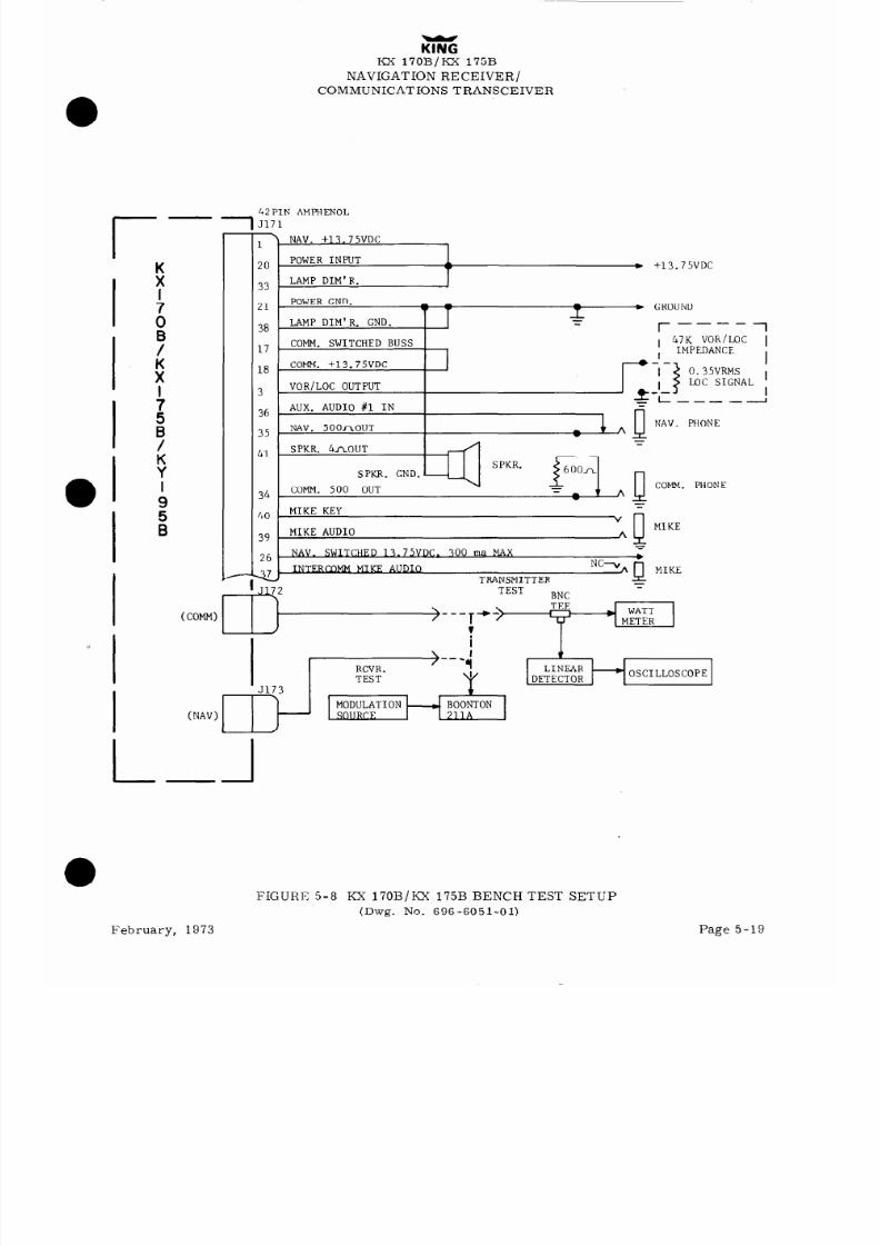
8/9/2019 KX 170A - Maintenance Manual Honeywell
http://slidepdf.com/reader/full/kx-170a-maintenance-manual-honeywell 428/586
r
-e
-
1
KlNG
KX 170B/KX 175B
NAVIGATION RECEIVER/
COMMUNICATIONS TRANSCEIVER
42PIN AMPHENOL
5171
1\ NAV. +13.75VDC
20
POWER INPUT
m +13.75VDC
33
LAMP DIM'R.
21
POWERGND.
T
LAMP DIM'R. GND.
1
e GROUND
38
T
r----i
17 L
COMM. SWITCHED BUSS
, 47K
VORiLOC 1
18
COMM. +13.75VDC
I
I
IMPEDANCE
--
l
I
0.35vEws ,
3
VOR/LOC OUTPUT
n
LOC SIGNAL
&----_1
36
AUX. AUDIO #l IN
35
NAV. 500noUT
bin
NAV. PHONE
SPKR. 4noUT
=
41
SPKR.
SPKR. GND.
600n
34
COMM. 500
OUT =
v 4
COMM. PHONE
-
LINEAR
DETECTOR
OSCILLOSCOPE
February, 1973
FIGURE 5-8 KX 170B/KX 175B BENCH TEST SETUP
(Dwg. No. 696-6051-01)
Page 5-19

8/9/2019 KX 170A - Maintenance Manual Honeywell
http://slidepdf.com/reader/full/kx-170a-maintenance-manual-honeywell 429/586
KlNG
KX 170B/KX 175B
NAVIGATION RECEIVER/
COMMUNICATIONS TRANSCEIVER
5. 2. 8
Kx 170B/KX 175B & Test Data
(Refer to the Installation Manual for Technical Characteristics)
COMMUNICATIONS TRANSCEIVER
Serial No.
Preliminary Visual Inspection:
a.
Hardware:
(ok)
b.
Input Voltage: VDC
L
Receiver Sensitivity:
a.
s-+-n/n:
118. OOMHz db
119. 95MHz
db
126. 70MHz
db
Date
Paperwork
(ok)
134.
135.
OOMHz
97MHz
db
db
R
2.
3.
b. Quieting: db (frequency =126. 7)
AGC Characteristics:
db
(frequency = 126. 7)
Selectivity:
a.
6db Bandwidth: 126. 70MHz: Above
kHz
Below
kHz
60db Bandwidth: 126. 70MHz: AGC reference voltage
VDC
Above
kHz
Below kHz
4.
Adjacent Channel: 126. 725MHz: db
126. 675MHz db
Adjacent 50kHz Channel: 126. 75MHz db 126. 65MHz db (Kx 170B)
Manual Gain Control: mw max.
watts min.
5.
Headphone Audio: mw
6.
Squelch: a.
Carrier/Noise Squelch set for
pv (2. 7. 1)
b.
Carrier /Squelch set for
PV.
(2. 7. 2)
C.
Squelch Test
(ok)
(2. 7. 5)
Transmitter Frequency Stability after a two hou
tolerance is X). 6OOKHz:
118. 000 kHz 125.475
kHz
119. 025
kHz 126. 975 kHz
120.050 kHz 127. 000 kHz
121.075
kHz 128. 500
kHz
122.100 kHz 129. 625 kHz
123. 225 kHz 130. 750 kHz
124. 350 kHz
r off period at +25”C the allowable
131. 875 kHz
132. 900 -kHz
133. 925 -kHz
134. 950 -kHz
135. 975
kHz
Page 5-20
Rev. 4, January, 1976

8/9/2019 KX 170A - Maintenance Manual Honeywell
http://slidepdf.com/reader/full/kx-170a-maintenance-manual-honeywell 430/586
KlNG
ICX 170B/KX 175B
NAVIGATION RECEIVER/
COMMUNICATIONS TRANSCEIVER
7.
8.
Aux. Audio: #l watts min.
#2
watts min.
#3
watts min.
Intercom: watts min. 5 Watts Min With Standard Mic Signal.
Transmitter:
1.
Power Out:
118. OOMHz
watts
126.45MHz watts 135. 975MHz watts
Low Voltage:
118. OOMHz watts
126. 45MHz
watts
135. 975MHz
watts
2.
Modulation: Capabilities
a.
b.
Microphone: Input VRMS
118. OOMHz
%
126. 50MHz
%
127. 5OMHz
-
70
135. 975MHz
%
C.
Sidetone:
mw min.
mw final adjust
mw max.
Hardware ok
Paperwork ok
Glyptol ok
Test Stamp ok
Rev.
4, January, 1976
Tested by
Inspected by
Page 5-21

8/9/2019 KX 170A - Maintenance Manual Honeywell
http://slidepdf.com/reader/full/kx-170a-maintenance-manual-honeywell 431/586
KlNG
Icx 170B/KX 175B
NAVIGATION RECEIVER/
COMMUNICATIONS TRANSCEIVER
NAVIGATION RECEIVER
Serial #
Date
Preliminary Visual Inspection
a.
Hardware
(ok) b.
Paperwork
(ok)
Input voltage
VDC.
OMNI
1.
SMO Test:
All channels checked
(ok)
108. 00
MHz (frequency)
117.95
MHz (frequency)
(92. 8125MHz *2kHz)
(102. 7625MHz f2kHz)
2.
LOC Input Level:
Set for
VRMS
3.
AG C Characteristic:
degrees
4.
Course Accuracy:
A
0, B
0.
5.
Sensitivity:
117. 95MHz
PV.
LOCALLZER
1.
Sensitivity:
108. 1OMHz
PV.
2.
Centering Accuracy:
A
,B
needles width.
3.
Low Voltage Characteristic:
needles width.
AUDIO
1.
2.
3.
4.
4. 1
5.
Sensitivity:
108. 10MHz
db 117. 95MHz
db
Quieting:
117. 95MHz
db
AGC Characteristic:
117. 95MHz
db
Audio Output:
watts min. undistorted
mw max. fully CCW
Headphone Output:
mw.
Ident/ Voice:
db tone ratio
Page 5-22
Rev. 4, January, 1976

8/9/2019 KX 170A - Maintenance Manual Honeywell
http://slidepdf.com/reader/full/kx-170a-maintenance-manual-honeywell 432/586
KlNG
Kx 170B/KX 175B
NAVIGATION RECEIVER/
COMMUNICATIONS TRANSCEIVER
6.
Selectivity:
6db Bandwidth 112. 50MHz reference, +
kHz -
kHz
Bandwidth at 112. 5OMHz reference AGC Ref. Voltage
112. 55MHz
db 112.45MHz
db
MECHANICAL:
1.
Numberal Alignment:
(ok)
2.
DME Switching:
MHz (ok) kHz
(ok)
3. Glideslope Switching:
4.
ILS Energize:
MHz
(ok)
(ok) kHz (ok)
5 50kHz ILS:
(ok)
6.
Pilot Lamps:
(ok)
Hardware
Paperwork
Glyptol
Test Stamp
(ok)
(ok)
(ok)
(ok)
Rev. 4, January, 1976
Page 5-23

8/9/2019 KX 170A - Maintenance Manual Honeywell
http://slidepdf.com/reader/full/kx-170a-maintenance-manual-honeywell 433/586
KlNG
KX 170B/KX 175B
NAVIGATION RECEIVER/
COMMUNICATIONS TRANSCEIVER
0
NO
0
A
4
NAV AUDIO OK COMM AUDIO OK
- YES
T
9
NAV INDICATION OK
NAV. AUDIO OK
COMM AUDIO OK L -
*
TRANSMITTER
TRANSMITTER CW
YES
YES
YES
MODU~AT’ON
SET MIKE
ON I I3 5 MHz WITH -
W’TH ‘I3 5 MHz
‘020 Hz, 30%
) ON ALL KHz t 20ea)
YES
YES
- ‘26.700 MHz
- ALL KHz (40ea.I c
CW POWER OK AT YES FREO.OK ON ALL
CAPABILITY
YES
NO
POT
STANDARD NAV. SIG.?
MHz(Bea) AND ALL
(VOICE / IDENT) ?
AND ALL MHz (IO ea)?
NO
OK WITH IKHz
1020 Hz, 30% ‘?
ALL MHz ( I8 ea)?
m
‘26.700MHz ?
KHz FRED ‘40eo)? -
(.I25 VRMS)?
PER SEC
I
I
I
1
.
NAV. AUDIO OK
CHECK VORILOC
ON
YES
LEVELADJUST
L
YES
r-i
REPAIR
VOLTAGE
REGULATOR
I
f
1
VOLTAGE REGULATOR 3 VOLTA\GE REGULATOR
OK?
OK ?
I
CHECK
1
YES
Y
INTERCONNECT
NO
ON-OFF SWITCH
I
NO
b
1
+
DETECTO;NAUDIO OK
I ‘3 5 MHz ?
NO
AUDIO OK ON
PIN 35 OF Jl7’ ?
CHECK
YES INTERCONNECT,
- RELAYS,ON-OFF SW.,
AUDIO POWER AMPL.
REPAIR AUDIO
- AMPL. CIRCUITRY
NO
(I 403)
I
I
I
c
‘SNAV SMO
CHECK NAV. SMO
INJECTION
NO
- SEE
*
FREQUENCY
SEC. 5.4
CORRECT ?
I
YES
REPAIR NAV.
n
ECEIVER
PER
SECTION 5.6
VOLTAGE
13.75VDC TO
1
I
REGULATOR
VOLTAGE
OK?
REGULATOR
OK?
INJECTION FREO
(135.700MHZ)
CORRECT 7
YES
b
DETECTORETECTOR
DOES CR431OES CR431
AUDIOUDIO
= HAVE FORWARDHAVE FORWARD
OK? TP4lOK? TP4lO
BIAS VOLTAGE? LIAS VOLTAGE? L
I
NO
TRANSMITTER
NO
REPAIR AS IN
COAX $ DIODE
-
SEC. 5.9
SWITCH OK?
I
YES
- -
13-75 VDC TO
NO
H
CHECK RELAY
INTERCONNECT
TRANSMITTER
OK ?
I
TRANSMITTER TROUBLESHOOT
YES
EXCITATION LEVEL -
TRANSMITTER
AND FREQ. OK?
PER SEC. 5.9
7
CHECK
w
_1
YES
COMM SMO
1
PER SEC 5.5
l
I
IAL 135.700 AND
APPLY IOOy. IS COMM NO
SMO INJECTION FREQ
1 coRREcr~i26700MHZ,~
CHECK MODULATOF;
PER SEC. 5.8
I
PER SEC 5.7
I
FIGURE 5-9 TROUBLESHOOTING FLOW CHART
(Dwg. No. 696 -6 110 -00)
Rev. 4, January, 1976 Page 5-25

8/9/2019 KX 170A - Maintenance Manual Honeywell
http://slidepdf.com/reader/full/kx-170a-maintenance-manual-honeywell 434/586
K?NG
KX 170B/KX 175B
NAVIGATION RECEIVER/
COMMUNICATIONS TRANSCEIVER
5.3 TROUBLESHOOTI#6HE KX 17OB/KX 1758
Figure 5- 9 is a troubleshooting flow chart designed to aid the technician in sectionalizing or
localizing sources of trouble. NAV and COMM block diagrams Figure 5-24 and 5-25 appearing
at the end of Section 5 may also aid in localizing the malfunction, The troubleshooting charts
(Table 5-5 thru 5-9) are given as a quick guide in pinpointing probable problem areas along with
their associated remedies. A list of possible SMO malfunctions is given in the Preliminary
Evaluation section o f the respective SMO discussions (NAV SMO, Section 5,4, COMM SMO,
Section 5. 5).
Individual circuit tracing and isolation of a defective component is most easily accomplished by
use of the individual troubleshooting sections, along with appropriate schematic diagrams appear-
ing at the end of Section 5.
February, 1973
Page 5-27

8/9/2019 KX 170A - Maintenance Manual Honeywell
http://slidepdf.com/reader/full/kx-170a-maintenance-manual-honeywell 435/586
KlNG
KX 170B/IOI 175B
NAVIGATION RECEIVER/
COMMUNICATIONS TRANSCEIVER
TABLE 5-5 NAV SMO TROUBLE CHART
[NDICATION
Low or no output from
Receiver Buffer
Correct output on lower
frequencies only.
PROBABLE CAUSE
Voltage Regulated Supply
(8. 5 and 5 . 0 volts) com-
ponent failure.
Receiver Buffer com-
ponent failure
VCO adjusted incorrectly.
REMEDY
Check QlOl, Q103 and
CR214 voltages and
associated components.
Check Q202 voltages and
associated components.
Check VCO adjustment
L201.
See Alignment
Procedure.
Frequency incorrect on
some positions of NAV
MHz and KHz frequency
cant rol.
Switching wafer defective.
Check switch wafer S107
rear for MHz error. See
Table 4-3. (KX 170A/175
Manual)
Check switch wafer S105
for KHz error. See Tab1
4-3. (KX 170A/KX 175
Manual)
Programmable Divider
component failure.
Check 1201, I202, 1203,
1304 and 1206. See
Troubleshooting Procedui
Frequency error and/ or
jitter in Receiver Buffer-
output.
Phase and Frequency com-
parator component failure.
Check 1210, 1211, and
1212 voltages and asso-
ciated components.
Check output at R215 witl-
an oscilloscope and
observe waveform when
switching NAV MHz
frequency control.
Frequency error in
Low Reference Oscillator
Receiver Buffer output,
400KHz component failure.
Check Q210 and Q211
voltages and associated
components.
Check Y202 frequency at
TP205
High Reference Oscillator
53. 93125MHz component
failure.
Check Q207 voltages and
associated components.
Check Y201 frequency at
junction of R230 and R233
Page 5-28

8/9/2019 KX 170A - Maintenance Manual Honeywell
http://slidepdf.com/reader/full/kx-170a-maintenance-manual-honeywell 436/586
KlNG
KX 170B/KX 175B
NAVIGATION RECEIVER /
COMMUNICATIONS TRANSCEIVER
TABLE 5-5 NAV SMO TROUBLE CHART (Cant)
INDICATION
PROBABLE CAUSE
Divide by 2 Mixer and
amplifier component failure.
Squaring Amplifier com-
ponent failure.
Voltage Translator com-
ponent failure.
VCO Low Pass Filter com-
ponent failure.
TABLE 5-6 COMM SMO TROUBLE CHART
INDICATION
Low or no output from
Receiver Buffer
Receiver Buffer output
but no Transmit Buffer
output in Transmit
condition.
Transmit Buffer output
in Receiver Condition
PROBABLE CAUSE
Voltage Regulated Supply
(8:5 and 5. 0 volts) com-
ponent failure.
Receiver Buffer component
failure.
Transmit Buffer component
failure.
Transmit Enable Switch
component failure.
Out of Lock Disable
Transmit Enable Tran-
sistor open.
REMEDY
Check Q206 voltages and
associated components,
Check for frequency input
at TP203 and for divide
by 2 frequency output at
T P204.
Check Q208 and Q209 VOlti
ages and associated comp-
onents. Use an oscillo-
scope and check for an
essentially square wave
output at TP206.
Check Q212 voltages and
associated components.
Connect oscilloscope to
TP202 and observe wave-
forms when switching
NAV MHz frequency
control.
Check at TP201 for a dc
voltage change as the
NAV MHz frequency con-
trol is switched.
Check Q102, Q105, Q104
and CR319 voltages and
associated components.
Check Q303 voltage and
associated components,
Check Q306 voltages and
associated components.
Check Q305 voltages and
associated components.
Check Q307 and input to
R323 with an oscilloscope
Check Q305 voltages.
February, 1973 Page 5-29

8/9/2019 KX 170A - Maintenance Manual Honeywell
http://slidepdf.com/reader/full/kx-170a-maintenance-manual-honeywell 437/586
KING
Kx 170B/hX 175B
NAVIGATION RECEIVER/
COMMUNICATIONS TRANSCEIVER
TABLE 5-6 COMM SMO TROUBLE CHART (Cont)
Receiver Buffer and/or
Transmit Buffer, fre-
quency incorrect from
118. 00 to 126. 95MHz
but OK from 127. 00 to
135MHz or vice versa.
COMM MHz HI-LO switch
Transmit-Receive Relay
High Reference Crystals
Check switch wafer S103
Check relay K701.
Check Y301 and Y302 and
associated components.
Check switching diodes
CR313, CR314, CR321,
and CR322 bias voltages.
HI-LO VCO Switch
Check switching diodes
CR301 and CR302 bias
VCO adjusted incorrectly.
Check VCO adjustments
C314 and C315. See
Alignment Procedure.
Frequency incorrect
on some positions of
COMM MHz and/or
KHz frequency control.
Switching Wafe r defective,
Check switch wafer S103
for MHz error.
Check switch wafer SiOl
and S102 for KHz error.
See Table 4-3.
Programmable Divider
component failure,
Check 1301, 1302, 1303,
1304, 1306 and 1309. See
Troubleshooting Procedul
Frequency incorrect
on XXX. X0 or XXX. X5
Positions
Stable frequency error
in Receiver and T rans-
mit Buffer output.
Programmable Divider
Component Failure
Low Reference Oscillator
400KHz, (in NAV SMO
KX 170B) (in COMM SMO
KX 175B).
Check 1309 and 1303C
See Troubleshooting
Procedure,
Check for 400KHz input tc
TP305 (from NAV SMO
KX 170B) (Q315 and Q31’6
voltages and associated
components KX 175B).
High Reference Oscillator
component failure.
Check Q311 voltages and
associated components.
Check output at junction
of CJ301 and CJ302.
Frequency error and, 3r
jitter in Receiver and
Transmitter Buffer output.
--.:
Phase and Frequency
C lmparator component
failure,
-Check 1310, 1311, and
1312 voltages and asso-
ciated components.
Page 5-30
February, 1973

8/9/2019 KX 170A - Maintenance Manual Honeywell
http://slidepdf.com/reader/full/kx-170a-maintenance-manual-honeywell 438/586
.
KlNG
ICC 170B/KX 175B
NAVIGATION RECEIVER/
COMMUNICATIONS TRANSCEIVER
TABLE 5-6 COMM SMO TROUBLE CHART (Cant).
INDICATION PROBABLE CAUSE
REMEDY
Check output at R323 witk
an oscilloscope and ob-
serve waveform when
switching COMM MHz
frequency control.
Frequency error and/or
jitter in Receiver and
Transmitter Buffer output.
Low Referen’ce Oscillator
400KHz (in NAV SMO KX 170B)
(in COMM SMO KX 175B)
Check for 400KHz input tc
T P305.
High Reference Oscillator
component failure.
Check Q311 voltages and
associated components.
Check output at junction
of CJ301 and CJ302.
Divide by 2 Mixer and
amplifier component
failure.
Check Q310 voltages and
associated components.
Check for frequency inpul
at Q304 collector and for
divide by 2 frequency out
put at TP304.
Squaring Amplifier com-
ponent failure.
Check Q312 and Q313
voltages and associated
components
Use an osc
illoscope and check for al
essentially square wave
output at TP305.
Voltage Translator com-
ponent failure.
Check Q317 voltages and
associated components.
Connect oscilloscope to
TP302 and observe wave-
form when switching
COMM MHz frequency
control.
VCO Low Pass Filter
Component Failure
Check at TP301 for a dc
voltage change as the
COMM MHz frequency
control is switched.
February, 1973 Page 5-31
8/9/2019 KX 170A - Maintenance Manual Honeywell
http://slidepdf.com/reader/full/kx-170a-maintenance-manual-honeywell 439/586
KlNG
KX 170B/KX 175B
NAVIGATION RECEIVER/
COMMUNICATIONS TRANSCEIVER
TABLE 5-7 NAV RECEIVER TROUBLE CHART
See Table 5-7 of KX 170A/KX 175 Maintenance/Overhaul Manual
TABLE 5-8 COMM RECEIVER TROUBLE CHART
See Table 5-8 of Kx 170A/KX 175 Maintenance/Overhaul Manual
TABLE 5-9 COMM TRANSMITTER TROUBLE CHART
See Table 5-9 of KX 170A/KX 175 Maintenance/Overhaul Manual
5.4 TROUBLESHOOTINHE NAV SMO
The KX 170B/KX 175B NAV SMO analog circuitry is identical to that of the KX 170A/KX 175 .
See the KX 175 Maintenance Manual fo r troubleshooting procedures not covered in this section.
5. 4. 1
PRELIMINARY EVALUATION (Figure 5-27)
See paragraph 5. 5. 1 of KX 175 Manual.
5. 4. 2
NAV SMO DIAGNOSTIC PROCEDURE
If the tests of 5. 4. 1 substantiate the NAV SMO failure, proceed as follows:
A.
B.
C.
D.
E.
F.
G.
II.
Open the loop.
High Reference Oscillator
Low Reference Oscillator
VCO and Receiver Buffer
Divide by 2
Mixer
See Paragraph 5. 5. 2,
A through G of KX 175
Manual.
Squaring Amplifier
J
Does the Programmable Divider Provide Proper Frequency Division?
Maintain the channel setting and the VCO tuning voltage of Steps D through G.
Attach the oscillo-
scope probe to Pin 9 of 1202 or 1206 to monitor the counter output.
The waveform of Figure 5- 10
should be obtained. Note the pulse period of approximately 40psec. Dial the ten MHz positions,
leaving the VCO bias unchanged,
and look for the counter output pulse rate to increase uniformly
as lower channel frequencies are dialed.
Return the MHz dial to the 116MHz position and dial
through the twenty KHz positions.
Observe a gradual advance in output pulse rate as numbers
are dialed from the 0. 95 to . 00 using counterclockwise rotation.
If erroneous operation of the Programmable Counter is observed,
service the counter using the
procedure of Section 5. 4. 3.
Page 5-32
February, 1973

8/9/2019 KX 170A - Maintenance Manual Honeywell
http://slidepdf.com/reader/full/kx-170a-maintenance-manual-honeywell 440/586
KlNG
KX l’IOB/KX 175B
NAVIGATION RECEIVER/
COMMUNICATIONS TRANSCEIVER
Horizontal: 5,usec /div
Trace: 1202 or 1206 Pin 9
Vertical: 2V /div
FIGURE 5-10 PROGRAMMABLE DIVIDER OUTPUT
(Dwg. No. 696-6111-00)
I.
Is the Phase and Frequency Compara tor Operational?
Connect the oscilloscope probe to the junction of Pins 4, 9 and 11 of 1211 and R215 to monitor the
Phase and Frequency Comparator output. With the channel selector at 116. 70MHz, vary the
VCO bias voltage above and below 6. 50 volts.
The output voltage on the scope should be dominat-
ely low wheri the VCO bias is low,
and high when the VCO bias is high.
Waveforms are illustrat-
ed in the Phase and Frequency Compara tor Timing Diagrams of Figure 5-23.
If a malfunction is
noted, troubleshoot the circuit as illustrated in Section 5. 4.4.
J.
Does the Voltage Translator Operate Properly?
Repeat the test of Step I but with the oscilloscope probe attached to TP202.
Waveforms are
illustrated in Figure 5-11. Service the circuit as required using the reference information of
Section 5. 4. 8.
Horizontal: 1Oysec /div
Upper Trace: Comparator Output
(Pins 4, 9, & 11 of 1211)
Upper Vertical: 5V /div
Lower Trace :
Translator Output (TP202)
Lower Vertical: 2V /div
FIGURE 5 - 11 VOLTAGE TRANSLATOR
(Dwg. No. 696-6112-00)
K.
What if no Problems are Observed?
Troubleshoot the remaining block, the VCO Low Pass Filter per the discussion of Section 5. 4. 7.
February, 1973
Page 5-33

8/9/2019 KX 170A - Maintenance Manual Honeywell
http://slidepdf.com/reader/full/kx-170a-maintenance-manual-honeywell 441/586
KlNG
KX 170A/KX 175B
NAVIGATION RECEIVER/
COMMUNICATIONS TRANSCEIVER
5. 4. 3
PROGRAMMABLE DIVIDER, NAV (Figure 5-27)
The Programmable Divider consists of integrated circuits 1201, 1202, 1204, 1206 and gates A and
D in 1203.
Reference material includes the divider theory of Section 4 and the Timing Diagram
of Figure 5 -20,
5. 4. 3. 1 Troubleshooting Procedure.
I
.
Test Setup
A.
Open either end of L204, the Mixer LOW Pass Filter choke.
B.
Use a coaxial pigtail to connect an HP 606A, or equivalent, to the tie point of C240 and
C241.
II.
Equipment Adjustments
A. Using a frequency counter, set the 606A, to a CW frequency of 3. 175MHz.
B.
Adjust the HP 606A CW level to obtain a crisp square wave (0 volts base line, 4 volts
peak line) at TP206, when viewed by a 30MHz bandwidth or wider oscilloscope.
C.
Dial the NAV channel selector to 116. 70MHz.
III. Observations
A.
Use a 30MHz bandwidth (or wider) oscilloscope.
Provide external sync from the lead-
@
ing edge of the pulse appearing at 1202 or 1206 Pin 9.
B.
Compare the waveform at Pin 6 of 1204 to the timing diagrams.
(Figure 5-20) The
desired output is a pulse train with a 4 volt reference level, a 40psec period (25KHz
rep rate), negative pulse width of approximately 2lOnsec, and 0 volts negative excur-
sion.
C.
If the desired oscilloscope trace was obtained in B,
the counter is operational at
116. 70MHz.
Dial 117. 950MHz. With the oscilloscope sync as in A,
simultaneously monitor TP206 and Pin 9 of 1202 or 1206.
Note the relationship
of the pulses as the dial is rotated sequentially to the next lowest channel.
The output
pulse (Pin 9 of I202 or 1206) should step 1 input pulse increment with each 50KHz step
in dialing,
t ional.
See Figure 5-12.
If the counter meets the above requirements it is opera-
D.
Failure to meet the requirements of Step B requires a complete check of the I-C input/
output timing as defined in the Timing Diagram (Figure5 -20).
E.
Failure to meet the requirements of Step C implies a problem with the preset function
of the Programmable Divider.
Make a complete check of the divider flip-flops im-
mediately preceding and following the preset enable pulse (negative pulse on pin 6 of
1204.
The desired preset states are defined in Table 4-3 (KX 175 Manual) where 0 is
ground and 1 is 5 volts, and should occur immediately following the preset enable
pulse.
Also review Figure 5-20.
F.
Replace components and make repairs as necessary to obtain the desired counter
operation.
a
Page 5-34
February, 1973

8/9/2019 KX 170A - Maintenance Manual Honeywell
http://slidepdf.com/reader/full/kx-170a-maintenance-manual-honeywell 442/586
KX l’IOB/KX 175B
NAVIGATION RECEIVER/
COMMUNICATIONS TRANSCEIVER
Selected Freq. =116. 70MHz
Selected Freq. =116. 65MHz
Vertical:
Top-2V /div (TP206)
Bottom-
2V/div (Pin 9 of 1202 or 1206)
HorizontaI: 0. 5p set /div Expanded X 10
FIGURE 5-12 PROGRAMMABLE DIVIDER
(Dwg. No. 696 -6 113 -00)
5. 4. 4 PHASE
AND FREQUENCY COMPARATOR (Figure
5-27)
The Phase and Frequency Comparator consists of 1211 and 1212.
Reference information sources
include the Phase and Frequency Comparator Timing Diagram (Figure 5-23) and the theory of
section 4. 2.
-NOTE-
If the COMM SMO is operating properly it
may be used to provide supplementary in-
formation using comparison techniques.
5. 4.4. 1 Troubleshooting Procedure
A.
Connect an external power supply to the VCO bias test point TP201.
B.
Set the NAV Frequency Selector to 116. 70MHz.
C.
Monitor the Compara tor output (Pins 4, 9, or 11 of I21 1) on an oscilloscope.
D. Adjust the VCO bias voltage low (less than 6. 50 volts) and look for a low output voltage
(around . 2 volts).
Refer to Figure 5-23 for the appropriate timing diagram.
E.
Adjust the VCO bias voltage high (greater than 6. 50 volts) and look for a high voltage out-
put voltage (near 4. OV).
Refer to Figure 5-23 for the- appropriate timing.
F.
Failure to meet the conditions of Steps C and D requires a systematic comparison of the
input (output) relationships obtained to those appearing in either the Timing Diagram or the
functioning COMM SMO.
February, 1973
Page 5-35

8/9/2019 KX 170A - Maintenance Manual Honeywell
http://slidepdf.com/reader/full/kx-170a-maintenance-manual-honeywell 443/586
KX 170B/KX 175B
NAVIGATION RECEIVER/
COMMUNICATIONS TRANSCEIVER
5. 4. 5
LOW REFERENCE OSCILLATOR (Figure 5-27 NAV) (5-29, COMM)
The
Low Reference Oscillator consists of transistors Q210 (Q315) and Q211 (Q316). with crystal
Y202 (Y303) as the frequency determining element.
The Low Reference Oscillator serves both
the NAV and COMM SMO’s. (KX 170B only).
5. 4. 5. 1
Troubleshooting Procedures.
Using an oscilloscope check TP205 (TP305) for a square wave output (See Figure 5-15).
Capa-
citively couple a frequency counter to TP205 (TP305) and check for 400KHz.
Check Q210 (Q315)
and Q211 (Q316) and the associated circuitry.
See Figure 5-27 and 5-29 for typical D-C operat-
ing voltage levels.
5. 4. 6
VOLTAGE CONTROLLED OSCILLATOR (VCO) (Figure 5-27)
The Voltage Controlled Oscillator (Q201) is a Colpitts oscillator.
Frequency determining
elements include CR201, L201, C204 and C205.
Basic theory appears in Section 4. 2. 2. 2.
5. 4. 6. 1
Troubleshooting Procedure.
Compare the supply and bias voltages for Q201 with those appearing in Figure 5-27 and replace
components as necessary to obtain proper bias.
Apply a 7. 2 volt tuning bias voltage, from a
low impedance source, to TP201 and use a frequency counter to monitor the frequency at the
collector of Q201.
Adjust L201 to obtain a frequency of approximately 102. 7625.
The VCO
frequency should vary proportionately.as the tuning voltage is varied.
If erratic or erroneous
operation is obtained, check the frequency determining elements.
Failure of the VCO to oscil-
late implies an open varactor diode (CR201), an open trimmer coil (L201), or a bad transistor
(Q201).
5.11’:’ VCO LOW PASS FILTER (Figure 5-27)
The VCO Low Pass Filter consisting of T201, T208, C211, C212, C213 and C271 is a low pass fil-
ter designed to recover the D-C voltage from the output of the 25KHz Voltage Translator.
It
has been factory adjusted and no attempt should be .rrade to readjust in the field.
5.4. 7.1
Troubleshooting Procedure.
TP202. Using a D-C voltmeter,
Using an oscilloscope, check wave form of the input at
check for a D-C voltage at TP201 (7. 20VDC at 117.95MHz to
2.84VDC at 108. OOMHz).
5.4.8 25KHz VOLTAGE TRANSLATOR (Figure 5-27)
The Voltage Translator consists of transistor Q202 which shifts the error voltage level from
the Phase and Frequency Comparators to a level sufficient to operate the VCO.
5.4.8.1
Troubleshooting Procedure.
to the output of TP202.
Using an oscilloscope trace the input signal from R215
See Figure 5-27 for typical D-C operating voltage levels.
5.4.9 RECEIVER BUFFER (Figure 5-27)
The Receiver Buffer consists of transistor, Q202, with output transformer,
T202.
5.4. 9.1 Troubleshooting Procedure.
to the output at Pin 2 of T202.
Using an oscilloscope, trace the input signal from C216
See Figure 5-27 for typical D-C operating voltage levels.
Page. 5-36 February, 1973

8/9/2019 KX 170A - Maintenance Manual Honeywell
http://slidepdf.com/reader/full/kx-170a-maintenance-manual-honeywell 444/586
KX 170%Ng 175B
NAVIGATION RECEIVER/
CC&IMUNICATIONS TRANSCEIVER
5. 4. 10 VCO BUFFER (Figure 5-27)
The VCO Buffer consists of transistor Q203 with output transformer T203.
5. 4. 10. 1 Troubleshooting Procedure. Using an oscilloscope, trace the input signal from
C220 to the output at T203. See Figure 5-27 for typical D-C operating voltage levels.
5. 4. 11 HIGH REFERENCE OSCILLATOR (Figuref5- 27)
The High Frequency Oscillator consists of transistor Q207 connected in a typical Colpitts con-
figuration with crystal Y201 determining the operating frequency.
5. 4. 11. 1 Troubleshooting Procedure. Check Pin 6 of T207 for oscillator output. Check
supply and biasing voltage (See Figure 5-27 for typical D-C operating voltage levels. )
5. 4. 12 IMPLICIT DIVIDE BY 2 CIRCUIT (Figure 5-27)
The Implicit Divide by 2 circuit consists of balanced mixer CR203, CR204, CR205 and CR206
and amplifier $206.
For circuit theory refer to Section 4. 2.
5. 4. 12. 1 Troubleshooting Procedure.
Using an oscilloscope verify the output of VCO
Buffer at Pin 6 of T204.
See Figure 5-27 for typical D-C operating voltage levels.
:. 4. 13 2ND MIXER (Figure 5-27)
This is a balanced mixer consisting of transformer T206 and T207 with diodes CR207, CR208,
CR209 and CR210.
5. 4. 13. 1 Troubleshooting procedure.
With the power removed from the KX 170B /KX 17 5B
and using an ohmmeter, check all diodes for a possible open.
Check all transformer windings
for D-C continuity.
5. 4. 14 MIXER LOW PASS FILTER (Figure 5-27)
The Mixer Low Pass Filter is a basic pi-section low pass filter consisting of inductor L204 and
capacitors C239 and C240.
5. 4. 14. 1 Troubleshooting Procedure.
Using an oscilloscope trace the signal from the out-
put of the 2nd Mixer (Pin 2 of T206) to the input of the Squaring Amplifier (base Q208).
5. 4. 15 SQUARING AMPLIFIER (Figure 5-27)
The Squaring Amplifier consists of transistors Q208 and Q206.
5. 4. 15. 1 Troubleshooting Procedure.
Using an oscilloscope check for Mixer output at the
base of Q208. Check TP206 for a 4 volt square wave output.
Check transistor Q208 and Q209
and associated circuitry.
See Figure 5-27 for typical D-C operating voltage levels (with the
base of Q208 bypassed).
5.5 TROUBLESHOOTINHE COMMSMO
The COMM SMO synthesizes 720 frequencies, providing a power level of 10mw into a 5Ofi load.
The relationship of channel frequency to synthesized frequency is illustrated in Table 5-10.
Theory of Operation is presented in Section 4.
February, 1973
Page 5-37

8/9/2019 KX 170A - Maintenance Manual Honeywell
http://slidepdf.com/reader/full/kx-170a-maintenance-manual-honeywell 445/586
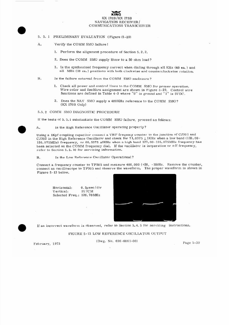
8/9/2019 KX 170A - Maintenance Manual Honeywell
http://slidepdf.com/reader/full/kx-170a-maintenance-manual-honeywell 446/586
KlNG
KX 170B/KX 175B
NAVIGATION RECEIVER /
C OMIVIUNICATIONS TRANSCEIVER
5. 5. 1 PRELIMINARY EVALUATION (Figure (5-29)
A. Verify the COMM SMO failure
1.
Perform the alignment procedure of Section 5.2.2.
2. Does the COMM SMO supply 10mw to a 50 ohm load?
3. Is the synthesized frequency correct when dialing through all KHz (40 ea. ) and
all MHz (18 ea. ) positions with both clockwise and counterclockwise rotation.
B.
Is the failure external from the COMM SMO enclosure?
1.
Check all power and control lines to the COMM SMO for proper operation.
Wire color and feedthru assignment are shown in Figure 5-29.
Control wire
functions are defined in Table 4-3 where “0” is ground and “1” is 5VDC.
2. Does the NAV SMO supply a 4OOKHz reference to the COMM SMO?
(Kx 170B Only)
5.5.2 COMM SMO DIAGNOSTIC PROCEDURE
If the tests of 5. 5.1 substantiate the COMM SMO failure, proceed as follows:
A.
Is the High Reference Oscillator operating properly?
Using a 1Kpf coupling capacitor connect a VHF freqency counter to the junction of CJ301 and
CJ302 in the High Reference Oscillator and check for 71.0375 +lKHz when a low band (118. OO-
126.975MHz) frequency, or 66. 5375 flKHz when a high band 127.00-135.975MHz frequency has
been selected on the COMM frequency dial.
If the oscillator is inoperative or off frequency,
refer to Section 5. 5. 10 for servicing information.
B.
Is the Low Reference Oscillator Operational?
Connect a frequency coi
connect an oscilloscope
Figure 5-13 below.
Horizontal:
0. 5,usec /div
Vertical: IV/CM
Selected Freq
.:
126.7OMHz
inter to TP305
1 and 1 easure 400,000 (+20, -1O)Hz. Remoi
re the
counter,
to TP305 and
obser ‘ve the waveform.
The proper wavefor
m is
shown in
If an incorrect waveform is observed, refer to Section 5.4. 5 for servicing instructions.
FIGURE 5-13 LOW REFERENCE OSCILLATOR OUTPUT
February, 1973
(Dwg. No. 696 -606 l-00)
Page 5-39

8/9/2019 KX 170A - Maintenance Manual Honeywell
http://slidepdf.com/reader/full/kx-170a-maintenance-manual-honeywell 447/586
C.
Open the loop.
KING
KX 170B/KX 175B
NAVIGATION RECEIVER /
COMMUNICATIONS TRANSCEIVER
-NOTE-
To properly troubleshoot the
COMM SMO it is imperative
that the feedback loop be dis-
abled. This is accomplished
very simply by applying a
positive, adjustab le D-C voltage
from a low impedance source
to TP 301, the VCO bias point.
D. Does the VCO and Receiver Buffer perform properly?
Dial 126. 7OMHz on the COMM frequency selector,
and adjust the VCO bias voltage to 6.85V.
Connect a VHF counter to the Receiver Buffer, TP303, and adjust C315 to obtain a frequency
of approximately 135. 70MHz.
Change the COMM frequency selector dial to 135. 70MHz and adjust C314,to obtain a frequency
of approximately 126. 7OMHz. Erratic or improper tuning, or low output should be corrected
by troubleshooting the VCO and/or VCO Buffer as outlined in Sections 5. 5. 5 and 5. 5. 9.
E. Is the Implicit Divide by 2 halving the VCO frequency?
.-
Without altering the tuning voltage or the channel frequency setting, connect the VHF counter
to TP304 and read a frequency of approximately 63.35MHz. Change the COMM frequency
selector dial back to 126.70MHz and read a frequency of approximately 67.85MHz on the
counter. If a malfunction is observed, the circuit may be serviced using the troubleshooting
instructions of Section 5.5.11.
F.
Is the Mixer Working Properly?
With 126. 70 selected and 6.85VDC bias applied to the VCO, as in previous steps, connect an
oscilloscope to the junction of L305, C376 and C377.
The waveform should be one of the
Page 5-40
February, 1973

8/9/2019 KX 170A - Maintenance Manual Honeywell
http://slidepdf.com/reader/full/kx-170a-maintenance-manual-honeywell 448/586
KIN
5;
x 170B KX 175B
NAVIGATION RECEIVER /
COMMUNICATIONS TRANSCEIVER
s
Horizontal:
0. lp set ldiv
Vertical: .05V /div
Selected Freq: 126. 70MHz
FIGURE 5-14 MIXER OUTPUT
(Dwg 696-6062-00)
Failure to obtain the desired trace would indicate a malfunction in the Mixer circuit which can
be serviced using the troubleshooting information of Section 5. 5. 12.
G. Is the Squaring Amplifier Working Properly?
With the VCO oscillating at 135.7OMHz (COMM frequency selector 126. 7OMHz), monitor the
Squaring Amplifier output, TP306, with an oscilloscope having a bandwidth of at least 3OMHz.
If the reference oscillator is functioning properly, the waveform will appear as in Figure 5-15.
If not, troubleshoot the squaring amplifier as in Section 5. 5. 14.
February, 1973
Page 5-41

8/9/2019 KX 170A - Maintenance Manual Honeywell
http://slidepdf.com/reader/full/kx-170a-maintenance-manual-honeywell 449/586
KlNG
KX 170B/KX 175B
NAVIGATION RECEIVER /
COMMUNICATIONS TRANSCEIVER
Horizontal: 0. bsec/div
Vertical:
1V /div
Selected Freq. : 126. 70MHz
FIGURE 5-15 QUARING AMPLIFIER OUTPUT
(Dwg 696-6063-00)
H.
Does the Programmable Divider provide proper frequency division?
Maintain the channel setting and the VCO tuning voltage of steps D through G. Attach the os-
cilloscope probe to the junction of 1304, pin 6; 1302, pin 9; 1306, pin 9, and 1312, pin 3 to
monitor the counter output.
The waveform of Figure 5-16 should be obtained. Note the pulse
period of 401.1 ec.
Dial the eighteen MHz positions,
leaving the VCO bias unchanged, and look
for the counter output pulse rate to increase uniformly as lower channel frequencies are
dialed. Return the MHz dial to the 126MHz position and dial through the forty KHz positions.
Observe a gradual decrease in output pulse rate as numbers are dialed from the 0. 97 to 0.00
using counterclockwise rotation.
If erroneous operation of the Programmable Counter is observed, service the counter using
the procedure outlined in Section 5. 5. 3.
February, 19 73

8/9/2019 KX 170A - Maintenance Manual Honeywell
http://slidepdf.com/reader/full/kx-170a-maintenance-manual-honeywell 450/586
KI G
7
CX 170B KX 175B
NAVIGATION RECEIVER /
COMMUNICATIONS TRANSCEIVER
Horizontal;
5y set /div
Vertical: 2. OV /div
Selected Freq. : 126. 7 MHz
FIGURE 5-16 PROGRAMMABLE DIVIDER OUTPUT
(Dwg 696-6064-00)
I.
Is the Phase and Frequency Compara tor Operational?
Connect the oscilloscope probe to the tie point of Pins 4,
9, and 11 of 1311 and R333 to monitor
the Phase and Frequency Comparator output. With the COMM channel selector at 126.7OMHz,
vary the VCO bias above and below 6.85 volts. The output voltage on the scope should be
dominately low when the VCO bias is low, and high when the VCO bias is high.
Waveforms
are illustrated in the Phase and Frequency Comparator timing diagrams of Figure 5-23. If a
malfunction is noted, troubleshoot the circuit as instructed in Section 5. 5.4.
J. Does the Voltage Translator Operate Properly?
Repeat the test of Step I but with the oscilloscope probe attached to TP302.
Waveforms are
illustrated in Figure 5-17and 5-23. Troubleshoot the circuit as required using the infor-
mation given in Section 5. 5.7.
February, 1973
Page 5-43
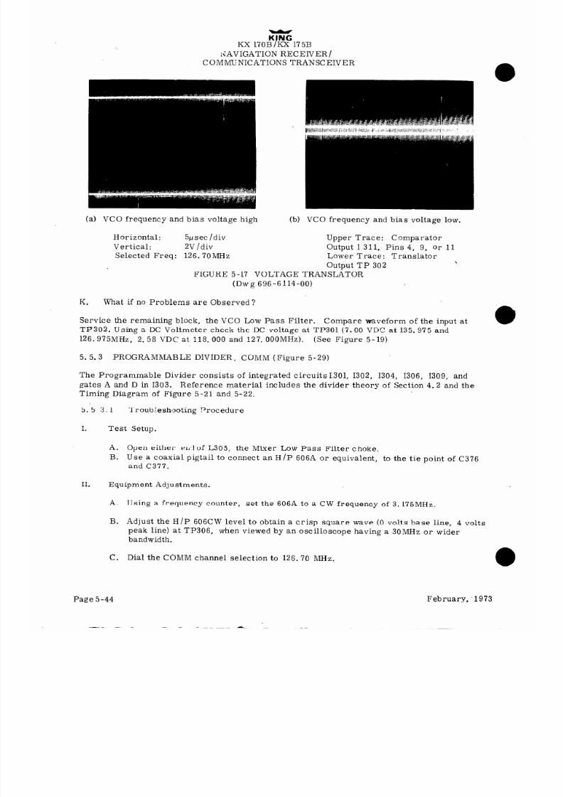
8/9/2019 KX 170A - Maintenance Manual Honeywell
http://slidepdf.com/reader/full/kx-170a-maintenance-manual-honeywell 451/586
K NG
KX 170B KX 175B
;qAVIGATION RECEIVER/
COMMUNICATIONS TRANSCEIVER
(a) VCO frequency and bias voltage high
(b) VCO frequency and bias voltage low.
Horizontal: Sysec /div Upper Trace: Compara tor
Vertical:
2V /div Output I 311, Pins 4, 9, Or 11
Selected Freq: 126.7OMHz
Lower Trace: Translator
Output TP 302
\
FIGURE 5-17 VOLTAGE TRANSLATOR
(Dwg 696-6114-00)
K.
What if no Problems are Observed?
Service the remaining block, the VCO Low Pass Filter.
Compare waveform of the input at
TP302. Using a DC Voltmeter check the DC voltage at TP301 (7.00 VDC at 135.975 and
126.975MHz, 2. 58 VDC at 118. 000 and 127. OOOMHz).
(See Figure 5-19)
5. 5.3
PROGRAMMABLE DIVIDER, CGMM (Figure 5-29)
The Programmable Divider consists of integrated circuitsI.301, 1302, 1304, 1306, 1309, and
gates A and D in 1303.
Reference material includes the divider theory of Section 4.2 and the
Timing Diagram of Figure 5-21 and 5-22.
5:5 3.1
Troubieshooting Procedure
I. Test Setup.
A. Open either en,Jof L305, the Mixer Low Pass Filter choke.
B.
Use a coaxial pigtail to connect an H/P 606A or equivalent, to the tie point of C376
and C377.
II. Equipment Adjustments.
A. Using a frequency counter,
set the 606A to a CW frequency of 3.175MHz.
B. Adjust the H/P 606CW level to obtain a crisp square wave (0 volts base line, 4 volts
peak line) at TP306, when viewed by an oscilloscope having a 3OMHz or wider
bandwidth.
C. Dial the COMM channel selection to 126. 70 MHz.
Page 5-44
February, .1973

8/9/2019 KX 170A - Maintenance Manual Honeywell
http://slidepdf.com/reader/full/kx-170a-maintenance-manual-honeywell 452/586
III. Observations
KlNG
KX 17OB/KX 175B
NAVIGATION RECEIVER/
COMMUNICATIONS TRANSCEIVER
A. Use a 3OMHz bandwidth (or wider) oscilloscope. Provide external sync
from the leading edge of the pulse appearing at the junction of 1304Pin6,
1302 and 1306Pin 9 and I3 12Pin 3.
B. Compare the waveform at Pin 6 of 1304 to the equivalent point in the NAV
SMO or to ‘the timing diagram (See Figure 5-21 and 5-22).
The desired
output is a pulse train with a 40 ~.lsec. period (25KHz rep. rate), at 0 volts
base line, +4.0 volt level.
C.
If the desired oscilloscope trace was obtained in B, the counter is opera-
tional at 126.70MHz. Dial 135. 97MHz. With the oscilloscope sync as in Step
A above, simultaneously monitor TP306 and Pin 9 of 1306.
Observe the
second pulse after the sync pulse. Note the relationship of the pulses as the
dial is rotated sequentially to the next lowest channel (counter-clockwise).
The second output pulse after the sync pulse should move 1 input pulse in-
crement (Top Trace Figure 5-18) with each 25KHz step that is dialed (See
Figure 5-18).
If the counter meets the above requirements it is operational.
It is recommended that Pages 4-6 through 4-8 paragraph 4.2. 2. 6 be studied
at this time.
f = 126. 70
f = 126. 675MHz
D.
February, 1973
Top - (TP 306)
Bottom - Counter Output - Second output after sync.
Vertical - 2V/div
Horizontal 101.1et /Div Expanded X10
FIGURE 5 - 18 PROGRAMMABLE DIVIDER
(Dwg. No. 696 -6 115-00)
Failure to meet the requirements of Step B requires a complete check of
the I-C input/output timing as defined in the timing diagram ( Figure 5-21
and 5-22).
Page 5-45
8/9/2019 KX 170A - Maintenance Manual Honeywell
http://slidepdf.com/reader/full/kx-170a-maintenance-manual-honeywell 453/586
KING
KX l’IOB/KX 175B
NAVIGATION RECEIVER /
COMMUNICATIONS TRANSCEIVER
E.
Failure to meet the requirements of Step C implies a problem with the
preset function of the Programmable Divider. ,A complete check of the
divider flip-flops immediate ly preceding and following the preset enable
pulse (negative pulse on Pin 6 of the 1304). The desired preset states are
defined in Table 4-3, where 0 is ground and 1 is 5 volts and should occur
immediately following the preset enable pulse.
F.
Replace components and make repairs as necessary to obtain the desired
counter operation.
5. 5.4
PHASE AND FREQUENCY COMPARATOR (Figure 5-29)
The Phase and Frequency Comparator consists of 1311 and 1312. Reference information sources
include the Phase and Frequency Comparator Timing Diagram (Figure 5-23) and the theory of
section p. 2.
5. 5.4.1
A.
B.
C.
D.
E.
5. 5. 5
-NOTE-
If the NAV SMO is operating properly
it may be used to provide supplementary
information using compar ison techniques.
Troubleshooting Procedure
Connect an external power supply to the VCO bias test point TP301.
Monitor the Comparator output (Pins 4, 9, or 11 of 1311 on an oscilloscope.
Adjust the VCO bias voltage low (less than 6. 50 volts 122. 50) and look for a low output
voltage (around .2 volts. ) Refer to Figure 5-23 for the appropria te timing diagram.
Adjust the VCO bias voltage high (greater than 6. 50 volts) and look for a high voltage
output voltage (near 4. 5V).
Refer to Figure 5-23 for the appropriate timing diagram.’
Failure to meet the conditions of Steps C and D requires a systematic comparison
of the input (output) relationships obtained to those ap,pearing in either the Timing
Diagram or the functioning NAV SMO.
VOLTAGE CONTROLLED OSCILLATOR (VCO) (Figure 5-29)
The Voltage Controlled Oscillator (VCO) consists of transistor Q302, Varactor diode CR303,
with frequency adjust capacitors C314 and C315 and HI-LO VCO switching transistor Q301.
Diodes CR301 and CR302 disable the VCO transistor Q302 when the COMM frequency selector
wafter is dialed to a nonvalid COMM channel.
In the low portion of the COMM band (118.00 -
126.975MHz), the Hi line is grounded on receive and the
“Lo” line is grounded on transmit.
Therefore, in receive the “Hi” line forward biases CR301 applying bias to Q302 for normal
operation.
CR302 is reverse biased by R346 (High Reference Oscillator Section). In the high
portion of the COMM band (127. 00-135. 975MHz) the
“Lo” line is grounded on receive and the “Hi”
line is grounded on transmit. Therefore, in receive the “Lo” line, forward biases CR302
which again applies bias to Q302. At the same time, the “Lo” line enables VCO switch Q301,
placing trimmer C314 in parallel with C315.
CR301 is reverse biased by R347 (High Reference
Oscillator Section).
a
Page 5-46 February, 1973

8/9/2019 KX 170A - Maintenance Manual Honeywell
http://slidepdf.com/reader/full/kx-170a-maintenance-manual-honeywell 454/586
KlNG
KX 170B/KX 175B
NAVIGATION RECEIVER/
COMMUNICATIONS TRANSCEIVER
5. 5. 5.1
Troubleshooting Procedure. Check the supply and bias voltages of Q302. Check for
proper operation of the Hi-Lo switching wafer and associated diodes CR301 and CR302.
Make repairs as necessary to obtain proper operating conditions.
Supply a 7.0
volt bias voltage from a low impedance source to TP301 and monitor the VCO output frequency
by capacitively coupling a frequency counter to the collector of Q302 with a 1OOpf diskcap.
With
the frequency selector at 126. 97MHz adjust C315 to get a frequency of approximately 135. 975MHz.
If this is unattainable, verify that Q301, is turned off and check the frequency determining ‘ele-
ments, C317, C387, C315, C343, L301, and CR303. Dial 135. 97MHz and adjust C314 to obtain
a VCO frequency of 126:975MHz.
If erratic or erroneous operation is noted, check the frequency
determining components and verify that Q301 is saturated.
If the VCO failes to operate, check
L301 and CR303 and Q302. Check the VCO for a proportional change in frequency with tuning
voltage changes on the low and high bands.
5. 5. 6
Vco LOW PASS FILTER (Figure 5-29)
The VCO Low Pass Filter consisting of T307, T308, C348, C349, C350, C390, and C392 is an
elliptic low pass filter designed to recover D-C voltage from the output of the 25KHz Voltage
Translator.
It has been factory adjusted and no attempt should be made to readjust in the field.
5. 5. 6.1
Troubleshooting Procedure.
Using an oscilloscope, check for a square wave input
at TP302.
Using a D-C voltmeter, check for a D-C voltage at TP301 (7.OOV DC at 126. 97MHz
to 2. 58V DC at 118.OOMHz). (See Figure 5-19)
f = 118.00,127. OOMHz
f = 126. 975,135. 975MHz
TP301 and TP302
Vertical 1 V/Division
Horizontal lOns/Division
FIGURE 5-19 LOW PASS FILTER
(Dwg. No. 696 -6 116 -00)
February, 1973
Page 5-47

8/9/2019 KX 170A - Maintenance Manual Honeywell
http://slidepdf.com/reader/full/kx-170a-maintenance-manual-honeywell 455/586
KlNG
Kx 170B/KX 175B
NAVIGATION RECEIVER
COMMUNICATIONS TRANSCEIVER
5. 5.7
25KHz VOLTAGE TRANSLATOR (Figure 5- 29)
The Voltage Translator consists of transistor Q317 which shifts the error voltage level from the
Phase and Frequency Comparator to a level sufficient to operate the VCO.
5. 5. 7. 1
Troubleshooting Procedure. Using an oscilloscope,
trace the input signal from pins
4, 9, or 11 of 1311 to the output at TP302. See Figure 5-29 for
typical D-C operating voltage
levels.
5. 5. 8
RECEIVER BUFFER (Figure 5-29)
The Receiver Buffer consists of transistor Q303 with output transformer T301.
5. 5.8. 1
Troubleshooting Procedure. Using an oscilloscope, trace the input signal from
R309 to the output at TP303. See Figure 5-29 for typical D-C operating voltage levels.
5. 5. 9 TRANSMIT BUFFER/TX ENABL,E SWITCH/OUT OF LOCK TX DISABLE
The Transmit Buffer consists of Q306 with output transformer T305. It provides drive to the
transmitter only when both the TX Enable Switch, Q305, is turned off and the Out of Lock Disable
switch Q307 is saturated providing an emitter current path to ground.
5. 5. 9. 1
Troubleshooting Procedure. Key the transmitter and use an oscilloscope to track
the signal from T301 to Pin 2 of the output transformer T305.
Using a D-C voltmeter, check
the TX enable switch Q305 for proper operation (Saturated in receive, open in transmit) and
check the Out of Lock Disable Q307 for proper operation (saturated-bringing the emitter resistors
of Q303 and Q306 to ground. See Figure 5-29 for typical D-C operating voltage levels.
5. 5. 10
HIGH REFERENCE OSCILLATOR (Figure 5-29)
The High Reference Oscillator consists of transistor Q3 11 operating in a typical Colpitts con-
figuration.
Crystals Y30 1 and Y302 determine the operating frequency.
In the low portion of
the COMM band (llS.OO-126.975MHz), Y301 is used on receive and Y302 is used on transmit.
In the high portion of the COMM band (127.00-135.975MHz), Y302 is on receive and Y301 on
transmit.
5. 5. 10. 1
Troubleshooting Procedure. -Check the oscillator output at Pin 6 of T306.
The
following table gives the desired functions under the various conditions encountered.
Low Band (llS.OO- 126.975MHz)
Receive
f = 71.0375MHz
“Lo” +8. 5v
“Hi” GND
CR314, CR321 Reverse Biased
CR313, CR322 Forward Biased
High Band (127.00- 135. 975MHz)
Receive f = 66.5375MHz
“Lo” GND
“Hi” +8. 5V
CR3 14, CR32 1 Forward Biased
CR313, CR322 Reverse Biased
Transmit
f = 66. 5375tiIHz
Transmit
f = 71.025MHz
“Lo” GND
“Lo” +8. 5V
“Hi” +8. 5V
“Hi” GND
CR314, CR321 Forward Biased
CR3 14, CR321 Reverse Biased
CR313, CR322 Reverse Biased
CR313, CR322 Forward Biased
l
TABLE 5-11 HIGH REFERENCE OSCILLATOR TROUBLESHOOTING TABLE
Page 5-48
February, 1973

8/9/2019 KX 170A - Maintenance Manual Honeywell
http://slidepdf.com/reader/full/kx-170a-maintenance-manual-honeywell 456/586
KlNG
KX 17OB/KX 175B
NAVIGATION RECEIVER
COMMUNICATIONS TRANSCEIVER
Check supply and biasing voltages (See Figure 5-29 for typical D-C operating voltage levels).
5. 5. 11
IMPLICIT DIVIDE BY 2 CIRCUIT (5-29)
The Implicit Divide by 2 circuit consists of balanced mixer CR305, CR306, CR307 and CR308
and amplifier Q3 10.
For circuit theory refer to Section 4.2.
5. 5. 11. 1 Troubleshooting Procedure. Using an oscilloscope verify output from VCO Buffer
at Pin 6 of T302. Check for signal at the base of Q3 10 and track through the amplifier section
working toward TP304. See Figure 5-29 for typical D-C operating voltage levels. Refer to
5.4.12.1 and 5.4.13.1 for procedure for isolating amplifier and mixer failures.
5. 5.12
2ND MIXER (Figure 5-29)
This is a balanced mixer consisting of transformers T304 and T306 and diodes CR309, CR310,
CR311 and CR312.
5. 5.12.1 Troubleshooting Procedure. With the power removed from the KX 170B/KX 175B
using an ohmmeter check all diodes for a possible open. Check all transformer windings for
D-C continuity.
MIXER LOW PASS FILTER (Figure 5-29)
The Mixer Low Pass Filter is a basic pi-section low pass filter consisting of inductor L305 and
capacitors C375 and C376.
5. 5.13.1 Troubleshooting Procedure. Using an oscilloscope trace the signal from the output
of the Second Mixer (Pin 2 of T304) to the input of the Squaring Amplifier (base of Q312).
5. 5.14
SQUARING AMPLIFIER (Figure 5-29)
The Squaring Amplifier consists of transistors Q312 and Q313.
5. 5.14.1
Troubleshooting Procedure. Using an oscilloscope check for mixer output signal
at the base of Q312. Check TP306 for a 4 volt: square wave output.
Check transistors Q312 and
Q313 and associated circuitry (See Figure 5-29 for typical D-C operating voltage levels).
February, 1973
Page 5-49

8/9/2019 KX 170A - Maintenance Manual Honeywell
http://slidepdf.com/reader/full/kx-170a-maintenance-manual-honeywell 457/586
INPUT
CLOCK PI JLSE
(PIN 2 1201)
50KHz FLIP
FLOP OUTPUT
?j(PIN7 1201)
PRESET FLIP FLOP
Q,(PlN IO 1201)
QO
PIN 15
‘t?%i
(1206)
Ql
PIN 14
Q2.
PIN I3
Q3
,PIN I2
KHz 1204
(PIN 8)
QO
PIN I5
QI
PIN I4
Q2
PIN I3
Q3
LPIN I2
--------
-----------
‘; ‘.*
s
I
:
I
II
u
--
- -
--
--
PRESE;f”$ABLE
(PIN6 1304)
LOAD
STATE
L
/
*
-
SELECTED FREQUENCY: NAV-ll6..700MHz
EXPANDED
SCALE
CORRESPONDING Dlvl DE RATIO- 127
FIGURE 5-20 NAV PROGRAMMABLE DIVIDER TIMING DIAGRAM
(Dwg. No. 696-6117-00)
February, 1973
Page 5-53
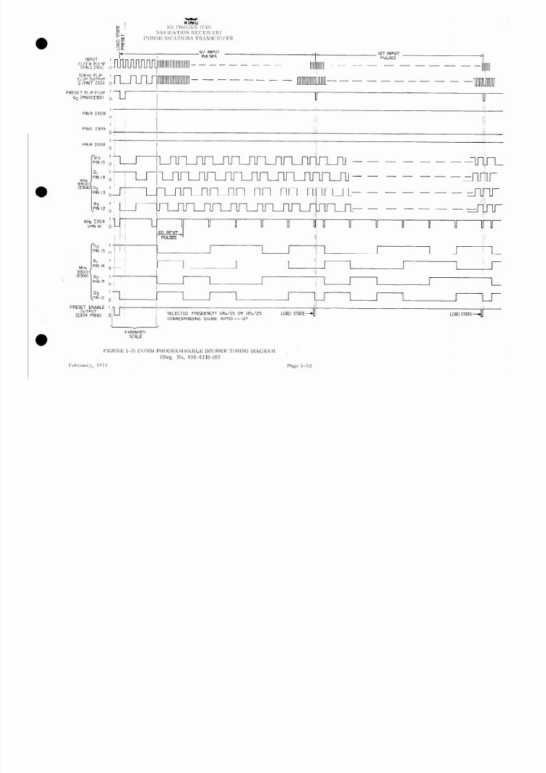
8/9/2019 KX 170A - Maintenance Manual Honeywell
http://slidepdf.com/reader/full/kx-170a-maintenance-manual-honeywell 458/586
127 INPUT
--L
127 INPUT
INPUT
PULSES
CLOCK PULSE
(PIN 2 1301)
I ~,,,,,,,,, ,,,,,,,,,,, ,,,,- “““‘” - - - _ - - - - ,,&,,I, - - - - -
0
50KHz FLIP I
FLOP OUTPUT
0 (PIN7 1301) 0
PRESET FLIP FLOP ’
Q2 (PIN IOI301) o
I
PIN9 1309
u
u
:
‘I
I
0
,
I
8:;
PING 1309 :
0,
I
PIN8 1303 ’
0 :
I
; :
i ,i
I
I
QI
1:
PINl40i j
ul-ltl utl U-u-L-Inn uu~Lru-Ll--
-
KHz
----
---u-h
--
- -Jj$-
UInrulruu LJ-quu--L
-------
-Jjq-
>_ I
1,
I
u u
II
u u
U
U
U
II
U
u u
1 (
: I j
2
,:
j’
, il
(1304 PIN61
0
SELECTED FREQUENCY: 126.725 OR 135.725
CORRESPONDING DIVIDE RATIO -- 127
k
J
V
EXPANDED
SCALE
FIGURE 5-21 COMM PROGRAMMABLE DIVlDER TIMING DLAGRAM
(Dwg. No. 696 -6 118 -00)
Feb 1973yuary, Page 5-53
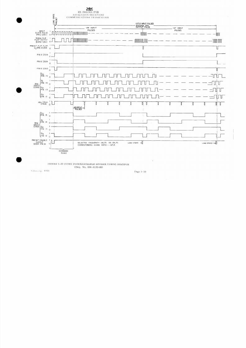
8/9/2019 KX 170A - Maintenance Manual Honeywell
http://slidepdf.com/reader/full/kx-170a-maintenance-manual-honeywell 459/586
128 INPUT
127.5 INPUT PULSES
AVERAGE PER
OUTPUT PULSE
127 INPUT
d
CLOCK PULSE
,,,;y;‘,,)
PULSES
- - - - - - - - - ll]l,,,,,l - - - - - - - - - -
llllll
50KHz FLIP I
FLOP OUTPUT
7J(PIN7130 1) 0) - - - - - - - -
PRESET FLIP FLOP ’
Q2(PIN IO1300 o
PIN 9 1309
u
u
I
,
I
PIN 6 1309
0
j
PIN 8 1303
u
-------
KHz 1304 ’
I
(PIN8) 0
u
u u u I.; II u
U
U U
U II u
i
Q3
I
PIN I2 o
PRESET ENABLE 1
OUT PUT
a304 PIN 6) o
I
I
I I I
SELECTED FREQUENCY 126.70 OR 135.70
LOAD STATE
CORRESPONDING DIVIDE RATIO-- 127.5
\’
V
J
FXPANDED
SCALE
FIGURE 5-22 COMM PROGRAMlKdBLE DIVIDER TIMING DLAGR4M
(Dwg. No. 696-6119-00)
;ic:h ‘b.4 ‘s ;, 1973
Page 5.55
-I-
A-

8/9/2019 KX 170A - Maintenance Manual Honeywell
http://slidepdf.com/reader/full/kx-170a-maintenance-manual-honeywell 460/586
COMM
1310
+I6
NAV
1210
400 KHz REF; FREQ. ’
PIN 14
0
200 KHz I
PIN I 8 12
0
100 KHz
PIN 9
50 KHz
PIN 8
25 KHz I
PIN I I
0
COUNTER OUTPUT l
1204,1304 PIN 6 0
1212, 1312
I
PIN 0
0
1212,1312
I
PIN 6
0
12 I I, 131 I
PIN 3
I
0
1211, 1311
I
PIN 6
0
12lI,13lI
I
PIN II
0
VOLTAGE T,RANS
LATOR OUTPUT
TP202, TP302
0
LOW PASS FILTER
OUTPUT
TP201, TP30l
FIGURE 5.
February, 973
KING
KX 170B/KX ;'75B
NAVIGATION RECEIVER/
COMMUNICATIONS TRANSCEIVER
A) PHASED LOCKED
APPROXIMATE WAVEFORMS
-I 25.00, 134.00
--+21.00. 130roo
--- --
--- -- -
m------
1
I
-- ---
---J-
IIu uu
1 I
I
I I
I1
PHASE ESTABLISHED TO GIVE PROPER VCO BIAS
-a.5v TO MAINTAIN PHASE LOCK
OV
DC DRIVES fVCO TO MAINTAIN PHASE LOCK
3 FRLXJ. & PHASE COMPARATOR TIMING DLAGRAM
(Dwg. No. 696-6120-00)
B) VCO FREQUENCY HIGH
C) VCO FREQUENCY LOW
(COUNTER FREQUENCY LOW)
(COUNTER FREQUENCY HIGH 1
m-----
iv-
>LTS
0 V( -TS
DC DRIVES fVr.., LOW
DC DRIVE S fVCO HIGH
Page 5-57
8.5V-
m-----
I
----
II u
u

8/9/2019 KX 170A - Maintenance Manual Honeywell
http://slidepdf.com/reader/full/kx-170a-maintenance-manual-honeywell 461/586

8/9/2019 KX 170A - Maintenance Manual Honeywell
http://slidepdf.com/reader/full/kx-170a-maintenance-manual-honeywell 462/586
KX 170B/KX 175B
NAVIGATION RECEIVER/
COMMUNICATIONS TRANSCEIVER
FIGURE 5-24 NAV BLOCK DIAGRAM
(Dwg. No. 696-6121-00)
Page 5-60
February, 1973

8/9/2019 KX 170A - Maintenance Manual Honeywell
http://slidepdf.com/reader/full/kx-170a-maintenance-manual-honeywell 463/586
SPEAKER
AUDIO
XMIT KEY
KlNG
KX 17OB/KX 175R
NAVIGATION RECEIVER/
COMMUNICATIONS TRANSCEIVER
1
I
I
8 13675MHz
VARACTOR
FILTER -
(2 POLE1
. RF AMP
t
VARACTOR
BALANCED
.
FILTER
. IST MIX
XTAL
- FILTER
. 2ndMIX
2 POLE
l FILTER
c
I. F AMP
(2 POLE)
9MHz
661 25KHz
T
T
t 1
LOW PASS I,
R-F
POWER AMP
SPEAKER
SIDETONE
REsisToR (OPTIONAL)
RECEIVER
DISABLE
AUDIO
OUTPUT -
AMPL.
*
HEADPHONE/
SIDETONE
REGULATORS
MIKE INPUT
AUXILIARY
AUDIO
INPUTS
- .~
I
FIGURE 5-25 COMM BLOCK DIAGRAM
I
(Dwg. No. 696-6122-00)
NOISE LIMITER
c
NOISE AMP
AND FILTER
SOUELCH -
DISABLE
AUDIO AMP
CI
February, 1973
Page 5-61

8/9/2019 KX 170A - Maintenance Manual Honeywell
http://slidepdf.com/reader/full/kx-170a-maintenance-manual-honeywell 464/586
(KY 195B)
FIGURE 5-26 COMM BOAR D ASSEMBL1
(Dwg. No. 300-0653-00 Rev. 1)
February, lij’i‘3
Page 5-63

8/9/2019 KX 170A - Maintenance Manual Honeywell
http://slidepdf.com/reader/full/kx-170a-maintenance-manual-honeywell 465/586

8/9/2019 KX 170A - Maintenance Manual Honeywell
http://slidepdf.com/reader/full/kx-170a-maintenance-manual-honeywell 466/586

8/9/2019 KX 170A - Maintenance Manual Honeywell
http://slidepdf.com/reader/full/kx-170a-maintenance-manual-honeywell 467/586

8/9/2019 KX 170A - Maintenance Manual Honeywell
http://slidepdf.com/reader/full/kx-170a-maintenance-manual-honeywell 468/586

8/9/2019 KX 170A - Maintenance Manual Honeywell
http://slidepdf.com/reader/full/kx-170a-maintenance-manual-honeywell 469/586

8/9/2019 KX 170A - Maintenance Manual Honeywell
http://slidepdf.com/reader/full/kx-170a-maintenance-manual-honeywell 470/586

8/9/2019 KX 170A - Maintenance Manual Honeywell
http://slidepdf.com/reader/full/kx-170a-maintenance-manual-honeywell 471/586

8/9/2019 KX 170A - Maintenance Manual Honeywell
http://slidepdf.com/reader/full/kx-170a-maintenance-manual-honeywell 472/586
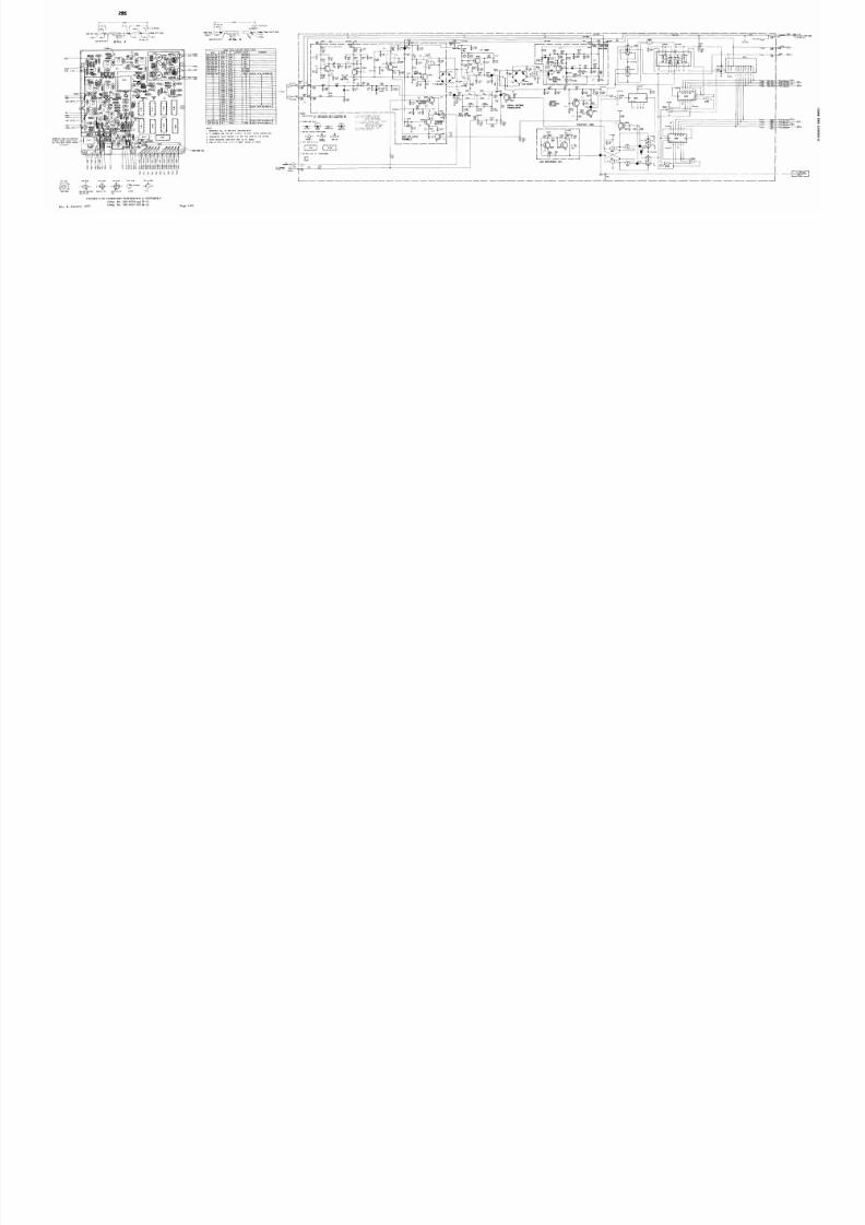
8/9/2019 KX 170A - Maintenance Manual Honeywell
http://slidepdf.com/reader/full/kx-170a-maintenance-manual-honeywell 473/586

8/9/2019 KX 170A - Maintenance Manual Honeywell
http://slidepdf.com/reader/full/kx-170a-maintenance-manual-honeywell 474/586

8/9/2019 KX 170A - Maintenance Manual Honeywell
http://slidepdf.com/reader/full/kx-170a-maintenance-manual-honeywell 475/586

8/9/2019 KX 170A - Maintenance Manual Honeywell
http://slidepdf.com/reader/full/kx-170a-maintenance-manual-honeywell 476/586

8/9/2019 KX 170A - Maintenance Manual Honeywell
http://slidepdf.com/reader/full/kx-170a-maintenance-manual-honeywell 477/586

8/9/2019 KX 170A - Maintenance Manual Honeywell
http://slidepdf.com/reader/full/kx-170a-maintenance-manual-honeywell 478/586

8/9/2019 KX 170A - Maintenance Manual Honeywell
http://slidepdf.com/reader/full/kx-170a-maintenance-manual-honeywell 479/586

8/9/2019 KX 170A - Maintenance Manual Honeywell
http://slidepdf.com/reader/full/kx-170a-maintenance-manual-honeywell 480/586
R4
R4
R4
RL
KING RADIO CORl? PARTS LISTING
SYMBOL PART NUMBER
069-1019-00
069-1020-00
069-1021-00
008-0004-00
008-0005-03
012-1006-00
016-1015-00
016-1038-00
035-1013-04
047-1695-00
047-1728-01
047-1729-01
047-1730-02
047-1731-02
047-1737-01
047-1943-00
047-2267-02
047-2268-01
047-2269-01
047-2293-01
047-2338-01
047-2496-01
047-2623-01
057-1443-01
057-1447-01
057-1448-01
076-0339-00
089-2105-22
089-2140-00
089-5899-04
089-5903-04
089-6008-03
089-6008-04
089-6167-05
089-6258-04
089-7018-04
091-0118-03
091-0118-04
091-0118-05
091-0118-06
091-0169-00
150-0020-10
187-1011-00
DESCRIPTION
KX 175B
KX 170B
KY 195B
Solder Lug
Lug
Nyl Lacing Cord
Adhesive
Spray Adhesive #77
Plstc Bag 9 x 18
Cover, Equip _c
Cover COMM SMO
Cover P. A.
Rail Left Side
Rail Right Side
Cover NAV SMO
Spring Cup
Cover Bottom
Shield Pad (Mixer)
Shield Pad (0s~)
Shield Pad (RF)
Cover Top
Shield Pad NAV IF
Shield Pad COMM IF
Serial Number Tag
Serial Number Tag
Serial Number Tag
Spacer
Nut #4 Speed
Nut Esna
Scr 2-56 x l/4 PHP
Scr 4-40 x l/4 PHP
Scr 4-40 x 3/16 FHP
Scr 4-40 x l/4 FHP
Scr 6-32 x 5/16 FHP
Scr 4-24 x l/4 FHP
Scr 4-40 x l/4 THP
Insulator
Insulator
Insulator
Insulator
Insulator
Shrink Tubing
Liner Rubber
00-0076-0077-001
QUANTITY
1
2
iR
iR
m
1
1
1
1
1
1
1
1
1
2
1
1
1
1
1
1
6
8
2
4
7
.O
2
4
8
7
2
1
1
1
1
2
4
1
2
,R
iR
IR
1
1
1
1
1
1
1
1
1
2
1
1
1
1
1
1
6
8
2
4
7
10
12
4
8
?
:
. :
L
X
1
2
LR
LR
LR
1
1
1
1
1
1
1
1
1
6
8
2
4
7
8
12
4
8
7
1
Rev. 4, January, 1976
Page 6-l
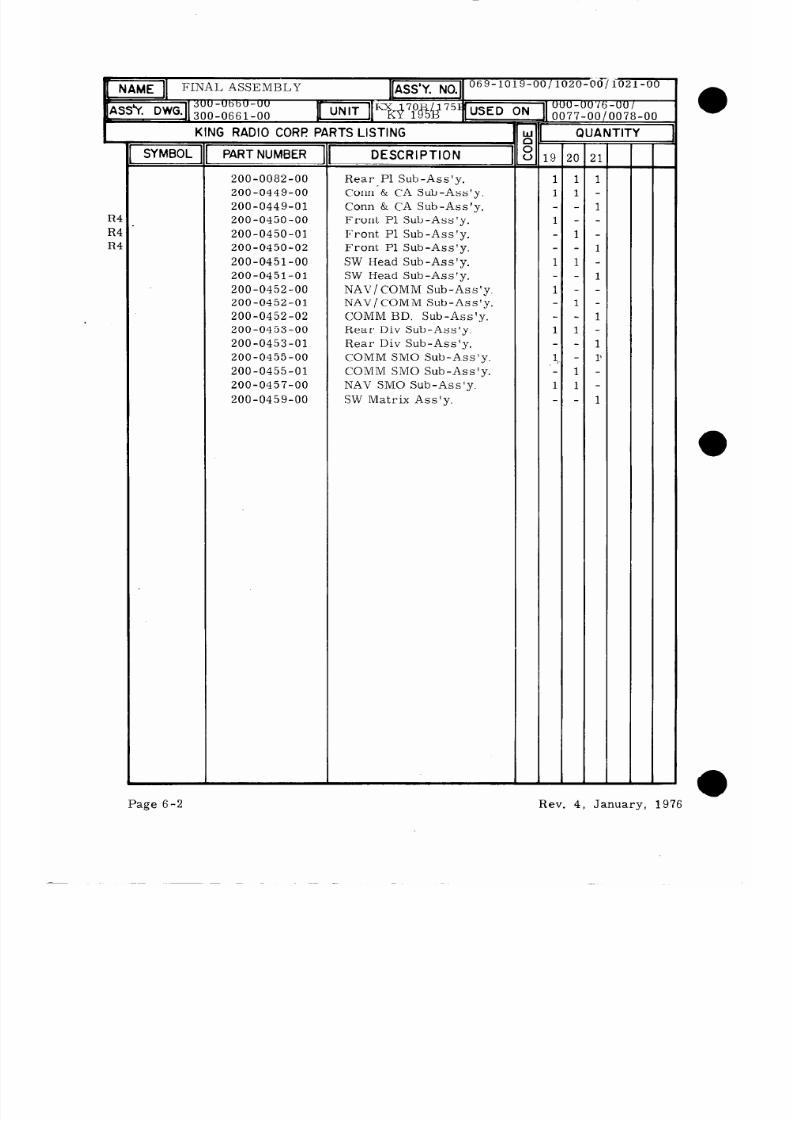
8/9/2019 KX 170A - Maintenance Manual Honeywell
http://slidepdf.com/reader/full/kx-170a-maintenance-manual-honeywell 481/586
FINAL ASSEMBLY
300-0661-00
KING RADIO CORF PARTS LISTING
SYMBOL
R4
R4
R4
Page 6-2
Rev. 4, January,
PART NUMBER
200-0082-00
Rear-P1 Sub-Ass’y.
200-0449-00
Conn & CA Sub-Ass’y.
200-0449-01
Conn & CA Sub-Ass’y.
200-0450-00 Front Pl Sub-Ass’y.
200-0450-01 Front Pl Sub-Ass’y.
200-0450-02
Front Pl Sub-Ass’y.
200-0451-00
SW Head Sub-Ass’y.
200-0451-01 SW Head Sub-Ass’y.
200-0452-00
NAV/ COMM Sub-Ass’y.
200-0452-01
NAV/COMM Sub-Ass’y.
200-0452-02 COMM BD. Sub-Ass’y.
200-0453-00
Rear Div Sub-Ass’y.
200-0453-01
Rear Div Sub-Ass’y.
200-0455-00
COMM SMO Sub-Ass’y.
200-0455-01
COMM SMO Sub-Ass’y.
200-0457-00 NAV SMO Sub-Ass’y.
200-0459-00
SW Matrix Ass’y.
DESCRIPTION
uuu UU’lb: uo/
007;-OO/iO78-00
QUANTITY
=
-
1976

8/9/2019 KX 170A - Maintenance Manual Honeywell
http://slidepdf.com/reader/full/kx-170a-maintenance-manual-honeywell 482/586
KlNG
KX 170B/KX 175B
NAVIGATION RECEIVER /
COMMUNICATIONS TRANSCEIVER
1 [
9 --
E
4
I$ B
\
\ 089-6/67-05(Z)
01/7-/730-02
og9-6~~58- 04f4)
@9-Em9-03cq
Rev. 4, JanuarjT, 1976
089-5903-W(4)
I- 02
(70
~&+600&03(Z)
NO-E-5
/. RrF0?E/VCE B/M
2. OU/EN?- KHz GEAR
S/DE, TOP UP, SO T//AT
POS/T//oN ON PLATE PR/OR TO ASS&MBLY.
THE Mh’cs GEi4fi C+=?IVE OAJ /vAV. SIDE, A5 VIEWED FROM BACI: ‘SlDE,T~L
SW-L BE AGAIAIST STOP AT
M O 51 C LO C KWI SE P O SI Tl OU .
THE COM
Mtk GEARS’ P05lTION UO-/- CRITIC4L.
M Y- 61 4 7 -0 5( Z)
i(
ms-5903-04
059 - 6259-op
( 4)
FIGURE
6 -
1 FINAL
ASSEMBLY
(Dwg. No. 300-0660-OO)(Sht. 1 of 2) (Rev 5)
Page 6-3

8/9/2019 KX 170A - Maintenance Manual Honeywell
http://slidepdf.com/reader/full/kx-170a-maintenance-manual-honeywell 483/586
KlNG
I% 170B/KX 175B
NAVIGATION RECEIVER/
COMMUNICATIONS TRANSCEIVER
1” ,:j
l/J ’ .I’ 1
zoo-,78‘%0fku75,9)
‘ZOO- I lS6& -0//K//708)
; :
1.1
r
1
ZM - 045/-00
,, 076~QiWFC’O (6)
/
0 47 - Z i? 9 3# /
09/-O//8-05 .
DETA/L %I*
-- &J-0457- a3
04/T-/73--o/
09/-O//8 -03 Q 1
OY7-2268-O/(Z).
D ET A/ L J 44 *
\
5ZwO RECE/YFL
//4&C T/O/V ACCESS
,&P- 6-43 ( 2)
\
089-5899 -0 4Cz
k.
09/-O/69
.oo ’
OYZ-2623-01
DETaIL I”
f FULL SOLDER
-SEAM
s
ALOIVG EDGE (12 PLCSJ
/zoo-0453 00
A
/2?00 -0~+5--M
ZOO-0445-O/ (KX/700
0
.
,/”
04’72269-O/ (2)$
09/ -O//B -04 (2)
,0 89- b oo0- 0 3( b)
,* oq7- /729-o/
FIGURE 6 - 1A FINAL ASSEMBLY
(Dwg. No.
300-0660-OQ(Sht. Zof 2)(R-5)
Page 6-3A
Rev. 4, January, 1976

8/9/2019 KX 170A - Maintenance Manual Honeywell
http://slidepdf.com/reader/full/kx-170a-maintenance-manual-honeywell 484/586
089-5903 -0q
0
057-/537 -01
K Y l9 5 BE O NL Y .
zoo -oiwz-00
089-5903-W(4)
1, \
\ ix
‘, l
1 ‘\
006 -0005
/50-0020-/O
089-6&%03(Z)
NO-I-E5
/. RFF&UENCE L$& 569 -/GE’/ -00 (KY/95B)
2. omwr KHr Gm? ~7mc.s~o~ FACE PLATE .~SSY AS V/EWEL~ FUOM BAL
SIDE, TOP UP, 50 V/MT HOAS’ /N GFARS /d//V THE /Z 85 O’CLOCK
POS/T/ON ON PLATE PRIOR TO ASSEMBLY.
MHt GEARS’ POS/T/ON NOT CRITICAL.
01/7-2267-02
m9-5903~oq
099 - 6ZB-of ( 4)
Rev. 4, January, 1976
FIGURE 6 -2 FINAL ASSEMBLY
(Dwg. No.
300 -066 l-00)( Sht. 1 of 2) (R-5)
Page 6-3B

8/9/2019 KX 170A - Maintenance Manual Honeywell
http://slidepdf.com/reader/full/kx-170a-maintenance-manual-honeywell 485/586
KlNG
KY 195B
NAVIGATION RECEIVER /
COMMUNICATIONS TRANSCEIVER
A
I
I
I
m
quououuuuuo Q uuuuuuuuuu
q
6
//-ass - 2@5-22 (4)
ass-rols-/ (7)
4
9
Q
._ _
/
/’
/’
. za6 -045/-o/
I’
49/-o/ M-L73
OW2266-O/
DEW/L w
*FULL SOLDER SEA/Y
ALONG EDGE (4 PLCX) .
,-ZOO-0453-01
,OB9- bC~8- 03(4)
/0474729*
I
I
1
047-/943-00
OSS-59A?dp’
CEMENT /
SULArD
swsu?
TTH ox-
AL/GN HOLES
Rev. 4. January, 1976
FIGURE 6 -2A FINAL ASSEMBLY
(Dwg. No. 300-0661-OO)(Sht. 2 of Z)(R-5)
Page 6-3C

8/9/2019 KX 170A - Maintenance Manual Honeywell
http://slidepdf.com/reader/full/kx-170a-maintenance-manual-honeywell 486/586
Parts List Revisions Record
Assembly No. 066-1019-00/1020-00/1021-00 (B/MRL Rev 15)
Manual Revision No. 4
ACTION
SYMBOL PART NUMBER
DESCRIPTION
QUANTITY
CHANGE 047-2269-01
CHANGE 091-0118-04
DELETED
016-1038-00
ADDED
026-0005-00
CHANGE
047-2338-02
ADDED
091-0109-00
CHANGE
200-1786-00
CHANGE
200-1786-01
CHANGE 200-1786-02
Shield Pad (OS c) 22-
Insulator
22 -
Wire, #18 Buss .l. 1. 1
Cover. Top 1 1 1
Plastic Ties 14 14 14
Front Plate Sub-Ass’y 1 - -
Front Plate Sub-Ass’y - 1 -
Front Plate Sub-Ass’y - - 1
Rev. 4, January, 1976
Page 6-3D

8/9/2019 KX 170A - Maintenance Manual Honeywell
http://slidepdf.com/reader/full/kx-170a-maintenance-manual-honeywell 487/586
R4
R4
R4
R4
R4
R4
R4
R4
R4
R4
R4
R4
R4
R4
R4
SYMBOL
PART NUMBER
200-0450-00
200-0450-01
200-0450-02
KING RADIO CORf? PARTS LISTING
008-0005-03
008-0040-00
016-1008-04
016-1016-00
016-1033-00
016-1034-00
026-0001-00
026-0005-00
029-0096-01
029-0096-02
029-0097-01
047-1672-00
047-1713-00
047-2214-01
047-2613-00
047-2630-00
047-2631-00
047-2632-00
047-2634-00
047-2638-01
057-1369-00
057-1415-00
073-0053-00
073-0085-00
073-0123-01
073-0195-04
073-0195-05
078-0024-00
088-0125-00
088-0141-00
088-0326-01
089-2106-30
089-5569-03
089-5874-03
089-5899-02
089-6218-04
089-6222-04
089-8023-30
089-8042-30
089-8184-00
L
I DESCRIPTION
SSv. DWG.11
300-0648-00
L UN
KX 175B
KX 170B
KX 195B
Lug
Lug Solder
Glyptal Blue
Lubricant
ADH Activator
Adhesive
#26 Buss Wire
#18 Buss Wire
Gear Drive MHz
Gear Drive MHz
Gear Drive KHz
Spring Detent
Spring SW Detent
Stop Arm
Insr Fr Pnl Comm
Insr Fr Pnl NAV
Insr Fr Pnl Comm A
Insr Fr Pnl Comm B
Insr Fr Pnl NAV
Clamp Hold Down
Logo
Logo Tag Blk
Knob KHz
Knob Mode Vol
Knob MHg
Pnl Fr Xcur
Pnl Fr
Spring Cprsn
Hold Down Unit
Lever SW
Lens
Hex Nut l/4-32
#2-56 THP
Scr 2-56 x 3/16PHP
Scr 2-56 x 1/8PHP
Sscr #4-40
Sscr #6-32
Washer Flat
l/4” Int T Lk Wash
Wash Spacer
1
1
2
2
2
8
1
4
4
8
4
2
1
1
1
2
2
2
8
1
4 I
1
2
8
6
1
1
A
-
Rev. 4, January, 1976
1
1
AF
AF
AF
AF
.4
1
1
1
2
2
2
1
1
8
1
JANTITY
X
1
1
8
X
1
2
2
2
2
1.
1
1
6
1
2
1
2
-
Page 6-4
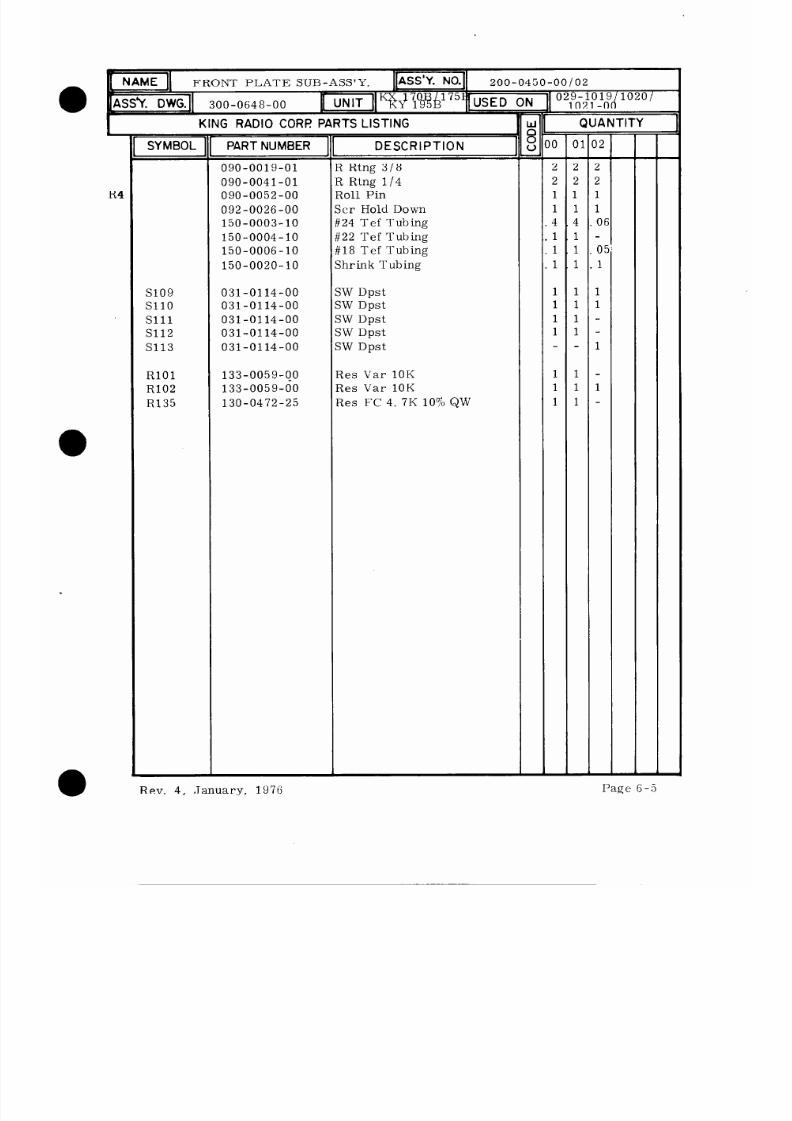
8/9/2019 KX 170A - Maintenance Manual Honeywell
http://slidepdf.com/reader/full/kx-170a-maintenance-manual-honeywell 488/586
t
AME
FRONT PLATE SUB-ASS’Y. 200-0450-00102
ASS’Y. DWG.
300-0648-00
[ UNIT j1%3J”&Q75z[~~ED 0~
1
KING RADIO CORI? PARTS LISTING
II
QUANTITY
SYMBOL 1
PART NUMBER
DESCRIPTION
=
IO
z
2
1
1
4
1
1
1
1
1
1
1
1
1
1
T
T
2
1
1
0t
OE
1
1
1
1
1
E
z-
2
1
1
4
1
1
1
1
1
1
1
1
1
1
=
-
R4
090-0019-01 3 Rtng 318
090-0041-01
3 Rtng l/4
090-0052-00 3011 Pin
092-0026-00 jcr Hold Down
150-0003-10 /24 Tef Tubing
150-0004-10
f22 Tef Tubing
150-0006-10
f18 Tef Tubing
150-0020-10
jhrink Tubing
s109
031-0114-00 :W Dpst
SllO
031-0114-00 ?W Dpst
Sill
031-0114-00 :W Dpst
s112
031-0114-00
$W Dpst
s113
031-0114-00
SW Dpst
RlOl
133-0059-00
3es Var 10K
R102
133-0059-00
Res Var 10K
R135
130-0472-25 Res FC 4. 7K 10% QW
-
-
=
Rev. 4, January, 1976
Page 6-3

8/9/2019 KX 170A - Maintenance Manual Honeywell
http://slidepdf.com/reader/full/kx-170a-maintenance-manual-honeywell 489/586
Parts List Revisions Record
Assembly No, 200-0450-00/02 (B/MRL Rev 15)
Manual R.evision No. 4
ACTION SYMBOL PART NUMBER DESCRIPTION
QUANT IT Y
CHANGE 026-0004-00
#20 Buss Wire
CHANGE 029-0097-03
Gear, Drive KHz
CHANGE 047-1706-01
Insr Fr Pnl Comm
CHANGE
047-2361-00 Insr Fr Pnl Comm A
CHANGE 047-2358-01
Ins r Fr Pnl NAV
CHANGE 047-2342-01 Insr Fr Pnl NAV
CHANGE 073-0143-02
Pnl Fr Xcur
CHANGE
073-0153-02
Pnl Fr
ADDED 147-0019-01
Bushing
ADDED 016-1045-00 Silicone Seal
ADDED 047-.1708-00
Frame Lens
CHANGE
089-5569-03 #2-56 THP
CHANGE
047-2638-01
Clamp, Hold Down
ADDED 047-2638-02 Clamp Hold Down
ADDED 080-6004-03
#2-56 x 3116 FHP
CHANGE 150-0003-10
#24 Teflon Tubing
CHANGE 090-0052-02
Roll Pin
CHANGE
047-2214-00
Stop Arm
CHANGE 029-0096-03
Gear Drive MHz
CHANGE 073-0053-04 Knob KHz
CHANGE 073-0123-03 Knob MHz
CHANGE
029-0096-04 Gear Drive MHz
ADDED 091-0018-02
Washer
Page 6-6
.l .l .06
2 2 2
11 -
- -
1
1 -
1 - -
1 1 -
- -
1
2 2 2
AR AR AR
2 2 2
6 6 7
6 6 5
2 2 1
2 2 1
.3.3 -
1 1 1
- -
1
1 1 -
2 2 2
2 2 2
1 1 2
2 2 2
Rev. 4, January, 1976
l

8/9/2019 KX 170A - Maintenance Manual Honeywell
http://slidepdf.com/reader/full/kx-170a-maintenance-manual-honeywell 490/586
KING
la 170B/Kx 175x3
NAVIGATION RECEIVER/
COMMUNICATIONS TRANSCEIVER
089-5569-03(2)
-089-8023-30(2l
/
029-0097-03
091-0018-02 (2)
029-0096-04
029-0096-03 KX 1708/1758)
029-0096-04:KY 1958)
047-26
--. “. \
3&o,<K.m-x
031-0114-00 (KX 1708/1758
.
- 7
/
08%5569-03(5)
,4,,,,‘,, f&i,,
I
2
3.
4.
5.
6.
090-0019-Ol(2)
NOTES:
RIOI AND ITS RELATED HARDWARE ARE NOT ON KY 195.
ALL SCREWS AND NUTS NOT SECURED BY LOCKWASHER SHALL BE
LIQUID STAKED USING BLUE GLY PTAL. (016-1008-04)
THIS FACE PLATE ASSEMBLY IS FOR:
S/N 35000 & BELOW KX170B
S/N 16500 & BELOW KX175B
S/N 5700 & BELOW KY195B
d47- 17OB-OO(2)
FACE PLATE ASSEMBLY MAY BE ORDERED UNDER ONE OF
THE FOLLOWING NUMBERS:
KX 1758 -2oo- 0450-00
KX l70B- 200-b450-0 I
KY 195B-
200-0450- 0 2
lGURE 6-3 FRONT PLATE ASSEMBLY
(Dwg. No. 300-0648-OO)(Sht. 1 of 2)(R-12)
Rev. 4, January, 1976 Page 6-7
‘t.
&I :.:...,
” ‘,
J
047-2360-o I (KY
NOTE 5
-089-6222-04(e)
089-6218 -04(4)
(KY 1958 (2)

8/9/2019 KX 170A - Maintenance Manual Honeywell
http://slidepdf.com/reader/full/kx-170a-maintenance-manual-honeywell 491/586
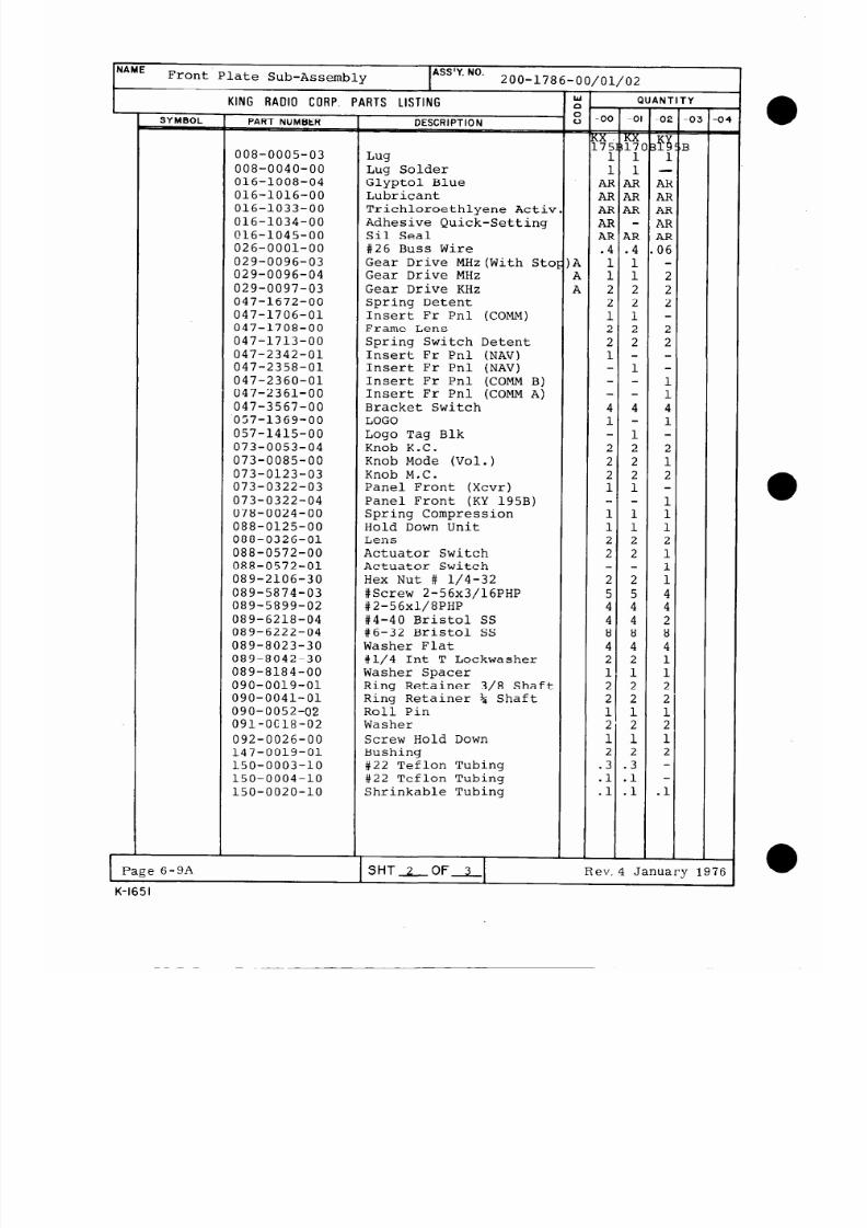
8/9/2019 KX 170A - Maintenance Manual Honeywell
http://slidepdf.com/reader/full/kx-170a-maintenance-manual-honeywell 492/586
I-
r-
NAME
FrontPlate Sub-Assembly
ASS’Y. NO.
200-1786-00/01/02
KING RADIO CORP. PARTS LISTING
SYMBOL
, -I
PART NUMBER
-
DESCRIPTION
-
008-0005-03
Lug
008-0040-00
Lug Solder
016-1008-04
Glyptol Blue
016-1016-00
Lubricant
016-1033-00
Trichloroethlyene Activ
016-1034-00
Adhesive Quick-Setting
016-1045-00
Sil Seal
026-0001-00 #26 Buss Wire
029-0096-03
Gear Drive MHz(With Sto
029-0096-04 Gear Drive MHz
029-0097-03
Gear Drive KHz
047-1672-00
Spring Detent
047-1706-01
Insert Fr Pnl (COMM)
047-1708-00
Frame Lens
047-1713-00
Spring Switch Detent
047-2342-01
Insert Fr Pnl (NAV)
047-2358-01 Insert Fr Pnl (NAV)
047-2360-01
Insert Fr Pnl (COMM B)
047-2361-00
Insert Fr Pnl (COMM A)
047-3567-00
Bracket Switch
057-1369-00
LOGO
057-1415-00
Logo Tag Blk
073-0053-04 Knob K.C.
073-0085-00 Knob Mode (Vol.)
073-0123-03
Knob M.C.
073-0322-03
Panel Front (Xcvr)
073-0322-04
Panel Front (KY 195B)
078-0024-00
Spring Compression
088-0125-00
Hold Down Unit
088-0326-01
Lens
088-0572-00
Actuator Switch
088-0572-01 Actuator Switch
089-2106-30
Hex Nut # l/4-32
089-5874-03 #Screw 2-56~3/16PHP
089-5899-02 #2-56~1/8PHP
089-6218-04
#4-40 Bristol SS
089-6222-04 #6-32 Bristol SS
089-8023-30
Washer Flat
089-8042-30 #l/4 Int T Lockwasher
089-8184-00
Washer Spacer
090-0019-01
Ring Retainer 3/8 Shaft
090-0041-01 Ring Retainer % Shaft
090-0052-02
Roll Pin
091-OE18-02
Washer
092-0026-00 Screw Hold Down
147-0019-01
Bushing
150-0003-10
#22 Teflon Tubing
150-0004-10
#22 Teflon Tubing
150-0020-10
Shrinkable Tubing
w
8
0
A
A
A
-
-00
F
\X
-7i
1
AF
AF
AF
AF
AB
.4
1
1
2
2
1
2
2
1
C
-
-01
q
1
AR
AR
AR
AR
4
'1
1
2
2
1
2
2
Page 6-9A
K-1651
SHT-OF-1
4
1
1
1
2
2
2
5
4
4
8
4
2
1
2
2
1
2
1
i
.z
1
:I
1
4
2
5
4
4
8
4
2
1
2
2
1
2
1
2
3
:1
4Nl
-
-02
FE
1
AH
AR
AR
AR
AR
06
2
2
2
2
2
2
1
2
1
1
1
2
1
1
1
4
4
2
8
4
1
1
2
2
1
2
1
2
Rev.4 January 1976
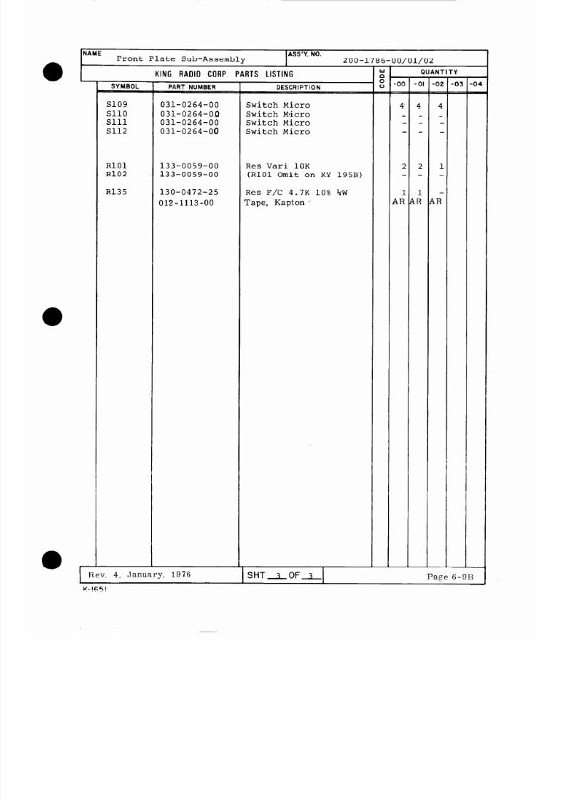
8/9/2019 KX 170A - Maintenance Manual Honeywell
http://slidepdf.com/reader/full/kx-170a-maintenance-manual-honeywell 493/586
)0/01/02
NAME
Front Plate Sub-Assembly
ASS’Y. NO.
200-1786-c
KING RADIO CORP. PARTS LISTING
T
I
SYMBOL T
PART NUMBER
,
DESCRIPTION
-
-
l l
0
0
-
-00
=
4
2
1
9R
Q
-
-01
-
4
2
1
LR
\Nl
-
-02
-
4
1
\R
s109
SllO
Sill
s112
RlOl
R102
R135
031-0264-00
031-0264-00
031-0264-00
031-0264-00
133-0059-00
133-0059-00
130-0472-25
012-1113-00
I
Rev. 4, January, 1976
1 SHT-LWLI
Switch Micro
Switch Mkro
Switch Micro
Switch Micro
Res Vari 10K
(RlOl Omit on KY 195B)
Res F/C 4.7K 10% %W
Tape, Kapton
-
‘Y
-
-03
=
Page 6-9B

8/9/2019 KX 170A - Maintenance Manual Honeywell
http://slidepdf.com/reader/full/kx-170a-maintenance-manual-honeywell 494/586
'300-1786-00
Page 6-9C
1 SHT-LOF? 1
Rev. 4, January, 1976
K-1650 3/73
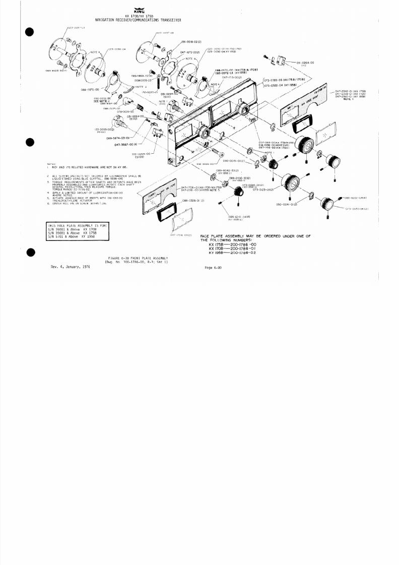
8/9/2019 KX 170A - Maintenance Manual Honeywell
http://slidepdf.com/reader/full/kx-170a-maintenance-manual-honeywell 495/586
NAVIGATI
KING
KX 170B/KX 175B
ON RECEIVER/COMMUNICATI3NSTRANSCEIVER
,i
029-0097-03
m
,091-0018-02 (2)
/029-0097-03
029-0096-04
029-0096-03 KXl70B/l75B)
029-0096-04:KY 1958)
- 031-0264-00
089-8023-30
OB&O572-00 (KXl75B a 17OB)
0138-0572-01 (KY 195B)
047-1713-OO(2)
000-05~2-00
090-0052-02’ w/-A
SEE NOTE 6
-----
047-2342-o
047-2350-0
\
047-2360 -0
NOTE
‘I (KX
I (KX
I (KY
5
000-0125-00
078-0024-00
(Rl02)
047-3567-00 (4) 1
\
57-1415-00 (KX-170B)
l
031-0264-00
\
(slog)
090-0019-Ol(2)
NOTES’
I
RIOI AND ITS RELATED HARDWARE ARE NOT ON KY 195.
2
ALL SCREWS AND NUTS NOT SECURED BY LOCKWASHER SHALL B E
LIQUID STAKED USING BLUE GLYPTAL. tOI&1008-04)
‘\
089-8042 -3Oi2)
b
,
‘r-7-
/ (KY 1958 (1)
8 ,089-2106’-30(2)
3. TOROUE REQUIREMENTS AFTER SHAFTS AND DETENTS HAVE BEEN
/
A+@-1
(KY 1958(l)
.047-1706-01 (KX I70B/KX 1758)
047-2361-00 (KYl95B) NOTE 5
.073-0005-00~2)
073-Ol23-03(2)
\
PROPERLY ASSEMBLED AND LUBRICATED, ROTATE EACH SHAFT
SEVERAL REVOLUTIONS. THEN MEASURE TORQUE.
TORQUE RANGE: 22-30 IN;OZ.
/”
4
APPLY A LIMITED AMOUNT OF LUBRICANT(016-1016-00)
WHERE NOTED.
5
ACTIVATE ADHESIVE BACK OF INKRTS WITH 016-1033-00
6222-04(a
,088-C326-01 (21
^̂ ^ ^̂
TRICHLOROETHYLENE ACTIVATOR
I-K.
6. CENTER ROLL PIN ON SCREW WITHIN f.016.
t
1
‘oes-6218 -04(4)
(KY 1958 (2)
I
HIS FACE PLATE ASSEMBLY S FOR:
S/N 35001 & Above KX 170B
I
S/N 35001 & Above KX 175B
S/N 5701 & Above KY 195B
047.1708.OO(21
FACE PLATE ASSEMBLY MAY BE ORDE RED UNDER ONE OF
THE FOLLOWING NUMBERS:
KX 175B -2oo- ,I’786 -00
KX 17OB-
200-
I
786-01
KY 195B-
200-
I
786- 02
Rev. 4, January, 1976
FIGURE 6-3B FRONT PLATE ASSEMBLY
(Dwg. No. 300-1786-00, R-3; Sht 1)
Page 6-9D

8/9/2019 KX 170A - Maintenance Manual Honeywell
http://slidepdf.com/reader/full/kx-170a-maintenance-manual-honeywell 496/586
KlNG
KX 17OB/kX 1758
NAVIGATION RECEIVER/COMMUNCIATIONS RANSCEIVER
KY 195B
FIGURE 6-3C FRONT PLATE ASSEMBLY
(Owg. No. 300-1786-00, R-3, Sht 2)
Rev. 4, January, 1976
Page 6-9E

8/9/2019 KX 170A - Maintenance Manual Honeywell
http://slidepdf.com/reader/full/kx-170a-maintenance-manual-honeywell 497/586
KING RADIO CORI? PARTS LISTING
sVMBoL
Page 6-10
February, 1973
PART NUMBER 1
200-0451-00
200-0451-01
008-0001-01
008-0005-03
016-1004-00
016-1008-04
016-1016-00
025-0018-00
025-0018-04
025-0018-09
025-0018-11
025-0018-14
025-0018-15
025-0018-18
025-0018-19
025-0018-24
025-0018-26
025-0018-28
025-0018-29
025-0018-30
025-0018-34
025-0018-36
025-0018-39
025-0018-40
025-0018-44
025-0018-49
025-0018-51
025-0018-54
025-0018-59
025-0018-64
025-0018-66
025-0018-69
025-0018-74
025-0018-79
025-0018-84
025-0018-88
025-0018-89
025-0018-90
025-0018-91
025-0018-92
025-0018-93
025-0018-95
025-0018-96
DESCRIPTION
I
1
KX 170B/KX 175B
KY 195B
Solder Lug
Lug
T hrm Compound
Glyptal Blue
Lubricant
Wire #26
Wire #26
Wire #26
Wire #26
Wire #26
Wire #26
Wire #26
Wire #26
Wire #26
Wire #26
Wire #26
Wire #26
Wire #26
Wire #26
Wire #26
Wire #26
Wire #26
Wire #26
Wire #26
Wire #26
Wire #26
Wire #26
Wire #26
Wire #26
Wire #26
Wire #26
Wire #26
Wire #26
Wire #26
Wire #26
Wire #26
Wire #26
Wire #26
Wire #26
Wire #26
Wire #26
Blk
Blk/ Ye1
Blk/ Wht
Brn
Brn/Yel
Brn/Grn
Brn/Gry
Brn/Wht
Red/ Ye1
Red/Blu
Red/Gry
Red / Wht
Orn/Blk
Orn/ Ye1
Orn/ Blu
Orn/ Wht
Yel/Blk
Ye1
Yel/ Wht
Grn/Brn
G rn/ Ye1
Grn/Wh,t
Blu/ Ye1
Blu
Blu/ Wht
Via/ Ye1
Iiio/ Wht
G ry/ Ye1
Gry
Gry/ Wht
Wht/Blk
Wht/Brn
Wht / Red
Wht/Orn
Wht/Grn
Wht/Blu
I
QUANTITY
2 2
5 5
JR AR
IR AR
JR AR
1.1 .4
1.0 -
1. 01. 0
- .6
1.0 -
- 1.0
- 1.0
1. 01. 0
1.0 -
- .8
- 1.0
1. 01. 0
1. 0
1. 01. 0
- 1.0
1.0 -
.6 -
1.0 -
- 1.0,
- 1.0
1.0 -
1. 01. 0
1.0 -
- 1.0
1. 01. 0
1.0 -
1. 01. 0
1.0 -
1.0.7
1. 01. 0
1. 61. 0
- 1.0
- 1.0
- 1.0
- 1.0
- 1.0

8/9/2019 KX 170A - Maintenance Manual Honeywell
http://slidepdf.com/reader/full/kx-170a-maintenance-manual-honeywell 498/586
R4
R4
R4
R4
R4
R4
R4
R4
R4
SYMBOL/
KING RADIO CORF PARTS LISTING
PART NUMBER
025-0018-97
025-0018-98
026-0001-00
047-1675-01
047-2619-00
047-2620-00
047-2621-00
047-2624-01
047-2624-02
047-2625-o 1
047-2635-00
076-0298-01
076-0298-03
076-0298-07
076-0298-08
076-0299-00
088-0136-00
088-0321-01
088-0232-01
089-2005-37
089-2076-30
089-2140-00
089-5381-16
089-5381-20
089-5857-04
089-6024-04
089-5903-05
089-8003-34
089-8023-30
089-8025-30
089-8100-30
089-8103-30
090-0019-01
091-0015-00
091-0015-11
091-0068-04
150-0003-10
150-0005-10
150-0020-10
200-0576 -00
200-0576-01
200-0576-02
200-0576-03
Rev. 4, January, 1976 Page 6-
1
DESCRIPTION
Wire #26
Wire #26
Wht / Via
Wht/Gry
Buss Wire #26
Support Dial
Brkt SW
Brkt SW
Erkt SW
Plate Dial YVItg
Plate Dial Mtg
Plate Transfer
Plate Xfr Adjust
Spacer. 218 Lg
Spacer . 281 Lg
Spacer . 156 Lg
Spacer . 110 Lg
Collar
Filter Blu Lamp
Cntr Whl 25KHz
Xfr Gear Cntr
Nut Hex #2-56
Nut #4-40
Nut Hex S/L #4-40
Mscr #2-56 x 1
Mscr #2-56 x 1 l/4
Sscr 4-40 x l/8
Scr 4-40 x l/4 SCH Cap
Scr 4-40 x 5/ 16 PHP
Lk Wash SR #4
Flat Wash
Wash #4
Flat Wash 3/8”
Flat Wash l/4”
Rtng Ring 3/8”
Grommet
Grommet
Wash Shoulder
#24 Tef Tubing
#20 Tef Tubing
Shrink Tubing
Comm MHz Whl Ass’y
Comm KHz Whl Ass’y
NA\: MHz Whl Ass’y
NAV KHz Whl Ass’y
O z-
/1020/
QUANTITY
.8
1
1
1
6
4
2
2
1
2
1
1
4
2
6
2
2
2
1
2
2
4
3
1
2
1
1
2
2
5
2
6
1
1
1
1
.4
1
1
1
1
2
2
4
4
2
1
1
4
3
2
4
2
1
2
1
.5
.3
.6
2
2
=
-

8/9/2019 KX 170A - Maintenance Manual Honeywell
http://slidepdf.com/reader/full/kx-170a-maintenance-manual-honeywell 499/586
NAME 11 SWITCHING HD.
SUB-ASS’Y
ILASS’Y. NO.1
200 -045 l-00 /O
1
11300 -0650 -00
R4
R4
R4
R4
R4
R4
KING RADIO CORF? PARTS LISTING
PART NUMBER
QlOl
Q102
Q103
Q104
Q105
QlOS
Q107
200 -0 57c-04
007-O 184-O 1
007-O 184-O 1
007-0039-01
007 -0078 -00
007-0039-01
007-0078 -00
007-0078-00
CR101 007-602 l-00
CR 102
007-5026-00
CR103
CR 104
SlOl
s102
s104
s105
s107
007-5016-00
007-6021-00
03 l-0204-00
031-0104-00
03 l-0204-00
03 1-o 104-00
031-0156-00
DSlO 1
DS102
090 -0 160-00
090-O 140 -02
Cl01 113-5151-01
Cl02 097-0056-33
c 103
097-0056-33
c 104
113-5151-01
Cl05
113-5151-01
R103
130-0102-25
R125
130-0680-33
R126
130-0750-23
R127
130-0750-23
R128
132-5017-00
R129 130-0102-25
R130
130 -0 152-23
R131
130-0471-23
R132 133-0016-02
R133
130-0102-25
R134
132-5017-00
s103
200-0575-00
DESCRIPTION
Gear Face NAV-COMM
Tstr TA7557& o/41 **O
Tstr TA7557qo(qr.
00
Tstr 2N3404
Tstr 2N34 15
Tstr 2N3404
Tstr 2N34 15
Tstr 2N34 15
Dio TS-2
Dio Zen 9. 1V 1W
Dio Zen 5. 1V 1W
Dio TS-2
Switch Wafer
Switch Wafer
Switch Wafer
Switch Wafer
Switch Wafer
Socket Lamp
Socket Lamp
Cap DC 150pf X5F
Cap Elec 100pf 16V
Cap Elec 1OOyf 16V
Cap DC 150pf X5F
Cap DC 150pf X5F
Res 1K 10% QW
Res 68 5’%HW
Res 75 5% QW
Res 75 5% QW
Res 0. 56 5% 2W
Res 1K 10% QW
Res 1. 5K 5% QW
Res 470 5% QW
Pot 1K
Res 1K 10% QW
Res 0. 56 5% 2W
Comm SW Ass’y
FiTi
7
1
1
1
1
1
1
1
1
1
1
1
1
1
1
1
1
1
1
1
1
1
1
1
1
1
1
1
1
1
1
1
1
1
C
z
2
1
1
1
1
1
1
1
1
1
1
1
1
1
1
1
1
1
1
1
1
1
ii9 lo20
I
IANTITY
-I
=
-
Page 6-12
Rev. 4, January,- 1976

8/9/2019 KX 170A - Maintenance Manual Honeywell
http://slidepdf.com/reader/full/kx-170a-maintenance-manual-honeywell 500/586
NAME ]
SWITCHING HD. SUB-ASS’Y.
ASS’Y. NO. 20
I
ASS’Y. DWG.
300-0650-00
300-0651-00
KING RADIO CORF PARTS LISTING
s103
s105
S106
S106
S108
PART NUMBER
200-0575- 05
COMM SW Ass’y.
200-0575-01
NAV SW Ass’y.
200-0575-05
COMM SW Ass’y.
200-0575-02
NAV SW Ass’y
200-0575-03 NAV SW Ass’y
February, 1973
Page 6-13
DESCRIPTION
0451-OO/Ol
i
IO69-1019/1020/
QUANTITY
=
-
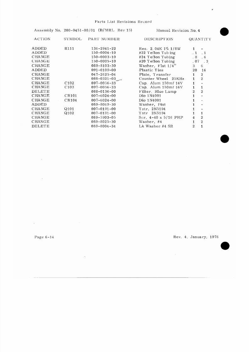
8/9/2019 KX 170A - Maintenance Manual Honeywell
http://slidepdf.com/reader/full/kx-170a-maintenance-manual-honeywell 501/586
Parts List Revisions Record
Assembly No. 200-0451-OO/Ol (i3/MRL Rev 15)
Manual Revision No. 4
A CT ION
ADDED
ADDED
CHANGE
CHANGE
CHANGE
ADDED
CHANGE
CHANGE
CHANGE
CHANGE
DELETE
CHANGE
CHANGE
ADDED
CHANGE
CHANGE
CHANGE
CHANGE
DELETE
SkTMBOL
PART NUMBER
Rlll 136-2941-22
150-0004-10
150-0003-10
150-0005-10
089-8103-30
091-0109-00
047-2625-04
088-0321-03,
Cl02 097-0056-33
Cl03 097-0056-33
088-0136-00
CR101 007-6024-00
CR104 007-6024-00
089-8069-30
QlOl 007-0191-00
Q102 007-0191-00
089-5903-05
089-8025-30
089-8004-34
DESCRIPTION
Res. 2. 04K 1% 1/8W
#22 Teflon Tub ing
#24 Teflon Tubing
#20 Teflon Tubing
Washer, Flat l/4”
.Plastic Ties
Plate, Transfer
Counter Wheel 25KHz
Cap. Alum 150mf 16V
Cap. Alum 150mf 1617
Filter, Blue Lamp
Dio lN4001
Dio lN4001
Washer, FAat
Tstr, 2N5194
Tstr 2N5194
Scr, 4-40 x 5/16 PHP
Washer, #4
Lk Washer #4 SR
QUANTITY
1 -
.l .1
.8 .6
.07 .3
3 6
20 16
1 2
1 2
1 -
1 1
2 2
1 -
1 -
1 -
1 -
1 1
4 2
1 2
2 1
Page 6-14
Rev. 4, January, 1976
0

8/9/2019 KX 170A - Maintenance Manual Honeywell
http://slidepdf.com/reader/full/kx-170a-maintenance-manual-honeywell 502/586
NAME ASS’Y. NO.
1
SWITCH WAFER ASSEMBLIES
ZOO-0575
01
05
1
KING RADIO CORP. PARTS LISTING
I
?
QUANTITY
1
T
PART NUMBER DESCRIPTION
1
200-0575-00
200-0575-01
200-0575-02
200-0575-03
200-0575-04
-
-03
-
X
200-0575-05
Switch Ass'y COMM S103
Switch Ass'y NAV 5105
Switch Ass'y NAV S106
Switch Ass'y NAV S108
Switch Ass'y COMMS102
(KX 170A/175/KY195 Only)
Switch Ass'y COMMS103/1
(KY195B)
150-0003-10
150-0004-10
Tubing, Teflon #24ga
Tubing, Teflon #22ga
CR101
007-6033-00
Diode lN270
CR102
007-6033-00
Diode lN270
CR105
007-6033-00
Diode lN270
CR106 007-6033-00
Diode lN270
CR107 007-6033-00 Diode lN270
CR108
007-6033-00
Diode lN270
CR109
007-6033-00
Diode lN270
CR110
007-6033-00
Diode lN270
CR111
007-6033-00
Diode lN270
CR112
007-6033-00
Diode lN270
CR113 007-6033-00
Diode lN270
CR114 007-6033-00
Diode lN270
-
-02
-
X
.2
4
s102 031-0107-00
Wafer, Switch
s105 031-0154-00
Wafer, Switch
S106
031-0155-00
Wafer, Switch
S108 031-0157-00
Wafer, Switch
s103
031-0205-00
Wafer, Switch
Rlll
136-2941-22 Res, 2.94K 1% QW
R112
136-4020-22
Res, 402 ohm 1% QW
R113
136-4530-22
Res, 453 ohm 1% QW
R114
136-5110-22
Res, 511 ohm 1% QW
R115
136-5620-22 Res, 562 ohm 1% QW
R116
136-6340-22 Res, 634 ohm 1% QW
R117 136-6980-22
Res, 698 ohm 1% QW
R118
136-7870-22 Res, 787 ohm 1% QW
R119
136-8660-22 Res, 866 ohm 1% QW
R120
136-6340-22
Res, 634 ohm 1% QW
R135
136-2941-22
Res, 2.94K 1% QW
R136
136-4020-22 Res, 402 ohm 1% QW
R137 136-4530-22 Res, 453 ohm 1% QW
R138 136-5110-22 Res, 511 ohm 1% QW
R139
136-5620-22
Res, 562 ohm 1% QW
R140
136-6340-22 Res, 634 ohm 1% QW
R141 136-6980-22 Res, 698 ohm 1% QW
R142
136-7870-22
Res, 787 ohm 1% QW
R143
136-8660-22 Res, 866 ohm 1% QW
R144
136-6340-22 Res, 634 ohm 1% QW
_ i _
- j -
1 1 1
- -
?
ev.
4, January, 1976
I
SHTLOFL
-04
-I=
I
X I
I
1 x
I
- i .l
.l
- I -
I -
1
1
1
1 1
1 1
1 1
1 1
1 I1
1 p
: 1:
1 1
1 1
1 1 1
1 i 1
1 1I
1 i 1
1 1
I
1
1
I1
1 1
I
1 i 1
i
Page 6-14A
i
K-1651
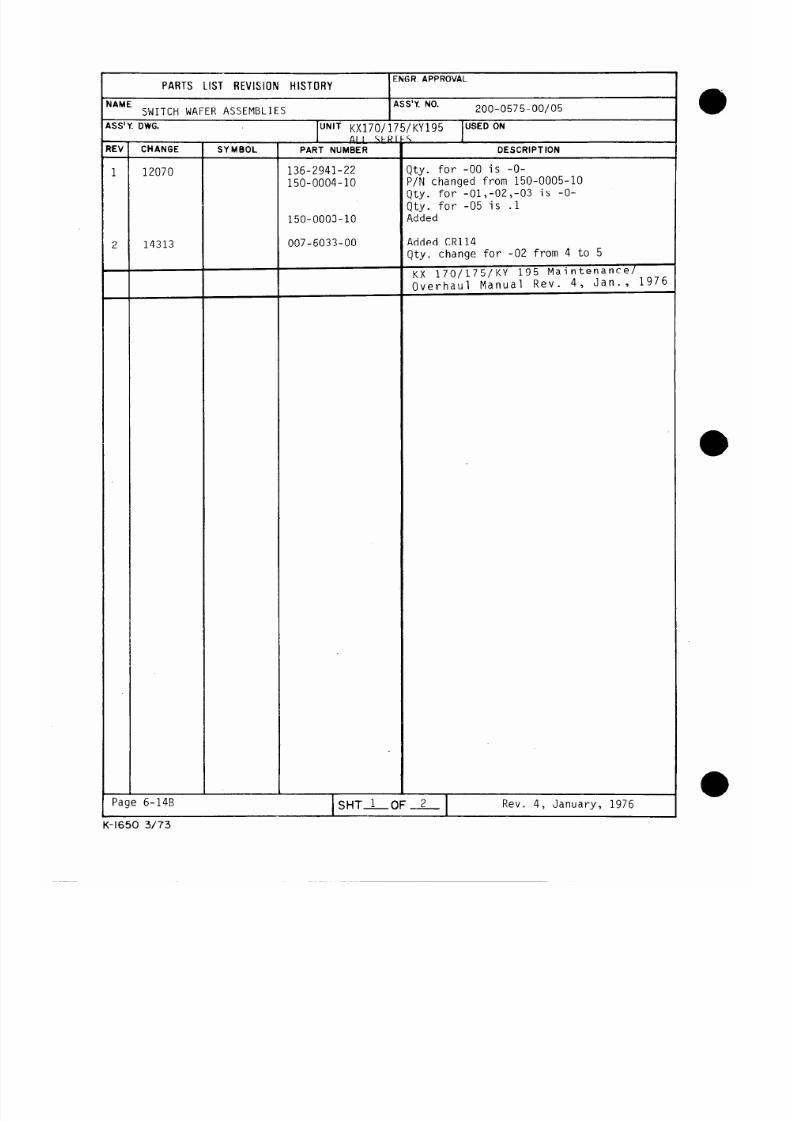
8/9/2019 KX 170A - Maintenance Manual Honeywell
http://slidepdf.com/reader/full/kx-170a-maintenance-manual-honeywell 503/586
r
NSS Y. DWG.
Qty. for -00 is -O-
P/N changed from 150-0005-10
Qty. for -Ol,-02,-03 is -O-
Qty. for -05 is
.l
Page 6-14B
hT1OF 2 1
Rev. 4, January, 1976
K-1650 3/73

8/9/2019 KX 170A - Maintenance Manual Honeywell
http://slidepdf.com/reader/full/kx-170a-maintenance-manual-honeywell 504/586
089-5381-20 -._
t-21
A
083~a$f3-30- ---x.>~
076-0298-O i -
(2)
?50- 0003 L 0
f? ?c-c~%
1
026-OOOI-00
(6 T=bcra)
Og3-2140-00‘ (2’1
ooe- 0005-03
(2)
047-2bZ
/’
/
_/”
,_.’
,/’
,
_’
/’
,A’
./’
A””
__”
,.I’
,/’
/ A /
x\ ,,I
008-000503
7,
r
150-co20 - 10
/
~047-1675-01
\‘-069-2140-00 C2)
‘,
2. WASHERS AS REQ”RED TO INSURE A L IGHT TGHT ASEMELY OF DIAL5
KX 170B/KX 175B
FIGURE 6-4 SWITCHING HEAD SUB-ASSEMBLY
(Dwg. No. 300-0650-00
R-lO)(Sht. 1 of 2)
Rev. 4,
January, 1976
Page 6-15

8/9/2019 KX 170A - Maintenance Manual Honeywell
http://slidepdf.com/reader/full/kx-170a-maintenance-manual-honeywell 505/586
PI34
PIGI
5106
105
230-0375.01
/9
WIRING CHART
1
To
NAV SMO
300-O&58-00
BUNDLE A
IO
f0
A--+--: /I
To Corm .Sr?o
300-0656-
1. UNLFSS NO7 YD-
+*zLAWG COPPERW&LO-025-OOB-XX
#Z&ciG BUSS
- 0 26 -o o o\ - 0 0
2 _ SLEEVf W/TH /5-O-0003-/0.
3.
ST/?/P
#TIM . PO FROM ENO, ALL W/RES.
FIGURE 6 -4A SWITCHING HEAD SUB-ASSEMBLY
(Dwg. No. 300-0650-00 R-lO)(Sht. 2 of 2)
Rev. 4, January, 1976
Page 6-17

8/9/2019 KX 170A - Maintenance Manual Honeywell
http://slidepdf.com/reader/full/kx-170a-maintenance-manual-honeywell 506/586
KM’TOU ltd5~b.TOR 1”
I
4 PP L. y T HE F2 MI L CO V h PO UN D O lb -1 00 4 .0 0 O N B OT H
Q
QIOS I 047-2624-02.
R\3
--OS+8\00-30
ceo-oom- 0 I
04-(-Z&,24- O-Z ~- --
047-1675-O\
/
‘003-2l40-OO(2)
,
/
/
.A
./-
,.,’ _, ..
’
/
/’ ._
I
/
/
A
/ ’
/
,/”
,.’
‘_
--L
A
/
.
.
/
016-0290-03t2~~
-200-0576-04
,
_/ ‘ x_
047-2620&~
\
oe 9 -zag 31(2)7\
‘_.
‘ m ~Po\o&oool-ol
r=+
_ o1
.
.
._
080 - 0232-o\\
-1 ‘
S E E V IE W Q -L h \
.x
‘sxY?eoZFW
7
’ .Y__
AWL--I \50-COZO-IO To 00%0~05-03 (5 Pa-&~
047-2635-00
‘
2.
.
.-OSI-0\04-00(5\02)
‘-076-0230-O\~‘L)
‘ - - 076-0298-07 (2)
037-0007-10 (04lOl)
089.2140.OO(2b
-008-b ~os-o3(2J
090-0160-00
088-0321-03 A
-oe9-aloo-
090-0019-o I
04-I-2625-04 A
’
;-G,“~~o-::,‘,“,;“:,., 3
ONE TOOTU OF 3 TOOTH GCAR-
1’
“-- -*ATE WLTH 0\6-1016-00
M US T P OI NT T O WA RD C EN TE R
AXIS OF TRAN3FEn PLATE,041-2G7.5.Ol
VIEW A-A
,76-00
a ^ ___e
KY 1958
FIGURE 6-5 SWITCHING HEAD SUB-ASSEMBLY
(Dwg. No. 300-0651-OO)(Sht. 1 of 2) R-6
Rev. 4, January, 1976
Page 6-19

8/9/2019 KX 170A - Maintenance Manual Honeywell
http://slidepdf.com/reader/full/kx-170a-maintenance-manual-honeywell 507/586
,- PLOT NEL/W -T)
,- P\\I(GRY)
PI06 (Si02j
PIII (5\03)
iPI (SIO3) ” RI-l55
P192. (5106) /GREY
Pl6(SlO3) ‘Pi91 (5106) ‘BROWN
PI66 (5104) .P17o~Il3(slos~ cuss
p 1104 73(5105) P 185 (SLO6) e.USS
P 193 (SIOL)
P sz(UOTE3) ‘REO/BLU
P 195 (5106)
P 179cNOTE4) j DLACK
L_AMP WtU\NG CUART
FROM
TO
PEM*RKs
05 \OI [WIG) i P 124 (5\03) : 5==E SUEET 1
DS\Ol (SLY) PI\7 (5102) : ”
”
D5lOZ(Wc\T) / PII7 (5\02\) / )
‘I 8’
No-resi
,. UNLESS NOTED:
ALL WIRE ‘ZG. AwG.COPPERWELD
025-oo,e- sx, ccxoq PER CUARTS.
BUSS WIRE, l 2GAWG. 026.OOO\-00
AND SLhEVED WITH I50-0003-\a
2. STR\P.f TIN .20 FROM =hD, ALLWLRES
3. TO FRONT PLATE ASSY., 300-0648-00
4. SEE SUEET I FOR CONNECT\ONS.
Pl0-L ”
P1O- (5102)
P\Oe. (S\O3)
PI09 ”
PI14 11
PI20 ”
PI21 ‘1
PI22 ”
PI2;(5\03)
P \a3 (5iO4)
PIG.9 cs104\
PI71 ISIO5)
PI12 ”
PlS2 81
PI83 ”
PI 84 (5\05)
PI86 (5\06)
PI87 @I
P\88 I’
pfa5 ~5106~
P245
PI.51
P265
P266
P269
P261
P260
P241
P253
P260
P263
P262
P261
I=‘255
P250
P250
P289
P288
P287
PtS6
P285
PZBC
P261
P282
P283
LENGT U
FIGURE
6-5A SWITCHING HEAD SUB-ASSEMBLY
(Dwg. No. 300-0651-OO)(Sht. 2 of 2) R-6
Rev. 4, January, 19’76
-
5101,102, I93
~WITCHlbG
AEAt 14
sue- AS'3Y.
BUNDLE A=sY.
330-C&5\-00
300-O&5\-01
Page 6-21

8/9/2019 KX 170A - Maintenance Manual Honeywell
http://slidepdf.com/reader/full/kx-170a-maintenance-manual-honeywell 508/586
R4
KING RADIO CORf? PARTS LISTING
SYMBOL 1
Q201
Q202
Q203
Q206
Q207
Q208
Q209
Q210
Q211
Q212
007-0238-00
007-0195-00
007-0195-00
007-0238-00
007-0238-00
007-0238-00
007-0195-00
007-0078-00
007-0078-00
007-0046-00
Tstr FPN4917
Tstr MPS-HlO
Tstr MPS-HlO
Tstr FPN4917
Tstr FPN4917
Tstr FPN4917
Tstr MPS-HlO
Tstr 2N3415
Tstr 2N3415
Tstr 2N3605
CR201
CR202
CR203
CR204
CR205
CR206
CR207
CR208
CR209
CR210
CR214
CR215
007-4012-00
007-6033-00
007-6045-00
007-6045-00
007-6045-00
007-6045-00
007-6045-00
007-6045-00
007-6045-00
007-6045-00
007-5016-00
007-6035-00
Dio Vctr SMV626
Dio lN270
Dio FHllOO
Dio FHllOO
Dio FHllOO
Dio FHllOO
Dio FHllOO
Dio FHllOO
Dio FHllOO
Dio FHllOO
Dio 5. 1V 5% 1W
Dio lN816
R261
015-0023-00
Res 4. 7K 2070 2W
L201
019-2151-00
1~202
019-2082-70
L203
019-2054-16
L204
019-2054-16
L205 019-2054-13
L206
019-2084-40
Coil VCO
Choke Mld 240ph 5%
Choke Dip 1. Oph 5%
Choke Dip 1. Oph 5%
Choke Dip . 56yh 5%
Choke Mld 6. 8ph 5%
PART NUMBER
009-5249-01
012-1038-00
025-0018-22
025-0018-99
026-0001-00
026-0013-00
047-2154-00
088-0066-00
090-0104-04
150-0003-10
150-0015-10
DESCRIPTION
NAV SMO Board
Adh Disc. 312 Dia
#26 Wire Red
#26 Wire
Wht
#26 Wire
Coax Cable RG178
Can VCO Coil
Spacer Xtal
Solder Ring
Tubing Teflon #24
Tubing Teflon #12
200-0457-00
1
1
5
6
8
.
1
1
12
4
1
1
1
1
1
1
1
1
1
1
1
1
1
1
1
1
1
1
1
1
1
1
1
1
1
1
1
1
1
1
QUANTITY
= =
=
-
Rev. 4, January, 1976
Page 6-23

8/9/2019 KX 170A - Maintenance Manual Honeywell
http://slidepdf.com/reader/full/kx-170a-maintenance-manual-honeywell 509/586
KING RADIO CORF? PARTS LISTING
SYMBOL
L207
T201
T202
T203
T204
T205
T206
T2’l7
T208
CJ201
Y201
Y202
c201
c202
C203
C204
C205
C206
C208
c210
c211
c212
C213
C214
C215
C216
C217
C218
c219
c220
c221
c222
C223
C224
C225
C226
C227
C228
c229
C230
PART NUMBER
019-2084-06
019-2109-00
019-3044-00
019-3044-00
019-5056-02
019-5056-02
019-5056-02
01 g-5056-02
019-2109-02
026-0018-00
044-002 7-00
044-0028-01
114-5152-00
096-1030-22
114-5152-00
118-0003-00
118-0003-00
113-5331-00
113-5681-00
096-1030-05
114-7104-00
105-0031-09
113-7503-00
096-1030-22
096-1030-22
113-3150-00
113-5681-00
113-5681-00
113-5471-00
113-3100-00
113:5681-00
113-5681-00
113-5471-00
113-5101-01
113-3330-00
114-5152-00
114-5142-00
114-5152-00
114-5152-00
113-3082-00
DESCRIPTION
Choke Mld . 2 7ph 5’%
Ind Var 22mh
Tfmr RF Buffer
Tfmr RF Buffer
Tfmr Mixer
Ye1
Tfmr Mixer
Ye1
Tfmr Mixer
Ye1
Tfmr Mixer
Ye1
Ind Var 22mh
Circuit Jumper
Xtal 53. 93125MHz
Xtal 400KHz
Cap DC 1500pf 10%
Cap Tant 22pf 1OV
Cap DC 1500pf 10%
Cap DC 56pf 5%
Cap DC 56pf 5%
Cap DC 330pf 10%
Cap DC 680pf 10%
Cap Tant 10pf 15V
Cap DC . lpf 12V
Cap My1 , 0022pf 80V
Cap DC 05pf 12V
Cap Tant 22pf 1OV
Cap Tant 22pf 101’
Cap DC 15pf 5%
Cap DC 68Opf 10%
Cap DC 680pf 10%
Cap DC 470pf 10%
Cap DC 1Opf N150
Cap DC 680pf 10%
Cap DC 680pf 10%
Cap DC 470pf 10%
Cap DC 1OOpf 10%
Cap DC 33pf 5%
Cap,DC 1500pf 10%
Cap DC 1500pf 10%
Cap DC 1500pf 10%
Cap DC 1500pf 10%
Cap DC 8. 2pf N150
i-00
200-0457-00
=
00
-
1
1
1
1
1
1
1
1
1
1
1
1
1
1
1
1
1
1
1
1
1
1
1
1
1
1
1
1
1
1
1
1
1
1
1
1
1
1
1
1
QUANTITY
= = =
-
=
Page G-24
Rev. 4, January, 1976

8/9/2019 KX 170A - Maintenance Manual Honeywell
http://slidepdf.com/reader/full/kx-170a-maintenance-manual-honeywell 510/586
SYMBOL
PART NUMBER
DESCRIPTION
C231
C232
C233
C234
C235
(‘236
C237
C238
c-239
C240
C241
C242
C243
C244
C245
C246
C247
C248
C252
C253
C254
C255
C256
C257
C258
c259
C260
C261
C262
C264
C265
C266
C267
C268
C270
C271
113-3100-00
113-3270-00
113-3100-00
114-5152-00
113-3470-00
113-3820-00
i14-5152-00
114-5152-00
113-5151-01
113-5151-01
114-7104-00
113-5681-00
114-7104-00
096-1030-22
114-7104-00
096-1030-22
114-7104-00
096-1030-22
106-0034-00
106-0034-00
106-0034-00
106-0034-00
106-0034-00
106-0034-00
106-0034-00
106-0034-00
106-0034-00
106-0034-00
106-0034-00
114-7104-00
096-1030-22
113-5681-00
114-7104-00
113-5471-00
106-0034-00
113-7503-00
Cap DC 1Opf N150
Cap DC 27pf N150
Cap DC 10pf N150
Cap DC 1500pf 10%
Cap DC 47pf 5%
Cap DC 82pf 5%
Cap DC 1500pf 10%
Cap DC 1500pf 10%
Cap DC 150pf 10%
Cap DC 150pf 10%
Cap DC . lpf 12V
Cap DC 680pf 10%
Cap DC lpf 12V
Cap Tant 22pf 1OV
Cap DC . lj f 12V
Cap Tant 22pf 1OV
Cap DC , lpf 12V
Cap Tant 22pf 1OV
Cap FT 1. 5Kpf 20%
Cap FT 1. 5Kpf 20%
Cap FT 1. 5Kpf 20%
Cap FT 1, ,5Kpf 20%
Cap FT 1. 5Kpf 20%
Cap FT 1. 5Kpf 20%
Cap FT 1. 5Kpf 20%
Cap FT 1. 5Kpf 20%
Cap FT 1. 5Kpf 20%
Cap FT 1. 5Kpf 20%
Cap FT 1. 5 Kpf 20%
Cap DC . ll.tf 12V
Cap Tant 22pf 1OV
Cap DC 680pf 10%
Cap DC . lpf 121’
Cap DC 470pf 10%
Cap FT 1. 5Kpf 20%
Cap DC , 05pf 12V
1201 120-0019-00 IC U6B902059X
1202 120-0021-00
IC U6B930059X
1203
120-0001-00
IC SN7400N
1204 120-0004-00
IC SN7420N
1206 120-0021-00
IC U6B930059X
1210
120-0011-00
Ic’ SN7493N
1211 120-0001-00
IC SN7400N
KING RADiO CORP PARTS LISTING
200-0457-00
QUANTITY
z
-
1
1
1
1
1
1
1
1
1
1
1
1
1
1
1
1
1
1
1
1
1
1
1
1
1
1
1
1
1
1
1
1
1
1
1
1
1
1
1
1
1
1
1
-
=
= =
-
Rev. 4, January, 1976
Page 6-25

8/9/2019 KX 170A - Maintenance Manual Honeywell
http://slidepdf.com/reader/full/kx-170a-maintenance-manual-honeywell 511/586
.
R4
R4
SYMBOL
1212
R201
R202
R203
R204
R205
R206
R208
R209
R210
R214
R215
R216
R217
R218
R219
R220
R221
R222
R223
R224
R225
R,226
R227
R228
R229
R230
R231
R232
R233
R234
R235
R236
R237
R238
R239
R240
R241
R242
R243
R244
R245
R258
KING RADIO CORF PARTS LISTING
PART NUMBER
120-0008-00
130-0101-25
130-0103-23
130-0471-23
130-0362-23
130-0510-23
130-0473-25
130-0151-23
130-0751-23
130-0112-23
130-0112-23
130-0152-25
130-0101-25
130-0392-23
130-0242-23
130-0271-23
130-0101-25
130-0392-23
130-0392-23
130-0271-23
130-0272-23
130-0221-23
130-0512-23
130-0101-23
130-0151-23
130-0470-25
130-0100-23
130-0470-23
130-0301-23
130-0101-25
130-0222-23
130-0911-23
130-0132-23
130-0302-23
130-0331-23
130-0201-23
130-0241-23
130-0820-23
130-0471-23
130-0471-23
130-0472-23
130-0472-23
130-0102-25
DESCRIPTION
IC
SN7474N
Res FC 100 5% QW
Res FC 10K 5% QW
Res FC 470 5% QW
Res FC 3. 6K 5% QW
Res FC 51 5% QW
Res FC 47K 10% QW
Res FC 150 5% QW
Res FC 750 5% QW
Res FC 1. 1K 5% QW
Res FC 1. 1K 5% QW
Res FC 1. 5K 10% QW
Res FC 100 10% QW
Res FC 3. 9K 5% QW
Res FC 2.4K 5% QW
Res FC 270 5% QW
Res FC 100 10% QW
Res FC 3. 9K 5% QW
Res FC 3. 9K 5% QW
Res FC 270 5% QW
Res FC 2. 7K 5% QW
Res FC 220 5% QW
Res FC 5. 1K 5% QW
Res FC 100 5% QW
Res FC 150 5% QW
Res FC 47 10% QW
Res FC 10 5% QW
Res FC 47 5% QW
Res FC 300 5% QW
Res FC 100 10% QW
Res FC 2. 2K
5%
QW
Res FC 910
5’7’0
QW
Res FC
1. 3K
570
QW
Res FC 3K 5% QW
Res FC
330 570 QW
Res FC 200 5% QW
Res FC 240 5% QW
Res FC 82 5% QW
Res FC
470 570 QW
Res FC 470 5% QW
Res FC 4. 7K 5% QW
Res FC 4. 7K 5% QW
Res FC 1K 5% QW
11 200-0457-00
=
oc
-
1
1
1
1
1
1
1
1
1
1
1
1
1
1
1
1
1
1
1
1
1
1
1
1
1
1
1
1
1
1
1
1
1
1
1
1
1
1
1
1
1
1
1
QUANTITY
=
-
Page 6-26
Rev. 4, January, 1976
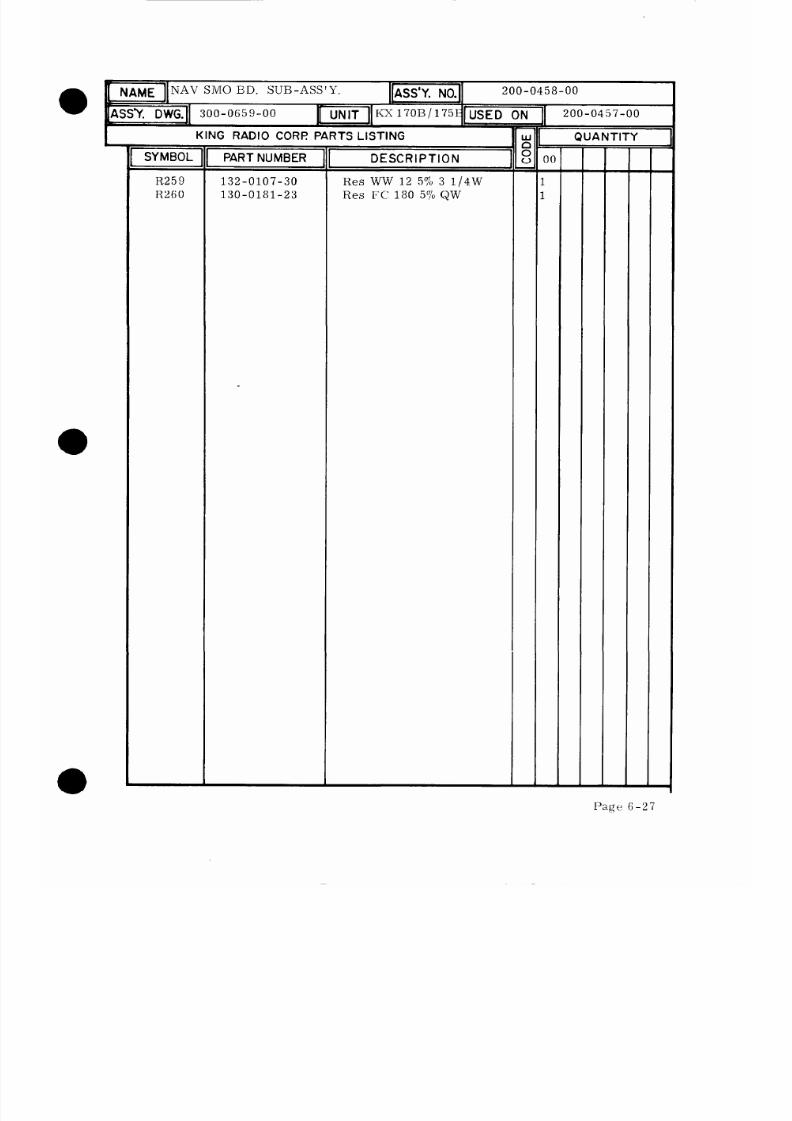
8/9/2019 KX 170A - Maintenance Manual Honeywell
http://slidepdf.com/reader/full/kx-170a-maintenance-manual-honeywell 512/586
NAV SMO ED. SUB-ASS’Y.
200-0458-00
DWG.11 300-0659-00
r UNIT h’= 170W175E~
KING RADIO CORl? PARTS LISTING
ii
I
200-0457-00
QUANTITY
SYMBOL
PART NUMBER
DESCRIPTION
R259
R260
-
i
[
I
132-0107-30
Res WW 12 5% 3 1/4W
130-0181-23 Res FC 180 5% QW
Page F-

8/9/2019 KX 170A - Maintenance Manual Honeywell
http://slidepdf.com/reader/full/kx-170a-maintenance-manual-honeywell 513/586
Parts List Revisions Record
Assembly No. 200-0458-00 (B/MRL Rev 13)
Manual Revision No. 4
ACTION
SYMBOL PART NUMBER
DESCRIPTION
QUANT IT Y
CHANGE R230 130-0047-23 Res F/C 4. 7R 5’70QW 1
ADDED 091-0196-00
Spacer
2
CJftANGE R228
130-0101-23
Res F/C 1OOG
57’0
QW
1
ADDED R262
130-0133-23
Res F/C 13K 5% QW
1
CHANGE Q212 007-0113-00 Tstr 2N3646 1
Page 6-28
Rev. 4, January, 1976
a
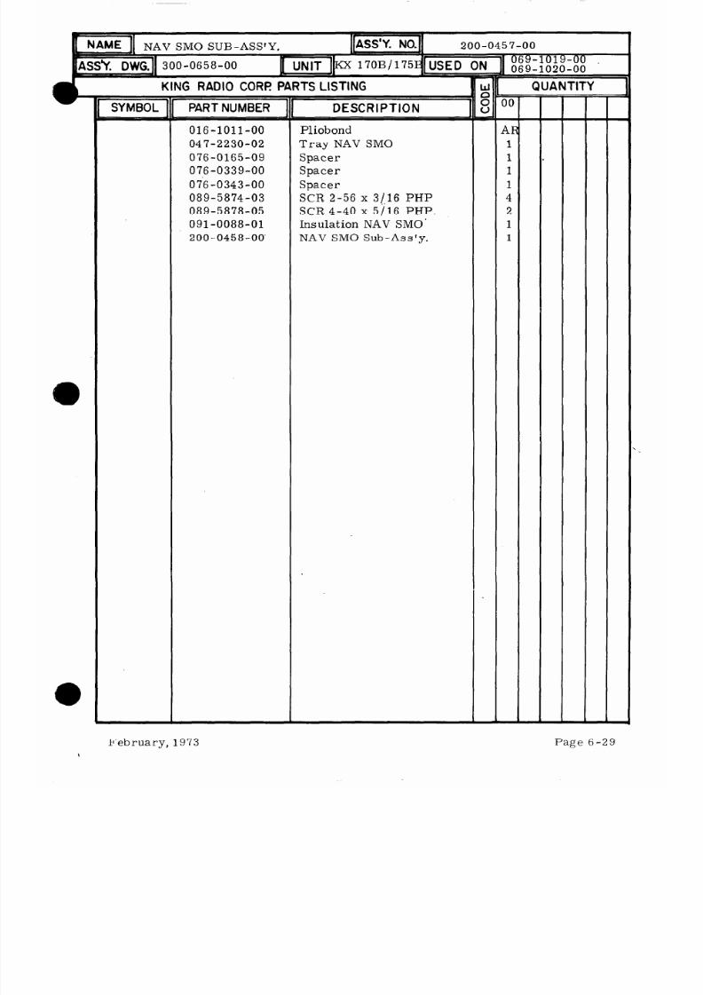
8/9/2019 KX 170A - Maintenance Manual Honeywell
http://slidepdf.com/reader/full/kx-170a-maintenance-manual-honeywell 514/586
NAV SMO SUB-ASS’Y.
200-0457-00
SS'V. DWd300-0658-00
069-1019-00
069-1020-00
KING RADIO CORf? PARTS LISTING
SYMBOL
PART NUMBER
016-1011-00
047-2230-02
076-0165-09
076-0339-00
07'6-0343-00
089-5874-03
089-5878-05
091-0088-01
200-0458-00.
DESCRIPTION1
Pliobond
Tray NAV SMO
Spacer
Spacer
Spacer
SCR 2-56 x 3116 PHP
SCR 4-40 x 5/16 PHP
Insulation NAV SMO’
NAV SMO Sub-Ass’y.
00
ri
1
1
1
1
4
2
1
1
QUANTITY
=
-
-
February, 1973
Page 6-29

8/9/2019 KX 170A - Maintenance Manual Honeywell
http://slidepdf.com/reader/full/kx-170a-maintenance-manual-honeywell 515/586
Parts List Revisions Record
Assembly No. 200-0457-00
ACTION
SYMBdL PART NUMBER
Manual Revision No. 0
DESCRIPTION
QUANTITY
Page 6-30 February, 1973

8/9/2019 KX 170A - Maintenance Manual Honeywell
http://slidepdf.com/reader/full/kx-170a-maintenance-manual-honeywell 516/586
076-O 1339-00
REF:
KlNG
KX 170B/KX 175B
NAVIGATION RECEIVER/
COMMUNICATIONS TRANSCEIVER
076- 0343-00
nh
\
\
076-0165-09
089-5874-03(4)
P201. I/I /ix7
200-0458-00
\089-5878-05(2)
February, 1973
FIGURE 6-6 NAV SMO SUB-ASSEMBLY
(Dwg. No. 300-0658-00)
Page 6-31

8/9/2019 KX 170A - Maintenance Manual Honeywell
http://slidepdf.com/reader/full/kx-170a-maintenance-manual-honeywell 517/586
NAME 11 rnlvln/l sn/ln Rl
-_.__._ Y_.IV l
300-0657-00
1 UNIT 11” nr Iy3r,
,,----
3. SUB -ASS’Y
ASS’Y. NO.
230-0456
%%/,1,75R%lSED ON I
II
00-0455-OO/Ol
bflhlr, PAnlA t-ADD DADTC I ICTlLlr?
‘R4
SYMBOL
Q301
0302
Q303
Q304
Q305
Q306
0307
9310
Q311
Q312
Q313
Q315
Q316
Q317
Q318
150-0003-10
150-0005-10
150-0015-10
007-0195-00
007-0238-00
007-0195-00
007-019.5-00
007-0195-00
007-0195-00
007-0078-00
007-0195-00
007-0238-00
007-0238-00
007-0195-00
007-0078-00
007-0078-00
007-0046-00
007-0078-00
Comm SMO Board
Comm SMO Board
Adh D isc . 312Dia
Wire #26
Wht/Brn
Wire #26 Wht/Gry
Wire #26 Wht
Wire #2’6
Coax Cable RG 178
Enclosure, VCO
Enclosure, Osc.
Spacer Crystal
Solder Ring
%
24 Teflon Tubing
20 Teflon Tubmg
#12 Teflon Tubing
Tstr MPS-HlO
Tstr FPN4917
Tstr MPS-HlO
Tstr MPS-HlO
Tstr MPS-HlO
Tstr MPS-HlO
Tstr 2N3415
Tstr MPS-HlO
Tstr FPN4917
Tstr FPN4917
Tstr NIPS-H10
Tstr 2N3415
Tstr 2N3415
Tstr 2N3605
Tstr 2N3415
CR301 007-6035-00
Dio lN816
CR302
007-6035-00
Dio, lN816
CR303
007-4012-00
Dio, Vctr SMV626
CR304
007-6033-00
Dio, lN270
CR305 007-6045-00 Dio, FHllOO
CR306
007-6045-00
Dio, FHllOO
CR307 007-6045-00
Dio, FHllOO
CR308 007-6045-00 Dio, FHllOO
CR309 007-6045-00
Dio, FHllOO
CR310
007-6045-00
Dio, FHllOO
CR311
007-6045-00
Dio, FHllOO
Page 6-32
PART NUMBER
200-0456-00
KX 175B/KY 195B
200-0456-01
Kx 170B
009-5250-01
009-5250-02
512-1038-00
025-0018-91
025-0018-98
025-0018-99
026-0001-00
026-0013-00
047-1853-01
047-2627-01
088-0066-00
090-0104-04
DESCRIPTION
-OO/Ol
E
X
1
1
1.
1.
2.
2.
2.
1
1
2
19
2.
i
1
1
1
1
1
1
1
1
1
1
1
1
1
1
1
1
1
1
1
1
1
1
1
1
1
1
QUANTITY
E
s
1
1
.
.
I.
I
I. I
1
1
2
19
I. ‘
ii
1
1
1
1
1
1
1
1
1
1
1
1
1
1
1
1
1
1
1
1
1
1
1
1
Rev. 4, January, 1976

8/9/2019 KX 170A - Maintenance Manual Honeywell
http://slidepdf.com/reader/full/kx-170a-maintenance-manual-honeywell 518/586
SYMBOL]
CR312
CR313
CR314
CR318
CR319
CR320
CR321
CR322
PART NUMBER DESCRIPTION
007-6045-00
007-6059-00
007-6059-00
007-6033-00
007-5016-00
007-6035-00
007 6070-00
007-6070-00
Dio, FHllOO
Dio, FD400
Dio, FD400
Dio, lN270
Dio, 5. 1V 5% 1W
Dio, lN816
Dio, MPN3401
Dio, MPN3401
R324
015-0023-00
Res 4. 7K 20% 2W
L301
L302
L303
L304
L305
L306
L316
019-2099-01
019-2082-70
019-2054-12
019-2084-10
019-2054-16
019-2084-49
019-2054-06
Choke, Mid. . 13ph 5%
Choke, illld. 240ph 5%
Choke, Dip . 47ph
5%
Choke, Mld. . 39ph 5%
Choke, Dip 1. Oph 5?0
Choke, Mid. 15ph 10?0
Choke, Dip . 15ph 5%
T301
T302
T303
T304
T305
T306
T307
T308
019-3044-00
019-5056-02
01 g-5056-02
019-5056-01
019-3044-00
019-5056 -01
019-2109-00
019-2109-00
Tfmr, R. F. Buffer
Tfmr, Mixer
(Yel)
Tfmr, Mixer (Yel)
Tfmr, Mixer
(Blu)
Tfmr, R. F. Buffer
Tfmr, Mixer
(Blu)
Ind, Var 22mh
Ind, \‘ar 22mh
CJ301
CJ302
026-0018-00
026-0018-00
Circuit Jumper
Circuit Jumper
Y301
Y302
Y303
044-0050-01
044-0050-00
044-0028-01
Xtal, 71. 0375MHz
Xtal, 66. 5375MHz
Xtal, 400KHz
c301
106-0034-00
Cap F/T 1. 5Kpf 10%
C302 106-0034-00 Cap F/T 1. 5Kpf 1Ocfn
c303
106-0034-00
Cap F/T 1. 5Kpf 10%
c304
113-5471-00
Cap, DC 470pf
10%
C305
113-3100-00
Cap, DC 1Opf N150
c‘306
106-0034-00
Cap F/T 1. 5Kpf 10%
c307
106-0034-00
Cap F/T 1. 5Kpf 10%
C308
113-5471-00
Cap, DC 470pf 10%
c309
113-5471-00
Cap, DC 470pf 10%
KING RADIO CORF PARTS LISTING
I200-0455-O?/Ol
00
T
1
1
1
1
1
1
1
1
1
1
1
1
1
1
1
1
1
1
1
1
1
1
1
1
1
1
1
1
1
1
1
1
1
1
1
1
1
QUANTITY
7
T
1
1
1
1
1
1
1
1
1
1
1
1
1
1
1
1
1
1
1
1
1
1
1
1
1
1
1
1
1
1
1
1
1
1
1
1
= =
-
February, 1973 Page 6-33

8/9/2019 KX 170A - Maintenance Manual Honeywell
http://slidepdf.com/reader/full/kx-170a-maintenance-manual-honeywell 519/586
R4
R4
R4
R4
SYMBOL
KING RADIO CORf? PARTS LISTING
c310
c311
c312
c314
c315
C316
c317 .
C318
c319
‘C320
C321
C322
C323
C324
C325
C326
C327
C328
c-329
c330
c331
C332
c333
c334
c335
C336
c337
c338
(7339
c340
c341
C342
c343
c344
c345
C346
c347
C348
c349
c350
c351
C352
c353
c354
PART NUMBER
113-5471-00
113-5471-00
113-5471-00
102-0024-09
102-0029-00
096-1030-22
113-2370-00
113-5471-00
106 -0034 -00
113-5471-00
113-5471-00
114-7104-00
113-5471-00
113-5102-00
113-3100-00
113-3082-00
113-5331-00
114-7104-00
113-5471-00
113-3015-00
106-0034-00
102-0009-37
113-5471-00
102-0009-37
113-3120-00
113-5471-00
113-5471-00
113-3270-00
113-5471-00
113-5471-00
113-6103-00
113-5331-00
109- 0008-00
113-5471-00
113-7203-00
118-0007-00
096-1030-05
113-7503-00
105-0031-09
114.-7104-00
114-7104-00
096-1030-22
096-1030-22
113-3270-00
DESCRIPTION
Cap, DC 470pf 10%
Cap, DC 470pf 10%
Cap, DC 470pf 10%
Cap, Var 7-35pf
Cap, Var 2-27pf
Cap, Tant 22pf 1OV
Cap, DC Z7pf N150
Cap, DC 470pf
Cap, F/T 1. 5Kpf 10%
Cap, DC 470pf
Cap, DC 470pf
Cap, DC 1Kpf 12V
Cap, DC 470pf
Cap, DC 1000pf
Cap, DC 1Opf N150
Cap, DC 8. 2pf N150
Cap, DC 330pf
Cap, DC 1Kpf 12V
Cap, DC 470pf
Cap, DC 1. 5pf N150
Cap, F/T 1. 5Kpf 10%
Cap, Var 9-35pf N650
Cap, DC 470pf
Cap, Var 9-35pf N650
Cap, DC 12pf N150
Cap, DC 470pf
Cap, DC 470pf
Cap, DC 27pf N150
Cap, DC 470pf
Cap, DC 470pf
Cap, DC . Olpf 50V
Cap, DC 330pf
Cap, Tub 3. Opf N330
Cap, DC 470pf
Cap, DC . 02pf 12V
Cap, Cer 33pf N1500
Cap, Tant 10pf 20V 10%
Cap, DC 05pf 12V 20%
Cap, My1 . 0022pf 8OV
Cap, DC 1Kpf 12V
Cap, DC 1Kpf 12V
Cap, Tant 22pf 1OV
Cap, Tant 22pf 1OV
Cap, DC 27pf N150
200-0455-00/O
3
IO
1
1
1
1
1
1
1
1
1
I
1
1
1
1
1
1
1
1
1
1
1
1
1
1
1
1
1
1
1
1
1
1
1
1
1
1
1
1
1
1
1
1
1
1
QUANTITY
=
11
1
1
1
1
1
1
1
1
1
1
1
1
1
1
1
1
1
1
1
1
1
1
1
1
1
1
1
1
1
1
1
1
1
1
1
1
1
1
1
1
1
1
1
1
=
-
=
=
Page 6-34
Rev. 4, January, 1976

8/9/2019 KX 170A - Maintenance Manual Honeywell
http://slidepdf.com/reader/full/kx-170a-maintenance-manual-honeywell 520/586
R4
R4
R4
R4
R4
R4
SYMBOL
KING RADIO COW PARTS LISTING
PART NUMBER
c355
(1356
c357
C358
c359
C360
C361
C362
C363
C364
C365
C366
C367
C368
C369
c370
c37i.
C372
c373
c374
c375
C376
c377
C378
c379
C380
C381
C385
C386
C387
C388
C389
c390
c391
c392
c393
c395
c399
c551
C553
c555
C562
C563
C564
106 -0034 -00
114-7104-00
114-5152-00
114-5152-00
114-5152-00
113-3120-00
113-5331-00
113-3056-00
113-5151-01
113-3068-00
113-3033-00
113-5560-00
114-5152-00
114-5152-00
114-7104-00
113-7503-00
113-7503-00
106-0013-00
106-0013-00
106-0013-00
113-5151-01
113-5151-01
114-7104-00
114-7104-00
096-1030-22
113-5681-00
114-7104-00
106-0034-00
106-0034-00
109-0008-01
106-0034-00
106-0034-00
105-0031-26
106-0034-00
113-7503-00
106-0034-00
106’-0034-00
106-0034-00
106-0034-00
106-0034-00
106-0034-00
114-7104-00
096-1030-22
096-1030-11
Xev. 4, January, 1976
DESCRIPTION
Cap,
F/T 1. 5Kpf 10%
Cap, DC 1Kpf 12V
Cap, DC 1500pf
Cap, DC 1500pf
Cap, DC 1500pf
Cap, DC 12pf N150
Cap, DC 330pf
Cap, DC 5. 6pf N150
Cap, DC 150pf
Cap, 6. 8pf N150 500V
Cap, DC 3. 3pf 500V
Cap, DC 56pf 10%
Cap, DC 1500pf
Cap, DC 1500pf
Cap, DC 1Kpf 12V
Cap, DC . 05yf 20% 12V
Cap, DC . 05pf 20% 12V
Cap, F/T 3Kpf
Cap, F/T 3Kpf
Cap, F/T. 3Kpf
Cap, DC 150pf
Cap, DC 150pf
Cap, DC 1Kpf 12V
Cap, DC 1Kpf 12V
Cap, Tant 22pf 1OV
Cap, DC 680pf
Cap, DC 1Kpf 12V
Cap, F/T 1. 5Kpf 10%
Cap, F/T 1. 5Kpf 10%
Cap, Tub 4. 3pf N3300
Cap, F/T 1. 5Kpf 10%
Cap, F/T 1. 5Kpf 10%
Cap, Myl. . 0068pf 80V
Cap, F/T 1. 5Kpf 10%
Cap, DC . 05pf 12V
Cap, F/T 1. 5Kpf 10%
Cap, F/T 1. 5Kpf 10%
Cap, F/T 1. 5Kpf 10%
Cap, F/T 1. 5Kpf 10%
Cap, F/T 1. 5Kpf 10%
Cap, F/T 1. 5Kpf 10%
Cap, DC 1Kpf 12V
Cap, Tant 22pf 1OV
Cap, Tant 4. 7pf 20V
[ 200-0455-OO/Ol
G
1
1
1
1
1
1
1
1
1
1
1
1
1
1
1
1
1
1
1
1
1
1
1
1
1
1
1
1
1
1
1
1
1
1
1
1
1
1
1
1
1
1
1
1
C
E
1
1
1
1
1
1
1
1
1
1
1
1
1
1
1
1
1
1
1
1
1
1
1
1
1
1
1
1
1
1
1
1
1
1
1
1
1
1
1
1
1
1
1
1
IANTITY
=
-
Page 6-35

8/9/2019 KX 170A - Maintenance Manual Honeywell
http://slidepdf.com/reader/full/kx-170a-maintenance-manual-honeywell 521/586
COMM SMO BD. SUR-ASS’Y.
ZOO-0456-OO/Ol
Fll
onn nccri nn
KING RADIO CORl? PARTS LISTING
200-0455-OO/Ol
QUANTITY
R4
R4
R4
SYMBOL
C566
i
C567
1
C568
C569
096-1030-22
Cap, Tant 22pf 1OV
114-7104-00 Cap, DC 1Kpf 12V
114-7104-00 C‘ap, DC 1Kpf 12V
114-7104-00 Cap, DC 1Kpf 12V
1301 120-0019-00
IC U6B902059X
1302 120-0021-00 IC U6B930059X
1303 120-0001-00 IC SN7400N
1304 120-0004-00 IC SN7420N
1306 120-0021-00
IC U6E930059X
1309 120-0008-00 IC SN7474N
1310 120-0011-00 IC SN7493N
1311
120-0001-00 IC SN7400N
1312 120-0008-00 IC SN7474N
R301
R302
R303
R304
R305
R306
R307
R308
R309
R310
R311
R312
R313
R314
R315
R316
R.317
R318
R319
R320
R321
R322
R323
R325
R326
R327
R328
R333
R334
L
130-0472-23 Res FC 4. 7K 5% QW
130-0222-25 Res FC 2. 2K 10% QW
130-0562-25 Res FC 5. 6K lO.% QW
130-0101-25
Res FC 100 10% QW
130-0222-25 Res FC 2. 2K 10% QW
130-0101-25
Res FC 100 10% QW
130-0471-23 Res FC 470 5% QW
l-30-0103-23 Res FC 10K 5% QW
130-0510-23 Res FC 51 5% QW
130-0182-23 Res FC 1. 8K 5% QW
130-0271-23 Res FC 270 5% QW
130-0101-25 Res FC 100 10% QW
130-0101-25 Res FC 100 10% QW
130-0392-23
Res FC 3. 9K 5% Qw
130-0472-23 Res FC 4. 7K 5% QW
130-0271-23 Res FC 270 5% QW
130-0472-25 Res FC 4. 7K 10% QW
130-0471-25 Res FC 470 10% QW
130-0221-25
Res FC 220 10% QW
130-0392-23 Res FC 3. 9K 5% QW
130-0911-23 Res FC 910 5% QW
130-0271-23 Res FC 270 5% QW
130-0152-25
Res FC 1. 5K 10% QW
130-0152-23 Res FC 1. 5K 5% QW
130-0751-23 Res FC
750 570 QW
130-0151-23 Res FC 150 5% QW
130-0911-23
Res FC 910 5% QW
130-0152-25
Res FC 1. 5K 10% QW
130-0101-25 Res FC 100 10% QW
PART NUMBER
DESCRIPTION
E
1
1
1
1
1
1
1
1
1
1
1
1
1
1
1
1
1
1
1
1
1
1
1
1
1
1
1
1
1
1
1
1
1
1
1
1
1
1
1
1
1
1
E
1
1
1
1
1
1
1
1
1
1
1
1
1
1
1
1
1
1
1
1
1
1
1
1
1
1
1
1
1
1
1
1
1
1
1
1
1
1
1
=
-
Page 6-36
Rev. 4, January, 1976
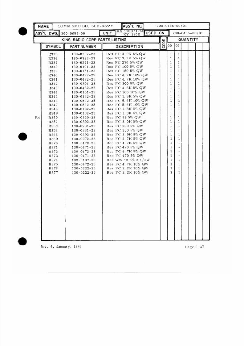
8/9/2019 KX 170A - Maintenance Manual Honeywell
http://slidepdf.com/reader/full/kx-170a-maintenance-manual-honeywell 522/586
R‘
KING RADIO CORI? PARTS LISTING
R335
R336
R337
R338
R339
R340
R341
R342
R343
R344
R345
R346
R34 7
R348
R34 9
R350
R352
R353
R354
R368
R369
R370
R371
R372
R373
R374
R375
R376
R377
PART NUMBER
130-0392-23
130-0332-23
130-0271-23,
130-0101-23
130-0151-23
130-0472-25
130-0472-25
130-0301-23
130-0432-23
130-0101-25
130-0182-23
130-0562-25
130-0562-25
130-0182-23
130-0132-23
130-0820-23
120-0302-23
130-0201-23
130-0331-23
130-0392-23
130-0272-23
130-0472-23
130-0471-23
130-0472-23
130-0471-23
132-0107-30
130-0472-25
130-0222-25
130-0222-25
DESCRIPTION
Res FC 3. 9K 5% QW
Res FC 3. 3K 5’% QW
Res FC 270 5%
QW
Res FC 100 5% QW
Res FC 150 5% QW
Res FC 4. 7K 10% QW
Res FC 4. 7K 10% QW
Res FC 300 5% QW
Res FC 4. 3K 5% QW
Res FC 100 10% QW
Res FC 1. 8K 5% QW
Res FC 5. 6K 10% QW
Res FC 5. 6K 10%
QW
Res FC 1. 8K 5% QW
Res FC 1. 3K 5% QW
Res FC 82 5% QW
Res FC 3. OK 570
QW
Res FC 200 5% QW
Res FC 330 5% QW
Res FC 3. 9K 5%
QW
Res FC 2. 7K 5% QW
Res FC 4. 7K 5% QW
Res FC 470 5% QW
Res FC 4. 7K 5% QW
Res FC 470 5% QW
Res WW 12 5% 3
1/4W
Res FC 4. 7K 10% QW
Res FC 2. 2K 10% QW
Res FC 2. 2K 10% QW
=
0
1
1
1
1
1
1
1
1
1
1
1
1
1
1
1
1
1
1
1
1
1
1
1
1
1
1
1
1
1
I
200-0455-OO/Ol
QUANTITY
Rev. 4, January, 1976
Page 6-37

8/9/2019 KX 170A - Maintenance Manual Honeywell
http://slidepdf.com/reader/full/kx-170a-maintenance-manual-honeywell 523/586
Parts List Revisions Record
Assembly No. 200-0456-OO/Ol (B/MRL Rev. 12 )
ACTION
SYMBOL
PART NUhLZBER
DESCRIPTION
QUANTITY
ADDED
091-0196-00
Spacer 2 2
ADDED
091-0109-00
Plastic Ties 12 12
CHANGE
Q317 007-0113-00
Tstr 2N3646 1 1
CHANGE R350 130-0101-23
Res F/C 1OOR 5% QW 1 1
CHANGE
CHANGE
CHANGE
CHANGE
CHANGE
CHANGE
CHANGE
CHANGE
CHANGE
CHANGE
CHANGE
CHANGE
CHANGE
C322
C328
c350
c351
C356
C369
c377
C378
C381
C562
C567
C568
C569
114-7104-00
114-7104-00
114-7104-00
114-7104-00
114-7104-00
114-7104-00
114-71~4-00
114-7104-00
114-71104-00
114-7104-cg
114-7104-00
114-7104-00
114-7104-00
a
Manual Revision No. 4
Cap Cer . lmf f20% X7R 1 1
Cap Cer . lmf +.200/o X7R 1 1
Cap Cer . lmf lt20% X7R 1 1
Cap Cer . lmf rt20% X7R
1 1
Cap Cer . lmf k20%X7R 1 1
Cap Cer . lmf f20% X7R
11.
Cap Cer . lmf f20% X7R
1 1
Cap Cer . lmf f20% X7R
1 1
Cap Cer . lmf*20% X7R
1 1
Cap Cer . lmf rt20% X7R
1 1
Cap Cer . lmf *20% X7R 1 1
Cap Cer . lmf rt20% X7R 1 -
Cap Cer . lmf +20% X7R
1 -
Page 6-38
Rev. 4, January, 1976

8/9/2019 KX 170A - Maintenance Manual Honeywell
http://slidepdf.com/reader/full/kx-170a-maintenance-manual-honeywell 524/586
SYMBOL
KING RADIO CORl? PARTS LISTING
PART NUMBER
200-0455-00
200-0455-01
016-1011-00
047-1736-02
076-0165-09
076-0343-00
089-5874-03
089-5878-05
091-0087-00
200-0456-00
200-0456-01
DESCRIPTION
=
01
X
X
LR
1
1
1
6
1
1
1
55-OO/Ol
= =
I
-
‘\.
I
11
1
1
1
6
1
1
1
=
KX 175B/KY 195B
ES 170B
Pliobond
Tray Comm SMO
Spacer
Spacer
3cr 2-56 x 3116 PHP
kr 4-40 x 5/16 PHP
hsulation Comm SMO
Comm SMO Sub-Assly
Comm SMO Sub-Assly
February,, 1973 Page 6-39

8/9/2019 KX 170A - Maintenance Manual Honeywell
http://slidepdf.com/reader/full/kx-170a-maintenance-manual-honeywell 525/586
Parts List Revisions Record
I
Assembly No.
200-0455-OO/Ol
ACTION
SYMBOL PART NUMBER
Manual Revision No. 0
DESCRIPTION QUANTIT
Page 6-40
u
February, 1973
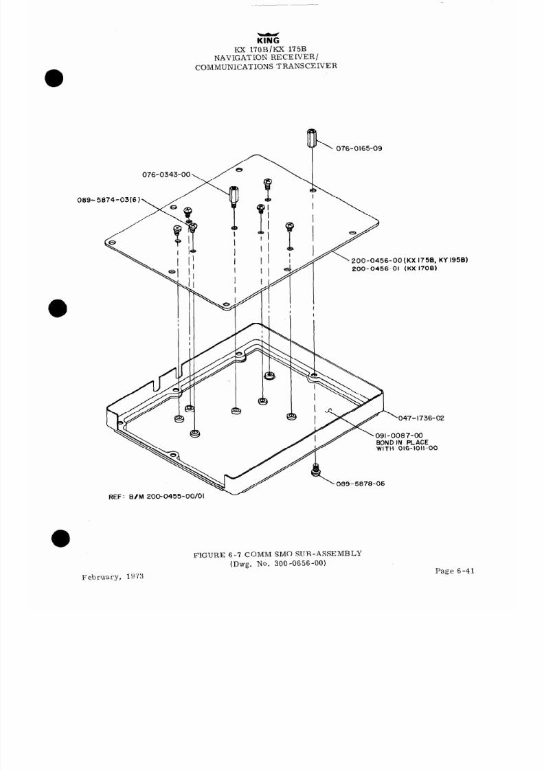
8/9/2019 KX 170A - Maintenance Manual Honeywell
http://slidepdf.com/reader/full/kx-170a-maintenance-manual-honeywell 526/586
089-
KlNG
Io( l?OB/KX 175B
NAVIGATION RECEIVER/
COMMUNICATIONS TRANSCEIVER
076-0165-09
076-0343-00 \
200-0456-00 (KX 1758, KY
200-0456-01 (KX 1708)
\
047- 1736-02
091-0087-00
BOND IN PLACE
WITH 016-1011-00
089-5878-05
REF : B/M 200-0455-OO/Ol
1958)
February, 1973
FIGURE 6 -7 COMM SMO SUB-ASSEMBLY
(Dwg. No. 300 -06 56 -00)
Page 6-41
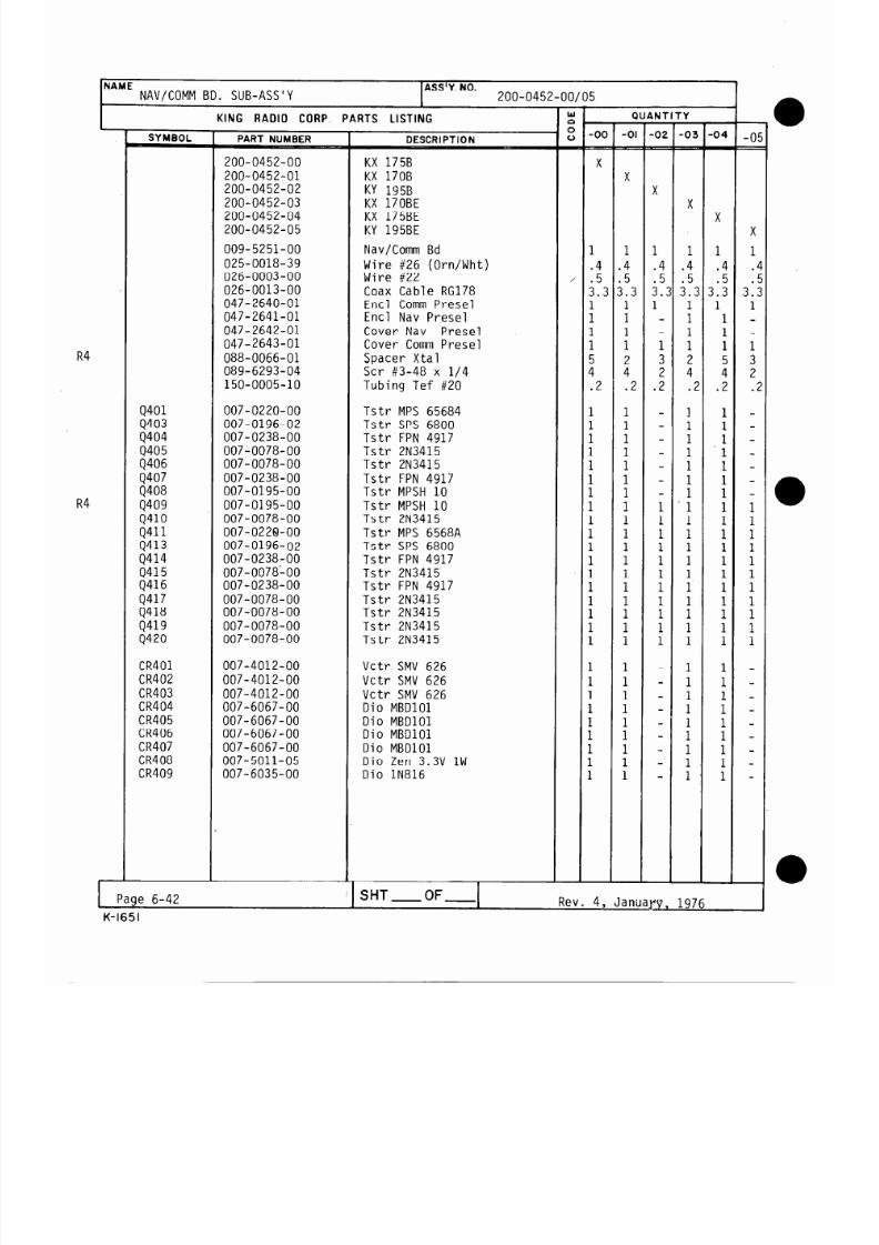
8/9/2019 KX 170A - Maintenance Manual Honeywell
http://slidepdf.com/reader/full/kx-170a-maintenance-manual-honeywell 527/586
NAME
NAV/COMM BD. SUB-ASS'Y
ASS’Y. NO.
ZOO-0452-00/05
L
KING RADIO CORP. PARTS LISTING
SYMBOL
PART NUMBER
DESCRIPTION
200-0452-00
KX 175B
200-0452-01
KX 1708
200-0452-02 KY 195B
200-0452-03
KX 170BE
200-0452-04
KX 175BE
200-0452-05
KY 195BE
009-5251-00
Nav/Comm Bd
025-0018-39
Wire 5126 (Orn/Wht)
026-0003-00
Wire 5122
026-0013-00
Coax Cable RG178
047-2640-01
Encl Comm Presel
047-2641-01
Encl Nav Presel
047-2642-01
Cover Nav Presel
047-2643-01
Cover Comm Presel
088-0066-01 Spacer Xtal
089-6293-04 Scr #3-48 x l/4
150-0005-10
Tubing Tef 5120
4401
4403
Q404
Q405
4406
Q407
4408
Q409
4410
Q411
Q413
Q414
4415
Q416
Q417
Q418
;44:;
007-0220-00
Tstr MPS 65684
007-0196-02
Tstr SPS 6800
007-0238-00
Tstr FPN 4917
007-0078-00
Tstr 2N3415
007-0078-00
Tstr 2N3415
007-0238-00
Tstr FPN 4917
007-0195-00
Tstr MPSH 10
007-0195-00
Tstr MPSH 10
007-0078-00 Tstr 2N3415
007-0228-00
Tstr MPS 6568A
007-0196-02
Tstr SPS 6800
007-0238-00
Tstr FPN 4917
007-0078~00
Tstr 2N3415
007-0238-00
Tstr FPN 4917
007-0078-00 Tstr 2N3415
007-0078-00
Tstr 2N3415
007-0078-00
Tstr 2N3415
007-0078-00
Tstr 2N3415
CR401
007-4012-00
Vctr SMV 626
CR402 007-4012-00
Vctr SMV 626
CR403
007-4012-00
Vctr SMV 626
CR404 007-6067-00
Dio MBDlOl
CR405
007-6067-00
Dio MBDlOl
CR406 007-6067-00
Dio MBDlOl
CR407
007-6067-00
Dio MBDlOl
CR408
007-5011-05
Dio Zen 3.3V 1W
CR409
007-6035-00
Dio lN816
l-
-
-0c
3
X
1
.4
.5
3' .
:
1
1
5
4
.2
1
1
1
t
1
1
1
1
1
1
1
1
1
1
1
1
1
1
1
1
1
1
1
1
1
1
-
R4
R4
1 Paoe 6-42
QUANl rtT
-
-01
-
X
1
4
5
1.3
:
1
1
i
.2
1
1
1
1
1
1
:
1
1
1
:
1
1
1
1
1
1
1
1
1
1
1
1
1
1
-
-
-02
-
X
1
.4
.5
3.
1
I
3
.:
I
1
1
1
1
1
1
1
1
1
1
-
‘Y
-
-02
=
X
1
.4
.5
3
. ~
:
1
:
4
. d
1
1
:
1
1
:
1
1
1
1
:
:
1
1
1
1
1
1
1
1
1
1
1
-
-
-04
-
X
1
.4
1:;
1
1
1
1
5
4
.2
1
1
,1
1
1
:
1
1
1
1
1
1
1
1
1
1
1
1
1
1
1
1
1
1
1
1
-
-
-Of
=
X
1
.l
3:;
1
:
2
.;
I
1
1
1
1
:
1
1
1
1
-
SHT-OF-1
Rev. 4, January, 1976
K-1651

8/9/2019 KX 170A - Maintenance Manual Honeywell
http://slidepdf.com/reader/full/kx-170a-maintenance-manual-honeywell 528/586
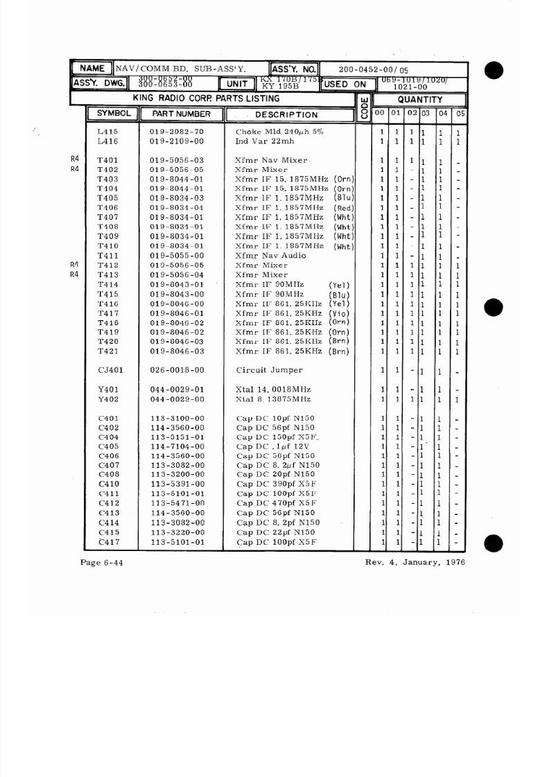
8/9/2019 KX 170A - Maintenance Manual Honeywell
http://slidepdf.com/reader/full/kx-170a-maintenance-manual-honeywell 529/586
R4
R4
R4
R4
SYMBOL
KING RADIO CORI? PARTS LISTING
L415
L416
T401
T402
T403
T404
T405
T406
T407
T408
T409
T410
T411
T412
T413
T414
T415
T416
T417
T418
T419
T420
T421
CJ40 1
Y401
Y402
c401
C402
c404
c405
C406
c407
C408
c410
C411
C412
C413
c414
c415
i7417
PART NUMBER
01 g-2082-70
019-2109-00
01 g-5056-03
019-5056-05
019-8044-01
019-8044-01
019-8034-03
019-8034-04
019-8034-01
019-8034-01
019-8034-01
019-8034-01
019-5055-00
01 g-5056-05
01 g-5056-04
019-8043-01
019-8043-00
019-8046-00
019-8046-01
019-8046-02
019-8046-02
019-8036-03
019-8046-03
026-0018-00
044-0029-01
044-0029-00
113-3100-00
114-3560-00
113-5151-01
114-7104-00
114-3560-00
113-3082-00
113-3200-00
113-5391-00
113-5101-01
113-5471-00
114-3560-00
113-3082-00
113-3220-00
113-5101-01
DESCRIPTION
Choke Mld 240ph 5%
Ind Var 22mh
Xfmr Nav Mixer
Xfmr Mixer
Xfmr IF 15. 1875MHz
(Orn
Xfmr IF 15. 1875MHz
(Orn
Xfmr IF 1. 1857MHz
(Blu
Xfmr IF 1. 1857MHz
(Red
Xfmr IF 1. 1857MHz
(Wht
Xfmr IF 1. 1857MHz (Wht
Xfmr IF 1. 1857MHz
(Wht
Xfmr IF 1. 1857MHz
(Wht
Xfmr Nav Audio
Xfmr Mixer
Xfmr Mixer
Xfmr IF 9OMHz
Xfmr IF 9OMHz
Xfmr IF 861. 25KHz (Ye1 )
Xfmr IF 861. 25KHz (Vio)
Xfmr IF 861. 25KHz (orn)
Xfmr IF 861. 25KHz
(Orn)
Xfmr IF 861. 25KHz
(Brn)
Xfmr IF 861. 25KHz
(Brn)
Circuit Jumper
Xtal 14. 0018MHz
Xtal 8. 13875MHz
Cap DC 10pf N150
Cap DC 56pf N150
Cap DC 150pf X5F-
Cap DC .lpf 12V
Cap DC 56pf N150
Cap DC 8. 2pf N150
Cap DC 20pf N150
Cap DC 390pf X5F
Cap DC 1OOpf X5F
Cap DC 470pf X5F
Cap DC 56pf N150
Cap DC 8. 2pf N150
Cap DC 22pf N150
Cap DC 1OOpf X5F
00
-
1
1
1
1
1
1
1
1
1
1
1
1
1
1
1
1
1
1
1
1
1
1
1
1
1
1
1
1
1
1
1
1
1
1
1
1
1
1
1
1
E
1
1
1
1
1
1
1
1
1
1
1
1
1
1
1
1
1
1
1
1
1
1
1
1
1
1
1
1
1
1
1
1
1
1
1
1
1
1
1
1
=
02
1
1
1
1
1
1
1
1
1
1
1
1
1
1
03-
1
1
1
1
1
1
1
1
1
i
1
1
1
:
1
1
1
1
1
1
1
1
1
1
1
1
%
L
i
Fi
1
1
1
1
1
1
1
1
1
1
1
1
1
1
:
1
:
1
1
1
1
1
1
1
1
1
1
t
1
1
1
1
1
1
1
1
=
O
1
1
Page 6-44
Rev. 4, January, 1976
-
l

8/9/2019 KX 170A - Maintenance Manual Honeywell
http://slidepdf.com/reader/full/kx-170a-maintenance-manual-honeywell 530/586
R4
R4
SYMBOL
KING RADIO CORF PARTS LISTING
C418
c419
C420
C421
C422
C424
C425
C426
C428
c429
c435
C436
c437
C438
C4 3 9
c440
C44 1
C442
c44 3
c444
C446
c447
C448
c-449
c450
c451
C452
c453
C454
c455
C456
c457
C458
c459
C460
C461
C462
C463
C464
C465
C466
C467
c‘468
C469
PART NUMBER
106-0001-18
106-0001-34
114-7104-00
114-7104-00
113-7203-00
106-0001-34
114-7104-00
114-7104-00
106-0001-34
114-7104-00
096-1030-24
114-7104-00
105-0031-08
113-7503-00
097-0062-02
097-0062-06
096-1030-25
096-1030-25
096-1030-08
113-7503-00
113-7503-00
113-5181-00
113-3330-00
113-7503-00
114-7104-00
114-7104-00
096-1030-24
096-1030-17
114-7104-00
105-0031-47
114-7104-00
096-1030-03
113-7503-00
114-7104-00
113-5331-00
114-7104-00
114-7104-00
1133270 -00
096-1030-17
097-0062-06
097-0062-06
113-3039-00
113-3820-00
113-3047-00
DESCRIPTION 1
CapMld . 82pf 50/o
CapMld 6. 8pf 5%
Cap DC . lpf 12V
Cap DC . lpf 12V
Cap DC. 02pf 12V
Cap M ld 6. 8pf 5%
Cap DC . lpf 12V
Cap DC . lpf 12V
Cap M ld 6. 8pf 5%
Cap DC . ll.tf 12V
Cap Tant 68pf 1OV
Cap DC . lpf 12V
Cap Myl.
. 0022pf 80V
Cap DC . 05pf 12V
Cap Elec , 22pf 25V
Cap Elec l/*f 25V
Cap Tant 150pf 1OV
Cap Tant 150pf 1OV
Cap Tant 100pf 15V
Cap DC , 05pf 12V
Cap DC . 05pf 12V
Cap DC 180pf X5F
Cap DC 33pf N150
Cap DC . 05pf 12V
Cap DC . lpf 12V
Cap DC . ll.tf 12V
Cap Tant 68pf 1OV
Cap Tant 6. 8pf 15V
Cap DC . lpf 12V
Cap My1 . 0271.tf 8OV
Cap DC . lpf 12V
Cap Tant 2. 2pf 15V
Cap DC . 05pf 12V
Cap DC . lpf 12V
Cap DC 330pf X5F
Cap DC . lpf 12V
Cap DC . lyf 12V
Cap DC 27pf N150
Cap Tant 6. 8yf 15V
Cap Elec lpf 25V
Cap Elec l/*f 25V
Cap DC 3. 9pf N150
Cap DC 82pf X5F
Cap DC 4.7pf N150
‘069:
L-
102
=
10
T
1
1
1
1
1
1
1
1
1
1
1
1
1
1
1
1
1
1
1
1
1
1
1
1
1
1
1
1
1
1
1
1
1
1
1
1
1
1
1
1
1
1
1
c
E
7
1
1
1
1
1
1
1
1
1
1
1
1
1
1
1
1
1
1
1
1
1
1
1
1
1
1
1
1
1
1
1
1
1
1
1
1
1
1
1
1
1
1
1
1019/1020/
l-00
IANTITY
1
1
1
1
1
1
1
1
1
1
Rev. 4, January, 1976
Page 6-45

8/9/2019 KX 170A - Maintenance Manual Honeywell
http://slidepdf.com/reader/full/kx-170a-maintenance-manual-honeywell 531/586
NAME 11 NAV/COMM BD. SUB-ASS’Y.
IIASS’Y. NdI
200-0452-00/1x
SYMBOL
PART NUMBER
c470 113-5151-01
C472
114-7104-00
c473 113-5151-01
c4 74
113-5022-00
(‘4 75 113-3390-00
C476
113-5471-00
c477 113-5471-00
C478
113-5151-01
c479 113-5151-01
C480 113-5151-01
(‘4 8 1 113-3015-00
C482 113-3270-00
C483 113-3820-00
C484 106-0001-36
C485 114-7104-00
C486 114-7104-00
C487 106-0001-37
C488 114-7104-00
C489 114-7104-00
c490 113-7203-00
C491
106-0001-36
c492 114-7104-00
c493 114-7104-00
c4 94 114-7104-00
c495 096-1030-27
C4 96 105-0031-32
c497 096-1030-27
C498 097-0062-06
c499 097-0062-06
c501 114-7104-00
C502 105-0031-35
c503 105-0031-32
c504 113-3820-00
C505 096-1030-21
C506 114-7104-00
c507 113-7203-00
C508 096-1030-27
c509
097-0062-06
C510 113-7203-00
c511
097-0062-06
C512 096-1030-21
c513
114-7104-00
c514
105-0031-63
c515 114-7104-00
KING RADIO CORF PARTS LISTING
Page 6-46
DESCRIPTION
Cap DC 150pf X5F
Cap DC . lpf 12V
Cap DC 150pf X5F
Cap DC 2. 2pf N150
Cap DC 39pf N150
Cap DC 470pf X5F
Cap DC 470pf X5F
Cap DC 150pf X5F
Cap DC 150pf X5F
Cap DC 150pf X5F
Cap DC 1. 5pf N150
Cap DC 27pf N150
Cap DC 82pf X5F
Cap M ld 5. 6pf 50 /o
Cap DC . lpf 12V
Cap DC . lyf 12V
Cap M ld 6. 2pf 5%
Cap DC . lpf 12V
Cap DC . lpf 12V
Cap DC . 02pf 12V
Cap Mld 5. 6pf 5 %
Cap DC . lpf 12V
Cap DC lpf 12V
Cap DC . lpf 12V
Cap Tant 15pf 15V
Cap My1 . Olpf 80V
Cap Tant 15yf 15V
Cap Elec lpf 25V
Cap Elec lpf 25V
Cap DC lpf 12V
Cap My1 . 012pf 80V
Cap My1 , Olyf 8OV
Cap DC 82pf X5F
Cap Tant 12pf 1OV
Cap DC lpf 12V
Cap DC . 02pf 12V
Cap Tant 15pf 15V
,Cap Elec lpf 25V
Cap DC . 02pf 12V
Cap Elec lpf 25V
Cap Tant 12pf 1OV
Cap DC . lpf 12V
Cap My1 . 068pf 80V
Cap DC . lpf 12V
QUANTITY
z
1
1
1
1
1
1
1
1
1
1
1
1
1
1
1
1
1
1
1
1
1
1
1
1
1
1
1
1
1
1
1
1
1
1
1
1
1
1
1
1
1
1
1
1
G
1
1
1
1
1
1
1
1
1
1
1
1
1
1
1
1
1
1
1
1
1
1
1
1
1
1
1
1
1
1
1
1
1
1
1
1
1
1
1
1
1
1
1
1
=
3;
1
1
1
1
1
1
1
1
1
1
1
1
1
1
1
1
1
1
1
1
1
1
1
1
1
1
1
1
1
1
1
1
1
1
1
1
1
1
1
1
1
1
1
1
Rev. 4, January, 1976
=
O
i
1
1
1
1
1
1
1
:
1
1
1
1
:
1
1
1
1
1
1
1
1
:
1
1
1
1
1
1
1
1
1
:
1
1
1
:
:

8/9/2019 KX 170A - Maintenance Manual Honeywell
http://slidepdf.com/reader/full/kx-170a-maintenance-manual-honeywell 532/586
R4
R4
SYMBOL
KING RADIO CORP PARTS LISTING
C516
C517
1401
1402
1403
1404
1405
R401
R402
R403
R404
R405
R406
R407
R408
R409
R410
R413
R414
R415
R417
R421
R422
R424
R425
R426
R427
R428
R429
R430
R431
R432
R433
R434
R435
R436
R437
R438
R439
R440
R441
R442
PART NUMBER
106-0001-15
106-0001-15
120-3007-00
120-3007-00
120-3006-00
120-3007-00
120-3007-00
130-0103-25
130-0103-25
130-0102-23
130-0622-23
130-0621-23
130-0101-25
130-0103-25
130-0473-23
130-0683-23
130-0222-23
130-0131-23
130-0132-23
130-0332-23
130-0473-23
130-0103-25
130-0473-23
130-0201-23
133-0084-01
130-0471-25
130-0112-23
130-0242-23
130-0103-23
130-0222-23
130-0223-23
130-0223-23
136-1741-77
136-1211-77
130-0181-23
130-0222-25
130-0331-23
130-0101-25
130-0101-25
130-0512-23
130-0133-23
130-0472-23
DESCRIPTION ~4
Cap Mld . 56pf 10%
Cap Mld . 56pf 10%
IC U8B7703394
IC U8B7703394
IC CA3020
IC U8B7703394
IC U8B7703394
Res FC 10K 10% QW
Res FC 10K 10% QW
Res FC 1K 50/ QW
Res FC 6. 2K
570
QW
Res FC 620 5’70 QW
Res FC 100 10% QW
Res FC 10K 10% QW
Res FC 47K 5% QW
Res FC 68K 5To QW
Res FC 2. 2K 5% QW
Res FC 130 5% QW
Res FC 1. 3K 5% QW
Res FC 3. 3K 5% QW
Res FC 47K 5% QW
Res FC 10K 10% QW
Res FC 47K50/o Q W
Res FC 200 5% QW
Res Var 5K
Res FC 470 10% QW
Res FC 1. 1K 5% QW
Res FC 2.4K 5% QW
Res FC 10K 5% QW
Res FC 2. 2K 5% QW
Res F‘C 22K 5% QW
Res FC 22K 5% QW
Res 1. 74K 1%
Res 1. 21K 1%
Res FC 180 5% QW
Res FC 2. 2K 10% QW
Res FC 330 5% QW
Res FC 100 10% QW
Res FC 100 10% QW
Res FC 5. IK 5% QW
Res FC 13K 5% QW
Res FC 4. 7K 57’0 QW
069-1019/1020/
1021-00
F
-i
1
1
1
1
1
1
1
1
1
1
1
1
1
1
1
1
1
1
1
1
1
1
1
1
1
1
1
1
1
1
1
1
1
1
1
1
1
1
1
1
1
QUANTITY
E
1
1
1
1
1
1
1
1
1
1
1
1
1
1
1
1
1
1
1
1
1
1
1
1
1
1
1
1
1
1
1
1
1
1
1
1
1
1
1
1
=
03-
1
1
1
1
1
1
1
1
1
1
:
1
1
1
1
1
1
1
1
1
1
1
1
1
1
1
1
1
1
1
1
1
1
1
1
1
1
1
1
-
E
1
1
1
1
1
1
1
1
1
1
1
1
1
1
1
1
1
1
1
1
1
1
1
1
1
1
1
1
1
1
1
1
1
1
1
1
1
1
1
1
=
05
-
1
1
February, 1873
Page 6-47

8/9/2019 KX 170A - Maintenance Manual Honeywell
http://slidepdf.com/reader/full/kx-170a-maintenance-manual-honeywell 533/586
R4
R4
R4
R4
R4
R4
SYMBOL
R443
R444
R44 5
R446
R44 7
R448
R449
R450
R451
R452
R453
R454
R455
R456
R457
R458
R460
R461
R462
R463
R464
R465
R466
R467
R468
R469
R470
R471
R472
R473
R4 74
R475
R477
R478
R481
R482
R483
R484
R485
R486
R487
R488
R489
R490
KING RADIO CORI? PARTS LISTING
PART NUMBER
130-0132-23
130-0300-33
130-0224-25
130-0224-25
130-0152-25
130-0751-23
130-0182-23
130-0224-23
130-0472:23
130-0202-23
130-0133-23
130-0512-23
130-0101-25
130-0470-25
130-0102-23
130-0753-23
130-0103-25
130-0103-25
130-0102-23
130-0751-23
130-0682-23
130-0101-25
130-0103-25
130-0103-25
130-0274-25
130-0154-23
130-0222-23
130-0184-23
130-0184-23
130-0131-23
130-0911-23
130-0272-23
130-0134-23
130-0164-23
‘130-0103-25
130-0330-23
133-0084-02
130-0181-23
130-0681-23
130-0391-23
130-0473-25
130-0103-23
130-0472-23
130-0152-23
DESCRIPTION
Res FC 13K 5% QW
Res FC 30 5% HW
Res FC 220K 10% QW
Res FC 220K 10% QW
Res FC 1. 5K 10% QW
Res FC 750 57’0QW
Res FC 1. 8K 5% QW
Res FC 220K 5% QW
Res FC 4. 7K 5% QW
Res FC 2. OK 5% QW
Res FC 13K
57’0
QW
Res FC 5. 1K 5% QW
Res FC 100 10% QW
Res FC 47 1070 QW
Res FC 1K 5To QW
Res FC 75K 5% QW
Res FC 10K 10% QW
Res FC 10K 10% QW
Res FC 1K
570
QW
Res FC 750 5% QW
Res F‘C 6. 8K5% QW
Res E‘C 100 10% QW
Res FC 100 10% QW
Res FC 100 10% QW
Res FC 270K 10% QW
Res F‘C 150K 5% QW
Res FC 2. 2K
570
QW
Res FC 180K 5070QW
Res FC 180K 5% QW
Res FC 130 5% QW
Res FC 910
57’0
QW
Res FC 2. 7K 5% QW
Res FC 130K 5% QW
Res FC 160K 5% QW
Res FC 10K 10% QW
Res FC 33 570 QW
Res Var 10K
Res FC 180 5% QW
Res F’C 680 5% QW
Res FC 390 5% QW
Res E‘C 47K 10% QW
Res F‘C 10K 5% QW
Res FC 4. 7K 5% QW
Res F’C 1. 5K 5% QW
cc?
02
t
= = =
30 01 02
F
04 05
-
1 1
i-
i-
1 1
1
1
1 1
1
1
1 1 1 1
1 1
1
1
1 1
1
1
1 1
1
1
1 1
1
1
1 1 1
1
1 1
1 1 1
1 1
1
1 1
1
1
1 1
1 1 1
1 1 1
1 1 1 1 1 1
1 1 1
1 1 1
1 1 1
1
:
1
1 1
1
1 1
1 1
1
1 1 1
1 1 1
1 1 1
1 1 1
1
1
1
1 1 1
1 1 1
1 1 1
1 1 1
1 1
1
1 1 1
1 1 1
1
1
1
1 1
1
1 1
1
1 1 1 1 1 1
1 1 1
1
1
1
1 1 1
1 1 1
1 1 1 1
1
1
1 1 1
1
1
1
1 1 1
1
1 1
1 1 1
1 1 1
1 1
1
1
1 1
1 1 1
1
1 1
1 1
1
1
1
1
1 1 1
1
:
1
1 1 1
1
1
1 1
1
1 1 1
1 1 1 1 1 1
1 1 1
1
1
1
1 1
1
1
1
1
1 1 1
1
1 1
1
t
1
:
1 1
1
1
1
1
1 1
1
1 1 1
I
-
JANTITY
Page 6-48
Rev. 4, January, 1976

8/9/2019 KX 170A - Maintenance Manual Honeywell
http://slidepdf.com/reader/full/kx-170a-maintenance-manual-honeywell 534/586
KING RADIO CORl? PARTS LISTING
R491
R492
R493
R4 94
R495
R496
R497
R498
R499
R500
R501
R502
R503
R504
R505
R,506
R507
R508
R509
R510
RT501
RT502
PART NUMBER
130-0222-25
130-0472-23
130-0331-23
130-0621-23
133-0084-00
130-0182-23
130-0181-25
130-0473-25
130-0101-25
130-0102-25
130-0184-25
130-0471-25
130-0101-25
130-0182-23
130-0102-25
130-0103-23
130-0103-23
130-0332-23
130-0103-23
130-0271-25
134-1004-00
134-1819-00
DESCRIPTION
I
Res FC 2. 2K 10% QW
Res FC 4. 7K 5% QW
Res FC 330 5% QW
Res FC 620 5% QW
Res Var 1K
Res FC 1. 8K 5% QW
Res FC 180 10% QW
R.es FC 47K 10% QW
Res FC 100 10% QW
Res FC 1K 10% QW
Res FC 180K 10% QW
Res FC 470 10% QW
Res FC 100 10% QW
Res FC 1. 8K 5% QW
Res FC 1K 10% QW
Res FC 10K 5% QW
Res FC 10K 5% QW
Res FC 3. 3K 5% QW
Res FC 10K 5% QW
Res FC 270 10% QW
Tmtr 1K
Tmtr 50
QUANTITY
=
02
'i
1
1
1
1
1
1
1
1
1
1
1
1
1
1
1
1
1
1
1
1
34
i-
1
1
1
1
1
1
1
1
1
1
1
1
1
1
1
1
1
1
1
1
=
OE
T
1
1
1
1
1
1
1
1
1
1
1
1.
1
1
1
1
1
1
1
1
February, 1973
Page 6-49

8/9/2019 KX 170A - Maintenance Manual Honeywell
http://slidepdf.com/reader/full/kx-170a-maintenance-manual-honeywell 535/586
Parts List Revisions Record
Assembly No. 200-0452-00/05 (B/MRL Rev 18)
ACTION
CHANGE
ADDED
CHANGE
CHANGE
DELETE
CHANGE
ADDED
DELETE
CHANGE
CHANGE
CHANGE
CHANGE
ADDED
CHANGE
CHANGE
CHANGE
CHANGE
ADDED
ADDED
CHANGE
CHANGE
CHANGE
CHANGE
CHANGE
ADDED
Page 6-50
SYMBOL
CR426
R488
L406
R450
R511
c455
c454
4409
R452
CR2410
FL403
T401
T402
T412
T413
C482
C483
R433
RQ34
R443
R466
R467
c471
PART NUMBER DESCRIPTION
088-0066-00
047-1943-00
007-6059-00
130-0512-23
019-2019-00
130-0474-23
130-0331-23
105-0031-47
111-0001-03
007-‘0196-02
130-0362-23
007-6035-03
017-0034-00
019-8066-00
019-8066-00
019-8066-00
019-8066-00
113-3390-00
113-5101-01
136-1741-72
136-1211-72
130-0332-23
130-0103-25
130-0103-25
113-3027-00
Manual Revision No. 4
Spacer; Xtal
Spring, Clip
Diode FD400
Res F/C 5.1K 5% QW
Res F/C 470K 5% QW
Res F/C 330 ohm 5% QW
Cap MC .22uf
Tstr SPS6800
Res F/C 3.6K 5% QW
Dio lN816
Fil 9.00MHz
Xfmr Nav Mixer
Xfmr Mixer
Xfmr Mixer
Xfmr Mixer
Cap D/C 39pf N150
Cap D/C 1OOpf X5F
Res 1.74K 1%
Res 1.21K 1%
Res F/C 3.3K 5% QW
Res F/C 10K 10% QW
Res F/C 10K 10% QW
Cap D/C 2.7pf N150
QUANTITY
00 01 02
03 04 05
5 2 3
2 5 3
1 l--l1
: 1 1 1 1 1
1 1
1 1 1
1 1 - 1 1 -
1 1 - 1 1 -
1 1 - 1 1 -
1 1 1 1 1 1
1 1 1 1 1 1
1 l-111
11 1
i Xii-
1 l-ll-
1 1 1 1 1 1
1 1 1 1 1 1
- -- 1 - -
; ; I : ; :
1 1 - 1 1 -
1 l-ll-
1 1 1 1 1 1
1 1 1 1 1 1
- -- 1 1 1
.-
Rev. 4, January, 1976

8/9/2019 KX 170A - Maintenance Manual Honeywell
http://slidepdf.com/reader/full/kx-170a-maintenance-manual-honeywell 536/586
SYMBOL
KING RADIO CORF PARTS LISTING
CR60 1
CR602
L601
T60 1
T602
T603
C601
C602
C603
C604
C605
C606
C607
C608
C609
C610
C613
C614
C615
C6 16
C6 17
C618
C6 19
C620
C621
C622
C628
PART NUMBER
009-5075-00
026-000 l-00
026-0003-00
150-0003-10
150 -0042 - 10
007-0195-00
007-6022-00
007 -6022 -00
0 19-2057-11
0 19-3044 -00
0 19-3026-00
019-3026-00
113-5471-00
113-3180-00
113-5471-00
113-3120-00
113-5151-01
106-0034-00
113-6103-00
106-0034-00
113-3390-00
102-0024-09
113-6103-00
113-6103-00
106-0034-00
113-3820-00
113-3820-00
113-3680’-00
102-0024-09
113-6103-00
106-0034-00
102-0024-09
113-6103-00
DESCRIPTION
P.A. Board
#26 Buss Wire
#22 Buss Wire
Tubing Teflon #24
Shrink Tubing
.Tstr MPS-H 10
Dio Ts-6
Dio Ts-6
Choke .82ph 5%
Tfmr R. F. Buffer
Tfmr R. F.
Tfmr R. F.
Cap DC 470pf 10%
Cap DC 18pf 500V
Cap DC 470pf 10%
Cap DC 12pf 5%
Cap DC 150pf 10%
Cap FT 1. 5Kpf
Cap DC . Olpf
Cap FT 1. 5Kpf
Cap DC 39pf 5%
Cap VAR 7-35pf
Cap DC .Olpf
Cap DC .Olpf
Cap FT 1.5Kpf
Cap DC 82pf 5%
Cap DC 82pf 5%
Cap DC 68pf 500V
Cap VAR 7-35pf
Cap DC .Olpf
Cap FT 1. 5Kpf
Cap VAR 7-35pf
Cap DC . Olpf
il
200 -0082 -00
-
O(
-
1
1
1
1
2
1
1
1
1
1
1
1
1
1
1
1
1
1
1
1
1
1
1
1
1
1
1
1
1
1
1
1
1
QUANTITY
=
-
=
-
February, 1973 Page 6-51
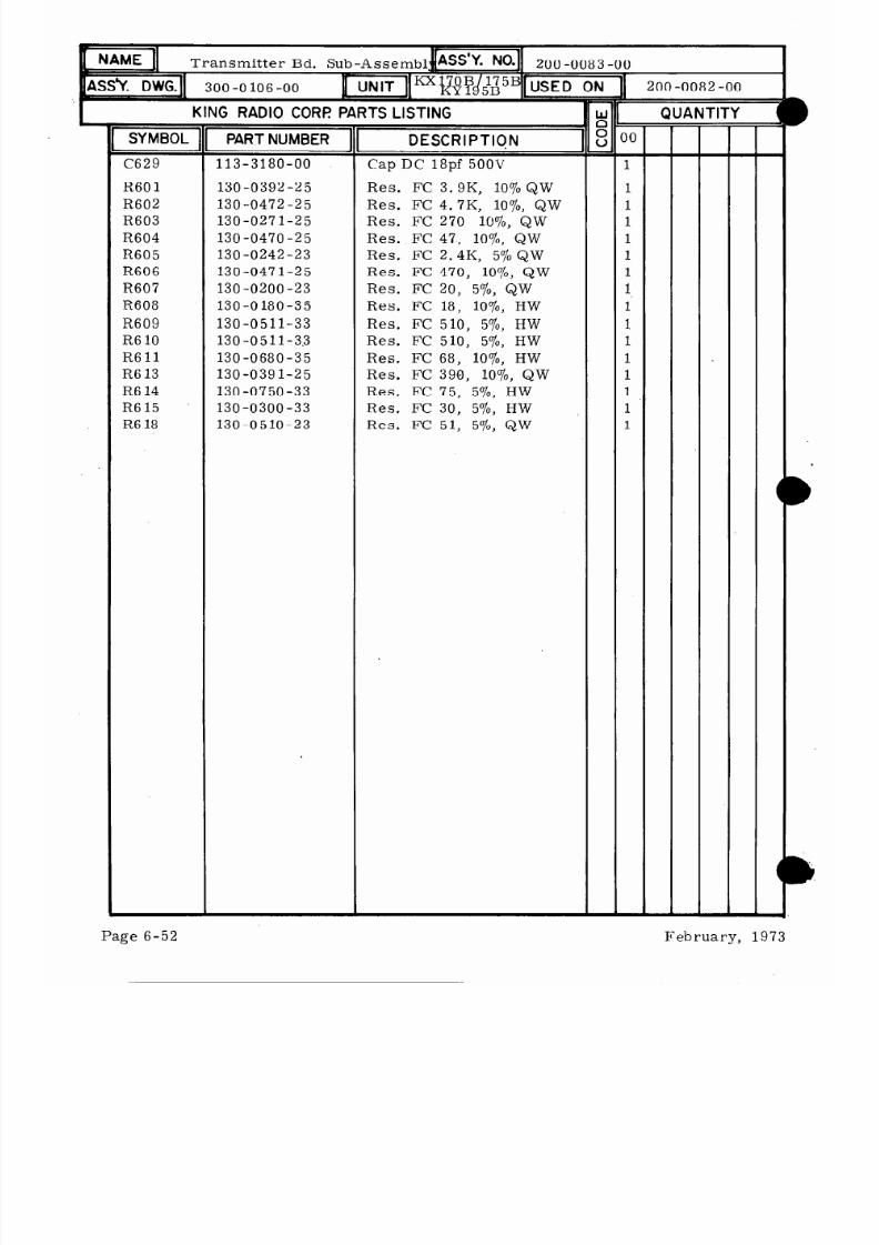
8/9/2019 KX 170A - Maintenance Manual Honeywell
http://slidepdf.com/reader/full/kx-170a-maintenance-manual-honeywell 537/586
SYMBOL]
C629
R60 1
R602
R603
R604
R605
R606
R607
R608
R609
R6 10
R611
R6 13
R6 14
R615
R6 18
KING RADIO CORF PARTS LISTING
Page 6-52
PART NUMBER
113-3180-00
130-0392-25
130-0472-25
130-0271-25
130 -0470 -25
130-0242-23
130-0471-25
130 -0200 -23
130-0180-35
130-0511-33
130-0511-3.3
130-0680-35
130-0391-25
130-0750-33
130-0300-33
130-0510-23
DESCRIPTION
Cap DC 18pf 500V
Res. FC 3. 9K, 10% QW
Res. FC 4. 7K, lo%, QW
Res. FC 270 lo%, QW
Res. FC 47, lo%, QW
Res. FC 2.4K, 5% QW
Res. FC 470, lo%, QW
Res. FC 20, 5%, QW
Res. FC 18, lo%, HW
Res. FC 510, 5%, HW
Res. FC 510, 5%, HW
Res. FC 68, lo%, HW
Res. FC 390, 1070, QW
Res. FC 75,
57’0,
HW
Res. FC
30, 570, HW
Res. FC 51, 5%, QW
0
I
200 -0082 -00
7i
T
1
1
1
1
1
1
1
1’
1
1
1
1
1
1
1
QUANTITY
=
-
=
-
February, 973

8/9/2019 KX 170A - Maintenance Manual Honeywell
http://slidepdf.com/reader/full/kx-170a-maintenance-manual-honeywell 538/586
Parts List Revision Record
Assembly No. 200 -0083 -00
Manual Revision No. 0
ACTION
SYMBOL
PART NUMBER
DESCRIPTION
QUANTITY
February, 1973
Page 6-53

8/9/2019 KX 170A - Maintenance Manual Honeywell
http://slidepdf.com/reader/full/kx-170a-maintenance-manual-honeywell 539/586
NAME
I
KING RADIO CORF PARTS LISTING
Q602 007-0066-00
Tstr 2N3866 -
Q603
007-0149-00
Tstr SS3932
Q604 007-0150-00
Tstr SS3933
CR603
007-6059-00
Dio FD400
CR604
007-6059-00
Dio FD400
FL60 1 ‘.
0 17-0025-00
Filter
FL602
0 17 -0027 -00
Filter
FL603 0 17 -0027 -00
Filter
L604
0 19-2054-17 Choke 1.2,uh 570
T604 0 19 -3045-00
R. F. Tfmr
5172
J 1.73
Ant. Conn.
L
Ant. Conn.
ON
SYMBOL 1
PART NUMBER
008 -0042 -00
008 -0044-O 1
010-0019-90
0 10 -0029 -90
0 16 - 1004-00
026-0003-00
047-1833-01
073 -0093 -02
076-0139-09
076 -0 164-06
089-2005-3’7
089-2272-30
089-5874-03
089-5878-04
089-8012-37
090-0133-00
09 l-0028 -00
09 1-o 155-00
200-0083-00
DESCRIPTION
Lug, Solder
Term. Gnd Stud
Term. Standoff
Term. Feedthru
Thermal Comp
#22 Wire
Cover Conn
Rear Plate
Spat er
Spacer
Nut Hex #2-56
Nut #8 -32
Ser. 2-56X3 /lS PHP
Ser. 4-40X1 /4 PHP
Washer #2
Heat Sink
Ser. Nyl 4-40X3 / 16
Washer, Mica
Trans. Bd. Sub-Ass’y.
1
1
2
1
AF
1
1
1
1
3
1
2
3
2
1
1
1
1
1
1
1
1
1
1
1
1
1
1
1
1
1
QUANTITY
=
-
Page 6-54
February, 1973

8/9/2019 KX 170A - Maintenance Manual Honeywell
http://slidepdf.com/reader/full/kx-170a-maintenance-manual-honeywell 540/586
Rear Plate
Sub-Assembly
200-0082-00
IIASS’Y. DWG.11 300-0105-00’
11
UN IT 11W-Y ? TY3
KING RADIO CORP PARTS LISTING
SYMBOL] PART NUMBER
DESCRIPTION
1;
C611
106-00 18 -0 1
C6 12 106 -00 18 -0 1
C623
113-3121-00
C624
106-0006-02
C625
113-5221-01
C626 106-0006-03
C627
106-0006-00
C629
106-0006-00
C631
106-0024-00
C632
113-3200-00
R6 12
R6 16
R617
130 -0068 -33 Res FC 6.8570 HW
130-0222-25
Res FC 2.2K 10% QW
130-0471-35 Res FC 470 10% HW
Cap FT 1.5Kpf
Cap FT 1.5Kpf
Cap DC 120pf 5%
Cap FT 22pf
Cap DC 220pf 10%
Cap FT 250pf
Cap FT 33pf
Cap FT 33pf
Cap Standoff 20pf
Cap DC 20pf 5’7’0
QUANTITY
=
00
-
1
1
1
1
1
1
1
1
1
1
1
1
1
=
February, 1973
Page 6-55

8/9/2019 KX 170A - Maintenance Manual Honeywell
http://slidepdf.com/reader/full/kx-170a-maintenance-manual-honeywell 541/586
Parts List Revision Record
Assembly No. 200 -0082 -00
Manual Revision No. 0
ACTION’
SYMBOL
PART NUMBER
DESCRIPTION QUANTITY
0
Page 6-56
February, 1973

8/9/2019 KX 170A - Maintenance Manual Honeywell
http://slidepdf.com/reader/full/kx-170a-maintenance-manual-honeywell 542/586
c629 (REF)
CR604
.603
t631
<
?706
-
T604
‘-..
C623(
.b.
.M 9 TO
ITEM9 I:. 2(3
‘0
0602
NOTES:
I. BALLOON NO’s REFER TO ITEM No’s ON B/M 200-0082-00.
,.“P” NO’s ARE FOR REF. TO POINT T O POINT WIRING CONN.
/A 3. TORQUE REQUIREMENTS- go-looiN. oz. (ITEM 2 8 3).
February, 1973
FIGURE 8 REAR PLA’I’E YUB-XYY~IVI~~LY
(Dwg. No. 300-0105-00)
Page 6-568
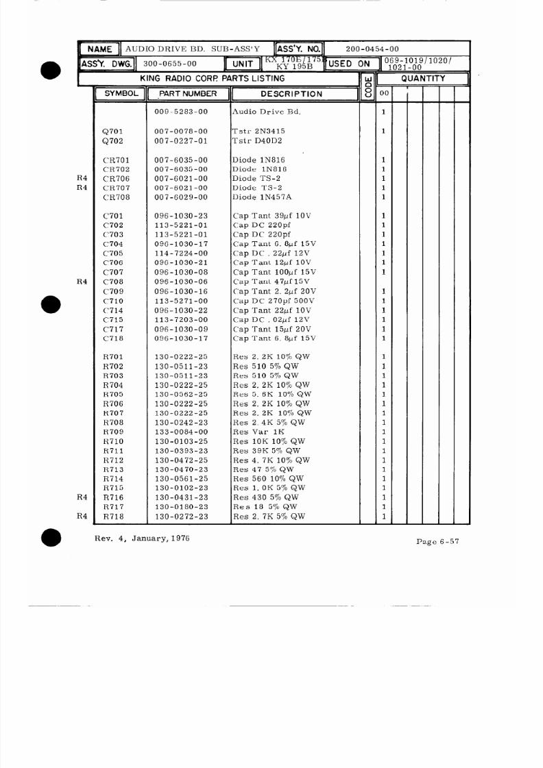
8/9/2019 KX 170A - Maintenance Manual Honeywell
http://slidepdf.com/reader/full/kx-170a-maintenance-manual-honeywell 543/586
R4
R4
R4
R4
R4
SYMBOL
Q701
Q702
CR701
CR702
CR706
CR707
CR708
C701
C702
c703
c704
C705
C706
c707
C708
c709
C710
C714
c715
C717
C718
R701
R702
R703
R704
R705
R706
R707
R708
R709
R710
R711
R712
R713
R714
R715
R716
R717
R718
KING RADIO CORF PARTS LISTING
PART NUMBER
009-5283-00
007-0078-00
007-0227-01
007-6035-00
007-6035-00
007-6021-00
007-6021-00
007-6029-00
096-1030-23
113-5221-01
113-5221-01
096-1030-17
114-7224-00
096-1030-21
096-1030-08
096-1030-06
096-1030-16
113-5271-00
096-1030-22
113-7203-00
096-1030-09
096-1030-17
130-0222-25
130-0511-23
130-0511-23
130-0222-25
130-0562-25
130-0222-25
130-0222-25
130-0242-23
133-0084-00
130-0103-25
130-0393-23
130-0472-25
130-0470-23
130-0561-25
130-0102-23
130-0431-23
130-0180-23
130-0272-23
DESCRIPTION
Audio Drive Bd.
Tstr 2N3415
Tstr D40D2
Diode lN816
Diode lN816
Diode TS-2
Diode TS-2
Diode lN457A
Cap Tant 39pf 1OV
Cap DC 220pf
Cap DC 220pf
Cap Tant 6. 8pf 15V
Cap DC . 22pf 12V
Cap Tant 12yf 1OV
Cap Tant 1OOpf 15V
Cap Tant 47pf 15V
Cap Tant 2. 2pf 20V
Cap DC 270pf 500V
Cap Tant 22pf 1OV
Cap DC . 02pf 12V
Cap Tant 15pf 20V
Cap Tant 6. 8,uf 15V
Res 2. 2K 10% QW
Res 510 5% QW
Res 510 5% QW
Res 2. 2K 10% QW
Res 5. 6K 10% QW
Res 2. 2K 10% QW
Res 2. 2K 10% QW
Res 2. 4K 5% QW
Res Var 1K
Res 10K 10% QW
Res 39K 5% QW
Res 4. 7K 10% QW
Res 47 5% QW
Res 560 10% QW
Res 1. OK 5% QW
Res 430 5% QW
Res 18 570 QW
Res 2. 7K 5% QW
=
00
-
1
1
1
1
1
1
1
1
1
1
1
1
1
1
1
1
1
1
1
1
1
1
1
1
1
1
1
1
1
1
1
1
1
1
1
1
1
1
-
T
QUANTITY
=
-
Rev. 4, January, 1976
Page 6-57

8/9/2019 KX 170A - Maintenance Manual Honeywell
http://slidepdf.com/reader/full/kx-170a-maintenance-manual-honeywell 544/586
069 1019 10201
1021-00
KING RADIO CORF PARTS LISTING
QUANTITY
T
-
1
1
1
1
1
1
1
1
1
=
-
=
-
SYMBOL
PART NUMBER
DESCRIPTION
I
R720
R721
R722
R723
R726
R727
R728
R729
R.730
130-0120-25
130-0222-25
130-0241-23
130-0112-23
133-0084-00
130-0561-23
130-0511-23
130-0470-23
130-0331-25
<es 12 10% QW
ies 2. 2K 10% QW
<es 240 5% QW
2es 1. 1K 5% QW
<es Var 1K
<es 560 570 QW
3es 510 5% QW
<.es 47 5% QW
ies 330 10% QW
February, 1973

8/9/2019 KX 170A - Maintenance Manual Honeywell
http://slidepdf.com/reader/full/kx-170a-maintenance-manual-honeywell 545/586
Parts List Revisions Record
Assembly No. 200-0454-00 (B/MRL Rev. 4)
Manual Revision No. 4
ACTION
SYMBOL PART NUMBER
DESCRIPTION
QUANTITY
CHANGE C708 096- 1030-43 Cap Tant lOOmf, lo%, 6V 1
CHANGE
R718
130-0392-23
Res 3. 9K, 5% QW
1
CHANGE
R716
130-0331-23
Res 330 ohm 57’0, QW
1
CHANGE
CR706
007-6024-00
Diode lN4001
1
CHANGE
CR707
007-6024-00
Diode lN4001
1
Rev. 4, January, 1976
Page 6-59

8/9/2019 KX 170A - Maintenance Manual Honeywell
http://slidepdf.com/reader/full/kx-170a-maintenance-manual-honeywell 546/586
KING RADIO CORF? PARTS LISTING
SYMBOL
R4
R4
R4
Page 6-60
Rev. 4, January, 1976
PART NUMBER
200-0453-00
200-0453-01
008-0004-00
008-0005-01
008-0040-00
009-0003-08
009-0030-00
009-0030-01
016-1004-00
016-1034-00
025-0003-02
025-0003-03
025-0018-29
025-0018-33
025-0018-69
025-0018-79
025-0018-98
025-0018-99
026-0001-00
047-1733-02
047-2110-01
076-0165-04
089-2007-37
089-2076-30
089-2140-00
089-2144-30
089-2147-22
089-5878-04
089-5903-04
089-5903-05
089-5907-05
089-8001-34
089-8003-34
089-8013-37
089-8025-30
091-0068-04
150-0003-10
150-0005-10
150-0020-10
187-1029-00
200-0454-00
1
DESCRIPTION
Lug
Lug
Lug
Tml Strip
Tml Strip
Tml Strip
T hrm Compound
Adhesive
Wire #22 Red
Wire #22
Om
Wire #26 Red / Wht
Wire #26
Orn
Wire #26
Blu/ Wht
Wire #26
Viol Wht
Wire #26
Wht/Gry
Wire #26
Wht
Wire #26 BUSS
Divider Rear
Bracket Tstr
Spacer
Nut 3-48
Nut Hex 4-40 S. S.
#4 Esna Nut
Nut Hex 2-56 S. S.
#6 Esna Nut
Scr 4-40 x l/4
Scr 4-40 x l/4
Scr 4-40 S. S. PHP
Scr 6 -32 x 5116,
Washer S/L #2
Washer S/L #4
Washer Int T #3
Washer Flat #4
Shld Phenolic
#24 Tef Tubing
#20 Tef Tubing
Shrink Tubing
Channel Rubber
Audio Dr. Bd. Sub Ass’y
I
KX 170B/KX 175B
KY 195B
=
oc
X
2
3
1
2
1
1
LR
LR
. :
. c
. t
. f
.E
. E
. :
. :
. s
1
1
4
1
7
4
2
2
4
3
4
2
2
7
1
4
4
2
2
3
13
1
IANTITY
=

8/9/2019 KX 170A - Maintenance Manual Honeywell
http://slidepdf.com/reader/full/kx-170a-maintenance-manual-honeywell 547/586
R4
R4
KING RADIO CORP PARTS LISTING
Q703
Q704
Q705
8706
CR703
CR704
CR705
L701
L702
L703
T701
T702
K701
C711
C712
C713
C716
c’719
R719
R724
R725
R731
PART NUMBER
007-0065-00
007-0065 -00
007-0197-00
007-0197-00
007-6021-00
007-6021-00
007-6035-00
019-2152-00
019-2102-00
019-3043-01
019-5065-00
019-5062-00
032-0009-00
095-0005-02
113-5681-00
097-0057-35
105-0033-51
105-0031-50
130-0681-25
130-0332-25
130-0153-23
130-0103-25
DESCRIPTION
Rev. 4, January, 1976
Page 6-6
Tstr 2N3906
Tstr 2N3906
Tstr 40633
Tstr 40633
Diode TS-2
Diode TS-2
Diode lN816
Choke lmh
Choke 250ph
Idctr 200mh Var
Tfmr Driver
Tfmr Mod
Relay 6 PDT
Cap Elec 1900pf 20V
Cap DC 680pf
Cap Elec 680pf 25V
Cap . 12pf 50V
Cap My1 .033pf 80V
Res FC 680 10% QW
Res FC 3. 3K 10% QW
Res FC 15K 570 QW
Res FC 10K 10%&W
F
-
1
1
1
1
1
1
1
1
1
1
1
1
1
1
1
1
1
1
1
1
1
QUANTITY
Fl
1
1
1
1
1
1
1
1
1
1
1
1
1
1
1
1
1
=
-
=
-
=

8/9/2019 KX 170A - Maintenance Manual Honeywell
http://slidepdf.com/reader/full/kx-170a-maintenance-manual-honeywell 548/586
Parts List Revisions Record
Assembly No. 200-0453-00 /O 1 (B/MRL Rev. 6)
Manual Revision No. 4
ACTION SYMBOL
PART NUMBER
DESCRIPTION QUANTITY
CHANGE
008-0005-01
Lug
2 1
ADDED 008-0005-05
Lug
1 1
ADDED 091-0109-00
Cable Tie
7 7
DELETE 150-0005-10
CHANGE 150-0020-10
Shrink ‘I ubing .4
.4
CHANGE CR703 007-6024-00
Diode lN4001
1 1
CHANGE CR704 007-6024 -00
Diode lN4001
1 1
Page 6-62 Rev. 4, January, 1976
a

8/9/2019 KX 170A - Maintenance Manual Honeywell
http://slidepdf.com/reader/full/kx-170a-maintenance-manual-honeywell 549/586
KING
007-6021-00
Y SEE DWG 300-0655-00 FOR WIRE CONNECTION POINTS
I,
187-1029-00 $J SECURE
r047-1733-02
WITH 016-1034-00 A/R
2 PLACES
P644
089-5907-05
(2)
SAME AS P642
089-2140-00
SAME AS P641
089-2076-30
026-0001-00
150-0003-10
009-0030-00
rrma,
089-8025-30 (4) ,Ippllp<I o Cdlh ,ldP.Of “II?* t”s ”lat”r 130-0332- 25
091-0068-04 (4)
NOTES:
I.“P” NUMBERS ARE FOR REF. TO POINT TO PO
WIRING CONNECTIONS.
007-0197-00
---‘-019-5062-00
(T 702)
150-0020-10
089-5903-05
(4)
\089-2147-22
(2)
FIGURE 6-9 REAR DIVIDER SUB-ASSEMB LY
(Dwg. No. 300-0654-00, R2)
Rev. 4, January, 1976
Page 6-63

8/9/2019 KX 170A - Maintenance Manual Honeywell
http://slidepdf.com/reader/full/kx-170a-maintenance-manual-honeywell 550/586
NAME 11
CONN R WTRTNG STTH-ASS’
- -._. - ..--.-_.- --- --_- .
I[ASS’Y. NO.1
200-0449-OO/Ol
300-0646-00
300-0647-00
1 “NlT;l~*7#&75E[“SED ON ]I “by-l”ly’-’
1021-00
KING RADIO CORF PARTS LISTING
I QUANTITY
I
SYMBOL 1
PART NUMBER
DESCRIPTION
R4
R4
R4
R4
R4
R4
R4
R4
R4
R4
R4
R4
R4
R4
R4
R4
R4
R4
R4
R4
R4
R4
R4
R4
R4
R4
R4
R4
R4
R4
R4
R4
R4
R4
R4
200-0449-00 KX 170B/KX 175B
200-0449-01
KY 195B
012-1006-00
025-0003-04
025-0003-12
025-0003-13
025-0003-14
025-0005-02
025-0005-09
025-0018-00
025-0018-04
025-0018-11
025-0018-14
025-0018-16
025-0018-17
025-0018-18
025-0018-19
025-0018-22
025-0018-24
025-0018-25
025-0018-26
025-0018-27
025-0018-28
025-0018-29
025-0018-34
025-0018-36
025-0018-37
025-0018-38
025-0018-39
025-0018-40
025-0018-42
025-0018-43
02 5-00 18 -44
025-00 18-45
025-0018-46
025-0018-47
02 5-00 18 -48
025-00 18 -49
025-0018-56
025-0018-57
025-00 18-59
025-00 18 -66
025-00 18 -69
Nyl. Lacing Tape
Wire, #22 Ye1
Wire, #22
Red/ Wht
Wire, #22 Orn/ Wht
Wire, #22 Yel/ Wht
Wire #18
Red
Wire #26 Wht
Wire #26 Blk
Wire #26 Blk/Yel
Wire #26 Brn
Wire #26 Brn/Yel
Wire #26
Brn/E?lu
Wire #26 Brn/Vio
Wire #26 P rn/Gry
Wire #26 Brn/ Wht
Wire #26
Red
Wire #26
R.ed/ Ye1
Wire #26
Red/Grn
Wire #26
Red/Blu
Wire #26 Red/Vi0
Wire #26
Red/Gry
Wire #26 R.ed / Wht
Wire #26
Orn/ Ye1
Wire #26 Orn/Blu
Wire #26
Orn/ Vi0
Wire #26 Orn/Gry
Wire #26
Orn/ Wht
Wire #26 Yel/Blk
Wire #26
Yel/ Red
Wire #26 Y el /Orn
Wire #26
Ye1
Wire #26
Yel/Grn
Wire #26
Yel/Blu
Wire #26
Yel/Vio
Wire #26 Ye1 /Gry
Wire #26 E-21 /Wht
Wire #26
Grn/Blu
Wire #26
Grn/Vio
Wire #26
Grn/Wht
Mire #26
Blu
Wire #26
Blu /Wht
AF
1. 6
.6
2. 7
2. 8
1. 6
1. 6
1. 0
1. 4
2. 3
1. 3
1. 3
1. 3
1. 2
4. 4
.8
.6
1. 7
1. 2
1. 3
1. 2
2. 1
1. 4
1. 2
1. 2
1. 2
2. 0
1. 3
1. 1
2.1
.e
1
.E
1.2
1. 2
. 1.3
1. 3
1. 3
1. 3
Rev. 4, January, 1976
Page 6-65
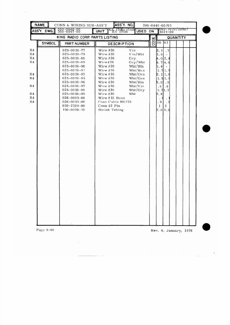
8/9/2019 KX 170A - Maintenance Manual Honeywell
http://slidepdf.com/reader/full/kx-170a-maintenance-manual-honeywell 551/586
SYMBOL
R4
R4
R4
R4
R4
R4
R4
R4
R4
R4
PART NUMBER
025-00 18-77
025-0018-79
025-0018-88
025-0018-89
025-00 18 -90
025-00 18 -9 1
025-00 18 -93
025-0018-95
025-00 18 -96
025-00 18 -97
025-00 18-98
025-0018-99
026-0005-00
026 -00 13 -00
030-2109-00
150-0020-10
DESCRIPTION
Wire #26
Vi0
Wire #26 Vio/Wht
Wire #26
Gry,
Wire #26
Gry/Wht
Wire #26 Wht /Blk
Wire #26
Wht /Brn
Wire #26 Wht /Orn
Wire #26 Wht /Grn
Wire #26 Wht /Blu
Wire #26
WhtlVio
Wire #26
Wht /Gry
Wire #26 Wht
Wire #18 Buss
Coax Cable RG178
Conn 42 Pin
Shrink Tubing
KING RADIO CORl? PARTS LISTING
.
1.
.C
.8
1. ’
.t
.9
1
.E
QUANTITY
1.
1.
1.
.
.8
I
.
=
-
Page 6-66
Rev. 4, January, 1976

8/9/2019 KX 170A - Maintenance Manual Honeywell
http://slidepdf.com/reader/full/kx-170a-maintenance-manual-honeywell 552/586
Parts List Revision Record
Assembly No. 200 -0449-00 /O 1
ACTION SYMBOL
PART NUMBER
DESCRIPTION
QUANTITY
CHANGE
CHANGE
CHANGE
CHANGE
CHANGE
CHANGE
CHANGE
CHANGE
CHANGE
CHANGE
CHANGE
CHANGE
CHANGE
CHANGE
CHANGE
CHANGE
CHANGE
CHANGE
CHANGE
CHANGE
CHANGE
CHANGE
CHANGE
CHANGE
CHANGE
CHANGE
CHANGE
CHANGE
C HANG E
CHANGE
CHANGE
CHANGE
CHANGE
CHANGE
CHANGE
CHANGE
CHANGE
CHANGE
CHANGE
CHANGE
DELETED
DELETED
DELETED
DELETED
ADDED
CHANGE
Rev. 4, January, 1976
025-0003-04
025-0003-12
025-0003-13
025-0003-14
025-0005-02
025-0005-09
025-0018-04
025-0018-14
025-0018-16
025-0018-19
025-0018-22
025-0018-24
025-0018-25
025-0018-26
025-0018-29
025-0018-34
025-0018-36
025-0018-37
025-0018-38
025-0018-39
025-0018-40
025-0018-42
025-0018-43
025-0018-45
025-0018-46
025-0018-47
025-0018-48
025-0018-56
025-0018-57
025-0018-59
025-0018-66
025-0018-77
025-0018-79
025-0018-88
025-0018-89
025-0018-93
025-0018-95
025-0018-97
025-0018-99
026-0013-00
025-0018-00
025-0018-44
025-0018-69
026-0005-00
091-0194-00
025-0018-72
Wire #22 Ye1
1. 3
Wire #22 Red/Wht
.7
Wire #22 Orn/Wht
2. 6
Wire #22 Yel/Wht
1. 9
Wire #18 Red 1. 7
Wire #18 Wht 1. 7
Wire #26 Blk/Yel .9
Wire #26 Brn/Yel
.8
Wire #26 Brn/Blu 1. 4
Wire #26 Brn/Wht 2. 8
Wire #26 Red .9
Wire #26 Red/Ye1 .8
Wire #26 Red/Grn
1. 6
Wire #26 Red/Blu 1. 4
Wire #26 Red/Wht
1. 3
Wire #26 Orn/Yel
.7
Wire #26 Orn/Blu
1. 3
Wire #26 Orn/Vio
1. 3
Wire #26 Orn/Gry 3. 0
Wire #26 Orn/Wht
1. 4
Wire #26 Yel/Blk
1. 4
Wire #26 Yel/Red 1. 0
Wire #26 Yel/Orn
2. 5
Wire #26 Yel/Grn 1. 9
Wire #26 Yel/Blu 1. 3
Wire #26 Yel/Vio 1. 3
Wire #26 Yel/Gry
1. 2
Wire #26 Grn/Blu
1. 4
Wire #26 Grn/Vio
1. 4
Wire #26 Grn/Wht
1. 3
Wire #26 Blu 3. 0
Wire #26 Vio 2. 3
Wire #26 Vio/Wht
1. 3
Wire #26 Gry 4. 4
Wire #26 Gry/Wht 4. 3
Wire #26 Wht/Orn
2. 0
Wire #26 Wht/Grn 1. 6
Wire #26 Wht/Vio .9
Wire #26 Wht
2. 0
Coax Cable RG178
1. 0
Cable Tie
Wire #26 Vio/Red
2. 6
1. 7
1. 7
6
.6
1. 4
.8
1. 6
.8
.6
3. 0
1. 3
1. 8
.7
2. 4
4. 0
1. 6
1. 6
.9
1. 0
28 19
1.3 -
Page 6-67

8/9/2019 KX 170A - Maintenance Manual Honeywell
http://slidepdf.com/reader/full/kx-170a-maintenance-manual-honeywell 553/586
KING,
KY 1958
COMMUNICATIONSRANSCEIVE
INSTALLATIONANUAL
006-0088-01
REV. 1 JANUARY, 1976

8/9/2019 KX 170A - Maintenance Manual Honeywell
http://slidepdf.com/reader/full/kx-170a-maintenance-manual-honeywell 554/586
THIS EQUIPMENT MANUFACTURED UNDER
THE FOLLOWING U. S. PATENT 3,696,422
8/9/2019 KX 170A - Maintenance Manual Honeywell
http://slidepdf.com/reader/full/kx-170a-maintenance-manual-honeywell 555/586

8/9/2019 KX 170A - Maintenance Manual Honeywell
http://slidepdf.com/reader/full/kx-170a-maintenance-manual-honeywell 556/586
KlNG-
KY 195B
COMMUNICATIONS TRANSCEIVER
HISTORYOF REVISIONS
Rev. 1, January,. 1976
Page
Front Page
2-1
2-4A
2-6
2-7
2-9
Reasons for Change
Rev. No. change and Warranty deleted
Paragraph 2.3(b) revised
Antenna Cable Assembly added
Interconnect revised
Added
Added
ii

8/9/2019 KX 170A - Maintenance Manual Honeywell
http://slidepdf.com/reader/full/kx-170a-maintenance-manual-honeywell 557/586
KlNG
KY’195B
COMMUNICATIONS TRANSCEIVER
SECTION
&NERAL NFORMATION
1.1 INTRODUCTION
This manual contains information relative to the physical, mechanical and electrical character-
istics of the King Radio Corporation Silver Crown KY 195B.
1.2 PURPOSEOF EQUIPMENT
The King KY 195B COMM combines in a single panel mounted unit a 720 channel VHF COMM
Transceiver with dual, independent, frequency selectors.
1.3 DESIGNFEATURES
A.
Controls
1. On-Off switch is independent of volume control settings allowing the volume to
remain at desired levels.
2.
Dual control head with thumb switch selection of frequency selector A or
frequency selector B.
3.
Automatic squelch eliminates pilot responsibility for continuously monitoring
squelch adjustments. Squelch threshold automatically adjusts to open on
readable signals.
Test position opens squelch to test COMM receiver sensitivity
and to listen to extremely weak signals.
4.
Frequency selector mechanism features human engineered concentric knobs,
airline type drum readout, and blue-white back
lighting.
B.
Electronics
1.
2.
3.
4.
5.
6.
7.
Varactor diode tuned filters eliminates use of mechanical tuning shafts and
mechanisms.
Balanced mixers for superior intermodulation, cross modulation, and L. 0.
radiation performance.
Transistorized transmitter provides 5 watts minimum output power and long
term reliability superior to tube designs.
The digital frequency synthesizer utilizes state of the art integrated circuits
to replace all but 4 crystals.
Crystal filter selectivity.
Carrier to noise squelch with carrier squelch back up functionally described
above.
Tight AGC (typically 0. 5db from 10~~ to 20,000~~) minimizes audio level
variations.
Page l-l

8/9/2019 KX 170A - Maintenance Manual Honeywell
http://slidepdf.com/reader/full/kx-170a-maintenance-manual-honeywell 558/586
KlNG
KY 195B
COMMUNICATIONS TRANSCEIVER
C.
Construction
1.
Modular construction for ease of maintenance.
2. Rack mounted, removable from the front panel.
3.
Anti-theft locking mechanism available.
1.4 POWERREQUIREMENTS
The KY 195B requires 13.75 volts for proper operation.
Aircraft having electrical power plants
producing 27.5 volts require the installation of a voltage converter. The KA 39 Voltage
Converter, designed to convert 27.5 volts to 13. 75 volts,
may be conveniently remote mounted
in the aircraft.
1.5 TECHNICAL HARACTERISTICS
CDTJ,-‘TTZ’TP A ‘PTT\T,l
~~ T
PUAR ACTF’RTSTTC
UI YVIK LULL I I”J.1
TSO COMPLIANCE:
COMM Thansmit
COMM Receive
Environmental
MOUNTING :
SIZE :
V~~L..A.“LIV A LILUIVA AV
I
1 KY 195B TRANSCEIVER(
1
C37b (00-110, Class II)
C38b (00-109)
DAPBAAXXXXXX
Panel mounted, no shock mounting required
6.3 12 X 2.600 X 14. 15 inches w/connectors.
(16.03 X 6.60 X 35.94 centimeters)
WEIGHT :
POWER REQUIREMENTS:
COMM Receive
COMM Transmit (Tone)
Lamps
6.0 lbs. excluding external connectors and
harness. (2. 7Kg)
13.75V (or 27. 5V with KA 39)
0.70 amps
4. 5 amps (2.8 amps unmodulated)
0: 16 amps (13.75Vdc1, 0.08 amps (27. 5Vdc)
CRYSTAL CONTROLLED:
720 channels
FREQUENCY RANGE:
118.000 to 135.975lVIHz with 25kHz spacing
FREQUENCY STABILITY:
io. 003%
VHF POWER OUTPUT:
5 watts minimum, 50 ohm load
Page l-2

8/9/2019 KX 170A - Maintenance Manual Honeywell
http://slidepdf.com/reader/full/kx-170a-maintenance-manual-honeywell 559/586
KlNG
KY 195B
COMMUNICATIONS TRANSCEIVER
SPECIFICATION
MODULATION:
MICROPHONE:
CHARACTERISTIC
85% modulation capability with 90% limiting,
less than 15% distortion at 80% mod.
Carbon or dynamic mike containing transistor-
ized pre-amp (must provide at least 120mvrmr
into 500R load).
SIDETONE:
DUTY CYCLE:
SENSITIVITY:
SELECTIVITY:
SPURIOUS RESPONSES:
SQUELCH:
AGC CHARACTERISTICS:
AUXILIARY AUDIO INPUTS:
Adjustable up to 4mw into 500 ohm headphones
1 minute on, 4 minutes off (20%)
(RECEIVER]
1. 5pv (soft) will provide a 6db minimum
signal plus noise to noise ratio
Typical 6db at f8kHz, 70db at *25kHz
Down at least 60db
Automatic squelch (carrier to noise) with
manual disable and carrier squelch override.
From 10~~ to 20,000~~ audio output will not
vary more than 3db.
[AUDIO [
Two (2) 500 ohms with 30db isolation between
any two.
INTERCOM INPUTS:
FREQUENCY RESPONSES:
HEADPHONE OUTPUT:
SPEAKER OUTPUT:
One (1) Intercom Microphone Input. (Micro-
phone must provide at least 120mvrms into
5OOa load).
Within 6db from 350Hz to 2500Hz.
50mw into 500 ohm
4.5Vrms into auxiliary input produes 5 watts
audio output
SIZE :
3.500 X 2.000 X 5. 500 inches
(8.89 X 5.08 X 13. 97 centimeters)
WEIGHT :
1. 1 lbs. (. 5Kg) excluding harness
Page 1-3

8/9/2019 KX 170A - Maintenance Manual Honeywell
http://slidepdf.com/reader/full/kx-170a-maintenance-manual-honeywell 560/586
KING
KY 195B
COMMUNICATIONS TRANSCEIVER
SP??C:IATION
POWER:
Input Volts
output Volts
CHARACTERISTIC
A B
’ 27. 5vdc 27. 5vdc
13. 75vdc
13.75vdc
(nominal) (nominal)
I
Output Current continuous
i. 5A
0.75A
Output Current 40% duty 5.OA
------------
I
1.6 UNITS AND ACCESSORIESUPPLIED
A.
King KY 195B COMM (069-1021-00)
B.
King KY 195B Installation Kit (050-1142-02) includes the following parts:
030-0061-00
030 - 10 19 -00
030 -2 10 l-04
047-1851-00
088-0136-01
089-2 188 -22
089-5523 -05
089-5903-05
089-5907-05
089 -6008 -04
089-8025-30
089-8094-30
090-0019-07
047 - 1743 -0 1
Connector, Antenna (TED 9 - 10 -2)
Clamp, Cable Hall
Connector, 42 pin (Amphenol 26-190-42)
Cover, Connector Mounting Plate
Filter, Red Lamp
E4 ESNA Nut
Screw, #4-40 X 5/16 F il HP
Screw, #4-40 X 5/16 PHP
Screw, #6-32 X 5/16 PHP
Screw, #4-40 X l/4 FHP
Flat Washer
Flat Washer
Ring, Retainer
Plate, Connector Mounting
1.7 ACCESSORIESEQUIRED, UT NOTSUPPLIED
A.
Communication antenna and cables
B.
Headphones and speaker:
1.
Headphones: Low impedance types, 300 to 1,000 ohms.
2.
Speaker: Voice coil impedance 3 to 6 ohms nominal.
1
2
1
1
2
2
4
2
2
4
2
2
2
1
C.
KA 39 Voltage Converter, 27. 5V to 13. 75V (required in 27. 5V installation only).
D. Microphone: Low impedance carbon, or dynamic with transistor preamp, such as
King IL4 14.
Page l-4

8/9/2019 KX 170A - Maintenance Manual Honeywell
http://slidepdf.com/reader/full/kx-170a-maintenance-manual-honeywell 561/586
KlNG
KY 195B
COMMUNICATIONS TRANSCEIVER
1.8 LICENSEREQUIREMENTS
The Federal Communications Commiss ion requires that the operator of the transmitter of this
equipment hold a Restricted Radio Telephone Operator Permit, or higher class license.
A
permit may be obtained by an U. S. citizen from the nearest field office of the FCC; no exami-
nation is required.
This equipment has been type accepted by the FCC and entered on their list of type accepted
equipments as King KY 195B and must be identified as King KY 195B.
-CAUTION -
The VHF transmitter in this equipment is
guaranteed to meet Federal Communications
Commission approval only when King crystals
are used.
Use of other than King crystals is considered
an unauthorized modification.
Page l-5
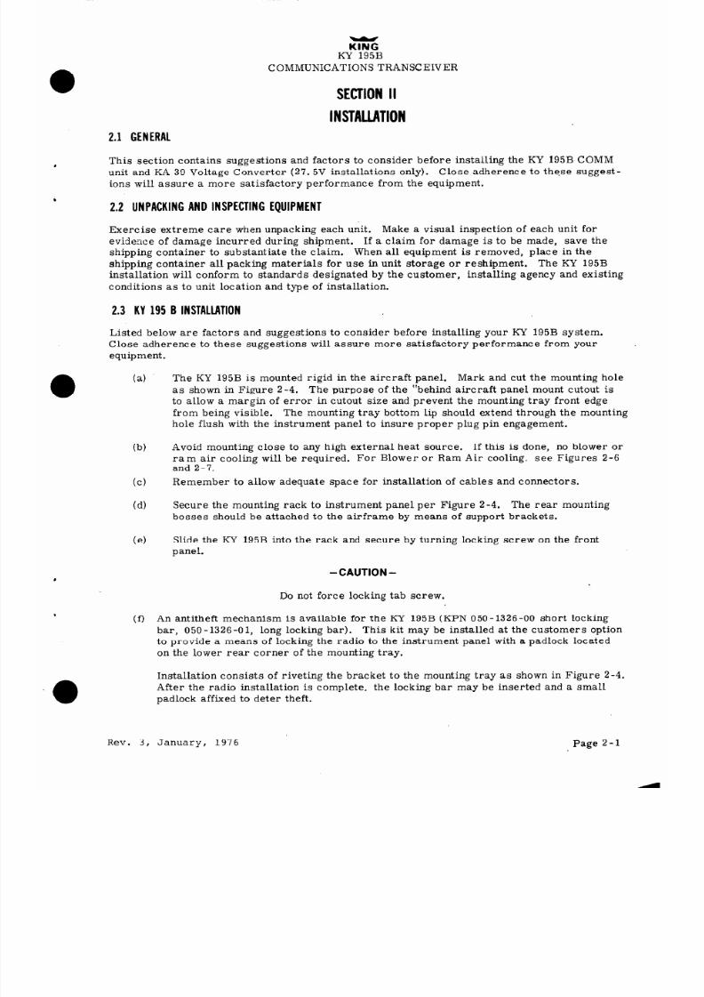
8/9/2019 KX 170A - Maintenance Manual Honeywell
http://slidepdf.com/reader/full/kx-170a-maintenance-manual-honeywell 562/586
KlNG
KY 195B
COMMUNICATIONS TRANSCEIVER
SECTIONI
INSTALLATION
2.1 GENERAL
This section contains suggestions and factors to consider before installing the KY 195B COMM
unit and KA 39 Voltage Converter (27. 5V installations only).
Close adherence to these suggest-
ions will assure a more satisfactory performance from the equipment.
2.2 UNPACKING ND INSPECTING QUIPMENT
Exercise extreme care when unpacking each unit.
Make a visual inspection of each unit for
evidence of damage incurred during shipment. If a claim for damage is to be made, save the
shipping container to substantiate the claim.
When all equipment is removed, place in the
shipping container all packing materials for use in unit storage or reshipment.
The KY 195B
installation will conform to standards designated by the customer,
installing agency and existing
conditions as to unit location and type of installation.
2.3 KY 195 B INSTALLATION
Listed below are factors and suggestions to consider before installing your KY 195B system.
Close adherence to these suggestions will assure more satisfadtory performance from your
equipment.
(a)
(b)
(c)
(4
(4
(f)
The KY 195B is mounted rigid in the aircraft panel.
Mark and cut the mounting hole
as shown in Figure 2-4. The purpose of the “behind aircraft panel mount cutout is
to allow a margin of error in cutout size and prevent the mounting tray front edge
from being visible.
The mounting tray bottom lip should extend through the mounting
hole flush with the instrument panel to insure proper plug pin engagement.
Avoid mounting close to any high external heat source.
If this is done, no blower or
ram air cooling will be required.
For Blower or Ram Air cooling. see Figures 2-6
and 2-7.
Remember to allow adequate space for installation of cables and connectors.
Secure the mounting rack to instrument panel per Figure 2-4.
The rear mounting
bosses should be attached to the airframe by means o f support brackets.
Slide the KY 195B into the rack and secure by turning locking screw on the front
panel.
-CAUTlON-
Do not force locking tab screw.
An antitheft mechanism is available for the KY 195B (KPN 050 - 1326 -00 short locking
bar, 050-1326-01, long locking bar). This kit may be installed at the customers option
to provide a means of locking the radio to the instrument panel with a padlock located
on the lower rear corner of the mounting tray.
Installation consists of riveting the bracket to the mounting tray as shown in Figure 2-4.
After the radio installation is complete, the locking bar may be inserted and a small
padlock affixed to deter theft.
Rev. 3, January, 1976
Page 2-l

8/9/2019 KX 170A - Maintenance Manual Honeywell
http://slidepdf.com/reader/full/kx-170a-maintenance-manual-honeywell 563/586
KlNG
KY 195B
COMMUNICATIONS TRANSCEIVER
2.4 KA 39 ‘INSTALLATION
(For use in 27. 5 volt installations only)
(a)
Select the KA 39 location considering good thermal conductivity to the air-
frame, convenient cable routing, proximity to the KY 195B and separation
from other heat sources.
lb)
Refer to Figure 2-3 for the KA 39 mounting dimensions
(4
Secure the KA 39 firmly in place
(d)
The installing agency will supply and fabricate external cables
2.5 ANTENNANSTALLATION
(a)
A conventional 50 ohm vertically polarized COMM antenna is required with
the KY 195B. Vertical bent whip antennas are not recommended
Wideband
COMM antennas provide efficient operation over the COMM band Antennas
should be installed per manufacturers recommendations. Additional rec-
ommendations are as follows
1. Mount antenna on flat metal surface or install a ground plane at least
18 inches square.
2.
The antenna should be well removed from any projections including the
engine(s) and propeller.
3.
The COMM Antenna should be well separated from any NAV Antenna to
minimize COMM interference to NAV while transmitting (30db min. ).
(b)
Refer to Figure 2-2 for the COMM antenna cable connector assembly.
Solder tack the snap on shield to the connector base at two points to insure
that a good electrical ground is made.
2.6 CABLING
(a)
The length and routing of the external cables must be carefully studied and
planned prior to installation. Avoid sharp bends and placing cables too
near the aircraft control cables.
b)
Fabricate the external cables in accordance with the installation drawing
that fulfills the system requirement.
-NOTE-
Use good quality stranded wire that will not support
a flame and with at least 600 volts insulation.
It is
recommended that the mike audio line be in a shield-
ed-twisted pair.
(4
Since other radio equipment will possibly utilize the same speaker circuits
for muting, speaker selection and microphone switching must be devised
by the installing agency.
Page 2-2

8/9/2019 KX 170A - Maintenance Manual Honeywell
http://slidepdf.com/reader/full/kx-170a-maintenance-manual-honeywell 564/586
KlNG
KY 195B
COMMUNICATIONS TRANSCEIVER
16.: $7. ,111 e
PI71
I
CONNECTOR YIEWED
KPN 030-2101-04
FAOM C&&E END
FIGURE 2-1 KY 195B CONNECTOR PIN LOCATIONS
(DWG. NO. 696-6002-00 R-O)
/-SOLDER
Trim coax cable outer insulation as shown.
Fold braid back over outer cover of coax.
Do not cross strands.
Solder center conductor to center pin of
conductor. Make sure front end of braid
(Point of fold) is even with bottom of connector.
(Shown by arrows)
Slide connector cap,
with clearance hole in
position to clear dielectric, on to connector
until it snaps in place.
Push braid forward and flatten against con-
nector cap and solder.
Solder tat connector cap to connector in at
least twy places to insure good electrical
contact.
FIGURE 2-2 ANTENNA CABLE ASSEMBLY
(DWG. NO. 696-6005-00 R-O)
Page 2-3

8/9/2019 KX 170A - Maintenance Manual Honeywell
http://slidepdf.com/reader/full/kx-170a-maintenance-manual-honeywell 565/586
,KING
KY 195B
COMMUNICATIONS TRANSCEIVER
.093R 2 PLCS.
USE’S PAN HO. SCREWS
I-
5.500
(13.870)
-I
155-5076-00 (R- )
NOTES:
I. ALL DIMENSIONS IN PARENTHESIS ARE IN CENTIMETERS.
ZWEIGHT: 1.1 Ibe
3 TERMINALS WILL TAKE 16TOZZAW G WIRE.
4TERMlNALS ARE ff5-40YIA ED. HO. SCREWS.
WARNING
-
DONOT MOUNT IN CLOSE PROXIM ITY
TO HEATER DUCT OR OTHER SOVRCES OF HEAT
I
FIGURE 2-3 KA 39 VOLTAGE CONVERTER OUTLINE AND MOUNTING DRAWING
(DWG. NO. 155-5076-00 R-O)
Page 2-4
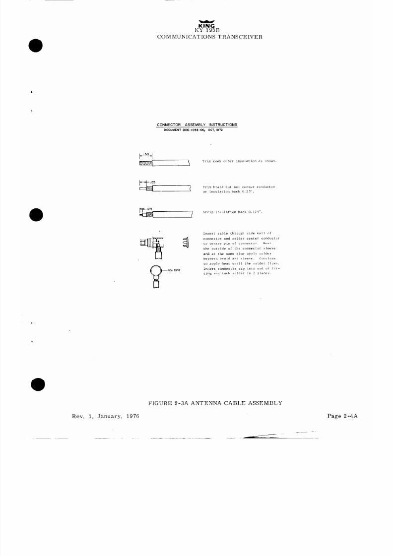
8/9/2019 KX 170A - Maintenance Manual Honeywell
http://slidepdf.com/reader/full/kx-170a-maintenance-manual-honeywell 566/586
KlNG
KY 195B
COMMUNICATIONS TRANSCEIVER
CONNECTOR ASSEMBLY INSTRUCTIONS
DOCUMENT 006-1058-00. OCT, 1972
I
Trim braid but not center conductor
or insulation back 0.25”.
Strip insulation back 0.125”
Insert cable through side ~11 of
connector and solder center conductor
to center pin of connector. Heat
the ‘outside of the connecror sleeve
and at the same tine apply solder
between braid and sleeve.
Cant inue
to apply heat until the solde r flow\.
Insert connector cap into end oi fit-
ting and tack solder in 2 places.
FIGURE 2-3A ANTENNA CABLE ASSEMBLY
Rev. 1, January, 1976
Page 2-4A

8/9/2019 KX 170A - Maintenance Manual Honeywell
http://slidepdf.com/reader/full/kx-170a-maintenance-manual-honeywell 567/586
L.
-
-4
f
P
0
0
-
FIGURE 2-4 KY 195B OUTLINE AND MOUNTING ~R.AWING
(DWG. NO. 155-5108-00 R-O)
Page 2-5

8/9/2019 KX 170A - Maintenance Manual Honeywell
http://slidepdf.com/reader/full/kx-170a-maintenance-manual-honeywell 568/586
KING
KY 195B
COMMUNICATIONS TRANSCEIVER
7
K
Y
i
/
t:
I
3
B
030-2101-04
P171
-
33
38
20
-2
17
16
41
- IMT LIGHT DI dXER ~ 13.75VDC DIMMER CONTROL
-INST LIGHT DIMMER -A
-A/C POWER-#16Ah'G---
5A
-A/C POWER 13.75VDC
-SPARE
-COMM SWITCHED A/C POWER--16AWG
-COMM 13.75VDC INPUT
-SPEAKER OUTPUT-
21
39
40
36
37
15
16
3i
35
3
4
6
7
8
9
10
1L
12
13
14
1
19
2
5
22
23
24
25
27
28
29
30
31
32
26
-
f
SPFAKER RETURN-
POWER GROUND y("16AWG)
Y
7 MIKE AUDIO
&MIKE KEY
-AUX AUDIO il
-AU4 AUDIO $2 (NOTE 7)
-AUX AUDIO #3
-AUX AUDIO #II
--corni 5OOM OUTPUT
030.0061:OO OK 030-010t-00
P172
RGSBAIU-TO corn ANT.
NOTES:
1.
UNLESS NOTED, ALL W IRES TO BE #24AWG MINIMUM.
2.
IF SPEAKER IS NOT USED. INSTALL A 4s. low RESISTOR TO SIMULATE LOUD
BETWEEN FINS 41 AND 21.
3. ALL GROUNDS ARE AIRFRAME GROUNDS UNLESS OTHERWISE NOTED.
6.
27.5VDC OPERATION:
KY195 KYL95B.
P/O PL71
INST LIGHT DIFDlER-NC
INST LIGHT DIMMER-27.5VDC DIMMER CONTROL
A/C FOWER--P16AWG-~-27.5VDC A/C POWER
COtm SWITCHED A/C ROWE R-#L6AWG
OllTPII'I INPLlT
COMM 13.75VDC INPUT-#16Ah'G
(1.5A CONTINUOUS)
(5.OA 20'. DUTY FACTOR)
jF* qc
= R
5.
POWER BUSS CIRCUIT BREAKERS ARE TO BE MOUNTED IN THE AIRCRAFT BREAKER
PANEL OR INSTRUMENT PANEL SUCH THAT THEY WILL BE ACCESSIBLE IN FLIGHT
AND SAFE FROM PHYSICAL DAMAGE.
6. THE KY195 WIL L FUNCTION PROPERLY WHEN PLUGGED INTO KXl75 OR KX170A
INSTALLATIONS. REFER TO KX170AlKX175 INSTALLATION MANUAL (006-0057-00).
7.
AUXILIARY AUDIO d2 IS INTERCOM MIC.INPUT ON KY195B. KX170B/KEL75B ONLY.
8.
THE KYL95B WILL FUNCTION PROPERLY WHEN PLUGGED INTO KXl70B OR KX175B
INSTALLATIONS.
REFER TO KX170B/KXl758 INSTALLATION PWSUAL (006.CG::-00).
ONE POSSIBLE INTERCONNECT IS SHOlrN BELOW.
I
PCT
L
PILOT TX
INTERC. .
‘0
COPILOT TX.
FIGURE 2-5 KY 195 INTERCONNECT
(DWG. NO. 155-1099-00 R-3)
- PILOT MIKE
Pl71
030-2101-04
39 TX MIKE AUDIO
37 INTER COM MIKE
AUDIO
-COPILOT MIKE
\
0
0
-=-.-P_ 2 -5 __-_- Rev. 1,’ January, 1976
- ----\
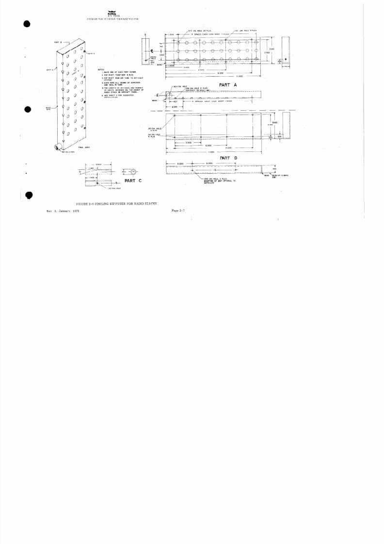
8/9/2019 KX 170A - Maintenance Manual Honeywell
http://slidepdf.com/reader/full/kx-170a-maintenance-manual-honeywell 569/586
KB
COMMUNICATIONS TRANSCEIX’ER
,.375 DIA. HOLE 30 PLCS.
/I30 DIA. HOLE 4 PLCS
4
p- 1. 500
9 SPACES EACH 1.000 APART = 9 000
NOTE 2
t -I
750
‘USER
NOTES:
I . M AK E O NE
2. POP RIVET
3. POP RIVET
HOUSNG
OF EACH PART SHOWN
TOGETHER 6 PLCS.
RAM AIR TUBE TO DIFF
4. DUCK TAPE ALL SEAMS OF DIFFUSER
AND SEAL IN TUBE
5 . T HE L EN GT H O F D IF FU SE R. A ND N UM BE R
O F H OL ES . O EP EN DS O N T HE H EI GH T O F
RADIO STACK OR AIRCRAFT PANEL
PART A
9 SPACES EACH 1.000 APART =9.000
6. SEE SHEET 2 FOR SUGGESTED
INSTALLATION.
,130 DIA. HOL
4 PLCS
,126 DIA. H
4 PLCS
‘NOTES 3 Et4
b- 11.000
I
R4RT B
3.000 5.000 I
____--_-----
_--- -----
--
t
c +
.750
_____ -- ------~~
__----- ----
1---------
- k EN D - bE ND U P T O M AK E
END
,093 D IA. HOLE 2 PLCS
M OU NT N G O F U N T O PT IO NA L T O
INSTALLER.
I
4
.62 5 -+-
0
PART C
.I26 DIA. HOLE
FIGURE 2-6 COOLING DIFFUSER FOR RADIO STACKS
Rev 1, January, 1976
Page 2-7

8/9/2019 KX 170A - Maintenance Manual Honeywell
http://slidepdf.com/reader/full/kx-170a-maintenance-manual-honeywell 570/586
KY 195B
COMMUNICATIONS TRANSCEIVER
, P ANE L
KT 76 /78
KX 1758
KX 1758
L DU CT . T UB IN G TO
KAIB’RAM AIR KIT
(150-0083-00)
TYPICAL INSTALLATION
KA 16-KPN(071-4001-00) AND DIFFUSER STACK
FIGURE 2-7 KR 16 RAM AIR KIT AND DIFFUSER INSTALLATION
Rev 1, January, 1976 Page 2-9
BEND TABS OVER MANIFOLD
WHEN MANIFOLD IS POSITIONEN AS
( -R EQD . )
VIEW B
KUiJ
LWATE, PROOF UNT IN THIS AREA ’
INCLUDING ENDS OF MOUNTNG SCREWS
WITH A ZINC CHROMATE SEALER,OR
EQUIVALENT.
( U N Tv w S~ ~W N T UR NE D 1 60 ° F RO M
HOLE
i

8/9/2019 KX 170A - Maintenance Manual Honeywell
http://slidepdf.com/reader/full/kx-170a-maintenance-manual-honeywell 571/586
KING.
KY 195B
COMMUNICATIONSTRANSCEIVER
SECTIONII
OPERATION
3.1 GENERAL
All controls required ‘to operate the KY 195B are located on the unit front panel.
3.2 KY 195B COMM CONTROLS
3.2. 1
COMM ON-OFF TEST CONTROL
The ON-OFF-TEST control is located directly above the COMM A channel selector. Power is
supplied to the COMM when this control is either in the ON or TEST position.
The TEST position
is used to defeat the COMM automatic squelch for both test purposes and listening to extremely
weak signals.
3.2.2 COMM VOLUME CONTROL
The Volume (VOL) control, located on the lower left side of the KY 195B is used to adjust the
transceiver audio volume.
The KY 195B system power ON/OFF switch is independent of this
control, allowing the COMM volume to remain at a desired preset level.
3.2.3
COMMA FREQUENCY SELECTOR
The two concentric knobs under the COMM A frequency window are used to dial COMM A
frequencies. The larger knob selects MHz and the smaller knob selects KHz. The transceiver
is inoperable in the two unused MHz positions between 118MHz and 135MHz. Clockwise rotation
selects higher frequencies. The dial mechanism has no stops, permitting continuous rotation.
3.2. 4.
COMM B FREQUENCY SELECTOR
The two concentric knobs under the COMM B frequency window are used to dial COMM B
frequencies. The larger knob selects MHz and the smaller knob selects KHz. The transceiver
is inoperable in the two unused MHz positions between 118MHz and 135MHz. Clockwise rotation
selects higher frequencies.
The dial mechanism has no stops, permitting continuous rotation.
3.2. 5 A-B SELECTOR CONTROL
The A-B leverswitch is used to select control head A or control head B.
Page 3-l

8/9/2019 KX 170A - Maintenance Manual Honeywell
http://slidepdf.com/reader/full/kx-170a-maintenance-manual-honeywell 572/586
KING
KY 195B
COMMUNICATIONS TRANSCEIVER
COMM A FREQUENCY REAOOUT
MHz FREQUENCY SELECTOR A
MHz FREQUEPdCYSELECTOR
KHz FREOUENCY SELECTOR A
KHz FREQUENCY SELECTOR B
VOLUME CONTROL
ON-OFF-TEST SWITCH
A-B SELECTOR CONTROL
FIGURE 3-l KY 195B CONTROL FUNCTIONS
3.3 POST-INSTALLATIONHECKOUT
An operational performance flight test is recommended after the installation is completed to
insure satisfactory performance of the equipment in its normal environment.
To check the communications transceiver,
maintain an appropriate altitude and contact a ground
station facility at a range of at least fifty nautical miles.
Contact a ground station close in.
Place the squelch knob in the test position and listen for any unusual electrical noise which would
reduce the COMM receiver sensitivity by increasing the squelch threshold. If possible, verify
the communications capability on both the HIGH and LOW ends of the VHF COMM band.

8/9/2019 KX 170A - Maintenance Manual Honeywell
http://slidepdf.com/reader/full/kx-170a-maintenance-manual-honeywell 573/586
MAINTENANCE/OVERHAUL
MANUAL
KY 195B
COMMUNICATIONS
TRANSCEIVER
KING RADIO CORPORATION,
400 NORTH ROGERS ROAD
OLATHE, KANSAS, U.S.A.

8/9/2019 KX 170A - Maintenance Manual Honeywell
http://slidepdf.com/reader/full/kx-170a-maintenance-manual-honeywell 574/586
KlNG
KY 195B
COMMUNICATIONS TRANSCEIVER
TABLE FCONTENTS
SECTIONV THEORYFOPERATIONNDMAINTENANCE
Paragraph Page
4. 1
4.2
4.3
4.3. 1
4.3.2
4.4
Item
1. KY 195B
5-1
2.
Front Plate Sub-Assembly
5-l
3.
Switching Head Sub-Assembly
5-l
4.
COMM SMO Board Sub-Assembly
5-l
5.
COMM SMO Sub-Assembly
5-l
6.
NAV /COMM Board Sub-Assembly
5-l
7.
Transmitter Board Sub-Assembly
5-l
8.
Rear Plate Sub-Assembly
5-l
9.
Audio Drive Board Sub-Assembly
5-l
10.
Rear Divider Sub-Assembly
5-l
11. Connector & Cable Sub-Assembly 5-l
12.
KA 39 Voltage Converter
5-l
13.
Switching Matrix Sub-Assembly
5-2
Figure
5-l Switching Matrix Sub-Assembly
General
Dual Control Head
Dual Control Head-Detailed Description
Control Head Selector in “A” Position
Control Head Selector in “B” Position
Troubleshooting the Dual Control Head
SECTION ILLUSTRATEDARTS IST
4-l
4-l
4-l
4-l
4-l
4-l
LISTOF LLUSTRATIONS
5-5

8/9/2019 KX 170A - Maintenance Manual Honeywell
http://slidepdf.com/reader/full/kx-170a-maintenance-manual-honeywell 575/586
KING
KY 195B
COMMUNICATIONS TRANSCEIVER
SECTIONV
THEORY FOPERATION/MAINTENANCE
4.1 GENERAL
KY 195 unit incorporates a 720 channel communications transceiver, a 5 watt audio system, and
dual control heads.
The transceiver and audio systems are identical to the respective portions of
the KX 175B. For theory and maintenance procedures on the COMM transceiver or audio system,
refer to the KX 175B text.
Theory and maintenance of the dual control head mechanism appear in
this section.
4.2 DUALCONTROL EAD
Wafe r switches in the KY 195B are identical to the COMM wafer switches used in the KX 175B.
Lever switch “A-B” applies either
“A” or “B” channeling information to the SMO and “A” o r “B”
tuning voltage to the varactor tuned filters in the COMM receiver preselector.
4.3 DUALCONTROLEAD-DETAILEDESCRIPTION
Refer to Figure 5-31 in the KX 170B/KX 175B Maintenance Manual for the KY 195B Switching
Assembly Diagram.
4. 3. 1
Control Head Selector in “A” Position
The DPST switch (Sill) contacts are open and the “B” tuning voltage (red-blue wire) from switch
wafer S106 is disconnected from the COMM tuning voltage buss,
Additionally, the common wire
to the “B” switch wafers (red-gray wire) assumes a voltage of approximately 8 volts, back bias-
ing the isolation diodes associated with the “B” wafer switches which effectively disconnects the
“B” switching circuitry from the COMM SMO.
Transistors Q201-Q204 are saturated. Q204
shorts the common wire of the “A” switch wafers (brown-gray wire) to ground, activating the
“A” wafer switch functions. Q203 connects the negative side of the “A” tuning voltage divider on
switch wafer, S102, to ground while Q201 connects the positive side to +8. 5VDC providing a
current path through the tuning voltage divider. The “A” tuning voltage from switch wafer S102 is
connected directly to the COMM tuning voltage buss (red-blue wire) providing “A” tuning voltage
to the COMM receiver preselector.
4. 3. 2
Control Head Selector in “B” Position
The DPST switch (Sill) contacts are closed, connecting (a) the COMM tuning voltage from switch
wafer S106 to the tuning voltage buss (red-blue wire) and (b) the common wire of the “B” switch
wafers (red-gray wire) to ground. With the common wire on ground, the “B” channeling wafers
are activated and transistors Q201-Q204 are off. With Q203 and Q201 off, no current flows
through the “A” tuning voltage divider on switch wafer S102, isolating it from the COMM tuning
voltage buss (red-blue wire).
With Q204 off, the “A” wafers and associated isolation diodes
represent an open circuit to the COMM SMO frequency selection circuitry.
4.4 TRDUBLESHDDTINGHE DUALCONTROL EAD
Refer to Figure 5-3 1 in the KX 170B/KX 175B Maintenance Manual for the KY 195B switching
matrix voltage measurements.
See the KX 175B Manual for channeling malfunctions, refer to
Table 4-3 “COMM Programmable Counter Coding”
and for COMM receiver preselector tuning
voltage versus channel frequency see Table 5-3 “COMM Channel-Receive SMO Frequency-Tuning
Voltage, ”
February, 1973
Page 4-1
8/9/2019 KX 170A - Maintenance Manual Honeywell
http://slidepdf.com/reader/full/kx-170a-maintenance-manual-honeywell 576/586
KlNG
KY 195B
COMMUNICATIONS TRANSCEIVER
1.
KY 195B-See page 6-l and 6-2 in Kx 170B/KX 175B Maintenance Manual.
2.
FRONT PLATE SUB-ASSEMBLY-See pages 6-4 thru 6-9 in KX 170B/KX 175B Maintenance
Manual.
3. SWITCHING HEAD SUB-ASSEMBLY-See pages 6-10 thru 6-14 in KX 170B/KX 175B
Maintenance Manual.
4.
COMM SMO BOARD SUB-ASSEMBLY-See pages 6-32 thru 6-38. For schematic and
assembly drawing see page 5-69 of the Kx 170B/
KX 175B Maintenance Manual.
5.
COMM SMO SUB-ASSEMBLY-See pages 6-39 thru 6-41 in KX 170B/KX 175B Maintenance
Manual.
6. NAV/COMM BOARD SUB-ASSEMBLY-See pages 6-42 thru 6-50 in Kx 170B/KX 175B
Maintenance Manual.
For schematic and assembly
drawings see pages 5-63 and 5-63A in KX 170B/
KX 175B Maintenance Manual.
7. TRANSMITTER BOARD SUB-ASSEMBLY-See pages 6-51 thru 6-53 in Kx 170B/KX 175B
Maintenance Manual. For schematic and
assembly drawing see page 5-67 in KX 170B/
KX 175B Maintenance Manual.
8.
REAR PLATE SUB-ASSEMBLY-See pages 6-54 thru 6-56 in Kx 170B/KX 175B Maintenance
Manual. For assembly drawing see page 6-60 in Kx 170A/
KX 175 Maintenance Manual.
9. AUDIO DRIVE BOARD SUB-ASSEMBLY-See pages 6-57 thru 6-59 in KX 170B/KX 175B
Maintenance Manual. For schematic and assembly
drawing see page 5-67 in Kx 170B/KX 175B
Maintenance Manual.
10.
REAR DIVIDER SUB-ASSEMBLY-See pages 6-60 thru 6-63 in m 170B/KX 175B
Maintenance Manual.
11.
CONNECTOR & CABLE SUB-ASSEMBLY-See pages 6-65 thru 6-67 in KX 170B/KX 175B
Maintenance Manual.
12.
KA 39 VOLTAGE CONVERTER-See pages 6-71 thru 6-74 in KX 170A/KX 175 Maintenance
Manual.
February, 1973
Page 5-l

8/9/2019 KX 170A - Maintenance Manual Honeywell
http://slidepdf.com/reader/full/kx-170a-maintenance-manual-honeywell 577/586
KING RADIO CORf? PARTS LISTING
=
=
SYMBOL
PART NUMBER
DESCRIPTION
009-0030-02 T ertiinal St rip
012-1006-00 Nyl Lacing Tape
025-0018-04
#26 Wire
Blk/ Ye1
025-0018-14 #26 Wire Brn/ Ye1
025-0018-24 #26 Wire
Red/ Ye1
025-0018-34 #26 Wire Orn/ Ye1
025-0018-44 #26 Wire Ye1
025-0018-54 #26 Wire Grn/Yel
025-0018-56 #26 Wire Grn/Blu
025-0018-64 #26 Wire Blu/Yel
025-0018-74 #26 Wire
Viol Ye1
025-0018-84 #26 Wire Gry/Yel
026-0001-00 #26 Buss Wire
047-2362-02
Chassis SW Matrix
076-0339-00 Spacer
089-2076-30 Nut 4-40
089-5878-05 Scr 4-40 x 5116 PHP
089-8003-34 Washer S/L
150-0003-10 Tubing Tef #24 AWG
Q201
007-0238-00
Tstr FPN4917
Q202
007’-0078-00 Tstr 2N3415
Q203
007-0078-00 Tstr 2N3415
Q204
007-0078-00 Tstr 2N3415
CR201
007-6033-00
Diode lN270
CR202
007-6033-00 Diode lN270
CR.203
007-6033-00
Diode 11\T2 73
CR.204
007-6033-00 Diode lN270
CR205
007-6033-00
Diode lN270
CR206
007-6033-00 Diode lN270
CR207
:007-6033-00 Diode lN270
CR208
007-6033-00 Diode lN270
CR.209
007-6033-00 Diode lN270
CR210
007-6033-00 Diode lN270
CR.211
007-6033-00
Diode lN270
CR212 007-6033-00 Diode lN270
CR213
007-6033-00 Diode lN270
CR214
007-6033-00
Diode lN270
CR215
007-6033-00 Diode lN2 70
CR216
007-6033-00 Diode lN2 70
CR217
007-6033-00 Diode lN270
CR218
007-6033-00 Diode lN270
CR219
007-6033-00 Diode lN270
CR220
007-6033-00
Diode lN270
c
=
00
5
AF
.3
.3
.3
.3
.5
.5
1. (
.4
.4
.4
.2
1
1
5
1
5
.2
1
1
1
1
1
1
1
1
1
1
1
1
1
1
1
1
1
1
1
1
1
1
1
1
-
QUANTITY
069-1021-00
-
-
Page 5-2 February, 1973

8/9/2019 KX 170A - Maintenance Manual Honeywell
http://slidepdf.com/reader/full/kx-170a-maintenance-manual-honeywell 578/586

8/9/2019 KX 170A - Maintenance Manual Honeywell
http://slidepdf.com/reader/full/kx-170a-maintenance-manual-honeywell 579/586
Parts List Revision Record
Assembly No: 200-0459-00
Manual Revision 0
ACTION
SYMBOL
PART NUMBER
DESCRIPTION .,
QUANT IT Y
.
Page 5-4
February, i973

8/9/2019 KX 170A - Maintenance Manual Honeywell
http://slidepdf.com/reader/full/kx-170a-maintenance-manual-honeywell 580/586
INGTH
TO
300-0656-00 P306
P302
P305
P304
P303
P306
P307
P309
P310
300--0656-00 P301
COLOR
GRN /BLU
ORN/YEL
REDIYEL
BRN/YEL
BLK/YEL
GRY/YEL
VIO/YEL
BLU/YEL
GRN/YEL
YEL
UNLESS NOTED. ALL WlRE 025-0016-xX
REF. B/M 200-04 59-00
KlNG
KY 195B
COMMUNICATIONS TRANSCEIVER
026-0001-00~
150-0003-10
047-23x-02-
076-0339-00
089.5878-05c
(SCREW FARSIDEI
FUNCTION
012-1006.WC
0
0202 Cl204 0
0
-009-0030-02 (5)
089-2076-30(51
~089-6003-34~51
0
FIGURE 5-l SWITCHING MATRIX SUB-ASS’Y
(Dwg, No. 300-0662-00) R-l
February, 1973
Page 5-5
8/9/2019 KX 170A - Maintenance Manual Honeywell
http://slidepdf.com/reader/full/kx-170a-maintenance-manual-honeywell 581/586
KlNG
Kx 170BE
NAVIGATION RECEIVER
COMMUNICATION TRANSCEIVER
KX 170BE
1. 1 This section contains information relative to the King Radio Corporation KX 170BE
Communications Transceiver/Navigation Receiver.
The KX 170BE is identical to the
KX 170B with the exception of the Communication Transceiver Selectivity.
Refer to the KX 170B text and the changes listed below to completely specify the KX 170BE.
1. 2 Page 1-3,
Section 1. 5 Technical Characteristics should read:
SPECIFICATION CHARACTERISTIC
RECEIVER SELECTIVITY
Typical 6db at +15KHz
65db at +50KHz
I
1. 3 Page 1-9,
Section 1. 6 Units and Accessories Supplied should read:
A.
King KX 170BE NAV/COMM (069-1020-01).
1.4 Page 6-43 NAV/COMM Board Sub-Assembly should read:
SYMBOL PART NUMBER DESCRIPTION
QTY
FL403 017-0034-00
Fil 9. OOMHz 1
1. 5 Page 6-44 NAV/COMM Board Sub-Assembly should read:
SYMBOL PART NUMBER DESCRIPTION
QTY
c471
113-3027-00
Cap D/C 2. 7pfk.
25pf N150 1
C482 113-3390-00 Cap D/C 39pf 5% N150 1
C483 113-5101-01 Cap D/C 1OOpf 10% X5F 1
1. 6 Page 5-63A, Figure 5-26A NAV/COMM Receiver Schematic & Assy.
C483
------
l
1
IOOpf
: FL403 ]
*
It--
=
Page l-l

8/9/2019 KX 170A - Maintenance Manual Honeywell
http://slidepdf.com/reader/full/kx-170a-maintenance-manual-honeywell 582/586
KlNG
KX 175BE
NAVIGATION RECEIVER/
COMMUNICATION TRANSCEIVER
KX 175BE
1. 1 This section contains information relative to the King Radio Corporation KX 175BE
Communications Transceiver/Navigation Receiver. The KX 170BE is identical to the
Kx 175B with the exception of the Communication Transceiver Selectivity.
Refer to the KX 175B text and the changes listed below to completely specify the KX 175BE.
1. 2 Page l-6, Section 1. 5 Technical Characteristics should read:
SPECIFICATION
CHARACTERISTIC
RECEIVER SELECTIVITY Typical 6db at fl5KHz
65db at f50KHz
1. 3 Page l-9, Section 1. 6 Units and Accessories Supplied should read:
.
King IQ- 175BE NAV/COMM (069-1019-01).
1.4 Page 6-43 NAV/COMM Board Sub-Assembly should read:
SYMBOL PART NUMBER
DESCRIPTION
FL403
017-0034-00
Fil 9. OOMHz
QTY
1
1. 5 Page 6-44 NAV/COMM Board
Sub-Assembly should read:
SYMBOL
PART NUMBER
DESCRIPTION
QTY
c4 71 113-3027-00 Cap D/C 27pf + . 25pf N150 1
C482
113-3390-00
Cap D/C 39pf 5% N150
1
C483
113-5101-01
Cap D/C 1OOpf 10% X5F
1
1. 6 Page 5-63A F ig. 5 -26A NAV/COMM Receiver Schematic & Ass’y.
(KX 170B Assy. Drawing -
COMM Side is Applicable to KX175BE)
C483
IOOpf
L-J FC471----
E
= 2.7Pf 1
I -I-
a *
T
>I--
i---
’
NC
:3-- 8LU
Page l-2
8/9/2019 KX 170A - Maintenance Manual Honeywell
http://slidepdf.com/reader/full/kx-170a-maintenance-manual-honeywell 583/586
KlNG
KY 195 BE
COMMUNICATION TRANSCEIVER
KY 195BE
1.1 This section contains information relative to the King Radio Corporation KY 195BE
Communications Transceiver.
The KY 195BE is identical to the KY 195B with the
exception of Transceiver Selectivity.
Refer to the KY 195B test and the
changes listed below to completely specify the KY 195BE.
1. 2 Page l-3, Section 1. 5 Technical Characteristics should read:
SPECIFICATION
CHARACTER1 STIC
RECEIVER SELdECTIVITY
Typical 6db at k 15KHz
65db at f 50KHz
,
1. 3 Page 1-4, Section 1. 6 Units and Accessories Supplied should read:
A. King K’YI95BE NAV/ COMM (069-1021-01).
1. 4 Page 6-43
NAV/COMM Board Sub-Assembly should read:
SYMBOL PART NUMBER
DESCRIPTION QTY
FL403
017-0034-00 Fil 9. OOMHz
1
d
1. 5 Page 6-44
NAV/COMM Board Sub-Assembly should read:
SYMBOL
PART NUMBER
DESCRIPTION
QTY
c471
113-3027-00 Cap D/C 2.7pfk. 25pf N150
1
C482 113-3390-00 Cap D/C 39pf5% N150 1
C483
113-5101-01
Cap D/C 1OOpf 10% X5F 1
1. 6 Page 5-63 and 5-63A (Located Kx 170B/KX 175B Section)
(KX 170B Ass’y Drawing - COMM SIDE is Applicable to KY195BE)
C483
IOOpf
i-
f
i T415
- -
3
8LU
=
Page l-3

8/9/2019 KX 170A - Maintenance Manual Honeywell
http://slidepdf.com/reader/full/kx-170a-maintenance-manual-honeywell 584/586
KX 1756
NAVIGATION RECEIVER/
COMMUNICATION TRANSCEIVER
KX 1758
(069-1019-05)
1.1
This section contains information relative to the King Radio Corporation KX 1756 (069-1019-05)
Communication Transceiver/Navigation Receiver. The KX 1756 (069-1019-05) is identical to the
KX 1758 (069-1019-00) with the exception of the Communication Transceiver selectivity which
meets both RTCA 00-156, class C and D, and RTCA DO-109 receiver selectivity requirements.
Refer to the KX 1758 text and the changes listed below to completely specify the KX 175B
(069-1019-05).
1.2
Page 1-6, Section 1.5, Technical Characteristics should read:
SPECIFICATION
CHARACTERISTIC
Receiver Selectivity
Typical:
6db at +9KHz,
40db at-tl3.5KHz
60db at zl6KHz
1.3
Page l-9, Section 1.6, Units and Accessories Supplied should read:
B.
King KX 1758 NAV/COMM (069-1019-05)
1.4
Page 5-13, Paragraph 5.2 .5.4 I.F. Alignment should read:
Repetitively peak the two inductors cn FL408 until no further improvements are noted.
(no load used)
1.5
Page 5-63A, Figure 5-26A NAV/COMM Reseiver Schematic and Aseembly
The following drawing should be added:
-
Sheet 1 of 2

8/9/2019 KX 170A - Maintenance Manual Honeywell
http://slidepdf.com/reader/full/kx-170a-maintenance-manual-honeywell 585/586
KING
KX 1758
NAVIGATION RECEIVER/
COMMUNICATION TRANSCEIVER
The scehmatic should be revised as follows:
l
=
I
J FL408
I
1.6
Pages 6-33 through 6-35, Comm. Smo. Bd. Sub-Ass'y should read:
1.7
SYMBOL
PART NUMBER
Y301
044-0066-01
Y302 044-0066-00
Y303 044-0065-00
C346
109-0008-09
C366
118-0031-00
DESCRIPTION
QTY
Xtal, 71.0375MHz 1
Xtal, 66.5375MHz
1
Xtal, 400KHz
1
Cap, Cer, 33pf N5600
Cap, Cer, 56pf N6600
:
Pages 6-42 through 6-47 NAV/COMM Bd. Sub-Ass'y.
Delete, add, or change the lines as shown below:
ACTION SYMBOL
PART NUMBER DESCRIPTION
QTY
'Delete FL405
017-0041-00 Fil 9.000MHz MS 1
Delete
FL406
017-0041-00 Fil 9.000MHz MS
Ref
Delete
FL407
017-0041-00
Fil 9.000MHz MS Ref
Delete T414
019-8043-01
Xfmr 9.0MHz 1
Delete
T415
019-8043-00
Xfmr 9.0MHz
Delete
C482
113-3270-00
Cap DC 27pf N150
:
Delete
C516
106-0001-15
Cap MLD .56pf 10% 1
Delete
c517
106-0001-15
Cap ML0 .56pf 10%
1
Add
FL408
017-0059-00 Fil 9.000MHz
1
Add
091-0289-00
Filter Spacer 1
Change to
C483
104-0001-44
Cap DM 56pf 5%
1
Sheet 2 of 2
8/9/2019 KX 170A - Maintenance Manual Honeywell
http://slidepdf.com/reader/full/kx-170a-maintenance-manual-honeywell 586/586
KlNG
KY 1958
COMMUNICATION TRANSCEIVER
KY 1958
(069-1021-04)