lab instructions - idatddc33/labs/labinstructions2012.pdf · lab instructions date of last revision...
TRANSCRIPT
TDDC33 Design for Test of Digital Systems
Design for Test of Digital Systems
TDDC33
Lab Instructions
Date of last revision
24/08/2012
2012
Dimitar Nikolov, IDA/SaS ESLAB
TDDC33 Design for Test of Digital Systems 1
Table of Contents
1. Introduction ......................................................................................................................................... 3
2. Initial preparations .............................................................................................................................. 4
3. Synthesis ............................................................................................................................................. 5
3.1. Input ............................................................................................................................................. 5
3.2. Output .......................................................................................................................................... 5
3.3. Synthesis procedure ..................................................................................................................... 5
4. Design for test using DFTAdvisor .................................................................................................. 7
4.1. Input ............................................................................................................................................. 7
4.2. Output .......................................................................................................................................... 7
4.3. Starting DFTAdvisor ................................................................................................................... 7
4.4. Circuit Setup ................................................................................................................................ 7
4.5. Test Synthesis .............................................................................................................................. 7
4.5.1 Full Scan Insertion ..................................................................................................................... 8
4.5.2 Partial Scan Insertion ................................................................................................................. 8
5. Fault Coverage Analysis and Test Pattern Generation using FastScan ............................................ 10
5.1. Input ........................................................................................................................................... 10
5.2. Output ........................................................................................................................................ 10
5.3. Writing test patterns ................................................................................................................... 10
5.4. Starting FastScan ....................................................................................................................... 11
5.5. Circuit setup ............................................................................................................................... 11
5.6. Fault simulation ......................................................................................................................... 12
5.7. Test pattern generation ............................................................................................................... 12
5.8. Results and analysis ................................................................................................................... 13
6. Test point insertion in VHDL ........................................................................................................... 14
6.1. Input ........................................................................................................................................... 14
6.2. Output ........................................................................................................................................ 14
6.3. Inserting test points .................................................................................................................... 14
7. Board test using Boundary Scan (IEEE 1149.1) ............................................................................... 15
7.1. Input ........................................................................................................................................... 15
7.2. Output ........................................................................................................................................ 15

TDDC33 Design for Test of Digital Systems 2
7.3. Starting Trainer1149 .................................................................................................................. 15
7.4. How to use Trainer1149 ............................................................................................................. 15
7.5. Introducing a fault ...................................................................................................................... 16
7.6. Writing and verifying a test program using the Test Constructor .............................................. 17
7.7. Writing and verifying a test program using the TAP Controller................................................ 19
Appendix A S27_TP VHDL Description ............................................................................................. 20
References ............................................................................................................................................. 25
TDDC33 Design for Test of Digital Systems 3
1. Introduction
This document describes the environmental setup and the tools needed to complete the lab
assignments in the course TDDC33 Design for Test of Digital Systems. The tools that are used in this
course are listed in Table 1. For the synthesis, automatic test pattern generation (ATPG), and design
for test (DFT), the core cells from AMS 0.35µm [1] standard cell library will be used together with
the test library c35_CORELIB.atpg. A design named s27 will be used as an example throughout these
instructions. The s27 design is described in VHDL (s27.vhdl) and stored in a directory named
s27_test. The name of the design and the directory will later be changed as you solve the lab
assignments.
The rest of this document is organized as follows. Chapter 1 contains information about how to setup
the system in order to start the tools. The following chapters, Chapter 2 to Chapter 7, contain
instructions for the synthesis, DFT, test pattern generation, test point insertion, and board testing,
respectively.
Task Tool Tool vendor
Synthesis Leonardo Spectrum (Mentor Graphics)
Design for test DFTAdvisor (Mentor Graphics)
Test pattern generation FastScan (Mentor Graphics)
Boundary Scan Trainer1149 (Testonica)
Boundary Scan TSTAP-Studio (SAAB Aerotech)
Table 1 Covered tools

TDDC33 Design for Test of Digital Systems 4
2. Initial preparations
The following commands are all executed in a terminal window.
Add the modules /mentor/tessent and mentor/fpgadv if they are missing.
To check which modules are already loaded issue the following command:
module list
If the modules /mentor/tessent and mentor/fpgadv are missing from the list, use the following
command to add the modules.
module add prog/mentor/fpgadv
module add prog/mentor/tessent
Note! If you have added the modules by yourself, then each time you close the terminal window you
will need to add them again. To avoid adding the modules each time you close the terminal window,
use the following command:
module initadd prog/mentor/fpgadv
module initadd prog/mentor/tessent
Observe that these commands do not add the modules instantly, instead the modules /mentor/tessent
and mentor/fpgadv will be loaded by default from the next time you login to your account.
Make a directory s27_test
mkdir s27_test
Download and extract the required files. (Described in the labs)
Download the labX.tar.gz file where X is the number of the lab
gunzip labX.tar.gz
tar xvf labX.tar
Copy the following files to the s27_test directory:
c35_CORELIB.atpg
fflop.vhd
gates.vhd
s27.vhdl
Set the environment variable MODEL_TECH
setenv MODEL_TECH /sw/mentor/fpgadv/6.2/Modeltech/bin
Generate the work directory
$MODEL_TECH/vlib work
Compile the vhdl files
$MODEL_TECH/vcom -93 fflop.vhd
$MODEL_TECH/vcom -93 gates.vhd
$MODEL_TECH/vcom s27.vhdl

TDDC33 Design for Test of Digital Systems 5
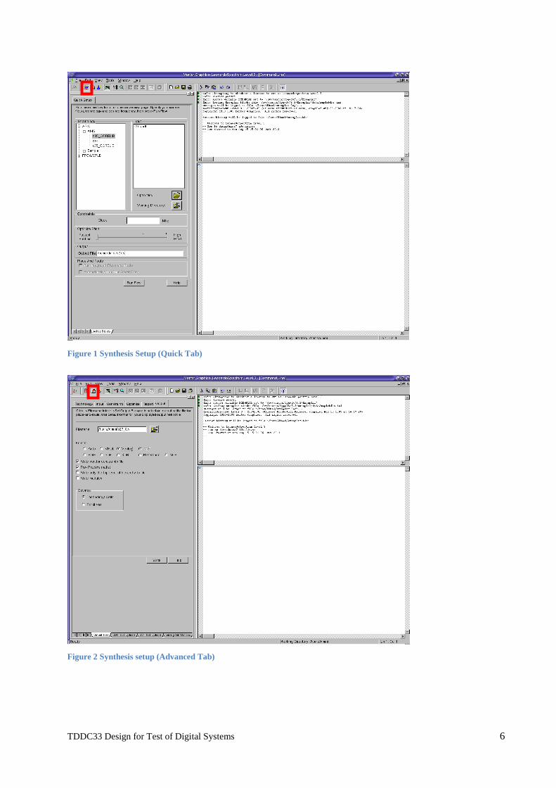
3. Synthesis
This chapter describes the synthesis procedure using Leonardo Spectrum from Mentor Graphics. It is
assumed that the initial preparations, described in the Chapter 2, have been made.
3.1. Input
A compiled VHDL-file
3.2. Output
A synthesized Verilog netlist
3.3. Synthesis procedure
Start the synthesis program from a command prompt
leonardo &
Click OK
In the Quick Setup tab
Select library file:
technology->ASIC->AMS->c35_CORELIB
Select input file
Input->Open files: Select the vhdl file (s27.vhd)
Select the name of the output file
s27.v
In the Advanced tab
Output -> Format->Verilog
In the Quick Setup tab
Check that the Optimize Effort is set to Fastest Runtime
Check that the output filename is correct
Start synthesis
Run Flow
Check the results from the synthesis in the Exemplar.log file
Check that the Verilog file (s27.v) was generated
TDDC33 Design for Test of Digital Systems 6
Figure 1 Synthesis Setup (Quick Tab)
Figure 2 Synthesis setup (Advanced Tab)
TDDC33 Design for Test of Digital Systems 7
4. Design for test using DFTAdvisor
This chapter describes how to perform scan chain insertion using DFTAdvisor tool from Mentor
Graphics.
4.1. Input
A design netlist (Verilog netlist)
Library file
4.2. Output
A new design netlist
ATPG setup files (dofile and procedure file)
4.3. Starting DFTAdvisor
Invoke DFTAdvisor from the command prompt
dftadvisor netlist_file –lib c35_CORELIB.ATPG
Note! The command is issued from a working directory that contains both the netlist_file and the
library file (c35_CORELIB.ATPG)
By default, the tool enters the SETUP mode. In this mode, the user can give further inputs to the tool
regarding the design that is provided, i.e. specify the primary inputs and outputs, specify clocks etc.
The tool is able to directly identify the primary inputs and outputs, but further inputs are required to
specify the clocks. To check the primary inputs and outputs that the tool has identified try the
following commands:
report primary inputs
report primary outputs
Next, we present how to specify clocks.
4.4. Circuit Setup
To specify the clocks, issue the following command:
add clocks off_state pin_pathname
where off_state represents the pin value (0 or 1) that results in a scan element’s clock input being at its
inactive state (for latches) or state prior to a capturing transition (for edge-triggered devices), and
pin_pathname represents a primary input pin that is to be assigned as a clock pin.
Example:
add clocks 0 CLK
Once all clocks are added, the circuit setup is completed, and we can continue working with the tool
and insert scan chains. To do that, we need to switch the system mode to DFT. We set the new system
mode by issuing the following command:
set system mode dft
4.5. Test Synthesis
In this section, we provide the commands that are required to insert scan chains into your design using
DFTAdvisor. Regarding scan chain insertion, we will describe the steps to perform a full scan
insertion, where all scannable elements are connected in a single scan chain, and partial scan
insertion where a number of scannable elements are stitched in a single chain.
TDDC33 Design for Test of Digital Systems 8
4.5.1 Full Scan Insertion
To setup full scan insertion run the following commands:
setup scan identification full_scan
run
After running these commands, in the command window you will get a brief report stating the number
of sequential elements that were identified in your design and how many of them have been converted
into scan cells. Next, we insert the test logic in the design by issuing the following command:
insert test logic
This command adds the new primary inputs and outputs to the circuit, replaces the sequential
elements into scan cells, and connects the scan cells in a single chain. To save the modified design,
you use the command:
write netlist filename
The new design has the scan chains included. To be able to run an ATPG for the scannable design,
there are some further inputs that are to be given to the ATPG tool (FastScan in this case) so that it
can identify the presence of the scan chains, and get to know how the scan operations are to be
performed. This information is included in the ATPG setup files (the procedure file and the dofile).
To save these files, use the following command:
write atpg setup basename
After running this command, two files are generated: basename.testproc (a file that contains the
information of how to perform the scan operations) and basename.dofile (a file that informs the
ATPG tool for the existence of scan circuitry in the design)
4.5.2 Partial Scan Insertion
To add partial scan, you need to first write a configuration file, where you explicitly select how many
and which memory elements to be converted into scan cells and connected in a scan chain. Note that
this you do manually, due to the lack of the tool to automatically run partial scan insertion. In the ideal
case, when a tool supports automatic partial scan insertion, the tool can select the specified number of
memory elements, which is given by the user as a number or maybe a percentage, by applying some
algorithm and performing some analysis so that it selects only “the most important” memory elements
to be converted into scan cells. For example, SCOAP can be used to identify which memory elements
are the best to be converted into scan cells and connected in a scan chain, so that the fault coverage is
maximized. Next, we describe how to write this configuration file to perform partial scan insertion.
The configuration file is a text file that contains lines, each of them with three parameters:
instance_pathname cell_id chain_id
instance_pathname - A string that specifies the name of the non-scan cell that you want DFTAdvisor
to put in the scan chain. To find instance_pathname open the netlist file and read its contents.
cell_id - An integer that specifies the placement of the instance_pathname in relation to other
instance_pathnames. DFTAdvisor places the instance having the smallest cell_id closest to the scan
chain output. All instances in the same chain must have unique cell_ids.
chain_id - An integer that specifies the scan chain in which you want DFTAdvisor to place the
instance_pathname. DFTAdvisor places instances with the same chain_id in the same chain.

TDDC33 Design for Test of Digital Systems 9
Once you have prepared the configuration file you only need to insert the test logic that is specified
there. To do this, use the following command:
insert test logic config_file
where config_file stands for the configuration file that you have written. Next you need to do, is to
write the netlist file and the atpg setup files, as described in the previous section.
TDDC33 Design for Test of Digital Systems 10
5. Fault Coverage Analysis and Test Pattern Generation using FastScan
This chapter describes the fault coverage analysis and test pattern generation process using FastScan
from Mentor Graphics. It is assumed that the initial preparations, described in Chapter 2, have been
made.
5.1. Input
A design netlist (Verilog netlist)
Library file
External test patterns (optional)
Command files: dofile and testproc file (optional)
5.2. Output
Test patterns
Fault coverage
5.3. Writing test patterns
Manually crafted test patterns should be written in a text file using the following format:
Combinational design (c17 design)
ASCII_PATTERN_FILE_VERSION = 2;
SETUP =
declare input bus "PI" = "/INP[0]", "/INP[1]", "/INP[2]", "/INP[3]",
"/INP[4]";
declare output bus "PO" = "/OUTP[0]", "/OUTP[1]";
end;
SCAN_TEST =
pattern = 0;
force "PI" "10010" 0;
measure "PO" "00" 1;
pattern = 1;
force "PI" "10010" 0;
measure "PO" "00" 1;
end;
TDDC33 Design for Test of Digital Systems 11
Sequential design (could be the s27 design)
ASCII_PATTERN_FILE_VERSION = 2;
SETUP =
declare input bus "PI" = "/INP[0]", "/INP[1]", "/INP[2]", "/INP[3]",
"/H";
declare output bus "PO" = "/OUTP[0]";
clock "/H" =
off_state = 0;
pulse_width = 1;
end;
end;
SCAN_TEST =
pattern = 0 clock_sequential ;
force "PI" "01110" 0;
pulse "/H" 1;
force "PI" "11010" 2;
measure "PO" "1" 3;
pattern = 1 clock_sequential ;
force "PI" "01010" 0;
pulse "/H" 1;
force "PI" "10110" 2;
measure "PO" "1" 3;
end;
5.4. Starting FastScan
To invoke FastScan use the following command:
fastscan netlist_file –lib c35_CORELIB.ATPG
By default, the tool enters the SETUP system mode, where you can provide more inputs to the tool
regarding the design for which you intend to perform fault simulation or want to run automatic test
pattern generation.
5.5. Circuit setup
If you are about to work with a sequential design, then you are supposed to specify which of the
primary inputs represent the clock pins. To specify clocks, use the following command:
add clocks off_state pin_pathname
where off_state represents the pin value (0 or 1) that results in a scan element’s clock input being at its
inactive state (for latches) or state prior to a capturing transition (for edge-triggered devices), and
pin_pathname represents a primary input pin that is to be assigned as a clock pin.
Example:
add clocks 0 CLK

TDDC33 Design for Test of Digital Systems 12
If you are about to work with a design that contains scan chains, and you want the ATPG tool to use
these test feature while generating the patterns, then you need to provide the dofile to the tool by
issuing the following command:
dofile filename.dofile
Once you are done with the circuit setup, you can continue further with either running fault
simulation, in which case you should switch to the FAULT system mode, or running the ATPG
process, in which case you should switch to the ATPG system mode. Switching the system mode is
done by using the following command:
set system mode $SM
where $SM denotes one of the following system modes: SETUP, GOOD, FAULT and ATPG.
5.6. Fault simulation
To perform fault simulation, you need to make sure that you have set the system mode to FAULT.
Before you run fault simulation, you need to specify the type of faults that you would like to be
simulated and you should add those faults in the fault list which will later be used by the tool to
identify which of them have been detected using the set of test patterns that you supply to the tool. To
add faults in the fault list, use the following command:
add faults -all -stuck_at 01
The given command adds all stuck_at faults for the provided netlist, meaning that at each fault site
(each net in the netlist) it considers both the stack_at 1 and stuck_at 0 faults. Given this fault list
during the fault simulation the tool will try to identify which of those faults are covered by the
supplied test pattern set. To observe which are the faults that have been added in the faults list, what is
their type and where are the fault sites in your netlist, you can use the following command:
report faults
To supply your own test pattern set, you should use the following command:
set pattern source external filename
Note! We assume that you have already created a test pattern file, using the instructions presented
earlier in this tutorial (see 5.3. Writing test patterns).
Once you have added the required faults in the fault list and have supplied a set of test patterns, you
perform the fault simulation by using the following command:
run
To get a detailed report about the fault coverage, use the following command
report statistics
5.7. Test pattern generation
To perform test pattern generation, you need to make sure that you have set the system mode to
ATPG. The next step is to add all the faults in the fault list, so that the tool can later generate test
patterns for detecting the faults that are present in the fault list. Here is the set of commands that you
should issue in order to generate test patterns.
add faults -all -stuck_at 01
create patterns
In the reported statistics you will be able to see what is the fault coverage for the generated test
patterns.

TDDC33 Design for Test of Digital Systems 13
5.8. Results and analysis
The following metrics are reported after running test pattern generation or fault simulation. Here is a
brief description for each of them.
Test Coverage - percentage of all testable faults that are detected by the patterns.
Fault Coverage - percentage of all faults both testable and untestable that are detected by the
patterns.
ATPG effectiveness percentage - a measure of the ability of the ATPG tool to either provide a test
to detect a fault, or prove that a test cannot be created.
TDDC33 Design for Test of Digital Systems 14
6. Test point insertion in VHDL
This chapter describes how the testability of a design can be improved by inserting test points. It is
assumed that the VHDL description of a design is available.
6.1. Input
A design described in VHDL
6.2. Output
A new design with test points.
6.3. Inserting test points
Add the new input and output ports in the ENTITY block
Add new signals in the ARCHITECTURE block (if needed)
Modify the design (introduction of new gates may be required) such that the new ports are
used to control and observe the “hard-to-test” parts of the design.
Please refer to Appendix A for an example of VHDL code with inserted test points.

TDDC33 Design for Test of Digital Systems 15
7. Board test using Boundary Scan (IEEE 1149.1)
This chapter describes the boundary scan board test methodology. For the board test programming
and test, a program called Trainer1149 from Testonica Lab is used.
7.1. Input
A board design, which consists of one bsdl-file for each chip and another file that contains a list of
connections between the chips.
7.2. Output
A test program.
7.3. Starting Trainer1149
Verify that the current installed version of java is 1.6 or higher
java –version
module add prog/jdk/1.6
Start the Trainer1149 program
java –jar trainer1149.jar &
Select an existing project or make a new project
7.4. How to use Trainer1149
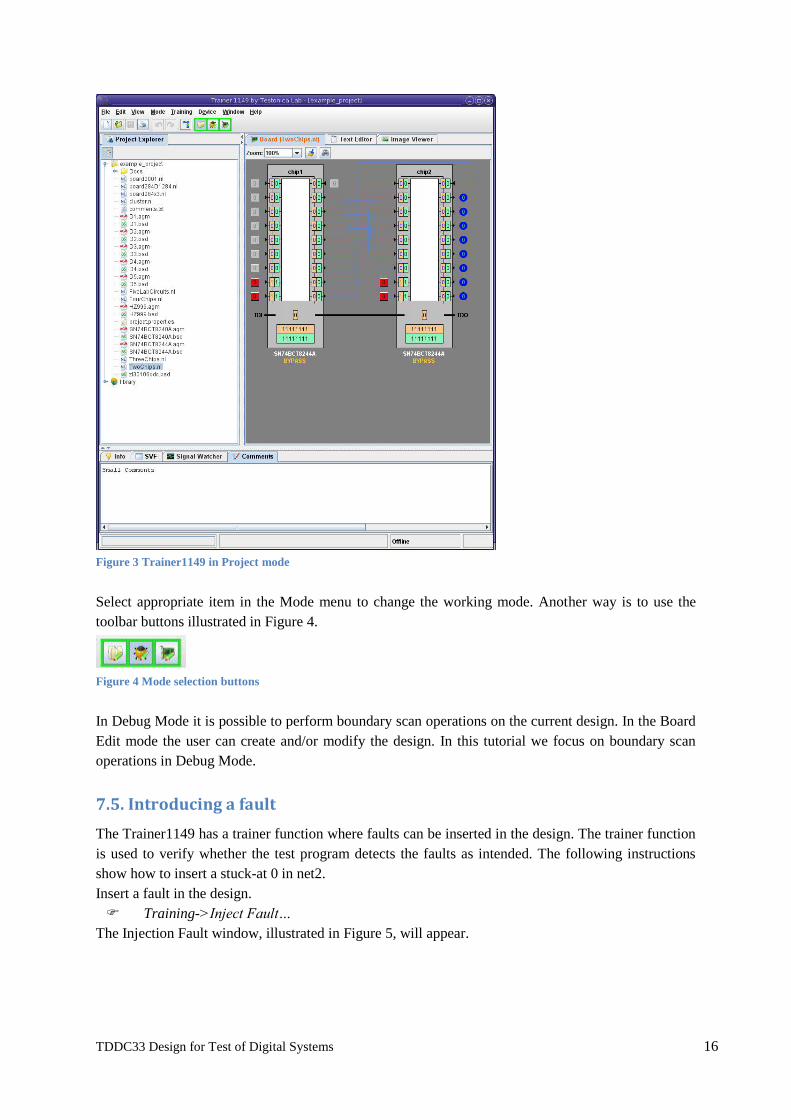
The Trainer1149 program has three different modes, Project Mode, Debug Mode, and Board Edit
Mode. The Trainer1149 program will start in the project mode, which allows you to view and modify
the board layout. In Figure 3, the twochips.nl netlist has been chosen in the Project Explorer.
TDDC33 Design for Test of Digital Systems 16
Figure 3 Trainer1149 in Project mode
Select appropriate item in the Mode menu to change the working mode. Another way is to use the
toolbar buttons illustrated in Figure 4.
Figure 4 Mode selection buttons
In Debug Mode it is possible to perform boundary scan operations on the current design. In the Board
Edit mode the user can create and/or modify the design. In this tutorial we focus on boundary scan
operations in Debug Mode.
7.5. Introducing a fault
The Trainer1149 has a trainer function where faults can be inserted in the design. The trainer function
is used to verify whether the test program detects the faults as intended. The following instructions
show how to insert a stuck-at 0 in net2.
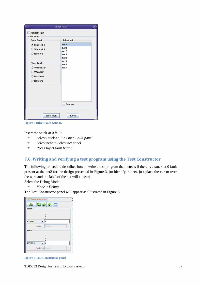
Insert a fault in the design.
Training->Inject Fault…
The Injection Fault window, illustrated in Figure 5, will appear.
TDDC33 Design for Test of Digital Systems 17
Figure 5 Inject Fault window
Insert the stuck-at 0 fault.
Select Stuck-at 0 in Open Fault panel.
Select net2 in Select net panel.
Press Inject fault button.
7.6. Writing and verifying a test program using the Test Constructor
The following procedure describes how to write a test program that detects if there is a stuck-at 0 fault
present at the net2 for the design presented in Figure 3. (to identify the net, just place the cursor over
the wire and the label of the net will appear)
Select the Debug Mode
Mode->Debug
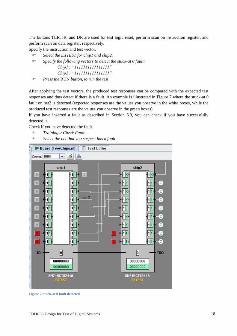
The Test Constructor panel will appear as illustrated in Figure 6.
Figure 6 Test Constructor panel
TDDC33 Design for Test of Digital Systems 18
The buttons TLR, IR, and DR are used for test logic reset, perform scan on instruction register, and
perform scan on data register, respectively.
Specify the instruction and test vector.
Select the EXTEST for chip1 and chip2.
Specify the following vectors to detect the stuck-at 0 fault:
Chip1 : “1111111111111111”
Chip2 : “1111111111111111”
Press the RUN button, to run the test
After applying the test vectors, the produced test responses can be compared with the expected test
responses and thus detect if there is a fault. An example is illustrated in Figure 7 where the stuck-at 0
fault on net2 is detected (expected responses are the values you observe in the white boxes, while the
produced test responses are the values you observe in the green boxes).
If you have inserted a fault as described in Section 6.3, you can check if you have successfully
detected it.
Check if you have detected the fault.
Training->Check Fault…
Select the net that you suspect has a fault
Figure 7 Stuck-at 0 fault detected
net 2
TDDC33 Design for Test of Digital Systems 19
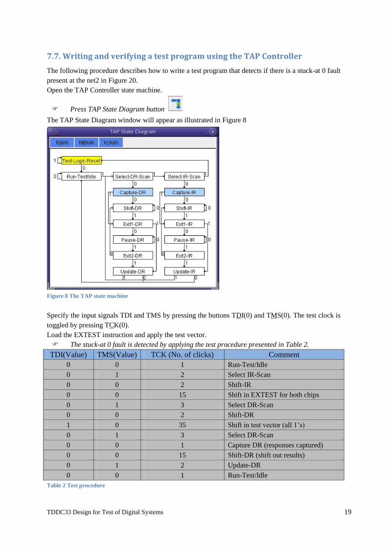
7.7. Writing and verifying a test program using the TAP Controller
The following procedure describes how to write a test program that detects if there is a stuck-at 0 fault
present at the net2 in Figure 20.
Open the TAP Controller state machine.
Press TAP State Diagram button
The TAP State Diagram window will appear as illustrated in Figure 8
Figure 8 The TAP state machine
Specify the input signals TDI and TMS by pressing the buttons TDI(0) and TMS(0). The test clock is
toggled by pressing TCK(0).
Load the EXTEST instruction and apply the test vector.
The stuck-at 0 fault is detected by applying the test procedure presented in Table 2.
TDI(Value) TMS(Value) TCK (No. of clicks) Comment
0 0 1 Run-Test/Idle
0 1 2 Select IR-Scan
0 0 2 Shift-IR
0 0 15 Shift in EXTEST for both chips
0 1 3 Select DR-Scan
0 0 2 Shift-DR
1 0 35 Shift in test vector (all 1’s)
0 1 3 Select DR-Scan
0 0 1 Capture DR (responses captured)
0 0 15 Shift-DR (shift out results)
0 1 2 Update-DR
0 0 1 Run-Test/Idle
Table 2 Test procedure
TDDC33 Design for Test of Digital Systems 20
Appendix A S27_TP VHDL Description
---------------------------------------------------------------------------------------------
--This file is modified by Anders Larsson
--Increased testability by introducing a new control point.
--More control and/or observable points should be added to further increase the testability.
---------------------------------------------------------------------------------------------
library IEEE;
use IEEE.std_logic_1164.all;
use work.all;
ENTITY s27_bench IS
PORT (
--Add a new input
INP: in std_ulogic_vector(0 to 4);
OUTP : out std_ulogic_vector(0 to 0);
H : in std_ulogic
);
END s27_bench ;
ARCHITECTURE structural OF s27_bench IS
component andg
generic (tpd_hl : time;
tpd_lh : time);
port (in1, in2 : std_logic;
out1 : out std_logic);
end component;
component org
generic (tpd_hl : time;
tpd_lh : time);
port (in1, in2 : std_logic;
out1 : out std_logic);
end component;
component xorg
generic (tpd_hl : time;
tpd_lh : time);
port (in1, in2 : std_logic;
out1 : out std_logic);
end component;
component xnorg
generic (tpd_hl : time;
tpd_lh : time);
port (in1, in2 : std_logic;
out1 : out std_logic);
end component;
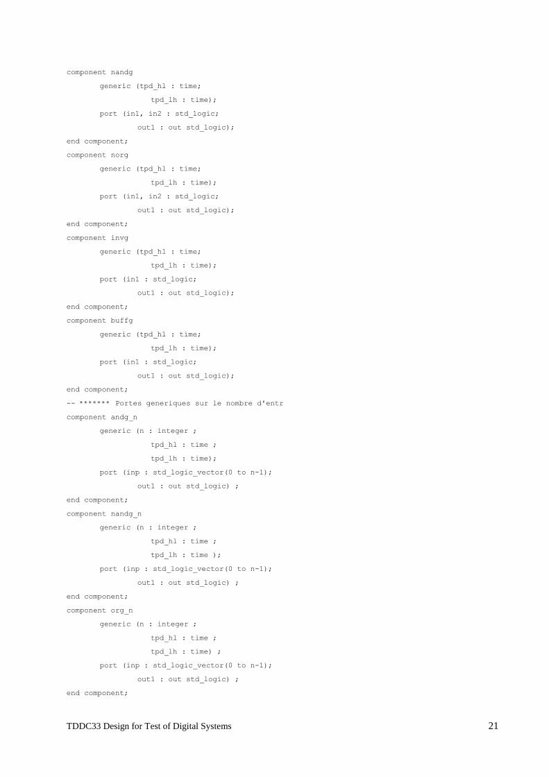
TDDC33 Design for Test of Digital Systems 21
component nandg
generic (tpd_hl : time;
tpd_lh : time);
port (in1, in2 : std_logic;
out1 : out std_logic);
end component;
component norg
generic (tpd_hl : time;
tpd_lh : time);
port (in1, in2 : std_logic;
out1 : out std_logic);
end component;
component invg
generic (tpd_hl : time;
tpd_lh : time);
port (in1 : std_logic;
out1 : out std_logic);
end component;
component buffg
generic (tpd_hl : time;
tpd_lh : time);
port (in1 : std_logic;
out1 : out std_logic);
end component;
-- ******* Portes generiques sur le nombre d'entr
component andg_n
generic (n : integer ;
tpd_hl : time ;
tpd_lh : time);
port (inp : std_logic_vector(0 to n-1);
out1 : out std_logic) ;
end component;
component nandg_n
generic (n : integer ;
tpd_hl : time ;
tpd_lh : time );
port (inp : std_logic_vector(0 to n-1);
out1 : out std_logic) ;
end component;
component org_n
generic (n : integer ;
tpd_hl : time ;
tpd_lh : time) ;
port (inp : std_logic_vector(0 to n-1);
out1 : out std_logic) ;
end component;

TDDC33 Design for Test of Digital Systems 22
component norg_n
generic (n : integer ;
tpd_hl : time ;
tpd_lh : time) ;
port (inp : std_logic_vector(0 to n-1);
out1 : out std_logic) ;
end component;
component xorg_n
generic (n : integer ;
tpd_hl : time ;
tpd_lh : time) ;
port (inp : std_logic_vector(0 to n-1);
out1 : out std_logic) ;
end component;
component xnorg_n
generic (n : integer ;
tpd_hl : time ;
tpd_lh : time) ;
port (inp : std_logic_vector(0 to n-1);
out1 : out std_logic) ;
end component;
component DFFC
generic (tpd_hl : time;
tpd_lh : time);
port (DFFC,H,C : std_logic;
Q : out std_logic);
end component;
component DFF
generic (tpd_hl : time;
tpd_lh : time);
port (D,H : std_logic;
Q : out std_logic);
end component;
component TFFC
generic (tpd_hl : time;
tpd_lh : time);
port (T,H,C : std_logic;
Q : out std_logic);
end component;
signal INTERP : std_ulogic_vector(0 to 11):=(others=>'0') ;
signal OUTPI : std_ulogic_vector(OUTP'range):=(others=>'0') ;
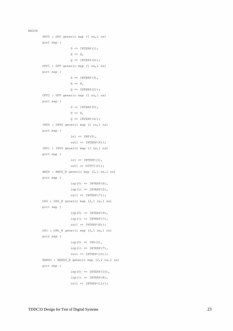
TDDC33 Design for Test of Digital Systems 23
BEGIN
DFF0 : DFF generic map (1 ns,1 ns)
port map (
D => INTERP(1),
H => H,
Q => INTERP(0));
DFF1 : DFF generic map (1 ns,1 ns)
port map (
D => INTERP(3),
H => H,
Q => INTERP(2));
DFF2 : DFF generic map (1 ns,1 ns)
port map (
D => INTERP(5),
H => H,
Q => INTERP(4));
INV0 : INVG generic map (1 ns,1 ns)
port map (
in1 => INP(0),
out1 => INTERP(6));
INV1 : INVG generic map (1 ns,1 ns)
port map (
in1 => INTERP(3),
out1 => OUTPI(0));
AND0 : ANDG_N generic map (2,1 ns,1 ns)
port map (
inp(0) => INTERP(6),
inp(1) => INTERP(2),
out1 => INTERP(7));
OR0 : ORG_N generic map (2,1 ns,1 ns)
port map (
inp(0) => INTERP(9),
inp(1) => INTERP(7),
out1 => INTERP(8));
OR1 : ORG_N generic map (2,1 ns,1 ns)
port map (
inp(0) => INP(3),
inp(1) => INTERP(7),
out1 => INTERP(10));
NAND0 : NANDG_N generic map (2,1 ns,1 ns)
port map (
inp(0) => INTERP(10),
inp(1) => INTERP(8),
out1 => INTERP(11));
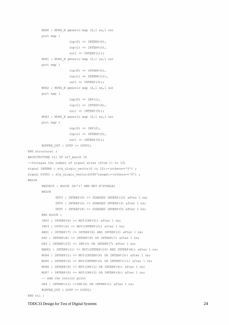
TDDC33 Design for Test of Digital Systems 24
NOR0 : NORG_N generic map (2,1 ns,1 ns)
port map (
inp(0) => INTERP(6),
inp(1) => INTERP(3),
out1 => INTERP(1));
NOR1 : NORG_N generic map (2,1 ns,1 ns)
port map (
inp(0) => INTERP(0),
inp(1) => INTERP(11),
out1 => INTERP(3));
NOR2 : NORG_N generic map (2,1 ns,1 ns)
port map (
inp(0) => INP(1),
inp(1) => INTERP(4),
out1 => INTERP(9));
NOR3 : NORG_N generic map (2,1 ns,1 ns)
port map (
inp(0) => INP(2),
inp(1) => INTERP(9),
out1 => INTERP(5));
BUFFER_OUT : OUTP <= OUTPI;
END structural ;
ARCHITECTURE rtl OF s27_bench IS
--Increase the number of signal wires (from 11 to 12)
signal INTERP : std_ulogic_vector(0 to 12):=(others=>'0') ;
signal OUTPI : std_ulogic_vector(OUTP'range):=(others=>'0') ;
BEGIN
REGVECT : BLOCK (H='1' AND NOT H'STABLE)
BEGIN
DFF3 : INTERP(0) <= GUARDED INTERP(12) after 1 ns;
DFF4 : INTERP(2) <= GUARDED INTERP(3) after 1 ns;
DFF5 : INTERP(4) <= GUARDED INTERP(5) after 1 ns;
END BLOCK ;
INV2 : INTERP(6) <= NOT(INP(0)) after 1 ns;
INV3 : OUTPI(0) <= NOT(INTERP(3)) after 1 ns;
AND1 : INTERP(7) <= INTERP(6) AND INTERP(2) after 1 ns;
OR2 : INTERP(8) <= INTERP(9) OR INTERP(7) after 1 ns;
OR3 : INTERP(10) <= INP(3) OR INTERP(7) after 1 ns;
NAND1 : INTERP(11) <= NOT(INTERP(10) AND INTERP(8)) after 1 ns;
NOR4 : INTERP(1) <= NOT(INTERP(6) OR INTERP(3)) after 1 ns;
NOR5 : INTERP(3) <= NOT(INTERP(0) OR INTERP(11)) after 1 ns;
NOR6 : INTERP(9) <= NOT(INP(1) OR INTERP(4)) after 1 ns;
NOR7 : INTERP(5) <= NOT(INP(2) OR INTERP(9)) after 1 ns;
-- Add the control point
OR4 : INTERP(12) <=INP(4) OR INTERP(1) after 1 ns;
BUFFER_OUT : OUTP <= OUTPI;
END rtl ;

TDDC33 Design for Test of Digital Systems 25
References
[1] http://asic.austriamicrosystems.com/databooks/c35/databook_c35_33/, April 2006.