laboratory implementations of pmsm drive in hybrid
TRANSCRIPT
Scholars' Mine Scholars' Mine
Masters Theses Student Theses and Dissertations
Spring 2012
Laboratory implementations of PMSM drive in hybrid electric Laboratory implementations of PMSM drive in hybrid electric
vehicles applications vehicles applications
Amir E. Saad
Follow this and additional works at: https://scholarsmine.mst.edu/masters_theses
Part of the Electrical and Computer Engineering Commons
Department: Department:
Recommended Citation Recommended Citation Saad, Amir E., "Laboratory implementations of PMSM drive in hybrid electric vehicles applications" (2012). Masters Theses. 5136. https://scholarsmine.mst.edu/masters_theses/5136
This thesis is brought to you by Scholars' Mine, a service of the Missouri S&T Library and Learning Resources. This work is protected by U. S. Copyright Law. Unauthorized use including reproduction for redistribution requires the permission of the copyright holder. For more information, please contact [email protected].


LABORATORY IMPLEMENTATIONS OF PMSM DRIVE
IN HYBRID ELECTRIC VEHICLES APPLICATIONS
by
AMIR E. SAAD
A THESIS
Presented to the Faculty of the Graduate School of the
MISSOURI UNIVERSITY OF SCIENCE AND TECHNOLOGY
In Partial Fulfillment of the Requirements for the Degree
MASTER OF SCIENCE IN ELECTRICAL ENGINEERING
2012
Approved by
Jonathan W. Kimball, Advisor
Mehdi Ferdowsi
Keith Corzine

2012
Amir E. Saad
All Rights Reserved

iii
ABSTRACT
Field Programmable Gate Arrays (FPGAs) are one of the today’s most successful
technologies for developing systems that require real time operation and providing
additional flexibility to the designer. This research is focused on developing a control
board for a permanent magnet synchronous machine (PMSM) using an FPGA module.
The board is configured for individual use of an FPGA, digital signal processor (DSP) or
in combination to control the PMSM by generating the required Pulse Width Modulator
(PWM) to the inverter in order to drive and control the speed of the PMSM. Since, the
exact rotor position and speed are required to control the motor; a useful method is
developed digitally and implemented in the FPGA hardware module. The speed observer
(SO), in which the Hall effect signals were used to calculate the speed and the angle of
the rotor.
In this thesis, three different techniques of PWM generation were developed and
combined with rotor position and speed method. The project is implemented in Altera
FPGA using Quartus II software V11.0 with VHDL as the supporting language. The
design achieved high performance and accuracy of the detection estimation and control
scheme for the Permanent Magnet Synchronous Machine. Error and design analysis has
been done also.

iv
ACKNOWLEDGMENTS
I owe my utmost gratitude to my Advisor Dr. Jonathan Kimball, who has the
attitude and the substance of a genius: his encouragement, guidance and support from the
initial to the final level enabled me to develop and understand the subject, for inspiring
and motivating me to overcome all the obstacles in the completion of this work, and for
providing the financial support to me and my family through this wonderful period.
I would like to thank my committee members; Dr. Mehdi Ferdowsi and Dr. Keith
Corzine, for helping me walk through my academic knowledge and technical
participation at the DOE project, providing me the encouragement to achieve the
maximum success.
I would like to thank my parents, Elshaikh Saad and Asmaa Saad and my brother
Mohamed and also extend my sincere thanks and appreciation to my little family, my
dearest wife Hadeel Abdalla and balsam of my life my daughter Leen Saad for their
support, patience, and encouragement during these years.
I would like to thank my friends, classmates, the faculty staff, and everyone who
helped or encouraged me during my whole life.
Lastly, thank you to the Department of Energy and the Missouri S&T research
board for their financial support. This research was sponsored by the Department of
Energy under grant DE-EE0002012.

v
TABLE OF CONTENTS
Page
ABSTRACT ....................................................................................................................... iii
ACKNOWLEDGMENTS ................................................................................................. iv
LIST OF ILLUSTRATIONS ............................................................................................ vii
LIST OF TABLES ............................................................................................................. ix
NOMENCLATURE ........................................................................................................... x
SECTION
1. INTRODUCTION ...................................................................................................... 1
1.1. BACKGROUND ................................................................................................ 1
1.2. PROPOSED APPROACH .................................................................................. 1
1.3. LITERATURE REVIEW ................................................................................... 4
1.4. THESIS OUTLINE ............................................................................................. 7
2. SIGNAL PROCESSING AND CONTROL BOARD ............................................... 8
2.1. INTRODUCTION .............................................................................................. 8
2.2. SIGNAL CONDITIONING CIRCUIT............................................................... 8
2.3. FILTER CIRCUIT ............................................................................................ 10
2.4. LEVEL SHIFTERS .......................................................................................... 11
2.5. ANALOG TO DIGITAL CONVERTERS ....................................................... 12
2.6. ISOLATOR CIRCUIT ...................................................................................... 14
2.7. CAN TRANSCEIVER CIRCUIT..................................................................... 14
2.8. DIFFERENTIAL INPUT CIRCUIT................................................................. 15
2.9. DSP CIRCUIT .................................................................................................. 16
2.10. FPGA CIRCUIT ............................................................................................. 17
2.11. POWER SUPPLY BOARD ............................................................................ 19
2.12. PULL-UP RESISTOR CIRCUIT ................................................................... 21
2.13. ERRATA......................................................................................................... 22
3. PULSE WIDTH MODULATOR ............................................................................. 23
3.1. INTRODUCTION ............................................................................................ 23
3.2. DIGITAL PWM GENRATION TYPES .......................................................... 23

vi
3.2.1. Up-Mode Counter ................................................................................... 24
3.2.2. Down-Mode Counter .............................................................................. 24
3.2.3. Up-Down Mode Counter ........................................................................ 25
3.2.4. PWM with Dead-Band ........................................................................... 26
4. PMSM ROTOR POSITION MEASUREMENT ..................................................... 30
4.1. INTRODUCTION ............................................................................................ 30
4.1.1. Optical Encoder ...................................................................................... 30
4.1.2. Resolver .................................................................................................. 31
4.1.3. Full Observer .......................................................................................... 31
4.1.4. Hall Effect Sensors ................................................................................. 32
4.2. HYBRID SPEED OBSERVER ........................................................................ 33
5. RESULTS AND SYSTEM VALIDATION ............................................................ 43
5.1. MODELSIM RESULTS ................................................................................... 43
5.2. HARDWARE RESULTS ................................................................................. 46
6. CONCLUSION AND FUTURE SCOPE ................................................................. 51
APPENDICES
A. PRINTED CIRCUIT BOARDS DESIGN………………………………………...52
B. VHDL CODES OF THE DESIGN………………………………………………...71
BIBLIOGRAPHY ............................................................................................................. 88
VITA ................................................................................................................................ 91

vii
LIST OF ILLUSTRATIONS
Page
Figure 1.1. PCB0021 Control Board.................................................................................. 3
Figure 1.2. The Control Board and the Inverter. ................................................................ 3
Figure 2.1. Gains and Offset Circuit. ................................................................................. 8
Figure 2.2. Generic Sallen Key Filter Topology.............................................................. 10
Figure 2.3. CMOS Hex Voltage –Level Shifter. ............................................................. 12
Figure 2.4. AD7276 Block Diagram ................................................................................ 13
Figure 2.5. AD7329 Block Diagram ................................................................................ 13
Figure 2.6. ADUM1412 Block Diagram ......................................................................... 14
Figure 2.7. 65HVD251Funcional Diagram ..................................................................... 15
Figure 2.8. Differential Amplifier Circuit........................................................................ 16
Figure 2.9. TMS320F28335. ............................................................................................ 17
Figure 2.10. Structure of the FPGA. ................................................................................ 18
Figure 2.11. Altera Design Flow Chart ............................................................................ 19
Figure 2.12. PES and PET Type Connectors ................................................................... 20
Figure 2.13. PCB0025...................................................................................................... 20
Figure 2.14. Pull-up Resistor for Open Collector Configuration..................................... 21
Figure 3.1. PWM Block Diagram. ................................................................................... 23
Figure 3.2. Up Mode Counter. ......................................................................................... 24
Figure 3.3. Down Mode Counter. .................................................................................... 25
Figure 3.4. Up-Down Mode Counter. .............................................................................. 25
Figure 3.5. Signals of Interest. ......................................................................................... 26
Figure 3.6. PWM Schematic Diagram. ............................................................................ 28
Figure 4.1. Optical Encoder ............................................................................................. 30
Figure 4.2. Resolver Schematic ....................................................................................... 31
Figure 4.3. Full Adaptive Observer ................................................................................. 32
Figure 4.4. Three Hall Effect Sensors and Their Related Signals ................................... 33
Figure 4.5. High-Performance BLDC .............................................................................. 34
Figure 4.6. Hybrid Observer Bounding Functions........................................................... 36

viii
Figure 4.7. Hybrid Observer Block Diagram [26]. .......................................................... 39
Figure 4.8. Speed Observer Schematic in VHDL. ........................................................... 40
Figure 4.9. PCB0006 Experiments Board........................................................................ 41
Figure 4.10. The Experiment dc Motor. .......................................................................... 42
Figure 5.1. The Simulation Results of the Up-Mode Counter. ........................................ 43
Figure 5.2. The Simulation Results of the Down-Mode Counter. ................................... 43
Figure 5.3. The Simulation Results of the Up-Down Counter. ....................................... 44
Figure 5.4. Screen Shot (1) for Parameters Results of the SO. ........................................ 44
Figure 5.5. Screen Shot (2) for Parameters Results of the SO. ........................................ 45
Figure 5.6. Screen Shot (3) for Parameters Results of the SO. ........................................ 45
Figure 5.7. Screen Shot (4) for Parameters Results of the SO. ........................................ 46
Figure 5.8. The Rising-Edge Counter Delay. .................................................................. 46
Figure 5.9. The Falling-Edge of the Fed Counter. ........................................................... 47
Figure 5.10. Hall Effect Signals. ...................................................................................... 47
Figure 5.11. The SO Output in 59.86 Hz Hall Effect Signals Input. ............................... 48
Figure 5.12. The Absolute Error vs. m Bits. .................................................................... 49
Figure 5.13. The Total Logic Elements vs. m Bits. ......................................................... 49
Figure 5.14. The sin(θrh) Output. ..................................................................................... 50
Figure 5.15. Zoom in Results of sin(θrh). ......................................................................... 50

ix
LIST OF TABLES
Page
Table 2.1. Maximum and Minimum Voltage Range. ........................................................ 9
Table 2.2. The Resistor Values for Fig. 2.1. ...................................................................... 9
Table 2.3. Capacitor and Resistor Values. ....................................................................... 11
Table 2.4. Power Modules and Corresponding Voltages. ............................................... 21
Table 4.1. Bounding Functions vs. Hall States ................................................................ 35
Table 4.2. State Transition Points .................................................................................... 35
Table 4.3. Initial Conditions ............................................................................................ 37
Table 4.4. The Motor Parameters. ................................................................................... 42

x
NOMENCLATURE
Symbol Description
HEVs Hybrid Electric Vehicles
EMs Electric Motors
CAN Computer Automotive Network
RTDC Resolver-to-Digital Converter
SO Speed Observer
PMSM Permanent Magnet Synchronous Machine
FPGA Field Programmable Gate Array
Q Quality factor
fc Cutoff frequency
i Observed current
v Observed voltage
ha, hb, hc Hall effect sensor signals
rω Rotor angular speed
r Rotor estimated speed
rθ Rotor electrical position

1
1. INTRODUCTION
1.1. BACKGROUND
Electric motors (EMs) and generators are the primary workhorses in hybrid-
electric vehicles (HEVs). The generators convert mechanical power from the engine
electrical power in order to charge the batteries and operate the motors. Then motors
produce the required torque to drive the wheels. There are many types of motors and
generators used in HEVs: induction, switched reluctance, and permanent magnet. Each
type requires the occurrence of a magnetic field. Reluctance and induction motors use an
external source to provide the magnetic field, while the permanent magnet motors use
permanent magnets for this purpose. The critical factors for these components are power,
efficiency, controllability, cost, and durability [1-3].
PMSMs have been generally used in the HEV over the last two decades because
of their high efficiency, high-power density and lack of a dc field winding in the rotor;
however, they are more expensive than alternatives [2]. It is usually accepted that precise
control of a PMSM requires exact rotor position and speed information. The methods to
detect the rotor position are basically divided into two categories. One is the rotor
position detection by a position sensor mounted on the machine rotor, and the other is a
sensor-less method based on indirect rotor position estimation techniques [3].
In this thesis, a control board for a PMSM is constructed with advanced electronic
techniques in order to offer the best type of control for a PMSM in a HEV application.
The board contains many different signal processing circuits in addition to the flexibility
of using microcontroller of FPGA module to apply different control applications. Rotor
speed and position scheme is implemented in the FPGA using VHDL language. The
method used is the Hall effect sensors to estimate the rotor speed and position [4].
1.2. PROPOSED APPROACH
In order to estimate the rotor position and control the PMSM, a signal processing
control board is necessary to study, investigate and apply many different control
techniques. The circuits in the board have been simulated using MATLAB SIMULINK
and SPICE for the sake of accuracy and stability of the system. Then CADSOFT EAGLE

2
PCB design software was used to layout the board. The board uses two different
technologies to control the motor: a digital signal processor (DSP) and a FPGA. The
Altera Cyclone II FPGA module delivers high performance and low power consumption
at a cost that rivals that of ASICs. Altera’s modules are supported by the easy-to-use and
Quartus II licensed or free Edition design software.
The control board has the capability of working in three modes, the DSP only, the
FPGA only, or the DSP-FPGA share mode. In the DSP mode only, all the signals are
forwarded towards the DSP for either generating a special signal such as PWM or reading
an external signal such as dc bus voltage, current sensors, or Hall effect signals to make
other control decisions. The FPGA is being developed to have the same functionality as
the DSP. Furthermore, these two devices can share all the control operation if needed,
due to the high performance of the FPGA which runs at 24 MHz in this particular module
or even up to 400 MHz in some other families.
Signal conditioning circuits are added to the board in order to offer the
compatibility for the DSP to read external signals from the inverter (Semikron Box),
current sensors or the dc bus. Another differential input circuit has been implemented in
case applications require different ground reference. Also, level shifter circuits from +3V
to +15V and +15V to +3V are needed to condition the PWM signals to be compatible
with the Inverter gates threshold or receive fault signals respectively.
Sallen-Key Filters were added to the board for converting signals from digital to
analog for monitoring some interesting parameters. Communication is very important in
this type of applications, thus, Computer Automotive Network (CAN) transceivers were
added to the board. For extra design flexibility, digital Input/Outputs and relay
contractors were added to the board for future uses. External Analog to Digital
Converters (ADCs) were added in case of the DSP ADCs failure and to speed up the
DSP’s processing by passing them through the FPGA. Another 16 channel serial ADC
was added to offer digital signal to the FPGA.
Figures 1.1 and 1.2 illustrate the control board block diagram and the real board
attached to the inverter screen shot.

3
Figure 1.1. PCB0021 Control Board.
Figure 1.2. The Control Board and the Inverter.
4
1.3. LITERATURE REVIEW
The existing literatures on the rotor speed and position estimation are studied in
this section along with literature that focuses in type of observing methods to estimate
these characteristics. A common type of motor that has been used in HEVs is the PMSM
[2]. Therefore, this literature will be around this type of a motor.
A proposal of self-sensing technique is proposed in [4]. The technique functions
in a manner similar to a resolver and resolver-to-digital converter (RTDC) sensing
system, in this technique the motor acts as the electromagnetic resolver and the power
converter applies carrier-frequency voltages to the stator which produce high-frequency
currents that proportional with position. The sensed currents are processed with a
heterodyning technique that provides a signal that is nearly proportional to the difference
between the actual rotor position and an estimated rotor position.
Another proposal of a self-sensing technique and high-frequency injection in [5]
is based on tracking observer to correct the limitation in [4]. This method uses a rotating
vector, a carrier signal, and a tracking observer. In this method, high-frequency injection
makes low and zero speed detection possible.
The authors in [6] proposed a FPGA based scheme in which the rotor position can
be estimated by using three symmetrical locked Hall effect position sensors. This scheme
is implemented using the Altera FPGA, by assuming the time interval between adjacent
changes Hall effect sensor signal is t and calculating the average electric angular
velocity rω is,
/ (3Δ )rω π t (1)
The estimated dynamic error is
2 2a
2 2 p
Dmax 2 2 2 2
π p aπδθ ω ω ω ω
a p (2)
5
Where a is the motor’s acceleration, p is the number of pole pair, and 2ω is the
angular velocity that corresponds to the switching point of the Hall interval.
A scheme of modeling and cosimulation of the PMSM control system using an
FPGA is proposed in [7], This method uses the Space Vector Pulse Width Modulator
(SVPWM), D-Q transformation and PI controller as a control scheme. During the design,
the cosimulation between the function model and the VHDL model has been
implemented. The cosimulation between the function model and VHDL model realizes
the timing and control simulation by using Link-for Modelsim® in MATLAB.
The high frequency signal injection method proposed in [8] to improve the
detection accuracy. A DSP (TMS320F2812) is used to implement this method and 4-pole
PMSM is selected as experiment subject. The position detection scheme shows high
accuracy and reduces the error.
Mathematical modeling of a PMSM and the flux-linkage observer is proposed in
[9]. The mathematical model is used to approximate the nonlinear system of PMSM. Due
to the present modification scheme with error-correction, the rotor position and machine
speed can be estimated; even in the transient state the system has the capability of the
smooth starting and reversing. In addition, the system with the flux-linkage is very robust
and can tolerate variations in PMSM parameters.
The Hall effect method proposed in [10]; uses a simple algorithm that combines
the measurements of a Hall effect sensor with a “sensorless” method. In this method, the
Hall effect position sensor is used instead of a resolver as the mechanical sensor, to allow
vector control of a PMSM with a sinusoidal back-EMF. As a Hall effect sensor provides
only six measurements per electrical turn, the position error between the actual rotor
position and the measured position can potentially reach 30° electrically. This error
affects the control performances and causes significant torque oscillations and over
currents, which are not suitable in transportation systems applications. This method is
easy to implement, but it can not offer continuous precise information of the rotor
position.
A Flux linkage method is proposed in [11] and uses the flux linkage signals to
calculate the rotor position based on trigonometric approximations. The flux linkage
signals can be measured by accessing the neutral point of the PMSM. Regarding the

6
software implementation, the PMSM is modeled in Maxwell, where the nonlinear
magnetic flux density B and the magnetic flux intensity curves are also considered.
Multiple geometric and saturation induced saliencies based on a stator-oriented
magnetic circuit approach is introduced in [12], it introduces a new modeling approach of
a nonlinear machine model. The advantage of this method is that all kinds of saliencies
that occur in the electrical machine can be considered simultaneously. Moreover,
modeling in the stator coordinates leads to a physically motivated explanation when the
cross saturation effect can occur in a PMSM.
The vector-tracking position observer is proposed [13], it is an improved approach
for estimating the rotor positions in PMSM drives with low-resolution Hall effect
sensors. A vector-tracking position observer in conjunction with a discrete Hall effect
sensor’s output signal has been proposed, which is similar to a phase-locked loop
structure. It consists of a position error detector, based on the vector cross product of the
unit back-electromotive-force vectors obtained from a stator electrical model, and a
proportional–integral type controller, to make the position error rapidly converge to zero.
This structure does not only compensate the misalignment effect of the Hall effect
sensors, but also enhance their transient operating capability. This structure allows the
proposed approach to provide useful position information even at and around zero speeds
where the vector-tracking correction loop cannot correctly operate. Above zero speeds,
the proposed approach provides the high-resolution position information, where the
position estimation error rapidly converges to zero regardless of the misalignment of
Hall's sensors and the excessive average-speed error, particularly speed transient
operation. Through the experiments during the steady-state, start-up, speed transient, and
load transient operations, the effectiveness and the dynamic performance of the proposed
approach have been evaluated and verified.
Most of the literature focuses on how to implement different techniques using
mathematical modeling through MATLAB SIMULINK and implement it into a
microcontroller. However, a few authors had tried to implement the algorithms in an
FPGA. Moreover, all the previous studies did not discuss the error analysis of the hybrid
speed observer in which the rotor speed and positions can be determine from the Hall
effect sensors' signals.

7
1.4. THESIS OUTLINE
This section deals with general introduction for the HEV and the importance of
the PMSM in the implementation also brief detail of the existing observation and
estimation of the rotor speed and angle and how these techniques can help on the control
of the motor.
Section 2 describes the control board implementation and the electronic related
circuits design configurations and calculations.
Section 3 provides an introduction to the Pulse Width Modulator and different
approaches of PWM signal generation by using the FPGA or Microcontroller.
Section 4 describes the Hybrid Speed Observer technique for detecting the rotor
speed and position using the Hall effect signals and the physical implementation in the
FPGA using the Quartus II software and the error analysis.
Section 5 presents the system validations after the implementation in the FPGA
and connecting the board to the PMSM. The results are presented in this section to show
the possibility of substituting the Microcontroller with an FPGA or sharing the
operations.
Section 6 presents the conclusions. Design problems and recommendations for
future research are also discussed in this chapter.
8
2. SIGNAL PROCESSING AND CONTROL BOARD
2.1. INTRODUCTION
The control board consists of 15 different circuit blocks. Each bock has been
developed and simulated using SIMULINK or PLECS before the physical
implementation to ensure desired results. Numerical calculations were used to determine
the right values for the components. All components were chosen based on cost,
efficiency, and minimum losses. This section of the thesis will explain the purpose of
each circuit associated with a step by step design calculation and circuit configuration.
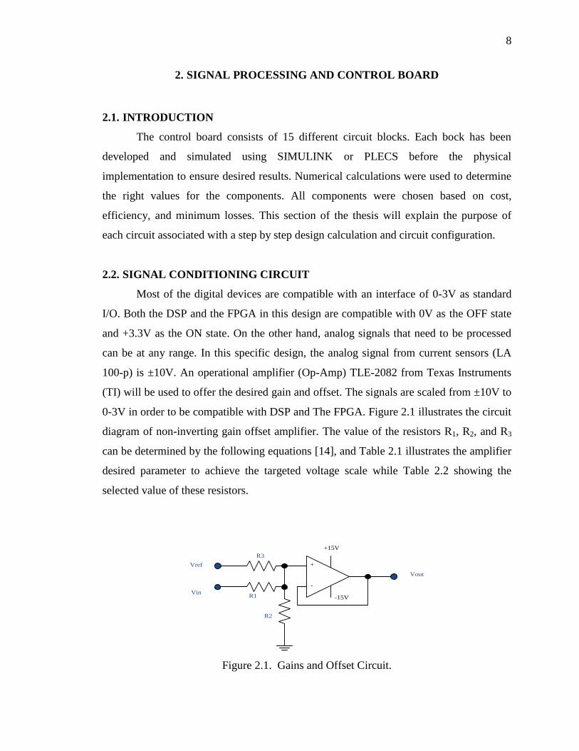
2.2. SIGNAL CONDITIONING CIRCUIT
Most of the digital devices are compatible with an interface of 0-3V as standard
I/O. Both the DSP and the FPGA in this design are compatible with 0V as the OFF state
and +3.3V as the ON state. On the other hand, analog signals that need to be processed
can be at any range. In this specific design, the analog signal from current sensors (LA
100-p) is ±10V. An operational amplifier (Op-Amp) TLE-2082 from Texas Instruments
(TI) will be used to offer the desired gain and offset. The signals are scaled from ±10V to
0-3V in order to be compatible with DSP and The FPGA. Figure 2.1 illustrates the circuit
diagram of non-inverting gain offset amplifier. The value of the resistors R1, R2, and R3
can be determined by the following equations [14], and Table 2.1 illustrates the amplifier
desired parameter to achieve the targeted voltage scale while Table 2.2 showing the
selected value of these resistors.
R3
R1
R2
+
-
Vref
Vin
Vout
+15V
-15V
Figure 2.1. Gains and Offset Circuit.

9
Table 2.1. Maximum and Minimum Voltage Range.
Vout,min 0V
Vout,max 3V
Vin,min -10V
Vin,max +10V
Vref +10V
m 0.15
b 1.5
out inV m V b (3)
1
1 2 3
1
Rm
1 1 1
R R R
(4)
3ref
1 2 3
1
Rb V
1 1 1
R R R
(5)
Table 2.2. The Resistor Values for Fig. 2.1.
R1 49.9 kΩ
R2 10.7 kΩ
R3 49.9 kΩ

10
2.3. FILTER CIRCUIT
Filter circuits usually are crucial and require precision. The Sallen Key filter is
very popular active filter topology. It is used to implement second order filters or higher
with different gain factor, high-quality factor, and simple configuration for the second-
order type and can be constructed with following equations from [15, 16]. Figure 2.2 [16]
illustrates the generic Sallen Key filter configuration.
+15V
-15V
+
-
C1
R1 R2
C2 Vout
Vin
Figure 2.2. Generic Sallen Key Filter Topology.
The cutoff frequency fc and the quality factor Q are
c
1 1 2 2
1f
2 R C R C
(6)
1 2 1 2
2 1 2
R R C CQ
C (R R )
(7)
For simplicity of the design, a good assumption is to equalize all the resistors.
1 2R R R (8)

11
This assumption simplifies the equations of the quality factor and the cutoff
frequency as follows.
1 2 1
2 2
C C C1Q
2C 2 C (9)
c
1 2
1f
2 R C C
(10)
1
o
2QC
R
(11)
2
o
1C
2RQ
(12)
In this design, the desired cutoff frequency is fc = 3 KHz and quality factor is Q =
0.6 for a better response. After using equations (9), (10), (11), and (12) the values of the
design are shown in Table 2.3.
Table 2.3. Capacitor and Resistor Values.
C1 142pF
C2 100pF
R 2.2kΩ
2.4. LEVEL SHIFTERS
The microcontroller and FPGA outputs are limited to +3.3V logic signal while the
inverter module needs about +15V to turn the gate of the insolated gate bipolar transistors

12
(IGBTs) on and also the fault signals that need to be interfaced to the DSP or FPGA are
+15V. A logic level shifting circuit is needed therefore; the CD4504B voltage level-
shifter from Texas Instruments consists of six circuits, which shift the input signals from
the VCC logic level to the VDD logic level. For example, to shift from TTL logic signals to
CMOS logic scale, the SELECT pin-13 input is at the VCC high logic state. And when the
SELECT pin is at low logic state “GND”, each circuit translates the signals from one
CMOS to another [17]. Figure 2.3 [17] illustrates the internal block diagram and the pin
out for CD4504B.
OUTLEVEL SHIFTER
TTL/CMOS
MODE SELECT
Vcc
IN
SELECT
Pin(3,5,7,9,11,14)
13
Vdd
Pin(2,4,6,10,12,15)
Vcc = Pin 1
Vdd= Pin 16
Vss= Pin 8
Figure 2.3. CMOS Hex Voltage –Level Shifter.
2.5. ANALOG TO DIGITAL CONVERTERS
The outputs of the current, voltage, and temperature sensors are analog. In order
to process these signals by using DSP, analog to digital converters are needed. Eight
AD7276 12-bit, high speed, and low power ADCs from Analog Devices are used to
convert the sensors' analog signals to digital signals in order to interface it to the DSP or
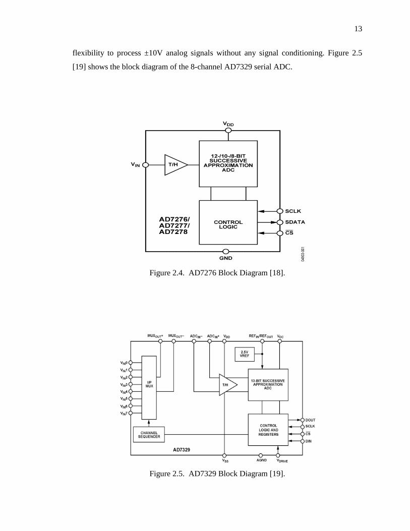
the FPGA [19]. Figure 2.4 [18] shows the block diagram of AD7276. Another serial
analog to digital converter AD7329 has been added to the design because of extra
13
flexibility to process ±10V analog signals without any signal conditioning. Figure 2.5
[19] shows the block diagram of the 8-channel AD7329 serial ADC.
Figure 2.4. AD7276 Block Diagram [18].
Figure 2.5. AD7329 Block Diagram [19].

14
2.6. ISOLATOR CIRCUIT
Isolator circuits are usually used when a certain signal needs to be transferred
from one circuit to another without any direct coupling, because these circuits may
operate at different voltage levels. This technique is used to decouple the board and the
Computer Automotive Network (CAN) a bus signal, ADUM1412 quad-channel digital
isolator from Analog Devices is used for this purpose. Figure 2.6 displays the block
diagram and the pin out of the ADUM1412.
Figure 2.6. ADUM1412 Block Diagram [20].
2.7. CAN TRANSCEIVER CIRCUIT
A controller area network (CAN) transceiver circuit is used to communicate
between the board and the CAN controller through a CAN bus. It is useful to send or
receive CAN messages to the control board such as the dc bus voltage, the current at any
phase, or any other signal condition. Figure 2.7 [21] illustrates the pin out and the
functional diagram of 65HVD251 CAN transceiver from TI.

15
Figure 2.7. 65HVD251Funcional Diagram [21].
2.8. DIFFERENTIAL INPUT CIRCUIT
A differential amplifier amplifies the difference between two voltages and rejects
the average or common mode value of these voltages. Figure 2.8 shows the differential
amplifier configuration. The equation for this type of amplifier is presented in [22].
3 1 4 3out 2 1
4 2 1 1
(R R )R RV V V
(R R )R R
(13)
If R1=R2 and R3=R4 then
3out 2 1
1
RV V V
R
(14)
The simple case is used to obtain a unity gain, when
1 2 3 4R R R R 10K (15)

16
Then,
out 2 1V V V (16)
R1
R2
R3
R4 0V
VoutV1
V2
Figure 2.8. Differential Amplifier Circuit.
2.9. DSP CIRCUIT
The Digital Signal Processor is chosen to be TI (TMS320F28335) [23],
recommended by TI for motor control applications. The computing unit of this DSP
consists of a 32-bit CPU and a single precision 32-bit floating-point unit (FPU), which
enables the floating-point operations to be accomplished in hardware. The CPU has 8-
channels, which allows the CPU to execute 8 different instructions simultaneously in one
clock cycle. The DSP has a system clock of 150MHz generated by an on-chip oscillator
and Phase Locked Loop (PLL). The oscillator generates only 50MHz clock that is tripled
by the PLL to achieve 150MHz. The DSP also has a physical memory of 34K x 16
single-access random-access memory (SARAM), 8K x 16 read-only memory (ROM), a
1K x 16 one-time programmable memory (OTP) and registers. The DSP has a capability
of five types of an interface: serial communication interface (SCI), controller area
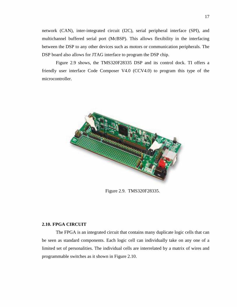
17
network (CAN), inter-integrated circuit (I2C), serial peripheral interface (SPI), and
multichannel buffered serial port (McBSP). This allows flexibility in the interfacing
between the DSP to any other devices such as motors or communication peripherals. The
DSP board also allows for JTAG interface to program the DSP chip.
Figure 2.9 shows, the TMS320F28335 DSP and its control dock. TI offers a
friendly user interface Code Composer V4.0 (CCV4.0) to program this type of the
microcontroller.
Figure 2.9. TMS320F28335.
2.10. FPGA CIRCUIT
The FPGA is an integrated circuit that contains many duplicate logic cells that can
be seen as standard components. Each logic cell can individually take on any one of a
limited set of personalities. The individual cells are interrelated by a matrix of wires and
programmable switches as it shown in Figure 2.10.

18
Figure 2.10. Structure of the FPGA.
A user's design can be implemented by specifying the simple logic function for
each cell and selectively closing the switches in the interconnection matrix. The array of
logic cells and interconnects form a fabric of basic building blocks for logic circuits.
Complex designs are created by combining these basic. The FPGA's functions are
defined by a user's program rather than by the manufacturer of the device.
A typical integrated circuit performs a particular function defined at the time of
manufacture. In contrast, the FPGA's function is defined by a program written by
someone other than the device manufacturer. Depending on the particular device, the
program is either burned in permanently or semi-permanently as part of a board assembly
process, or is loaded from an external memory each time the device is powered up.

19
Figure 2.11 illustrates a typical flow chart for Altera’s FPGA design process,
which has been used in this design.
Figure 2.11. Altera Design Flow Chart [24].
This programmability gives the user access to complex integrated designs without
the high engineering costs associated with application specific integrated circuits.
2.11. POWER SUPPLY BOARD
The power supply is designed in a different printed board (PCB0025) and
attached to the main board through male and female six position power terminals (PES
type and PET type) from SAMTEC Inc. as shown in Figure 2.12 [25], respectively.

20
Figure 2.12. PES and PET Type Connectors [25].
Power modules are used in order to generate seven different voltages as in Table
2.4. Figure 2.13 shows PCB0025 and the next table shows the voltages and the
corresponding parts. The board layout and schematic are attached in appendix A.
Figure 2.13. PCB0025.

21
Table 2.4. Power Modules and Corresponding Voltages.
Voltage Power Module
+1.2V PTH04000W
+3.3V PTH04000W
+3.3V ANA TPS79333DBV
+5.0V PTN78060W
+5.0V ISO. TMH2405S
+15.0V PTN78060H
-15.0V PTN78000A
2.12. PULL-UP RESISTOR CIRCUIT
Pull-up resistors are used for the open collector encoder in order to read the Hall
effect signals. The configuration of this circuit is shown in Figure 2.14.
3.3V
R =1KΩ PU
Open collector switch
Figure 2.14. Pull-up Resistor for Open Collector Configuration.

22
2.13. ERRATA
After testing the board, there were some errors, defects, and considerations for
new version of the board.
The gate signal socket package was inverted in eagle. It has been corrected
in the Lib_DOE_transportation_electrification.lbr in the server.
The DSP package needs to be implemented in the Board as one unit to
minimize the electromagnetic interference (EMI).
R25 has been changed to 2.2kΩ.
R65 and R66 values need to be swapped.
U36 pin 2 and 3 need to be swapped.
U41 pin 1 should be connected to +5V (board defect). Pull-up resistors of
1kΩ need to be added to the Hall effect signals input terminal J21.
Ground terminal needs to be added to J21.
GPIO34 and GPIO 28 need to be swapped.
In PCB0025, pin 1 at U1 and U4 needs to be connected to the ground.
23
3. PULSE WIDTH MODULATOR
3.1. INTRODUCTION
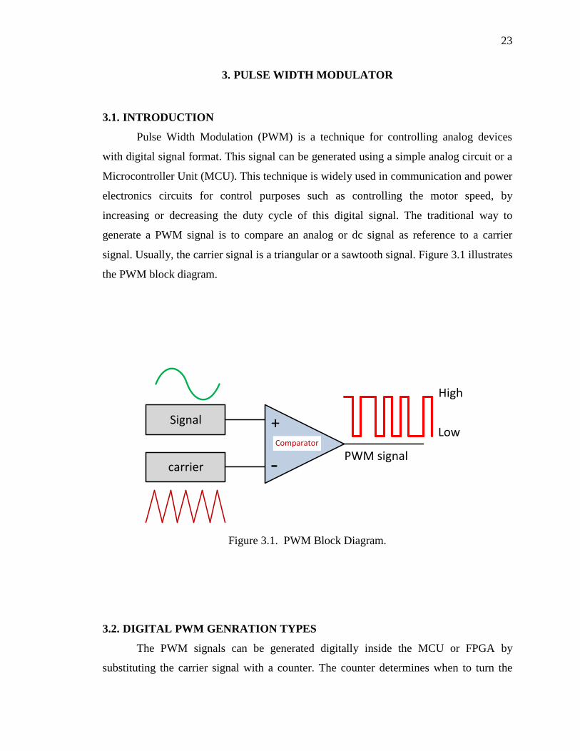
Pulse Width Modulation (PWM) is a technique for controlling analog devices
with digital signal format. This signal can be generated using a simple analog circuit or a
Microcontroller Unit (MCU). This technique is widely used in communication and power
electronics circuits for control purposes such as controlling the motor speed, by
increasing or decreasing the duty cycle of this digital signal. The traditional way to
generate a PWM signal is to compare an analog or dc signal as reference to a carrier
signal. Usually, the carrier signal is a triangular or a sawtooth signal. Figure 3.1 illustrates
the PWM block diagram.
carrier
+Signal
- PWM signal
High
LowComparator
Figure 3.1. PWM Block Diagram.
3.2. DIGITAL PWM GENRATION TYPES
The PWM signals can be generated digitally inside the MCU or FPGA by
substituting the carrier signal with a counter. The counter determines when to turn the

24
PWM signal ON or OFF based on a certain value or reference signal. The counter can be
used at any of the following modes:
Up Mode Counter.
Down Mode Counter.
Up/Down Mode Counter. This results in center-aligned PWM.
3.2.1. Up-Mode Counter. In this mode, the counter starts from zero and
increments until it reach the desired final value. When the counts reach the maximum, the
program will reset the counter to zero and repeat the same procedure again. Figure 3.2
illustrates the up mode counter.
0
1
2
3
45
0
1
2
3
4
0
1
2
3
4
T
5 5
Figure 3.2. Up Mode Counter.
3.2.2. Down-Mode Counter. In this mode, the counter will start to count from
the maximum value and decrements until it reaches zero. When it reaches the zero, the
counter will be reset to the maximum value and repeats the pattern. Figure 3.3 illustrates
the down mode counter.

25
T
54
3
2
1
0
54
3
2
1
0
54
3
2
1
0
Figure 3.3. Down Mode Counter.
3.2.3. Up-Down Mode Counter. In this mode, the counter will start counting
from zero and increments until it reaches the maximum value, then it will start to
decrements until it reaches the zero value and keeps repeating the pattern. Figure 3.4
illustrate the Up-Down counter.
0
1
2
3
45
4
3
2
1
0
1
2
3
45
4
3
2
1
0
T
Figure 3.4. Up-Down Mode Counter.
26
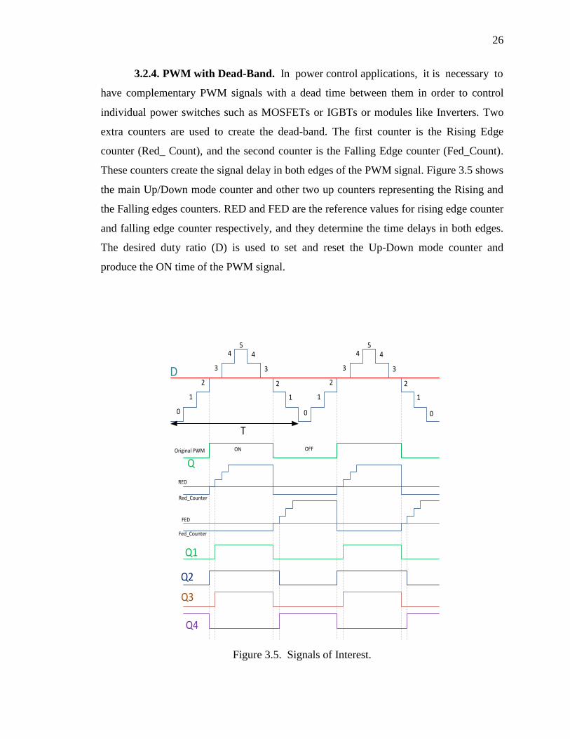
3.2.4. PWM with Dead-Band. In power control applications, it is necessary to
have complementary PWM signals with a dead time between them in order to control
individual power switches such as MOSFETs or IGBTs or modules like Inverters. Two
extra counters are used to create the dead-band. The first counter is the Rising Edge
counter (Red_ Count), and the second counter is the Falling Edge counter (Fed_Count).
These counters create the signal delay in both edges of the PWM signal. Figure 3.5 shows
the main Up/Down mode counter and other two up counters representing the Rising and
the Falling edges counters. RED and FED are the reference values for rising edge counter
and falling edge counter respectively, and they determine the time delays in both edges.
The desired duty ratio (D) is used to set and reset the Up-Down mode counter and
produce the ON time of the PWM signal.
0
1
2
3
45
4
3
2
1
0
1
2
3
45
4
3
2
1
0
T
D
ON OFF
RED
Red_Counter
FED
Fed_Counter
Original PWM
Q1
Q2
Q3
Q4
Q
Figure 3.5. Signals of Interest.

27
Figure 3.6 illustrates the schematic diagram of the up-down counter PWM that
has been implemented using Altera’s Quartus II software. The block diagram composed
of five main blocks and an OR gate.
The first block is the phase locked loop (PLL). The PLL has one input pin
(CLKIN) and two output pins: clock out and LOCKED, a flag indicating that the PLL has
locked to the input. The clock pin is used as clock reference to all blocks while the locked
pin is used to synchronize all blocks in the design. This block is triggered by an external
crystal oscillator (24 MHz) on the module and connected to PLL through pin A12. This
PLL can either increase the frequency in this module up to 48 MHz or decrease it down
to 2.4 MHz in this particular module, in this experiment the clock is chosen to be 24
MHz.
The second block is the PWM constants. This block has no inputs and provides
five constants with different word lengths. The constants are iRed (3 bits), iFed,
iPulseWidth (3 bits), iD (12 bits), and iClkdiv (3 bits). The iRed and iFed is used to
configure the delay in the rising edge and the falling edge respectively. The iPulseWidth
is used to configure the start pulse width in the next block. The iD can be connected to
the PWM block as known data for testing purposes while iClkdiv is connected to ADC
block as clock divider signal in order to slow down the clock inside the block.
The third block generates a start pulse. This block has three inputs and only one
output. The inputs are the clock and locked signals from PLL in block one and the
iPulseWidth signal from the second block. The output is a single pulse used to trigger the
ADC block for the first time through an OR gate. The iPulseWidth signal determines the
length of the start pulse.
The fourth block is the ADC block. This block has five inputs and four outputs.
The inputs are iClk, iStart, iClkdiv, iReset, and iSDO (12 bits). The block starts running
as soon as it receives the iStart pulse from the previous block. This block is a software
written in VHDL for AD7276 [18] to read the serial digital data output through the iSDO
input from the external chip and process it and generate the four output signals which are
the output value (oValOut, 12 bits), serial clock (oSCK), chip select (oLD), and the done
pulse (oDone).

28
Figure 3.6. PWM Schematic Diagram.

29
The last one is the main block which the PWM block. This block has six inputs
which are iStart, iD, iReset, iRed, and iFed. Also, it has thirteen outputs: oQ through
oQ4, oQ_inv through oQ4_inv, oDone, oDone_red, and oDone_fed. The oQx signals are
as shown in Figure 3.5 (with or without inversion). The oDone signals indicate that the
cycle is complete and the next cycle can begin.
The signal flow through these blocks starts with the clock generated from the PLL
to start pulse. The start pulse block generate a single pulse to trigger the ADC block at
(iStart) input to start read the input digital signal oSDO from the real chip. When this
block finishes its process, it generates the serial clock (oSCK), chip select (oLD), output
value (oValOut), and (oDone) which is used to trigger the next block (PWM) at the
(iStart) input to receive the (oValOut) from the ADC through (iD) serial input data
terminal. The PWM block process that data and generate the desired duty ratio. Also, it
uses the constants (iRed) and (iFed) to determine the delay in the rising and falling edges.
After the block finishes the process the generated done pulse is rerouted to the OR gate so
that the process runs continuously.

30
4. PMSM ROTOR POSITION MEASUREMENT
4.1. INTRODUCTION
PMSM control requires the continuous sensing of the rotor position and speed in
order to apply the control algorithms. There are four common methods for measuring the
PMSM rotor position [26].
4.1.1. Optical Encoder. It is the most popular type, which consists of a rotating
disk, a light source, and a photo detector. The disk, which mounted on the drive shaft of
the motor, has coded patterns of opaque and transparent sectors. When the shaft is
rotated, eventually it will rotate the disk and these patterns will interrupt the light emitted
onto the photo-detector and generating a pulse signal output that can determine the rotor
position and the speed. Figure 4.1 [20] displays the optical encoder.
Figure 4.1. Optical Encoder [20].

31
4.1.2. Resolver. The common type is the Transmitter Resolver; it looks like
a small electric motor with a stator and a rotor. The stator consists of three winding
configurations: an exciter and a two two-phase winding (X and Y), in which there is 90°
phase shift. The output of the Resolver is sine and cosine of an angle θ that corresponds
to the shaft position and direction [27]. Figure 4.2 [28] shows the resolver schematic.
Figure 4.2. Resolver Schematic [28].
4.1.3. Full Observer. The Full Observer uses the characteristics of the Back
Electromotive Force and the voltage generated on the windings due to the BEMF. The
polarity of the current induced in the winding due to the BEMF is determined by the
motor rotating direction. The amplitude of the induced current is proportional to the
speed of the rotors. Many manufacturers have implemented this type of observer into
electronic chips.
Figure 4.3 illustrates a diagram of a commonly used Full Observer that uses the
current i, and voltage v, as references through a Proportional Integral (PI) controller
32
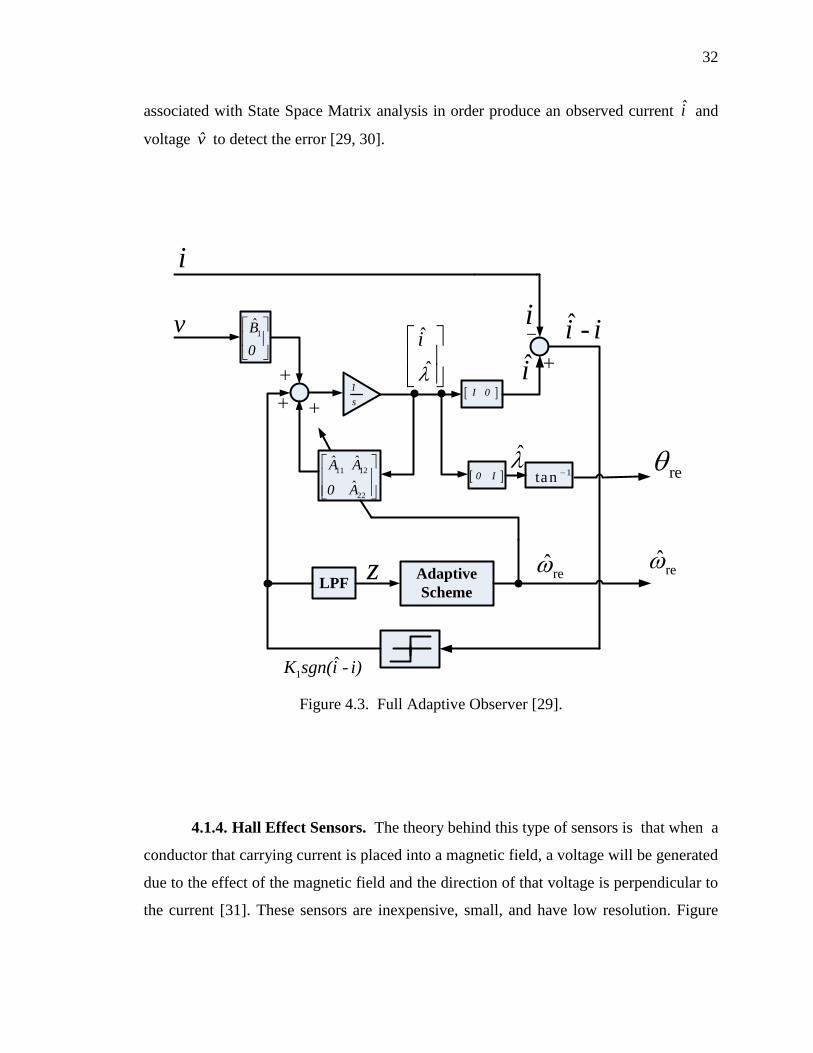
associated with State Space Matrix analysis in order produce an observed current i and
voltage v to detect the error [29, 30].
Adaptive
SchemeLPF
1B
0
1
s
ˆ
ˆ
i
I 0
0 I 1tan 11 12
22
ˆ ˆ
ˆ
A A
0 A
1ˆK sgn(i - i)
z re
i
i
i - i
re
v
re
i
Figure 4.3. Full Adaptive Observer [29].
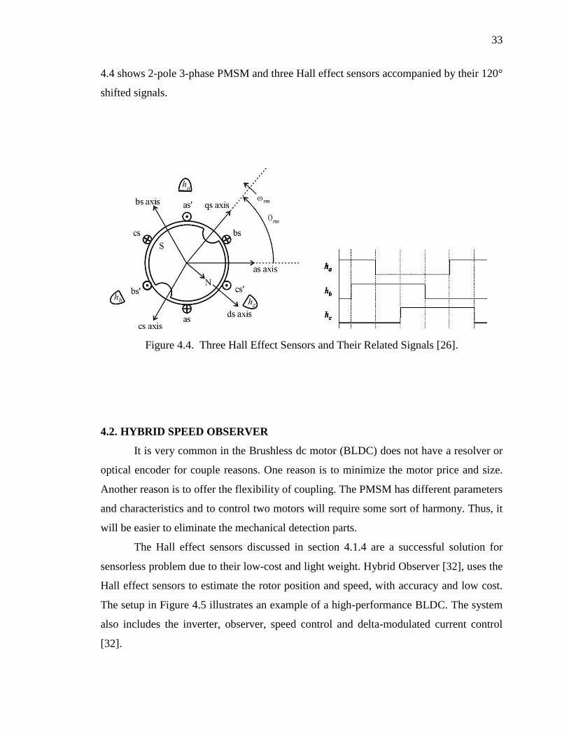
4.1.4. Hall Effect Sensors. The theory behind this type of sensors is that when a
conductor that carrying current is placed into a magnetic field, a voltage will be generated
due to the effect of the magnetic field and the direction of that voltage is perpendicular to
the current [31]. These sensors are inexpensive, small, and have low resolution. Figure
33
4.4 shows 2-pole 3-phase PMSM and three Hall effect sensors accompanied by their 120°
shifted signals.
Figure 4.4. Three Hall Effect Sensors and Their Related Signals [26].
4.2. HYBRID SPEED OBSERVER
It is very common in the Brushless dc motor (BLDC) does not have a resolver or
optical encoder for couple reasons. One reason is to minimize the motor price and size.
Another reason is to offer the flexibility of coupling. The PMSM has different parameters
and characteristics and to control two motors will require some sort of harmony. Thus, it
will be easier to eliminate the mechanical detection parts.
The Hall effect sensors discussed in section 4.1.4 are a successful solution for
sensorless problem due to their low-cost and light weight. Hybrid Observer [32], uses the
Hall effect sensors to estimate the rotor position and speed, with accuracy and low cost.
The setup in Figure 4.5 illustrates an example of a high-performance BLDC. The system
also includes the inverter, observer, speed control and delta-modulated current control
[32].

34
Figure 4.5. High-Performance BLDC [32].
The hybrid observer can be represented by the following differential equation.
rh rhr
rrh rh
cos( ) cos( )0
0sin( ) sin( )
d
dt (17)
If the initial position and the electrical speed are known and equation (17) has a
solution with no error, the sine and cosine of the rotor relevant to the Hall effect sponsors,
then rhsin(θ ) and rhcos(θ ) could be determined using trigonometric identities. Table 4.1
and Figure 5.2 shows the bounding which are maximum and minimum values of rhsin(θ )
and rhcos(θ ) for the current Hall effect sensor states (ha, hb, hc).

35
Table 4.1. Bounding Functions vs. Hall States [32].
Hall State Bounding Functions
ha hb hc maxsin(θh) minsin(θh) maxcos(θh) mincos(θh)
0 0 1 -1/2 -1 0 3 / 2
0 1 0 1 1/2 0 3 / 2
0 1 1 1/2 -1/2 3 / 2 -1
1 0 0 1/2 -1/2 1 3 / 2
1 0 1 -1/2 -1 3 / 2 0
1 1 0 1 1/2 3 / 2 0
The values rhsin(θ ) and rhcos(θ ) can found based on the state transition points.
Table 4.2 shows these values based on the signal states.
Table 4.2. State Transition Points [32].
Sensor Transition ha hb hc rhsin(θ ) rhcos(θ )
ha x 0 1 -1 0
ha x 1 0 1 0
hb 0 x 1 -1/2 3 / 2
hb 1 x 0 1/2 3 / 2
hc 0 1 x 1/2 3 / 2
hc 1 0 x -1/2
x= don’t care

36
Figure 4.6 illustrates how the sine and cosine the angle could be estimated based
on known initial conditions and the bounding conditions of that angle. It also shows the
three different three Hall effect signals are shifted by 120°. At any transition point, the
rotor speed can be estimated based on the time between the transition occurrences,
rhr
ˆt
(18)
The final calculations to implement the hybrid observer to determine the sine and
cosine of the electrical rotor position are
r rh h (19)
Figure 4.6. Hybrid Observer Bounding Functions [26].

37
r rh h rh hsin( ) sin( )cos( ) cos( )sin( ) (20)
r rh h rh hcos( ) cos( )cos( ) sin( )sin( ) (21)
The estimated values of rhsin( ) and rhcos( ) are
r h h h hsin( ) s cos( ) c sin( ) (22)
r h h h hcos( ) c cos( ) s sin( ) (23)
To determine the initial condition for the rotor, the speed is assumed to be zero.
Then hs and hc can be determined from the initial readings of the Hall effect sensor.
Table 4.3 gives these initial conditions. Figure 4.7 illustrates the block diagram of the
hybrid observer.
Table 4.3. Initial Conditions [32].
Initial Hall State Initial Conditions
ha hc hc θh sθh cθh
0 0 1 4π/3 3 / 2 -1/2
0 1 0 2π/3 3 / 2 -1/2
0 1 1 π 0 -1
1 0 0 0 0 1
1 0 1 5π/3 3 / 2 1/2
1 1 0 π/3 3 / 2 1/2

38
All the above equations, initial conditions table, and the transitional table have
been converted into VHDL language in appendix B to estimate the rotor speed and
position. Some of these parameters are treated as signals type while the other signals
treated as variables. A fixed point package [33] is used to add more precision to the
inputs and the estimated outputs. The integration operations are replaced by accumulated
addition operations to estimate the sine and cosine of the electrical angle. The Hall effect
signals have six possible transitions per period. Each transition is used to trigger a
counter to start counting at each transition state and reset itself at the next transition state.
The local estimated rotor speed (lWr) is equal to the length of the period (2π/6) divided
by the time between any two (T1, T2, T3) transitions which is equal to the counter value
(lCount) multiplied by the sampling frequency (Ts) in 34 bits precision. The final value of
the rotor speed has only 12 bit precision due to the lack of precision on the digital to
analog converter (DAC). The error that occurs due to the change of the precision on the
fraction part of the (lWr) is reported and analyzed in chapter five.
Also, the program can estimate the rotor position at any time based on the initial
and the bounding conditions that has been translated into VHDL statements. When the
program starts it looks at initial conditions first and estimates the sine and cosine of θr
and store those values. The sine and cosine θr can be calculated from equations (20) and
(21) respectively.
The new sine and cosine values can be estimated by integrating the equations.
This integration can be replaced by accumulated addition operation as follows,
r,new r,int r r,int SSin( ) Cos( ) Sin( ) T (24)
r,new r,int r r,int SCos( ) Sin( ) Cos( ) T (25)
On the next clock cycle the program will load the new Hall effect states and the
new values of sine and cosine θr will become initial values for the next clock cycle. The

39
program will also check the bounding conditions in Table 4.1 in order not to exceed the
maximum or goes below the maximum and minimum bounding conditions.
Figure 4.7. Hybrid Observer Block Diagram [26].
This speed observer is built in Quartus II software and VHDL language then
simulated at ModelSim, and also implemented and tested in Altera FPGA cyclone II;
appendix B shows the program structure. Figure 4.8 shows the schematic view of the
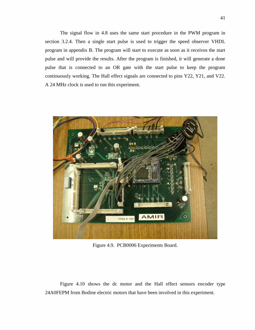
hybrid speed observer. Figure 4.9 displays the FPGA experiments board PCB0006 that
has been used for the implementation of the hybrid speed observer for testing purposes.

40
Figure 4.8. Speed Observer Schematic in VHDL.
41
The signal flow in 4.8 uses the same start procedure in the PWM program in
section 3.2.4. Then a single start pulse is used to trigger the speed observer VHDL
program in appendix B. The program will start to execute as soon as it receives the start
pulse and will provide the results. After the program is finished, it will generate a done
pulse that is connected to an OR gate with the start pulse to keep the program
continuously working. The Hall effect signals are connected to pins Y22, Y21, and V22.
A 24 MHz clock is used to run this experiment.
Figure 4.9. PCB0006 Experiments Board.
Figure 4.10 shows the dc motor and the Hall effect sensors encoder type
24A0FEPM from Bodine electric motors that have been involved in this experiment.

42
Figure 4.10. The Experiment dc Motor.
Table 4.4 illustrates the dc motor parameters and characteristics.
Table 4.4. The Motor Parameters.
Serial number 4440MYEAZ0001
Type 24A0FEPM
Volts 24VDC
F.F 1.0
Amperes 1.2
HP 1/50
INS B8
RPM 2500

43
5. RESULTS AND SYSTEM VALIDATION
5.1. MODELSIM RESULTS
The model of the PWM generator has been tested and developed in ModelSim.
The next figures show the simulation results for three different techniques. Figure 5.1
illustrates the simulation results of up-mode counter.
Figure 5.1. The Simulation Results of the Up-Mode Counter.
Figure 5.2 illustrates the ModelSim simulation results of down-mode counter.
Figure 5.2. The Simulation Results of the Down-Mode Counter.

44
The simulation test is also applied to the Up-Down mode counter and Figure 5.3
displays the simulation results of this type of counter.
Figure 5.3. The Simulation Results of the Up-Down Counter.
Figures 5.4, 5.5, 5.6, 5.7 illustrate the simulation results of the hybrid speed
observer in ModelSim and its related parameters.
Figure 5.4. Screen Shot (1) for Parameters Results of the SO.

45
Figure 5.5. Screen Shot (2) for Parameters Results of the SO.
Figure 5.6. Screen Shot (3) for Parameters Results of the SO.
46
Figure 5.7. Screen Shot (4) for Parameters Results of the SO.
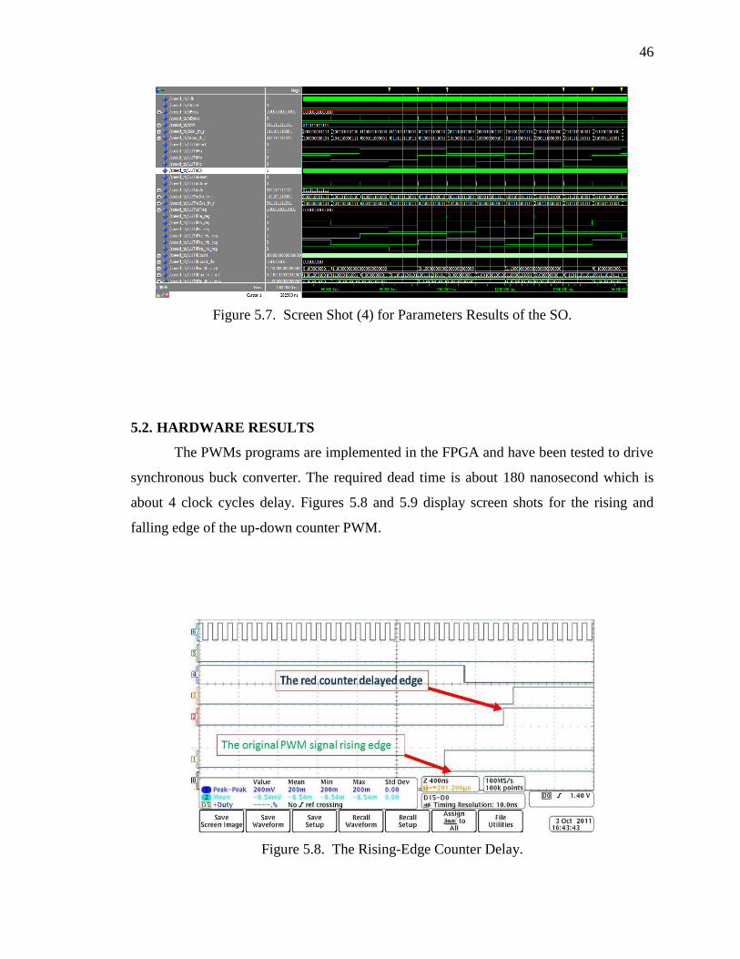
5.2. HARDWARE RESULTS
The PWMs programs are implemented in the FPGA and have been tested to drive
synchronous buck converter. The required dead time is about 180 nanosecond which is
about 4 clock cycles delay. Figures 5.8 and 5.9 display screen shots for the rising and
falling edge of the up-down counter PWM.
Figure 5.8. The Rising-Edge Counter Delay.

47
Figure 5.9. The Falling-Edge of the Fed Counter.
Figure 5.10 shows the Hall effect signals from the dc motor in section 5.2.
Figure 5.10. Hall Effect Signals.
48
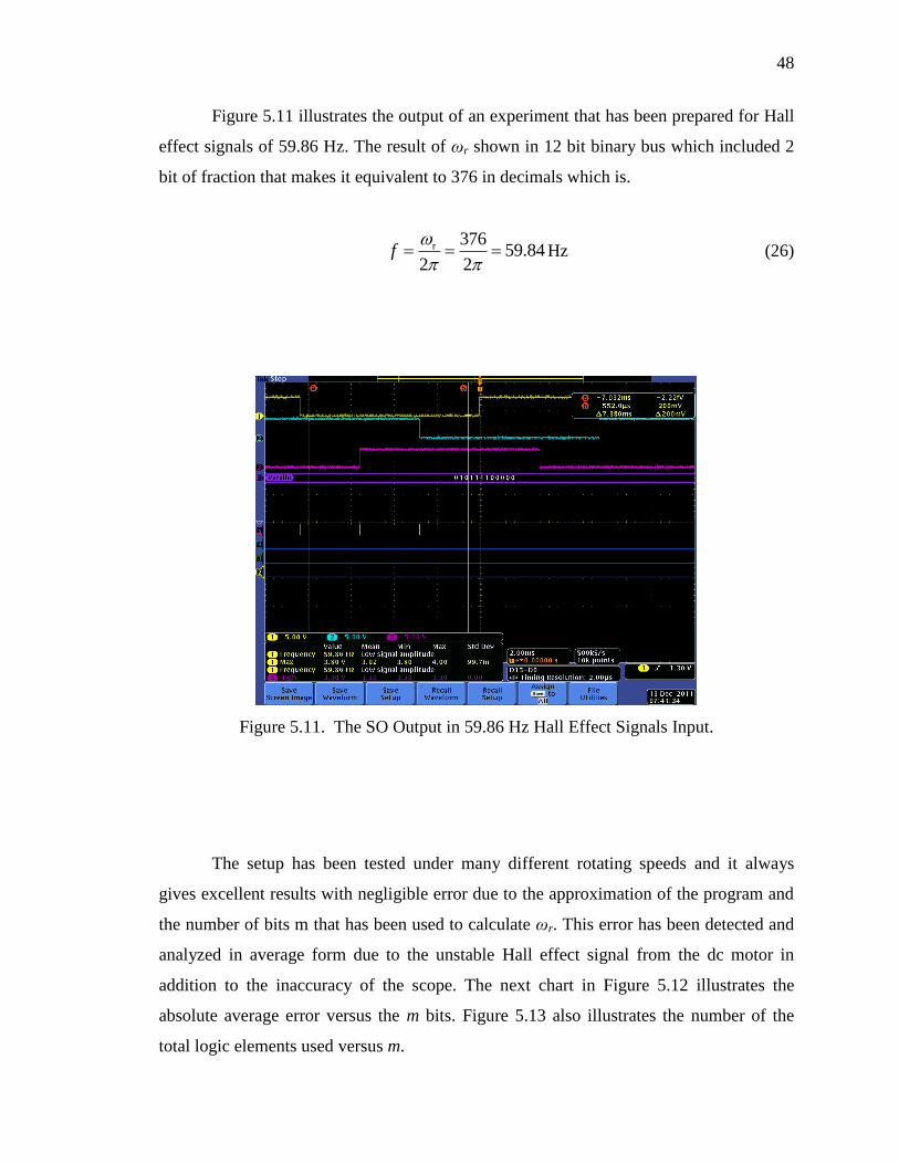
Figure 5.11 illustrates the output of an experiment that has been prepared for Hall
effect signals of 59.86 Hz. The result of ωr shown in 12 bit binary bus which included 2
bit of fraction that makes it equivalent to 376 in decimals which is.
r 37659.84
2 2f
Hz (26)
Figure 5.11. The SO Output in 59.86 Hz Hall Effect Signals Input.
The setup has been tested under many different rotating speeds and it always
gives excellent results with negligible error due to the approximation of the program and
the number of bits m that has been used to calculate ωr. This error has been detected and
analyzed in average form due to the unstable Hall effect signal from the dc motor in
addition to the inaccuracy of the scope. The next chart in Figure 5.12 illustrates the
absolute average error versus the m bits. Figure 5.13 also illustrates the number of the
total logic elements used versus m.

49
Figure 5.12. The Absolute Error vs. m Bits.
Figure 5.13. The Total Logic Elements vs. m Bits.
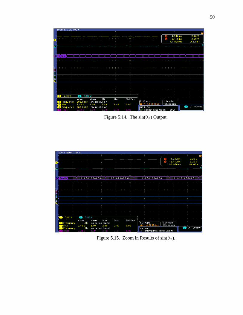
Figures 5.14 and 5.15 illustrate the sin(θrh) output signal from the SO program.
50
Figure 5.14. The sin(θrh) Output.
Figure 5.15. Zoom in Results of sin(θrh).

51
6. CONCLUSION AND FUTURE SCOPE
A signal processing board has been designed to control the PMSM and monitor
the external parameters. This thesis developed the FPGA to generate special signals and
techniques the same as the TI320F28335 does. The PWM signals were tested under
different topologies and conditions. These signals include the dead time capability in
order to be used in synchronous switching devices that require delay time between the
rising and falling edges such as synchronous buck, boost, or buck-boost converters or the
modules like a three phase inverters. The hybrid speed observer method is chosen as the
rotor position and speed detection technique to control the PMSM. This program has
been successfully developed and implemented inside the FPGA and all results are
documented and compared to the microcontroller results. The FPGA implementation
gives high accuracy and better flexibility in the mathematical operations. Also the
resulting error has been analyzed. The system is scalable, so it can control more than one
motor due to the better flexibility of FPGA implementation. The future work would be
applying some other control methods such as all digital phase lock loop (ADPLL), which
is composed of phase and frequency detector, low pass filter (LPF), digital controlled
oscillator (DCO), and a divider. Then a useful comparison can be done to illustrate the
pros and cons of each method.

52
APPENDIX A.
PRINTED CIRCUIT BOARDS DESIGN

53
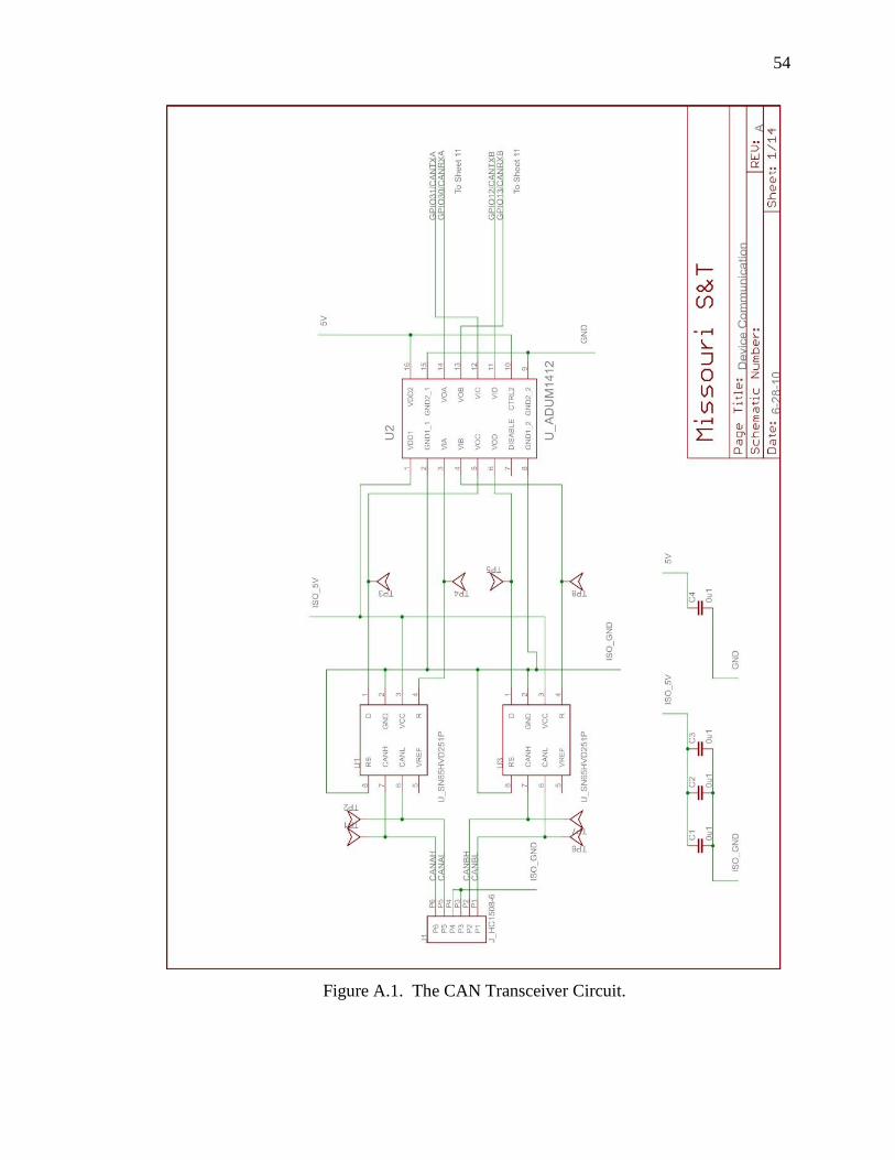
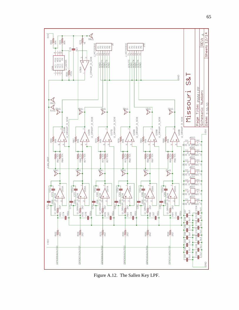
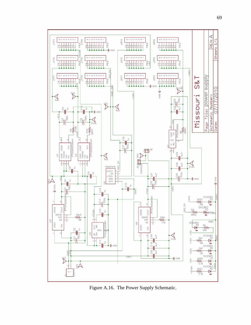
This appendix includes the signal processing and power supply boards schematics
and layouts of the printed circuit boards discussed in Section 2.1 and 2.11 respectively.
The board schematic layout for the signal processing is shown in Figure A.1 through
A.15 and the schematic and layout of the power supply board is shown in Figure A.16
through A.17.
54
Figure A.1. The CAN Transceiver Circuit.

55
Figure A.2. Digital Output Contactors.

56
Figure A.3. The 8-channel AD7329 Serial ADC Circuit.

57
Figure A.4. The ADC AD7276 Circuit.

58
Figure A.5. Level Shifters Circuit.

59
Figure A.6. The FPGA Pin Out.

60
Figure A.7. 0-3V Gain-Offset Circuit.

61
Figure A.8. Differential Input Gain-Offset Circuit.

62
Figure A.9. Digital Inputs Circuit.

63
Figure A.10. Differential Amplifiers Circuit.

64
Figure A.11. The DSP Pin Out.
65
Figure A.12. The Sallen Key LPF.

66
Figure A.13. The Connectors Pin Out.

67
Figure A.14. The Hall effect Signals Level Shitter Sircuit.
68
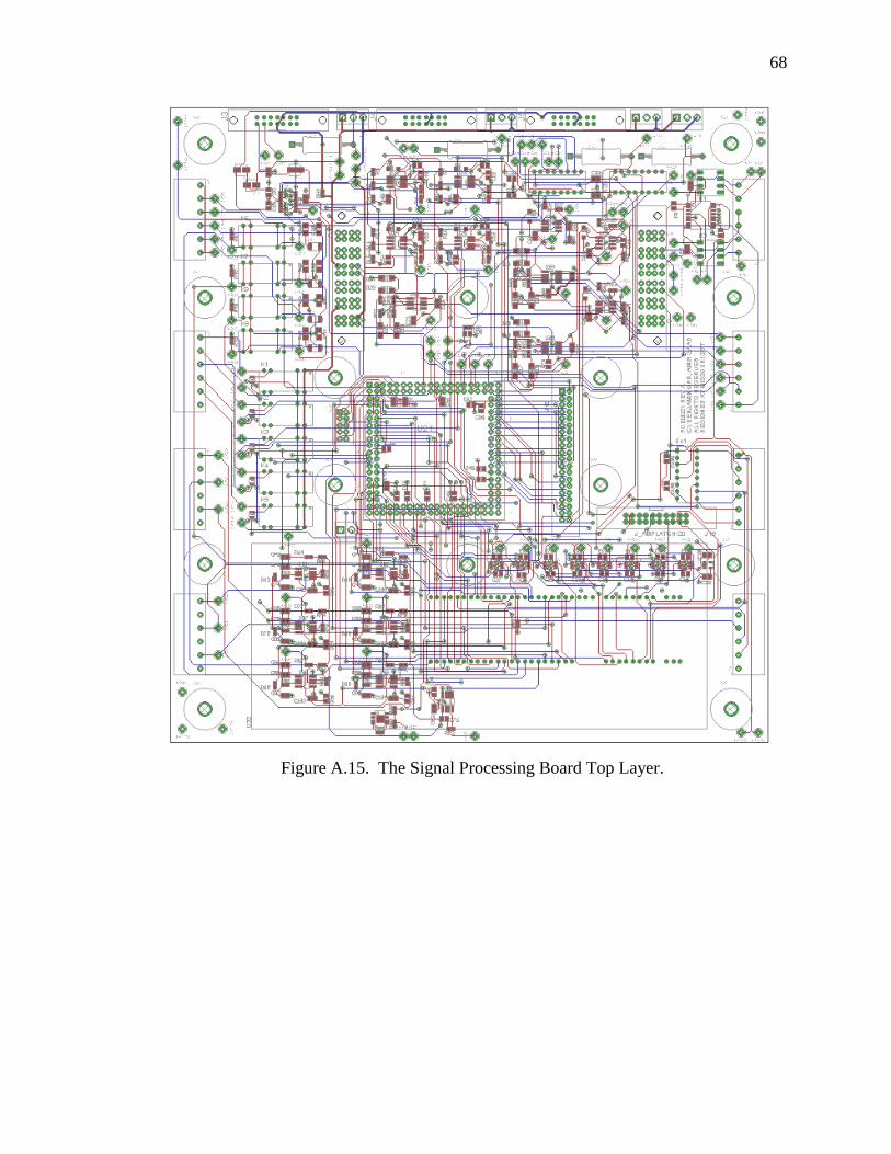
Figure A.15. The Signal Processing Board Top Layer.
69
Figure A.16. The Power Supply Schematic.

70
Figure A.17. The Power Supply Board Top Layer.

71
APPENDIX B.
VHDL CODES OF THE DESIGN

72
This appendix contains the VHDL programs of the up mode, down mode, and up-
down mode PWMs, also it includes the speed observer program. The comments are
denoted by text that starts with double hyphen (--) and green font.

73
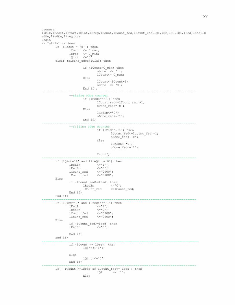
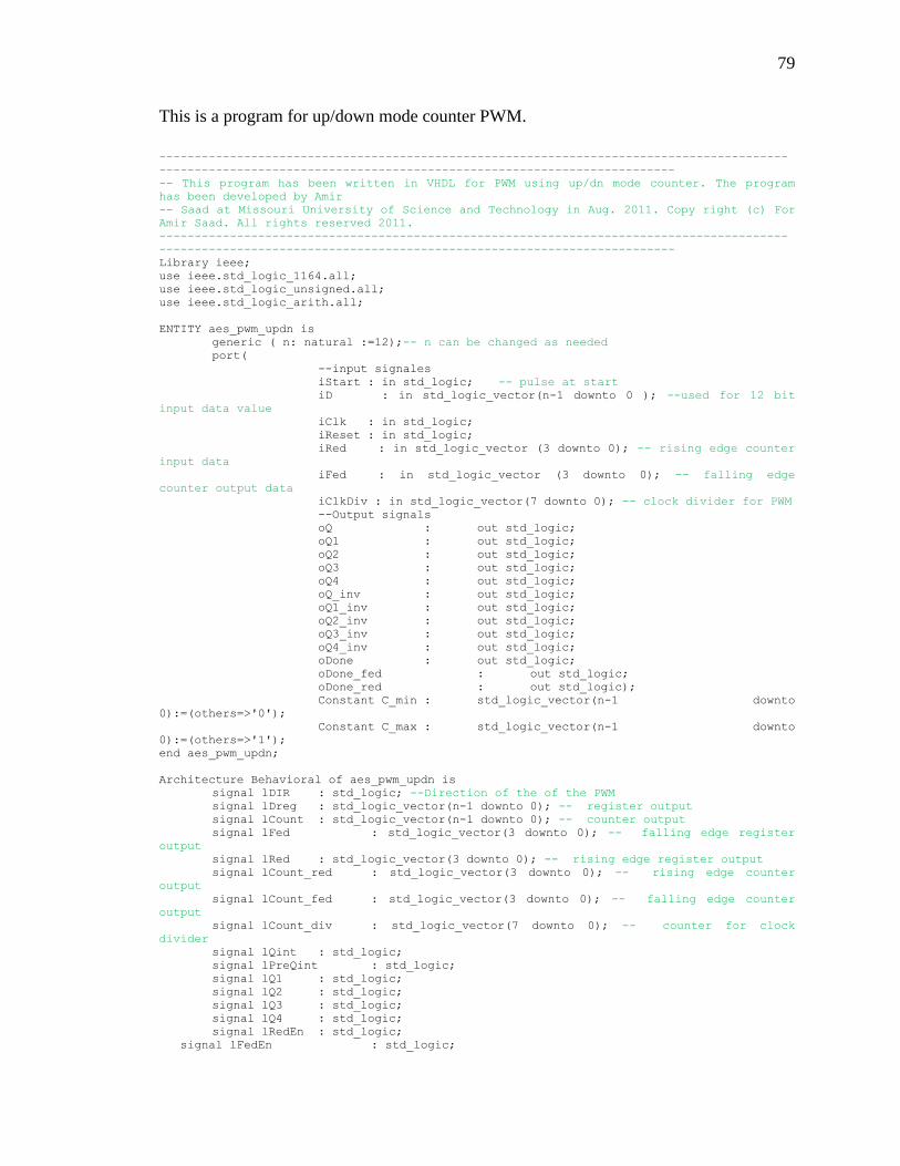
This is a program for up mode counter PWM.
------------------------------------------------------------------------------------------------------------------------------------------------------------------ --This program has been written in VHDL for PWM using up mode counter. The program has been developed by Amir Saad at -- Missouri University of Science and Technology in Aug. 2011 . Copy right (c) For Amir Saad. All rights reserved 2011. ------------------------------------------------------------------------------------------------------------------------------------------------------------------ Library ieee; use ieee.std_logic_1164.all; use ieee.std_logic_unsigned.all; use ieee.std_logic_arith.all; ENTITY aes_pwm_up is generic ( n: natural := 12);-- n can be changed as needed port( --input signales iStart : in std_logic; -- pulse at start iD : in std_logic_vector(n-1 downto 0 ); --used for 12 bit input data value iClk : in std_logic; iReset : in std_logic; iRed : in std_logic_vector (3 downto 0); -- rising edge counter input data iFed : in std_logic_vector (3 downto 0); -- falling edge counter output data --Output signals oQ : out std_logic; oQ1 : out std_logic; oQ2 : out std_logic; oQ3 : out std_logic; oQ4 : out std_logic; oQ_inv : out std_logic; oQ1_inv : out std_logic; oQ2_inv : out std_logic; oQ3_inv : out std_logic; oQ4_inv : out std_logic; oDone : out std_logic; oDone_fed : out std_logic; oDone_red : out std_logic); Constant C_min : std_logic_vector(n-1 downto 0):=(others=>'0'); Constant C_max : std_logic_vector(n-1 downto 0):=(others=>'1'); end aes_pwm_up ; Architecture Behavioral of aes_pwm_up is signal lDreg : std_logic_vector(n-1 downto 0); -- register output signal lCount : std_logic_vector(n-1 downto 0); -- counter output signal lFed : std_logic_vector(3 downto 0); -- falling edge register output signal lRed : std_logic_vector(3 downto 0); -- rising edge register output signal lCount_red : std_logic_vector(3 downto 0); -- rising edge counter output signal lCount_fed : std_logic_vector(3 downto 0); -- falling edge counter output signal lQint : std_logic; signal lPreQint : std_logic; signal lQ1 : std_logic; signal lQ2 : std_logic; signal lQ3 : std_logic; signal lQ4 : std_logic; signal lRedEn : std_logic; signal lFedEn : std_logic; Begin process (iClk,iReset,iStart,lQint,lDreg,lCount,lCount_fed,lCount_red,lQ1,lQ2,lQ3,lQ4,lFed,lRed,lRedEn,lFedEn,lPreQint) Begin -- Initializations if (iReset = '0') then lCount <= C_min; lDreg <= C_min; lFed <= "0000"; lRed <= "0000"; lQint <='0'; lQ1 <='0'; lQ2 <='0'; lQ3 <='0'; lQ4 <='0'; lRedEn <='0'; lFedEn <='0';

74
lCount_red<="0000"; lCount_fed<="0000"; elsif ( rising_edge(iClk)) then if (lCount=C_max) then oDone <= '1'; lCount<= C_min; Else lCount<=lCount+1; oDone <= '0'; End if ; ------------------------------------------------------------------------------------ --rising edge counter if (lRedEn='1') then lCount_red<=lCount_red +1; oDone_red<='0'; Else lRedEn<='0'; oDone_red<='1'; End if; ------------------------------------------------------------------------------------ --falling edge counter if (lFedEn='1') then lCount_fed<=lCount_fed +1; oDone_fed<='0'; Else lFedEn<='0'; oDone_fed<='1'; End if; ------------------------------------------------------------------------------------ if (lQint='1' and lPreQint='0') then lRedEn <='1'; lFedEn <='0'; lCount_red<="0000"; lCount_fed<="0000"; Else if (lCount_red>=lRed) then lRedEn <='0'; lCount_red<=lCount_red; End if; End if; ------------------------------------------------------------------------------------ if (lQint='0' and lPreQint='1') then lFedEn <='1'; lRedEn <='0'; lCount_fed<="0000"; lCount_red<="0000"; Else if (lCount_fed>=lFed) then lFedEn <='0'; End if; End if; ------------------------------------------------------------------------------------- if (lCount >= lDreg) then lQint<='1'; Else lQint <='0'; End if; ------------------------------------------------------------------------------------ if ( lCount >=lDreg or lCount_fed<= lFed ) then lQ1 <= '1'; Else lQ1 <='0';

75
End if; ------------------------------------------------------------------------------------ if ( lCount_red >= lRed ) then lQ2 <= '1'; Else lQ2 <='0'; End if; ------------------------------------------------------------------------------------ lQ3 <= lQ1 and lQ2; ------------------------------------------------------------------------------------ if ( lCount_fed >= lFed) then lQ4 <= '1'; Else lQ4 <='0'; End if; ------------------------------------------------------------------------------------ if ( iStart ='1') then lDreg <= iD; lFed <= iFed; lRed <= iRed; End if; End if; ------------------------------------------------------------------------------------ End process ; oQ <= lQint; oQ1 <= lQ1; oQ2 <= lQ2; oQ3 <= lQ3; oQ4 <= lQ4; oQ_inv <= not (lQint); oQ1_inv <= not (lQ1); oQ2_inv <= not (lQ2); oQ3_inv <= not (lQ3); oQ4_inv <= not (lQ4); End Behavioral ; ----------------------------------------------------------------------------------------------------------------------------------------------------------------------------------------------------------------------------------------------------------------------------------------------------------------------------

76
This is a program for down mode counter PWM.
-----------------------------------------------------------------------------------------
---------------------------------------------------------------------
This program has been written in VHDL for PWM using down mode counter. The program has
been developed by Amir
Saad at Missouri University of Science and Technology in Aug. 2011. Copy right (c) For
Amir Saad. All rights reserved 2011.
----------------------------------------------------------------------------------------
--------------------------------------------------------------------
Library ieee;
use ieee.std_logic_1164.all;
use ieee.std_logic_unsigned.all;
use ieee.std_logic_arith.all;
ENTITY aes_pwm_dn is
generic ( n: natural := 12);-- n can be changed as needed
port(
--input signales
iStart : in std_logic; -- pulse at start
iD : in std_logic_vector(n-1 downto 0 ); --used for 12 bit input
data value
iClk : in std_logic;
iReset : in std_logic;
iRed : in std_logic_vector (3 downto 0); -- rising edge counter
input data
iFed : in std_logic_vector (3 downto 0); -- falling edge
counter output data
--Output signals
oQ : out std_logic;
oQ1 : out std_logic;
oQ2 : out std_logic;
oQ3 : out std_logic;
oQ4 : out std_logic;
oQ_inv : out std_logic;
oQ1_inv : out std_logic;
oQ2_inv : out std_logic;
oQ3_inv : out std_logic;
oQ4_inv : out std_logic;
oDone : out std_logic;
oDone_fed : out std_logic;
oDone_red : out std_logic);
Constant C_min : std_logic_vector(n-1 downto
0):=(others=>'0');
Constant C_max : std_logic_vector(n-1 downto
0):=(others=>'1');
end aes_pwm_dn ;
Architecture Behavioral of aes_pwm_dn is
signal lDreg : std_logic_vector(n-1 downto 0); -- register output
signal lCount : std_logic_vector(n-1 downto 0); -- counter output
signal lFed : std_logic_vector(3 downto 0); -- falling edge register
output
signal lRed : std_logic_vector(3 downto 0); -- rising edge register output
signal lCount_red : std_logic_vector(3 downto 0); -- rising edge counter
output
signal lCount_fed : std_logic_vector(3 downto 0); -- falling edge counter
output
signal lQint : std_logic;
signal lPreQint : std_logic;
signal lQ1 : std_logic;
signal lQ2 : std_logic;
signal lQ3 : std_logic;
signal lQ4 : std_logic;
signal lRedEn : std_logic;
signal lFedEn : std_logic;
Begin
77
process
(iClk,iReset,iStart,lQint,lDreg,lCount,lCount_fed,lCount_red,lQ1,lQ2,lQ3,lQ4,lFed,lRed,lR
edEn,lFedEn,lPreQint)
Begin
-- Initializations
if (iReset = '0' ) then
lCount <= C_max;
lDreg <= C_min;
lQint <='0';
elsif (rising_edge(iClk)) then
if (lCount=C_min) then
oDone <= '1';
lCount<= C_max;
Else
lCount<=lCount-1;
oDone <= '0';
End if ;
------------------------------------------------------------------------------------
--rising edge counter
if (lRedEn='1') then
lCount_red<=lCount_red +1;
oDone_red<='0';
Else
lRedEn<='0';
oDone_red<='1';
End if;
------------------------------------------------------------------------------------
--falling edge counter
if (lFedEn='1') then
lCount_fed<=lCount_fed +1;
oDone_fed<='0';
Else
lFedEn<='0';
oDone_fed<='1';
End if;
------------------------------------------------------------------------------------
if (lQint='1' and lPreQint='0') then
lRedEn <='1';
lFedEn <='0';
lCount_red <="0000";
lCount_fed <="0000";
Else
if (lCount_red>=lRed) then
lRedEn <='0';
lCount_red <=lCount_red;
End if;
End if;
------------------------------------------------------------------------------------
if (lQint='0' and lPreQint='1') then
lFedEn <='1';
lRedEn <='0';
lCount_fed <="0000";
lCount_red <="0000";
Else
if (lCount_fed>=lFed) then
lFedEn <='0';
End if;
End if;
-------------------------------------------------------------------------------------
if (lCount >= lDreg) then
lQint<='1';
Else
lQint <='0';
End if;
------------------------------------------------------------------------------------
if ( lCount >=lDreg or lCount_fed<= lFed ) then
lQ1 <= '1';
Else

78
lQ1 <='0';
End if;
------------------------------------------------------------------------------------
if ( lCount_red >= lRed ) then
lQ2 <= '1';
Else
lQ2 <='0';
End if;
------------------------------------------------------------------------------------
lQ3 <= lQ1 and lQ2;
------------------------------------------------------------------------------------
if ( lCount_fed >= lFed) then
lQ4 <= '1';
Else
lQ4 <='0';
End if;
------------------------------------------------------------------------------------
if ( iStart ='1') then
lDreg <= iD;
lFed <= iFed;
lRed <= iRed;
End if;
End if;
------------------------------------------------------------------------------------
End process ;
oQ <= lQint;
oQ1 <= lQ1;
oQ2 <= lQ2;
oQ3 <= lQ3;
oQ4 <= lQ4;
oQ_inv <= not (lQint);
oQ1_inv <= not (lQ1);
oQ2_inv <= not (lQ2);
oQ3_inv <= not (lQ3);
oQ4_inv <= not (lQ4);
End Behavioral ;
-----------------------------------------------------------------------------------------
79
This is a program for up/down mode counter PWM.
-----------------------------------------------------------------------------------------
-------------------------------------------------------------------------
-- This program has been written in VHDL for PWM using up/dn mode counter. The program
has been developed by Amir
-- Saad at Missouri University of Science and Technology in Aug. 2011. Copy right (c) For
Amir Saad. All rights reserved 2011.
-----------------------------------------------------------------------------------------
-------------------------------------------------------------------------
Library ieee;
use ieee.std_logic_1164.all;
use ieee.std_logic_unsigned.all;
use ieee.std_logic_arith.all;
ENTITY aes_pwm_updn is
generic ( n: natural :=12);-- n can be changed as needed
port(
--input signales
iStart : in std_logic; -- pulse at start
iD : in std_logic_vector(n-1 downto 0 ); --used for 12 bit
input data value
iClk : in std_logic;
iReset : in std_logic;
iRed : in std_logic_vector (3 downto 0); -- rising edge counter
input data
iFed : in std_logic_vector (3 downto 0); -- falling edge
counter output data
iClkDiv : in std_logic_vector(7 downto 0); -- clock divider for PWM
--Output signals
oQ : out std_logic;
oQ1 : out std_logic;
oQ2 : out std_logic;
oQ3 : out std_logic;
oQ4 : out std_logic;
oQ_inv : out std_logic;
oQ1_inv : out std_logic;
oQ2_inv : out std_logic;
oQ3_inv : out std_logic;
oQ4_inv : out std_logic;
oDone : out std_logic;
oDone_fed : out std_logic;
oDone_red : out std_logic);
Constant C_min : std_logic_vector(n-1 downto
0):=(others=>'0');
Constant C_max : std_logic_vector(n-1 downto
0):=(others=>'1');
end aes_pwm_updn;
Architecture Behavioral of aes_pwm_updn is
signal lDIR : std_logic; --Direction of the of the PWM
signal lDreg : std_logic_vector(n-1 downto 0); -- register output
signal lCount : std_logic_vector(n-1 downto 0); -- counter output
signal lFed : std_logic_vector(3 downto 0); -- falling edge register
output
signal lRed : std_logic_vector(3 downto 0); -- rising edge register output
signal lCount_red : std_logic_vector(3 downto 0); -- rising edge counter
output
signal lCount_fed : std_logic_vector(3 downto 0); -- falling edge counter
output
signal lCount_div : std_logic_vector(7 downto 0); -- counter for clock
divider
signal lQint : std_logic;
signal lPreQint : std_logic;
signal lQ1 : std_logic;
signal lQ2 : std_logic;
signal lQ3 : std_logic;
signal lQ4 : std_logic;
signal lRedEn : std_logic;
signal lFedEn : std_logic;

80
Begin
process
(iClk,iReset,iStart,lDIR,lQint,lDreg,lCount,lCount_fed,lCount_red,lQ1,lQ2,lQ3,lQ4,lFed,lR
ed,lRedEn,lFedEn,lPreQint)
Begin
-- Initializations
if (iReset = '0') then
lCount <= C_min;
lDIR <= '0';
lDreg <= C_min;
lFed <= "0000";
lRed <= "0000";
lQint <='0';
lQ1 <='0';
lQ2 <='0';
lQ3 <='0';
lQ4 <='0';
lRedEn <='0';
lFedEn <='0';
lCount_red <="0000";
lCount_fed <="0000";
lCount_div <= "00000000";
elsif ( rising_edge(iClk) ) then
if (lCount_div = iClkDiv) then
lCount_div <= "00000000";
if (lDIR = '1') then
if (lCount= C_max) then
lDIR <= '0';
oDone<= '0';
lCount<=lCount-1;
Else
lCount<=lCount+1;
oDone<= '0';
End if;
Else
if (lCount= C_min) then
lDIR<='1';
oDone<= '1';
lCount<=lCount + 1;
Else
oDone<= '0';
lCount<=lCount - 1;
End if ;
End if ;
Else
lCount_div <= lCount_div + 1;
end if;
lPreQint<=lQint;
------------------------------------------------------------------------------------
--rising edge counter
if (lRedEn='1') then
lCount_red<=lCount_red +1;
oDone_red<='0';
Else
lRedEn<='0';
oDone_red<='1';
End if;
------------------------------------------------------------------------------------
--falling edge counter
if (lFedEn='1') then
lCount_fed<=lCount_fed +1;
oDone_fed<='0';
Else
lFedEn<='0';
oDone_fed<='1';
End if;
------------------------------------------------------------------------------------
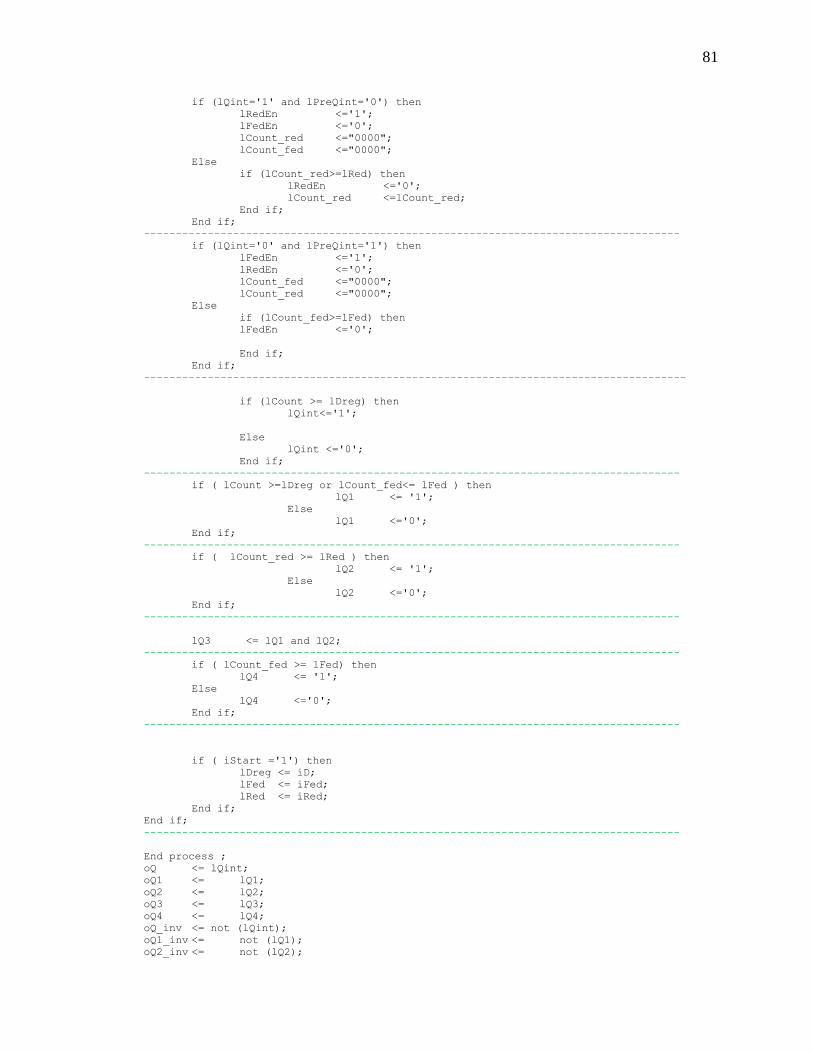
81
if (lQint='1' and lPreQint='0') then
lRedEn <='1';
lFedEn <='0';
lCount_red <="0000";
lCount_fed <="0000";
Else
if (lCount_red>=lRed) then
lRedEn <='0';
lCount_red <=lCount_red;
End if;
End if;
------------------------------------------------------------------------------------
if (lQint='0' and lPreQint='1') then
lFedEn <='1';
lRedEn <='0';
lCount_fed <="0000";
lCount_red <="0000";
Else
if (lCount_fed>=lFed) then
lFedEn <='0';
End if;
End if;
-------------------------------------------------------------------------------------
if (lCount >= lDreg) then
lQint<='1';
Else
lQint <='0';
End if;
------------------------------------------------------------------------------------
if ( lCount >=lDreg or lCount_fed<= lFed ) then
lQ1 <= '1';
Else
lQ1 <='0';
End if;
------------------------------------------------------------------------------------
if ( lCount_red >= lRed ) then
lQ2 <= '1';
Else
lQ2 <='0';
End if;
------------------------------------------------------------------------------------
lQ3 <= lQ1 and lQ2;
------------------------------------------------------------------------------------
if ( lCount_fed >= lFed) then
lQ4 <= '1';
Else
lQ4 <='0';
End if;
------------------------------------------------------------------------------------
if ( iStart ='1') then
lDreg <= iD;
lFed <= iFed;
lRed <= iRed;
End if;
End if;
------------------------------------------------------------------------------------
End process ;
oQ <= lQint;
oQ1 <= lQ1;
oQ2 <= lQ2;
oQ3 <= lQ3;
oQ4 <= lQ4;
oQ_inv <= not (lQint);
oQ1_inv <= not (lQ1);
oQ2_inv <= not (lQ2);

82
oQ3_inv <= not (lQ3);
oQ4_inv <= not (lQ4);
End Behavioral ;

83
This is a program for speed observer.
-----------------------------------------------------------------------------------------
-------------------------------------------------------------------------
-- This program has been written in VHDL for hybrid speed observer to estimate the rotor
positions on continuous basis using the -- information available through the Hall-
effect sensors. The program has been developed by Amir Saad at Missouri University of
-- Science and Technology in Aug. 2011. Copy right (c) For Amir Saad. All rights reserved
2011. --------------------------------------------------
-----------------------------------------------------------------------------------------
-----------------------
Library ieee;
use ieee.std_logic_1164.all;
use ieee.std_logic_unsigned.all;
use ieee.std_logic_arith.all;
library floatfixlib;
use floatfixlib.fixed_pkg.all;
use floatfixlib.float_pkg.all;
ENTITY aes_speed_observer is
generic ( n: natural := 24;-- n&m can be change depending on the precision of
the angles
m: natural := 24;-- the fraction part of Wr
r: natural := 52;-- the precision of Cos phi
s: natural := 5;-- the integer part of the time
x: natural := 32;-- the integer part of Wr
F: natural := 12;
y: natural := 24;-- the number of the bits in the counter
a: real := 0.898794;
b: real := 0.438371;
c: real := 0.0000000417;
d: real := 1.0472;
e: real := 0.1591549431;
z: natural :=8;
q : natural := 12 );
port( --input signals
iStart : in std_logic; -- pulse at start
iHa : in std_logic; -- Hall effect sensor signal
iHb : in std_logic; -- Hall effect sensor signal
iHc : in std_logic; -- Hall effect sensor signal
iClk : in std_logic; -- the clock signal
iReset : in std_logic; -- reset signal
--Output signals
oDone : out std_logic;
oT1 : out std_logic;
oT2 : out std_logic;
oT3 : out std_logic;
oWr : out sfixed(F-1 downto 0); -- pulse done when end
the operation
oSin_th_r : out sfixed(F-1 downto 0); --
oCos_th_r : out sfixed(F-1 downto 0);
oFreq : out sfixed(F-1 downto 0)
);
Constant C_min : std_logic_vector(y-1 downto
0):=(others=>'0');
Constant C_max : std_logic_vector(y-1 downto
0):=(others=>'1');
end aes_speed_observer;
Architecture Behavioral of aes_speed_observer is
signal lCount : std_logic_vector(y-1 downto 0); -- counter output
signal lCount_div : std_logic_vector(7 downto 0); -- counter for
clock divider
signal lSin_th_r_temp : sfixed (0 downto-11);
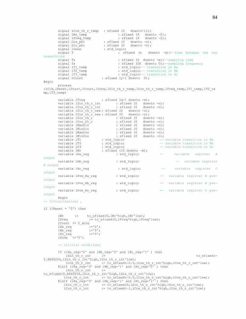
84
signal lCos_th_r_temp : sfixed (0 downto-11);
signal lWr_temp : sfixed (9 downto -2);
signal lFreq_temp : sfixed (9 downto -2);
signal Cos_phi : sfixed (0 downto -n);
signal Sin_phi : sfixed (0 downto -n);
signal lDone : std_logic;
signal T : sfixed (s downto -x);--Time between the two
transitions
signal Ts : sfixed (0 downto -x);--sampling time
signal fs : sfixed (26 downto 0);--sampling frequency
signal lT1_temp : std_logic;-- transition in Ha
signal lT2_temp : std_logic;-- transition in Hb
signal lT3_temp : std_logic;-- transition in Hc
signal tCount : sfixed (y-1 downto 0);
Begin
process
(iClk,iReset,iStart,lCount,lDone,lSin_th_r_temp,lCos_th_r_temp,lFreq_temp,lT1_temp,lT2_te
mp,lT3_temp)
variable lFreq : sfixed (q-1 downto -m);
variable lSin_th_r_int : sfixed (0 downto -n);
variable lCos_th_r_int : sfixed (0 downto -n);
variable lSin_th_r_new : sfixed (0 downto -n);
variable lCos_th_r_new : sfixed (0 downto -n);
variable lSin_th_r : sfixed (0 downto -n);
variable lCos_th_r : sfixed (0 downto -n);
variable lMaxSin : sfixed (0 downto -n);
variable lMinSin : sfixed (0 downto -n);
variable lMaxCos : sfixed (0 downto -n);
variable lMinCos : sfixed (0 downto -n);
variable lT1 : std_logic; -- variable transition in Ha
variable lT2 : std_logic; -- variable transition in Hb
variable lT3 : std_logic; -- variable transition in Hc
variable lWr : sfixed (10 downto -m);
variable lHa_reg : std_logic; -- variable register A
output
variable lHb_reg : std_logic; -- variable register
B output
variable lHc_reg : std_logic; -- variable register C
output
variable lPre_Ha_reg : std_logic; -- variable register A pre-
output
variable lPre_Hb_reg : std_logic; -- variable register B pre-
output
variable lPre_Hc_reg : std_logic; -- variable register C pre-
output
Begin
-- Initializations ,
if (iReset = '0') then
lWr := to_sfixed(0,lWr'high,lWr'low);
lFreq := to_sfixed(0,lFreq'high,lFreq'low);
lCount <= C_min;
lHa_reg :='0';
lHb_reg :='0';
lHc_reg :='0';
lDone <='0';
-- intitial conditions
If (lHa_reg='0' and lHb_reg='0' and lHc_reg='1' ) then
lSin_th_r_int := to_sfixed(-
0.8660254,lSin_th_r_int'high,lSin_th_r_int'low);
lCos_th_r_int := to_sfixed(-0.5,lCos_th_r_int'high,lCos_th_r_int'low);
Elsif (lHa_reg='0' and lHb_reg='1' and lHc_reg='0' ) then
lSin_th_r_int :=
to_sfixed(0.8660254,lSin_th_r_int'high,lSin_th_r_int'low);
lCos_th_r_int := to_sfixed(-0.5,lCos_th_r_int'high,lCos_th_r_int'low);
Elsif (lHa_reg='0' and lHb_reg='1' and lHc_reg='1' ) then
lSin_th_r_int := to_sfixed(0,lSin_th_r_int'high,lSin_th_r_int'low);
lCos_th_r_int := to_sfixed(-1,lCos_th_r_int'high,lCos_th_r_int'low);

85
Elsif (lHa_reg='1' and lHb_reg='0' and lHc_reg='0' ) then
lSin_th_r_int := to_sfixed(0,lSin_th_r_int'high,lSin_th_r_int'low);
lCos_th_r_int := to_sfixed(1,lCos_th_r_int'high,lCos_th_r_int'low);
Elsif (lHa_reg='1' and lHb_reg='0' and lHc_reg='1' ) then
lSin_th_r_int := to_sfixed(-
0.8660254,lSin_th_r_int'high,lSin_th_r_int'low);
lCos_th_r_int := to_sfixed(0.5,lCos_th_r_int'high,lCos_th_r_int'low);
Elsif (lHa_reg='1' and lHb_reg='1' and lHc_reg='0' ) then
lSin_th_r_int :=
to_sfixed(0.8660254,lSin_th_r_int'high,lSin_th_r_int'low);
lCos_th_r_int := to_sfixed(0.5,lCos_th_r_int'high,lCos_th_r_int'low);
Elsif(lHa_reg='1' and lHb_reg='1' and lHc_reg='1' ) then
lSin_th_r_int := to_sfixed(0,lSin_th_r_int'high,lSin_th_r_int'low);
lCos_th_r_int := to_sfixed(0,lCos_th_r_int'high,lCos_th_r_int'low);
End if;
if (lHa_reg='0' and lHb_reg='0' and lHc_reg='1' ) then
lMaxSin := to_sfixed(-0.5,lMaxSin'high,lMaxSin'low);
lMinSin := to_sfixed(-1,lMaxSin'high,lMaxSin'low);
lMaxCos := to_sfixed(0,lMaxCos'high,lMaxCos'low);
lMinCos := to_sfixed(-0.8660254,lMaxCos'high,lMaxCos'low);
Elsif (lHa_reg='0' and lHb_reg='1' and lHc_reg='0' ) then
lMaxSin := to_sfixed(1,lMaxSin'high,lMaxSin'low);
lMinSin := to_sfixed(0.5,lMaxSin'high,lMaxSin'low);
lMaxCos := to_sfixed(0,lMaxCos'high,lMaxCos'low);
lMinCos := to_sfixed(-0.8660254,lMaxCos'high,lMaxCos'low);
Elsif (lHa_reg='0' and lHb_reg='1' and lHc_reg='1' ) then
lMaxSin := to_sfixed(-0.5,lMaxSin'high,lMaxSin'low);
lMaxCos := to_sfixed(-0.8660254,lMaxCos'high,lMaxCos'low);
lMinCos := to_sfixed(-1,lMaxCos'high,lMaxCos'low);
Elsif (lHa_reg='1' and lHb_reg='0' and lHc_reg='0' ) then
lMaxSin := to_sfixed(0.5,lMaxSin'high,lMaxSin'low);
lMinSin := to_sfixed(-0.5,lMaxSin'high,lMaxSin'low);
lMaxCos := to_sfixed(1,lMaxCos'high,lMaxCos'low);
lMinCos := to_sfixed(0.8660254,lMaxCos'high,lMaxCos'low);
Elsif (lHa_reg='1' and lHb_reg='0' and lHc_reg='1' ) then
lMaxSin := to_sfixed(-0.5,lMaxSin'high,lMaxSin'low);
lMinSin := to_sfixed(-1,lMaxSin'high,lMaxSin'low);
lMaxCos := to_sfixed(0.8660254,lMaxCos'high,lMaxCos'low);
lMinCos := to_sfixed(0,lMaxCos'high,lMaxCos'low);
Elsif (lHa_reg='1' and lHb_reg='1' and lHc_reg='0' ) then
lMaxSin := to_sfixed(1,lMaxSin'high,lMaxSin'low);
lMinSin := to_sfixed(0.5,lMaxSin'high,lMaxSin'low);
lMaxCos := to_sfixed(0.8660254,lMaxCos'high,lMaxCos'low);
lMinCos := to_sfixed(0,lMaxCos'high,lMaxCos'low);
End if;
-- Now we can calculate sine and cosine theata_r in the initial conditions mode
Cos_phi <= to_sfixed(a,Cos_phi'High,Cos_phi'Low); -- in this case phi
tken as 26 degrees
Sin_phi <= to_sfixed(b,Sin_phi'High,Sin_phi'Low); -- in this case phi
tken as 26 degrees
Ts <= to_sfixed(c,Ts'High,Ts'Low); -- Sampling time
fs <= to_sfixed(24000000,fs'High,fs'Low); -- Sampling frequency
lSin_th_r :=
resize((lSin_th_r_int*Cos_phi)+(lCos_th_r_int*Sin_phi),lSin_th_r'High,lSin_th_r'Low);
lCos_th_r := resize((lCos_th_r_int*Cos_phi)-
(lSin_th_r_int*Sin_phi),lCos_th_r'High,lCos_th_r'Low);
-- Bounding conditions
elsif ( rising_edge(iClk)) then
Cos_phi <= to_sfixed(a,Cos_phi'High,Cos_phi'Low); -- in this case phi
tken as 26 degrees
Sin_phi <= to_sfixed(b,Sin_phi'High,Sin_phi'Low); -- in this
case phi tken as 26 degrees
Ts <= to_sfixed(c,Ts'High,Ts'Low); -- Sampling time
fs <= to_sfixed(24000000,fs'High,fs'Low); -- Sampling frequency
lHa_reg := iHa;
lHb_reg := iHb;

86
lHc_reg := iHc;
lT1 := (lPre_Ha_reg xor lHa_reg);
lT2 := (lPre_Hb_reg xor lHb_reg);
lT3 := (lPre_Hc_reg xor lHc_reg);
-- Counter to count the time between the transitions
if (lCount= C_max) then
lCount<= C_min;
oDone <= '0';
Else
lCount<=lCount+1;
End if ;
----------------------------------------------------------------------------------
-------------
If (lT1 ='1' or lT2 ='1' or lT3 ='1') then
lCount <= C_min;
lDone <='1';
tCount <= to_sfixed(lCount,tCount'High,tCount'low);
lWr := resize((to_sfixed(1.0472,1,-6)*fs/tCount),lWr'High,lWr'Low);--T is the
time beteen tow transition = lCount*sampling time(Ts)
lCount <= C_min;
lFreq := resize(to_sfixed(e,0,-24)*lWr,lFreq'High,lFreq'Low);-- this is
temparary value for lFreq
Else
lDone <= '0';
End if;
if (lT1 ='1' and lHb_reg='1') then
lSin_th_r_int := to_sfixed(1,lSin_th_r_int'high,lSin_th_r_int'low);
lCos_th_r_int := to_sfixed(0,lCos_th_r_int'high,lCos_th_r_int'low);
Elsif (lT1 ='1' and lHc_reg='1') then
lSin_th_r_int := to_sfixed(-1,lSin_th_r_int'high,lSin_th_r_int'low);
lCos_th_r_int := to_sfixed(0,lCos_th_r_int'high,lCos_th_r_int'low);
Elsif (lT2 ='1' and lHa_reg='1') then
lSin_th_r_int := to_sfixed(0.5,lSin_th_r_int'high,lSin_th_r_int'low);
lCos_th_r_int := to_sfixed(0.8660254,lCos_th_r_int'high,lCos_th_r_int'low);
Elsif (lT2 ='1' and lHc_reg='1') then
lSin_th_r_int := to_sfixed(-0.5,lSin_th_r_int'high,lSin_th_r_int'low);
lCos_th_r_int := to_sfixed(-0.8660254,lCos_th_r_int'high,lCos_th_r_int'low);
Elsif (lT3 ='1' and lHa_reg='1') then
lSin_th_r_int := to_sfixed(-0.5,lSin_th_r_int'high,lSin_th_r_int'low);
lCos_th_r_int := to_sfixed(0.8660254,lCos_th_r_int'high,lCos_th_r_int'low);
Elsif (lT3 ='1' and lHb_reg='1') then
lSin_th_r_int := to_sfixed(0.5,lSin_th_r_int'high,lSin_th_r_int'low);
lCos_th_r_int := to_sfixed(-0.8660254,lCos_th_r_int'high,lCos_th_r_int'low);
End if;
if (lHa_reg='0' and lHb_reg='0' and lHc_reg='1' ) then
lMaxSin := to_sfixed(-0.5,lMaxSin'high,lMaxSin'low);
lMinSin := to_sfixed(-1,lMaxSin'high,lMaxSin'low);
lMaxCos := to_sfixed(0,lMaxCos'high,lMaxCos'low);
lMinCos := to_sfixed(-0.8660254,lMaxCos'high,lMaxCos'low);
Elsif (lHa_reg='0' and lHb_reg='1' and lHc_reg='0' ) then
lMaxSin := to_sfixed(1,lMaxSin'high,lMaxSin'low);
lMinSin := to_sfixed(0.5,lMaxSin'high,lMaxSin'low);
lMaxCos := to_sfixed(0,lMaxCos'high,lMaxCos'low);
lMinCos := to_sfixed(-0.8660254,lMaxCos'high,lMaxCos'low);
Elsif (lHa_reg='0' and lHb_reg='1' and lHc_reg='1' ) then
lMaxSin := to_sfixed(-0.5,lMaxSin'high,lMaxSin'low);
lMaxCos := to_sfixed(-0.8660254,lMaxCos'high,lMaxCos'low);
lMinCos := to_sfixed(-1,lMaxCos'high,lMaxCos'low);
Elsif (lHa_reg='1' and lHb_reg='0' and lHc_reg='0' ) then
lMaxSin := to_sfixed(0.5,lMaxSin'high,lMaxSin'low);
lMinSin := to_sfixed(-0.5,lMaxSin'high,lMaxSin'low);
lMaxCos := to_sfixed(1,lMaxCos'high,lMaxCos'low);
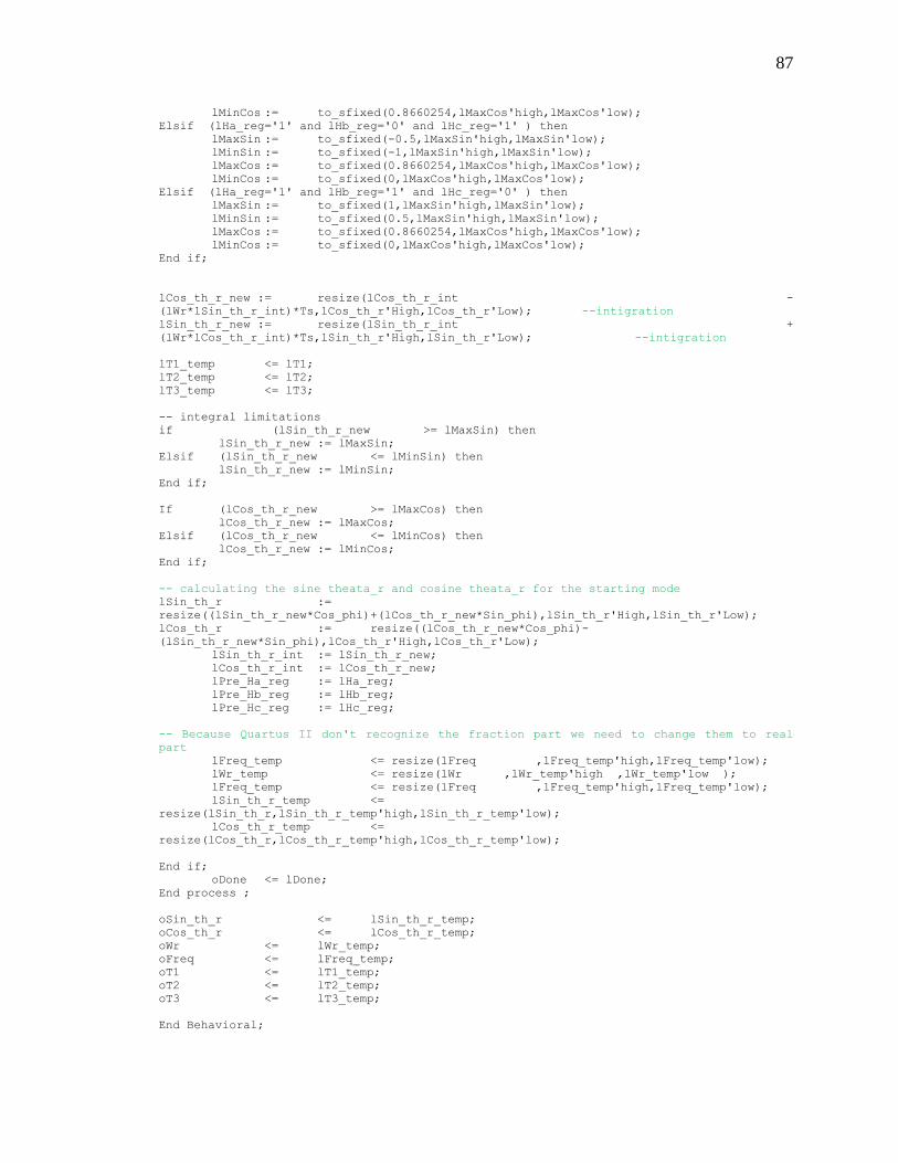
87
lMinCos := to_sfixed(0.8660254,lMaxCos'high,lMaxCos'low);
Elsif (lHa_reg='1' and lHb_reg='0' and lHc_reg='1' ) then
lMaxSin := to_sfixed(-0.5,lMaxSin'high,lMaxSin'low);
lMinSin := to_sfixed(-1,lMaxSin'high,lMaxSin'low);
lMaxCos := to_sfixed(0.8660254,lMaxCos'high,lMaxCos'low);
lMinCos := to_sfixed(0,lMaxCos'high,lMaxCos'low);
Elsif (lHa_reg='1' and lHb_reg='1' and lHc_reg='0' ) then
lMaxSin := to_sfixed(1,lMaxSin'high,lMaxSin'low);
lMinSin := to_sfixed(0.5,lMaxSin'high,lMaxSin'low);
lMaxCos := to_sfixed(0.8660254,lMaxCos'high,lMaxCos'low);
lMinCos := to_sfixed(0,lMaxCos'high,lMaxCos'low);
End if;
lCos_th_r_new := resize(lCos_th_r_int -
(lWr*lSin_th_r_int)*Ts,lCos_th_r'High,lCos_th_r'Low); --intigration
lSin_th_r_new := resize(lSin_th_r_int +
(lWr*lCos_th_r_int)*Ts,lSin_th_r'High,lSin_th_r'Low); --intigration
lT1_temp <= lT1;
lT2_temp <= lT2;
lT3_temp <= lT3;
-- integral limitations
if (lSin_th_r_new >= lMaxSin) then
lSin_th_r_new := lMaxSin;
Elsif (lSin_th_r_new <= lMinSin) then
lSin_th_r_new := lMinSin;
End if;
If (lCos_th_r_new >= lMaxCos) then
lCos_th_r_new := lMaxCos;
Elsif (lCos_th_r_new <= lMinCos) then
lCos_th_r_new := lMinCos;
End if;
-- calculating the sine theata_r and cosine theata_r for the starting mode
lSin_th_r :=
resize((lSin_th_r_new*Cos_phi)+(lCos_th_r_new*Sin_phi),lSin_th_r'High,lSin_th_r'Low);
lCos_th_r := resize((lCos_th_r_new*Cos_phi)-
(lSin_th_r_new*Sin_phi),lCos_th_r'High,lCos_th_r'Low);
lSin_th_r_int := lSin_th_r_new;
lCos_th_r_int := lCos_th_r_new;
lPre_Ha_reg := lHa_reg;
lPre_Hb_reg := lHb_reg;
lPre_Hc_reg := lHc_reg;
-- Because Quartus II don't recognize the fraction part we need to change them to real
part
lFreq_temp <= resize(lFreq ,lFreq_temp'high,lFreq_temp'low);
lWr_temp <= resize(lWr ,lWr_temp'high ,lWr_temp'low );
lFreq_temp <= resize(lFreq ,lFreq_temp'high,lFreq_temp'low);
lSin_th_r_temp <=
resize(lSin_th_r,lSin_th_r_temp'high,lSin_th_r_temp'low);
lCos_th_r_temp <=
resize(lCos_th_r,lCos_th_r_temp'high,lCos_th_r_temp'low);
End if;
oDone <= lDone;
End process ;
oSin_th_r <= lSin_th_r_temp;
oCos_th_r <= lCos_th_r_temp;
oWr <= lWr_temp;
oFreq <= lFreq_temp;
oT1 <= lT1_temp;
oT2 <= lT2_temp;
oT3 <= lT3_temp;
End Behavioral;

88
BIBLIOGRAPHY
[1] A. Raskin and S. Shah, "The Emergence of Hybrid Vehicles," AllianceBernstein.
[2] M. Umeda, H. Itoh, S. Hashimoto, M. Hirata, J. Tsujimura, and S. Kato,
"Permanent magnet motor for EV," in Proc. Power Electronics and Drive
Systems, 1995., Proceedings of 1995 International Conference on, 1995, pp. 792-
796 vol.2.
[3] M. Mekhiche, S. Nichols, J. L. Kirtley, J. Young, D. Boudreau, and R. Jodoin,
"High-speed, high-power density PMSM drive for fuel cell powered HEV
application," in Proc. Electric Machines and Drives Conference, 2001. IEMDC
2001. IEEE International, 2001, pp. 658-663.
[4] M. J. Corley and R. D. Lorenz, "Rotor position and velocity estimation for a
salient-pole permanent magnet synchronous machine at standstill and high
speeds," Industry Applications, IEEE Transactions on, vol. 34, pp. 784-789.
[5] W. Limei and R. D. Lorenz, "Rotor position estimation for permanent magnet
synchronous motor using saliency-tracking self-sensing method," in Proc.
Industry Applications Conference, 2000. Conference Record of the 2000 IEEE,
2000, vol. 1, pp. 445-450 vol.1.
[6] Z.-y. Zhou, Z. Xu, and T.-c. Li, "FPGA implementation of a new hybrid rotor
position estimation scheme based on three symmetrical locked Hall effect position
sensors," in Proc. Power Electronics and Motion Control Conference, 2004.
IPEMC 2004. The 4th International, 2004, vol. 3, pp. 1592-1596 Vol.3.
[7] S. Jiang, J. Liang, Y. Liu, K. Yamazaki, and M. Fujishima, "Modeling and
cosimulation of FPGA-based SVPWM control for PMSM," in Proc. Industrial
Electronics Society, 2005. IECON 2005. 31st Annual Conference of IEEE, 2005,
pp. 6 pp.
[8] X. Z. Qi, Xiaomin; Wang, Changsong; Wang, Xu; and Zhou, Ke, "Rotor position
estimation for a sensorless PMSM using high-frequency signal injection method,"
in Proc. Information, Computing and Telecommunication, 2009. YC-ICT '09.
IEEE Youth Conference on, 2009, pp. 54-57.
[9] B. Zheng, L. Wu, A. Lin, F. Li, C. Yuan, and J. Dang, "Study of a new detection
technology for sensorless PMSM drive with flux linkage observer," in Proc.
Consumer Electronics, Communications and Networks (CECNet), 2011
International Conference on, 2011, pp. 1691-1694.

89
[10] S. Zaim, J. P. Martin, B. Nahid-Mobarakeh, and F. Meibody-Tabar, "High
performance low cost control of a permanent magnet wheel motor using a hall
effect position sensor," in Proc. Vehicle Power and Propulsion Conference
(VPPC), 2011 IEEE, 2011, pp. 1-6.
[11] P. Thiemann, C. Mantala, J. Hordler, et al., "PMSM sensorless rotor position
detection for all speeds by Direct Flux Control," in Proc. Industrial Electronics
(ISIE), 2011 IEEE International Symposium on, 2011, pp. 673-678.
[12] M. a. P. Seilmeier, B., "Modeling of PMSM with multiple saliencies using a
stator-oriented magnetic circuit approach," in Proc. Electric Machines & Drives
Conference (IEMDC), 2011 IEEE International, 2011, pp. 131-136.
[13] K. C. Sam-Young, Choi; Kyeongjin, Lee; and Wootaik, Lee, "An Improved Rotor
Position Estimation With Vector-Tracking Observer in PMSM Drives With Low-
Resolution Hall-Effect Sensors," Industrial Electronics, IEEE Transactions on,
vol. 58, pp. 4078-4086.
[14] Texas Instruments, "Non-Inverting Attenuation with Positive Offset " accessed
on, http://www-k.ext.ti.com/srvs/cgi-bin/webcgi.exe?Company={5761bcd8-11f5-
4e08-84e0-8167176a4ed9},kb=analog,case=obj%2835457%29,new.
[15] D. L. Terrell, OP AMPS Design, Application, and Troubleshooting, Second ed,
1996.
[16] Texas Instruments, "FilterPro™ User's Guide," accessed on,
www.ti.com/lit/an/sbfa001c/sbfa001c.pdf.
[17] Texas Instruments "CMOS Hex Voltage-Level shifter for TTL-to-CMOS or
CMOS-to-TTL Operation," accessed on,
http://www.ti.com/lit/ds/symlink/cd4504b-mil.pdf.
[18] Analog Devices, "AD 7276 8-Bit ADCs in 6-Lead TSOT," accessed on,
http://www.analog.com/static/imported-
files/data_sheets/AD7276_7277_7278.pdf.
[19] Analog Devices, Inc, "Quad-Channel Digital Isolators," accessed on,
http://www.analog.com/static/imported-
files/data_sheets/ADUM1410_1411_1412.pdf.
[20] National Instruments, "Optical Encoder Fundamentals," accessed on,
http://zone.ni.com/devzone/cda/tut/p/id/4672.
[21] TI, "INDUSTRIAL CAN TRANSCEIVER," accessed on,
http://www.ti.com/lit/ds/symlink/sn65hvd251.pdf.

90
[22] Basic Electronics Tutorials "Differential Amplifier," accessed on,
http://www.electronics-tutorials.ws/opamp/opamp_5.html.
[23] TI, "Digital Signal Controllers (DSCs)," accessed on,
http://www.ti.com/lit/ds/symlink/tms320f28335.pdf.
[24] Altera corporation, "FPGA and CPLD Design Flow," accessed on,
http://www.altera.com/products/software/flows/fpga/flo-fpga.html.
[25] Samtec Inc., accessed on,
http://www.samtec.com/ProductInformation/TechnicalSpecifications/Overview.as
px?series=PES.
[26] K. Corzine, "Rotor Position Measurement, EE305," Missouri S&T.
[27] Control Science Inc., "Resolvers as Velocity and Position Encoding Devices,"
accessed on, http://www.controlsciences.com/resolver_application_data.shtml.
[28] Advanced Micro Controls, Inc., "What is the Resolver," accessed on,
http://www.amci.com/tutorials/tutorials-what-is-resolver.asp.
[29] Z. Chen, M. Tomita, S. Doki, and S. Okuma, "New adaptive sliding observers for
position- and velocity-sensorless controls of brushless DC motors," Industrial
Electronics, IEEE Transactions on, vol. 47, pp. 582-591.
[30] T. Furuhashi, S. Sangwongwanich, and S. Okuma, "A position and velocity
sensorless control of brushless DC motors using an adaptive sliding observer," in
Proc. Industrial Electronics Society, 1990. IECON '90., 16th Annual Conference
of IEEE, 1990, pp. 1188-1192 vol.2.
[31] E. Ramsden, Hall-Effect Sensors Theory and Applications: Elsevier Inc.,
Copyright © 2006.
[32] K. A. Corzine and S. D. Sudhoff, "A hybrid observer for high performance
brushless DC motor drives," Energy Conversion, IEEE Transactions on, vol. 11,
pp. 318-323.
[33] vhdl.org, "Fixed point package user’s guide," accessed on,
http://www.eda.org/fphdl/Fixed_ug.pdf.

91
VITA
Amir Saad was born in Omdurman, Sudan. He completed his Bachelor of Science
(B.S.) in Electronic Engineering Technology specialized in Medical Electronics
Engineering from University of Gezira, Wad Medani, Sudan in DEC 1998. He joined his
Master of Science program in Electrical Engineering at Missouri University of Science
and Technology in January 2010 and will receive his Master’s degree in Electrical
Engineering from Missouri University of Science and Technology in May 2012. He has
worked at different companies before making his way back for a higher degree and after
graduation will join Caterpillar Inc. at Advance Components Group.