ladder logic test function software for windows...
TRANSCRIPT


A - 1
• SAFETY PRECAUTIONS •(Always read these instructions before using this equipment.)
Before using this product, please read this manual and the relevant manuals introduced in this manual
carefully and pay full attention to safety to handle the product correctly.
The instructions given in this manual are concerned with this product. For the safety instructions of the
programmable controller system, please read the CPU module user's manual.
In this manual, the safety instructions are ranked as "DANGER" and "CAUTION".
! DANGER
CAUTION!
Indicates that incorrect handling may cause hazardous conditions,resulting in death or severe injury.
Indicates that incorrect handling may cause hazardous conditions, resulting in medium or slight personal injury or physical damage.
Note that the ! CAUTION level may lead to a serious consequence according to the circumstances.
Always follow the instructions of both levels because they are important to personal safety.
Please save this manual to make it accessible when required and always forward it to the end user.
[Cautions Regarding Test Operation]
! DANGER
• The ladder logic test tool (LLT) simulates an actual PLC to debug sequence programs.
However, the execution of a debugged sequence program cannot be guaranteed.
After debugging using the ladder logic test tool (LLT), connect an actual PLC and debug the
sequence program normally before starting actual operation.
Failure to correctly debug a sequence program may result in accidents due to incorrect outputs
of operations.
• The simulated result may differ from actual operation because the ladder logic test tool (LLT)
cannot access I/O units or special function units and do not support some instructions or device
memory.
After debugging using the ladder logic test tool (LLT), connect an actual PLC and debug the
sequence program normally before starting actual operation.
Failure to correctly debug a sequence program may result in accidents due to incorrect outputs
of operations.

A - 2
REVISIONS
The manual number is given on the bottom left of the back cover.
Print Date Manual Number Revision
Feb., 2000 SH(NA)-080064-A First edition
Sep., 2000 SH(NA)-080064-B Partial corrections
A-3, A-6
Partial additions
Section 2.4.6, App22
Nov.2000 SH(NA)-080064-C Partial corrections
5-11
This manual confers no industrial property rights or any rights of any other kind, nor does it confer any patent licenses.Mitsubishi Electric Corporation cannot be held responsible for any problems involving industrial property rights whichmay occur as a result of using the contents noted in this manual.
2000 MITSUBISHI ELECTRIC CORPORATION

A - 3
INTRODUCTION
Thank you for purchasing the Mitsubishi general-purpose MELSEC series sequencer.
Read this manual and make sure you understand the functions and performance of MELSEC series sequencer
thoroughly in advance to ensure correct use.
CONTENTS
Safety Precautions ..........................................................................................................................................A- 1
Revisions .........................................................................................................................................................A- 2
Contents ..........................................................................................................................................................A- 3
About Manuals ................................................................................................................................................A- 6
About the Generic Terms and Abbreviations .................................................................................................A- 7
1. OUTLINE OF LADDER LOGIC TEST TOOL (LLT) 1- 1 to 1- 6
1.1 Features of the Ladder Logic Test Tool (LLT) ....................................................................................... 1- 2
1.2 Differences To Debugging with an Actual PLC Connected................................................................... 1- 5
2. SPECIFICATIONS 2- 1 to 2- 26
2.1 Table of Functions................................................................................................................................... 2- 1
2.2 Function List ............................................................................................................................................ 2- 3
2.3 Devices and Instructions Supported by the Ladder Logic Test Tool (LLT)........................................... 2- 8
2.4 Ladder Logic Test Tool (LLT) Restrictions and Cautions ...................................................................... 2- 9
2.4.1 Restrictions and cautions common to each type of CPU. .............................................................. 2- 9
2.4.2 Restrictions and cautions for the A series CPU functions .............................................................. 2-12
2.4.3 Restrictions and cautions for the QnA series CPU functions ......................................................... 2-14
2.4.4 Restrictions and cautions for the FX series CPU functions............................................................ 2-17
2.4.5 Restrictions and cautions for the Motion controller CPU functions ................................................ 2-19
2.4.6 Restrictions and precautions for the Q series CPU functions ........................................................ 2-20
2.5 Ladder Logic Test Tool (LLT) Safety and Handling Precautions .......................................................... 2-25
3. COMMON OPERATIONS FOR THE LADDER LOGIC TEST TOOL (LLT) 3- 1 to 3- 6
3.1 Procedure from Installation to Debugging.............................................................................................. 3- 1
3.2 GPPW Operations before Debugging.................................................................................................... 3- 3
3.3 Description of the Initial Window Display ............................................................................................... 3- 5
3.4 Ending the Ladder Logic Test Tool (LLT)............................................................................................... 3- 6
4. SIMULATION OF EXTERNAL DEVICE OPERATION --- I/O SYSTEM SETTING FUNCTIONS
4- 1 to 4- 34
4.1 I/O System Setting Operation Procedure............................................................................................... 4- 4
4.2 Start and End of I/O System Setting ...................................................................................................... 4- 5
4.3 Configuration of I/O System Settings Screen ........................................................................................ 4- 6

A - 4
4.4 Setting by Using Timing Chart................................................................................................................ 4- 8
4.5 Operation of Timing Chart Format Input Screen.................................................................................... 4-10
4.5.1 Operation procedure of timing chart format input screen ............................................................... 4-10
4.5.2 Configuration of timing chart format input screen .......................................................................... 4-11
4.5.3 Entering/deleting device................................................................................................................... 4-13
4.5.4 Setting/editing timing........................................................................................................................ 4-15
4.5.5 Setting scan number of timing chart ................................................................................................ 4-21
4.5.6 Other operations............................................................................................................................... 4-22
4.6 Setting by Entering Device Value........................................................................................................... 4-25
4.7 Starting/Stopping the Simulation ............................................................................................................ 4-27
4.8 Other Operations..................................................................................................................................... 4-29
4.8.1 Operating the file .............................................................................................................................. 4-29
4.8.2 Cutting, copying and pasting all settings in the set No. .................................................................. 4-31
4.8.3 Executing monitoring........................................................................................................................ 4-32
4.8.4 Reading I/O system setting file for SW4 of earlier versions ........................................................... 4-34
5. MONITORING DEVICE MEMORY --- MONITOR TEST FUNCTION 5- 1 to 5- 28
5.1 GPPW and Ladder Logic Test Tool (LLT) Monitor Test Functions....................................................... 5- 1
5.2 Operation Procedure of Monitoring Device Memory ............................................................................. 5- 2
5.3 Starting/Ending Monitoring Device Memory........................................................................................... 5- 3
5.4 Monitoring/Testing the Device Memory.................................................................................................. 5- 4
5.4.1 Selecting the devices for monitoring................................................................................................ 5- 4
5.4.2 Stopping and restarting the device memory monitor ...................................................................... 5- 6
5.4.3 Changing the monitor communications interval .............................................................................. 5- 7
5.4.4 Changing the device memory monitor format ................................................................................. 5- 8
5.4.5 Opening the new window................................................................................................................. 5- 9
5.4.6 Running the device test.................................................................................................................... 5-10
5.5 Using Timing Chart ................................................................................................................................. 5-12
5.5.1 Operation procedure of timing chart ................................................................................................ 5-12
5.5.2 Starting/exiting timing chart.............................................................................................................. 5-13
5.5.3 Using timing chart............................................................................................................................. 5-14
5.5.4 Entering/deleting device to be monitored........................................................................................ 5-17
5.5.5 Starting/stopping monitoring ............................................................................................................ 5-20
5.5.6 Operating file .................................................................................................................................... 5-21
5.5.7 Setting sampling period.................................................................................................................... 5-23
5.5.8 Other operations............................................................................................................................... 5-24
5.5.9 Usable devices in the timing chart................................................................................................... 5-27
6. SAVING AND READING THE DEVICE AND BUFFER MEMORIES --- TOOL FUNCTIONS 6- 1 to 6- 6
6.1 Saving the Device and Buffer Memories................................................................................................ 6- 1
6.2 Reading Saved Device Memory or Buffer Memory Data ...................................................................... 6- 3
7. EXAMPLES OF LADDER LOGIC TEST TOOL (LLT) APPLICATIONS 7- 1 to 7- 16
7.1 Debugging Using GPPW Step Execution Function............................................................................... 7- 4
7.2 Using Timing Chart Display for Debugging............................................................................................ 7- 6
7.3 Using I/O System Settings for Debugging.............................................................................................. 7-10

A - 5
8. TROUBLESHOOTING 8- 1 to 8- 8
8.1 Error Messages Displayed on the LED Indicators................................................................................. 8- 1
APPENDICES Appendix- 1 to Appendix- 46
Appendix 1 List of Supported Devices ............................................................................................Appendix- 1
Appendix 1.1 The A series CPU function ladder logic test tool (LLT) ........................................Appendix- 1
Appendix 1.2 The QnA series CPU function ladder logic test tool (LLT) ...................................Appendix- 4
Appendix 1.3 FX series CPU function ladder logic test tool (LLT)..............................................Appendix-10
Appendix 1.4 Ladder logic test tool (LLT) for Q series CPU (A mode) functions.......................Appendix-24
Appendix 1.5 Ladder logic test tool (LLT) for Q series CPU (Q mode) functions ......................Appendix-24
Appendix 2 List of Supported Instruction.........................................................................................Appendix-29
Appendix 2.1 A series CPU function ladder logic test tool (LLT)................................................Appendix-29
Appendix 2.2 QnA series function ladder logic test tool (LLT)....................................................Appendix-31
Appendix 2.3 FX series function ladder logic test tool (LLT) ......................................................Appendix-33
Appendix 2.4 Ladder logic test tool (LLT) for Q series CPU (A mode) functions.......................Appendix-38
Appendix 2.5 Ladder logic test tool (LLT) for Q series CPU (Q mode) functions ......................Appendix-38
Appendix 3 List of Devices Usable with the I/O System Settings...................................................Appendix-40
Appendix 3.1 Condition area........................................................................................................Appendix-40
Appendix 3.2 Simulation device area ..........................................................................................Appendix-42
INDEX Index- 1 to Index- 2
A - 6
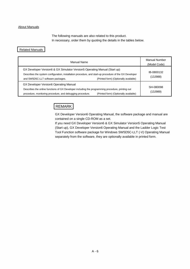
About Manuals
The following manuals are also related to this product.
In necessary, order them by quoting the details in the tables below.
Related Manuals
Manual NameManual Number
(Model Code)
GX Developer Version6 & GX Simulator Version5 Operating Manual (Start up)
Describes the system configuration, installation procedure, and start-up procedure of the GX Developer
and SW5D5C-LLT software packages. (Printed form) (Optionally available)
IB-0800132
(13J988)
GX Developer Version6 Operating Manual
Describes the online functions of GX Developer including the programming procedure, printing out
procedure, monitoring procedure, and debugging procedure. (Printed form) (Optionally available)
SH-080098
(13J989)
REMARK
GX Developer Version6 Operating Manual, the software package and manual are
contained on a single CD-ROM as a set.
If you need GX Developer Version6 & GX Simulator Version5 Operating Manual
(Start up), GX Developer Version6 Operating Manual and the Ladder Logic Test
Tool Function software package for Windows SW5D5C-LLT (-V) Operating Manual
separately from the software, they are optionally available in printed form.

A - 7
About the Generic Terms and Abbreviations
Unless otherwise specified, the table below defines the abbreviations and terminology
of the ladder logic test tool software package of model SW5D5C-LLT-E used in this
manual.
Generic Term/Abbreviation Description
Ladder logic test tool (LLT) Abbreviation for "SW5D5C-LLT-E ladder logic test tool functions software package"GPPW Abbreviation for "SW D5C-GPPW-E GPP function software package"
Windows 95 Abbreviation for "Microsoft Windows 95 (English version)"
Windows 98 Abbreviation for "Microsoft Windows 98 (English version)"
Windows NT 4.0 Abbreviation for "Microsoft Windows NT Workstation 4.0 (English version)"
Debug Locating and correcting errors in a sequence program to create a correct program.
Device memoryAreas to store device data in the ladder logic test tool (LLT), including inputs (X), outputs(Y), relays (M), timers (T), data registers (D), etc.
Monitor Monitoring to determine the ON/OFF status of bit devices or the PV of word devices.
SimulationsTest execution of a program on a personal computer with the ladder logic test tool (LLT)installed, instead of execution in an actual PLC.
Timing chartFunctions to visually confirm ON/OFF status of a bit device or the change in value of aword device.
WDT errorAn error issued when a sequence program is written in such a way that it runs an infiniteloop.
Pseudo-sequence programIndicates a sequence program created by the ladder logic test tool (LLT) to realize thesettings of I/O System Settings.
A series CPUA0J2H, A1FX, A1S (S1), A1SJ, A1SH, A1SJH, A1N, A2C, A2CJ, A2N (S1), A2S (S1),A2SH (S1), A3N, A2A (S1), A3A, A2U (S1), A2US (S1), A2USH-S1, A3U, A4U, CPUboard (A80BD-A2USH-S1)
QnA series CPU Q2A, Q2AS (H), Q2AS1, Q2AS (H) S1, Q3A, Q4A, Q4AR
FX series CPU FX0(S), FX0N, FX1, FX2(C), FX1S, FX1N, FX2N (C)
Motion controller CPU A171SH, A172SH, A173UH (S1), A273UH (S3)
Q series CPU Generic term for Q series CPU (A mode) and Q series CPU (Q mode).
Q series CPU (A mode) Q02-A, Q02H-A, Q06H-A
Q series CPU (Q mode) Q02, Q02H, Q06H, Q12H, Q25H
Microsoft Windows and Microsoft Windows NT are trademarks of Microsoft Corporation U.S.A.
Other names of companies and products are also trademarks or registered trademarks of companies.

A - 8
MEMO

1 - 1
MELSEC1. OUTLINE OF LADDER LOGIC TEST TOOL (LLT)
11. OUTLINE OF LADDER LOGIC TEST TOOL (LLT)
This operating manual describes the functions and operation of the
SW5D5C-LLT-E ladder logic test tool functions software package.
The SW5D5C-LLT-E ladder logic test tool functions software package (hereafter
"ladder logic test tool (LLT)") is a software package which runs under Windows 95/98/
NT4.0.
Offline debugging is possible by adding the ladder logic test tool (LLT) to a computer in
which the SW D5C-GPPW- E/SW D5F-GPPW-E GPP function software package
(hereafter "GPPW") is installed. The offline debugging functions
include the device monitor test and simulated operation of external device I/Os.
As the ladder logic test tool (LLT) allow sequence programs to be developed and
debugged on a single computer, checking a modified program is quick and easy.
GPPW must be installed before these functions can be used.
GPPW Ladder Logic Test Tool (LLT)
Device monitor test, simulated operation of machine side I/Os, etc. are possible.
Connection of PLCis not necessary.
Install
A sequence program created with GPPW can be debugged by writing it to the ladder
logic test tool (LLT).
The sequence program is automatically written to the ladder logic test tool (LLT) when
the ladder logic test tool (LLT) are started up.
See the following manuals for information on operations not covered in this manual:
GPP Function software for Windows SW5D5C-GPPW-E Ladder Logic Test
Functions software SW5D5C-LLT-E Operating Manual (Start up)
................................................................................................................. IB-0800093
GPP Function software for Windows
SW5D5C-GPPW-E
Operating Manual.................................................................................SH-080062
1 - 2
MELSEC1. OUTLINE OF LADDER LOGIC TEST TOOL (LLT)
1.1 Features of the Ladder Logic Test Tool (LLT)
The main features of the ladder logic test tool (LLT) are described below.
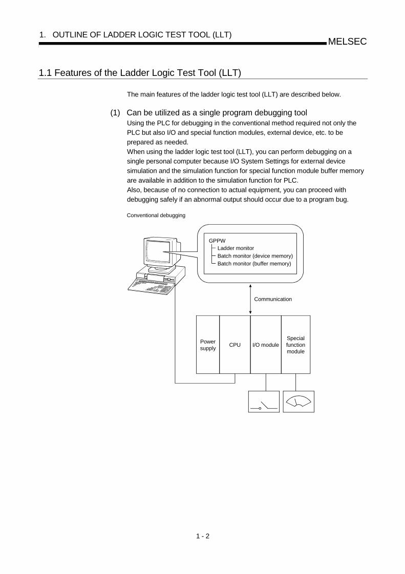
(1) Can be utilized as a single program debugging toolUsing the PLC for debugging in the conventional method required not only the
PLC but also I/O and special function modules, external device, etc. to be
prepared as needed.
When using the ladder logic test tool (LLT), you can perform debugging on a
single personal computer because I/O System Settings for external device
simulation and the simulation function for special function module buffer memory
are available in addition to the simulation function for PLC.
Also, because of no connection to actual equipment, you can proceed with
debugging safely if an abnormal output should occur due to a program bug.
GPPW
Communication
Conventional debugging
Batch monitor (device memory)
Batch monitor (buffer memory)
Ladder monitor
Powersupply
CPU I/O moduleSpecialfunctionmodule

1 - 3
MELSEC1. OUTLINE OF LADDER LOGIC TEST TOOL (LLT)
1) ... Key switch, indicator display function2) ... Function to simulate CPU operation3) ... Function to simulate CPU device memory4) ... Function to simulate the buffer memory area of a special function module5) ... Function to batch-monitor device memory values6) ... Function to display device memory changes in a chart form7) ... Function to simulate I/O operation of external device8) ... Function to save/read device memory or buffer memory data to/from a file
Debugging using ladder logic test tool (LLT)
GPPW
Ladder monitor
Batch monitor (device memory)
Batch monitor (buffer memory)
1) Basic screen
2) CPU simulation function
3) Device memory simulation function
4) Buffer memory simulation function
5) Device batch monitor 6) Timing chart 7) I/O system settings 8) Tool function
LLT
Communication

1 - 4
MELSEC1. OUTLINE OF LADDER LOGIC TEST TOOL (LLT)
(2) Comparison between PLC and ladder logic test tool (LLT)There are the following differences between connection with a PLC and use of
the ladder logic test tool (LLT).
An AnAAnU
Q (A mode)FX QnACPU Q (Q mode) Refer To
Device range 1 1 1 8 8Appendix-
1
Instruction
(common)2 2 2 6 9 9
Appendix-
29
Instruction
(dedicated) 3 3
Appendix-
30
Parameter 4 4 4 7 10 10 2-11
Network
parameter2-11
Special function
module5 5 5 5 5 5
: Supported : Unsupported : Irrelevant
1: Device I is not supported.
2: Output instructions, program branch instructions, data processing instructions, display instructions and
other instructions include unsupported instructions.
3: Structured program instructions, I/O operation instructions, character string processing instructions,
clock instructions, data link instructions and special module instructions include unsupported
instructions.
4: Memory capacity setting, PLC RAS setting, PLC system setting and device setting include
unsupported items.
5: Only the buffer memory area is supported. The size of the buffer memory area is fixed to 16K points.
The QCPU (Q mode) is fixed to 64K points.
6: Program flow instructions, high-speed processing instructions, convenient instructions, external device
instructions, positioning instructions and clock instructions include unsupported instructions.
7: Memory capacity setting, device setting, PLC name setting, PLC system setting (1) and PLC system
setting (2) include unsupported items.
8: Devices S, Jn\X, Jn\Y, Jn\B, Jn\SB, Jn\W, Jn\SW, I, BL and TR are unsupported.
9: Output instructions, program execution instructions, I/O refresh instructions, other convenient
instructions, data processing instructions, structured instructions, display instructions, debugging,
diagnostic instructions, character string processing instructions, special function instructions, data
control instructions, clock instructions, peripheral device instructions and other instructions include
unsupported instructions.
10: PLC name setting, PLC system setting, PLC file setting, PLC RAS setting, device setting, boot file
setting and SFC setting include unsupported items.

1 - 5
MELSEC1. OUTLINE OF LADDER LOGIC TEST TOOL (LLT)
1.2 Differences To Debugging with an Actual PLC Connected
The specifications for debugging using the ladder logic test tool (LLT) differ from those
for debugging with an actual PLC connected.
The main differences between debugging using the ladder logic test tool (LLT) and
debugging with an actual PLC connected are shown below.
See Section 2.4 for details.
Item NameDebugging with an Actual PLC
ConnectedDebugging with Ladder Logic Test Tool (LLT)
Applicable
CPU
Step execution,
skip execution,
partial execution
Not supported by FX series CPU
functions
Debugging using step execution, skip execution, and
partial execution makes debugging operation more
efficient.
FXCPU
Device range
check
Operation continues even if the
indirect designation by the index
register exceeds the device range.
"OPERATION ERROR" occurs when the device range
determined by CPU type or parameters is exceeded.
(For the device range for a specific CPU type, refer to
Appendix 1.)
ACPU
QnACPU
FXCPU
Motion
controller
CPU
QCPU
Real number range
check
Dedicated instructions to handle
real numbers allow operation to
continue when an illegal value
occurs which cannot be evaluated
as a real number.
Real number range checks are conducted rigorously.
"OPERATION ERROR" is displayed if a value cannot be
evaluated as a real number.
ACPU
QnACPU
Motion
controller
CPU
QCPU
Number range
check
Value 0 is given as a result of "0
divided by 0" by DIV instruction,
floating point division, of the A
series PLC.
No error occurs.
The rigorous number range check can detect an illegal 0
denominator and "OPERATION ERROR" is generated if
0 ÷ 0 is executed.
ACPU
Motion
controller
CPU
QCPU
(A mode)
Illegal instruction in
a dedicated
instruction
The illegal instruction is ignored and
operation continues.
The illegal instruction is checked and "INSTRCT CODE
ERR." is displayed. Dedicated instructions must be
described as blocks.
(Example of illegal ladder)
������������������������������������������������������������������������������������������������������������������������������������������������������������������������������������������
RADLEDA
D200LEDC
K120DM0V
LEDR
D500
LEDC D210
END
Illegalinstruction
M9036
ACPU
Motion
controller
CPU
QCPU
(A mode)

1 - 6
MELSEC1. OUTLINE OF LADDER LOGIC TEST TOOL (LLT)
Item NameDebugging with an Actual PLC
Connected
Debugging with Ladder Logic Test
Tool (LLT)
Applicable
CPU
Time concept Actual time As per constant scan setting.
ACPU
QnACPU
FXCPU
Motion
controller
CPU
QCPU
Supported
instructionsAll instructions can be used.
Since data refresh instructions, PID control instructions
(QnA series, FX series CPUs), etc. cannot be used, they
are processed as NOPs.
(Refer to Appendix-2 for supported instructions.)
ACPU
QnACPU
FXCPU
Motion
controller
CPU
QCPU
Operating CPU
typeAccording to CPU type used.
Operates as A4UCPU when an A series CPU is
selected, Q4ACPU when QnA series CPU is selected,
FXCPU when FX series CPU is selected, or A4UCPU
when motion controller CPU is selected.
ACPU
QnACPU
FXCPU
Motion
controller
CPU
QCPU
Special function
module
(special block)
Supported
Not supported.
Only the buffer memory area of a special function
module (special block) is supported.
ACPU
QnACPU
FXCPU
Motion
controller
CPU
QCPU
(A-mode)
I/O module Supported Not supported
ACPU
QnACPU
FXCPU
Motion
controller
CPU
QCPU
Network Supported Not supported
ACPU
QnACPU
FXCPU
Motion
controller
CPU
QCPU
Memory cassette
capacity
An error occurs in GPPW if data
exceeding the memory cassette
capacity is written to the PLC.
No error occurs and normal operation continues if data
exceeding the memory cassette capacity is written to
the PLC.
ACPU
QnACPU
Motion
controller
CPU
QCPU
Intelligent function
module (intelligent
parameters)
SupportedOnly the initial setting, automatic refresh setting and
buffer memory area are supported.
QCPU
(Q mode)

2 - 1
MELSEC2. SPECIFICATIONS
2
2. SPECIFICATIONS
2.1 Table of Functions
The functions supported by the ladder logic test tool (LLT) are shown below.
The functions supported by the ladder logic test tool (LLT) include functions executed
from the ladder logic test tool (LLT) menu and functions executed from the GPPW
menu.
The Ladder Logic Test Tool simulates the function of the CPU selected at the time of
execution of the LLT from the GPPW menu: it supports CPU's of type A, QnA, and FX.
Also, when the CPU of the motion controller is selected, the corresponding function of
the A series CPU operates. (Refer to Section 2.4.5(1) for the A series CPU
corresponding to the motion controller CPU.)
Also, when the Q series (Q mode) is selected, the Q series CPU functions operate, but
when the Q series (A mode) is selected, the A series CPU functions operate as
equivalent to those of the A4UCPU.
The functions supported by the ladder logic test tool (LLT) are as indicated in Table
2.1.
See the SW5D5C-GPPW Operating Manual for details about the operation of functions
executed from the GPPW menu.
Table 2.1 Functions Supported by Ladder Logic Test Tool (LLT)
Function Description Reference
Ladder monitor
Device monitor
Monitors the processing status of the ladder logic test
tool (LLT)
Device test Forcibly write device values to the ladder logic test tool
(LLT) during monitoring.
Write to PLC Writes parameter file and program file to ladder logic
test tool (LLT).
PLC diagnostics Checks the ladder logic test tool (LLT) status and errors.
Skip execution Skips program execution in the range between two
designated steps.
Partial execution Executes the part of the program in a designated step
or pointer range.
Step execution Executes the sequence program one step at a time.
Remote operation Operates the ladder logic test tool (LLT) execution
status.
Functions
executed from
the GPPW
menu
Program monitor
list
Monitors the program execution status and number of
executions as a table, starts and stops the program
execution in the table.
See the SW5D5C-
GPPW-E
Operating Manual

2 - 2
MELSEC2. SPECIFICATIONS
Function Description Reference
I/O system settings Simulates the operation of external devices by simple
settings.See Chapter 4.
Monitor test
Conducts testing by monitoring the device memory
status.
Displaying the ON/OFF chart of the devices.
Forcing the devices ON/OFF, and changing present
values.
See Chapter 5.
Tools Saves and reads the device memory and buffer
memory.See Chapter 6.
Function equivalent
to WDT
Issues a WDT error if a sequence program is written in
such a way that it runs an infinite loop.
Error detail display
function
Displays detailed error information at occurrence of an
error.
Functions
executed from
the ladder
logic test tool
(LLT) menu
Unsupported
instruction list
display function
Lists the instructions which are not supported by the
ladder logic test tool (LLT) if they are included in a
sequence program.
See Chapter 3.

2 - 3
MELSEC2. SPECIFICATIONS
2.2 Function List
This section provides the function list of each screen.
(1) Basic screen function list
Device Memory Monitor.....................................
Start
I/O System Settings...........................................
Shows the Device Memory Monitorscreen.Shows the I/O System Settingsscreen.
Backup Device Memory.....................................
Tools
Backup Buffer Memory...........................................
Writes device memory data to a file.
Writes buffer memory data to a file.
Restore Device Memory.....................................
Restore Buffer Memory...........................................
Reads the saved device memory data.
Reads the saved buffer memory data.
About LLT..........................................................
Help
Shows the product information.
Reference
Chapter 5
Chapter 4
Section 6.1
Section 6.1
Section 6.2
Section 6.2

2 - 4
MELSEC2. SPECIFICATIONS
(2) Device Memory Monitor screen function list
Start
Exit.................................................................
Timing Chart
Run.................................................................
Device Memory
Bit Device
Bit device corresponding to CPU............
Word Device
Word device corresponding to CPU.......
Monitor
Start/Stop.......................................................
Test................................................................
Display
Starting Page..................................................
Previous Page................................................
Next Page.......................................................
End Page........................................................
Value
Decimal..................................................
Jump...............................................................
Hexadecimal...........................................
View
Sixteen Bit Integer.................................
Thirty Two Bit Integer.............................
Real.........................................................
Closes the Device Memory Monitorscreen.
Starts the Timing Chart screen.
Shows the window of the selected bitdevice.
Shows the window of the selectedword device.
Starts/stops monitor.
Sets ON/OFF of the device andchanges the present value.
Shows the first page in the activewindow.Shows the preceding page in theactive window.Shows the next page in the activewindow.Shows the last page in the activewindow.
Shows decimal values in the activewindow.
Shows the specified device andonward in the active window.
Shows hexadecimal values in theactive window.
Shows 16-bit integers in the activewindow.Shows 32-bit integers in the activewindow.Shows real numbers in the activewindow.
Monitoring Interval..........................................Changes the monitoring interval.
Reference
Section 5.3
Section 5.5.2
Section 5.4.1
Section 5.4.1
Section 5.4.2
Section 5.4.6
Section 5.4.3
Section 5.4.1
Section 5.4.1
Section 5.4.1
Section 5.4.1
Section 5.4.1
Section 5.4.4
Section 5.4.4
Section 5.4.4
Section 5.4.4
Section 5.4.4

2 - 5
MELSEC2. SPECIFICATIONS
Window
New.........................................................................Opens a new window with thespecified device.
Cascade.........................................................................Cascades currently open windows.
Tile.........................................................................Tiles currently open windows.
Arrange .........................................................................Arranges windows reduced to icons.
Reference
Section 5.4.5
(3) Timing Chart function listFile
Open File.........................................................................Reads the saved monitor device data.
Save File As.........................................................................Writes the device data currentlymonitored.
Save Timing Data...........................................Saves as the timing chart data file.
Device
Enter Device......................................................................Registers the devices to be monitored.
Delete Device........................................................................Deletes the selected devices.
Property.......................................................................Change the display format of theselected device.
List Device........................................................................Lists the devices being monitored.
Monitor
Start/Stop......................................................................Starts/stops monitor.
Sampling period..............................................To change the Data accumulationinterval.
Exit.........................................................................Exits from Timing Chart.
Section 5.5.6
Section 5.5.6
Section 5.5.6
Section 5.5.2
Section 5.5.4
Section 5.5.4
Section 5.5.8
Section 5.5.8
Section 5.5.5
Section 5.5.7

2 - 6
MELSEC2. SPECIFICATIONS
(4) I/O system setting screen function list
File
New.........................................................................Creates the new I/O system setting file.
Open.........................................................................Opens current I/O system setting file.
Save................................................................
Edit
Cut......................................................................Cuts the selected setting No..
Copy........................................................................Copies the selected setting No..
Paste........................................................................Pastes the setting No. cut or copied.
Online
Monitor Mode......................................................................Starts monitor.
Edit Mode........................................................Stops monitor.
Save As.........................................................................Gives the name to the file being openedand saves it.
Reference
Section 4.8.1
Section 4.8.1
Section 4.8.1
Section 4.8.1
Section 4.8.2
Section 4.8.2
Section 4.8.2
Section 4.8.3
Section 4.8.3
Overwrites and saves file being opened.
Execute I/O System Settings.........................................................................Executes the I/O system setting. Section 4.7
Cancel I/O system setting.........................................................................Cancels the I/O system setting. Section 4.7
Import Earlier Version of I/O System File.......Reads I/O system files from SW0 toSW4. Section 4.8.4
Exit I/O System Settings.................................Exits the I/O system setting. Section 4.2

2 - 7
MELSEC2. SPECIFICATIONS
View
Tool Bar......................................................................Set whether tool bar is displayed or not.
Status Bar........................................................................Set whether status bar is displayed ornot.
Window
Cascade......................................................................Cascades currently open windows.
Tile.....................................................................Tiles currently open windows.
Reference
Arrange Icons.....................................................................Arranges widows reduced to icons.
(5) Timing chart format input screen function list
File
Open File.........................................................................Opens the timing chart data file.
Exit.........................................................................Exits from timing format input.
Device
Enter Device......................................................................Registers the devices to be setting.
Delete Device........................................................................Deletes the registered devices.
List Device........................................................................Lists the registered devices.
Scan
Scan Setting......................................................................Specifies scan number.
Section 4.5.6
Section 4.5.2
Section 4.5.3
Section 4.5.3
Section 4.5.6
Section 4.5.5
Property........................................................................Changes the display format of theselected device.
Section 4.5.6
Edit
Undo......................................................................Returns to previous status one stepbefore execution.
Bit Device........................................................................Sets status of bit device.
Word Device........................................................................Sets status of word device.
Section 4.5.6
Section 4.5.4
Section 4.5.4
Wizard........................................................................Activates setting of wizard screen. Section 4.5.4
Insert........................................................................Inserts timing to selected section. Section 4.5.4
Delete........................................................................Deletes timing of selected section. Section 4.5.4

2 - 8
MELSEC2. SPECIFICATIONS
2.3 Devices and Instructions Supported by the Ladder Logic Test Tool (LLT)
The ladder logic test tool (LLT) for the A series, QnA series, FX series, Q series and
Motion controller CPU functions operates in the following ranges of devices and
instructions.
Function Name CPU Type Device Instruction
A series CPU
functions
A0J2H, A1FX, A1S, A1SJ, A1SH, A1SJH, A1N,
A2C, A2CJ, A2N(S1), A2S, A2SH, A3N,
A2A(S1), A3A, A2U(S1), A2US(S1), A2USH-
S1 1, A3U, A4U
Operates in the device range of
the selected CPU type.
(See Appendix 1.1.)
Operates with the
instructions supported by
the ACPU.
(See Appendix 2.1.)
QnA series CPU
functions
Q2A, Q2AS(H), Q2AS1, Q2AS(H)S1, Q3A,
Q4A, Q4AR
Operates in the device range of
the selected CPU type.
(See Appendix 1.2.)
Operates with the
instructions supported by
the QnACPU.
(See Appendix 2.2.)
FX series CPU
functionsFX0(S), FX0N, FX1, FX2(C), FX1s, FX1N, FX2N(C)
Operates in the device range of
the selected CPU type.
(See Appendix 1.3.)
Operates with the
instructions supported by
the FXCPU.
(See Appendix 2.3.)
Motion controller
CPU functions
A171SH (equivalent to A2SH), A172SH
(equivalent to A2SH (S1)), A173UH (S1)
(equivalent to A3U), A273UH (S3) (equivalent
to A3U)
Operates in the device range of
the corresponding ACPU.
(See Appendix 1.1.)
Operates with the
instructions supported by
the ACPU. (See Appendix
2.1.) However, motion
dedicated instructions
(SVST, CHGA, CHGV,
CHGT, SFCS, ITP) are
not supported. They are
not processed.
Q series CPU
(A mode) functionQ02-A, Q02H-A, Q06H-A
Operates in the device range of
the A4UCPU.
Operates with the
instructions supported by
the A4UCPU.
Q series CPU
(Q mode) functionQ02, Q02H, Q06H, Q12H, Q25H
Operates in the device range of
the selected CPU type.
Operates with the
instructions supported by
the QCPU (Q mode).
1: Select CPU type of A2USH-S1 when CPU card A80BD-A2USH-S1 is used.
However, some devices and instructions are restricted or are not supported.
Unsupported devices and instructions are not processed (NOP). These NOP
instructions are shown on the initial screen of the ladder logic test tool (LLT) as
unsupported information. (See Section 3.3.)
See Appendix 1 List of Supported Devices and Appendix 2 List of Supported
Instructions for details about the devices and instructions supported by the ladder logic
test tool (LLT).
POINTIn this manual, the PLC portion of the motion controller is described as a function of
the motion controller CPU.
In addition, the A171SH, A172SH, A173UH(S1), and A273UH(S3) are included in
the device/instruction support range of the A2SH, A2SH(S1), A3U, and A3U
respectively.

2 - 9
MELSEC2. SPECIFICATIONS
2.4 Ladder Logic Test Tool (LLT) Restrictions and Cautions
The restrictions and cautions when debugging with the ladder logic test tool (LLT) are
described below.
2.4.1 Restrictions and cautions common to each type of CPU
(1) Ladder logic test tool (LLT) Processing TimeThe ladder logic test tool (LLT) processing time is calculated using 100 ms per
scan. The length of each scan becomes the set constant scan time (default =
100 ms).
This is intended to eliminate changes due to computer performance and user-
created sequence programs.
The scan time can be set to a value other than 100 ms by changing the constant
scan time setting.
(To change the time, you can use D9020 for the ACPU/QCPU (A mode)/motion
controller CPU functions, parameter setting for the QnACPU/QCPU (Q mode)
functions, or D8039 for the FXCPU functions.)
(2) About timer count-upIn the ladder logic test tool (LLT), the count made by the timer instruction during
one scan changes with the constant scan setting and timer speed. At the
constant scan setting of 100ms, the 100ms timer counts +1 during one scan and
the 10ms timer +10 during one scan. At the constant scan setting of 300ms, the
100ms timer counts +3 during one scan and the 10ms timer +30 during one
scan, and at the constant scan setting of 10ms, the 100ms timer counts +1
during 10 scans and the 10ms timer +1 during one scan.
(3) Restarting the ladder logic test tool (LLT)When restarting the ladder logic test tool (LLT) immediately after ending it, it may
take longer than the usual restarting time.
(4) Device Range Checks using I/O System SettingsAppendix 3 shows a table of devices supported by I/O system settings.
The usable device ranges depend on the selected CPU model and parameter
setting range. (For details, refer to Appendix-1.)
(5) Interrupt ProgramsInterrupt programs are not supported. Any sequence program created is not
executed.
(6) Floating Decimal PointRounding errors can occur in the results of instructions using the floating decimal
point. Therefore, the results may differ from calculations when a CPU is
connected.

2 - 10
MELSEC2. SPECIFICATIONS
(7) Read from PLC, Compare with PLCNot supported by the ladder logic test tool (LLT).
(8) CommentsNot supported by the ladder logic test tool (LLT).
(9) LED Reset ButtonThe LED display is cleared when the LED reset button on the initial window is
clicked. However, the display immediately reappears if the cause of the error has
not been removed, so it appears that the LED display is not reset when the
button is clicked.
(10) Automatic Writing of the Ladder Logic Test Tool (LLT)Parameters and sequence programs are written when the ladder logic test tool
(LLT) is started up.
As the file register and device initial values are not automatically written, write
them to the ladder logic test tool (LLT) using write to PLC.
(If you do not perform Write to PLC on GPPW of SW0D5 -GPPW-E, the file
register/device initial values used are the values which were automatically
retained when the ladder logic test tool (LLT) was ended last time.)
(11) Restrictions applied to Combinations with GPPWThe following table shows the restrictions that are applied when the LLT is used
in combination with the GPPW.
GPPW
SW0D5C/F-GPPW-E SW1D5C/F-GPPW-E SW2D5C/F-GPPW-E SW3D5C/F-GPPW-E SW4D5C-GPPW-E SW5D5C-GPPW-E
SW5D5C-LLT-E 1, 2, 3,
4, 5
2, 3, 4,
5 3, 4, 5 4, 5 5
: No restrictions
: Partial restrictions
1: When ladder logic test tool (LLT) is running, GPPW program list monitor
cannot be selected.
2: GPPW does not support the FX series.
3: Can not select buffer memory monitor from GPPW, when the ladder logic test tool
(LLT) for A series CPU is running.
4: GPPW does not support the Q series CPU (Q mode, A mode).
5: FX1S and Fx1N cannot be selected from GPPW.

2 - 11
MELSEC2. SPECIFICATIONS
Note
It is not possible to install an English version of the ladder logic test tool (LLT) when
a Japanese version GPPW is already installed.
(12) Using the I/O system setting fileWhen I/O system setting of SW4 or earlier versions is to be used, select [File] -
[Import Earlier Version of I/O system File] from I/O system settings and read I/O
system setting file.
Refer to Section 4.8.4 for details of operation.
(13) Task Bar SettingsIf Auto Hide is set in the Windows95/98 task bar settings, the task bar is hidden
and not displayed at the bottom of the screen if the GPPW window is displayed
at its maximum size and the ladder logic test tool (LLT) initial window is active.
The task bar is displayed when the GPPW window is reduced or the GPPW
window is set active.
(14) About device range checkIf the device range is exceeded in indirect designation using the index register,
"OPERATION ERROR" occurs in the ladder logic test tool (LLT).
(15) About real number range checkThe ladder logic test tool (LLT) checks the real number range strictly. If any value
cannot be evaluated as a real number, "OPERATION ERROR" occurs.
(16) About supported instructionsIn the ladder logic test tool (LLT), some instructions are unusable and processed
as NOPs.
(Refer to Appendix-2 for the supported instructions.)
(17) About operating CPU typesWhen selected, the A series CPU/Q series CPU (A mode) operates as the
A4UCPU, the QnA series CPU as the Q4ACPU, the FX series CPU as the
FXCPU, the motion controller CPU as the A4UCPU, and the Q series CPU (Q
mode) as the Q25HCPU.
(18) About I/O modulesThe ladder logic test tool (LLT) does not support I/O modules.
(19) About networksThe ladder logic test tool (LLT) does not support networks.
2 - 12
MELSEC2. SPECIFICATIONS
2.4.2 Restrictions and cautions for the A series CPU functions
(1) Special function module CompatibilityThe ladder logic test tool (LLT) does not support the special function modules.
The special function module buffer memory area capacity is 16 k points 64
units. It is possible to save to and read from this area but any other access
results in an error.
(2) Saving To and Reading From Buffer MemoryMake I/O assignments with GPPW before saving or reading the special function
module buffer memory. (See the SW5D5C-GPPW-E Operating Manual.)
It is not possible to save to and read from the buffer area unless I/O assignments
are made.
(3) Enabling and Disabling the Parameter Setting ItemsSome GPPW parameter settings are disabled by the ladder logic test tool (LLT)
even if data is set for them.
The settings disabled by the ladder logic test tool (LLT) are shown below.
Parameter Setting
Memory capacity Disabled other than Sequence and “File register” of “program capacity”.
PLC system “Output modes except for STOP RUN” are disabled.
PLC RAS
“Annunciator display mode” is disabled.
Only “Operation error” and “Special function module access error” in the
“operating mode when there is an error” are enabled.
I/O assignment All valid.
PLC
parameter
Device “Latch Start” is disabled.
Network Parameter All disabled.
(4) Microcomputer ProgramsNot supported by the ladder logic test tool (LLT).
(5) PLC Memory ClearExecute to clear all user data written to the ladder logic test tool (LLT) and
initialize.
Also execute this function when unstable logic test function (LLT) operation
occurs.
(6) A1FXCPU Built-in FunctionsIf the A1FXCPU type CPU is selected, the A1FXCPU I/O signals become
general I/O signals during debugging with the ladder logic test tool (LLT).
Consequently, the A1FX functions are identical to the I/O module functions.

2 - 13
MELSEC2. SPECIFICATIONS
(7) About numeric value range checkChecking the numeric value range strictly, the ladder logic test tool (LLT) detects
any illegal operation whose divisor is 0.
Execution of 0 ÷ 0 will result in "OPERATION ERROR".
(8) About illegal instructions in dedicated instructionsThe ladder logic test tool (LLT) checks the dedicated instructions for illegal
instructions and displays "INSTRUCT CODE ERR.", if any.
(9) About special function module (special function block)The ladder logic test tool (LLT) supports only the buffer memory area of a special
function module (special function block).
(10) About memory cassette capacityThe ladder logic test tool (LLT) has no memory cassette capacity. A lot of data
which would result in an excess of capacity on the actual device will not result in
an error and will be written properly.

2 - 14
MELSEC2. SPECIFICATIONS
2.4.3 Restrictions and cautions for the QnA series CPU functions
(1) Special Function Module CompatibilityThe ladder logic test tool (LLT) does not support the special function modules.
The special function module buffer memory area capacity is 16 k points 64
modules. It is possible to save to and read from this area but any other access
results in an error.
(2) Saving To and Reading From Buffer MemoryMake I/O assignments with GPPW before saving or reading the special function
module buffer memory. (See the SW5D5C-GPPW-E Operating Manual.)
It is not possible to save to and read from the buffer area unless I/O assignments
are made.
(3) Enabling and Disabling the Parameter Setting ItemsSome GPPW parameter settings are disabled by the ladder logic test tool (LLT)
even if data is set for them.
The settings disabled by the ladder logic test tool (LLT) are shown below.
Parameter Setting
PLC name All disabled.
PLC system Disabled, except for "Output mode at STOP to RUN" and "Common pointer No."
PLC file
The corresponding memory for the "file register" is disabled.
The "comment file used in a command" is disabled.
The "corresponding memory" for the "device initial value" is disabled.
The "corresponding memory" for the "file for local device" is disabled.
PLC RAS
"Error Check" is disabled.
Only "Operation error" and "Special function module access error" in the
"operating mode when there is an error" are enabled.
"Annunciator display mode" is disabled.
"Break down history" and "Lowspeed program execution time” are disabled.
I/O assignment "Standard settings" (base, Power supply unit, Increase cable) are all disabled.
Device "Latch Start" is disabled.
Program All valid.
Boot file All disabled.
PLC
parameter
SFC All disabled.
Network Parameter All disabled.

2 - 15
MELSEC2. SPECIFICATIONS
(4) Execution of Low-speed ProgramsRegardless of the constant scan setting or setting of the low-speed program
execution time, the ladder logic test tool (LLT) always executes the low-speed
programs after the scan execution programs.
The program execution sequence is show below. (This sequence is identical
during step operation.)
Initialization execution type
Scan execution type 1
Scan execution type 2
Scan execution type N
Low-speed type i
(Assume 1 scan uses 100 ms, then execution of 5 scans 500 ms. Changing of a reference time is possible by changing the constant scan time (See Section 2.4.1, (1)).
During each scan, all scan programs are executed before one low-speed type
program is executed. Consequently, if N low-speed programs are set, N scans
are required to execute them all.
1 scans 2 scans 3 scans 4 scans
Scan executiontype program
Low-speedprogram A
Low-speedprogram B
POINTSince a low-speed program is always completed within one scan, the monitor value
of SM510 is always OFF.

2 - 16
MELSEC2. SPECIFICATIONS
(5) Device Memory Monitor Device Range CheckT31744 to T32767, SB800 to SB7FFF, and SW800 to SW7FFF are used by the
system and are unavailable for monitoring or testing.
(6) Function register (FD) monitorMonitor of function register (FD) cannot be executed from menu of ladder logic
test tool (LLT): Execute only from menu of GPPW.
(7) TTMR Instruction RestrictionsA present value cannot be changed during TTMR instruction execution.
(8) I/O System Setting Device Range CheckSB800 to SB7FFF and SW800 to SW7FFFare used by the system and cannot
be assigned.
(9) SFC ProgramsNot supported by the ladder logic test tool (LLT).
(10) PLC Memory FormatExecute to clear all user data written to the ladder logic test tool (LLT) and
initialize.
Also execute this function when unstable logic test function (LLT) operation
occurs.
(11) "MISSING END INS" ErrorsIf a buffer register (Un\G) with no I/O assignment is used for a program or status
setting, "MISSING END INS" is displayed on the LED display.
After correctly setting the I/O assignments, write the parameters to the ladder
logic test tool (LLT).
(12) About special function module (special function block)The ladder logic test tool (LLT) supports only the buffer memory area of a special
function module (special function +block).
(13) About built-in RAM/memory cassette capacityThe ladder logic test tool (LLT) has no built-in RAM/memory cassette capacity.
A lot of data which would result in an excess of capacity on the actual device will
not result in an error and will be written properly.

2 - 17
MELSEC2. SPECIFICATIONS
2.4.4 Restrictions and cautions for the FX series CPU functions
(1) CPU Type Selection and FXCPU OperationThe ladder logic test tool (LLT) for the FX series CPU functions operate
according to the CPU functions and device range of the selected CPU.
Application instructions not supported by the selected CPU operate with the
ladder logic test tool (LLT).
In cases where the sequence program may contain instructions not supported by
the actual PLC due to conversion of a program for a higher model to a program
for a lower model or due to input in the list mode, a program error occurs when
the sequence program is written to the actual PLC, even if the program runs with
the ladder logic test tool (LLT).
For example, the FX0, FX0S and FX0N PLCs do not support pulse-execution
application instructions, but these instructions run with the ladder logic test tool
(LLT). Even so, a program error occurs when this program is written to the
actual PLC because it contains non-supported instructions.
(2) STOP RUN Program CheckA program error is detected by the STOP RUN program check only if MC/
MCR exists in the STL instruction or if no RET instruction is input for a STL
instruction.
No other items are detected by the STOP RUN program check. Therefore,
use the GPPW program check functions in advance to check for these other
errors.
(3) Program Memory CapacityThe maximum step capacity for each model is set.
(4) Watchdog TimerThe watchdog timer (D8000) operates every 200 ms for all CPUs. It can be
rewritten but the written value has no effect on its operation.
(5) DebuggingThe skip execution, partial execution, and step execution functions are only valid
when using the ladder logic test tool (LLT). They cannot be used when an actual
PLC is connected.
(6) Buffer Memory MonitorThe special extension device buffer memory in the ladder logic test tool (LLT)
operates as general registers which allow reading and writing using FROM/TO
instructions. This memory does not posses any special functions from the
special extension devices.

2 - 18
MELSEC2. SPECIFICATIONS
(7) Analog VolumeThe data registers (D8013, D8030, and D8031) storing the analog volume values
for the FX0, FX0S, FX0N, FX1s, and FX1N PLCs operate as normal data registers.
Use the GPPW device test functions to write values between 0 and 255 to these
registers for testing.
(8) SORT InstructionThe SORT instruction is executed in the actual PLC over multiple scans.
However, it is executed completely in a single scan in the ladder logic test tool
(LLT) and M8029 (complete flag) operates immediately.
(9) SFC ProgramsTesting of SFC program for FXCPU described as STL instructions is possible
with ladder logic test tool (LLT) of SW2D5 -LLT-E or later version.
SFC programs for FXCPU corresponding to GPPW later than SW5D5C-GPPW-
E can also be tested with ladder logic test tool (LLT) of SW2D5 -LLT-E or later
version.
However, when debugging is to be executed with step execution from SFC
display screen of GPPW, ladder logic test tool (LLT) of SW5D5C-LLT-E or later
version must be used.
(10) Handling Keep DevicesContents are maintained at a logic test function (LLT) STOP.
Contents are cleared when the ladder logic test tool (LLT) is quit.
(11) Handling Non-Keep DevicesContents are cleared at a logic test function (LLT) STOP or when the ladder logic
test tool (LLT) are quit.
(12) Memory ClearExecute to clear all user data written to the ladder logic test tool (LLT) and
initialize.
Also execute this function when unstable logic test function (LLT) operation
occurs.
(13) Quick startup of the ladder logic test tool (LLT) with the FX seriesCPUWhen the ladder logic test tool (LLT) is used combining SW5D5C-LLT-E or later
and SW5D5C-GPPW-E or later, the GPPW executes quick startup of the ladder
logic test tool (LLT). When other combinations are used, it starts up the LLT at
normal speed.
(14) About step execution, skip run and partial runCompatible with step execution, skip run and partial run, the ladder logic test tool
(LLT) ensures more efficient debugging.
Refer to (9) for the step execution of SFC programs.
(15) About special function module (special function block)The ladder logic test tool (LLT) supports only the buffer memory area of a special
function module (special function block).

2 - 19
MELSEC2. SPECIFICATIONS
2.4.5 Restrictions and cautions for the Motion controller CPU functions
(1) Motion controller CPU Type Selection and Applicable CPU TypeThe range of devices or instructions of a motion controller CPU are those of the
applicable CPU.
The table below shows the types of CPU applicable to the motion controller.
Motion Controller CPU Applicable CPU
A171SH A2SH
A172SH A2SH (S1)
A173UH (S1) A3U
A273UH (S3) A3U
(2) Motion dedicated instructionsThe ladder logic test tool (LLT) does not support motion dedicated instructions.
Thus, when an attempt is made to use motion dedicated instructions on the
ladder logic test tool (LLT), nothing will be processed. (NOP)
Motion dedicated instructions are only the following six;
SVST, CHGA, CHGV, CHGT, SFCS, and ITP.
REMARK
Any restrictions and cautions other than the ones described above are the same as
those for the A series CPU functions. For the restrictions and cautions for the A
series CPU functions, refer to Section 2.4.2.
For details of the motion controller CPU, refer to the Motion Controller CPU User's
Manual.

2 - 20
MELSEC2. SPECIFICATIONS
2.4.6 Restrictions and precautions for the Q series CPU functions
1) A mode
For the Q series CPU (A mode) functions, the A series CPU functions perform as
equivalent to those of the A4U, and therefore, refer to the restrictions on the A series
CPU.
2) Q mode(1) Compatibility with the special function module
The ladder logic test tool (LLT) does not support the special function module.
However, it has the area of 64k points 64 modules for the buffer memory of the
special function module. This area can be accessed, but access beyond that will
result in an error.
(2) About saving/reading the buffer memory dataWhen saving/reading the buffer memory data of the special function module,
always make I/O assignment on GPPW. (Refer to the SW5D5C-GPPW-E
Operating Manual.)
Without I/O assignment, buffer memory data cannot be saved/read.
(3) About validity of parameter setting itemsAmong the parameter setting items of GPPW, there are setting items which will
be invalid for the ladder logic test tool (LLT) if their data have been set.
The following setting items are invalid for the ladder logic test tool (LLT).
Parameters Setting Item
PLC name setting All invalid.
PLC systemsetting
Items except "timer time limit setting", "STOP-RUN/output mode" and "commonpointer No." are invalid.
PLC file setting
"Target memory" of "file register" is invalid. "Comment file used for instructions" is invalid. "Target memory" of "device initial value" is invalid. "Target memory" of "file for local devices" is invalid.
PLC RAS setting
"Error check" is invalid. Items other than "operation error" and "special function module access error" in"error-time operation mode" are invalid. "Fault history" and "low-speed program running time" are invalid.
I/O assignment "Model", "switch setting" and "detail setting" of "I/O assignment" are invalid. "Basic setting" (base, power supply module, extension cable) is invalid.
Device setting "Latch range" is invalid.
Program setting "Comment" of "file using method setting" is invalid. "I/O refresh setting" is invalid.
Boot file setting All invalid.
PLCparameter
SFC setting All invalid.
Network parameters All invalid.
Multiple CPU setting Invalid except “No. of PLC”

2 - 21
MELSEC2. SPECIFICATIONS
(4) Execution of Low-speed ProgramsRegardless of the constant scan setting or setting of the low-speed program
execution time, the ladder logic test tool (LLT) always executes the low-speed
programs after the scan execution programs.
The program execution sequence is show below. (This sequence is identical
during step operation.)
Initialization execution type
Scan execution type 1
Scan execution type 2
Scan execution type N
Low-speed type i
(Assume 1 scan uses 100 ms, then execution of 5 scans 500 ms. Changing of a reference time is possible by changing the constant scan time (See Section 2.4.1, (1)).
During each scan, all scan programs are executed before one low-speed type
program is executed. Consequently, if N low-speed programs are set, N scans
are required to execute them all.
1 scans 2 scans 3 scans 4 scans
Scan executiontype program
Low-speedprogram A
Low-speedprogram B
POINTSince a low-speed program is always completed within one scan, the monitor value
of SM510 is always OFF.

2 - 22
MELSEC2. SPECIFICATIONS
(5) About operation of cyclic execution programA cyclic program judges whether it can run or not by measuring time after the
end of a scan execution type and a low-speed execution type. The following
timing chart shows the LLT processing timing at the scan time setting of 100
milliseconds and the cyclic program setting of every 200 milliseconds.
Scan execution type program
Low-speed execution type program A
Cyclic execution type program A(200 millisec. cycle)
Cyclic execution type program B(200 millisec. cycle)
Reference
Ela
pse
of 1
00 m
illis
ec.
from
re
fere
nce
time
END processing
END processing
Ela
pse
of 2
00 m
illis
ec.
from
ref
eren
ce ti
me
Ela
pse
of 3
00 m
illis
ec.
from
ref
eren
ce ti
me
END processing
END processing
Ela
pse
of 4
00 m
illis
ec.
from
ref
eren
ce ti
me
(6) About monitoring the function register (FD)The function register (FD) cannot be monitored from the ladder logic test tool
(LLT) menu. Monitor it from the GPPW menu.
(7) About restrictions on TTMR instructionDuring execution of the TTMR instruction, the current value cannot be changed.
(8) About SFC programNot supported by the ladder logic test tool (LLT).
(9) About PLC memory formatExecute to clear all user data written to the ladder logic test tool (LLT) and
initialize.
Also execute this function when unstable logic test function (LLT) operation
occurs.

2 - 23
MELSEC2. SPECIFICATIONS
(10) "MISSING END INS" ErrorsIf a buffer register (Un\G) with no I/O assignment is used for a program or status
setting, "MISSING END INS" is displayed on the LED display.
After correctly setting the I/O assignments, write the parameters to the ladder
logic test tool (LLT).
(11) About built-in RAM/memory cassette capacityThe ladder logic test tool (LLT) has no built-in RAM/memory cassette capacity.
A lot of data which would result in an excess of capacity on the actual device will
not result in an error and will be written properly.
(12) About intelligent function moduleThe ladder logic test tool (LLT) supports only the initial value setting, automatic
refresh setting and buffer memory area of the intelligent function module.
3) Q mode (multiple CPU system)(1) About the LLT Compatibility with multiple CPU system
The LLT can’t be compatible with multiple CPU action itself.
There are reasons that the LLT doesn’t support multiple starts and isn’t
conscious of the number of own machine which is necessary for multiple CPU
action. (Consciousness of what number the own machine is in some CPUs.)
It is only the part of the minimum requirements (it run as a single CPU sequence
program) to run sequence program (project) for applicable multiple CPU which
was written by the GPPW.
(2) I/O assignmentI/O assignment parameter of the GPPW appoints control CPU to each I/O and
intelligent function units.
Although it is able to read the control information to the LLT, the function isn’t
compatible without consciousness of own machine. (If it is multiple applicable
parameter, it isn’t the error for I/O assignment of the LLT original.)
(3) Difference between the LLT and the practical machine under theaccess instruction to the shared memory of multiple CPUAlthough we use description of own machine/the other machine for expression of
difference between the LLT and the practical machine, the LLT have no
discrimination between own machine/the other machine.

2 - 24
MELSEC2. SPECIFICATIONS
FROMown machine/the other machine possible
(in case of the practical machine, own machine impossible)
Read G deviceown machine/the other machine possible
(in case of the practical machine, own machine impossible)
Write G deviceown machine/the other machine possible
(in case of the practical machine, impossible)
Program
S. TOImpossible
(in case of the practical machine, own machine possible)
Batch monitoring G devicepossible
(in case of the practical machine, own machine impossible)General
dataG device test
possible
(in case of the practical machine, own machine impossible)
(4) The LLT compatibility under the additional instruction with multipleapplicable CPU
Instruction Management Content
S. TO NOPWrite to the shared memory of own machine CPU during
configuration of multiple CPU
FROM Support
Possible to read from the shared memory of the other
machine with current FORM instruction during
configuration of multiple CPU
COM NOPAdd automatic refresh function to current COM instruction
during configuration of multiple CPU

2 - 25
MELSEC2. SPECIFICATIONS
2.5 Ladder Logic Test Tool (LLT) Safety and Handling Precautions
The safety and handling precautions for the ladder logic test tool (LLT) are described
below.
(1) The ladder logic test tool (LLT) simulates the actual PLC to debug sequence
programs. However, the correct operation of a debugged sequence program
cannot be guaranteed.
After debugging with the ladder logic test tool (LLT), before running the program in
an actual application, connect a actual PLC and conduct a normal debugging
operation.
(2) The calculated results may differ from actual operation because the ladder logic
test tool (LLT) does not access the I/O modules or special function modules and
do not support some instructions and devices.
After debugging with the ladder logic test tool (LLT), before running the program in
an actual application, connect an actual PLC and conduct a normal debugging
operation.

2 - 26
MELSEC2. SPECIFICATIONS
MEMO

3 - 1
MELSEC3. COMMON OPERATIONS FOR THE LADDER LOGIC TEST TOOL (LLT)
3Procedure 1
Procedure 2
Procedure 3
(To next page)
3. COMMON OPERATIONS FOR THE LADDER LOGICTEST TOOL (LLT)
3.1 Procedure from Installation to Debugging
This section describes the procedures from installing the ladder logic test tool (LLT) todebugging a sequence program.
Install GPPW and the ladder logic test tool (LLT) in the personal computer.!See the SW5D5C-GPPW-E Operating Manual
(Start-up).
Install
Ladder logic test tool (LLT)GPPW
Use GPPW to create a sequence program.!See the SW5D5C-GPPW-E Operating Manual.
In GPPW, set the parameters to assign the I/Os (for A/QnA/Q series CPUfunctions) and make the program settings (for QnA series/ Q series (Q mode) CPUfunctions).
!See the SW5D5C-GPPW-E Operating Manual.
POINTS(1) Always do the program settings for the QnA series/Q series CPU function.
If you do not make the program settings and the GPPW is of version later thanSW1D5 -GPPW-E the following will occur.1) The ladder sequence (list) of the active window of GPPW will be written.2) The sequence program will not be written, if the active window is not a ladder
(list) window or if there are no active windows.(In case of GPPW of SW0D5 -GPPW-E, the sequence program will not bewritten if you do not make the program settings.)
(2) Please set the I/O assignments (for A/QnA/Q series CPU function) beforereading/writing the buffer memory of special function module.

3 - 2
MELSEC3. COMMON OPERATIONS FOR THE LADDER LOGIC TEST TOOL (LLT)
Select the [Tools] [Start ladder logic test] GPPW menu items to start the ladder logic
test tool (LLT). The sequence program and parameters created with GPPW are
automatically written to the ladder logic test tool (LLT) (equivalent to write to PLC).
Debug the sequence program using the ladder logic test tool (LLT) and GPPW
functions.
Debugging is possible by using the device monitor, changing arbitrary device values,
or simulation of machine operation.
!See Chapter 4 I/O System Setting Functions and Chapter 5 Monitor Test Functions.
!See the SW5D5C-GPPW-E Operating Manual.
Connection of actual PLC is not necessary
After debugging, modify the sequence program.
!See the SW5D5C-GPPW-E Operating Manual.
Set the execution status in the initial window to STOP.
If necessary, save the contents of the device memory and special function
module buffer memory. !See Chapter 6 Tool Functions.
Select the [Online] [Write to PLC] GPPW menu items to write the modified program
to the ladder logic test tool (LLT).
!See the SW5D5C-GPPW-E Operating Manual.
To debug the program again, repeat Procedures 5 to 8.
(From previous page)
Procedure 4
Procedure 5
Procedure 7
Procedure 8
Procedure 6

3 - 3
MELSEC3. COMMON OPERATIONS FOR THE LADDER LOGIC TEST TOOL (LLT)
3.2 GPPW Operations before Debugging
This section describes the GPPW operations required before debugging with the
ladder logic test tool (LLT).
Conduct the operations described below before debugging a program with the ladder
logic test tool (LLT).
(1) Make the Project to Create the Sequence Program.
To create a new project, select [Project] [New project] from the GPPW menus
and make the required settings.
To read an existing project, select [Project] [Open project] from the GPPW
menus and select the project.
(2) Create the Sequence Program.
(3) On the GPPW side, make parameter settings for I/O assignment (for A/QnA/Q
series CPU functions), program setting (for QnA series/Q series (Q mode) CPU
functions), etc.
POINTAlways do the program settings for the QnA series CPU function.If you do not make the program settings and the GPPW is of version later thanSW1D5 -GPPW-E the following will occur.(1) The ladder sequence (list) of the active window of GPPW will be written.(2) The sequence program will not be written, if the active window is not a ladder(list) window or if there are no active windows.(In case of GPPW of SW0D5 -GPPW-E, the sequence program will not be writtenif you do not make the program settings.)

3 - 4
MELSEC3. COMMON OPERATIONS FOR THE LADDER LOGIC TEST TOOL (LLT)
(4) Select the [Tools] [Start ladder logic test] GPPW menu items to start the ladder
logic test tool (LLT). An initial window as shown below is displayed.
The sequence program and parameters are automatically written to the ladder
logic test tool (LLT) when the ladder logic test tool (LLT) are started by GPPW.
Offline debugging of the sequence program using the ladder logic test tool (LLT) is
now possible.

3 - 5
MELSEC3. COMMON OPERATIONS FOR THE LADDER LOGIC TEST TOOL (LLT)
3.3 Description of the Initial Window Display
A ladder logic test tool (LLT) initial window as shown below is displayed when the
ladder logic test tool (LLT) is started.
This section describes the items displayed in the ladder logic test tool (LLT) initial
window.
1)
2)
3)
8)
9)
4)
5)
11)
7)
6)
10) 12)
Number Name Description
1) CPU type Displays the currently selected CPU type.
2) LED Indicators Can display up to 16 characters. The indicator display is equivalent to the display of CPU operation errors.
3) Operation Status LEDs RUN/ERROR: Valid for all of the QnA, A, FX, Q series CPU and motion controller CPU
functions. USER : Appears only for the QnA series/Q series (Q mode) CPU functions.
4) Start Enables the selection of [Device Memory Monitor] and [I/O System Settings].
5) ToolsUse the Tools menu to execute the tool functions.Refer to Chapter 6 Tool Functions.
6) Help Displays the ladder logic test tool (LLT) licensee name and software version.
7) Switch Display and SettingsDisplays the execution status of the ladder logic test tool (LLT).Click on the radio buttons to change the execution status.
8) INDICATOR RESET button Click to clear the LED display.
9) RESET button Click to reset the ladder logic test tool (LLT) Displayed only for the A, QnA, Q, and Motion controller series CPU functions.
10)Unsupported informationindicator lamp
Displayed only when unsupported instructions or devices for the ladder logic test tool(LLT) is found.
Double clicking this indicator will display the unsupported instructions that have beenchanged to NOP instructions and their steps.
11)Error advance displaybutton
Clicking this button will display the descriptions of issued errors, error steps, and the name offiles in which the error is issued. (The names of error files are displayed only when using theQnA series/ Q series (Q mode) CPU function.)
12) I/O system setting LED LED lights up during execution of I/O system setting. Double clicking this will show the contents of current I/O system settings.
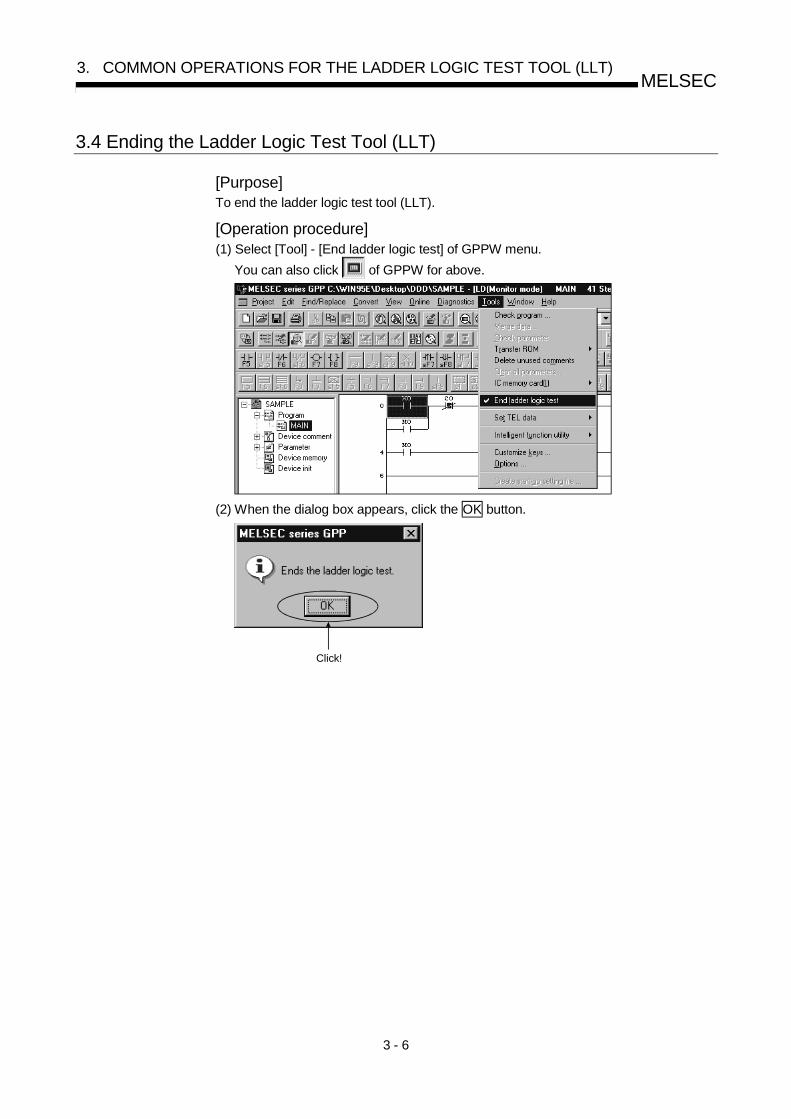
3 - 6
MELSEC3. COMMON OPERATIONS FOR THE LADDER LOGIC TEST TOOL (LLT)
3.4 Ending the Ladder Logic Test Tool (LLT)
[Purpose]To end the ladder logic test tool (LLT).
[Operation procedure](1) Select [Tool] - [End ladder logic test] of GPPW menu.
You can also click of GPPW for above.
(2) When the dialog box appears, click the OK button.
Click!

4 - 1
MELSEC
4. SIMULATION OF EXTERNAL DEVICE OPERATION --- I/O SYSTEMSETTING FUNCTIONS
4
4. SIMULATION OF EXTERNAL DEVICE OPERATION ---I/O SYSTEM SETTING FUNCTIONS
The I/O system setting functions allow simulation of the operation of external devices.In conventional debugging, a debugging sequence program was created to simulatethe operation of the external devices.Using the I/O system setting functions, the operation of the external devices can beautomatically simulated without the requirement to create a special debuggingsequence program.
(1) Differences between Conventional Debugging and Debugging withthe I/O System Setting FunctionsA comparison between conventional debugging with an actual PLC connectedand debugging using the I/O system setting functions is shown below.(a) Conventional Debugging
The program must be modified as follows for debugging: Add a debugging sequence program to simulate operation of the externaldevices. As an input (X) can be turned ON/OFF only with an external deviceconnected to the I/O unit, modify the program by changing X0 M0, X1
M1, etc. to conduct debugging with no external device connected.
(b) Debugging using the I/O System SettingsThe I/O system setting function allows sequence program settings andchanges to be made for debugging from the setting window.It is unnecessary to add a sequence program. It is not necessary to rewritethe devices (X0 M0) as the inputs (X) can be directly turned ON/OFFfrom GPPW.
Y0
X0
Y0T0
K50
T0M1
Problem 2: Sequence program for debugging is necessary
X0 X1
Y0
Y0
Y0
SET X1
<Program used in conventional debugging> <Program used for debugging using the ladder logic test tool (LLT)>
Problem 1: Devices must be rewritten
M0 X1 M1
Solution 1: Rewriting of devices is not necessary
Solution 2: Pseudo-sequence program is created in a separate file
5-sec timer setting
5-sec timer
Start Stop Run Start Stop RunY0

4 - 2
MELSEC
4. SIMULATION OF EXTERNAL DEVICE OPERATION --- I/O SYSTEMSETTING FUNCTIONS
(2) Conditions for simulationWith I/O system setting, optional operation will be performed after the condition is
fulfilled.
By combining conditions, conditions equivalent to the following circuits can be
set.
X0 X1
X0
X2
X0
X0 X1
X2
X0 X1
X2
X0 X1
X3
X0 X1
X2 X3

4 - 3
MELSEC
4. SIMULATION OF EXTERNAL DEVICE OPERATION --- I/O SYSTEMSETTING FUNCTIONS
(3) Timing chart input and device value inputWith I/O system setting, there are two inputs: one is timing chart input to execute
timing chart prepared by user after condition is fulfilled; the other is device value
input to set optional device value after specified time has elapsed.
Differences between the above two inputs are described below.(a) Timing chart input
When condition set by user has been fulfilled, timing chart set by the user
can be operated.
With this input, complicated operations, such as "When Y0 is turned ON, D0
is counted up, Y0 is turned OFF when X0 is turned ON", can be set.
However, the timer cannot be set: If timer is to be used, select device value
input.
<Timing chart format input screen>
(b) Device value inputWhen condition set by user has been fulfilled, specified device value can be
changed after an optional time has elapsed.
With this input, an operation such as "When Y0 is turned ON, 5 seconds
later X0 and X3 are turned ON" can be set.

4 - 4
MELSEC
4. SIMULATION OF EXTERNAL DEVICE OPERATION --- I/O SYSTEMSETTING FUNCTIONS
4.1 I/O System Setting Operation Procedure
Operation procedure for I/O system setting is shown below.
Start
Save file(see Section 4.8.1).
End
YES
NO
YES
NO
Execute I/O system setting(see Section 4.7).
YES
NO Start monitoring(see Section 4.8.3).
Set I/Osystem by inputting
device value?
Input device value to beset (see Section 4.6).
Set I/O systemby timing chart?
Set using timing chart(see Section 4.4).
Start monitoring withI/O system setting?

4 - 5
MELSEC
4. SIMULATION OF EXTERNAL DEVICE OPERATION --- I/O SYSTEMSETTING FUNCTIONS
4.2 Start and End of I/O System Setting
(1) Starting I/O system setting[Purpose]To start I/O system setting.
[Operation procedure]Select [start] - [I/O system settings] from the initial window.
(2) Ending I/O system setting[Purpose]To end I/O system settings.
[Operation procedure]Select [File] - [Exit I/O System Settings] from I/O system settings screen.

4 - 6
MELSEC
4. SIMULATION OF EXTERNAL DEVICE OPERATION --- I/O SYSTEMSETTING FUNCTIONS
4.3 Configuration of I/O System Settings Screen
I/O system settings screen is opened by clicking [Start] - [I/O System Settings] of initial
window. Configuration of I/O system settings screen is shown below.
1)
2)
3)
5)
6)
4)
1) Menu barName of menu that can be used in I/O system settings is displayed.
When menu has been selected, drop-down menu will be displayed and various
functions from this menu can be used.2) Tool bar
From functions assigned by menu bar, those most frequently used are displayed
with buttons.3) File during editing
Displays name of file being edited.4) File being executed.
Displays name of file registered as I/O system execution file.

4 - 7
MELSEC
4. SIMULATION OF EXTERNAL DEVICE OPERATION --- I/O SYSTEMSETTING FUNCTIONS
5) I/O system settings treeSelects setting method of I/O system settings.
• Timing chart input
Double-click column of number to be set: I/O system setting with timing chart
format can now be performed.
Ups to 40 settings (from No. 1 to No. 40) are possible.
• Device value input
Double-click column of number to be set: I/O system setting with device value
set can now be performed.
Ups to 100 settings (from No.1 to No.100) are possible.6) Edit/monitor screen
Editing and monitoring of I/O system settings are performed using this screen.
• In timing chart input mode (see Section 4.4)
• In device value input mode (see Section 4.6)
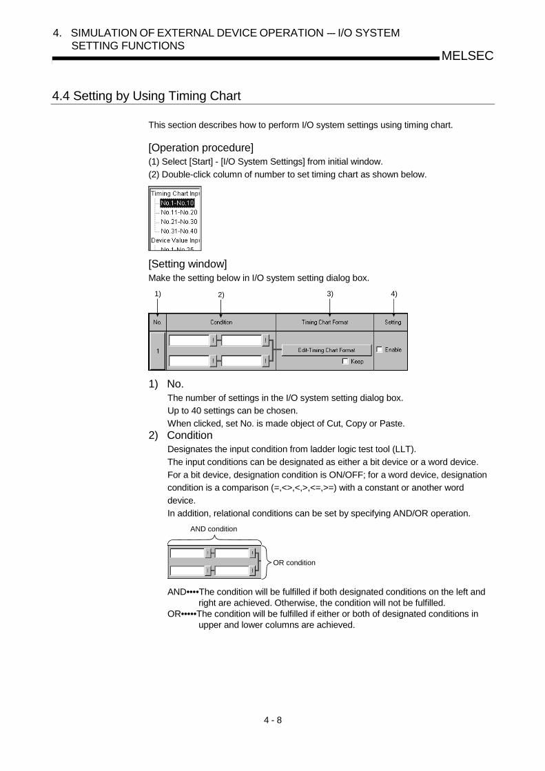
4 - 8
MELSEC
4. SIMULATION OF EXTERNAL DEVICE OPERATION --- I/O SYSTEMSETTING FUNCTIONS
4.4 Setting by Using Timing Chart
This section describes how to perform I/O system settings using timing chart.
[Operation procedure](1) Select [Start] - [I/O System Settings] from initial window.
(2) Double-click column of number to set timing chart as shown below.
[Setting window]Make the setting below in I/O system setting dialog box.
1) 2) 3) 4)
1) No.The number of settings in the I/O system setting dialog box.
Up to 40 settings can be chosen.
When clicked, set No. is made object of Cut, Copy or Paste.2) Condition
Designates the input condition from ladder logic test tool (LLT).
The input conditions can be designated as either a bit device or a word device.
For a bit device, designation condition is ON/OFF; for a word device, designation
condition is a comparison (=,<>,<,>,<=,>=) with a constant or another word
device.
In addition, relational conditions can be set by specifying AND/OR operation.
AND condition
OR condition
AND••••The condition will be fulfilled if both designated conditions on the left andright are achieved. Otherwise, the condition will not be fulfilled.
OR•••••The condition will be fulfilled if either or both of designated conditions inupper and lower columns are achieved.

4 - 9
MELSEC
4. SIMULATION OF EXTERNAL DEVICE OPERATION --- I/O SYSTEMSETTING FUNCTIONS
• Input method (direct input)
Entering condition expression directly can perform setting.
<Example>
For a bit device: X0=OFF, M10=ON
For a word device: D5<20, D15<>5, D20=2, D25>=10, D0=D50
• Input method (entering by using dialog box)
Click button and enter device name, device No., designated condition, etc.
Object of comparison is handled as a 16 bits hexadecimal integer.
When designated as K , setting is done using decimal number, and designated
as H , a hexadecimal number. If neither K nor H is designated, decimal number
setting will be selected.
Refer to Appendix 3(1) for devices that can be entered in the Condition area.
Selects device name. Enters device No.
Selects when"Normally ON" is set.
Selects ON or OFFcondition.
Selects to use as Push button in monitor mode.100 settings (from 0 to 99) can be set with Push button.User can fulfill conditions with optional timing by using the push button.
When a bit device is selected:
Enters device No. Enter object device name and value.
Selects comparison designation.
When a word device is selected:
POINTIndex representation (eg. D0Z0), representation of a word device in bits form (eg.
D0,0), and sets of bits device representation (eg. K4X0) are not allowed in the
Condition area.
3) Timing chart format• Edit-Timing Chart Format button
Click this button: The timing chart format input screen will appear.
Refer to Section 4.5 for operation of screen/
• Continuing
When timing set by timing chart input is to be executed continuously, apply
check mark to check box.4) Setting
Designates enable or disable for each setting.
Apply a check mark to enable the setting.

4 - 10
MELSEC
4. SIMULATION OF EXTERNAL DEVICE OPERATION --- I/O SYSTEMSETTING FUNCTIONS
4.5 Operation of Timing Chart Format Input Screen
This section describes operation of timing chart format input screen.
4.5.1 Operation procedure of timing chart format input screen
The operation procedure of timing chart format input screen is indicated below.
YES
NO
YES
NO
Start
Read timing chartdata file?
Read timing chart data file(see Section 4.5.6).
Register device(see Section 4.5.3).
Set/edit timing(see Section 4.5.4).
Change scan number?
Set scan number(see Section 4.5.5).
End

4 - 11
MELSEC
4. SIMULATION OF EXTERNAL DEVICE OPERATION --- I/O SYSTEMSETTING FUNCTIONS
4.5.2 Configuration of timing chart format input screen
Configuration of timing chart format input screen is described below.
3)
1)
2)
5) 6) 7)
4)
1) Menu barName of menu, which can be used in timing chart format input screen, is
displayed.
When menu has been selected, drop-down menu will be displayed and various
functions from this menu can be used.2) Tool bar
From functions assigned by menu bar, those most frequently used will be
displayed with buttons.3) Device name/device value
Bit device: When timing at cursor position is ON, device name lights (Yellow).
Word device: Device value, with the timing at cursor position, will be displayed in
the text box on the right of device name.
POINT(1) There are three types, Contact, coil and current value, for each expression of
timer (T), Counter (C) and retentive timer (ST) in the timing chart: They are
displayed with following the expressions in the timing chart.Expressions used in timing chart
Timer Counter Retentive timer
Contact TS CS STS
Coil TC CC STC
Present value TN CN STN

4 - 12
MELSEC
4. SIMULATION OF EXTERNAL DEVICE OPERATION --- I/O SYSTEMSETTING FUNCTIONS
POINT(2) Buffer memory and extension file register are displayed as shown below.
<Buffer memory> <Extension file register>
\GU
The first I/O number ofa special function module
Address
\RER
Block No.
Address
When first I/O No. is 4, and address is
K30, "U4\G30" will be displayed.
When block No. is 2, and address is
K30, "ER2\R30" will be displayed.
(3) When a word device is designated as a 32-bit integer, (D) is added to the device
name.
Example: D0(D), W6(D)
4) Scan numberShows scan number of timing.
When scan number is set by selecting [Scan] - [Scan setting], disabled scans will
be displayed with shading.When applying check mark to "Keep" on the right of Edit-Timing Chart Format
button, the enabled scans can be repeated while the condition is being fulfilled.
Example: For continuation with 6 scans designated:
Only 6 scans from 0 to 5 are enabled.
Scans 0 to 5 will be executed repeatedlywhile the condition is being fulfilled.
5) OK buttonDefines settings and exits from this screen.
6) Cancel buttonCancels settings and exits from this screen.
7) StatusDisplays state of timing chart being set.
1 2
4 3
1: Shows that object device wasturned ON from OFF.
2: Shows that object device wasturned OFF from ON.
3: Shows that object device remainsunchanged.
4: Shows that object device haschanged.

4 - 13
MELSEC
4. SIMULATION OF EXTERNAL DEVICE OPERATION --- I/O SYSTEMSETTING FUNCTIONS
4.5.3 Entering/deleting device
(1) Entering device to be simulated[Purpose]To enter device for setting timing.
[Operation procedure](a) Select [Device] - [Enter Device].
(b) Dialog shown below will appear. After setting each item, click Enter button.
A maximum of 16 devices can be entered.
[Bit device selected] [Word device selected]
Item Contents
Device name Selects name of device to be entered.
Device No. Enters device No.
Unit initial address
Displayed when "U" is selected with device name. Enter the higher two digits when
initial I/O No. is expressed in three digits.
Example: In case of X/YIF0, enter "IF".
Initial value
Sets initial value.
For a bit device, select ON/OFF.
For a word device, enter value.
Displayed format
Sets display format of word device to be displayed.
Both decimal and hexadecimal numbers can be set.
Display can be selected from 16 Bit integers, 32 Bit integers and real numbers.
Enter button Enters device.
Close button Closes this screen.

4 - 14
MELSEC
4. SIMULATION OF EXTERNAL DEVICE OPERATION --- I/O SYSTEMSETTING FUNCTIONS
(2) Deleting entered device[Purpose]To delete entered device.
[Operation procedure](a) Select device to be deleted.
Deleting X1F is described here, as example.
(b) Select [Device] - [Delete Device].
Device has been deleted.

4 - 15
MELSEC
4. SIMULATION OF EXTERNAL DEVICE OPERATION --- I/O SYSTEMSETTING FUNCTIONS
4.5.4 Setting/editing timing
This section describes setting and editing method of timing.
(1) Setting the timing of bit deviceTiming of bit device can be set following the procedure shown below.
Move cursor to the timing to be set and operate using any tool button, menu or
short-cut key.
OperationTool
buttonMenu
Short-cut
keyTiming
To turn ON
designated
timing
• [Edit] - [Bit Device] - [Device ON]
• Right-click, then [Device ON]
(Also can be done by double-clicking
cursor position.)
F1
To turn OFF
designated
timing
• [Edit] - [Bit Device] - [Device OFF]
• Right-click, then [Device OFF]
(Also possible to double-click cursor
position.)
F2
To turn OFF until
next ON timing
• [Edit] - [Bit Device] - [Progressive OFF].
• Right-click, then [Progressive OFF].F3
To turn ON until
next OFF timing
• [Edit] - [Bit Device] - [Progressive ON].
• Right-click, then [Progressive ON].F4
To turn OFF
designated
timing and all
later
• [Edit] - [Bit Device] - [All OFF].
• Right-click, then [All OFF].F5
To turn ON
designated
timing and all
later
• [Edit] - [Bit Device] - [All ON].
• Right-click, then [All ON].F6
To insert timing • [Edit] - [Insert]
• Right-click, then [Insert].Insert
To delete timing • [Edit] - [Delete]
• Right-click, then [Delete].Delete
shows cursor position.

4 - 16
MELSEC
4. SIMULATION OF EXTERNAL DEVICE OPERATION --- I/O SYSTEMSETTING FUNCTIONS
(a) Setting ON/OFF period[Purpose]To set ON/OFF continuously, with optional period after designated timing.
[Operation procedure]1) Select initial bit device timing.
2) Operate either of operations shown below.
• Select [Edit] - [Wizard] menu.
• Right-click, select [Wizard] menu.3) Bit device setting wizard screen will appear. Enter scan number and click
OK button.
4) Bit device ON/OFF has been set periodically.

4 - 17
MELSEC
4. SIMULATION OF EXTERNAL DEVICE OPERATION --- I/O SYSTEMSETTING FUNCTIONS
(2) Setting the timing of word device(a) Changing the designated timing value
[Purpose]To change the timing value of designated word device.
[Operation procedure]1) Select timing of word device to be changed.
2) Operate any one of the following operations:
• Select [Edit] - [Word Device] - [Change] menu.
• Right-click, then select [Change] menu.
• Click .
• Enter "F7" key.
• Double-click designated timing.
3) Word device setting wizard screen will appear: Set each item and clickOK button.

4 - 18
MELSEC
4. SIMULATION OF EXTERNAL DEVICE OPERATION --- I/O SYSTEMSETTING FUNCTIONS
Item Contents
Value setting
Set value Enter set value of word device.
Continuation Apply check mark when setting is to be performed continuously.
(Example) Cursor position is scan No. 3, set value is 10, scan number is 4, changed value is 20
increased.
Scan
Value
3 4 5 60
10
30
50
70
Scan Select number of scans to be continued.
Increase & decrease Set to change set value when setting is to be performed continuously.
• Increase: Select when value is to be increased.
• Decrease: Select when value is to be decreased.
Changed value Set increased/decreased value.
Trigonometric functions
SIN curve, COS curve Set when device value is changed as shown below.
(Example) Maximum value is 50, periodical scans are 100.
0
50
-50
10050
Number of scans
0
50
-50
10050
SIN curve COS curve
Number of scans
Maximum value Enter maximum value.
When maximum value is set, minimum value will be set as "-maximum value".
Periodic scan Select number of scans corresponding to 1 period of SIN/COS curve.
4) Word device value has been set.

4 - 19
MELSEC
4. SIMULATION OF EXTERNAL DEVICE OPERATION --- I/O SYSTEMSETTING FUNCTIONS
(b) Fixing unchanged designated timing value[Purpose]To make certain word device value of designated timing is not changed.
[Operation procedure]1) Select word device timing that is not to be changed.
2) Operate any one of following operations:
• Select [Edit] - [Word Device] - [No change] menu.
• Right-click, then select [No change] menu.
• Click .
• Enter "F8" key.
Mark of scan No.2 has been changed.
(C) Inserting timing[Purpose]Insert the timing before designated timing.
Timing is inserted to the left side of cursor position.
[Operation procedure]1) Select the timing at the right side of the position where timing is to be
inserted.

4 - 20
MELSEC
4. SIMULATION OF EXTERNAL DEVICE OPERATION --- I/O SYSTEMSETTING FUNCTIONS
2) Operate any one of the following operations.
• Select [Edit] - [Insert] menu.
• Right-click, then select [Insert] menu.
• Click .
• Enter "Insert" key.
After timing has been inserted, timing will shift to the right.
(d) Deleting the timing[Purpose]To delete designated timing.
[Operation procedure]1) Select timing of the position to be deleted.
2) Operate any one of the following operations:
• Select [Edit] - [Delete] menu.
• Right-click, then select [Delete] menu.
• Click .
• Enter "Delete" key.
After timing is deleted, timing will shift to the left.

4 - 21
MELSEC
4. SIMULATION OF EXTERNAL DEVICE OPERATION --- I/O SYSTEMSETTING FUNCTIONS
4.5.5. Setting scan number of timing chart
[Purpose]To set scan number of timing input from external device.
[Operation procedure](1) Select [Scan] - [Scan Setting].
(2) Scan number setting screen will appear: Enter scan number.
(Example)
When Scan number is set to 5, and timing chart is set to "Keep", scanning from 0
to 4 will be repeated as long as the condition is fulfilled.
Scanning from 0 to 4 will be repeated as long as the condition is fulfilled.
Only 5 scans from 0 to 4 are effective.

4 - 22
MELSEC
4. SIMULATION OF EXTERNAL DEVICE OPERATION --- I/O SYSTEMSETTING FUNCTIONS
4.5.6 Other operations
(1) Reading data saved using timing chart of device memory monitor
[Purpose]To read and use timing chart data file ( .DAT) saved with timing chart.
When the file is read, device and timing will be automatically registered. It is not
necessary to re-enter them.
[Operation procedure]Select [File] - [Open File].
[Setting window]
Designate optional file with "Look in", click file to be opened and click Open
button.
POINTDevices for only 16 points from upper side of timings (maximum 64 points) set by
timing chart screen can be read.
It is necessary to move required timings to upper side before creating timing data
file.
(2) Returning to original state before operation
[Purpose]To return to previous state before last operation performed.
Only the operation immediately before can be regained.
[Operation procedure]Select [Edit] - [Undo].

4 - 23
MELSEC
4. SIMULATION OF EXTERNAL DEVICE OPERATION --- I/O SYSTEMSETTING FUNCTIONS
(3) Displaying registered device listSelect [Device] - [List Device]. Registered device list will be displayed.
• Click Add button. Device registration dialog will be displayed. Refer to Section
4.5.3 (1) for details.• By clicking Delete button, the device is deleted from object of monitoring.
Two or more devices can be deleted by using "Shift key + Select" or "Ctrl key +
Select".• By clicking Jump To button, display of timing chart format input screen jumps to
device being selected.• By clicking UP / DN button, device being selected moves up or down.
• Selecting Two or more devices
(Two or more devices cannot be selected and moved simultaneously.)
(4) Changing display format of word deviceSelect [Word Device]. Then select [Device] - [Property]. Dialog shown below will
appear: Display format can be changed.
• Value
Selects decimal or hexadecimal number display.
• View
Selects 16 Bit, 32 Bit or real number.

4 - 24
MELSEC
4. SIMULATION OF EXTERNAL DEVICE OPERATION --- I/O SYSTEMSETTING FUNCTIONS
(5) Exchanging device display positionDisplay position of device can be exchanged by drag & Drop.
(a) Drag the device name in the timing chart format input screen. Dotted line
frame will appear during dragging.
Drag!
(b) Superimpose dotted line frame on the device name to be exchanged. Device
name can now be exchanged.
Superimpose dotted line frame.
Stop dragging.

4 - 25
MELSEC
4. SIMULATION OF EXTERNAL DEVICE OPERATION --- I/O SYSTEMSETTING FUNCTIONS
4.6 Setting by Entering Device Value
This section describes I/O system setting by entering device value.
[Operation procedure](1) Select [Start] - [I/O System Settings] from initial window.
(2) Double-click column of number to which device value is to be set.
[Setting window]Perform setting in I/O system setting dialog box as shown below.
1) 2) 3) 4) 5)
[Description of items]1) No.
Number of settings in I/O system setting dialog box.
Maximum 100 settings can be chosen.
Once the set No. has been clicked, it can be cut, copied or pasted.2) Condition
Since the conditions are the same as those when timing chart is used, refer to
Section 4.4 (2).3) Timer
Sets the time from the point when designated condition is fulfilled until the input is
issued. Enter the time in 10 ms units. The setting range is 1 to 1000 (× 10 ms).4) Input No.
Designates the bit device which is turned ON/OFF once designated condition has
been fulfilled. Also designates word device whose value is to be changed.
Word device designation
Sets bit device ON/OFF whencondition has been fulfilled.
Bit device designation

4 - 26
MELSEC
4. SIMULATION OF EXTERNAL DEVICE OPERATION --- I/O SYSTEMSETTING FUNCTIONS
• Input method (Direct input)
Independent device designation.... Designates non-consecutive devices,
separated by commas (,).
(Example: D0=10,D2=20,D3=50)
Consecutive device designation .... Designates the first and last of a series of
(bit device only) consecutive devices, separated by a hyphen
(-).
(Example: X0-100)
Mixed device designation............... Designates a mixture of independent and
(bit device only) consecutive devices.
(Example: X0, X2, M10-20)
• Input method (using dialog box)
Click button and enter device name and device No., etc.
Refer to Appendix 3 (2) for devices that can be entered in the input No. area.
When word device is selected:
Select device name.Enter No. of first devicewhich is to be turned ON/OFF. Select device name.
Enter No. of lastdevice which is to beturned ON/OFF.
Entered devicewill be displayed.
Device is registered byclicking here.
When bit device is selected:
Enter value to be set(also possible withword device)
Enter device number.
5) SettingDesignates whether each setting is to be enabled or disabled. Apply check mark
to check box for the setting to be enabled.

4 - 27
MELSEC
4. SIMULATION OF EXTERNAL DEVICE OPERATION --- I/O SYSTEMSETTING FUNCTIONS
4.7 Starting/Stopping the Simulation
Refer to Section 7.3 "Using I/O System Settings for Debugging" for example of
simulation.
(1) Starting the simulation[Purpose]To start simulation with contents in I/O system settings.
[Operation procedure](a) Select [File] - [Open] to open I/O system setting file ( .LIM).
Refer to Section 4.8.1 for details of operation.
(b) Select [File] - [Execute I/O System Settings].
(Yellow) can also be clicked instead of above.
(c) Dialog box for confirmation will appear: Click OK button.
[For A/QnA/QCPU] [For FXCPU]
POINTAfter changing I/O system setting of a file being opened, the file can automatically
be saved by executing the I/O system settings.
If I/O system setting file is not to be saved, save the file under a different file name
and execute I/O system settings.

4 - 28
MELSEC
4. SIMULATION OF EXTERNAL DEVICE OPERATION --- I/O SYSTEMSETTING FUNCTIONS
(d) When A/QnA/QCCPU is used, execution state will automatically change from
STOP to RUN mode, and simulation will start.
When FXCPU is used, simulation is started by switching the setting in the
initial window from STOP to RUN.
• When GPPW is SW1D5 -GPPW-E or later
After the ladder logic test tool (LLT) is started, the set I/O system settings will
remain enabled until they are deleted or the ladder logic test tool (LLT) is
quit.
To use the same I/O system settings when the ladder logic test tool (LLT) is
restarted, read the I/O system setting data from the saved file, and then
execute the I/O system setting again.
• When GPPW is SW0D5 -GPPW-E
The I/O system settings made once are effective until [Cancel I/O Settings]
is executed, regardless of starting/ending the ladder logic test tool (LLT).
POINTFor FXCPU: If settings are made in RUN status, the status must be switched to
STOP once before returning to RUN, to enable the new settings.
(2) Stopping the simulation
[Purpose]To stop the I/O system setting operation currently being executed.
[Operation procedure](a) Select [File] - [Cancel I/O System Settings].
Also (White) can be clicked instead of above.
POINTWhen I/O System Settings are not being executed, the I/O system setting LED on
the initial window will turn off.

4 - 29
MELSEC
4. SIMULATION OF EXTERNAL DEVICE OPERATION --- I/O SYSTEMSETTING FUNCTIONS
4.8 Other Operations
4.8.1 Operating the file
(1) Creating a new file
[Purpose]To create a new file ( .LIM) to be used for I/O system settings.
[Operation procedure]Select [File] - [New].
Also can be clicked instead of above.
(2) Opening saved file
[Purpose]To open an I/O system setting file ( .LIM) which has been saved.
[Operation procedure]Select [File] - [Open].
Also can be clicked instead of above.
[Setting window]
Designate optional holder with "Look in", click the file to be opened, then clickOpen button.

4 - 30
MELSEC
4. SIMULATION OF EXTERNAL DEVICE OPERATION --- I/O SYSTEMSETTING FUNCTIONS
(3) Saving the file
[Purpose]To over-write and save the I/O system setting file ( .LIM) being opened.
[Operation procedure]Select [File] - [Save].
can also be clicked instead of above.
If file being opened has not been saved, "Save As" dialog will be displayed:
Save with optional name entered. Refer to (4) for details.
(4) Saving with new name
[Purpose]To save I/O system setting file ( .LIM) that is being opened with new name
entered.
[Operation procedure]Select [File] - [Save As].
[Setting window]
Designate optional folder with "Save in", and enter file name to be saved in "File
name".
If setting is to be over-written on existing file, select the file to be saved byclicking: Then click Save button.

4 - 31
MELSEC
4. SIMULATION OF EXTERNAL DEVICE OPERATION --- I/O SYSTEMSETTING FUNCTIONS
4.8.2 Cutting, copying and pasting all settings in the set No.
(1) Cutting and copying the selected set No.
[Purpose]To cut and copy selected set No. and save on clipboard.
[Operation procedure](a) Select the set No. to be cut/copied by clicking.
(b) For cutting, select [Edit] - [Cut].
can also be clicked instead of above.
For copying, select [Edit] - [Copy].
can also be clicked instead of above.
(2) Pasting the cut/copied set No.
[Purpose]To paste cut/copied set No. to optional position
[Operation procedure](a) Select the set No. to be pasted by clicking.
(b) Select [Edit] - [Paste].
can also be clicked instead of above.
(c) Cut/copied set No. has been pasted.
POINTA set No. copied or cut in device value input mode cannot be pasted with timing
chart input, and vice-versa.

4 - 32
MELSEC
4. SIMULATION OF EXTERNAL DEVICE OPERATION --- I/O SYSTEMSETTING FUNCTIONS
4.8.3 Executing monitoring
(1) Starting monitoring
[Purpose]To start monitoring a device on the I/O system settings screen.
[Operation procedure](a) Select [Online] - [Monitor mode].
can also be clicked instead of above.
(b) Monitoring will start.
Refer to (3) for details of operation on the screen during monitoring.
(2) Stopping monitoring
[Purpose]To stop monitoring with I/O system setting screen.
[Operation procedure]Select [Online] - [Edit mode].
can also be clicked instead of above.
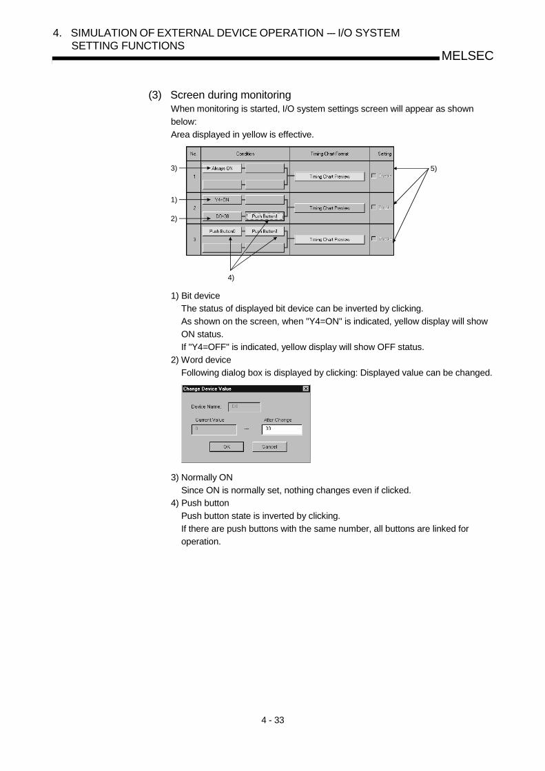
4 - 33
MELSEC
4. SIMULATION OF EXTERNAL DEVICE OPERATION --- I/O SYSTEMSETTING FUNCTIONS
(3) Screen during monitoringWhen monitoring is started, I/O system settings screen will appear as shown
below:
Area displayed in yellow is effective.
3)
1)
2)
4)
5)
1) Bit device
The status of displayed bit device can be inverted by clicking.
As shown on the screen, when "Y4=ON" is indicated, yellow display will show
ON status.
If "Y4=OFF" is indicated, yellow display will show OFF status.
2) Word device
Following dialog box is displayed by clicking: Displayed value can be changed.
3) Normally ON
Since ON is normally set, nothing changes even if clicked.
4) Push button
Push button state is inverted by clicking.
If there are push buttons with the same number, all buttons are linked for
operation.

4 - 34
MELSEC
4. SIMULATION OF EXTERNAL DEVICE OPERATION --- I/O SYSTEMSETTING FUNCTIONS
(5) Timing chart preview buttonTiming chart format input screen is displayed by clicking and the set contents can
be confirmed.
However, the contents of this displayed screen cannot be edited.
4.8.4 Reading I/O system setting file for SW4 or earlier versions
[Purpose]To read I/O system setting file for SW0D5 -LLT-E to SW4D5C-LLT-E.
[Operation procedure]Select [File] - [Import Earlier Version of I/O System File].
[Setting window]
Designate optional folder with "Look in", click the file ( .TXT) to be opened, then clickOpen button.

5 - 1
MELSEC5. MONITORING DEVICE MEMORY MONITOR TEST FUNCTION
5
5. MONITORING DEVICE MEMORY --- MONITOR TESTFUNCTION
The monitor test functions monitor the status of the device memory saved in the ladder
logic test tool (LLT), force bit devices ON/OFF, and test changes to word device
present values.
5.1 GPPW and Ladder Logic Test Tool (LLT) Monitor Test Functions
A combination of the ladder logic test tool (LLT) and GPPW monitor test functions
allows the extensive GPPW monitor test functions to be used offline.
All monitor test functions available with the GPPW and ladder logic test tool (LLT) are
described below.
If the ladder logic test tool (LLT) does not support a function, execute a function from a
GPPW menu.
FunctionFunction Executedfrom a GPPWMenu
Function Executedfrom a LadderLogic Test Tool(LLT) Menu
Ladder monitor
Device batch monitor
Device registration monitor
Buffer memory batch monitor
Device test
Skip execution
Partial execution
Monitor test
functions
Step execution 1
…… Available
…… Not supported
1: For the Q series CPU (Q mode), GPPW cannot be used. Only LLT may be used.
See the SW5D5C-GPPW Operating Manual for details of the functions which can be
executed from the GPPW menu.

5 - 2
MELSEC5. MONITORING DEVICE MEMORY MONITOR TEST FUNCTION
5.2 Operation Procedure of Monitoring Device Memory
Operation procedure of monitoring device memory is shown below:
YES
YES
NO
NO Test the device(see section 5.4.6).
Start
Monitoring usingtiming chart?
Monitor using timing chart(to section 5.5.1 Operationprocedure).
Select the device to bemonitored (see section 5.4.1).
Change device value?
End

5 - 3
MELSEC5. MONITORING DEVICE MEMORY MONITOR TEST FUNCTION
5.3 Starting/Ending Monitoring Device Memory
(1) Starting monitoring device memory
[Purpose]To start monitoring device memory.
[Operation procedure]Select [Start] - [Device Memory Monitor] from initial window.
(2) Ending monitoring device memory
[Purpose]To end monitoring device memory.
[Operation procedure]Select [Start] - [Exit] from device memory monitor screen.

5 - 4
MELSEC5. MONITORING DEVICE MEMORY MONITOR TEST FUNCTION
5.4 Monitoring/Testing the Device Memory
This section describes how to monitor/test the device memory.
This section provides only the functions which are performed from the ladder logic test
tool (LLT) menu. See the SW5D5C-GPPW-E Operating Manual for details of the
functions performed from the GPPW menu.
5.4.1 Selecting the devices for monitoring
This section describes how to select the devices for monitoring.
[Operation Procedure]1) Select [Start] [Device Memory Monitor] from the initial window.
2) Select [Device Memory] then [Bit Device] or [Word Device] in the device
memory monitor window and select the devices to be monitored in the
monitor test.
3) The selected device window is displayed.
The selected device monitor is started automatically.
POINTFor the A series, QnA series, Q series or motion controller CPU functions, always
make I/O assignment setting of GPPW when monitoring the buffer memory of the
special function module.

5 - 5
MELSEC5. MONITORING DEVICE MEMORY MONITOR TEST FUNCTION
4) Click on the button or select [Display] [Jump] (llF9ll) to
change the displayed device range.…………………………... Click this button to display the first page of
currently displayed devices.…………………………... Click this button to display the previous page of
currently displayed devices.…………………………... Click this button to display the next page of
currently displayed devices.…………………………... Click this button to display the last page of
currently displayed devices.[Display] [Jump] (llF9ll)... Select these items to open the following setting
window.
Designate the first device number to bdisplayed.
5) To open multiple windows, select [Window] [New] (llF2ll) and designate
the device names and device numbers.
The designated device windows are displayed overlapping each other.
POINTS(1) Although the device window opens in either procedure of [Device Memory]
[Bit Device] / [Word Device] or [Window] [New] (llF2ll), the device window
called by the procedure beginning with the selection of [Device Memory]
display the devices starting from device number 0.Select [Window] menu (llF2ll) to specify an arbitrary start device number for
display.(2) Pressing the lESCl key closes the device window which is currently active.

5 - 6
MELSEC5. MONITORING DEVICE MEMORY MONITOR TEST FUNCTION
5.4.2 Stopping and restarting the device memory monitor
[Purpose]To stop the device data changes and view the monitor window.
[Operation Procedure]1) Select [Monitor] [Start/Stop] (llF3ll) in the Device memory monitor window
while monitoring the device memory.
2) The device memory monitoring stops.
3) To restart the device memory monitoring, select [Monitor] [Start/Stop](llF3ll) again.
POINTThe present monitor status is displayed in the guidance column below the device
memory monitor window.
During monitoring
During monitor stopped

5 - 7
MELSEC5. MONITORING DEVICE MEMORY MONITOR TEST FUNCTION
5.4.3 Changing the monitor communications interval
[Purpose]To set the interval at which the ladder logic test tool (LLT) device memory status is
monitored.
[Operation Procedure]1) Select [Monitor] [Monitor Interval] in the Device memory monitor window.
2) The monitoring interval dialog box is displayed.
Drag the pointer in the dialog box to set the monitoring interval.Click on the OK button when the setting is complete.
Drag this pointer to set

5 - 8
MELSEC5. MONITORING DEVICE MEMORY MONITOR TEST FUNCTION
5.4.4 Changing the device memory monitor format
[Purpose]To switch the display format of the device monitor column to match the data contents.
[Setting Window]1) 2)
[Description of the Settings]1) View
Selects whether to display the values in the device monitor column in 16-bitunits, 32-bit units, or as a floating decimal-point display when monitoring aword device.The same operation is possible from the keyboard by pressing the lF7l key.16 Bit Integer .........Displays the values in 16-bit units.32 Bit Integer .........Displays the values in 32-bit units.Real .......................Displays the value as a floating decimal point value
(single-precision value).
2) ValueSelects whether to display the values in the device monitor column as adecimal or hexadecimal value when monitoring a word device.The same operation is possible from the keyboard by pressing the lF8l key.Decimal..................Displays a decimal value.Hexadecimal..........Displays a hexadecimal value.
POINTThe device monitor format can also be changed by selecting the desired format
from the drop-down menu of [Display] in the Device memory monitor window.

5 - 9
MELSEC5. MONITORING DEVICE MEMORY MONITOR TEST FUNCTION
5.4.5 Opening the new window
[Purpose]To open a new window, designate the device.
[Operation Procedure]1) Opening a new window
Choose [Window] [New] in the Device Memory window.
Entering the device name and device number and clicking the [OK] button
opens a new window.
POINTYou can open up to 8 windows concurrently.

5 - 10
MELSEC5. MONITORING DEVICE MEMORY MONITOR TEST FUNCTION
5.4.6 Running the device test
[Purpose]To force bit devices ON/OFF or force changes to the present values of word devices
while monitoring the devices.
[Operation Procedure]Select [Device Memory] then [Bit Device] or [Word Device] in the Device memory
monitor window and select the devices to be monitored in the monitor test.
(1) Forcing Bit Devices ON/OFF(a) Double-click on the device number to be turned ON/OFF forcibly in the
bit device monitor window.
Double-click here
(b) Click on the device number to select it and press the F10 key. The
ON/OFF status of the selected bit device is highlighted.
(c) Click on the device number to select it and select [Monitor] – [Test].
(2) Changing Word Device’s Present Values(a) Move the cursor to the present value text box for the word device and
directly input the required value.
Input the required value here
Press the lEnterl key to change the original present value to the
designated value.

5 - 11
MELSEC5. MONITORING DEVICE MEMORY MONITOR TEST FUNCTION
(b) Double-click on the device number.
Calculator screen will appear: Designate present value after changeand click Set button.
(c) Click device number and select [Monitor] - [Test].
Calculator screen will appear: Designate present value after changeand click Set button.
POINTAlways select the hexadecimal display for numeric values when inputting a
hexadecimal using the numeric keypad. Note that character-string cannot be input.

5 - 12
MELSEC5. MONITORING DEVICE MEMORY MONITOR TEST FUNCTION
5.5 Using Timing Chart
By using timing chart, timing of ON/OFF for bit device and change in word device value
can be confirmed easily.
5.5.1 Operation procedure of timing chart
Operation procedure of timing chart is shown below:
YES
NO
End
Start
Start up timing chart(see Section 5.5.2).
Entry of deviceEntry with auto mode.
Enter device in auto mode(see Section 5.5.4 (1)(a)).
Entry device inmanual mode.
Enter device in manualmode (see Section 5.5.4 (1)(b)).
Start monitoring(See Section 5.5.5).
Save entereddevice in file?
Save in file(see Section 5.5.6 (2)).
REMARK
When sampling period is to be set, refer to Section 5.5.7.
Refer to Section 5.5.6 (3) if saved as timing chart data file.

5 - 13
MELSEC5. MONITORING DEVICE MEMORY MONITOR TEST FUNCTION
5.5.2 Starting/exiting timing chart
(1) Staring timing chart
[Purpose]To start timing chart.
[Operation procedure]Select [Timing Chart] - [Run] from device memory monitor screen.
Maximum 4 timing charts can be started.
(2) Exit timing chart
[Purpose]To exit timing chart.
[Operation procedure]Select [File] - [Exit] from timing chart screen.

5 - 14
MELSEC5. MONITORING DEVICE MEMORY MONITOR TEST FUNCTION
5.5.3 Using timing chart
(1) Screen display/operationWhen you run Timing Chart, the following Timing Chart screen appears.
The following gives the explanations of the display data of the Timing Chart
screen.
3) 4)
1)
2)
5)
8) 7)
6)
1) Menu barNames of menu that can be used in timing chart are displayed.
When menu is selected, drop-down menu will be displayed and you can use
various functions from this menu.
2) "Status" buttonBy clicking the "Status" button, you can start/stop monitoring.
For the details, refer to Section 5.5.5.
3) Device EntrySelects auto or manual entry of device to be monitored.
For the details, refer to Section 5.5.4.
4) Range of Chart DisplayWhen the sampling interval is set to per scan, the chart display range is
enlarged by 1, 2, 5, 10, and 20 times.

5 - 15
MELSEC5. MONITORING DEVICE MEMORY MONITOR TEST FUNCTION
5) Device name/Device valueBit device ................. When a device is in ON status, the device name lights
up (Yellow). Clicking on the device name will highlight
either ON and OFF of the device.
Word device ............ Displays the device value in an edit box at the right side
of the device name. Double clicking on the device
value will edit the device value.
POINTS(1) The expressions in the timing chart are timer (T), counter (C), and retentive
timer (ST), and each of them has three types; contact, coil, and present value.
In the timing chart, they are expressed as follows.
TS CS STS
TC CC STC
TN CN STN
Expressions used in the timing chart
Timer Counter Retentive timer
Contact
Coil
Presentvalue
(2) Buffer memory and extension file register are displayed as follows.
<Buffer momory> <Extension file register>
\GU
The first I/O number ofa special function module
Address
\RER
Block No.
Address
When the first I/O number is 4 When the block No. is 2 and the
and the address is K30, they are address is K30, they are displayed
displayed as "U4\G30". as "ER2\R30".
(3) When word device is designated as 32 bit integer, (D) is added to the end of
device name.
Example: D0(D), W6(D)
6) Reference line/scaleThe scale displayed indicates the past scan count.Clicking the scale moves the reference line (vertical line) and shows thedevice values at that scan in 5).
7) Scroll barUp to 1000 sampled past states of devices area saved.By operating the scroll bar, you can confirm the past states of devices.

5 - 16
MELSEC5. MONITORING DEVICE MEMORY MONITOR TEST FUNCTION
8) Status displayShows the states of the monitor devices.
1 2
3 4
1 denotes that the corresponding device turned from OFF to ON.
2 denotes that the corresponding device turned from ON to OFF.
3 denotes that the value of the corresponding device remains unchanged.
4 denotes that the value of the corresponding device has changed.

5 - 17
MELSEC5. MONITORING DEVICE MEMORY MONITOR TEST FUNCTION
5.5.4 Entering/deleting device to be monitored
(1) Entering device to be monitored(a) Automatic setting
[Purpose]Automatically enters device used with sequence program.
[Operation procedure]1) Make sure that device entry is set to "AUTO":
If set to "MANUAL", switch to "AUTO".
2) Select [Monitor] - [Start/Stop] to set to monitor mode.You can also click Monitor Stop button instead of above.
3) Device displayed on GPPW screen will automatically be registered as
device, and monitoring will start. (Maximum 64 devices can be entered.)
If displayed device is changed by scrolling the screen, device entry will
automatically change.
Device monitored with GPPWwill be displayed on timingchart screen.
<GPPW screen>
<Timing chart screen>

5 - 18
MELSEC5. MONITORING DEVICE MEMORY MONITOR TEST FUNCTION
POINTS(1) If devices registered using GPPW do not appear in the timing chart screen,
switch the device entry setting from Auto to Manual, and execute device entry.
(2) For any instruction whose argument occupies double-word positions, two word
devices will be displayed on the timing chart screen.
(For DINC D0, D0 and D1 are entered.)
(3) When batch monitor of GPPW is used to monitor a bit device, this bit device will
not be entered.
(4) When the A/FX/Q (A mode)/motion controller CPU is selected, the bit digit-
specified/index-qualified device will not be entered.
(5) When QnA/QCPU (Q mode)is selected, directly designated buffer memory will
not be entered.
(6) When FX series CPU is selected, the following instructions displayed on GPPW
circuit monitor screen will not be entered.
RST T, RST C
PLS Y, PLS M
PLF Y, PLF M
(b) Manual entry[Purpose]Manually enters device to be monitored in timing chart.
[Operation procedure]1) Select [Device] - [Enter Device].
2) The dialog shown below will appear: After setting each item, click Enter
button.
Maximum 64 devices can be entered.<"Selection" selected> <"Key input" selected>
Selects device nameto be entered. Designates
device No.
Selects display formatof device to be displayed.
Directly enters
device name.

5 - 19
MELSEC5. MONITORING DEVICE MEMORY MONITOR TEST FUNCTION
(2) Deleting registered device
[Purpose]To delete registered devices.
[Operation procedure](a) Select the device to be deleted:
For example, X0 is deleted here.
(b) Select [Device] - [Delete Device].
Device has been deleted.

5 - 20
MELSEC5. MONITORING DEVICE MEMORY MONITOR TEST FUNCTION
5.5.5 Starting/stopping monitoring
(1) Starting monitoring
[Purpose]To start monitoring the timing chart.
[Operation procedure]After registering device, select [Monitor] - [Start/Stop] while monitor is stopped.You can also click Monitor Stop button instead of above.
However, if device is registered in AUTO mode, monitoring will start when device
is registered.
(2) Stopping monitoring
[Purpose]To stop monitoring timing chart.
[Operation procedure]Select [Monitor] - [Start/Stop] during monitoring.You can also click Monitoring button instead of above.

5 - 21
MELSEC5. MONITORING DEVICE MEMORY MONITOR TEST FUNCTION
5.5.6 Operating file
(1) Opening saved file
[Purpose]To open device registration file ( .MON) that have been saved.
[Operation procedure]Select [File] - [Open file].
[Setting window]
Designate optional folder with "Look in", click file to be opened, then click Open
button.
(2) Saving in file
[Purpose]To save entered device as a device registration file ( .MON).
[Operation procedure]Select [File] - [Save File As].

5 - 22
MELSEC5. MONITORING DEVICE MEMORY MONITOR TEST FUNCTION
[Setting window]
Designate optional folder with "Save in", and enter new file name in "File name".
If data is to be overwritten on existing file, select the file by clicking.After setting, click Save button.
(3) Saving as timing chart data file
[Purpose]To save as a timing chart data file.
Timing chart data file can be read using timing chart format input of I/O system
settings.
[Operation procedure]Select [File] - [Save Timing data].
[Setting window]
Designate optional folder with "Save in", and enter new file name in "File name".
If data is to be overwritten on existing file, select the file by clicking.After setting, click Save button.

5 - 23
MELSEC5. MONITORING DEVICE MEMORY MONITOR TEST FUNCTION
5.5.7 Setting sampling period
[Purpose]To set collection interval of device value in the range between 1 and 20 scans.
[Operation procedure](1) Select [Monitor] - [Sampling Period].
(2) Sampling period setting screen will appear: Input data collection interval.
<Example>
When Data Accumulation Interval is set to 5 scans, the device value will be
collected every 5 scans and displayed in the timing chart display screen.
(The default value is 1 scan.)
REMARK
Every time you change the sampling period, the data displayed in the timing chart
will be cleared.

5 - 24
MELSEC5. MONITORING DEVICE MEMORY MONITOR TEST FUNCTION
5.5.8 Other operations
(1) Displaying the list of registered devicesSelect [Device] - [List Device]: The list of registered devices will be displayed.
• Click Enter button: Device entry dialog will appear.
Refer to Section 5.5.4 for details.• Click Delete button: The device will be deleted from target of monitoring.
By using "Shift key + Select" or "Ctrl key + Select", two or more devices can be
deleted simultaneously.• Click Jump To button: Timing chart being displayed will jump to selected
device.• Click / button: Device being selected will move up/down.
• Selecting two or more devices
(You cannot select two or more devices for moving.)
(2) Changing word device display formatSelect "Word Device" and select [Device] - [Property]. The dialog shown below
will appear: Display format can now be changed.
• Value
Changes between decimal and hexadecimal.
• View
Changes between 32 bit integer and Real number.
(Effective only when selected device is a double word)

5 - 25
MELSEC5. MONITORING DEVICE MEMORY MONITOR TEST FUNCTION
(3) Exchanging display position of deviceDragging and dropping device name can exchange the device displayed position.
(a) Drag device name of the timing chart screen.
During dragging, a white square frame will appear.
Drag!
(b) By superimposing white square frame on the device name to be exchanged,
device name can be exchanged.
Superimpose white square frame.
Stop dragging.

5 - 26
MELSEC5. MONITORING DEVICE MEMORY MONITOR TEST FUNCTION
(4) Viewing the status changes of the devices monitoredThe ladder logic test toll (LLT) can save up to 1000 samples of past states of
devices.
The following example shows how to confirm the device status of 260 scans
before.
(a) Set the monitoring state of timing chart to stop.
(b) Operate the scroll bar until -260 appears on the timing chart screen.
Click "-260"on the screen.
Click!
Operate the scroll bar.
(c) By clicking "-260", the device status of 260 scans before will appear in 1.
In 1, the bit device ON/OFF status and word device value are displayed.
1
This indicates that when both Y70 andC0 turned OFF, T2 started count.

5 - 27
MELSEC5. MONITORING DEVICE MEMORY MONITOR TEST FUNCTION
5.5.9 Usable devices in the timing chart
The device names that can be used (displayed) in the timing chart are shown
below.
A series CPU Functions, Motion Controller CPU Function
Q series CPU (A Mode) Functions
Symbols Displayed
on WindowDevice Name
X Input
Y Output
M Internal relay
F Annunciator
B Link relay
TS Timer (contact)
TC Timer (coil)
CS Counter (contact)
CC Counter (coil)
Bit device
Sp.M Special relay
TN Timer (Current value)
CN Counter (Current value)
D Data register
W Link register
Buffer Memory Buffer memory
R File register
ER Extension file register
Z
VIndex register
A Accumulator
Word
device
Sp.D Special register
FX series CPU Functions
Symbols Displayed
on WindowDevice Name
X Input
Y Output
M Internal relay
S State
TS Timer (contact)
TC Timer (coil)
CS Counter (contact)
CC Counter (coil)
Bit device
Sp.M Special relay
TN Timer (Current value)
CN Counter (Current value)
D Data register
Buffer Memory Buffer memory
Z
VIndex register
Word
device
Sp.D Special register
QnA series CPU Functions
Q series CPU (Q Mode) Functions
Symbols Displayed
on WindowDevice Name
X Input
Y Output
M Internal relay
L Latch relay
F Annunciator
V Edge relay
SB Special link relay
B Link relay
SM Special relay
TS Timer (contact)
TC Timer (coil)
STS Retentive timer (contact)
STC Retentive timer (coil)
CS Counter (contact)
CC Counter (coil)
FX Function input
Bit device
FY Function output
TN Timer (Current value)
STNRetentive timer
(Current value)
CN Counter (Current value)
D Data register
W Link register
SW Special link register
SD Special register
R File register
ZR Serial file register
Z Index register
Word
device
U Buffer memory

5 - 28
MELSEC5. MONITORING DEVICE MEMORY --- MONITOR TEST FUNCTION
MEMO

6 - 1
MELSEC
6. SAVING AND READING THE DEVICE AND BUFFER MEMORIES ---TOOL FUNCTIONS
6
6. SAVING AND READING THE DEVICE AND BUFFERMEMORIES --- TOOL FUNCTIONS
The tool functions are functions to save the contents of the device memory or special
function unit buffer memory at any time and to read the saved data to the ladder logic
test tool (LLT).
The tool functions allow the contents of the ladder logic test tool (LLT) device memory
or special function unit buffer memory to be saved during debugging. The saved data
can then be read to the ladder logic test tool (LLT) when debugging is repeated, to
allow debugging to be continued from the status when the data was saved.
6.1 Saving the Device and Buffer Memories
[Purpose]To temporarily save the contents of the device memory and buffer memory to allow
debugging to continue after the personal computer is re-booted.
[Operation Procedure]1) Set the execution status in the initial window to STOP when the device
memory or buffer memory contents are to be saved.
2) Select [Tools] [Backup device memory] or [Backup buffer memory].

6 - 2
MELSEC
6. SAVING AND READING THE DEVICE AND BUFFER MEMORIES ---TOOL FUNCTIONS
[Setting Window]
Click on the Yes button, to save the entire device memory or the buffer memory for the
slots allocated to special function units in the I/O assignment settings.
The buffer memory data is saved to the following directories:
A series CPU Functions(Directory where the ladder logic test tool (LLT) are installed) \Acpu\Devmem
QnA series CPU Functions(Directory where the ladder logic test tool (LLT) are installed) \QnAcpu\Devmem
FX series CPU Functions(Directory where the ladder logic test tool (LLT) are installed) \FXcpu\Devmem
Motion controller CPU Functions(Directories where the ladder logic test tool (LLT) are installed)\Acpu\Devmem
Q series CPU Functions(Directory where the ladder logic test tool (LLT) are installed) \Qcpu\Devmem
[Example]If C:\Melsec\LLT is designated as the directory where the ladder logic test tool (LLT)
are installed, then the buffer memory data is saved to the following directories:
A series CPU Functions................... C:\Melsec\LLT\Acpu\Devmem
QnA series CPU Functions.............. C:\Melsec\LLT\QnAcpu\Devmem
FX series CPU Functions..................C:\Melsec\LLT\FXcpu\Devmem
Motion controller CPU Functions..... C:\Melsec\LLT\Acpu\Devmem
Q series CPU Functions .................. C:\Melsec\LLT\Qcpu\Devmem
POINTS(1) If the execution status is RUN, device memory/buffer memory cannot be
saved.
To save the device memory/buffer memory, change the status to STOP.
(2) The ladder logic test tool (LLT) can save only one file.
If data already exists in the ladder logic test tool (LLT), the new file overwrites
the existing data (file).

6 - 3
MELSEC
6. SAVING AND READING THE DEVICE AND BUFFER MEMORIES ---TOOL FUNCTIONS
6.2 Reading Saved Device Memory or Buffer Memory Data
[Purpose]To read the stored data of device memory and buffer memory.
[Operation Procedure]Set the execution status in the initial window to STOP. Select [Tools] [Restore
device memory] or [Restore buffer memory].
[Setting Window]
Reading device memory
1)
3) 4) 5)
3) 4) 5)
<A series CPU, Motion controller CPU and Q series CPU (A Mode)> <QnA series CPU and Q serise CPU (Q Mode )>
<FX series CPU>
3) 4) 5)
1)

6 - 4
MELSEC
6. SAVING AND READING THE DEVICE AND BUFFER MEMORIES ---TOOL FUNCTIONS
Reading buffer memory
2)
3) 4) 5)
<A series CPU, QnA series CPU, Motion controller CPU and Q serise CPU >
<FX series CPU>
3) 4) 5)
2)

6 - 5
MELSEC
6. SAVING AND READING THE DEVICE AND BUFFER MEMORIES ---TOOL FUNCTIONS
[Description]1) Read Device Check Boxes
Click in the check boxes to select the devices read to ladder logic test tool
(LLT).
Click on a check box again to cancel a selection.
All devices are selected by default.
2) Read Special Function Module Check BoxesFor A series, QnA series, Motion controller or Q series CPU functions, the
special function module first I/O number is displayed at the top of the
window.
The special function module block number or module block number is
displayed at the top of the FX series window.
Click the check box to select the special function module to be read to the
ladder logic test tool (LLT).
Click on a check box again to cancel a selection.
All special function modules are selected by default.
Only the special function module buffer memory can be read.
3) [CLEAR] buttonClick to clear all device or special function module selections.
4) [SELECT ALL] buttonClick to select all devices or special function modules.
5) [OK] buttonClick this button after completing all settings.
POINTS(1) Device memory/buffer memory read is not allowed while the execution status
is RUN.
Change the execution status to STOP before reading device memory/buffer
memory.
(2) With the A series, QnA series, Q series, Motion controller CPU functions,
selection of a slot that is not assigned to a special function module using the
GPPW I/O assignment setting is not possible.
Before reading buffer memory, set the GPPW I/O assignment.

6 - 6
MELSEC
6. SAVING AND READING THE DEVICE AND BUFFER MEMORIES ---TOOL FUNCTIONS
MEMO

7 - 1
MELSEC7. EXAMPLES OF LADDER LOGIC TEST TOOL (LLT) APPLICATIONS
7
7. EXAMPLES OF LADDER LOGIC TEST TOOL (LLT)APPLICATIONS
This chapter provides examples of debugging an actual program using the ladder logic
test tool (LLT).
In this manual, explanations are given using the system configuration shown below
and program shown on page 7-2.
[Simulation Example]The following shows the system where sheet is fed using roller and cut by cutter.
Rotation amount of roller is taken into high-speed counter unit (Channel 1 is used),
roller stops when the value reaches "1000" and sheet is cut by Y20 (cut request).
Roller turns again by X10 (cut completion) from cutter to feed sheet.
[System Configuration]
QCPU
QD62
QX10
QY10
D0
X/Y
0 to
X/Y
F
X10
to X
1F
X20
to X
2F
Pow
er s
uppl
ym
odul
e
Roller
Cutter
Sheet
Motor
Encoder
Y20 (cut request)
X10 (cutcompletion)
POINTProgram, device registration file ( .MON), and I/O system setting file ( .LIM) are
stored in "Manual" folder of CD-ROM for the product.

7 - 2
MELSEC7. EXAMPLES OF LADDER LOGIC TEST TOOL (LLT) APPLICATIONS
[Sequence program]

7 - 3
MELSEC7. EXAMPLES OF LADDER LOGIC TEST TOOL (LLT) APPLICATIONS
[Devices used]
Device No. Signal name Contents
X0 Unit ready Turns ON when high-speed counter unit is ready for start.
X2
Counter value
matching
(point No.1)
Turns ON when present value matches the preset value of matching
output point. Turns ON when value reaches "1000" in this example.
Y0Matching signal No.
1 reset commandTurns ON to turn X2 OFF.
Y1 Preset commandTurns ON when executing preset functions.
In this example, present value is set to "0" when preset is executed.
Y2Matching signal
enable command
Turns ON when matching signal is output to external terminal.
In this example, it can be ignored.
High-speed counter
unit signals
Y4Count enable
command
Starts high-speed counter unit.
Count can be executed only when this signal is turned ON.
X10 cutting completeTurns ON when cutting of sheet is completed.
Turns OFF when Y20 is turned OFF.Cutter operation
control signalsY20 Cut request Turns ON when sheet cutting is to be executed.
X15 Count operation start Turns ON when executing count with high-speed counter unit.
X16Present value
readingTurns ON when reading present value of high-speed counter unit.Signals for ON/OFF
by user
X17Matching output data
setting
Turns ON when matching signal is externally output.
Normally turns ON when matching signal is used.
M10Initial setting
completeSignal to inhibit initial setting at scan 2 or after.
Other devices
D0 to D1Present value
storageDevice to store present value.

7 - 4
MELSEC7. EXAMPLES OF LADDER LOGIC TEST TOOL (LLT) APPLICATIONS
7.1 Debugging Using GPPW Step Execution Function
Using GPPW independently, it is not possible to turn arbitrary devices ON/OFF or to
change device values during step execution. However, using the ladder logic test tool
(LLT) allows the device values to be easily changed during step execution.
In this section, example of debugging with step execution jointly used with following
program is described.
Running the program on page 7-2 and turning on X0 causes "SP. UNIT ERROR" to
occur.
Carry out step execution to find out the step at which the error has taken place.
(1) Pre-debugging operation1) Start GPPW and create the program on page 7-2.
2) Choose [Tools] [Start ladder logic test] on GPPW to start the ladder logic
test tool (LLT). (At a start, the parameters and program are automatically
written and SWITCH changes to RUN.)
(2) Step execution1) Set SWITCH of the ladder logic test tool (LLT) to STEP RUN.
2) Turn on X0.
3) Move the cursor to the position where step execution will be started (step 0).

7 - 5
MELSEC7. EXAMPLES OF LADDER LOGIC TEST TOOL (LLT) APPLICATIONS
4) Select [Online] [Debug] [Debug] on GPPW.
In addition, select [Online] [Debug] [Step execution] on GPPW.
The Step Execution dialog box then appears.
5) Every time you click the Step excutel button in the Step Execution dialog box,
one instruction is executed.
6) As you click the Step excutel button to run the program on an instruction-by-
instruction basis, you will know that "SP. UNIT ERROR" occurs when [DTOP
H0 H0 K0 K1] is executed.
POINT"SP. UNIT ERROR" occurred because you attempted to write a value to the buffer
memory using the TO instruction, without making I/O assignment.
Section 7.2 gives a debugging example in which I/O assignment is made and the
buffer memory is used.
7) Double-click "Parameter" - "Set PLC parameter" from project data list on
GPPW and click "I/O assignment" tab so that I/O assignment is as shown
below.
Slot Type Model Points
0 0 (0-0) Special QD62 16 points
1 0 (0-1) Input QX10 16 points
2 0 (0-2) Output QY10 16 points
8) By updating parameter with PLC writing and setting to RUN after resetting,
error will not occur even if X0 is turned ON.

7 - 6
MELSEC7. EXAMPLES OF LADDER LOGIC TEST TOOL (LLT) APPLICATIONS
7.2 Using Timing Chart Display for Debugging
This section explains how to check device value changing timings with the timing chart
which displays the device chart using the ladder logic test tool (LLT).
(1) Pre-debugging operation1) Start GPPW and create the program on page 7-2.
2) Double-click "Parameter" - "PLC parameter" of project data list on GPPW, click
the "I/O assignment" tab, and make I/O assignment as indicated below.
Slot Type Model Points
0 0 (0-0) Special QD62 16 points
1 0 (0-1) Input QX10 16 points
2 0 (0-2) Output QY10 16 points
3) Choose [Tools] [Start ladder logic test] on GPPW to start the ladder logic
test tool (LLT). (At a start, the parameters and program are automatically
written and SWITCH changes to RUN.)
4) Select [Start] - [Device Memory Monitor] from initial window of Ladder Logic
Test tool (LLT), and start device memory monitor.
(2) Displaying the timing chart1) Running the timing chart
Choose [Timing Chart] [Run] of Device Memory Monitor to run the timing
chart.
2) Register device and start monitoring.
Register the following devices and click "Monitor Stop" button to start
monitoring.
• X0, X2, X10, X15, X16, X17, Y0, Y1, Y2, Y4, Y20, M10, D0 (Double word)
3) Turning X0, X15 and X17 ON (initial setting)
X0, X15 and X17 are turned ON in sequence.
When X0 is turned ON, M10 is turned ON, in like manner X15: Y4, and X17:
Y2.
POINTThe timing chart retains data of up to 1000 scans.

7 - 7
MELSEC7. EXAMPLES OF LADDER LOGIC TEST TOOL (LLT) APPLICATIONS
Double-click hereto change betweenON and OFF.
Turning on X0,turns on M10.
Turning on X15,turns on Y4.
Turning on X17,turns on Y12.
<Actual machine state>
Motor
Roller
Cutter
Sheet
4) Turning X2 ON (Sheet feeding complete start cutting)
Assuming that present value of high-speed counter unit matches the matching
output point No. 1 (reaches 1000), turn X2 ON.
When X2 is turned ON, Y4 is turned OFF to stop roller operation, and cutter
executes cutting by turning Y20 ON.
Turnning on X2,turns off Y4 and turns on Y20.

7 - 8
MELSEC7. EXAMPLES OF LADDER LOGIC TEST TOOL (LLT) APPLICATIONS
<Actual machine state>
Sheet
Motor
RollerCutter
5) Turn X10 ON (cutting complete)
Assuming that cutting is complete, signal X10 sent from cutter turns ON.
When X10 is turned on, Y20 is turned OFF and YO is turned ON.
When Y 20 is turned ON, cutter turns OFF X10. Turn X10 OFF manually.
Turn X10 OFF manually.
Turning X10 ON turns
Y0 ON and Y20 OFF.
<Actual machine state>
Cut SheetRoller
Motor
Cutter

7 - 9
MELSEC7. EXAMPLES OF LADDER LOGIC TEST TOOL (LLT) APPLICATIONS
6) Turn X2 OFF (Re-starting operation)
When Y0 is turned ON, high-speed counter unit turns X2 OFF. Turn X2 OFF
manually.
When X2 is turned OFF, Y0 is turned OFF, Y1 ON and then OFF and Y4 ON.
By turning Y4 ON, roller re-starts operation.
General operation of program is now complete.
When X2 is turned OFF,Y0 is turned OFF, Y1 isturned ON for one scanand Y4 is turned ON.
<Actual machine state>
Sheet
Roller
Cutter
Motor

7 - 10
MELSEC7. EXAMPLES OF LADDER LOGIC TEST TOOL (LLT) APPLICATIONS
7.3 Using I/O System Settings for Debugging
This section describes the operation to perform simulation of external equipment using
the I/O system setting.
(1) Pre-debugging operation1) Start GPPW and create the program on page 7-2.
2) Double-click [Parameter] - [PLC parameter] of project data list on GPPW and
click "I/O assignment" tab so that I/O assignment is as shown below.
Slot Type Model Points
0 0 (0-0) Special QD62 16 points
1 0 (0-1) Input QX10 16 points
2 0 (0-2) Output QY10 16 points
3) Select [Tool] - [Start ladder logic test] on GPPW to start ladder logic test tool
(LLT). (Once started, parameter and program will be automatically written and
execution state is set to RUN.)
4) Select [Start] - [I/O System Settings] on initial window of Ladder logic test tool
(LLT) to start I/O system setting.
(2) Operation of I/O system settings1) Make the following settings.
• Timing chart input
The following setting is performed: D0 is counted up by turning Y4 ON, and
X2 turns ON when count reaches 1000 (matching output).
<Timing chart format input screen>
Count up D0 (32 bit integer) assuming present value.
Turn ON X2 at the moment D0 reaches 1000.
D0: Counted up in 20 count units from 0 to 49th scan.
20 (0 scan), 40, 60, 80 to 1000 (49th scan)
X2: Turned OFF 0 to 48th scan, turned ON only for 49th scan.

7 - 11
MELSEC7. EXAMPLES OF LADDER LOGIC TEST TOOL (LLT) APPLICATIONS
• Device value input
Set No. Contents
1 X0 (unit ready) is normally turned ON.
2
By clicking push button 0, X15 (count operation start) and X17 (matching data setting) which must
be turned ON by user, can be turned ON.
Operation will start by clicking push button 0.
3When Y20 (cut request) is turned ON, X10 (cut complete) turns ON 3 seconds later.
This assumes the operation through cutting has been completed, after requesting cut.
4
When Y0 (matching signal No. 1 reset command) is turned ON, X2 (counter value matching (point
No. 1)) and X10 (cutting complete) are turned OFF.
Operation in which turning Y0 ON turns X2 OFF assumes the operation of high-speed counter unit.
Turing X10 OFF assumes the operation to return cutter signal to initial value.
5When Y1 (preset command) is turned ON, D0 and D1 are set to "0".
This assumes the preset operation of high-speed counter unit.

7 - 12
MELSEC7. EXAMPLES OF LADDER LOGIC TEST TOOL (LLT) APPLICATIONS
2) Save I/O system settings.
3) Select [File] - [Execute I/O System Settings] to execute I/O system setting.
Execution state of ladder logic test tool (LLT) is set to RUN.
4) Select [Online] - [Monitor Mode] to set I/O system setting to monitor mode.
When I/O system setting has been performed, the following pseudo program is
created.
When running program, the pseudo program will be executed after the created
program is executed.

7 - 13
MELSEC7. EXAMPLES OF LADDER LOGIC TEST TOOL (LLT) APPLICATIONS
(3) Displaying timing chartTo confirm the device value, monitor using timing chart.
1) Starting the timing chartSelect [Timing Chart] - [Run] from device memory monitor to start timing
chart.
2) Registering device and starting monitoringRegister the devices shown below and click "Monitor Stop" button to start
monitoring.
• X0, X2, X10, X15, X16, X17, Y0, Y1, Y2, Y4, Y20, M10, D0 (Double word)
(4) Confirming the program operation
1) Click Push button 1. (Initial setting)When Push button 0 of I/O system settings is clicked, operation will start.
By clicking Push button 0, X15 and X17 are turned ON.
Turning X15 ON turns Y4 ON, and turning X17 ON turns Y2 ON. In addition,
DO will be counted up in 20-count units by turning ON Y4.
By clicking Pushbutton 0, X15 andX17 are turned ON.
Y2 is turned ON byturning X17 ON.
Y4 is turned ON byturning X15 ON.
By turning Y4 ON,D0 is counted up.
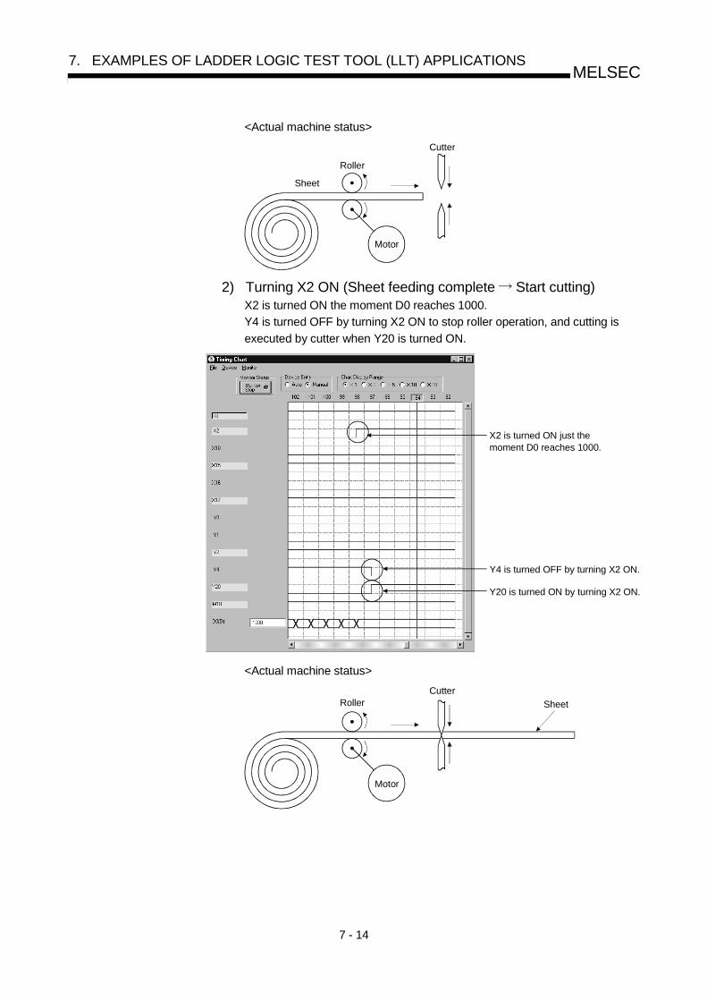
7 - 14
MELSEC7. EXAMPLES OF LADDER LOGIC TEST TOOL (LLT) APPLICATIONS
<Actual machine status>
Motor
Roller
Sheet
Cutter
2) Turning X2 ON (Sheet feeding complete Start cutting)X2 is turned ON the moment D0 reaches 1000.
Y4 is turned OFF by turning X2 ON to stop roller operation, and cutting is
executed by cutter when Y20 is turned ON.
Y20 is turned ON by turning X2 ON.
X2 is turned ON just themoment D0 reaches 1000.
Y4 is turned OFF by turning X2 ON.
<Actual machine status>
Motor
Roller Sheet
Cutter

7 - 15
MELSEC7. EXAMPLES OF LADDER LOGIC TEST TOOL (LLT) APPLICATIONS
3) Turning X10 ON 3 seconds after Y20 is turned ON (Cuttingcompleted)Assuming that 3 seconds is needed until cutting operation is complete, X10
should be turned ON 3 seconds after Y20 is turned ON.
When X10 is turned ON, Y20 is turned OFF and Y0 is turned ON.
Turning on X10,turns on Y0 and turns off Y20.
<Actual machine status>
Motor
Roller Cut sheet
Cutter

7 - 16
MELSEC7. EXAMPLES OF LADDER LOGIC TEST TOOL (LLT) APPLICATIONS
MEMO

8 - 1
MELSEC8. TROUBLESHOOTING
8
8. TROUBLESHOOTING
8.1 Error Messages Displayed on the LED Indicators
This section describes error messages and error codes occurring in the ladder logic
test tool (LLT), gives a description and cause of the error, and suggests remedies.
(1) Ladder Logic Test Tool (LLT) for A series CPU Functions
Error Message Table
Error MessageError Code
(D9008) 1
Details Error
Code
(D9091) ) 1
Error Description and Cause Remedy
101
The program contains an instruction code
which could not be decoded by the ladder
logic test tool (LLT).
102Index qualification used for a 32-bit
constant.
103The device specified in the dedicated
instruction is incorrect.
104The program structure of the dedicated
instruction is incorrect.
105The command name of the dedicated
instruction is incorrect.
"INSTRCT CODE
ERR."
Checked at RUN STOP or at the execution of an instruction
10
107
(1) The index qualification used for
the device number and SV in timer or
counter OUT instructions.
(2) The index qualification used for the
label number of the pointer (P) added at
the start of an instruction jump
destination or for the label number of
the interrupt pointer (I) added at the
start of an interrupt program for the
following instructions.
lCJl lSCJl lCALLl lJMPl
lLEDA/B FCALLl lLEDA/B BREAKl
Read the error step using GPPW
and modify the program step.
121There is no END (FEND) instruction in the
main program.
Write END in the end of main
program.
"MISSING END
INS."
Checked at RUN STOP
12
122
A sub program has been allocated in the
parameters and there is no END (FEND)
instruction.
Write END in the end of the sub-
program.
131
The device number of the pointer (P) or the
interrupt pointer (I) used as a label added to
the destination head is duplicating.
Remove the duplicated number of
pointer (P) with the destination
head and correct so that the
number is not duplicated.
"CAN'T
EXECUTE(P)"
Checked at theexecution of the instruction
13
132
The label of the pointer (P) specified by lCJl
lSCJl lCALLl lCALLPl lJMPl
lLEDA/B FCALLl and lLEDA/B BREAKl
instructions is not specified prior to the END
instruction.
Read the error step using GPPW,
check the step and insert the
destination pointer (P).

8 - 2
MELSEC8. TROUBLESHOOTING
Error Message Table (cont.)
Error MessageError Code
(D9008) 1
Details Error
Code
(D9091) ) 1
Error Description and Cause Remedy
133
(1) There is no lCALLl instruction for the
lRETl instruction in the program.
(2) There is no lFORl instruction for the
lNEXTl, LEDA/B BREAKl instructions
in the program.
(3) The nesting level of lCALLl, lCALLPl, or
lFORl exceeds the nesting limit six (6)
and is executing the sixth level.
(4) There is no lRETl or lNEXTl
instructions for the lCALLl or lFORl
instruction.
(1) Read the error step using
GPPW. Check and modify the
program step.
(2) Nesting level for the lCALLl,
lCALLPl and lFORl instructions
must be five (5) or less.
134
There is no parameter settings for the sub
program. Can not execute the lCHGl
instruction.
Read the error step using GPPW.
Delete the line containing the
lCHGl instruction.
136
There is no parameter settings for sub
program 1. Can not execute the lZCHG1l
instruction.
Read the error step using GPPW.
Delete the line containing the
lZCHG1l instruction.
137
There is no parameter settings for sub
program 2. Can not execute the lZCHG2l
instruction.
Read the error step using GPPW.
Delete the line containing the
lZCHG2l instruction.
"CAN'T
EXECUTE(P)"
Checked at theexecution of the instruction
13
138
There is no parameter settings for sub
program 3. Can not execute the lZCHG3l
instruction.
Read the error step using GPPW.
Delete the line containing the
lZCHG3l instruction.
"WDT ERROR"Checked at the execution of the sequence program.
22 220A program instruction is executed infinitely
in a single scan.
Read the error step and confirm
there is no occurrence of an infinite
loop.
"END NOT
EXECUTE"
Checked at the execution of the instruction.
24 241
The entire program has been executed
without executing the END instruction.
(1) There is no END instruction.
(2) The END instruction is replaced with
some other instruction.
Please write the program to PLC
again.
"SP.UNIT
ERROR"
Checked at theexecution of the FROM/TO instruction or special function module dedicated instruction.
46 461There is no special function module in the
area specified by the FROM/TO instruction.
(1) Read the error step using
GPPW. Check and modify the
FROM/TO instruction in the
program step.
(2) Correct the I/O unit allocation
parameter settings.

8 - 3
MELSEC8. TROUBLESHOOTING
Error Message Table (cont.)
Error MessageError Code
(D9008) 1
Details Error
Code
(D9091) 1
Error Description and Cause Remedy
501
(1) Operations using the file register (R), are
executed with the device number or
block number exceeding the range
specified for the file register (R).
(2) The file register is used in the program
without setting necessary parameters
for the file register (R).
(1) Read the error step using
GPPW. Check and modify the
program step.
(2) Set the parameters for the file
register (R).
502The combination of devices specified by
instruction is incorrect.
503The storage data or constants are not within
the usable range.
"OPERATION
ERROR"
Checked at theexecution of the instruction
50
504The number of data handling settings
exceeds the usable range.
Read the error step using GPPW.
Check and modify the program
step.
1 Characters in parentheses ( ) indicate the special register number where the information is saved.

8 - 4
MELSEC8. TROUBLESHOOTING
(2) Ladder Logic Test Tool (LLT) for QnA series CPU
Error Message Table
Error MessageError Code
(SD0) 1Error Description and Cause Remedy
1010
1011END NOT EXECUTE
1012
The entire program has been executed
without executing the END instruction.
(1) There is no END instruction.
(2) The END instruction is replaced with
some other instruction.
Please write the program to PLC again.
2110
There is no special function module in the
area specified by the FROM/TO
instruction.
(1) Read the error step and correct the
contents of the FROM/TO instruction.
(2) Correct the I/O unit parameter settings.
2111
There is no network function module in the
area specified by the link direct device
(J # \ # ).
Check and modify the FROM/TO
instruction in the program step.
2112
There is no network function module or the
unit in the area specified is not supporting
the instruction.
SP.UNIT ERROR
2113There is no simulation data for the special
function unit simulation.
Check and modify the special function unit
dedicated instruction in the error step of
the program.
MISSING PARA. 2200 Parameter file is missing. Please write the parameter again.
FILE SET ERROR 2400The file specified in the parameter settings
is not available.
(1) Please delete the file name from the
parameter settings.
(2) Make a file as specified in the
parameter settings.
FILE OPE.ERROR 2410The file specified in the sequence program
is not available.
(1) Check and modify the specified file
name.
(2) Create the specified file.
2500
A program file exists with a device which
exceeds the device range specified in the
device parameter settings.
Read common information of error using
GPPW. Check and correct the device by
comparing device allocation parameter
settings.
2501
Multiple program files exist. But, the
program settings parameter is set to
"None".
Change the parameter settings to
"Present" or delete unnecessary programs.
2502
The program is incompatible with QnA
CPU or the file content is not a sequence
program.
Please write the program again.
2503 No program files exist. Please check the program configuration.
CAN'T EXE.PRG.
2504Two or more Ordinary/Control SFC
programs were executed.
Please check the parameter and program
configuration.
PARAMETER ERROR 3001 Parameter data is corrupted. Please write the parameter again.
INSTRCT CODE ERR. 4000The program contains an instruction code
which cannot be decoded by the CPU.Please write the program again.
MISSING END INS. 4010The program contains no "END (FEND)"
instruction.
Please check and correct the program.
4020
The total number of pointers used in the
program files exceeds the maximum
allowable number defined in the parameter
settings.
CAN'T SET(P)
4021 Overlapping of common pointers exist.
Check the error step and correct the
program.

8 - 5
MELSEC8. TROUBLESHOOTING
Error Message Table (cont.)
Error MessageError Code
(SD0) 1Error Description and Cause Remedy
4100An instruction contains data that cannot be
processed.
4101
The instruction data exceeds the allowable
number of data handled. Or the storage
data constants specified in the instruction
exceeds the usable range.
4102
Incorrect network number or station
number is specified in a network dedicated
instruction.
OPERATION ERROR
4103Illegal configuration of PID dedicated
instruction.
Check the error step and correct the
program.
4200
A FOR instruction is executed without
NEXT instruction. Or the number of NEXT
instructions is lower than the number of
FOR instruction.
4201
A NEXT instruction is executed without a
FOR instruction. Or the number of NEXT
instructions is greater than the number of
FOR instructions.
Check the error step and correct the
program.
4202 The nesting exceeds 16 loops. Reduce nesting count to 16 or less loops.
FOR NEXT ERROR
4203A BREAK instruction is executed when
there is no FOR instruction.
Check the error step and correct the
program.
4210A CALL instruction is executed without a
destination pointer.
4211The executed subroutine program contains
no RET instruction.
4212A RET instruction is existing before the
FEND instruction.
Check the error step and correct the
program.CAN'T EXECUTE (P)
4213 The nesting exceeds 16 loops. Reduce nesting count to 16 or less loops.
4230Mismatch in the number of CHK and
CHKEND instructions.
4231Mismatch in the number of IX and IXEND
instructions.
4232The structure of FOR - NEXT instructions
is incorrect.
4233The structure of DO - WHILE instructions
is incorrect.
4234The structure of SELECT- CASE
instructions is incorrect.
4235The check condition for the CHK
instruction is incorrect.
Check the error step and correct the
program.
4236 The nesting exceeds 16 loops. Reduce nesting to 16 or less loops.
4237An EXITFOR instruction is executed when
there is existence of FOR instruction.
INST. FORMAT ERROR
4238An EXITDO instruction is executed when
there is no existence of DO instruction.
Check the error step and correct the
program.

8 - 6
MELSEC8. TROUBLESHOOTING
Error Message Table (cont.)
Error MessageError Code
(SD0) 1Error Description and Cause Remedy
5000
An instruction in a program of initial
execution type is infinitely executed in a
single scan.
Read the error step and confirm there is no
occurrence of an infinite loop.WDT ERROR
5001An instruction in the program is infinitely
executed in a single scan.
Read the error step and confirm there is no
occurrence of an infinite loop.
F 9000 The program turns ON annunciator.
Check the user condition that turns On the
annunciator and make corrective action for
that condition.
1 Characters in parentheses ( ) indicate the special register number where the information is saved.

8 - 7
MELSEC8. TROUBLESHOOTING
(3) Ladder Logic Test Tool (LLT) for FX series CPU Functions
Error Message Table
Error Message
Error Code
(D8065,
D8066) 1
Error Description and Cause Remedy
WDT ERROR 6105 Occurrence of an infinite loop.Check the program or contents of the
operands in the application instruction.
FILE NOT FOUND 6409 Illegal parameter settings.Correct the parameter settings and write
parameters again.
INVALID CODE ERROR 6503 Data instruction code is corrupted. Transfer the program from GPPW again.
EXIST SAME LABEL No. 6504 Overlapping label numbers.Check the program and correct the
overlapping label numbers.
STL-MC INST.ERROR 6505
(1) There is no lRETl instruction.
(2) MC and MCR instructions are
designated within an STL state.
Check the program and correct the mutual
instructions.
FOR NEXT ERROR 6607
Illegal occurrence of FOR to NEXT
instructions. FOR to NEXT nesting
exceeds the maximum nesting level of 6.
Check the program or contents of the
operands in the application instruction.
OPERATION ERROR 6701No jump destination is specified for CJ or
CALL instruction.
Check the program or contents of the
operands in the application instruction.
CAN’T EXECUTE (P) 6702The nestings of CALL instructions exceed
the maximum nesting level of 6.
Check the program or contents of the
operands in the application instruction.
FOR NEXT ERROR 6704FOR - NEXT nestings exceed the
maximum nesting level of 6.
Check the program or contents of the
operands in the application instruction.
6705An incompatible device is specified as an
operand of an application instruction.
6706
A device is specified outside the allowable
range of an application instruction
operand.
OPERATION ERROR
6707A file register which is not defined in the
parameter settings is accessed.
Check the program or contents of the
operands in the application instruction.
SP. UNIT ERROR 6708 FROM - TO instruction error.Check the program or contents of the
operands in the application instruction.
OPERATION ERROR 6709
(1) Illegal nesting of FOR - NEXT
instructions.
(2) Illegal nesting of CALL - SRET
instructions.
Check the program or contents of the
operands in the application instruction.
1 Characters in parentheses ( ) indicate the special register number where the information is saved.
Errors not displayed on the LED indicators are stored as operation error codes in
the special data register D8067.
Devices related to error displays (see Appendix 1)
M8067 : Operation error generated
M8068 : Operation error latch
D8067 : Operation error code number
D8068 : Latch for step number where operation error was generated
D8069 : Step where M8067 error was generated
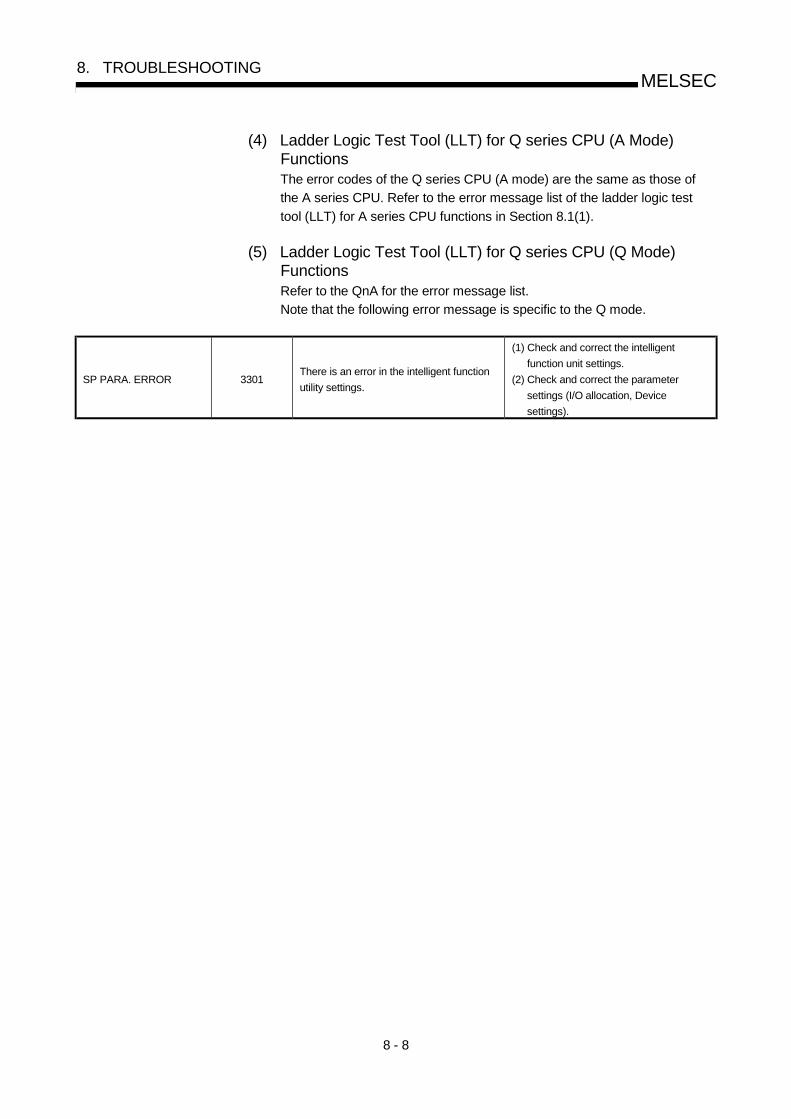
8 - 8
MELSEC8. TROUBLESHOOTING
(4) Ladder Logic Test Tool (LLT) for Q series CPU (A Mode)FunctionsThe error codes of the Q series CPU (A mode) are the same as those of
the A series CPU. Refer to the error message list of the ladder logic test
tool (LLT) for A series CPU functions in Section 8.1(1).
(5) Ladder Logic Test Tool (LLT) for Q series CPU (Q Mode)FunctionsRefer to the QnA for the error message list.
Note that the following error message is specific to the Q mode.
SP PARA. ERROR 3301There is an error in the intelligent function
utility settings.
(1) Check and correct the intelligent
function unit settings.
(2) Check and correct the parameter
settings (I/O allocation, Device
settings).

Appendix - 1
MELSECAPPENDICES
App.
APPENDICES
Appendix 1 List of Supported Devices
The ladder logic test tool (LLT) supports the devices for an A series CPU, QnA series
CPU, Q series CPU, and FXCPU.
(Non-supported devices are reserved as devices for reading and writing only.)
For the motion controller CPU, refer to the compatible devices of the A series CPU. For
the compatible CPU, refer to Section 2.3.
The devices supported by the ladder logic test tool (LLT) are listed in Appendix Table
1.1 to Appendix Table 1.15.
Appendix 1.1 The A series CPU function ladder logic test tool (LLT)
(1) Device list
Appendix Table 1.1 List of Devices Supported by the Ladder Logic Test Tool (LLT)Device range (points)
Device A0J2H
A1FX
A1N
A1S
A1SJ
A2C
A2CJ
A2S
A2N(S1)
A3N
A1SH
A1SJH
A2SH
A2A(S1) A3A
A2U(S1)
A2US(S1)
A2USH-S1
A3U
A4U
Input (X) 1X0 to X1FF
(512 points)
X0 to XFF
(256 points)
X00 to X1FF
(512 points)
X00 to X3FF
(1024 points)
X0 to X7FF
(2048 points)
X00 to X3FF
(1024 points)
X00 to X7FF
(2048 points)
X00 to X1FFF
(8192 points)
Output (Y) 1Y0 to Y1FF
(512 points)
Y0 to YFF
(256 points)
Y00 to Y1FF
(512 points)
Y00 to Y3FF
(1024 points)
Y0 to Y7FF
(2048 points)
Y00 to Y3FF
(1024 points)
Y00 to Y7FF
(2048 points)
Y00 to Y1FFF
(8192 points)
Internal relay (M) M0 to M2047 (2048 points) M0 to M8191 (8192 points)
Special relay (M) M9000 to M9255 (256 points)
Link relay (B) B0 to B3FF (1024 points) B0 to BFFF (4096 points)B0 to B1FFF
(8192 points)
Bit
devi
ce
Annunciator (F) F0 to F255 (256 points) F0 to F2047 (2048 points)
Timer (T) T0 to T255 (256 points) T0 to T2047 (2048 points)
Counter (C) C0 to C255 (256 points) C0 to C1023 (1024 points)
Data register (D) D0 to D1023 (1024 points) D0 to D6143 (6144 points)D0 to D8191
(8192 points)
Special register (D) D9000 to D9255 (256 points)
Link register (W) W0 to W3FFF (1024 points) W0 to WFFF (8192 points)W0 to W1FFF
(8192 points)
File register (R) R0 to R8191 (8192 points)
Extension file register Block 1 to 64 (8k points) 2
Accumulator (A) A0, A1 (2 points)
Wor
d de
vice
Index register (Z, V) Z, V (2 points) Z, Z1 to Z6, V, V1 to V6 (14 points)
Nesting (N) N0 to N7 (8 points)
Pointer (P) P0 to P255 (256 points)
Decimal constant (K) K-2147483648 to K2147483647
Hexadecimal constant (H) H0 to HFFFFFFFF
Character string constant "ABC", "123"
1 : Remote I/O is included.
2 : In the SW2D5 -GPPW, the data of file register can be written in the block No. 1 through 48 only.
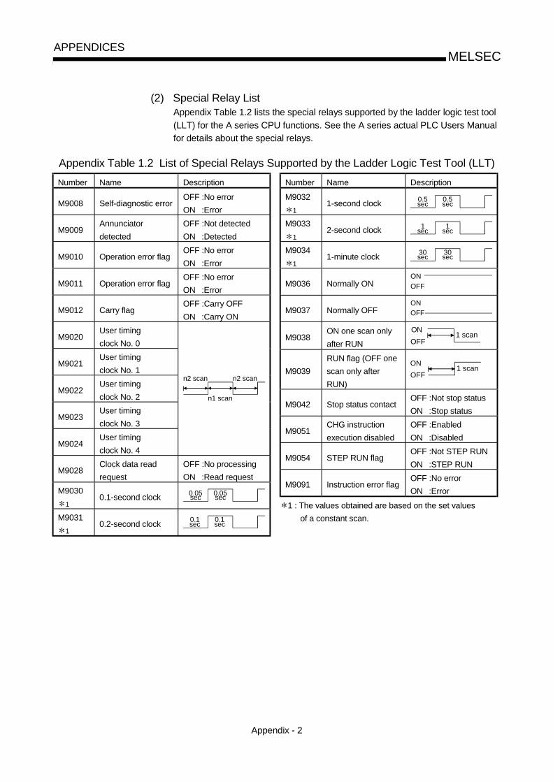
Appendix - 2
MELSECAPPENDICES
(2) Special Relay ListAppendix Table 1.2 lists the special relays supported by the ladder logic test tool
(LLT) for the A series CPU functions. See the A series actual PLC Users Manual
for details about the special relays.
Appendix Table 1.2 List of Special Relays Supported by the Ladder Logic Test Tool (LLT)
Number Name Description
M9008 Self-diagnostic errorOFF :No error
ON :Error
M9009Annunciator
detected
OFF :Not detected
ON :Detected
M9010 Operation error flagOFF :No error
ON :Error
M9011 Operation error flagOFF :No error
ON :Error
M9012 Carry flagOFF :Carry OFF
ON :Carry ON
M9020User timing
clock No. 0
M9021User timing
clock No. 1
M9022User timing
clock No. 2
M9023User timing
clock No. 3
M9024User timing
clock No. 4
n2 scan n2 scan
n1 scan
M9028Clock data read
request
OFF :No processing
ON :Read request
M9030
10.1-second clock
0.05sec
0.05sec
M9031
10.2-second clock
0.1 sec
0.1 sec
Number Name Description
M9032
11-second clock
0.5sec
0.5sec
M9033
12-second clock 1
sec1
sec
M9034
11-minute clock
30sec
30sec
M9036 Normally ONON
OFF
M9037 Normally OFFON
OFF
M9038ON one scan only
after RUN
ON
OFF1 scan
M9039
RUN flag (OFF one
scan only after
RUN)
ON
OFF1 scan
M9042 Stop status contactOFF :Not stop status
ON :Stop status
M9051CHG instruction
execution disabled
OFF :Enabled
ON :Disabled
M9054 STEP RUN flagOFF :Not STEP RUN
ON :STEP RUN
M9091 Instruction error flagOFF :No error
ON :Error
1 : The values obtained are based on the set values
of a constant scan.

Appendix - 3
MELSECAPPENDICES
(3) Special Register ListAppendix Table 1.3 lists the special registers supported by the ladder logic test
tool (LLT) for the A series CPU functions. See the A series actual PLC Users
Manual for details about the special registers.
Appendix Table 1.3 List of Special Registers Supported by the Ladder Logic Test Tool (LLT)
Number Name Description
D9008 Self-diagnostic errorSelf-diagnostic error
number
D9009Annunciator
detected
F number from
external breakdown
D9010 Error step
Step number where
operation error
occurred
D9011 Error step
Step number where
operation error
occurred
D9015CPU operation
statusCPU operation status
D9016 Program number
Saves the BIN value
of the executing
sequence program.
D9017
2Scan time
Minimum scan time
(10 ms units)
D9018
2Scan time
Scan time
(10ms units)
D9019
2Maximum scan time
Maximum scan time
(10ms units)
D9020
3Constant scan
Constant scan time
(user settable in 10
ms units)
D9021
2Scan time
Scan time
(1 ms units)
D9022
11-second counter
Number of counts in
1-second intervals
D9025 Clock dataClock data
(year, month)
Number Name Description
D9026 Clock data Clock data (day, hour)
D9027 Clock dataClock data
(minute, second)
D9028 Clock dataClock data
( , day of week)
D9035Extension file
registerBlock No. used
D9036
D9037
Designates device
number of
extension file
register.
Device number for
direct access of each
extension file registers
device.
D9091Detailed error
number
Self-diagnosis
detailed error number
D9124
Quantity of
annunciators
detected
Quantity of
annunciators detected
D9125
D9126
D9127
D9128
D9129
D9130
D9131
D9132
Number of detected
annunciators
Number of detected
annunciators
1 : Value derived from the constant scan set value.
2 : Value equal to all constant scan set values. Default
value is 100 ms.
3 : The set constant time becomes the time for one scan.

Appendix - 4
MELSECAPPENDICES
Appendix 1.2 The QnA series CPU Function Ladder Logic Test Tool (LLT)
(1) Device list
Appendix Table 1.4 List of Devices Supported by the Ladder Logic Test Tool (LLT)
Device Name Device Range (Points) Remarks
Input (X) X0 to X1FFF (8192 points) Actual inputs are disabled.
Output (Y) Y0 to Y1FFF (8192 points) Actual outputs are disabled.
Internal relay (M) M0 to M8191 (8191 points)
Latch relay (L) L0 to L8191 (8191 points)
Annunciator (F) F0 to F2047 (2048 points)
Edge relay (V) V0 to V2047 (2048 points)
Link special relay (SB) SB0 to SB7FF (2048 points)
Link relay (B) B0 to B1FFF (8192 points)
Special relay (SM) SM0 to SM2047 (2048 points)See (b) Special Relay List for details
about the special relays supported.
Function input (FX) FX0 to FX4 (5 points)
Bit
devi
ce
Function output (FY) FY0 to FY4 (5 points)
Data register (D) D0 to D12287 (12288 points)
Special register (SD) SD0 to SD2047 (2048 points)
See (c) Special Register List for
details about the special registered
supported.
Link register (W) W0 to W1FFF (8192 points)
Link special register (SW) SW0 to SW7FF (2048 points)
Timer (T) T0 to T2047 (2048 points)
Retentive timer (ST) (ST0 to ST2047) (0 points)
Counter (C) C0 to C1023 (1024 points)
Function register (FD) FD0 to FD4 (5 points)
File register (R) R0 to R1042431 (1042432 points)
Buffer register (Un\G) Un\G0 to Un\G16383 (16384 points)I/O assignments must be set for the
parameters.
Wor
d de
vice
Index register (Z) Z0 to Z15 (16 points)
Nesting (N) N0 to N14 (15 points)
Pointer (P) P0 to P4095 (4096 points)
Decimal constant (K) K-2147483648 to K2147483647
Hexadecimal constant (H) H0 to HFFFFFFFF
Real number constant E±1.17549-38 to E±3.40282+38
Character string constant "ABC", "123"Maximum 16 characters per
instruction.

Appendix - 5
MELSECAPPENDICES
(2) Special Relay ListAppendix Table 1.5 lists the special relays supported by the ladder logic test tool
(LLT) for the QnA series CPU functions. See the QnA series actual PLC Users
Manual for details about the special relays.
Appendix Table 1.5 List of Special Relays Supported by the Ladder Logic Test Tool (LLT)
Number Name Description
SM0 Diagnostic errorOFF :No error
ON :Error
SM1Self-diagnostic
error
OFF :No self-diagno-
stic error
ON :Self-diagnostic
error
SM5Error common
information
OFF :No error
common
information
ON :Error common
information
SM16Error individual
information
OFF :No error
individual
information
ON :Error individual
information
SM50 Error resetOFF ON :Error
reset
SM56 Operation errorOFF :Normal
ON :Operation error
SM62Annunciator
detected
OFF :Not detected
ON :Detected
SM203 STOP contacts STOP status
SM205STEP-RUN
contactsSTEP-RUN status
SM213Clock data read
request
OFF :No processing
ON :Read request
SM400 Normally ONON
OFF
SM401 Normally OFFON
OFF
SM402ON one scan only
after RUN
ON
OFF1 scan
SM403OFF one scan only
after RUN
ON
OFF1 scan
SM404ON one scan only
after RUN
ON
OFF1 scan
Number Name Description
SM405OFF one scan only
after RUN
ON
OFF1 scan
SM410
10.1-second clock
0.05 sec
0.05 sec
SM411
10.2-second clock
0.1 sec
0.1 sec
SM412
11-second clock 0.5
sec0.5sec
SM413
12-second clock
1sec
1sec
SM414
12n-second clock
nsec
nsec
SM420User timing
clock No.0
SM421User timing
clock No.1
SM422User timing
clock No.2
SM423User timing
clock No.3
SM424User timing
clock No.4
SM430User timing
clock No.5
SM431User timing
clock No.6
SM432User timing
clock No.7
SM433User timing
clock No.8
SM434User timing
clock No.9
n2 scan n2 scan
n1 scan
SM510Low-speed prog-
ram execution flag
OFF :Complete or no
execution
ON :Executing

Appendix - 6
MELSECAPPENDICES
Appendix Table 1.5 List of Special Relays Supported by the Ladder Logic Test Tool (LLT) (cont.)
Number Name Description
SM640 Use file register
OFF :File registers not
used
ON :File registers
used
SM700 Carry flagOFF :Carry OFF
ON :Carry ON
SM703 Sort orderOFF :Ascending
ON :Descending
SM704 Block comparison
OFF :Some do not
match
ON :All match
SM715 EI flagOFF :DI
ON :EI
SM776
Local device
enable/disable
setting at CALL time
OFF :Local device
disable
ON :Local device
enable
SM1008 Self-diagnostic errorOFF :No error
ON :Error
SM1009Annunciator
detected
OFF :Not detected
ON :Detected
SM1010 Operation errorOFF :Normal
ON :Operation error
SM1020User timing
clock No.0
SM1021User timing
clock No.1
SM1022User timing
clock No.2
SM1023User timing
clock No.3
SM1024User timing
clock No.4
n2 scan n2 scan
n1 scan
Number Name Description
SM1030 0.1-second clock0.05 sec
0.05 sec
SM1031 0.2-second clock 0.1 sec
0.1 sec
SM1032 1-second clock 0.5sec
0.5sec
SM1033 2-second clock 1sec
1sec
SM1034 2n-second clock nsec
nsec
SM1036 Normally ONON
OFF
SM1037 Normally OFFON
OFF
SM1038ON one scan only
after RUN
ON
OFF1 scan
SM1039OFF one scan only
after RUN
ON
OFF1 scan
SM1042 Stop status contactOFF :Not stop status
ON :Stop status
SM1054 STEP RUN flagON :STEP RUN
OFF :Not STEP RUN

Appendix - 7
MELSECAPPENDICES
(3) Special Register ListAppendix Table 1.6 lists the special registers supported by the ladder logic test
tool (LLT) for the QnA series CPU functions. See the QnA series actual PLC
Users Manual for details about the special registers.
Appendix table 1.6 List of Special Registers Supported by the Ladder Logic Test Tool (LLT)
Number Name Description
SD0 Diagnostic errorDiagnostic errornumber
SD1
SD2
SD3
Time the diagnosticerror occurred
Time the diagnosticerror occurred
SD4Error informationclass
Error information classcode
SD5
SD6
SD7
SD8
SD9
SD10
SD11
SD12
SD13
SD14
SD15
Error commoninformation
Error commoninformation
SD16
SD17
SD18
SD19
SD20
SD21
SD22
SD23
SD24
SD25
SD26
Error independentinformation
Error independentinformation
SD50 Error reset Reset error number
SD62 Annunciator No. Annunciator No.
SD63Annunciatorquantity
Annunciator quantity
SD64
SD65
SD66
SD67
SD68
SD69
Annunciatordetected numbertable
Annunciator detectednumber
Number Name Description
SD70
SD71
SD72
SD73
SD74
SD75
SD76
SD77
SD78
SD79
Annunciatordetected numbertable
Annunciator detectednumber
SD200 Switch status CPU switch status
SD203CPU operatingstatus
CPU operating status3
SD210 Clock dataClock data(year, month)
SD211 Clock dataClock data(day, hour)
SD212 Clock dataClock data(minute, second)
SD213 Clock dataClock data( , day of week)
SD290No. of X pointsassigned
SD291No. of Y pointsassigned
SD292No. of M pointsassigned
SD293No. of L pointsassigned
SD294No. of B pointsassigned
SD295No. of F pointsassigned
SD296No. of SB pointsassigned
SD297No. of V pointsassigned
SD298No. of S pointsassigned
SD299
Device assignment
No. of T pointsassigned
1 : Value derived from the constant scan setting value and number of scans.
2 : Values equal to all constant scan setting values.3 : SD203 supports the CPU operation status only.
STOP/PAUSE cause is fixed at 0.

Appendix - 8
MELSECAPPENDICES
Appendix Table 1.6 List of Special Registers Supported by the Ladder Logic Test Tool (LLT) (cont.)
Number Name Description
SD300No. of ST points
assigned
SD301No. of C points
assigned
SD302No. of D points
assigned
SD303No. of W points
assigned
SD304
Device assignment
No. of SW points
assigned
SD412
11-second counter
Number of counts in
1-second intervals
SD414
1
2n-second clock
setting2n-second clock units
SD420 Scan counterNumber of scans
counted
SD430Low-speed scan
counter
Number of scans
counted
SD500Executed program
number
Program execution
type.
SD510Low-speed program
number
Current low-speed
execution file name
SD520
2
Present scan time
(1 ms units)
SD521
2
Present scan timePresent scan time
(1 µs units)
SD522
2
Initial scan time
(1 ms units)
SD523
2
Initial scan timeInitial scan time
(1 µs units)
SD524
2
Minimum scan time
(1 ms units)
SD525
2
Minimum scan timeMinimum scan time
(1 µs units)
SD526
2
Maximum scan time
(1 ms units)
SD527
2
Maximum scan timeMaximum scan time
(1 µs units)
SD528
2
Current scan time
(1 ms units)
SD529
2
Current low-speed
scan time Current scan time
(1 µs units)
Number Name Description
SD532
2
Minimum low-speed
scan time (1 ms units)
SD533
2
Minimum low-speed
scan time Minimum scan time
(1 µs units)
SD534
2
Maximum scan time
(1 ms units)
SD535
2
Maximum low-
speed scan time Maximum scan time
(1 µs units)
SD647File register
capacityFile register capacity
SD648File register block
number
File register block
number
SD1008 Self-diagnostic errorSelf-diagnostic error
number
SD1009 Annunciator No. Annunciator No.
SD1015CPU operation
statusCPU operation status
SD1017
2Scan time
Minimum scan time
(10 ms units)
SD1018
2Scan time
Scan time
(10 ms units)
SD1019
2Scan time
Maximum scan time
(10 ms units)
SD1021
2Scan time
Scan time
(1 ms units)
SD1022
21-second counter
Number of counts of
1-second units
SD1035Extension file
registerUsed block number
SD1124Number of annun-
ciators detected
Number of annun-
ciators detected
SD1125
SD1126
SD1127
SD1128
SD1129
SD1130
SD1131
SD1132
Number of annun-
ciators detected
Number of annun-
ciators detected
1 : Value derived from the constant scan setting value and
number of scans.
2 : Values equal to all constant scan setting values.
3 : SD203 supports the CPU operation status only.
STOP/PAUSE cause is fixed at 0.

Appendix - 9
MELSECAPPENDICES
POINTSpecial relays/registers that have contents different from those of Q4ACPU will
operate by the contents of special relays/registers of Q4ACPU.
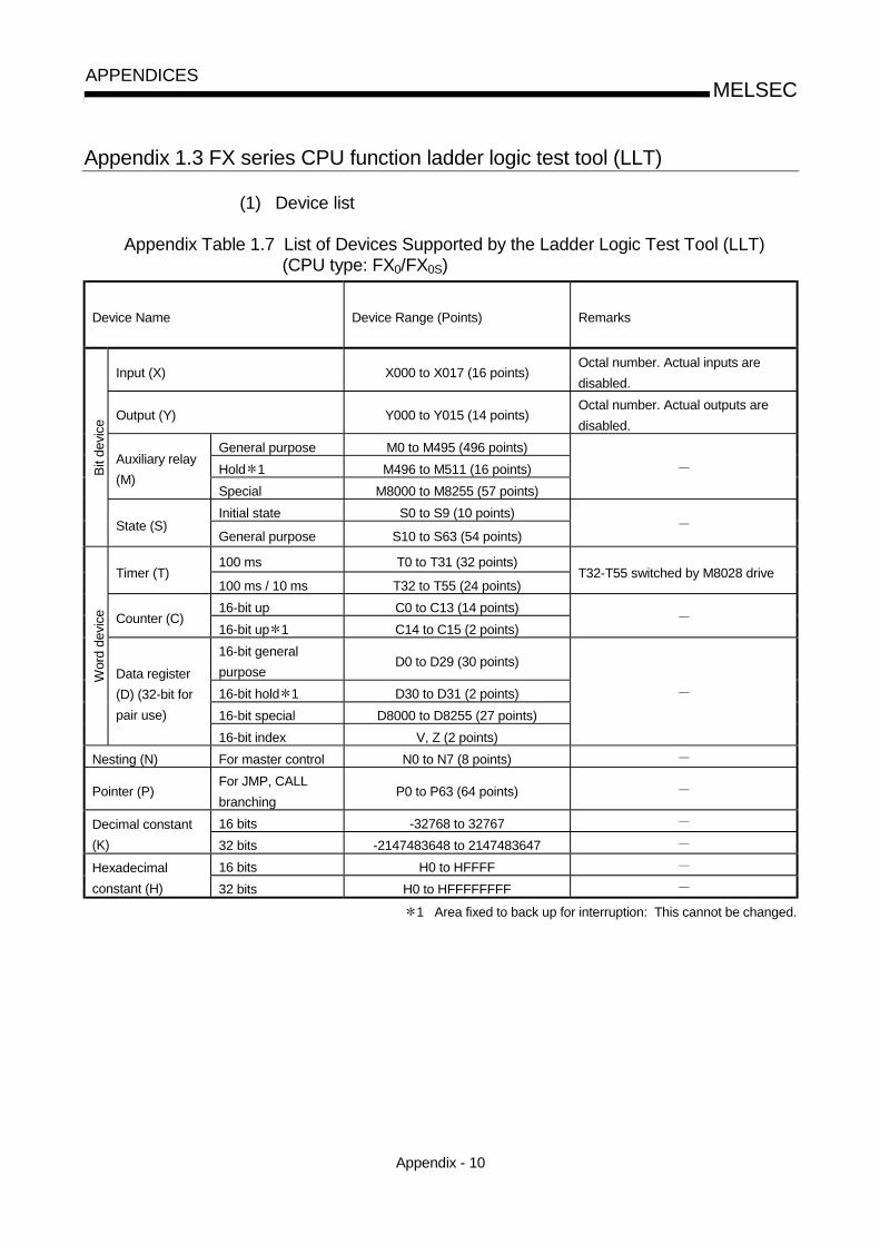
Appendix - 10
MELSECAPPENDICES
Appendix 1.3 FX series CPU function ladder logic test tool (LLT)
(1) Device list
Appendix Table 1.7 List of Devices Supported by the Ladder Logic Test Tool (LLT) (CPU type: FX0/FX0S)
Device Name Device Range (Points) Remarks
Input (X) X000 to X017 (16 points)Octal number. Actual inputs are
disabled.
Output (Y) Y000 to Y015 (14 points)Octal number. Actual outputs are
disabled.
General purpose M0 to M495 (496 points)
Hold 1 M496 to M511 (16 points)Auxiliary relay
(M)Special M8000 to M8255 (57 points)
Initial state S0 to S9 (10 points)
Bit
devi
ce
State (S)General purpose S10 to S63 (54 points)
100 ms T0 to T31 (32 points)Timer (T)
100 ms / 10 ms T32 to T55 (24 points)T32-T55 switched by M8028 drive
16-bit up C0 to C13 (14 points)Counter (C)
16-bit up 1 C14 to C15 (2 points)
16-bit general
purposeD0 to D29 (30 points)
16-bit hold 1 D30 to D31 (2 points)
16-bit special D8000 to D8255 (27 points)
Wor
d de
vice
Data register
(D) (32-bit for
pair use)
16-bit index V, Z (2 points)
Nesting (N) For master control N0 to N7 (8 points)
Pointer (P)For JMP, CALL
branchingP0 to P63 (64 points)
16 bits -32768 to 32767Decimal constant
(K) 32 bits -2147483648 to 2147483647
16 bits H0 to HFFFFHexadecimal
constant (H) 32 bits H0 to HFFFFFFFF
1 Area fixed to back up for interruption: This cannot be changed.

Appendix - 11
MELSECAPPENDICES
Appendix Table 1.8 List of Devices Supported by the Ladder Logic Test Tool (LLT) (CPU type: FX0N)
Device Name Device Range (Points) Remarks
Input (X)
Total number of
points with
expansion
X000 to X177 (128 points)Octal number. Actual inputs are
disabled.
output (Y)
Total number of
points with
expansion
Y000 to Y177 (128 points)Octal number. Actual outputs are
disabled.
general purpose M0 to M383 (384 points)
Hold 1 M384 to M511 (128 points)Auxiliary relay
(M)Special M8000 to M8255 (67 points)
Initial state 1 S0 to S9 (10 points)
Bit
devi
ce
State (S)Hold 1 S10 to S127 (118 points)
100 ms T0 to T31 (32 points)
100 ms / 10 ms T32 to T62 (31 points)T32-T62 switched by M8028 drive
Timer (T)
1 ms T63 (1 point)
16 bit up C0 to C15 (16 points)Counter (C)
16bit up 1 C16 to C31 (16 points)
16-bit general
purposeD0 to D127 (128 points)
16-bit hold 1 D128 to D255 (128 points)
16-bit special D8000 to D8255 (106 points)
File 1 D1000 to D2499 (1500 points)
Wor
d de
vice
Data register
(D) (32-bit for
pair use)
16-bit index V, Z (2 points)
Nesting (N) For master control N0 to N7 (8 points)
Pointer (P)For JMP, CALL
branchingP0 to P63 (64 points)
16 bits -32768 to 32767Decimal constant
(K) 32 bits -2147483648 to 2147483647
16 bits H0 to HFFFFHexadecimal
constant (H) 32 bits H0 to HFFFFFFFF
1 Area fixed to back up for interruption: This cannot be changed.
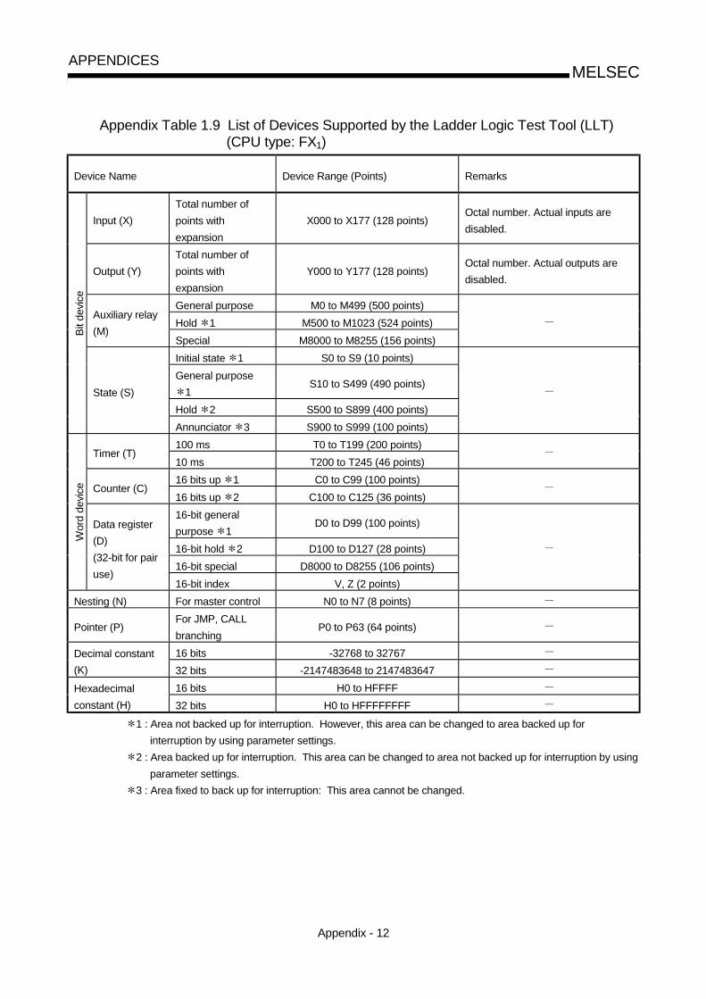
Appendix - 12
MELSECAPPENDICES
Appendix Table 1.9 List of Devices Supported by the Ladder Logic Test Tool (LLT) (CPU type: FX1)
Device Name Device Range (Points) Remarks
Input (X)
Total number of
points with
expansion
X000 to X177 (128 points)Octal number. Actual inputs are
disabled.
Output (Y)
Total number of
points with
expansion
Y000 to Y177 (128 points)Octal number. Actual outputs are
disabled.
General purpose M0 to M499 (500 points)
Hold 1 M500 to M1023 (524 points)Auxiliary relay
(M)Special M8000 to M8255 (156 points)
Initial state 1 S0 to S9 (10 points)
General purpose
1S10 to S499 (490 points)
Hold 2 S500 to S899 (400 points)
Bit
devi
ce
State (S)
Annunciator 3 S900 to S999 (100 points)
100 ms T0 to T199 (200 points)Timer (T)
10 ms T200 to T245 (46 points)
16 bits up 1 C0 to C99 (100 points)Counter (C)
16 bits up 2 C100 to C125 (36 points)
16-bit general
purpose 1D0 to D99 (100 points)
16-bit hold 2 D100 to D127 (28 points)
16-bit special D8000 to D8255 (106 points)
Wor
d de
vice
Data register
(D)
(32-bit for pair
use)16-bit index V, Z (2 points)
Nesting (N) For master control N0 to N7 (8 points)
Pointer (P)For JMP, CALL
branchingP0 to P63 (64 points)
16 bits -32768 to 32767Decimal constant
(K) 32 bits -2147483648 to 2147483647
16 bits H0 to HFFFFHexadecimal
constant (H) 32 bits H0 to HFFFFFFFF
1 : Area not backed up for interruption. However, this area can be changed to area backed up for
interruption by using parameter settings.
2 : Area backed up for interruption. This area can be changed to area not backed up for interruption by using
parameter settings.
3 : Area fixed to back up for interruption: This area cannot be changed.

Appendix - 13
MELSECAPPENDICES
Appendix Table 1.10 List of Devices Supported by the Ladder Logic Test Tool (LLT) (CPU type: FX2/FX2C)
Device Name Device Range (Points) Remarks
Input (X)Total number ofpoints withexpansion
X000 to X377 (256 points)Octal number. Actual inputs aredisabled.
Output (Y)Total number ofpoints withexpansion
Y000 to Y377 (256 points)Octal number. Actual outputs aredisabled.
General purpose1
M0 to M499 (500 points)
Hold 2 M500 to M1023 (524 points)
Hold 3 M1024 to M1535 (512 points)
Auxiliary relay(M)
Special M8000 to M8255 (156 points)
Initial state 1 S0 to S9 (10 points)
General purpose1
S10 to S499 (490 points)
Hold 2 S500 to S899 (400 points)
Bit
devi
ce
State (S)
Annunciator 3 S900 to S999 (100 points)
100 ms T0 to T199 (200 points)
10 ms T200 to T245 (46 points)
1 ms retentive 3 T246 to T249 (4 points)Timer (T)
100 ms retentive3
T250 to T255 (6 points)
16-bit up 1 C0 to C99 (100 points)
16-bit up 2 C100 to C199 (100 points)
32-bit bi-directional1
C200 to C219 (20 points)Counter (C)
32-bit bi-directional2
C220 to C234 (15 points)
16-bit generalpurpose 1
D0 to D199 (200 points)
16-bit hold 2 D200 to D511 (312 points)
16-bit hold 3 D512 to D999 (488 points)
16-bit special D8000 to D8255 (106 points)
File 3 D1000 to D2999 (2000 points)
RAM file D6000 to D7999 (2000 points)
Wor
d de
vice
Data register(D)(32-bit for pairuse)
16-bit index V, Z (2 points)
Nesting (N) For master control N0 to N7 (8 points)
Pointer (P)For JMP, CALLbranching
P0 to P127 (128 points)
16 bits -32768 to 32767Decimal constant(K) 32 bits -2147483648 to 2147483647
16 bits H0 to HFFFFHexadecimalconstant (H) 32 bit H0 to HFFFFFFFF
1 : Area not backed up for interruption. However, this area can be changed to area backed up for
interruption by using parameter settings.
2 : Area backed up for interruption. This area can be changed to area not backed up for interruption by using
parameter settings.
3 : Area fixed to back up for interruption: This area cannot be changed.

Appendix - 14
MELSECAPPENDICES
Appendix Table 1.11 List of Devices Supported by the Ladder Logic Test Tool (LLT) (CPU type: FX1S)
Device Name Device Range (Points) Remarks
Input (X)
Total number of
points with
expansion
X000 to X017 (16 points)Octal number. Actual inputs are
disabled.
output (Y)
Total number of
points with
expansion
Y000 to Y015 (14 points)Octal number. Actual outputs are
disabled.
general purpose M0 to M383 (384 points)
Hold 1 M384 to M511 (128 points)Auxiliary relay
(M)Special M8000 to M8255 (256 points)
Initial state 1 S0 to S9 (10 points)
Bit
devi
ce
State (S)Hold 1 S0 to S127 (128 points)
100 ms T0 to T31 (32 points)
100 ms / 10 ms T32 to T62 (31 points)T32-T62 switched by M8028 drive
Timer (T)
1 ms retentive 1 T63 (1 point)
16 bit up C0 to C15 (16 points)Counter (C)
16bit up 1 C16 to C31 (16 points)
16-bit general
purposeD0 to D127 (128 points)
16-bit hold 1 D128 to D255 (128 points)
16-bit special D8000 to D8255 (256 points)
File 1 D1000 to D2499 (1500 points)
Wor
d de
vice
Data register
(D) (32-bit for
pair use)
16-bit index V0 to V7, Z0 to Z7 (16 points)
Nesting (N) For master control N0 to N7 (8 points)
Pointer (P)For JMP, CALL
branchingP0 to P63 (64 points)
16 bits -32768 to 32767Decimal constant
(K) 32 bits -2147483648 to 2147483647
16 bits H0 to HFFFFHexadecimal
constant (H) 32 bits H0 to HFFFFFFFF
1 Area fixed to back up for interruption: This cannot be changed.
Appendix Table 1.12 List of Devices Supported by the Ladder Logic Test Tool (LLT)
(CPU type: FX1N)
Devices other than high-speed counter are supported:
Refer to handy manual attached to the sequencer for the range of FX1N series
devices.

Appendix - 15
MELSECAPPENDICES
Appendix Table 1.13 List of Devices Supported by the Ladder Logic Test Tool (LLT) (CPU type: FX2N/FX22NC)
Device Name Device Range (Points) Remarks
Input (X)Total number ofpoints withexpansion
X000 to X377 (256 points)Octal number. Actual inputs aredisabled.
Output (Y)Total number ofpoints withexpansion
Y000 to Y377 (256 points)Octal number. Actual outputs aredisabled.
General purpose1
M0 to M499 (500 points)
Hold 2 M500 to M1023 (524 points)
Hold 3 M1024 to M3071 (2048 points)
Auxiliary relay(M)
Special M8000 to M8255 (156 points)
Initial state 1 S0 to S9 (10 points)
General purpose1
S10 to S499 (490 points)
Hold 2 S500 to S899 (400 points)
Bit
devi
ce
State (S)
Annunciator 3 S900 to S999 (100 points)
100 ms T0 to T199 (200 points)
10 ms T200 to T245 (46 points)
1 ms retentive 3 T246 to T249 (4 points)Timer (T)
100 ms retentive3
T250 to T255 (6 points)
16-bit up 1 C0 to C99 (100 points)
16-bit up 2 C100 to C199 (100 points)
32-bit bi-directional1
C200 to C219 (20 points)Counter (C)
32-bit bi-directional2
C220 to C234 (15 points)
16-bit generalpurpose 1
D0 to D199 (200 points)
16-bit hold 2 D200 to D511 (312 points)
16-bit hold 3 D512 to D7999 (7488 points)
16-bit special D8000 to D8255 (106 points)
Wor
d de
vice
Data register(D)(32-bit for pairuse)
16-bit index V0 to V7, Z0 to Z7 (16 points)
Nesting (N) For master control N0 to N7 (8 points)
Pointer (P)For JMP, CALLbranching
P0 to P127 (128 points)
16 bits -32768 to 32767Decimal constant(K) 32 bits -2147483648 to 2147483647
16 bits H0 to HFFFFHexadecimalconstant (H) 32 bit H0 to HFFFFFFFF
1 : Area not backed up for interruption. However, this area can be changed to area backed up for
interruption by using parameter settings.
2 : Area backed up for interruption. This area can be changed to area not backed up for interruption by using
parameter settings.
3 : Area fixed to back up for interruption: This area cannot be changed.

Appendix - 16
MELSECAPPENDICES
(2) Special Relay ListAppendix Table 1.14 lists the special relays supported by the ladder logic test
tool (LLT) for the FX series CPU functions. See the FX series actual PLC
Programming Manual for details about the special relays.
Appendix Table 1.14 List of Special Relays Supported by the Ladder Logic Test Tool (LLT)
No. Name DescriptionFX0,
FX0SFX0N FX1
FX2,
FX2CFX1S FX1N
FX2N,
FX2NC
M8000RUN monitor
N/O contact
OFF :STOP
ON :RUN
M8001RUN monitor
N/C contact
OFF :RUN
ON :STOP
M8002Initial pulse
N/O contactON one scan after RUN
M8003Initial pulse
N/C contactOFF one scan after RUN
M8004 Error occurredON if any of M8060 to
M8067 operates.
M8011 10 ms clock 5 ms5 ms
M8012 100 ms clock 50 ms50 ms
M8013 1 s clock 0.5 s0.5 s
M8014 1 min clock30 s30 s
M8018Internal real-time
clock detectedNormally ON
M8020 Zero ON if counting result is 0
M8021 BorrowON if counting result is less
than maximum minus value.
M8022 CarryON if counting result
increases a digit.
M8023Decimal-point
operation instruction
ON when floating decimal-
point instruction is executed.
M8024Designate BMOV
direction
ON :Write
OFF :Read
M8026RAMP mode
designation
ON :Hold output value
OFF :Reset output value
M8028Switch timer
instruction
OFF :100 ms base
ON :10 ms base
: This device or function is supported by the actual PLC.
: This device or function is not supported by the actual PLC.
: This device is supported by actual PLCs with a clock function.
For the ladder logic test tool (LLT), always ON regardless whether the actual PLC has a clock function.

Appendix - 17
MELSECAPPENDICES
Appendix Table 1.14 List of Special Relays Supported by the Ladder Logic Test Tool (LLT) (cont.)
No. Name DescriptionFX0,
FX0SFX0N FX1
FX2,
FX2CFX1S FX1N
FX2N,
FX2NC
M8029Instruction execution
complete
OFF :Executing
ON :Execution complete
M8031Non-hold memory all
clear instruction
OFF :Hold
ON :Clear
M8032Hold memory all clear
instruction
OFF :Hold
ON :Clear
M8033Memory hold stop
instruction
OFF :Clear
ON :Hold
M8034Disable all outputs
instruction
OFF :Output enabled
ON :Output OFF
M8038RAM file clear
instruction
OFF :Hold
ON :Clear
M8039Constant scan mode
designation
OFF :Normal scan
ON :Constant scan mode
M8040Disable transition
instruction
OFF :Transition enabled
ON :Transition disabled
M8041
Transition start
instruction
(for IST command)
OFF :Stop
ON :Transition start
M8042Start pulse instruction
(for IST command)
ON :IST command start
instruction
M8043
Home position return
complete instruction
(for IST command)
ON :IST command home
position return
instruction
M8044
Home position
condition
(for IST command)
ON :Home position
OFF :Home position return
not complete
M8045
All output reset
disabled
(for IST command)
ON :Reset disabled
OFF :Reset enabled
M8046 STL state operationON if any of S0 to S899
operates.
M8047 STL monitor enableON :D8040 to D8047
enabled
M8048 Annunciator operationON if any of S900 to S999
operates.
: This device or function is supported by the actual PLC.
: This device or function is not supported by the actual PLC.
: This device is supported by actual PLCs with a clock function.
For the ladder logic test tool (LLT), always ON regardless whether the actual PLC has a clock function.

Appendix - 18
MELSECAPPENDICES
Appendix Table 1.14 List of Special Relays Supported by the Ladder Logic Test Tool (LLT) (cont.)
No. Name DescriptionFX0,
FX0SFX0N FX1
FX2,
FX2CFX1S FX1N
FX2N,
FX2NC
M8049Annunciator enable
instruction
ON :D8049 enabled
OFF : D8049 enabled
M8067Operation error
occurred
ON :Operation error
OFF :No operation error
M8068 Operation error latch Holds M8067 status
M8074RAM file register
setting
ON :Use
OFF :Do not use
M8160XCH SWAP function
setting
ON :8-bit conversion
OFF :Normal mode
M8161 8-bit processing modeASC, ASCI, HEX
processing method
M8164
Change number of
FROM/TO instruction
transfer points
Transfer points switch
instruction
M8168SMOV HEX data
handling functionsDigit shift in 4-bit unit
M8200Counting direction of
counter
ON :C200 down
OFF :C200 up
M8201Counting direction of
counter
ON :C201 down
OFF :C201 up
M8202Counting direction of
counter
ON :C202 down
OFF :C202 up
M8203Counting direction of
counter
ON :C203 down
OFF : C203 up
M8204Counting direction of
counter
ON :C204 down
OFF :C204 up
M8205Counting direction of
counter
ON :C205 down
OFF :C205 up
M8206Counting direction of
counter
ON :C206 down
OFF :C206 up
M8207Counting direction of
counter
ON :C207 down
OFF :C207 up
M8208Counting direction of
counter
ON :C208 down
OFF :C208 up
M8209Counting direction of
counter
ON :C209 down
OFF :C209 up
: This device or function is supported by the actual PLC.
: This device or function is not supported by the actual PLC.
: This device is supported by actual PLCs with a clock function.
For the ladder logic test tool (LLT), always ON regardless whether the actual PLC has a clock function.

Appendix - 19
MELSECAPPENDICES
Appendix Table 1.14 List of Special Relays Supported by the Ladder Logic Test Tool (LLT) (cont.)
No. Name DescriptionFX0,
FX0SFX0N FX1
FX2,
FX2CFX1S FX1N
FX2N,
FX2NC
M8210Counting direction of
counter
ON :C210 down
OFF :C210 up
M8211Counting direction of
counter
ON :C211 down
OFF :C211 up
M8212Counting direction of
counter
ON :C212 down
OFF :C212 up
M8213Counting direction of
counter
ON :C213 down
OFF :C213 up
M8214Counting direction of
counter
ON :C214 down
OFF :C214 up
M8215Counting direction of
counter
ON :C215 down
OFF :C215 up
M8216Counting direction of
counter
ON :C216 down
OFF :C216 up
M8217Counting direction of
counter
ON :C217 down
OFF :C217 up
M8218Counting direction of
counter
ON :C218 down
OFF :C218 up
M8219Counting direction of
counter
ON :C219 down
OFF :C219 up
M8220Counting direction of
counter
ON :C220 down
OFF :C220 up
M8221Counting direction of
counter
ON :C221 down
OFF :C221 up
M8222Counting direction of
counter
ON :C222 down
OFF :C222 up
M8223Counting direction of
counter
ON :C223 down
OFF :C223 up
M8224Counting direction of
counter
ON :C224 down
OFF :C224 up
M8225Counting direction of
counter
ON :C225 down
OFF :C225 up
M8226Counting direction of
counter
ON :C226 down
OFF :C226 up
M8227Counting direction of
counter
ON :C227 down
OFF :C227 up
: This device or function is supported by the actual PLC.
: This device or function is not supported by the actual PLC.
: This device is supported by actual PLCs with a clock function.
For the ladder logic test tool (LLT), always ON regardless whether the actual PLC has a clock function.

Appendix - 20
MELSECAPPENDICES
Appendix Table 1.14 List of Special Relays Supported by the Ladder Logic Test Tool (LLT) (cont.)
No. Name DescriptionFX0,
FX0SFX0N FX1
FX2,
FX2CFX1S FX1N
FX2N,
FX2NC
M8228Counting direction of
counter
ON :C228 down
OFF :C228 up
M8229Counting direction of
counter
ON :C229 down
OFF :C229 up
M8230Counting direction of
counter
ON :C230 down
OFF :C230 up
M8231Counting direction of
counter
ON :C231 down
OFF :C231 up
M8232Counting direction of
counter
ON :C232 down
OFF :C232 up
M8233Counting direction of
counter
ON :C233 down
OFF :C233 up
M8234Counting direction of
counter
ON :C234 down
OFF :C234 up
:This device or function is supported by the actual PLC.
:This device or function is not supported by the actual PLC.
:This device is supported by actual PLCs with a clock function.
For the ladder logic test tool (LLT), always ON regardless whether the actual PLC has a clock function.
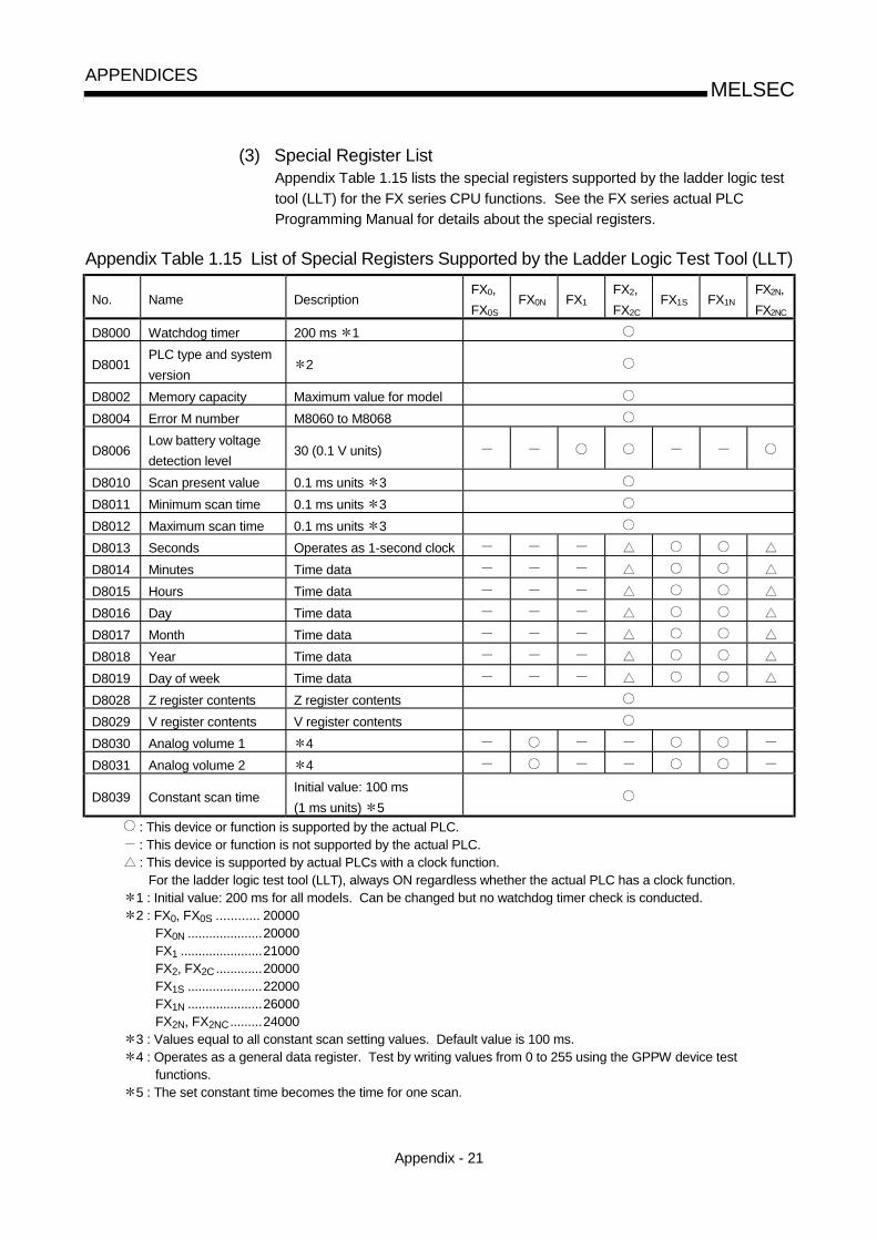
Appendix - 21
MELSECAPPENDICES
(3) Special Register ListAppendix Table 1.15 lists the special registers supported by the ladder logic test
tool (LLT) for the FX series CPU functions. See the FX series actual PLC
Programming Manual for details about the special registers.
Appendix Table 1.15 List of Special Registers Supported by the Ladder Logic Test Tool (LLT)
No. Name DescriptionFX0,
FX0SFX0N FX1
FX2,
FX2CFX1S FX1N
FX2N,
FX2NC
D8000 Watchdog timer 200 ms 1
D8001PLC type and system
version2
D8002 Memory capacity Maximum value for model
D8004 Error M number M8060 to M8068
D8006Low battery voltage
detection level30 (0.1 V units)
D8010 Scan present value 0.1 ms units 3
D8011 Minimum scan time 0.1 ms units 3
D8012 Maximum scan time 0.1 ms units 3
D8013 Seconds Operates as 1-second clock
D8014 Minutes Time data
D8015 Hours Time data
D8016 Day Time data
D8017 Month Time data
D8018 Year Time data
D8019 Day of week Time data
D8028 Z register contents Z register contents
D8029 V register contents V register contents
D8030 Analog volume 1 4
D8031 Analog volume 2 4
D8039 Constant scan timeInitial value: 100 ms
(1 ms units) 5
: This device or function is supported by the actual PLC. : This device or function is not supported by the actual PLC. : This device is supported by actual PLCs with a clock function.
For the ladder logic test tool (LLT), always ON regardless whether the actual PLC has a clock function.1 : Initial value: 200 ms for all models. Can be changed but no watchdog timer check is conducted.2 : FX0, FX0S ............ 20000
FX0N .....................20000FX1 .......................21000FX2, FX2C .............20000FX1S .....................22000FX1N .....................26000FX2N, FX2NC.........24000
3 : Values equal to all constant scan setting values. Default value is 100 ms.4 : Operates as a general data register. Test by writing values from 0 to 255 using the GPPW device test
functions.5 : The set constant time becomes the time for one scan.

Appendix - 22
MELSECAPPENDICES
Appendix Table 1.15 List of Special Registers Supported by the Ladder Logic Test Tool (LLT) (cont.)
No. Name DescriptionFX0,
FX0SFX0N FX1
FX2,
FX2CFX1S FX1N
FX2N,
FX2NC
D8040 ON state number 1 STL monitor contents
D8041 ON state number 2 STL monitor contents
D8042 ON state number 3 STL monitor contents
D8043 ON state number 4 STL monitor contents
D8044 ON state number 5 STL monitor contents
D8045 ON state number 6 STL monitor contents
D8046 ON state number 7 STL monitor contents
D8047 ON state number 8 STL monitor contents
D8049ON state minimum
numberSTL monitor contents
D8067Operation error code
numberError code number
D8068
Operation error
occurred step number
latch
Saves step number where
error occurred
D8069M8067 error occurred
step number
Step number where error
occurred
D8102 Memory capacity Maximum value for model
D8164
Designate number of
FROM/TO instruction
transfer points
Write transfer points
D8182 Z1 register contents Z1 register contents
D8183 V1 register contents V1 register contents
D8184 Z2 register contents Z2 register contents
D8185 V2 register contents V2 register contents
D8186 Z3 register contents Z3 register contents
D8187 V3 register contents V3 register contents
D8188 Z4 register contents Z4 register contents
D8189 V4 register contents V4 register contents
D8190 Z5 register contents Z5 register contents
D8191 V5 register contents V5 register contents
D8192 Z6 register contents Z6 register contents
D8193 V6 register contents V6 register contents
D8194 Z7 register contents Z7 register contents
D8195 V7 register contents V7 register contents
: This device or function is supported by the actual PLC.
: This device or function is not supported by the actual PLC.
: This device is supported by actual PLCs with a clock function.
For the ladder logic test tool (LLT), always ON regardless whether the actual PLC has a clock function.

Appendix - 23
MELSECAPPENDICES
1 : Initial value: 200 ms for all models. Can be changed but no watchdog timer check is conducted.2 : FX0, FX0S ............ 20000
FX0N .....................20000FX1 .......................21000FX2, FX2C .............20000FX1S .....................22000FX1N .....................26000FX2N, FX2NC.........24000
3 : Values equal to all constant scan setting values. Default value is 100 ms.4 : Operates as a general data register. Test by writing values from 0 to 255 using the GPPW device test
functions.
5 : The set constant time becomes the time for one scan.

Appendix - 24
MELSECAPPENDICES
Appendix 1.4 Ladder logic test tool (LLT) for Q series CPU (A mode) functions
(1) Device listSince the devices of the Q series CPU (A mode) are the same as those of theA4UCPU, refer to A4U in the List of Devices Supported by the Ladder Logic TestTool (LLT) in Appendix Table 1.1.
(2) Special relay listSince the special relays of the Q series CPU (A mode) are the same as those ofthe A series CPU, refer to the List of Special Relays Supported by the LadderLogic Test Tool (LLT) in Appendix Table 1.2.
(3) Special register listSince the special registers of the Q series CPU (A mode) are the same as thoseof the A series CPU, refer to the List of Special Registers Supported by theLadder Logic Test Tool (LLT) in Appendix Table 1.3.
Appendix 1.5 Ladder logic test tool (LLT) for Q series CPU (Q mode) functions
(1) Device list
Appendix Table 1.16 List of Devices Supported by the Ladder Logic Test Tool (LLT)
Device Device Range (Points) Setting Range Remarks
Input X0 to X1FFF (8192 Points) Fixed Actual inputs are disabled.
Output Y0 to Y1FFF (8192 Points) Fixed Actual outputs are disabled.
Internal relay M0 to M8191 (8192 Points) Changeable
Latch relay L0 to L8191 (8192 Points) Changeable
Annunciator F0 to F2047 (2048 Points) Changeable
Edge relay V0 to V2047 (2048 Points) Changeable
Step relay S0 to S511/Block Changeable Incompatible with SFC.
Link special relay SB0 to SB7FF (2048 Points) Changeable
Bit
devi
ce
Link relay B0 to B1FFF (8192 Points) Changeable
Timer T0 to T2047 (2048 Points) Changeable
No operation in real time.High-speed timer can be setin 0.1ms increments(in parameter).1ms increments inconventional LLT.
Retentive timer None (ST0 to-) Changeable
No operation in real time.High-speed retentive timercan be set in 0.1msincrements (in parameter).1ms increments inconventional LLT.
Counter C0 to C1023 (1024 Points) Changeable
Data register D0 to D12287 (12288 Points) Changeable
Link register W0 to W1FFF (8192 Points) Changeable
Wor
d de
vice
Link special register SW0 to SW7FF (2048 Points) Changeable

Appendix - 25
MELSECAPPENDICES
Appendix Table 1.16 List of Devices Supported by the Ladder Logic Test Tool (LLT) (cont.)
Name Device Range (Points) Setting Range Remarks
Function input FX0 to FXF (16 points) Fixed
Function output FY0 to FYF (16 points) Fixed
Bit
Special relay SM0 to SM2047 (2048 points) FixedCompatible with somefunctions.
Function register FD0 to FD4 (5 points) Fixed
Wor
d
Special register SD0 to SD2047 (2048 points) FixedCompatible with somefunctions.
Link input Jn\X0 to Jn\X1FFF (8192 points) FixedIncompatible with linkfunctions.
Link output Jn\Y0 to Jn\Y1FFF (8192 points) FixedIncompatible with linkfunctions.
Link relay Jn\B0 to JnB\3FFF (16384 points) FixedIncompatible with linkfunctions.
Bit
Link special relay Jn\SB0 to Jn\SB1FF (512 points) FixedIncompatible with linkfunctions.
Link register Jn\W0 to Jn\W3FFF (16384 points) FixedIncompatible with linkfunctions.
Wor
d
Link special register JnS\W0 to JnS\W1FF (512 points) FixedIncompatible with linkfunctions.
Buffer registerUn\G0 to Un\G65535
(65536 points)Fixed
16384 points in conventionalLLT.
Index register Z0 to Z15 (16 points) Fixed
Wor
d
File registerR0 to R18383 (18384 points)
ZR0 to ZR1042432(1042433 points)
Fixed
Nesting N0 to N14 (15 points) Fixed
Pointer P0 to P4095 (4096 points) Fixed
Interrupt pointer I0 to I47 (48 points) FixedIncompatible with interruptfunctions.
SFC block BL0 to BL319 (320 points) Fixed Incompatible with SFC.
Bit
SFC transition device TR0 to TR511 (512 points) Fixed Incompatible with SFC.
Network No. J1 to J255 (256 points) FixedIncompatible with linkfunctions.
I/O No. U0 to UFF (256 points) FixedIncompatible with link/specialmodules.
Decimal constant K-2147483648 to K2147483647 Fixed
Hexadecimal constant H0 to HFFFFFFFF Fixed
Real number constant E±1.17549-38 to E±3.40282+38 Fixed
Character string constant "ABC", "123"etc. FixedUp to 16 characters per
instruction
Bit CPU shared memory Un\GO to Un\GOFFF (4096 points) Fixed
Valid only multiple CPU
setting time

Appendix - 26
MELSECAPPENDICES
(2) Special Relay List
Appendix Table 1.17 List of Special Relays Supported by the Ladder Logic Test (LLT)
Device
NameRemarks
Device
NameRemarks
Device
NameRemarks
Device
NameRemarks
SM0 Diagnostic errorSM410
10.1 sec. clock SM620
Card B use flag
normally ONSM1022 User clock No. 2
SM1 Self-diagnostic errorSM411
10.2 sec. clock SM621
Card B protect flag
normally OFFSM1023 User clock No. 3
SM5Error common
information
SM412
11 sec. clock SM622
Drive 3 flag normally
ONSM1024 User clock No. 4
SM16Error individual
information
SM413
12 sec. clock SM623
Drive 4 flag normally
ONSM1030 0.1 sec. clock
SM50 Error resetSM414
12n sec. clock SM640 File register use SM1031 0.2 sec. clock
SM56 Operation errorSM415
12n millsec. clock SM700 Carry flag SM1032 1 sec. clock
SM62 Annunciator detection SM420 User clock No. 0 SM703 Sort order SM1033 2 sec. clock
SM203 STOP contact SM421 User clock No. 1 SM704 Block comparison SM1034 2n sec. clock
SM205 STEP-RUN contact SM422 User clock No. 2 SM715 EI flag SM1036 Normally ON
SM213Clock data read
requestSM423 User clock No. 3 SM722
BIN/DBIN error
processing switch-overSM1037 Normally OFF
SM400 Normally ON SM424 User clock No. 4 SM776
Local device
enable/disable setting
at CALL time
OFF :Local device
disable
ON :Local device
enable
SM1038ON only 1 scan after
RUN
SM401 Normally OFF SM430 User clock No. 5 SM777
Local device
enable/disable setting
in cyclic execution
program
OFF :Local device
disable
ON :Local device
enable
SM1039OFF only 1 scan after
RUN
SM402ON only 1 scan after
RUNSM431 User clock No. 6 SM1008 Self-diagnostic error SM1042 STOP contact
SM403OFF only 1 scan after
RUNSM432 User clock No. 7 SM1009 Annunciator detection SM1054 STEP-RUN contact
SM404ON only 1 scan after
RUNSM433 User clock No. 8 SM1010 Operation error
SM405OFF only 1 scan after
RUNSM434 User clock No. 9 SM1020 User clock No. 0
SM408
10.01 sec. clock SM510
Low-speed program
executionSM1021 User clock No. 1
1 : Derived from the constant scan setting and scan count. The time set as a constant scan is the time of 1 scan. 1 scan time = constant
scan time.

Appendix - 27
MELSECAPPENDICES
(3) Special Device List
Appendix Table 1.18 List of Special Devices Supported by the Ladder Logic Test (LLT)
Device
NameRemarks
Device
NameRemarks
Device
NameRemarks
Device
NameRemarks
SD0 Diagnostic error SD64 Detection table SD227 Display device dataSD527
1Max. scan time
SD1 Error occurrence time SD65 Detection table SD290 Device assignmentSD528
1Current scan time
SD2 Error occurrence time SD66 Detection table SD291 Device assignmentSD529
1Current scan time
SD3 Error occurrence time SD67 Detection table SD292 Device assignmentSD532
1Min. scan time
SD4Error information
segmentSD68 Detection table SD293 Device assignment
SD533
1Min. scan time
SD5Error common
informationSD69 Detection table SD294 Device assignment
SD534
1Max. scan time
SD6Error common
informationSD70 Detection table SD295 Device assignment
SD535
1Max. scan time
SD7Error common
informationSD71 Detection table SD296 Device assignment SD647 File register capacity
SD8Error common
informationSD72 Detection table SD297 Device assignment SD648 R block No.
SD9Error common
informationSD73 Detection table SD298 Device assignment SD1008 Diagnostic error
SD10Error common
informationSD74 Detection table SD299 Device assignment SD1009 Annunciator detection
SD11Error common
informationSD75 Detection table SD300 Device assignment SD1015 CPU operation status
SD12Error common
informationSD76 Detection table SD301 Device assignment
SD1017
1Min. scan time
SD13Error common
informationSD77 Detection table SD302 Device assignment
SD1018
1Current scan time
SD14 Annunciator number SD78 Detection table SD303 Device assignmentSD1019
1Max. scan time
SD15Error common
informationSD79 Detection table SD304 Device assignment
SD1021
1Current scan time
SD16Error individual
informationSD200 CPU switch status
SD412
21 sec. counter
SD1022
21 sec. counter
SD17Error individual
informationSD201 LED status
SD414
22n sec. clock setting SD1035 R block No.
SD18Error individual
informationSD203 CPU operation status
SD415
22n millsec. clock setting SD1124
Number of
annunciators
SD19Error individual
informationSD210 Clock year, month SD420 Scan counter SD1125 Annunciator number
SD20Error individual
informationSD211 Clock day, hour SD430
Low-speed scan
counterSD1126 Annunciator number
SD21Error individual
informationSD212 Clock minute, second SD500 Execution program No. SD1127 Annunciator number
SD22Error individual
informationSD213 Year, day of the week SD510
Low-speed program
No.SD1128 Annunciator number
SD23Error individual
informationSD220 Display device data
SD520
1Current scan time SD1129 Annunciator number
SD24Error individual
informationSD221 Display device data
SD521
1Current scan time SD1130 Annunciator number

Appendix - 28
MELSECAPPENDICES
Appendix Table 1.18 List of Special Devices Supported by the Ladder Logic Test (LLT) (cont.)
Device
NameRemarks
Device
NameRemarks
Device
NameRemarks
Device
NameRemarks
SD25Error individual
informationSD222 Display device data
SD522
1Initial scan time SD1131 Annunciator number
SD26Error individual
informationSD223 Display device data
SD523
1Initial scan time SD1132 Annunciator number
SD60 Error reset SD224 Display device dataSD524
1Min. scan time
SD62 Annunciator number SD225 Display device dataSD525
1Min. scan time
SD63Number of
annunciatorsSD226 Display device data
SD526
1Max. scan time
1: Same as all constant scan settings. Default is 100msec.
2: Derived from the constant scan setting and scan count. The time set as a constant scan is the time of 1 scan. 1 scan time = constant
scan time.

Appendix - 29
MELSECAPPENDICES
Appendix 2 List of Supported Instruction
The ladder logic test tool (LLT) supports the A series CPU/QnA series CPU/Q series
CPU instructions.
However, some instructions are subject to restrictions and some are not supported.
Unsupported instructions are not processed (NOP).
See Appendices Table 2.1 to 2.4 for the instructions supported by the ladder logic test
tool (LLT).
POINTUnsupported instructions are not processed (NOP), and the "Unsupported
information indicator lamp" lights up on the initial window of the ladder logistic test
tool (LLT) functions. (Refer to the display contents in Section 3.3 "Description of the
Initial Window Display".
Appendix 2.1 A series CPU function ladder logic test tool (LLT)
Appendix Table 2.1 List of Supported Instructions (A Series CPU Function)
(1) Sequence Instructions
Class Instruction Symbol Restriction
Contact instructions LD, LDI, AND, ANI, OR, ORI
Coupling instructions ANB, ORB, MPS, MRD, MPP
Output instructions OUT, OUT T, OUT C, SET, RST, PLS, PLF
Shift instruction SFT(P)
Master control instructions MC, MCR
End instructions FEND, END
Other instructions STOP, NOP
(2) Basic Instructions
Class Instruction Symbol Restriction
Comparative operation
instructions=, <>, >, <=, <, >=, D=, D<>, D>, D<=, D<, D>=
Arithmetic operation
instructions
+(P), -(P), D+(P), D-(P), (P), /(P), D (P), D/(P),
B+(P), B-(P), DB+(P), DB-(P), B (P), B/(P), DB (P),
DB/(P), INC(P), DEC(P), DINC(P), DDEC(P)
BCD BIN conversion
instructionsBCD(P), DBCD(P), BIN(P), DBIN(P)
Data transfer instructionMOV(P), DMOV(P), CML(P), DCML(P), BMOV(P),
FMOV(P), XCH(P), DXCH(P)
Program branching
instructionsCJ, SCJ, JMP, CALL(P), RET
Program switching
instructionsCHG

Appendix - 30
MELSECAPPENDICES
Appendix Table 2.1 List of Supported Instructions (A Series CPU Function) (cont.)
(3) Applied Instructions
Class Instruction Symbol Restriction
Logical arithmetic instructionsWAND(P), DAND(P), WOR(P), DOR(P), WXOR(P),
DXOR(P), WXNR(P), DXNR(P), NEG(P)
Rotation instructionsROR(P), RCR(P), ROL(P), RCL(P), DROR(P),
DRCR(P), DROL(P), DRCL(P)
Shift instructionSFR(P), SFL(P), BSFR(P), BSFL(P), DSFR(P),
DSFL(P),
Data processing instructionsSER(P), SUM(P), DSUM(P), DECO(P), ENCO(P),
SEG, BSET(P), BRST(P), DIS(P), UNI(P), ASC
SEG conducts 7-segment
decoding regardless of M9052
ON/OFF status.
FIFO instruction FIFW(P), FIFR(P)
Buffer memory access
instructionsFROM(P), DFRO(P), TO(P), DTO(P)
FOR to NEXT instructions FOR, NEXT
Display instructions LED, LEDA, LEDB, LEDR
Other instructions STC, CLC, DUTYSTC converted to SET M9012
CLC converted to RST M9012
(4) Dedicated Instructions
Class Instruction Symbol Restriction
Direct output instruction DOUT, DSET(P), DRST(P)
Structural program
instructionsBREAK(P), FCALL(P)
Data operation instructionsDSER(P), SWAP(P), DIS(P), UNI(P), TEST(P),
DTEST(P)
I/O operation instruction FF
Real number processing
instructions
BSQR(P), BDSQR(P), BSIN(P), BCOS(P), BTAN(P),
BASIN(P), BACOS(P), BATAN(P), INT(P), DINT(P),
FLOAT(P), DFLOAT(P), ADD(P), SUB(P), MUL(P),
DIV(P), RAD(P), DEG(P), SIN(P), COS(P), TAN(P),
ASIN(P), ACOS(P), ATAN(P), SQR(P), EXP(P),
LOG(P)
Character string processing
instructions
BINDA(P), DBINDA(P), BINHA(P), DBINHA(P),
BCDDA(P), DBCDDA(P), DABIN(P), DDABIN(P),
HABIN(P), DHABIN(P), DABCD(P), DDABCD(P),
LEN(P), STR(P), DSTR(P), VAL(P), DVAL(P),
ASC(P), HEX(P), SMOV(P), SADD(P), SCMP(P),
WTOB(P), BTOW(P)
Data control instructionsLIMIT(P), DLIMIT(P), BAND(P), DBAND(P),
ZONE(P), DZONE(P)
Clock instructions DATERD(P)
Extension file register
instructions
RSET(P), BMOVR(P), BXCHR(P), ZRRD(P),
ZRWR(P), ZRRDB(P), ZRWRB(P)
Program switching
instructionsZCHG

Appendix - 31
MELSECAPPENDICES
Appendix 2.2 QnA series function ladder logic test tool (LLT)
Appendix Table 2.2 List of Supported Instructions (QnA series CPU functions)
(1) Sequence Instructions
Class Instruction Symbol Restriction
Contact instructionsLD, LDI, AND, ANI, OR, ORI, LDP, LDF, ANDP,
ANDF, ORP, ORF
Coupling instructionsANB, ORB, MPS, MRD, MPP, INV, MEP, MEF, EGP,
EGF
Output instructionsOUT, OUT T, OUT C, OUTH T, SET, RST, PLS, PLF,
FF
Shift instructions SFT(P)
Master control instructions MC, MCR
End instructions FEND, END
Other instructions STOP, NOP, NOPLF, PAGE
(2) Basic Instructions
Class Instruction Symbol Restriction
Comparative operation
instructions
=, <>, >, <=, <, >=, D=, D<>, D>, D<=, D<, D>=, E=,
E<>, E>, E<=, E<, E>=, $=, $<>, $>, $<=, $<, $>=,
BKCMP (P)
Arithmetic operation
instructions
+(P), -(P), D+(P), D-(P), (P), /(P), D (P), D/(P),
B+(P), B-(P), DB+(P), DB-(P), B (P), B/(P), DB (P),
DB/(P), E+(P), E-(P), E (P), E/(P), BK+(P), BK-(P),
$+(P), INC(P), DEC(P), DINC(P), DDEC(P)
Data conversion instructions
BCD(P), DBCD(P), BIN(P), DBIN(P), INT(P), DINT(P),
FLT(P), DFLT(P), DBL(P), WORD(P), GRY(P),
DGRY(P), GBIN(P), DGBIN(P), NEG(P), DNEG(P),
ENEG(P), BKBCD(P), BKBIN(P)
Data transfer instructions
MOV(P), DMOV(P), EMOV(P), $MOV(P), CML(P),
DCML(P), BMOV(P), FMOV(P), XCH(P), DXCH(P),
BXCH(P), SWAP(P)
Program branching
instructionsCJ, SCJ, JMP, GOEND
Other convenient instructions TTMR, STMR, RAMP, MTR

Appendix - 32
MELSECAPPENDICES
Appendix Table 2.2 List of supported instructions (QnA series CPU functions) (cont.)
(3) Applied Instructions
Class Instruction Symbol Restriction
Logical arithmetic instructions
WAND(P), DAND(P), BKAND(P), WOR(P), DOR(P),
BKOR(P), WXOR(P), DXOR(P), BKXOR(P),
WXNR(P), DXNR(P), BKNXR(P)
Rotation instructionsROR(P), RCR(P), ROL(P), RCL(P), DROR(P),
DRCR(P), DROL(P), DRCL(P)
Shift instructionsSFR(P), SFL(P), BSFR(P), BSFL(P), DSFR(P),
DSFL(P),
Bit processing instructions BSET(P), BRST(P), TEST(P), DTEST(P), BKRST(P)
Data processing instructions
SER(P), DSER(P), SUM(P), DSUM(P), DECO(P),
ENCO(P), SEG(P), DIS(P), UNI(P), NDIS(P),
NUNI(P), WTOB(P) BTOW(P), MAX(P), MIN(P),
DMAX(P), DMIN(P), SORT(P), DSORT(P),
WSUM(P), DWSUM(P)
SORT(P), DSORT(P) are
executed one scan.
Structural instructionsFOR, NEXT, BREAK(P), CALL(P), RET, FCALL(P),
ECALL(P), EFCALL(P)
Data table operation
instructionFIFW(P), FIFR(P), FPOP(P), FINS(P), FDEL(P)
Buffer memory access
instructionsFROM(P), DFRO(P), TO(P), DTO(P)
Character string processing
instructions
BINDA(P), DBINDA(P), BINHA(P), DBINHA(P),
BCDDA(P), DBCDDA(P), DABIN(P), DDABIN(P),
HABIN(P), DHABIN(P), DABCD(P), DDABCD(P)
LEN(P), STR(P), DSTR(P), VAL(P), DVAL(P),
ESTR(P), EVAL(P), ASC(P), HEX(P), RIGHT(P),
LEFT(P), MIDR(P), MIDW(P), INSTR(P), EMOD(P),
EREXP(P)
Special function instructions
SIN(P), COS(P), TAN(P), ASIN(P), ACOS(P),
ATAN(P), RAD(P), DEG(P), SQR(P), EXP(P),
LOG(P), BSQR(P), BDSQR(P), BSIN(P), BCOS(P),
BTAN(P), BASIN(P), BACOS(P), BATAN(P)
Data control instructionsLIMIT(P), DLIMIT(P), BAND(P), DBAND(P),
ZONE(P), DZONE(P), RSET(P), QDRSET(P)
Clock instructionsDATERD(P), DATE+(P), DATE-(P), SECOND(P),
HOUR(P)
DATERD(P) reads the
computer clock data.
Program control instructions PSTOP(P), POFF(P), PSCAN(P), PLOW(P)
Display instructions LED, LEDR
Other instructions DUTY, ZRRDB(P), ZRWRB(P), ADRSET(P)

Appendix - 33
MELSECAPPENDICES
Appendix 2.3 FX series function ladder logic test tool (LLT)
Appendix Table 2.3 List of Supported Instructions (FX series CPU functions)
(1) Sequence Instructions
Class Instruction Symbol Restriction
Contact instructionsLD, LDI, LDP, LDF, AND, ANI, ANDP, ANDF, OR,
ORI, ORP, ORF1
Coupling instructions ANB, ORB, MPS, MRD, MPP, INV 1
Output instructions OUT, SET, RST, PLS, PLF
Master control instructions MC, MCR
Step ladder instructions STL, RET
Other instructions END, NOP
1: The LDP, LDF, ANDP, ANDF, ORP, ORF, and INV instructions are only compatible with FX1S, FX1N, FX2N and FX2NC PLC.
(2) Applied Instructions
Applicable PLCs
Cla
ss FNC
No.
Instruc-
tion
Symbol
32-bit
Instruction
Pulses
Execution
Instruction
FX0,
FX0SFX0N FX1
FX2,
FX2CFX1S FX1N
FX2N,
FX2NC
Compatibility
with Ladder
logic test tool
(LLT)
00 CJ
01 CALL YES
02 SRET
03 IRET
04 EI
05 DI
06 FEND
07 WDT
08 FOR
Pro
gram
flow
char
t
09 NEXT
10 CMP YES
11 ZCP YES
12 MOV YES
13 SMOV YES
14 CML YES YES
15 BMOV
16 FMOV YES YES
17 XCH YES YES
18 BCD YES
Tra
nsiti
on/C
ompa
rison
19 BIN YES

Appendix - 34
MELSECAPPENDICES
Appendix Table 2.3 List of Supported Instructions (FX series CPU functions) (cont.)
Applicable PLCs
Cla
ss FNC
No.
Instruc-
tion
symbol
32-bit
Instruction
Pulses
Execution
Instruction
FX0,
FX0SFX0N FX1
FX2,
FX2CFX1S FX1N
FX2N,
FX2NC
Compatibility
with Ladder
logic test tool
(LLT)
20 ADD YES
21 SUB YES
22 MUL YES
23 DIV YES
24 INC YES
25 DEC YES
26 WAND YES
27 WOR YES
28 WXOR YESArit
hmet
ic/lo
gica
l ope
ratio
ns
29 NEG YES YES
30 ROR YES YES
31 ROL YES YES
32 RCR YES YES
33 RCL YES YES
34 SFTR
35 SFTL
36 WSFR YES
37 WSFL YES
38 SFWR YES
Rot
atio
n sh
ift
39 SFRD YES
40 ZRST
41 DECO
42 ENCO
43 SUM YES YES
44 BON YES YES
45 MEAN YES YES
46 ANS
47 ANR YES
48 SOR YES YES
Dat
a pr
oces
sing
49 FLT YES YES
50 REF
51 REFF YES
52 MTR
53 HSCS YES
54 HSCR YES
55 HSZ YES
56 SPD
57 PLSY YES
58 PWM
Hig
h-sp
eed
proc
essi
ng
59 PLSR YES

Appendix - 35
MELSECAPPENDICES
Appendix Table 2.3 List of Supported Instructions (FX series CPU functions) (cont.)
Applicable PLCs
Cla
ss FNC
No.
Instruc-
tion
symbol
32-bit
Instruction
Pulses
Execution
Instruction
FX0,
FX0SFX0N FX1
FX2,
FX2CFX1S FX1N
FX2N,
FX2NC
Compatibility
with Ladder
logic test tool
(LLT)
60 IST
61 SER YES YES
62 ABSD YES
63 INCD
64 TTMR
65 STMR
66 ALT
67 RAMP
68 ROTC
Con
veni
ent i
nstr
uctio
ns
69 SORT
70 TKY YES
71 HKY YES
72 DSW
73 SEGD YES
74 SEGL
75 ARWS
76 ASC
77 PR
78 FROM YES YES
Ext
erna
l dev
ices
, I/O
79 TO YES YES
80 RS
81 PRUN YES YES
82 ASCI YES
83 HEX YES
84 CCD YES
85 VRRD YES
86 VRSC YES
87
88 PID
Ext
erna
l dev
ices
, SE
R
89
90 MNET YES
91 ANRD YES
92 ANWR YES
93 RMST
94 RMWR YES YES
95 RMRD YES YES
96 RMMN YES
97 BLK YES
98 MCDE YES
Ext
erna
l dev
ices
, F2
99
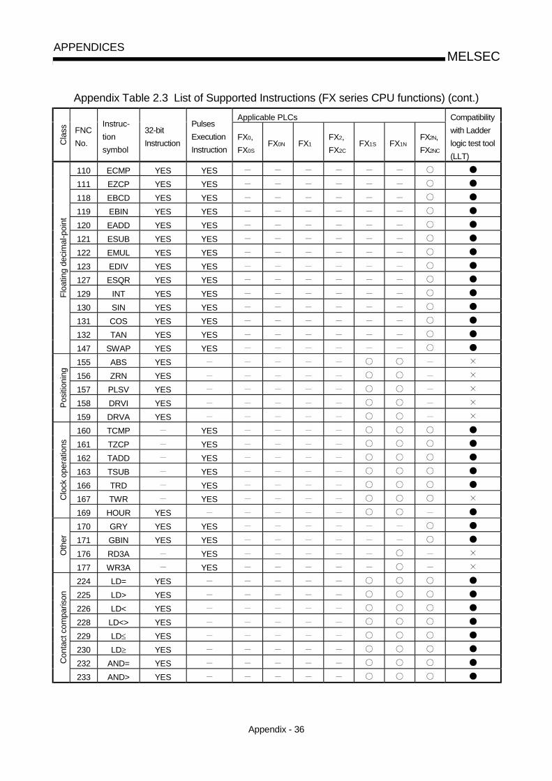
Appendix - 36
MELSECAPPENDICES
Appendix Table 2.3 List of Supported Instructions (FX series CPU functions) (cont.)
Applicable PLCs
Cla
ss FNC
No.
Instruc-
tion
symbol
32-bit
Instruction
Pulses
Execution
Instruction
FX0,
FX0SFX0N FX1
FX2,
FX2CFX1S FX1N
FX2N,
FX2NC
Compatibility
with Ladder
logic test tool
(LLT)
110 ECMP YES YES
111 EZCP YES YES
118 EBCD YES YES
119 EBIN YES YES
120 EADD YES YES
121 ESUB YES YES
122 EMUL YES YES
123 EDIV YES YES
127 ESQR YES YES
129 INT YES YES
130 SIN YES YES
131 COS YES YES
132 TAN YES YES
Flo
atin
g de
cim
al-p
oint
147 SWAP YES YES
155 ABS YES
156 ZRN YES
157 PLSV YES
158 DRVI YESPos
ition
ing
159 DRVA YES
160 TCMP YES
161 TZCP YES
162 TADD YES
163 TSUB YES
166 TRD YES
167 TWR YESClo
ck o
pera
tions
169 HOUR YES
170 GRY YES YES
171 GBIN YES YES
176 RD3A YESOth
er
177 WR3A YES
224 LD= YES
225 LD> YES
226 LD< YES
228 LD<> YES
229 LD≤ YES
230 LD≥ YES
232 AND= YESCon
tact
com
paris
on
233 AND> YES

Appendix - 37
MELSECAPPENDICES
Appendix Table 2.3 List of Supported Instructions (FX series CPU functions) (cont.)
Applicable PLCs
Cla
ss FNC
No.
Instruc-
tion
symbol
32-bit
Instruction
Pulses
Execution
Instruction
FX0,
FX0SFX0N FX1
FX2,
FX2CFX1S FX1N
FX2N,
FX2NC
Compatibility
with Ladder
logic test tool
(LLT)
234 AND< YES
236 AND<> YES
237 AND≤ YES
238 AND≥ YES
240 OR= YES
241 OR> YES
242 OR< YES
244 OR<> YES
245 OR≤ YES
Con
tact
com
paris
on
246 OR≥ YES
: Supported by ladder logic test tool (LLT).
: Not supported by ladder logic test tool (LLT).
: Instruction supported by the actual PLC.
: FX0, FX0S, and FX0N actual PLCs do not support pulse-executed instructions.
: Instruction not supported by the actual PLC.

Appendix - 38
MELSECAPPENDICES
Appendix 2.4 Ladder logic test tool (LLT) for Q series CPU (A mode) functions
Since the supported instructions of the Q series CPU (A mode) are the same as those
of the A series CPU, refer to Appendix Table 2.1 "List of Supported Instructions (A
series CPU Function)".
Appendix 2.5 Ladder logic test tool (LLT) for Q series CPU (Q mode) functions
Appendix Table 2.4 List of Supported Instructions (Q Series CPU (Q Mode) Function)
(1) Sequence Instructions
Class Instruction Symbol Restriction
Contact instructionsLD, LDI, AND, ANI, OP, ORI, LDP, LDF, ANDP,
ANDF, ORP, ORF
Coupling instructionsANB, ORB, MPS, MRD, MPP, INV, MEP, MEF, EGP,
EGF
Output instructionsOUT, OUT T, OUT C, OUTH T, SET, RST, PLS, PLF,
FF
Shift instruction SFT(P)
Master control instructions MC, MCR
End instructions FEND, END
Other instructions STOP, NOP, NOPLF, PAGE
(2) Basic Instructions
Class Instruction Symbol Restriction
Comparative operation
instructions
=, <>, >, <=, <, >=, D=, D<>, D>, D<=, D<, D>=, E=,
E<>, E>, E<=, E<, E>=, $=, $<>, $>, $<=, $<, $>=,
BKCMP (P)
Arithmetic operation
instructions
+(P), -(P), D+(P), D-(P), (P), /(P), D (P), D/(P),
B+(P), B-(P), DB+(P), DB-(P), B (P), B/(P), DB (P),
DB/(P), E+(P), E-(P), E (P), E/(P), BK+(P), BK-(P),
$+(P), INC(P), DEC(P), DINC(P), DDEC(P)
Data conversion instructions
BCD(P), DBCD(P), BIN(P), DBIN(P) INT(P), DINT(P),
FLT(P), DFLT(P), DBL(P), WORD(P), GRY(P),
DGRY(P), GBIN(P), DGBIN(P), NEG(P), DNEG(P),
ENEG(P), BKBCD(P), BKBIN(P)
Data transfer instructions
MOV(P), DMOV(P), EMOV(P), $MOV(P), CML(P),
DCML(P), BMOV(P), FMOV(P), XCH(P), DXCH(P),
BXCH(P), SWAP(P), RBMOV
RBMOV operates as BMOVinstruction.
Program branch instructions CJ, SCJ, JMP, GOEND
Other convenient instructions TTMR, STMR, RAMP, MTR

Appendix - 39
MELSECAPPENDICES
Appendix Table 2.4 List of Supported Instructions (Q Series CPU (Q Mode)Function) (cont.)
(1) Applied Instructions
Class Instruction Symbol Restriction
Logical arithmetic instructions
WAND(P), DAND(P), BKAND(P), WOR(P), DOR(P),
BKOR(P), WXOR(P), DXOR(P), BKXOR(P),
WXNR(P), DXNR(P), BKNXR(P)
Rotation instructionsROR(P), RCR(P), ROL(P), RCL(P), DROR(P),
DRCR(P), DROL(P), DRCL(P)
Shift instructionsSFR(P), SFL(P), BSFR(P), BSFL(P), DSFR(P),
DSFL(P)
Bit processing instructions BSET(P), BRST(P), TEST(P), DTEST(P), BKRST(P),
Data processing instructions
SER(P), DSER(P), SUM(P), DSUM(P), DECO(P),
ENCO(P), SEG(P), DIS(P), UNI(P), NDIS(P),
NUNI(P), WTOB(P), BTOW(P), MAX(P), MIN(P),
DMAX(P), DMIN(P), SORT(P), DSORT(P),
WSUM(P), DWSUM(P)
SORT(P) and DSORT(P) areexecuted in 1 scan.
Structured instructionsFOR, NEXT, BREAK(P), CALL(P), RET, FCALL(P),
ECALL(P), EFCALL(P)
Data table operation
instructionsFIFW(P), FIFR(P), FPOP(P), FINS(P), FDEL(P)
Buffer memory access
instructionsFROM(P), DFRO(P), TO(P), DTO(P)
Character string processing
instructions
BINDA(P), DBINDA(P), BINHA(P), DBINHA(P),
BCDDA(P), DBCDDA(P), DABIN(P), DDABIN(P),
HABIN(P), DHABIN(P), DABCD(P), DDABCD(P),
LEN(P), STR(P), DSTR(P), VAL(P), DVAL(P),
ESTR(P), EVAL(P), ASC(P), HEX(P), RIGHT(P),
LEFT(P), MIDR(P), MIDW(P), INSTR(P), EMOD(P),
EREXP(P)
Special function instructions
SIN(P), COS(P), TAN(P), ASIN(P), ACOS(P),
ATAN(P), RAD(P), DEG(P), SQR(P), EXP(P),
LOG(P), BSQR(P), BDSQR(P), BSIN(P), BCOS(P),
BTAN(P), BASIN(P), BACOS(P), BATAN(P)
Data control instructionsLIMIT(P), DLIMIT(P), BAND(P), DBAND(P),
ZONE(P), DZONE(P), RSET(P), QDRSET(P)
Clock instructionsDATERD(P), DATA+(P), DATA−(P), SECOND(P),
HOUR(P)
DATERD(P) reads clock dataof personal computer.
Program control instructions PSTOP(P), POFF(P), PSCAN(P), PLOW(P)
Display instructions LED, LEDR
Other instructions DUTY, ZRRDB(P), ZRWRB(P), ADRSET(P)

Appendix - 40
MELSECAPPENDICES
Appendix 3 List of Devices Usable with the I/O System Settings
Some devices designated in the condition setting area and simulation device area bythe I/O system settings are subject to restrictions.A list of the devices which can be used with the I/O system settings is shown below.
Simulation device area
<Timing chart input>
<Device value input>
Condition area
Appendix 3.1 Condition area
Devices which can be designated in condition area are the same for both timing chart
input and device value input.
Function
Device NameACPU QnACPU
QCPU
(A mode)
QCPU
(Q mode)FXCPU
Input (X)
Output (Y)
Internal relay (M)
Latch relay (L)
Step relay (S)
Step relay (S) (for SFC)
State (S)
Annunciator (F)
Edge relay (V)
Link special relay (SB)
Link relay (B)
(M)Special relay
(SM)
Contacts 1 1 1 1 1
Bit
devi
ce
Timer (T)Coil
…………...Can be used…………...Cannot be used…………...Not supported
1 : Only T, ST, and C contacts can be designated.2 : In the FX series, the device name becomes
"T".
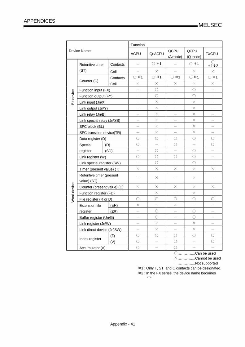
Appendix - 41
MELSECAPPENDICES
Function
Device NameACPU QnACPU
QCPU
(A mode)
QCPU
(Q mode)FXCPU
Contacts 1 11 2Retentive timer
(ST) Coil
Contacts 1 1 1 1 1Counter (C)
Coil
Function input (FX)
Function output (FY)
Link input (Jn\X)
Link output (Jn\Y)
Link relay (Jn\B)
Link special relay (Jn\SB)
SFC block (BL)
Bit
devi
ce
SFC transition device(TR)
Data register (D)
(D)Special
register (SD)
Link register (W)
Link special register (SW)
Timer (present value) (T)
Retentive timer (present
value) (ST)
Counter (present value) (C)
Function register (FD)
File register (R or D)
(ER)Extension file
register (ZR)
Buffer register (Un\G)
Link register (Jn\W)
Link direct device (Jn\SW)
(Z)Index register
(V)
Wor
d de
vice
Accumulator (A)
…………...Can be used…………...Cannot be used…………...Not supported
1 : Only T, ST, and C contacts can be designated.2 : In the FX series, the device name becomes
"T".

Appendix - 42
MELSECAPPENDICES
Appendix 3.2 Simulation device area
(1) Timing chart input
Function
Device NameACPU QnACPU
QCPU
(A mode)
QCPU
(Q mode)FXCPU
Input (X)
Output (Y)
Internal relay (M)
Latch relay (L)
Step relay (S)
Step relay (S) (for SFC)
State (S)
Annunciator (F)
Edge relay (V)
Link special relay (SB)
Link relay (B)
(M)Special relay
(SM)
ContactsTimer (T)
Coil
ContactsRetentive timer
(ST) Coil
ContactsCounter (C)
Coil
Function input (FX)
Function output (FY)
Link input (Jn\X)
Link output (Jn\Y)
Link relay (Jn\B)
Link special relay (Jn\SB)
SFC block (BL)
Bit
devi
ce
SFC transition device(TR)
…………...Can be used
…………...Cannot be used
…………...Not supported

Appendix - 43
MELSECAPPENDICES
Function
Device NameACPU QnACPU
QCPU
(A mode)
QCPU
(Q mode)FXCPU
Data register (D)
(D)Special
register (SD)
Link register (W)
Link special register (SW)
Timer (present value) (T)
Retentive timer (present
value) (ST)
Counter (present value) (C)
Function register (FD)
File register (R or D)
(ER)Extension file
register (ZR)
Buffer register (Un\G)
Link register (Jn\W)
Link direct device (Jn\SW)
(Z)Index register
(V)
Wor
d de
vice
Accumulator (A)
…………...Can be used
…………...Cannot be used
…………...Not supported

Appendix - 44
MELSECAPPENDICES
(2) Device value input
Function
Device NameACPU QnACPU
QCPU
(A mode)
QCPU
(Q mode)FXCPU
Input (X)
Output (Y)
Internal relay (M)
Latch relay (L)
Step relay (S)
Step relay (S) (for SFC)
State (S)
Annunciator (F)
Edge relay (V)
Link special relay (SB)
Link relay (B)
(M)Special relay
(SM)
ContactsTimer (T)
Coil
ContactsRetentive timer
(ST) Coil
ContactsCounter (C)
Coil
Function input (FX)
Function output (FY)
Link input (Jn\X)
Link output (Jn\Y)
Link relay (Jn\B)
Link special relay (Jn\SB)
SFC block (BL)
Bit
devi
ce
SFC transition device(TR)
…………...Can be used
…………...Cannot be used
…………...Not supported

Appendix - 45
MELSECAPPENDICES
Function
Device NameACPU QnACPU
QCPU
(A mode)
QCPU
(Q mode)FXCPU
Data register (D)
(D)Special
register (SD)
Link register (W)
Link special register (SW)
Timer (present value) (T)
Retentive timer (present
value) (ST)
Counter (present value) (C)
Function register (FD)
File register (R or D)
(ER)Extension file
register (ZR)
Buffer register (Un\G)
Link register (Jn\W)
Link direct device (Jn\SW)
(Z)Index register
(V)
Wor
d de
vice
Accumulator (A)
…………...Can be used
…………...Cannot be used
…………...Not supported

Appendix - 46
MELSECAPPENDICES
MEMO

Index - 1
INDEX
[A]
A series CPU
Device list.......................................Appendix- 1
List of instruction...........................Appendix-29
Restrictions and precautions..................... 2-12
[C]
Cautions.......................................................... 2- 9
A series CPU ............................................. 2-12
Common ..................................................... 2- 9
FX series CPU........................................... 2-17
Handling..................................................... 2-24
Motion controller CPU ............................... 2-19
Q series CPU............................................. 2-20
QnA series CPU ........................................ 2-14
Changing the monitor communications......... 5- 7
interval
Condition area ..................................Appendix-40
Conditions....................................................... 4- 2
Configuration of screen
I/O system settings..................................... 4- 6
Timing chart format input screen .............. 4-11
Timing chart screen................................... 5-14
Copy............................................................... 4-31
COS curve ..................................................... 4-18
Creating a new file......................................... 4-29
Cutting............................................................ 4-31
Cutting, copying , pasting set No.................. 4-31
[D]
Device display position exchange .......4-24, 5-25
Device entering/deleting.......................4-13, 5-17
Device list .............................................4-23, 5-24
A series CPU .................................Appendix- 1
Condition area ..............................Appendix-40
FX series CPU..............................Appendix-10
Q series CPU................................Appendix-24
QnA series CPU ............................Appendix- 4
Simulation device area.................Appendix-42
Usable in I/O system settings.......Appendix-40
Device memory monitor
Operation procedure .................................. 5- 2
Outline......................................................... 5- 1
Device memory/buffer memory
Reading .......................................................6- 3
Saving..........................................................6- 1
Device selection..............................................5- 4
Device test......................................................5-10
Device value input..........................................4-25
Devices and instructions.................................2- 8
Differences ......................................................1- 5
Display format ..............................4-23, 5- 8, 5-24
[E]
Ending
Device memory monitor..............................5- 3
I/O system settings......................................4- 5
Ladder logic test tool (LLT) .........................3- 6
Timing chart................................................5-13
Error message ................................................8- 1
Exchange ............................................. 4-24, 5-25
[F]
Features ..........................................................1- 2
Function list .....................................................2- 3
FX series CPU
Device list ..................................... Appendix-10
List of supported instruction......... Appendix-33
Restrictions and precautions .....................2-17
[G]
GPPW operations ...........................................3- 3
[H]
Handling precautions .....................................2-24
[I]
I/O system settings
Configuration of screen...............................4- 6
List of usable devices................... Appendix-40
Operation procedure ...................................4- 4
Outline .........................................................4- 1
Initial window...................................................3- 5
Instruction list
A series CPU................................ Appendix-29
FX series CPU.............................. Appendix-33
Q series CPU ............................... Appendix-38
QnA series CPU........................... Appendix-31

Index - 2
[M]
Monitor communications interval ................... 5- 7
Monitor execution.......................................... 4-32
Monitor format ................................................ 5- 8
Monitor starting/stopping............................... 5-20
Monitor stopping/restarting ............................ 5- 6
Motion controller CPU
Restrictions and precautions..................... 2-19
[O]
Opening
I/O system setting file ................................ 4-29
New window................................................ 5- 9
Timing data file .......................................... 5-21
Opening the new window............................... 5- 9
Operation procedure
Common ..................................................... 3- 1
Device memory monitor ............................. 5- 2
I/O system settings..................................... 4- 4
Timing chart ............................................... 5-12
Timing chart format input screen .............. 4-10
Outline............................................................. 1- 1
[P]
Pasting........................................................... 4-31
[Q]
Q series CPU
Device list......................................Appendix-24
List of supported instruction .........Appendix-38
Restrictions and precautions..................... 2-20
QnA series CPU
Device list.......................................Appendix- 4
List of supported instruction .........Appendix-31
Restrictions and precautions..................... 2-14
[R]
Reading ......................................................... 4-34
Reading file.................................................... 4-22
Restrictions..................................................... 2- 9
A series CPU ............................................. 2-12
Common ..................................................... 2- 9
FX series CPU........................................... 2-17
Motion controller CPU ............................... 2-19
Q series CPU............................................. 2-20
QnA series CPU ........................................ 2-14
[S]
Sampling period .............................................5-23
Saving ............................................................4-30
Saving in file...................................................5-21
Saving with new name...................................4-30
Scan number........................................ 4-12, 4-21
Simulation device area .................... Appendix-42
Simulation example ........................................7- 1
SIN curve........................................................4-18
Specifications..................................................2- 1
Starting
Device memory monitor..............................5- 3
I/O system settings......................................4- 5
Timing chart................................................5-13
Starting/stopping .................................. 4-27, 5-20
Starting/stopping the simulation ....................4-27
Stopping and restarting...................................5- 6
Supported devices and instructions ...............2- 8
[T]
Test.................................................................5-10
Timing chart
Operation procedure ..................................5-12
Screen configuration ..................................5-14
Usable devices...........................................5-27
Timing chart format input screen
Operation procedure ..................................4-10
Screen configuration ..................................4-11
Timing chart input ...........................................4- 8
Timing data saving.........................................5-21
Timing setting/editing
Bit device ....................................................4-15
Word device ...............................................4-17
Troubleshooting ..............................................8- 1
[U]
Undoing..........................................................4-22

When exported from Japan, this manual does not require application to theMinistry of International Trade and Industry for service transaction permission.
Specifications subject to change without notice.
HEAD OFFICE : MITSUBISHI DENKI BLDG MARUNOUCHI TOKYO 100-8310 TELEX : J24532 CABLE MELCO TOKYONAGOYA WORKS : 1-14 , YADA-MINAMI 5 , HIGASHI-KU, NAGOYA , JAPAN
MODEL
MODELCODE
SW5D5C-LLT-O-E
13J977
SH(NA)-080064-C(0011)MEE