large-scale all-dielectric metamaterial perfect reflectors · large-scale all-dielectric...
TRANSCRIPT
Large-Scale All-Dielectric Metamaterial Perfect ReflectorsParikshit Moitra,† Brian A. Slovick,‡ Wei li,§ Ivan I. Kravchencko,∥ Dayrl P. Briggs,∥ S. Krishnamurthy,‡
and Jason Valentine*,§
†Interdisciplinary Materials Science Program and §Department of Mechanical Engineering, Vanderbilt University, Nashville,Tennessee 37212, United States‡Applied Optics Laboratory, SRI International, Menlo Park, California 94025, United States∥Center for Nanophase Materials Sciences, Oak Ridge National Laboratory, Oak Ridge, Tennessee 37831, United States
ABSTRACT: All-dielectric metamaterials offer a potential low-lossalternative to plasmonic metamaterials at optical frequencies. Here,we take advantage of the low absorption loss as well as the simple unitcell geometry to demonstrate large-scale (centimeter-sized) all-dielectricmetamaterial perfect reflectors made from silicon cylinder resonators.These perfect reflectors, operating in the telecommunications band,were fabricated using self-assembly based nanosphere lithography.In spite of the disorder originating from the self-assembly process, theaverage reflectance of the metamaterial perfect reflectors is 99.7% at 1530 nm, surpassing the reflectance of metallic mirrors.Moreover, the spectral separation of the electric and magnetic resonances can be chosen to achieve the required reflectionbandwidth while maintaining a high tolerance to disorder. The scalability of this design could lead to new avenues ofmanipulating light for low-loss and large-area photonic applications.
KEYWORDS: all-dielectric metamaterial, perfect reflector, nanosphere lithography, Mie resonance
Recently, there has been great interest in finding alternativesto metal-based metamaterials (MMs) in an effort to
overcome the free-carrier absorption found in metals at opticalfrequencies.1−3 Additionally, metallic unit cells often exhibitcomplicated geometries that render the optical responseanisotropic3 and necessitate the use of nanoscale lithographytechniques, such as electron beam lithography, to pattern theunit cells. These patterning techniques are slow and expensive,prohibiting the designs from being scaled to large areas.Dielectric metamaterials4−10 based on electric and magneticMie resonances4,6,11−16 in transparent dielectric particles providea lower-loss alternative to metal-based MMs. Furthermore, dueto their simple unit cell geometries such as spheres, cubes,cylinders, and rods,4,5,16−18 dielectric MMs can potentially bepatterned with alternative techniques that allow scaling to largeareas.In recent work, we have demonstrated near-perfect broad-
band reflection in the telecommunications band using single-negative metamaterials formed from both periodic anddisordered lattices of silicon (Si) cylinders.15,19 Although gold(Au) and silver (Ag) mirrors exhibit high reflection they stillabsorb ∼2% of light in this band. In place of metallic mirrors,distributed Bragg reflectors (DBRs), made of alternatingdielectric layers, are typically used for achieving near-perfectreflection. The primary disadvantage of Bragg reflectors isthat the deposition of multiple dielectric materials is a lengthyprocess which adds to the cost of the product. Realization ofperfect reflection from a single-layer large-scale metamaterial,which forms the basis of this article, offers advantages in termsof simple, high-throughput, and low-cost fabrication, and in
turn opens the door to future paint-like coatings of meta-materials for even larger-area implementation.Additionally, the metamaterial approach provides the free-
dom to manipulate both the magnetic and electric response ofthe reflector. Conventional mirrors made from metal and Braggreflectors operate as electric mirrors in which the reflected electricfield undergoes a 180° phase change resulting in an electric fieldminimum at the mirror surface. Dielectric metamaterial perfectreflectors can exhibit perfect reflection due to both electric andmagnetic dipole Mie resonances.8,15,19,20 In this case, the phaseof the reflected electric field can be swept from 180° to 0° bymoving from the electric to the magnetic resonance.20,21 Mostimportantly, at the magnetic resonance a reflection phase shiftof 0° results in an electric field maximum at the surface of thematerial, strongly enhancing the light−matter interaction22 ofmaterials placed on the mirror. This field enhancement could beuseful for applications, such as surface-enhanced Raman spec-troscopy or SERS.In our previous work,15 electron beam lithography was used
for a proof-of-concept demonstration of a dielectric meta-material reflector with a sample size of 100 μm × 100 μm.However, for large-area applications, electron beam lithographyis impractical. Here, we describe the design and fabrication oflarge-scale (centimeter-sized) MM perfect reflectors based onsilicon (Si) cylinder resonators. Silicon is used as the resonatorelement due to its transparency and large permittivity at infraredfrequencies, as well as its well-developed top-down nanofabrication
Received: March 25, 2015Published: May 8, 2015
Letter
pubs.acs.org/journal/apchd5
© 2015 American Chemical Society 692 DOI: 10.1021/acsphotonics.5b00148ACS Photonics 2015, 2, 692−698
Dow
nloa
ded
by V
AN
DE
RB
ILT
UN
IV o
n Se
ptem
ber
11, 2
015
| http
://pu
bs.a
cs.o
rg
Pub
licat
ion
Dat
e (W
eb):
May
14,
201
5 | d
oi: 1
0.10
21/a
csph
oton
ics.
5b00
148
processes. Cylindrical resonators are used because they allowspectral separation of the electric and magnetic Mie resonancesby changing the aspect ratio (AR) and can be patterned bynanosphere lithography and reactive ion etching (RIE). Usingthis platform, we demonstrate near-perfect reflection over largecentimeter-sized areas with around half a billion resonatorscomprising the metamaterial. In addition, by studying theeffect of lattice disorder originating from the self-assemblypatterning process, it was found that the reflectance due to themagnetic resonance is more tolerant to disorder than theelectric resonance due to better confinement of the opticalmode. This research could lead to the use of large-scale perfectreflectors within the telecommunication band for large-areaapplications.The conditions needed to achieve perfect reflection using
a thin slab of material are described in the literature.19 The firstcondition is complete impedance mismatch with air, namely,the real part of the impedance must be zero. This conditionis achieved when ε′/μ′ < 0 (single-negative MM) and ε″μ′ =ε′μ″, where the complex permittivity and permeability aregiven by ε′ + iε″ and μ′ + iμ″, respectively. The single-negativecondition can be satisfied at electric or magnetic resonances,provided that the resonances are spectrally separated. Theequation ε″μ′ = ε′μ″ is more restrictive but is convenientlysatisfied by lossless materials. The second condition for perfectreflection is that the imaginary part of the index (n″) needs tobe large to prohibit any evanescent tunneling of light throughthe slab.One way to achieve the conditions for perfect reflection is
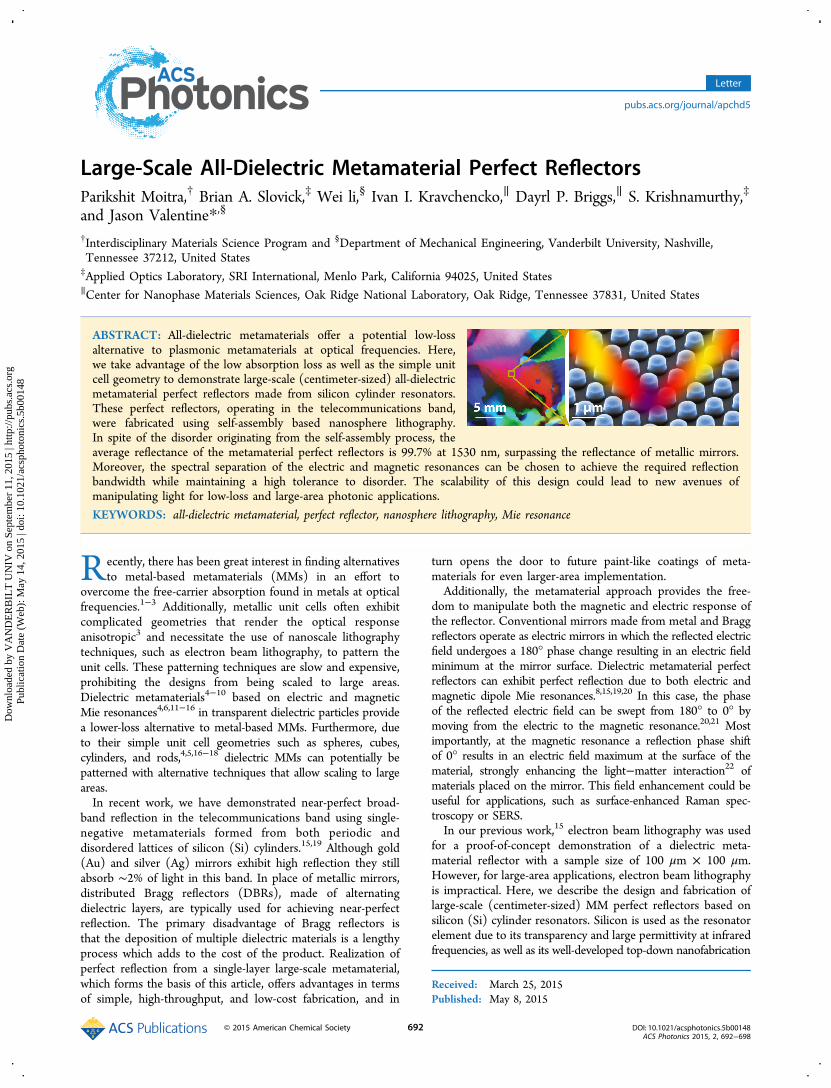
to use electric and magnetic dipole resonances of Si cylinderresonators. In particular, here we arrange the resonators in ahexagonal lattice (Figure 1a) to realize a single-negative meta-material. S-parameter retrieval23−25 was performed to extracteffective metamaterial properties using the complex transmissionand reflection coefficients, which were numerically calculatedusing full-wave simulations (CST Microwave Studio). Figure 1billustrates the properties of the metamaterial, namely a regionwhere ε′ < 0 and μ′ > 0(electric dipole resonance) at anormalized wavelength (λn = λ/P, where P is the lattice period)of 1.34 and μ′ < 0 and ε′ > 0 (magnetic dipole resonance) ata normalized wavelength of 1.65. Figure 1c shows themetamaterial reflection spectra, demonstrating perfect reflectionat these two wavelengths. The inset shows the correspondingelectric and magnetic field plots, illustrating that the tworeflection peaks correspond to electric and magnetic dipoleresonances.In order to fabricate the metamaterial on a large scale,
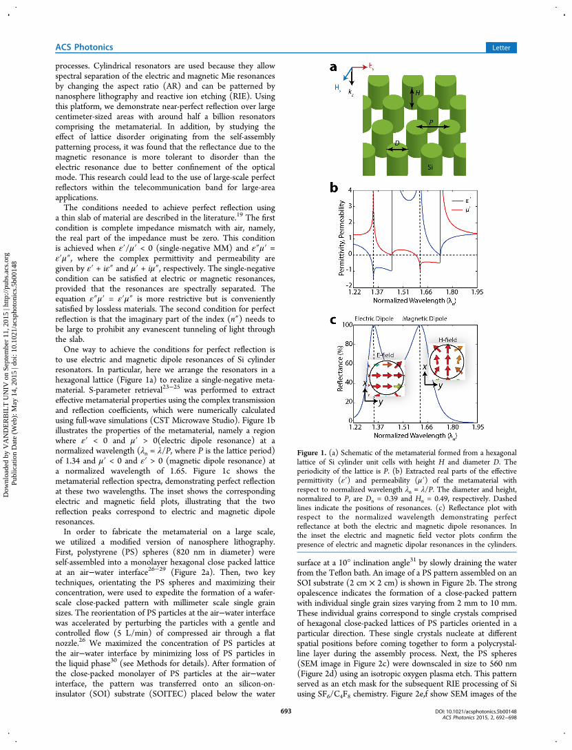
we utilized a modified version of nanosphere lithography.First, polystyrene (PS) spheres (820 nm in diameter) wereself-assembled into a monolayer hexagonal close packed latticeat an air−water interface26−29 (Figure 2a). Then, two keytechniques, orientating the PS spheres and maximizing theirconcentration, were used to expedite the formation of a wafer-scale close-packed pattern with millimeter scale single grainsizes. The reorientation of PS particles at the air−water interfacewas accelerated by perturbing the particles with a gentle andcontrolled flow (5 L/min) of compressed air through a flatnozzle.26 We maximized the concentration of PS particles atthe air−water interface by minimizing loss of PS particles inthe liquid phase30 (see Methods for details). After formation ofthe close-packed monolayer of PS particles at the air−waterinterface, the pattern was transferred onto an silicon-on-insulator (SOI) substrate (SOITEC) placed below the water
surface at a 10° inclination angle31 by slowly draining the waterfrom the Teflon bath. An image of a PS pattern assembled on anSOI substrate (2 cm × 2 cm) is shown in Figure 2b. The strongopalescence indicates the formation of a close-packed patternwith individual single grain sizes varying from 2 mm to 10 mm.These individual grains correspond to single crystals comprisedof hexagonal close-packed lattices of PS particles oriented in aparticular direction. These single crystals nucleate at differentspatial positions before coming together to form a polycrystal-line layer during the assembly process. Next, the PS spheres(SEM image in Figure 2c) were downscaled in size to 560 nm(Figure 2d) using an isotropic oxygen plasma etch. This patternserved as an etch mask for the subsequent RIE processing of Siusing SF6/C4F8 chemistry. Figure 2e,f show SEM images of the
Figure 1. (a) Schematic of the metamaterial formed from a hexagonallattice of Si cylinder unit cells with height H and diameter D. Theperiodicity of the lattice is P. (b) Extracted real parts of the effectivepermittivity (ε′) and permeability (μ′) of the metamaterial withrespect to normalized wavelength λn = λ/P. The diameter and height,normalized to P, are Dn = 0.39 and Hn = 0.49, respectively. Dashedlines indicate the positions of resonances. (c) Reflectance plot withrespect to the normalized wavelength demonstrating perfectreflectance at both the electric and magnetic dipole resonances. Inthe inset the electric and magnetic field vector plots confirm thepresence of electric and magnetic dipolar resonances in the cylinders.
ACS Photonics Letter
DOI: 10.1021/acsphotonics.5b00148ACS Photonics 2015, 2, 692−698
693
Dow
nloa
ded
by V
AN
DE
RB
ILT
UN
IV o
n Se
ptem
ber
11, 2
015
| http
://pu
bs.a
cs.o
rg
Pub
licat
ion
Dat
e (W
eb):
May
14,
201
5 | d
oi: 1
0.10
21/a
csph
oton
ics.
5b00
148
top and isometric views of the final metamaterial (after removalof PS mask) consisting of Si cylinders (Dtop = 480 nm, Dbottom =554 nm, H = 335 nm, and P = 820 nm) arranged in a hexagonallattice. The SEM images along with the optical image clearlydemonstrate that nanosphere lithography can yield high qualitydielectric resonators over a large area.The size variations in PS spheres (coefficient of variance
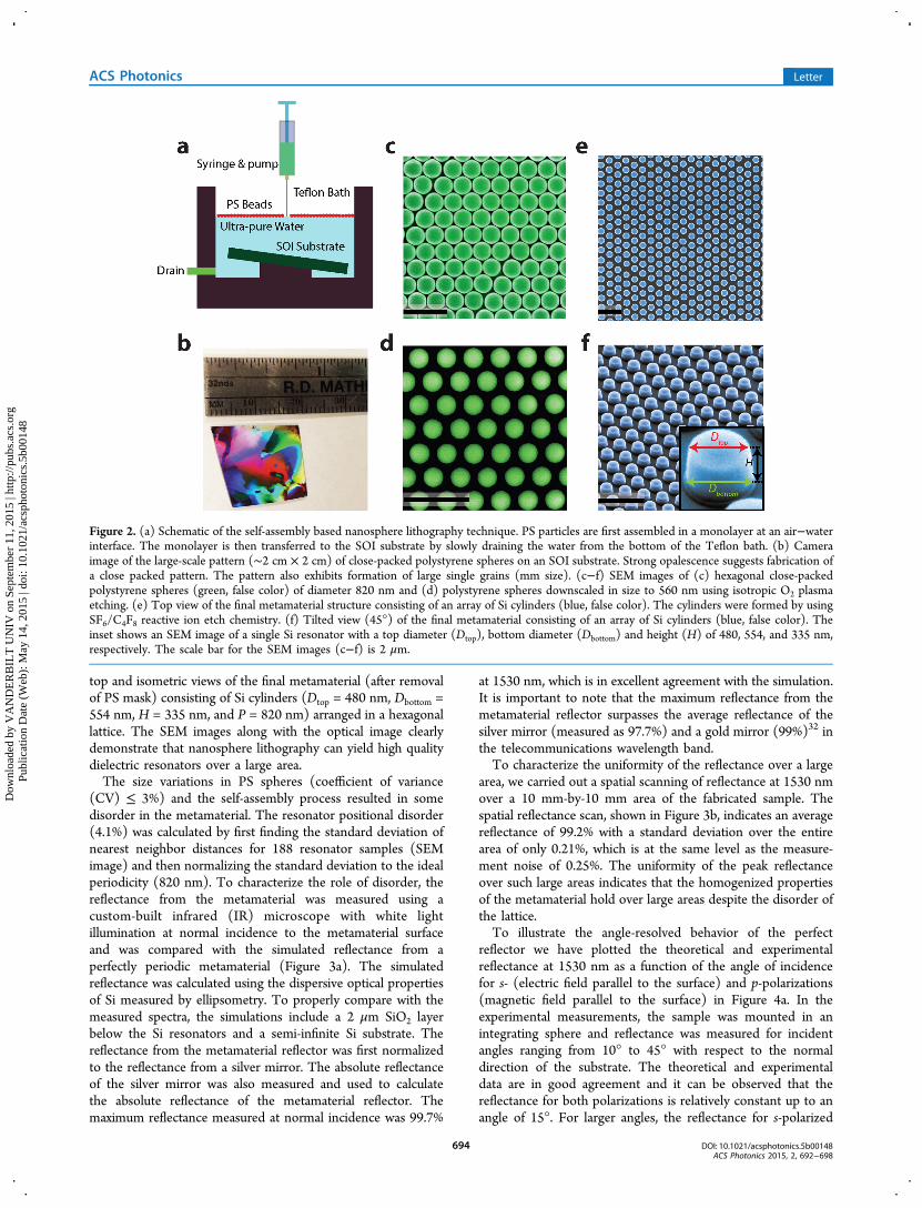
(CV) ≤ 3%) and the self-assembly process resulted in somedisorder in the metamaterial. The resonator positional disorder(4.1%) was calculated by first finding the standard deviation ofnearest neighbor distances for 188 resonator samples (SEMimage) and then normalizing the standard deviation to the idealperiodicity (820 nm). To characterize the role of disorder, thereflectance from the metamaterial was measured using acustom-built infrared (IR) microscope with white lightillumination at normal incidence to the metamaterial surfaceand was compared with the simulated reflectance from aperfectly periodic metamaterial (Figure 3a). The simulatedreflectance was calculated using the dispersive optical propertiesof Si measured by ellipsometry. To properly compare with themeasured spectra, the simulations include a 2 μm SiO2 layerbelow the Si resonators and a semi-infinite Si substrate. Thereflectance from the metamaterial reflector was first normalizedto the reflectance from a silver mirror. The absolute reflectanceof the silver mirror was also measured and used to calculatethe absolute reflectance of the metamaterial reflector. Themaximum reflectance measured at normal incidence was 99.7%
at 1530 nm, which is in excellent agreement with the simulation.It is important to note that the maximum reflectance from themetamaterial reflector surpasses the average reflectance of thesilver mirror (measured as 97.7%) and a gold mirror (99%)32 inthe telecommunications wavelength band.To characterize the uniformity of the reflectance over a large
area, we carried out a spatial scanning of reflectance at 1530 nmover a 10 mm-by-10 mm area of the fabricated sample. Thespatial reflectance scan, shown in Figure 3b, indicates an averagereflectance of 99.2% with a standard deviation over the entirearea of only 0.21%, which is at the same level as the measure-ment noise of 0.25%. The uniformity of the peak reflectanceover such large areas indicates that the homogenized propertiesof the metamaterial hold over large areas despite the disorder ofthe lattice.To illustrate the angle-resolved behavior of the perfect
reflector we have plotted the theoretical and experimentalreflectance at 1530 nm as a function of the angle of incidencefor s- (electric field parallel to the surface) and p-polarizations(magnetic field parallel to the surface) in Figure 4a. In theexperimental measurements, the sample was mounted in anintegrating sphere and reflectance was measured for incidentangles ranging from 10° to 45° with respect to the normaldirection of the substrate. The theoretical and experimentaldata are in good agreement and it can be observed that thereflectance for both polarizations is relatively constant up to anangle of 15°. For larger angles, the reflectance for s-polarized
Figure 2. (a) Schematic of the self-assembly based nanosphere lithography technique. PS particles are first assembled in a monolayer at an air−waterinterface. The monolayer is then transferred to the SOI substrate by slowly draining the water from the bottom of the Teflon bath. (b) Cameraimage of the large-scale pattern (∼2 cm × 2 cm) of close-packed polystyrene spheres on an SOI substrate. Strong opalescence suggests fabrication ofa close packed pattern. The pattern also exhibits formation of large single grains (mm size). (c−f) SEM images of (c) hexagonal close-packedpolystyrene spheres (green, false color) of diameter 820 nm and (d) polystyrene spheres downscaled in size to 560 nm using isotropic O2 plasmaetching. (e) Top view of the final metamaterial structure consisting of an array of Si cylinders (blue, false color). The cylinders were formed by usingSF6/C4F8 reactive ion etch chemistry. (f) Tilted view (45°) of the final metamaterial consisting of an array of Si cylinders (blue, false color). Theinset shows an SEM image of a single Si resonator with a top diameter (Dtop), bottom diameter (Dbottom) and height (H) of 480, 554, and 335 nm,respectively. The scale bar for the SEM images (c−f) is 2 μm.
ACS Photonics Letter
DOI: 10.1021/acsphotonics.5b00148ACS Photonics 2015, 2, 692−698
694
Dow
nloa
ded
by V
AN
DE
RB
ILT
UN
IV o
n Se
ptem
ber
11, 2
015
| http
://pu
bs.a
cs.o
rg
Pub
licat
ion
Dat
e (W
eb):
May
14,
201
5 | d
oi: 1
0.10
21/a
csph
oton
ics.
5b00
148
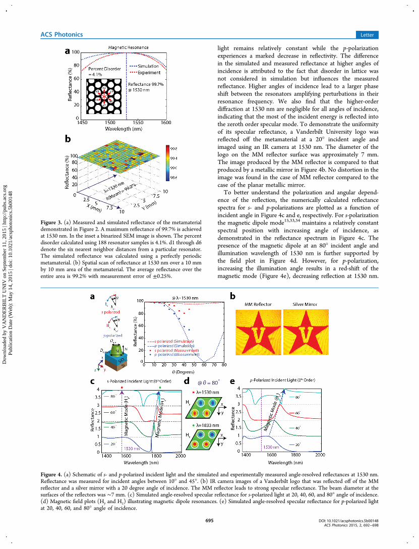
light remains relatively constant while the p-polarizationexperiences a marked decrease in reflectivity. The differencein the simulated and measured reflectance at higher angles ofincidence is attributed to the fact that disorder in lattice wasnot considered in simulation but influences the measuredreflectance. Higher angles of incidence lead to a larger phaseshift between the resonators amplifying perturbations in theirresonance frequency. We also find that the higher-orderdiffraction at 1530 nm are negligible for all angles of incidence,indicating that the most of the incident energy is reflected intothe zeroth order specular mode. To demonstrate the uniformityof its specular reflectance, a Vanderbilt University logo wasreflected off the metamaterial at a 20° incident angle andimaged using an IR camera at 1530 nm. The diameter of thelogo on the MM reflector surface was approximately 7 mm.The image produced by the MM reflector is compared to thatproduced by a metallic mirror in Figure 4b. No distortion in theimage was found in the case of MM reflector compared to thecase of the planar metallic mirror.To better understand the polarization and angular depend-
ence of the reflection, the numerically calculated reflectancespectra for s- and p-polarizations are plotted as a function ofincident angle in Figure 4c and e, respectively. For s-polarizationthe magnetic dipole mode15,33,34 maintains a relatively constantspectral position with increasing angle of incidence, asdemonstrated in the reflectance spectrum in Figure 4c. Thepresence of the magnetic dipole at an 80° incident angle andillumination wavelength of 1530 nm is further supported bythe field plot in Figure 4d. However, for p-polarization,increasing the illumination angle results in a red-shift of themagnetic mode (Figure 4e), decreasing reflection at 1530 nm.
Figure 3. (a) Measured and simulated reflectance of the metamaterialdemonstrated in Figure 2. A maximum reflectance of 99.7% is achievedat 1530 nm. In the inset a binarized SEM image is shown. The percentdisorder calculated using 188 resonator samples is 4.1%. d1 through d6denote the six nearest neighbor distances from a particular resonator.The simulated reflectance was calculated using a perfectly periodicmetamaterial. (b) Spatial scan of reflectance at 1530 nm over a 10 mmby 10 mm area of the metamaterial. The average reflectance over theentire area is 99.2% with measurement error of ±0.25%.
Figure 4. (a) Schematic of s- and p-polarized incident light and the simulated and experimentally measured angle-resolved reflectances at 1530 nm.Reflectance was measured for incident angles between 10° and 45°. (b) IR camera images of a Vanderbilt logo that was reflected off of the MMreflector and a silver mirror with a 20 degree angle of incidence. The MM reflector leads to strong specular reflectance. The beam diameter at thesurfaces of the reflectors was ∼7 mm. (c) Simulated angle-resolved specular reflectance for s-polarized light at 20, 40, 60, and 80° angle of incidence.(d) Magnetic field plots (Hy and Hz) illustrating magnetic dipole resonances. (e) Simulated angle-resolved specular reflectance for p-polarized lightat 20, 40, 60, and 80° angle of incidence.
ACS Photonics Letter
DOI: 10.1021/acsphotonics.5b00148ACS Photonics 2015, 2, 692−698
695
Dow
nloa
ded
by V
AN
DE
RB
ILT
UN
IV o
n Se
ptem
ber
11, 2
015
| http
://pu
bs.a
cs.o
rg
Pub
licat
ion
Dat
e (W
eb):
May
14,
201
5 | d
oi: 1
0.10
21/a
csph
oton
ics.
5b00
148
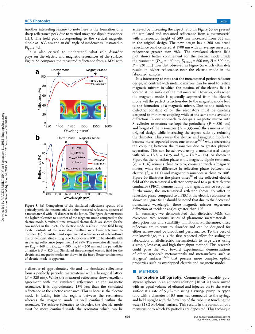
Another interesting feature to note here is the formation of asharp reflectance peak due to vertical magnetic dipole resonance(Hz). The field plot corresponding to the vertical magneticdipole at 1833 nm and an 80° angle of incidence is illustrated inFigure 4d.It is also critical to understand what role disorder
plays on the electric and magnetic resonances of the surface.Figure 5a compares the measured reflectance from a MM with
a disorder of approximately 4% and the simulated reflectancefrom a perfectly periodic metamaterial with a hexagonal lattice(P = 820 nm). While the measured reflectance shows excellentagreement with the simulated reflectance at the magneticresonance, it is approximately 15% less than the simulatedreflectance at the electric resonance. This is because the electricmode is leaking into the regions between the resonators,whereas the magnetic mode is well confined within theresonator. To achieve tolerance to disorder, the electric modemust be more confined inside the resonator which can be
achieved by increasing the aspect ratio. In Figure 5b we presentthe simulated and measured reflectance from a metamaterialwith a resonator height of 500 nm, increased from 335 nmin the original design. The new design has a 200 nm broadreflectance band centered at 1700 nm with an average measuredreflectance greater than 98%. The simulated electric fieldplot shows better confinement for the electric mode insidethe resonators (Dtop = 460 nm, Dbottom = 600 nm, H = 500 nm,P = 820 nm) than that observed in Figure 5a which ultimatelyresults in higher reflectance near the electric mode in thefabricated samples.It is interesting to note that the metamaterial perfect reflector
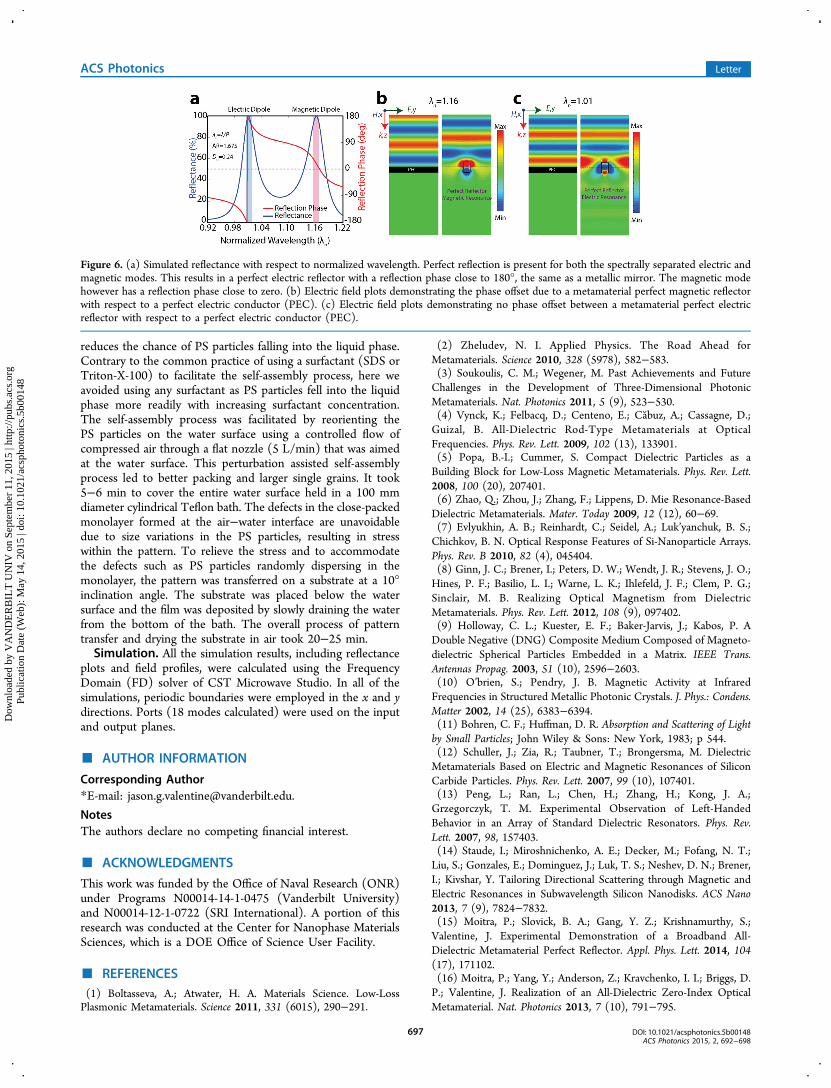
design, in contrast with metallic mirrors, can be used to realizemagnetic mirrors in which the maxima of the electric field islocated at the surface of the metamaterial. However, only whenthe magnetic mode is spectrally separated from the electricmode will the perfect reflection due to the magnetic mode leadto the formation of a magnetic mirror. Due to the moderatedielectric constant of Si, the resonators must be carefullydesigned to minimize coupling while at the same time avoidingdiffraction. In our approach to design a magnetic mirror withSi cylinder resonators we kept the periodicity (P = 820 nm)and height of the resonators (H = 335 nm) the same as in theoriginal design while increasing the aspect ratio by reducingthe diameter. This causes the electric and magnetic modes tobecome more separated from one another14,15 while decreasingthe coupling between the resonators due to greater physicalseparation. This can be achieved using a metamaterial designwith AR = H/D = 1.675 and Dn = D/P = 0.24. As shown inFigure 6a, the reflection phase at the magnetic-dipole resonance(λn = 1.16) remains close to zero, consistent with a magneticmirror, while the difference in reflection phase between theelectric (λn = 1.01) and magnetic resonances is close to 180°.Figure 6b illustrates the phase offset20 of the reflected electricfield of the metamaterial reflector compared to a perfect electricconductor (PEC), demonstrating the magnetic mirror response.Furthermore, the metamaterial reflector shows no offset inreflection phase compared to a PEC at the electric resonance, asshown in Figure 6c. It should be noted that due to the decreasednormalized wavelength, these magnetic mirrors experiencediffraction at incident angles greater than 10°.In summary, we demonstrated that dielectric MMs can
overcome two serious issues of plasmonic metamaterialsabsorption loss and scalability limitations. Furthermore, thesereflectors are tolerant to disorder and can be designed foreither narrowband or broadband performance. To the best ofour knowledge, this is the first reported effort for scaling upfabrication of all-dielectric metamaterials to large areas usinga simple, low-cost, and high-throughput method. This researchcould pave the way toward experimental demonstrationsof other large-scale metamaterials and metasurfaces, such asHuygens’ surfaces,14,35 that possess more complex opticalproperties such as overlapped electric and magnetic modes.
■ METHODSNanosphere Lithography. Commercially available poly-
styrene spheres in an aqueous solution (10 wt %) were mixedwith an equal volume of ethanol and injected on to the watersurface at a rate of 5 μL/min using a syringe pump. A tygontube with a diameter of 0.5 mm was connected to the syringeand held upright with the bevel tip of the tube just touching thewater (18.2 M-Ohm) surface. This results in the formation of ameniscus onto which PS particles are deposited. This technique
Figure 5. (a) Comparison of the simulated reflectance spectra of aperfectly periodic metamaterial and the measured reflectance spectra ofa metamaterial with 4% disorder in the lattice. The figure demonstratesthe higher tolerance to disorder of the magnetic mode compared to theelectric mode. Simulated time-averaged electric fields are shown for thetwo modes in the inset. The electric mode results in more field beinglocated outside of the resonator, resulting in a lower tolerance todisorder. (b) Simulated and experimental reflectances of a broadbandmirror demonstrating strong reflectance over a 200 nm bandwidth withan average reflectance (experiment) of 98%. The resonator dimensionsare Dtop = 460 nm, Dbottom = 600 nm, H = 500 nm and the periodicityof lattice is P = 820 nm. Simulated time-averaged electric field for theelectric and magnetic modes are shown in the inset. Better confinementof electric mode is apparent.
ACS Photonics Letter
DOI: 10.1021/acsphotonics.5b00148ACS Photonics 2015, 2, 692−698
696
Dow
nloa
ded
by V
AN
DE
RB
ILT
UN
IV o
n Se
ptem
ber
11, 2
015
| http
://pu
bs.a
cs.o
rg
Pub
licat
ion
Dat
e (W
eb):
May
14,
201
5 | d
oi: 1
0.10
21/a
csph
oton
ics.
5b00
148
reduces the chance of PS particles falling into the liquid phase.Contrary to the common practice of using a surfactant (SDS orTriton-X-100) to facilitate the self-assembly process, here weavoided using any surfactant as PS particles fell into the liquidphase more readily with increasing surfactant concentration.The self-assembly process was facilitated by reorienting thePS particles on the water surface using a controlled flow ofcompressed air through a flat nozzle (5 L/min) that was aimedat the water surface. This perturbation assisted self-assemblyprocess led to better packing and larger single grains. It took5−6 min to cover the entire water surface held in a 100 mmdiameter cylindrical Teflon bath. The defects in the close-packedmonolayer formed at the air−water interface are unavoidabledue to size variations in the PS particles, resulting in stresswithin the pattern. To relieve the stress and to accommodatethe defects such as PS particles randomly dispersing in themonolayer, the pattern was transferred on a substrate at a 10°inclination angle. The substrate was placed below the watersurface and the film was deposited by slowly draining the waterfrom the bottom of the bath. The overall process of patterntransfer and drying the substrate in air took 20−25 min.Simulation. All the simulation results, including reflectance
plots and field profiles, were calculated using the FrequencyDomain (FD) solver of CST Microwave Studio. In all of thesimulations, periodic boundaries were employed in the x and ydirections. Ports (18 modes calculated) were used on the inputand output planes.
■ AUTHOR INFORMATION
Corresponding Author*E-mail: [email protected].
NotesThe authors declare no competing financial interest.
■ ACKNOWLEDGMENTS
This work was funded by the Office of Naval Research (ONR)under Programs N00014-14-1-0475 (Vanderbilt University)and N00014-12-1-0722 (SRI International). A portion of thisresearch was conducted at the Center for Nanophase MaterialsSciences, which is a DOE Office of Science User Facility.
■ REFERENCES(1) Boltasseva, A.; Atwater, H. A. Materials Science. Low-LossPlasmonic Metamaterials. Science 2011, 331 (6015), 290−291.
(2) Zheludev, N. I. Applied Physics. The Road Ahead forMetamaterials. Science 2010, 328 (5978), 582−583.(3) Soukoulis, C. M.; Wegener, M. Past Achievements and FutureChallenges in the Development of Three-Dimensional PhotonicMetamaterials. Nat. Photonics 2011, 5 (9), 523−530.(4) Vynck, K.; Felbacq, D.; Centeno, E.; Cabuz, A.; Cassagne, D.;Guizal, B. All-Dielectric Rod-Type Metamaterials at OpticalFrequencies. Phys. Rev. Lett. 2009, 102 (13), 133901.(5) Popa, B.-I.; Cummer, S. Compact Dielectric Particles as aBuilding Block for Low-Loss Magnetic Metamaterials. Phys. Rev. Lett.2008, 100 (20), 207401.(6) Zhao, Q.; Zhou, J.; Zhang, F.; Lippens, D. Mie Resonance-BasedDielectric Metamaterials. Mater. Today 2009, 12 (12), 60−69.(7) Evlyukhin, A. B.; Reinhardt, C.; Seidel, A.; Luk’yanchuk, B. S.;Chichkov, B. N. Optical Response Features of Si-Nanoparticle Arrays.Phys. Rev. B 2010, 82 (4), 045404.(8) Ginn, J. C.; Brener, I.; Peters, D. W.; Wendt, J. R.; Stevens, J. O.;Hines, P. F.; Basilio, L. I.; Warne, L. K.; Ihlefeld, J. F.; Clem, P. G.;Sinclair, M. B. Realizing Optical Magnetism from DielectricMetamaterials. Phys. Rev. Lett. 2012, 108 (9), 097402.(9) Holloway, C. L.; Kuester, E. F.; Baker-Jarvis, J.; Kabos, P. ADouble Negative (DNG) Composite Medium Composed of Magneto-dielectric Spherical Particles Embedded in a Matrix. IEEE Trans.Antennas Propag. 2003, 51 (10), 2596−2603.(10) O’brien, S.; Pendry, J. B. Magnetic Activity at InfraredFrequencies in Structured Metallic Photonic Crystals. J. Phys.: Condens.Matter 2002, 14 (25), 6383−6394.(11) Bohren, C. F.; Huffman, D. R. Absorption and Scattering of Lightby Small Particles; John Wiley & Sons: New York, 1983; p 544.(12) Schuller, J.; Zia, R.; Taubner, T.; Brongersma, M. DielectricMetamaterials Based on Electric and Magnetic Resonances of SiliconCarbide Particles. Phys. Rev. Lett. 2007, 99 (10), 107401.(13) Peng, L.; Ran, L.; Chen, H.; Zhang, H.; Kong, J. A.;Grzegorczyk, T. M. Experimental Observation of Left-HandedBehavior in an Array of Standard Dielectric Resonators. Phys. Rev.Lett. 2007, 98, 157403.(14) Staude, I.; Miroshnichenko, A. E.; Decker, M.; Fofang, N. T.;Liu, S.; Gonzales, E.; Dominguez, J.; Luk, T. S.; Neshev, D. N.; Brener,I.; Kivshar, Y. Tailoring Directional Scattering through Magnetic andElectric Resonances in Subwavelength Silicon Nanodisks. ACS Nano2013, 7 (9), 7824−7832.(15) Moitra, P.; Slovick, B. A.; Gang, Y. Z.; Krishnamurthy, S.;Valentine, J. Experimental Demonstration of a Broadband All-Dielectric Metamaterial Perfect Reflector. Appl. Phys. Lett. 2014, 104(17), 171102.(16) Moitra, P.; Yang, Y.; Anderson, Z.; Kravchenko, I. I.; Briggs, D.P.; Valentine, J. Realization of an All-Dielectric Zero-Index OpticalMetamaterial. Nat. Photonics 2013, 7 (10), 791−795.
Figure 6. (a) Simulated reflectance with respect to normalized wavelength. Perfect reflection is present for both the spectrally separated electric andmagnetic modes. This results in a perfect electric reflector with a reflection phase close to 180°, the same as a metallic mirror. The magnetic modehowever has a reflection phase close to zero. (b) Electric field plots demonstrating the phase offset due to a metamaterial perfect magnetic reflectorwith respect to a perfect electric conductor (PEC). (c) Electric field plots demonstrating no phase offset between a metamaterial perfect electricreflector with respect to a perfect electric conductor (PEC).
ACS Photonics Letter
DOI: 10.1021/acsphotonics.5b00148ACS Photonics 2015, 2, 692−698
697
Dow
nloa
ded
by V
AN
DE
RB
ILT
UN
IV o
n Se
ptem
ber
11, 2
015
| http
://pu
bs.a
cs.o
rg
Pub
licat
ion
Dat
e (W
eb):
May
14,
201
5 | d
oi: 1
0.10
21/a
csph
oton
ics.
5b00
148
(17) Fu, Y. H.; Kuznetsov, A. I.; Miroshnichenko, A. E.; Yu, Y. F.;Luk’yanchuk, B. Directional Visible Light Scattering by SiliconNanoparticles. Nat. Commun. 2013, 4, 1527.(18) García-Etxarri, A.; Gomez-Medina, R.; Froufe-Perez, L. S.;Lopez, C.; Chantada, L.; Scheffold, F.; Aizpurua, J.; Nieto-Vesperinas,M.; Saenz, J. J. Strong Magnetic Response of Submicron SiliconParticles in the Infrared. Opt. Express 2011, 19 (6), 4815−4826.(19) Slovick, B.; Yu, Z. G.; Berding, M.; Krishnamurthy, S. PerfectDielectric-Metamaterial Reflector. Phys. Rev. B 2013, 88 (16), 165116.(20) Liu, S.; Sinclair, M. B.; Mahony, T. S.; Jun, Y. C.; Campione, S.;Ginn, J.; Bender, D. A.; Wendt, J. R.; Ihlefeld, J. F.; Clem, P. G.;Wright, J. B.; Brener, I. Optical Magnetic Mirrors without Metals.Optica 2014, 1 (4), 250.(21) IEEE Xplore Full-Text HTML: Experimental demonstration ofan optical artificial perfect magnetic mirror using dielectric resonators.http://ieeexplore.ieee.org/xpls/icp.jsp?arnumber=6349206 (accessedFeb 10, 2015).(22) Esfandyarpour, M.; Garnett, E. C.; Cui, Y.; McGehee, M. D.;Brongersma, M. L. Metamaterial Mirrors in Optoelectronic Devices.Nat. Nanotechnol. 2014, 9 (7), 542−547.(23) Chen, X.; Grzegorczyk, T.; Wu, B.-I.; Pacheco, J.; Kong, J.Robust Method to Retrieve the Constitutive Effective Parameters ofMetamaterials. Phys. Rev. E 2004, 70 (1), 016608.(24) Smith, D. R.; Vier, D. C.; Koschny, T.; Soukoulis, C. M.Electromagnetic Parameter Retrieval from Inhomogeneous Metama-terials. Phys. Rev. E 2005, 71 (3), 036617.(25) Szabo, Z.; Park, G.-H.; Hedge, R.; Li, E.-P. A Unique Extractionof Metamaterial Parameters Based on Kramers−Kronig Relationship.IEEE Trans. Microwave Theory Tech. 2010, 58 (10), 2646−2653.(26) Meng, X.; Qiu, D. Gas-Flow-Induced Reorientation toCentimeter-Sized Two-Dimensional Colloidal Single Crystal ofPolystyrene Particle. Langmuir 2014, 30 (11), 3019−3023.(27) Rybczynski, J.; Ebels, U.; Giersig, M. Large-Scale, 2D Arrays ofMagnetic Nanoparticles. Colloids Surf., A 2003, 219 (1−3), 1−6.(28) Ho, C.-C.; Chen, P.-Y.; Lin, K.-H.; Juan, W.-T.; Lee, W.-L.Fabrication of Monolayer of Polymer/Nanospheres Hybrid at aWater−Air Interface. ACS Appl. Mater. Interfaces 2011, 3 (2), 204−208.(29) Barcelo, S. J.; Lam, S.; Gibson, G. A.; Sheng, X.; Henze, D.Nanosphere Lithography Based Technique for Fabrication of LargeArea, Well Ordered Metal Particle Arrays Abstract: NanosphereLithography Based Technique for Fabrication of Large Area, WellOrdered Metal Particle Arrays. 2012.(30) Zhang, J.-T.; Wang, L.; Chao, X.; Velankar, S. S.; Asher, S. a.Vertical Spreading of Two-Dimensional Crystalline Colloidal Arrays. J.Mater. Chem. C 2013, 1 (38), 6099.(31) Stavroulakis, P. I.; Christou, N.; Bagnall, D. ImprovedDeposition of Large Scale Ordered Nanosphere Monolayers viaLiquid Surface Self-Assembly. Mater. Sci. Eng., B 2009, 165 (3), 186−189.(32) Bennett, J. M.; Ashley, E. J. Infrared Reflectance and Emittanceof Silver and Gold Evaporated in Ultrahigh Vacuum. Appl. Opt. 1965,4 (2), 221.(33) Ginn, J.; Brener, I.; Peters, D.; Wendt, J.; Stevens, J.; Hines, P.;Basilio, L.; Warne, L.; Ihlefeld, J.; Clem, P.; Sinclair, M. RealizingOptical Magnetism from Dielectric Metamaterials. Phys. Rev. Lett.,2012, 108.(34) Zhao, Q.; Kang, L.; Du, B.; Zhao, H.; Xie, Q.; Huang, X.; Li, B.;Zhou, J.; Li, L. Experimental Demonstration of Isotropic NegativePermeability in a Three-Dimensional Dielectric Composite. Phys. Rev.Lett. 2008, 101 (2), 027402.(35) Decker, M.; Staude, I.; Falkner, M.; Dominguez, J.; Neshev, D.N.; Brener, I.; Pertsch, T.; Kivshar, Y. S. High-Efficiency DielectricHuygens’ Surfaces. Adv. Opt. Mater. 2015, DOI: 10.1002/adom.201400584.
ACS Photonics Letter
DOI: 10.1021/acsphotonics.5b00148ACS Photonics 2015, 2, 692−698
698
Dow
nloa
ded
by V
AN
DE
RB
ILT
UN
IV o
n Se
ptem
ber
11, 2
015
| http
://pu
bs.a
cs.o
rg
Pub
licat
ion
Dat
e (W
eb):
May
14,
201
5 | d
oi: 1
0.10
21/a
csph
oton
ics.
5b00
148