laser and users of laser systems systems
TRANSCRIPT
THE PUBLICATION FOR INTEGRATORS AND USERS OF LASER SYSTEMS
www.lasersystemseurope.com Supported by
INSIDEElectronics
Ultrafast lasers
Additive manufacturing
LASER SYSTEMS EUROPE
ISSUE 49 WINTER 2020
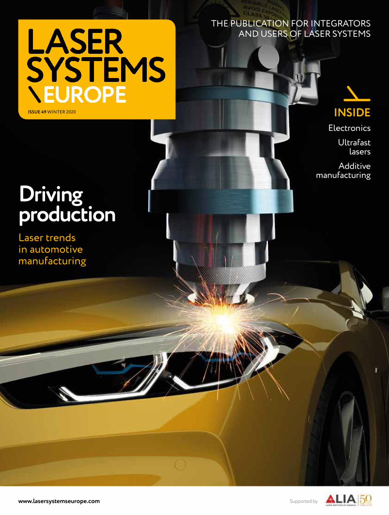
Driving productionLaser trends in automotive manufacturing

Participate in the premier event for the photonics and laser industries.
Plan to participate Photonics West
2021
6 – 11 March 2021 · spie.org/pw
The Moscone Center San Francisco, California, USA


We are Novanta
ARGES Cambridge Technology
SynradLaser Quantum
Novanta develops cutting-edge
components and sub-systems for
laser-based diagnostic, analytical,
micromachiningand fine material
processing.
Globally recognized Novanta brands
in Advanced Photonics.
For more information visit:www.novanta.com/
photonics

WINTER 2020 LASER SYSTEMS EUROPE 3WWW.LASERSYSTEMSEUROPE.COM | @LASERSYSTEMSMAG
Subscriptions: Free registrations available to qualifying individuals. Subscriptions £120 per year for four issues to readers outside registration requirements. Enquiries to Europa Science, 4 Signet Court, Cambridge CB5 8LA, UK. Tel: +44 (0)1223 221030. Fax: +44 (0)1223 213385. ©2019 Europa Science Ltd. While every care has been taken in the compilation of this magazine, errors or omissions are not the responsibility of the publishers or of the editorial staff. Opinions expressed are not necessarily those of the publishers or editorial staff. All rights reserved. Unless specifically stated, goods or services mentioned are not formally endorsed by Europa Science Ltd, which does not guarantee or endorse or accept any liability for any goods and/or services featured in this publication. US copies: Laser Systems Europe is published by Europa Science Ltd and distributed in the US by DSW, 75 Aberdeen Road, Emigsville PA 17318-0437. Periodicals postage paid at Emigsville PA. Postmaster: Send US address changes to Laser Systems Europe, PO Box 437, Emigsville PA 17318-0437.
Cover: medvedsky.kz gualtiero boffi/Shutterstock
Editorial and administrative team Managing editor: Greg Blackman [email protected] Tel: +44 (0)1223 221042Editor: Matthew Dale [email protected] Tel: +44 (0)1223 221047Advertising team Advertising manager: Jon Hunt [email protected] Tel: +44 (0)1223 221049 Production manager: David Houghton [email protected] Tel: +44 (0)1223 221034 Corporate team Managing director: Warren Clark [email protected] Systems Europe is published by Europa Science Ltd, 4 Signet Court, Cambridge, CB5 8LA, UK. Tel: +44 (0)1223 221030 Fax: +44 (0)1223 213385 Web: www.europascience.com l ISSN: 1759-0752
News 4Laser systems market could decline to $16bn l Researchers develop 10.4kW average power ultrafast laser l Additive firms launch printers with 10+ lasers l Sheet metal fabricator triples turnover during lockdown l Oil waste increases hardness of 3D printed aluminium
Feature: Electronics 8Keely Portway discovers how lasers are being used to advance Moore’s law, and how this technology could become more accessible to SMEs
Feature: Safety 12Lasermet’s David Lawton opens Matthew Dale’s eyes on modern challenges in laser safety
Interview: Automotive 16LSE speaks with Martin Kuhnhen about the usage of laser technology on automotive production lines
Analysis: Ultrafast lasers 18Stefan Janssen discusses the scanner-based laser processing technique developed within the Carbolase project
Analysis: Marking 20Simone Mazzucato discusses how lasers can be used to create hidden microfeatures in materials for anti-counterfeit purposes
Analysis: Machine learning 22 in additive manufacturing Brett Diehl puts neural networks to work in identifying voids in additive manufacturing
Analysis: Energy efficiency 24 in laser processing Nicholas Goffin investigates where energy savings can be made in laser processing
Analysis: Additive manufacturing 26Chao Wei and Lin Li discuss how different material properties could be integrated into single parts using additive manufacturing
AILU News 28Dave MacLellan on the transformation of ILAS into a digital conference
Products 29The latest equipment for industrial laser processing
LIA News 31Jana Langhans of LIA recaps this year’s ICALEO conference, which was held online for the first time in October
Suppliers’ directory 34Find the suppliers you need
This year has seen many conferences and events switch to an online format in the wake of the pandemic, with many organisers looking to continue this trend moving into 2021.
On page 28 Dave MacLellan shares how he intends to keep the networking opportunities of AILU’s ILAS conference alive next year, despite the event being held remotely. Meanwhile, on page 31, the LIA recaps its first digital ICALEO conference, which was originally due to be held in Chicago in October. To give you a taste of the event – which can still be viewed on-demand – the articles on machine learning in AM (page 22), and processing efficiency (page 24) have both been prepared by ICALEO speakers.
Many of you may have heard of the new A14 chip featured in Apple’s latest iPhone, which boasts 5nm transistors fabricated by ASML’s 180-tonne EUV lithography machine. On page 8, Keely Portway learns how affordable chip manufacturing tech is being developed by Fraunhofer ILT, for SMEs who don’t have $120m lying around to buy the latest system.
On pages 12 and 16 you can sit in on two very interesting conversations I had with experts on the topics of laser safety and automotive manufacturing, while on pages 18 and 20 you can read about some of the latest ways in which ultrafast lasers are being put to work in manufacturing.
We wish all our readers a safe and joyful end to the year and look forward to seeing many of you either digitally or in person in 2021!
Subscribe online for FREE at www.lasersystemseurope.com/subscribe
Systems online!
Matthew Dale, editor
LASER SYSTEMS EUROPE
Supported by the LIA
We are Novanta
ARGES Cambridge Technology
SynradLaser Quantum
Novanta develops cutting-edge
components and sub-systems for
laser-based diagnostic, analytical,
micromachiningand fine material
processing.
Globally recognized Novanta brands
in Advanced Photonics.
For more information visit:www.novanta.com/
photonics

4 LASER SYSTEMS EUROPE WINTER 2020 @LASERSYSTEMSMAG | WWW.LASERSYSTEMSEUROPE.COM
NEWS
The global market for laser systems for materials processing is expected to fall to $16bn in 2020, according to market research firm Optech Consulting.
This corresponds to a 10 per cent drop compared to the $17.9bn the firm reported for the year before.
The company also expects a decrease of around 10 per cent in the global market for industrial laser sources, with market volume expected to be close to $4bn for 2020.
‘The expected decrease for 2020 appears moderate, given the grim macroeconomic environment that developed under the impact of Covid-19,’ Optech Consulting said in its report. ‘The decrease also appears moderate when compared to the massive decrease of global sales of the machine tool industry this year.’
The demand of industrial lasers and laser systems follows the investment cycles of end industries, such as the 3C industry (computers, communications and consumer electronics), the mobile electronic devices industry, the automotive industry, as well as a broad range of end industries for major applications such as cutting and marking.
At the start of 2020, the industrial laser and systems market was in a continued downturn trend that began in mid-2018. This was reflected in the quarterly sales figures
LASERS IN ACTION
Laser systems market faces expected 10% decline to $16bn
of major industrial laser and system suppliers, such as IPG Photonics, Coherent and Han’s Laser. They showed a strong growth in 2017 followed by a decrease in the second half of 2018. This downturn was triggered by deteriorated economic expectations for major end industries, in particular the automotive and consumer electronics sectors.
With regards to China and its effect on the market, while the country had lead growth rates for several years, it decreased in 2019 due to the wide adoption of laser processes over a short time in the years prior.
This decrease also came with the above mentioned
deterioration in major end industries, trade conflicts, and the partial shift of foreign manufacturing investments to neighbouring countries.
However, 2020 quarterly sales of the major local laser and system manufacturers have recovered in quarters two and three from low first quarter levels, laying the ground for full-year figures which will exceed those of 2019.
“For Europe, North America and Japan, sales will be markedly down”
For Europe, North America and Japan, Optech Consulting expects that sales will be markedly down in 2020.
Microelectronics segment expected to growThe market for laser systems for microelectronics processing – for manufacturing semiconductors, flat panel displays, printed circuit boards and solar cells – had just started to recover from the downturn in 2019. This recovery was not halted by the pandemic, and demand for laser systems in the segment is expected to grow in 2020. But other segments in the industrial laser systems market are expected to decrease.
Overall, growth rates for single segments of the industrial laser market will encompass double-digit losses for lasers for standard systems, to positive growth rates for several segments of microelectronics processing.
Sitti
pong
Pho
kaw
atta
na/S
hutte
rsto
ck.c
om

A start-up sheet metal fabricator in Staffordshire, UK, has tripled its turnover and doubled its workforce since March.
Roo Engineering, which was started in April 2019 by husband and wife James and Abbi Rigby, has grown from an initial three employees to a workforce of 27, and now operates across two sites.
The firm specialises in metalwork and offers everything from design, finishing and assembly, to supply and installation. Its customers come from a variety of industries all over the UK.
The majority of the firm’s growth has occurred since the start of lockdown in the UK, when it secured a £1m contract for the manufacture of thousands of hand sanitiser dispensers.
So far this year the business has invested more than £500,000 in a new 6kW BySmart Fiber 3015 laser from Bystronic, as well as LED lighting that will help to reduce the company’s annual CO2 emissions by 15.45 and 3.1 tonnes respectively.
James, the managing director, told Business Live: ‘Our new laser has given us new capabilities, which will hopefully help us to win more work, and ideally, more locally-based contracts.
‘It will also mean we can create three or
Start-up sheet metal fabricator triples turnover during lockdown
four new positions in the next couple of months.’
Having been in engineering for more than 15 years, James saw the opportunity to set up his own business with Abbi using the contacts he had built up. ‘A lot of our growth has been organic,’ he said. ‘It’s only recently that we’ve started to really push things from a marketing perspective. Our plan is to continue to expand.’
WINTER 2020 LASER SYSTEMS EUROPE 5WWW.LASERSYSTEMSEUROPE.COM | @LASERSYSTEMSMAG
NEWS
Roo Engineering was founded by Abbi and James Rigby in April 2019
The international sheet metal working technology exhibition EuroBlech has been postponed once more, until 25 to 28 October 2022. The decision was taken in light of the ongoing pandemic.
ASML, a dutch manufacturer of chip-making equipment, has completed its acquisition of Berliner Glas Group, including all subsidiaries.
Blue diode laser manufacturer Nuburu has appointed a new CEO, Dr Guy Gilliland and a new CFO, Chris Baldwin, . The firm also recently raised $20m in Series B funding.
Laser manufacturer Luxinar has established a sales and service office in Shelby Township, Michigan, for its North American and Mexican customers.
The sales revenue of laser manufacturer Trumpf fell 8 per cent from €3.8bn to €3.5bn in the fiscal year 2019/20 ending 30 June. The firm also recently opened a €6m smart factory at its headquarters in Ditzingen, Germany.
SPI Lasers has taken on the name of its parent company. It now operates as Trumpf Laser UK.
IN BRIEF
Researchers have used carbon nanofibres derived from oil waste to increase the hardness of 3D printed aluminium products by 50 per cent.
The developed nanocarbon additive, obtained from the products of processing associated petroleum gas, could be used to improve the quality of 3D printed aerospace composites when added to aluminium powder.
The presence of even the slightest defects in printed structures is critical to the safety of the technology being created. According to the researchers, from The National University of Science and Technology in Moscow, the main risk of such defects is the
high porosity of the material, caused, among other reasons, by the qualities of the original aluminium powder.
To ensure a uniform and dense microstructure of printed products, the researchers proposed adding carbon nanofibres to the aluminium powder. The use of this modifying additive makes it possible to ensure a low porosity of the material, and an increase in its hardness by 1.5 times.
‘Carbon nanofibres have high thermal conductivity, which helps to minimise temperature gradients between printed layers during product synthesis, at the stage of selective laser melting,’ said
professor Alexander Gromov, head of the laboratory where the work took place. ‘Thanks to this, the microstructure of the material can be almost completely eliminated from inhomogeneities.’
The technology for the synthesis of nanocarbon
additives developed by the research team includes methods of chemical deposition, ultrasonic treatment, and IR heat treatment.
The used carbon nanofibres must be a by-product of associated petroleum gas processing. During its catalytic decomposition, carbon accumulates as nanofibres on dispersed metal particles of the catalyst. Usually, at present, associated gases are simply burned in the fields, which harms the environment. Therefore, the application of the new method also has a serious environmental significance.
The work was described in Composites Communications.
Oil waste used to increase hardness of 3D printed aluminium by 50%
NUST
MIS
IS
Busi
ness
Liv
e

6 LASER SYSTEMS EUROPE WINTER 2020 @LASERSYSTEMSMAG | WWW.LASERSYSTEMSEUROPE.COM
NEWS
Additive firms target serial production with metal 3D printers wielding 10+ lasersTwo additive manufacturing firms have unveiled metal 3D printers wielding at least 10 1kW lasers, intended for serial production.
SLM Solutions has commercially released the NXG XII 600, equipped with 12 1kW lasers, while Additive Industries has announced its development of the MetalFAB-600, expected in late 2021, which will operate with 10 1kW lasers.
The NXG XII 600The 12 lasers of SLM Solutions’ machine will operate simultaneously over a square build envelope of 600 x 600 x 600mm. Claimed by SLM Solutions to be the fastest machine on the market, the system operates up to 20 times faster than its single-laser system and up to five times faster than its four-laser system.
It is designed to be used in serial production for high-volume applications as well as for printing large parts, which is expected to open up new applications in the automotive and aerospace industries.
The new machine features a new optic system that enables large overlap and is based on a tailor-made laser scanning system to best fit the build area. All 12 optics provide spot-size definition via a double lens system called zoom function, which enables customers to choose between different spot sizes in the focal plane. The system will offer deposition rates of up to 1,000cm3/h and more.
To facilitate the integration of the NXG XII 600 into factories and supply chains, several
automated features, including an automatic build cylinder exchange, automatic build start, as well as an external preheating station and external depowder station, have been included as part of the solution.
‘Up until now, the limit had been considered to be that of a quad laser system,’ said Sam O’Leary, COO at SLM Solutions. ‘What we deliver here with 12kW of installed laser power is truly ground-breaking and a major step forward, not just for additive manufacturing, but for manufacturing in general.’
The MetalFAB-600Once released the MetalFAB-600 will offer a slightly larger build envelope of 600 x 600 x 1,000mm, while also being able to offer a deposition rate of up to 1,000cm3/h with its 10 1kW lasers. It will be developed on a platform that allows for even further expansion of the build volume and productivity in the future. The system’s powder handling, alignments, and calibrations will all be automated to ensure the highest possible output.
Airbus has validated the production of titanium aerospace components using a multi-laser 3D printer from GE Additive.
It enables single titanium components to be built at an increased rate in GE Additive’s Concept Laser M2 printer by using two lasers simultaneously.
This differs from a separate validation that took place in 2019, which enabled multiple components to be built in parallel in the printer, each manufactured by a single laser.
The new validation is significant for components that occupy much of the available space in the machine, which previously, due to their dimension, were not validated to be built at a faster rate using multiple lasers in parallel.
The process-critical area is where the exposure zones of the lasers overlap, also known as the stitching zone. The highest precision in the calibration of the optical systems and sophisticated compensation of, for example,
the influence of the process heat, is necessary to achieve the desired material properties.
‘With this advanced technology, we are now able to achieve a homogeneous, quasi-isotropic structure with excellent material properties in the overlap area, which does not show any discernible
differences from the previous quality standard,’ said Thomas Bielefeld, project manager of aerospace firm Premium Aerotec, who partnered with GE Additive to achieve the validation.
‘At the same time... we have succeeded in increasing productivity in component production by more than 30 per cent.’
Premium Aerotec will now use the newly validated system to produce components for the Airbus A320 family.
Airbus validates production of titanium components using multi-laser 3D printer
Researchers exceed 10kW average power with ultrafast fibre laser
Researchers have developed an ultrafast fibre laser with an average power more than ten times that of current high-power lasers. The technology could have applications in industrial-scale materials processing.
The laser, reported in Optics Letters, offers 10.4kW average power without degradation of the beam quality. This is particularly impressive as high-power ultrafast lasers can generate waste heat exceeding 1kW average power, which has been known to degrade the beam quality. To circumvent this, the researchers created the laser by externally combining the output of 12 laser amplifiers. Thermographic imaging of the final beam combiner revealed only marginal heating.
According to the researchers, from the Friedrich Schiller University, Jena, and the Fraunhofer Institute for Applied Optics and Precision Engineering (IOF), power scaling to the 100kW level could be achieved by adding even more amplifier channels.
The investigation of novel applications at that power, and transfer of the laser technology to commercial systems is ongoing within the frame of the Fraunhofer Cluster of Excellence Advanced Photon Sources, which involves engineering the laboratory setup into a rugged design. On the research side, the team in Jena is focused on multicore fibres with potential to deliver superior performance in simpler and smaller systems.
SLM
Sol
utio
ns
Prem
ium
Aer
otec
TURNKEY LASER MACHINES
From medical devices to electronics, automotive to packaging, consumer goods to jewelry—our turnkey laser machines enable you to achieve greater efficiency, higher speed, and reduced cost of operation.
Learn more at coherent.com/machines-systems
lasermet.comlasermet.com+44 (0) 1202 770740 [email protected]
glaser jailer
• Laser Safety Interlock® Control Systems
• Integrated and Certified Laser Protection Equipment
for Automation and Processing
Modular, Cost Effective, Laser Safety Cabins
liding oorsby torm
a Lasermet productionActive Laser Safety Filter Windows
™
TURNKEY LASER MACHINES
From medical devices to electronics, automotive to packaging, consumer goods to jewelry—our turnkey laser machines enable you to achieve greater efficiency, higher speed, and reduced cost of operation.
Learn more at coherent.com/machines-systems

Keely Portway discovers how lasers are being used to advance Moore’s law, and how this technology could become more accessible to SMEs
@researchinfo | www.researchinformation.info
Moore’s Law came into being more than 50 years ago, when a research specialist at American semiconductor company, Fairchild Semiconductor, suggested that the number of transistors in dense integrated circuits could double every two years.
That specialist, Gordon Moore, consequently predicted that the speed and capability of computers would also increase every two years. Moore’s prediction has since been used in the semiconductor world for planning and product development, and has been a near-reality ever since. This has been driven by advances in photolithography, one of the key technologies behind size reduction of computer chip components.
While there is not a definitive consensus about when, or if, Moore’s law will come to an end, there has been speculation that semiconductor advancement has slowed in the past 10 years. However, in the last two years, manufacturers of this technology have developed new, mass-fabrication practices, for which lasers play a crucial role.
Some recent market predictions appear to dispute the slowing of semiconductor development altogether. The Semiconductor Industry Association recently announced that global sales of semiconductors totalled $113.6bn in the third quarter, an increase of 11 per cent on the previous and a 5.8 per cent increase year-on-year. Looking ahead, Technavio’s Global Semiconductor Market 2020-2024 report forecasts that the global market size will grow more than $90bn by 2024.
Driven by 5GTechnavio’s report states that major market growth came from the integrated circuits
segment last year, which is expected to experience the fastest growth during the next five years, largely because of the growing investments in telecommunication network deployments, including 5G networks.
The most recent, and arguably one of the most famous, examples is the iPhone 12. The new smartphone features what Apple calls the world’s first processor built from 5nm transistors: the A14. The processor was supplied to Apple by Taiwan Semiconductor Manufacturing Company (TSMC), for use in its smartphones, tablets and Mac computers. It is anticipated that the transistors – which are about the width of 25 atoms – will also begin to appear in some of the leading PCs, servers and
smartphones from multiple vendors in the next year.
To put the size of the transistors into context – and return to Moore’s Law – there are about 171 million of them laid out over every square millimetre of the chip. This has been possible thanks in no small part to Dutch firm ASML.
The lithography system manufacturer developed a technique to carve circuitry patterns into silicon via extreme ultraviolet (EUV) lithography – and this is where lasers earn their stripes. Back in 2018, laser manufacturer Trumpf described at Epic’s Executive Meeting on Industrial Lasers how it was using CO2 lasers to develop EUV lithography systems for this purpose. Dr Andeas Popp, a project head at Trumpf Photonic Components, explained that this new application of CO2 lasers will be key for taking the next step in Moore’s law. This is because the size of semiconductor structures on chips are approaching atomic dimensions – something that has been made possible by complex exposure processes enabled by lasers.
To the limitPreviously, exposure processes had been performed using UV radiation generated by 193nm excimer lasers. But this wavelength range faces limitations when producing
UPHOLDING THE LAW
8 LASER SYSTEMS EUROPE WINTER 2020 @LASERSYSTEMSMAG | WWW.LASERSYSTEMSEUROPE.COM
FEATURE: ELECTRONICS
“The cost of the systems is exorbitant right now and it is not going to become cheaper any day soon”
The EUV source at Fraunhofer ILT’s Excimer facility delivers 40W at 13.5nm
Frau
nhof
er IL
T

g
structures less than 10nm in size. For structures in the range of 5nm, exposure at shorter wavelengths in the EUV range must be used to provide the resolution necessary for their fabrication.
Trumpf collaborated with ASML, its subsidiary Cymer and optics giant Zeiss, to develop the systems. The EUV lithography technology quickly generated interest from major semiconductor manufacturers, according to the company, with such end-
users placing orders for the systems, to ramp up their mass production throughout 2018 and 2019.
TSMC was one such company, and is now sole supplier of the A14 processor to Apple. Samsung is also putting the technology to good use, and is set, alongside Qualcomm, to imminently reveal a new processor for Android phones. Then there is Intel, which is reportedly looking to start using the technology next year.
Counteracting the costBut what about start-up companies, or those of a smaller or medium size (SMEs)? The ASML machines cost in excess of $120m (£90m) each, which is high even compared with other semiconductor industry tools.
This has led many speculators to argue that, because the cost of a single EUV layer on a chip is about three times the cost of a layer that uses traditional processing, this
WINTER 2020 LASER SYSTEMS EUROPE 9WWW.LASERSYSTEMSEUROPE.COM | @LASERSYSTEMSMAG
FEATURE: ELECTRONICS
Frau
nhof
er IL
T
Fraunhofer ILT has spent the past four years heading up the completed EU project ADIR, which saw lasers being used to process electronics at the end of their lifespan.
The project was launched with the aim of developing a completely new, sustainable and automated method of recycling electronic devices by disassembling them and recovering the valuable raw materials they contain.
It’s eight partners from three countries sought to reduce the EU’s dependency on natural resources, cut the need for costly imports of raw materials, and demonstrate technologies for inverse production.
The new recycling concept focuses on the elements tantalum, neodymium, tungsten, cobalt and gallium. Found in virtually every modern electronic device, these metals are valuable due to their scarcity, their cost – which in some cases is close to €250/kg – and the tremendous difficulty of recovering them from used
electronic devices in a cost-effective way.
The disassembly method relies on an intelligent combination of laser technology, robotics, vision systems and information technology. Lasers are used to perform key tasks such as identifying what each component consists of, as well as desoldering or cutting components out of the board in a fast, non-contact process.
The procedure was proven to be an efficient way to recover strategically important materials of high economic value on an industrial scale. ‘We disassembled around 1,000 mobile phones and more than 800 large computer printed circuit boards, from which we recovered several kilograms of components for recovery,’ confirmed ADIR’s manager Dr Cord Fricke-Begemann. ‘We were able to gain between 96 and 98 per cent of the tantalum.’
With the project now being completed and the concept’s economic viability proven, the
partners have already attracted interest from industry – having found an initial set of partners willing to put their methods into practice, while continuing to seek further candidates.
The advantages of the new recycling concept go beyond a more efficient use of raw materials. According to Fraunhofer ILT, it has the potential to reduce Germany’s dependence on shipments of raw materials from other regions, by offering new opportunities to introduce
inverse production technologies. These are required to establish closed material cycles for a future sustainable economy.
There is still room for improvement in the concept, however. According to the project partners, smart automation concepts could be used to speed up the dismantling processes for the housing of mobile phones to get access to the printed circuit board, the battery and magnetic components.
NEXT-GENERATION URBAN MINING
Lasers can recover valuable raw materials from end-of-life devices
Frau
nhof
er IL
T
Frau
nhof
er IL
T
At Fraunhofer ILT, a laboratory system for EUV has been built to process wafers with a diameter of up to 100mm
Nanostructures with 300nm (left) and 28nm (right) half-pitch, created using DUV and EUV technology respectively

g cancels out the benefits of transistors this size.
Moreover, Moore’s Law historically yielded 40 per cent reductions in transistor cost, but the benefit from this new technology will be closer to around 10 per cent. In addition, by prohibiting smaller businesses and start-ups from accessing the technology, the cost could also prevent more new and exciting developments reaching the market.
To help counteract this problem, Fraunhofer ILT is developing technologies for the production of nanostructures that start-ups or SMEs can also afford. The idea, revealed Dr Serhiy Danylyuk, team leader of EUV and DUV technology at the institute, is to generate periodic structures via the interference effects of coherent radiation, like the achromatic Talbot effect. In the near field – less than 500µm behind a mask – an intensity distribution is created with which microlithographic structures can be produced.
Danylyuk explained: ‘The cost of the systems is exorbitant right now and it is not going to become cheaper any day soon. So, we got thinking that we could try to scale down and make it possible for SMEs.’
Scientists at the institute are doing this using a KrF excimer laser at a wavelength of 248nm to generate structures with a period of several hundred nanometres. This was tested with a Leap150K laser system from Coherent. In a photoresist, 180nm wide lines can be generated with a period of 600nm. With higher energies of 250mJ/cm², silicon on glass can also be ablated with similar dimensions. The technology is also well suited for the ablation of PET plastic surfaces on a 300nm scale.
The principle also works with wavelengths in the EUV, as used to produce the 5nm transistors. The institute developed its own beam source for this purpose, the FS5440. This is based on a gas discharge, and can generate the required radiation at 13.5nm
wavelength. It is also much more compact than the laser-based EUV source used in large-scale industrial facilities.
‘There are three main cost factors in EUV technology,’ continued Danylyuk, ‘the point of source; the optical system, which is extremely expensive and technologically advanced in the large scale; and, of course, the positioning system, which places high demands in the nanometre range. We thought that smaller laser sources would be
the best thing. We are basically happy to use any kind of source, depending on customer requirements, but we believe our own plasma source to be the cheapest.’
Masks or mirrors?Transmission masks were used as an alternative optical scheme to reduce the amount of mirrors required in the system.
‘We worked on a simpler scheme, using transmission masks not as expensive as mirrors,’ said Danylyuk. ‘We developed these in-house and it means we can use maybe one or two mirrors in the system, not nine. This is not necessarily as scalable as using reflective masks, but if you are an SME going for smaller volumes, this approach could work. The mask is positioned in the vicinity of the wafer, and we can demagnify the structure by a factor of two.’
In terms of cost, while Danylyuk acknowledged that, while it may never reach the thousand-dollar mark, the system under development will still be significantly more accessible than those currently available. ‘I think we will be looking at low six numbers,’ he said. ‘It depends on the requirements on the source side.’
Discussing the challenges of working toward such a technology – which has been in development at Fraunhofer ILT for almost 10 years – Danylyuk said: ‘It’s probably hard to go to the resolution of 5nm and below with this technology, but we are looking at a sub-20nm scale already, and whether SMEs need such a small resolution. It should be scalable to 10nm but it’s challenging, both from a mass-manufacturing and a positioning point of view. Systems have to become more expensive if you want to drive to single nanometre precision. Somewhere we need to make a cut and say “that’s perhaps not what SMEs would need anyway”.’
An additional challenge for the institute came with the positioning of the mask. ‘We had to position it in a sub-millimetre distance to the wafer, and make sure that the distance is maintained over the full wafer size,’ said Danylyuk. ‘So we developed a technology for maintaining dynamic distance. Our system is currently working with 100mm wafers, and there is no reason why it cannot go larger, but the medium size is what many of the SMEs are comfortable with, and there is a lot of technology available for this wafer size.’
Ready and waitingSo, how do SMEs get their hands on this technology? ‘Everyone is welcome to use our facility to test this technology,’ said Danylyuk. ‘Depending on the end-use, we can also speak with our partners about how to bring the technology to the market. This way, people can get an idea of whether it is suitable for them, and what kind of effort is needed to bring it into their facility.’
It is also worth noting if, after taking these steps, SMEs still feel that the technology is out of their reach, there are other options available. ‘If the cost is still too high, they could consider using far ultraviolet (FUV) as the laser source,’ said Danylyuk. ‘It uses a similar technology and the same type of approach that we use in EUV, but with FUV – and this may not give you the sub-10nm structures, rather 100 to 150nm – the technology is more scalable by using commercially available UV laser sources.
‘So, for people who may only need to use structures on the scale of under 200nm, with different materials, we can offer the development of lithography-based UV, and also direct laser structuring technology.’ l
10 LASER SYSTEMS EUROPE WINTER 2020 @LASERSYSTEMSMAG | WWW.LASERSYSTEMSEUROPE.COM
FEATURE: ELECTRONICS
“Fraunhofer ILT is developing technologies for the production of nanostructures that start-ups or SMEs can also afford”
The iPhone 12 features the world’s first processor built from 5nm transistors, thanks to laser technology
Appl
e

www.scanlab.de
precSYS 515: Scan System forChallenging Micro Machining Applications
• Optimized for 515 nm ultra-short pulse lasers
• Processing of flexible geometries with high aspect ratios
• Smallest spot size for more precision
Five Axes and a Green Laser for Finest Structures
NEW
22” Diameter • 1/20 wave PV TWE and betterAbsorption measured < 25 PPM @ 1064nm
Large C-plane available • No thickness restrictions
45+ YEARS OF HEM GROWTH EXPERTISE
GTAT.com | 978-745-0088 | [email protected]
The Clear Choice for Large Optical Sapphire
HEM Sapphire
PHOTOPTICS 20219th International Conference on Photonics, Optics and Laser technology11-13 February, 2021Online Streaming
Keynote speakers
Dieter Bimberg, Bimberg Chinese-German Center for Green Photonics of the Chinese Academy of Sciences, CIOMP and Center of Nanophotonics, TU Berlin, GermanyJean-Jacques Greffet, Laboratoire Charles Fabry, Institut d’Optique Graduate School, Université Paris-Saclay, FranceEnzo Di Fabrizio, Polytechnic of Turin, ItalyGershon Kurizki, Weizmann Institute Of Science, Israel

Lasermet’s David Lawton opens Matthew Dale’s eyes on modern challenges in laser safety
@researchinfo | www.researchinformation.info
‘Almost everyone looking to use lasers for materials processing should be looking to use a Class 1 laser product.’
That’s David Lawton’s view, as he sat down with me to talk ‘the latest in laser safety’.
The statement raised a number of questions, as despite being the editor of an industrial laser magazine, embarrassingly I was not fully up to scratch with my laser safety terminology.
This is why I stopped Lawton immediately and let my curiosity get the better of me: ‘What does that term actually mean David: “Class 1 laser product”?’
While writing for Laser Systems Europe has taught me that you won’t find a materials processing laser lower than Class 4, I’d never actually stopped to think about what each class defines exactly.
Lawton was more than happy to indulge me, however.
‘The four classes of lasers have been determined based on each one’s ability to cause harm to the human body.
‘Class 1 lasers are totally and unconditionally safe, there is no way they can cause human harm – think of a barcode scanner in a supermarket;
‘Class 2 lasers are visible lasers that, while being able to cause damage to the eyes, take longer than a quarter of a second to do this – in which time your body’s natural reflexes will either close your eyelids or
move your head out of the way of the beam before any damage can be done;
‘Class 3 lasers can be of both visible and invisible wavelengths and the beam or (specular) reflected beam can damage the eye or skin quicker than a quarter of a second. The diffused or scattered radiation of a Class 3 laser, however, is safe, as it does not pass the eye/skin damage threshold. In other words, they are only dangerous if you are in direct contact with the beam, looking at the spot itself will not cause harm.
Class 4 lasers however are able to cause damage with their reflected or scattered radiation – you can’t even look at the spot. This of course depends on the wavelength and power of the laser, divergence of the beam etc, but it could be dangerous.’
I was slightly alarmed when he explained that the power level of Class 4 lasers, rather than starting at hundreds or even thousands of watts, begins at no more than half a single watt. In case, like me, you need it pointing out, that means that while Classes 1, 2 and 3 cover anything up to 499mW, technically, a 500mW laser and a 100kW laser can belong in the same class when it comes to their ability to harm a human.
‘I feel like there should be at least a fifth class in there somewhere David.’
‘You’d be right in thinking that,’ he said, ‘and the potential creation of Class 5 is something that is being discussed, however where could the line be drawn for this? There’s an
argument that suggests that: “if no PPE exists that can protect you from this laser, then that should be Class 5”, however for the moment, the general consensus is that everything that could do that is still in Class 4.’
With the class system covered, that brought Lawton to the second half of the term I queried: ‘laser product’.
‘During normal operation, a Class 1 laser product will never expose the user to anything above Class 1 levels of radiation,’ he explained. ‘A great example is a Blu-ray player. This is a completely safe product that anyone can use without safety training, a risk assessment, signs outside the door etc. However it contains a Class 3 laser, meaning as soon as you open it up, you put yourself at risk.’
An interesting example, I thought, but how does this come into play in industrial materials processing?
This is where Lawton introduced his and Lasermet’s quite elegantly simple mantra: ‘put it in a box’.
Behind closed doorsThe ‘put it in a box’ school of laser safety – as Lawton said it is colloquially known – is
BOXING UP THE BEAM
12 LASER SYSTEMS EUROPE WINTER 2020 @LASERSYSTEMSMAG | WWW.LASERSYSTEMSEUROPE.COM
FEATURE: SAFETY
“The potential creation of Class 5 is something that is being discussed”
Left: diagram of a laser enclosure containing a robot designed to build propellers. Right: the enclosure in use live at a trade show thanks to its Class-1 laser product status

g
about creating an environment where no harmful radiation can escape and where no human can enter while a laser is active.
‘Why should you have to wear PPE if you can simply contain a laser in a controlled environment? Even the UK’s Health and Safety Executive (HSE) is starting to get in line with this way of thinking, advising people to “enclose laser radiation where possible”.’
This is in no way a new line of thinking. As in materials processing, there are very few lasers with which you can even stand in the same room. As a result, nearly all materials processing lasers are either contained in a laser machine, or instead have an enclosure erected around them, armed to the teeth with interlocked doors, active guarding, safety windows and bright LED signage.
‘Laser safety is about understanding the hazards, containing those hazards and making sure that nobody is exposed to them,’ continued Lawton. ‘This is why the “put it in a box” methodology is so elegant, because with it, laser safety isn’t actually that difficult. It can apply to anything from a small multi-watt laser on a tabletop, through to a turnkey system containing a kilowatt laser, and even on to, for example, a colossal enclosure that can take a part as large as an aircraft wing and process it using a multi-kilowatt laser.’
In this example, according to Lawton, the interlock-equipped enclosure could be made to have the same Class 1 laser product status as the aforementioned Blu-ray player.
‘The enclosure would have to be tens of metres in length, depth and height to contain such a process of course, but it could be done,’ he confirmed.
What Lawton said next enabled me to openly admit my lack of laser safety knowledge at the start of this article. I’d previously been under the impression that everyone involved in laser materials processing – besides myself of course – was well-versed in laser classes and what exactly a ‘Class 1 laser product’ was. This apparently isn’t the case, however.
‘So many times we’ve had to go to customers because they’ve bought a Class 4 laser when they should have just purchased a Class 1 laser product,’ he revealed. ‘For example one customer bought a Class 4 laser to mark parts on a production line. The manufacturer of the laser was under no obligation to tell the customer “by the way, because you now have a Class 4 laser in your organisation, you’ll have to perform a risk assessment, appoint a laser safety officer and provide additional training for your users.” If that customer had been savvy and instead just
purchased a Class 1 laser product, they wouldn’t have had to do any of that in the first place.
Not as simple as it seemsWhile ‘put it in a box’ does somewhat simplify laser safety from a user perspective, the same cannot be said for those actually making the ‘box’.
Before I continue, those reading should first know that the cost-per-watt of lasers has dropped dramatically in the past 15 years.
‘Even within this decade lasers have been seen as a monster investment,’ said Lawton. ‘For example, one of our customers bought
WINTER 2020 LASER SYSTEMS EUROPE 13WWW.LASERSYSTEMSEUROPE.COM | @LASERSYSTEMSMAG
FEATURE: SAFETY
Lase
rmet
“Many times we’ve had to go to customers because they’ve bought a Class-4 laser rather than a Class-1 laser product”

g a 10kW laser a while ago for a whopping £1m. They’ve since bought a 30kW laser for less than that.’
Combined with the advent of fibre laser technology, this lowering cost has enabled lasers to be used increasingly for remote welding. ‘Previously, when CO2 lasers were the standard, welds would be performed at a 50 to 100mm standoff from the workpiece, using a system of mirrors to deliver the beam,’ said Lawton. ‘Fibre lasers enable the beam to be sent along an optical fibre and down a robotic arm, which combined with developments in optics enables remote welding to be performed up to distances of well over a metre. I have seen a laser 1.8m away from the focal point in such an application!’
For that setup, Lawton explained, it would mean that even 1.8m past the focal point of the laser, the power density could be the same as it was when it originally came out of the optics – spread over a diameter of approximately 20mm.
‘The power density is still dangerously high away from the focal point, which from a safety perspective brings a whole new level of risk,’ he remarked. ‘Remote welding is a real challenge. While the whole process can still be put in a “box”, you have to determine whether the box is good enough to stop the beam. This will determine what sort of enclosure is required and what that enclosure will be made of.’
In testing enclosures, Lasermet has to fire lasers of different powers and spot sizes at its guarding to determine how quickly they burn through it. A protective exposure limit (PEL) rating is then given to the product. ‘You can then calculate the foreseeable exposure limit (FEL) on the guard, so we know how the laser will interact with it,’ Lawton explained. ‘As long as the FEL is below the PEL for the time required, then the guard will stop the beam, otherwise, the beam will burn through.’
In addition to accounting for various beam divergences and their intensities when building an enclosure for remote welding,
Lasermet also has to consider what happens if the laser spot is reflected directly during processing, which is known to happen, according to Lawton: ‘Welding metal creates a molten pool that, due to surface tension, can sometimes act as a perfect reflector and bounce a powerful spot of radiation onto a guard, screen or wall.’
As a result, the firm has to presume the worst when building a laser safety enclosure: what happens if the laser gets locked in position, striking a wall directly at maximum intensity?
Children running the sweet shopThanks to the ‘worst case scenario’ measures taken by system and enclosure manufacturers, despite the dangers that lasers pose, owners of Class 1 laser products can have peace of mind that their laser is locked away safely behind closed, interlocked doors... right?
Not necessarily, as I soon found out thanks to Lawton’s final and rather shocking point: that anyone can self-certify a Class 1 laser product, and that most companies do just that.
This baffled me. To know that rather than being regulated and controlled by a governing body, the certification of a system containing a Class-4, multi-kW laser as a ‘Class 1 laser product’, has most likely been done by the system’s manufacturer.
‘It’s quite common for manufacturers to self-certify,’ said Lawton candidly. ‘Even the largest and most respectable laser firms
do this...“children running the sweet shop”, I call it!’
He quickly gave evidence to show that this remark was not unwarranted: ‘I have seen a UK company buy a laser product from a US firm, and the sources that the US manufacturer said were inside the device were not the sources in the delivered product. What had happened was that the US manufacturer had changed the sources a few years prior and not actually changed the product’s classification. This device went from being an eye-safe product to a non-eyesafe product, and had been sold worldwide.’
Asking Lawton why there hasn’t been any move towards legislatively controlling laser product certification, he said that such a question had indeed been raised before at an annual laser safety forum in which he takes part. ‘The argument that came back was that there are many other aspects of products, for example regarding electromagnetic compliance, the low voltage directive etc, that are listed in a declaration of conformity – almost all of which can be self-certified.’
Seeing that I wasn’t convinced that such an argument was strong enough to justify a lack of legislative control over laser certification, Lawton asked rhetorically: ‘Is it right that a manufacturer can say ‘this is a “Class X” laser product, and you’ll just have to take my word for it?’
While Lasermet was accredited by the UK’s National Accreditation Body (UKAS) in July, which enables it to test the safety of customer’s laser equipment in-situ to the laser safety standards BS EN 60825-1:2014, 2007, 2001, such independent tests are not yet compulsory by law.
I’d like to think that this could one day change. However, if any of you out there can convince me otherwise as to why this would not be a good idea, feel free to voice your thoughts in an op-ed for our next issue: [email protected] l
14 LASER SYSTEMS EUROPE WINTER 2020 @LASERSYSTEMSMAG | WWW.LASERSYSTEMSEUROPE.COM
FEATURE: SAFETY
“It’s quite common for manufacturers to self-certify... ‘children running the sweet shop’, I call it!”
Left: a large laser welding enclosure in use at the Manufacturing Technology Centre in the UK. Right: inside the laser welding enclosure
David Lawton is European sales manager at Lasermet
Cya
n-Te
c

LASER SAFETY –A MATTER OF TRUST
www.blz.org/laser-safety
Virtual Laser SafetyTraining & Consulting
In the fields of laser material processing, measurement technology, optical fibrecommunication systems, medical and cosmetic laser applications
We are experts for- Training of laser safety officers- Individual trainings considering company specific issues- Laser safety consulting- Testing of laser safety products
You can trust in- More than 20 years experience in laser safety- High quality trainings according to European standards- Confidentiality due to own meeting server
Visit us on our website and learn more about our laser safety services.
Photo: K. Fuchs / blz

We ask Martin Kuhnhen, head of Jenoptik’s Light & Production division, about the usage of laser technology on automotive production lines
@researchinfo | www.researchinformation.info
Jenoptik has recently won a major order for three automated production lines from Gestamp, a manufacturer of metal automotive components. The firm’s light and production division will design, manufacture and integrate the three lines, each of which will use different welding and laser cutting technology to help manufacture complex car body parts for electric vehicles.
We caught up with division head Martin Kuhnhen, to ask how laser technology is being used on such production lines, as well as how established it is as a manufacturing tool in the automotive industry.
What led to Jenoptik becoming an integrator of automotive production lines?Historically Jenoptik has been in the business of standalone machines. This is because laser processing used to be conducted in such machines via individual logistics – mostly manual, sometimes with gantry solutions. Nowadays laser processing is much more integrated into production lines.
Jenoptik’s light and production division has acquired a few automation integration companies in North America and Spain over the past three years. We did this because we saw that there is an increasing demand for end-to-end processes from automotive manufacturers and their suppliers. Lasers are just one part of these processes, meaning that such customers are also requesting that pre- and post- laser processes are included in their production lines as well.
For example, if a production line was producing complete doorings for vehicles from press-hardened steel: while laser cutting and welding are important parts of that line, there are also conventional
welding and assembly jobs before and after these processes. Historically, automotive firms have had to manage several suppliers working on different pieces to bring all of this together, which can introduce logistical and timing issues.
If one entity is able to provide the equipment for all of these processes, then this takes a big headache away from manufacturers. With the disruptive change in the automotive sector, the industry is focusing on other topics now, so everyone is happy to find suppliers that can take these traditional headaches away.
Could you elaborate on this ‘disruptive change’ in the automotive sector?This refers to, for example, the fact that the automotive industry is currently having to manage the transition from conventional engines to e-mobility, the introduction of autonomous driving, or having to follow customers to Asia. There are several trends, all happening in parallel, which keeps automotive firms very busy compared to previous years.
In addition, the core competencies of automotive firms are shifting. We are seeing more and more automotive firms saying that manufacturing is no longer their most important core competence. Consequently, they need to find reliable partners to address this part of their business. This is because they still have to meet deadlines
and achieve the required volumes for a runoff of a production line. Whereas automotive firms used to manage that very well themselves, they are now trusting more and more in strategic partners to do this.
Jenoptik now considers the integration of production lines to be one of its core competencies. On a customer-specific programme basis, we select the right combination of components, bring them together and manage them with the right software. It is no longer just producing standalone machines. We use our own laser modules, products and software to enhance standard components from the market and secure the necessary performance.
How are lasers currently being used for manufacturing in the automotive sector, what makes them suited for this purpose?Lasers are used to cut vehicle doorings, ABC pillars or really any structural part in a car body made out of press-hardened steel. They are preferable, as they offer a wear-less process – alternative mechanical tooling would wear out very quickly. This is a major market for laser processing, with many parts now coming into this corner. Lasers are also increasingly being used to cut and trim aluminium castings, such as domes, cross members, rear lids and also plastic parts – both on the interior and exterior of a vehicle.
In addition to welding and cutting,
LIGHT ON THE LINE
16 LASER SYSTEMS EUROPE WINTER 2020 @LASERSYSTEMSMAG | WWW.LASERSYSTEMSEUROPE.COM
INTERVIEW: AUTOMOTIVE
Gestamp’s new Jenoptik production lines will each use different welding and laser cutting technology to help manufacture complex car body parts for electric vehicles
Jeno
ptik

Jenoptik’s production lines perform applications such as laser marking and scoring. Airbag scoring, for example, is implemented on driver airbag covers and instrument panels on the passenger’s side. It has to be very precise and reliable and produce a defined break-line in such material, which allows the airbag to explode through its cover material, but only when it should, on impact. In addition, when welding components for e-mobility, for example in batteries, extreme precision is also required, as you are processing components next to explosives.
Lasers also introduce a lot of flexibility to automotive manufacturing. For example if you were producing bumpers, some might require parking sensors, while others will not. Whereas previously individual machines would have been required for each bumper configuration, now they could all be run through a single laser machine in a one-piece flow logic. In addition, automotive manufacturers would have to runoff production lines for producing new vehicles, while keeping old equipment to produce spare parts for previous vehicles. A laser machine can instead be used to produce spare parts when required, while mainly processing parts for new vehicles, minimising disruption.
Lasers will also move into new application
areas in the automotive industry. We are engaged in a couple of research programmes focusing on applications where new functionality is being introduced into parts. For example, there are exterior parts for autonomous vehicles that have special lighting functionality built in, allowing the vehicle to signal to pedestrians and tell them ‘I see you’, when a pedestrian wants to use a road crossing. In producing such parts, lasers play an important role. Such products will be seen on the streets in the next 12 to 18 months.
We see that process monitoring and AI is gaining increasing interest in the automotive sector. Why?Process monitoring is required as the materials brought into a production line have different tolerances. If output is to be increased, materials have to be measured and inspected at the beginning of the production line, then parameters have to be changed on the fly when materials of different tolerances are introduced.
Previously, you would have had to take these out and say ‘I can’t process them’. Now you can adjust parameters constantly, which is enabled by AI and other software-based features for process monitoring.
The inclusion of AI and process monitoring in production cells is certainly an increasing demand among our customers. For example, we also sold a complex line for cutting metal tubes for automotive e-drive support frames that used AI to adjust the specific cutting position by analysing the introduced material. This is a relatively new trend and we see that AI for camera-based process monitoring – both pre- and post- process – will increase in the future.
The path going forward is definitely to enhance laser capabilities with more camera
based inspection and AI usage in order to make the adjustment of process parameters easier on the fly. That will be a big step going forward.
Do many more automotive firms still need to make the switch to laser technology?Certainly. In the automotive industry, a large number of manufacturers still need to adopt laser processes. If you take laser cutting of press-hardened steel for example, three automotive suppliers currently dominate the market. They process approximately 70 per cent of all the parts. Why is that the case? Because laser processing is a complex process. They invested early in the game and increased their knowhow. By taking on the whole integration process ourselves, firms like Jenoptik can reduce the barriers to adopting laser processing, enabling more and more smaller automotive manufacturers to ‘join the family’, as it were.
Lasers in the visible wavelength are increasingly considered for e-mobility fabrication. Will Jenoptik keep an eye on this technology?We appreciate the technical benefits of green or blue lasers when welding material like copper or aluminium, and in general, we are open to integrate them in our automation lines if specified.
Nevertheless, our automotive customers are clearly addressing the economic aspect as well, and here infrared single-mode laser sources, combined with intelligent process parameters and laser beam shaping, have major benefits, while providing very acceptable application results.
Do you believe other manufacturers of laser equipment will shift to also become integrators?Most of the laser industry is still focusing on individual processing heads, laser sources or turnkey systems. However, we clearly see the automation and integration of laser technology will become a trend. We constantly improve our own competence to stay ahead of the game, and have received very positive feedback from our customer base already.
The three production lines we are currently producing for Gestamp, which include 20 laser cutting modules, represent a significantly larger volume for Jenoptik, in comparison to our traditional projects. l
WINTER 2020 LASER SYSTEMS EUROPE 17WWW.LASERSYSTEMSEUROPE.COM | @LASERSYSTEMSMAG
INTERVIEW: AUTOMOTIVE
Lasers can be used to cut vehicle doorings, ABC pillars and any other structural part in a car body made out of press-hardened steel
“Core competencies of automotive firms are shifting... more and more say manufacturing is no longer their most important core competence”
Stefan Janssen, of Fraunhofer ILT, discusses the scanner-based laser processing technique developed in the Carbolase project
@researchinfo | www.researchinformation.info
ITA
Scan
lab
Co-authored by Dr Sebastian Oppitz, of the Institut für Textiltechnik at RWTH Aachen University, and Dr Matthias Morasch, of Scanlab
Fibre reinforced polymers (FRPs) are particularly popular materials for manufacturing products that are subject to strict weight and durability requirements, such as in the automotive and aerospace industries. Carbon fibres are a common choice for these kinds of applications, where they are referred to as carbon fibre reinforced polymer (CFRP) elements, or simply ‘carbon fibre’. The bonded fibres are incredibly strong and stiff, but at the same time they are extraordinarily lightweight. However, they are both expensive and difficult to process. Joining CFRPs to other components creates unique challenges that manufacturers must overcome.
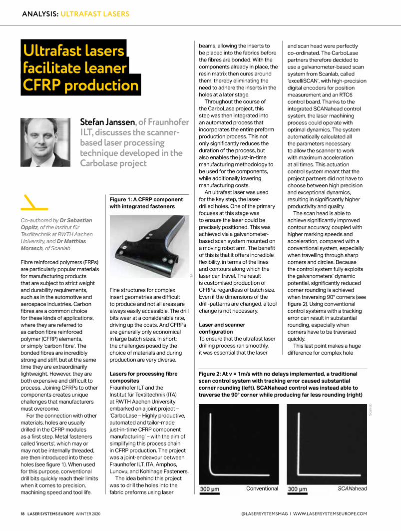
For the connection with other materials, holes are usually drilled in the CFRP modules as a first step. Metal fasteners called 'inserts', which may or may not be internally threaded, are then introduced into these holes (see figure 1). When used for this purpose, conventional drill bits quickly reach their limits when it comes to precision, machining speed and tool life.
Fine structures for complex insert geometries are difficult to produce and not all areas are always easily accessible. The drill bits wear at a considerable rate, driving up the costs. And CFRPs are generally only economical in large batch sizes. In short: the challenges posed by the choice of materials and during production are very diverse.
Lasers for processing fibre compositesFraunhofer ILT and the Institut für Textiltechnik (ITA) at RWTH Aachen University embarked on a joint project – ‘CarboLase – Highly productive, automated and tailor-made just-in-time CFRP component manufacturing’ – with the aim of simplifying this process chain in CFRP production. The project was a joint-endeavour between Fraunhofer ILT, ITA, Amphos, Lunovu, and Kohlhage Fasteners.
The idea behind this project was to drill the holes into the fabric preforms using laser
beams, allowing the inserts to be placed into the fabrics before the fibres are bonded. With the components already in place, the resin matrix then cures around them, thereby eliminating the need to adhere the inserts in the holes at a later stage.
Throughout the course of the CarboLase project, this step was then integrated into an automated process that incorporates the entire preform production process. This not only significantly reduces the duration of the process, but also enables the just-in-time manufacturing methodology to be used for the components, while additionally lowering manufacturing costs.
An ultrafast laser was used for the key step, the laser-drilled holes. One of the primary focuses at this stage was to ensure the laser could be precisely positioned. This was achieved via a galvanometer-based scan system mounted on a moving robot arm. The benefit of this is that it offers incredible flexibility, in terms of the lines and contours along which the laser can travel. The result is customised production of CFRPs, regardless of batch size. Even if the dimensions of the drill-patterns are changed, a tool change is not necessary.
Laser and scanner configurationTo ensure that the ultrafast laser drilling process ran smoothly, it was essential that the laser
Ultrafast lasers facilitate leaner CFRP production
18 LASER SYSTEMS EUROPE WINTER 2020 @LASERSYSTEMSMAG | WWW.LASERSYSTEMSEUROPE.COM
ANALYSIS: ULTRAFAST LASERS
Figure 1: A CFRP component with integrated fasteners
Figure 2: At v = 1m/s with no delays implemented, a traditional scan control system with tracking error caused substantial corner rounding (left). SCANahead control was instead able to traverse the 90° corner while producing far less rounding (right)
and scan head were perfectly co-ordinated. The CarboLase partners therefore decided to use a galvanometer-based scan system from Scanlab, called ‘excelliSCAN’, with high-precision digital encoders for position measurement and an RTC6 control board. Thanks to the integrated SCANahead control system, the laser machining process could operate with optimal dynamics. The system automatically calculated all the parameters necessary to allow the scanner to work with maximum acceleration at all times. This actuation control system meant that the project partners did not have to choose between high precision and exceptional dynamics, resulting in significantly higher productivity and quality.
The scan head is able to achieve significantly improved contour accuracy, coupled with higher marking speeds and acceleration, compared with a conventional system, especially when travelling through sharp corners and circles. Because the control system fully exploits the galvanometers’ dynamic potential, significantly reduced corner rounding is achieved when traversing 90° corners (see figure 2). Using conventional control systems with a tracking error can result in substantial rounding, especially when corners have to be traversed quickly.
This last point makes a huge difference for complex hole
Conventional SCANahead

WINTER 2020 LASER SYSTEMS EUROPE 19
ITA
contours with many corners. Unwanted pulse overlaps are avoided because the laser does not linger at the corners and quickly speeds away.
This is a major advantage over conventional laser and scanner actuation systems, where the energy input may vary more significantly when travelling along contours with sharp angles. The part itself also benefits from this method because avoiding fusion zones maximises its service life and optimises its quality. In other words, the excelliSCAN system ensured that the project partners were able to achieve both high productivity and high component quality when drilling CFRPs.
Using the system was simple because the automatically calculated scanner delays made tuning selections redundant.
WWW.LASERSYSTEMSEUROPE.COM | @LASERSYSTEMSMAG
ANALYSIS: ULTRAFAST LASERS
Quality and productivity improvementsThe CarboLase project clearly demonstrated the benefits of using laser drilling systems. A breakdown of the individual process steps illustrates how the production processes have been streamlined (see figure 3). Using ultrafast lasers to make holes can reduce the number of steps in the production process from six to four.
The preforms are prepared by unrolling the material, cutting it to size, stacking it and hot pressing it to bond the individual layers. It then took approximately 50 seconds to make each hole – for six inserts, drilling took 4.2 minutes. For comparison, it took 12.3 minutes to produce the functionalised preform geometry in the CarboLase project (see figure 1) from start to finish.
This makes it easy to see that the laser process itself makes up a large proportion of the total processing time. The use of the highly dynamic scanner allowed this time to be reduced to a minimum.
Combining the individual steps to produce the preforms in a single robot cell has opened the door to real just-in-time production of CFRP components, regardless of component geometry, required holes and batch size. To test the new method and demonstrate its technical feasibility, the project partners produced a demonstrator of a B-pillar component and subjected it to extensive mechanical testing, which it passed exceptionally well. In a series of both pullout and torsion tests, the joints produced using the CarboLase method performed better than those in CFRP components produced by conventional means.
Thanks to the interlocking connection between the inserts and the matrix material, the CFRP components produced using this new method can withstand a maximum pullout force up to 50 per cent higher than conventionally manufactured components with glued-in inserts. Depending
“Conventional drill bits quickly reach their limits when it comes to precision, machining speed and tool life”
on the component design, this improvement in mechanical performance offers the potential to reduce overall component thickness and weight.
In September 2019 CarboLase won the CAMX Award in the combined strength category. The CAMX Awards celebrate innovations that promise to have a major influence on the future of composite materials. Decisive for the award was the integration of the drilling step at the beginning of the process chain, and the resulting reduction in time- and cost-intensive subsequent process steps.
Simplifying the machine concept for further productivity enhancementsThe impressive results have been a springboard for further projects. Investigations into the use of systems with multiple scan heads, to further reduce processing times, are in the pipeline. Furthermore, the machine concept could be pared down, for example by having a less flexible robot arm, to keep investment costs down without compromising on process quality.
The market prospects are promising, as numerous other application areas besides the automotive and aerospace industries come into question, which are confronted with complicated structures and connections for fibre composite materials. There is obvious potential to be tapped in the toolmaking industry, the furniture industry and the sports equipment industry. Other inquiries and avenues are also being investigated. l
Figure 3: Conventional processing of FRP parts (top) versus production process using an ultrafast laser drilling system (bottom)
The laser and scanner configuration used in the Carbolase project
Dr Stefan Janssen is team manager for laser drilling and precision cutting at Fraunhofer ILTDr Sebastian Oppitz is the manager of additive and joining technologies at the Institut für Textiltechnik at RWTH Aachen UniversityDr Matthias Morasch is a product manager at Scanlab
ITA

Simone Mazzucato, technology research specialist at Sisma, discusses how lasers can be used to create hidden microfeatures in materials for anti-counterfeit purposes
@researchinfo | www.researchinformation.info
There is an ever-growing need for security and protection against falsification and counterfeit processes. Illicit fake products flourish in every market sector, with intellectual property rights crimes valued at more than $450bn annually worldwide1. Thousands of solutions have been proposed and are available to address this phenomenon, spanning from simple external tags to sophisticated atomic checks.
Valuable items are greatly exposed to falsification. For them, a higher level of security is needed, often achieved through a combination of different anti-counterfeit strategies applied at the same time.
One appealing strategy is to add microfeatures to the surface of the item being protected. These features can be human-readable, for example in the form of alphanumeric characters, or machine readable in the form of simple micro-2D codes (data matrices or QR codes), or more sophisticated encrypted microcodes. The size of these structures has to be on the scale of micrometres or smaller.
In this work we consider features that can be visualised through cheap optical devices, such as small microscopes or powerful eyeglasses. Codes of smaller dimensions (in the nanoscale range) would need very expensive ‘printing’ and detection techniques to realise.
In order to reach the micro-level of miniaturisation, laser technology comes into play. Controlling the laser spot size and position is key to laser micromarking. This can be done in different ways, but each method comes with its pros and cons.
The use of small focal lenses and
motorised x-y stages offers more accurate control of the spot, but can be expensive and difficult to control, especially when marking bulky items or treating big areas.
Programmable spatial light modulators modify the laser beam to the shape of the microcode, giving great and extremely fast results. However, this way the size of the feature is limited, the laser power is proportional to the complexity of the code and the machine has to be dedicated for this application.
A third way, implemented by Sisma, exploits classical scan heads and galvanometric mirrors of commonly sold laser marking systems, but controls the laser beam to supply on-demand pulses, whose spatial combination on the final object creates the microfeature. This solution, based on single laser shot control, is simple, relatively cheap and enables
microtexts or microcodes to be marked directly on the object’s surface, hidden in existing or new textures or paths.
Theoretically, this solution can be implemented using almost any pulsed laser, regardless of the wavelength, average power or pulse duration. Special care should be taken to equalise the intensity of all laser shots, particularly the initial ones. This depends on the laser source and its manufacturer control. The final result will instead depend on these parameters, on the machine configuration and the material to be treated.
Spot size is keyAs taught by the optical beam propagation theory, the spot size after a converging lens (the theta-lens in our systems) depends on the hardware configuration, according to the following rule: spot size α λƒ/D Where ƒ is the f-theta focal distance, λ the laser wavelength, and D the beam diameter before the lens. It is clear that UV lasers achieve smaller spot sizes compared to near-infrared fibre lasers. The spot size also depends on the material to be processed, according to its structure, composition and absorption coefficient. The duration of the interaction between the laser and the material also plays an important role: by using short or ultrashort laser pulses the heat affected zone (HAZ), which contributes enormously to the final spot size on the sample, decreases, becoming almost negligible with ultrashort pulses.
Finally, the visual resolution of the spots depends on surface quality: defects or imperfections can spoil their visibility, especially if spots have a similar size. However, changing the polarisation of the illuminating light can make the pattern distinguishable from the rest.
Foiling falsification with micromarks
20 LASER SYSTEMS EUROPE WINTER 2020 @LASERSYSTEMSMAG | WWW.LASERSYSTEMSEUROPE.COM
ANALYSIS: MARKING
Figure 1: Left: QR code marked with a UV nanosecond pulsed laser on polished stainless steel. Right: Magnified view of the hidden microfeatures inside the QR code
Sism
a

Sism
a
A typical spot size, which can be observed by magnifying glasses, is in the order of 10 to 20µm. This size is easily achievable with f160 f-theta lenses, which are suitable for laser treating 100 x 100mm wide areas. Again, the final spot size depends on the factors listed above.
The smaller the spot, the higher the amount of information that can be stored. For metal surfaces the spot dimension can be even smaller than 10µm (especially in highly reflective metals, such as gold and silver, where only the peak of the Gaussian pulse interacts with the surface), whereas on transparent materials, such as plastics and glass, the spot is usually bigger.
Two clarifying examples of this
ANALYSIS: MARKING
“Microfeatures can be hidden in any standard marking or engraving patterns, such as photos, textures or vector files”
References: [1] Euipo Europol: Situation Report on
Counterfeiting and Piracy in the European Union, (2017) European Union
[2] Laser metal marking application: hidden anti-counterfeiting features - Sisma S.p.A.: https://youtu.be/yw1-bc4O3O8
[3] K. L. Wlodarczyk et al., J. Mater. Process. Technol. 222, pp. 206-218 (2015)
application are in figures 1 and 2. On polished stainless steel, a standard QR code (see figure 1) has been marked with a UV laser. The unicity of the 2D code is strengthened by replacing some pixels, or part of them, with microtexts or other microDM codes. Whereas the QR code is easily readable by a mobile camera, all hidden information requires some means of magnification to be spotted and decrypted. The greyish areas in the sample hide micropatterns but can also host other advanced anticounterfeit features Sisma has developed2,3.
Microfeatures can be hidden in any standard marking or engraving patterns such as photos, textures or vector files. The
second example (see figure 2) is a photo marked with a near-infrared nanosecond laser on a brass plate. Zooming on the sunglasses’ lenses the text ‘SISMA’ and ‘MICROTEXT’ can be spotted, camouflaged among the random laser spots. The text, or 2D codes, can be personalised dynamically using information from a firm’s database.
At Sisma we have succeeded in fine-tuning this practical and technically flawless solution. It is capable of maximising the efficiency of the visual outcome, while minimising component and management complexity. This makes the approach most suitable for users who are shrewd and attentive, and who seek impeccability in process execution and repeatability. l
Figure 2: Left: A photo marked with a near-infrared nanosecond pulsed fibre laser on a brass substrate. Right: Enlarging the photo reveals hidden microtext in the whitish random-spot background
Lasers in action Webinar #1High-Power High-Brightness Blue Lasers for Energy Storage & E-MobilityRichard Gleeson, Director European Operations, NUBURU INC.
Fully Automated Monitoring of Laser Welding Processes in E-Mobility ApplicationsChristoph Franz, CEO, 4D
Trust in your laser process with real-time temperature monitoringAlexander Goerk, Senior Sales Engineer Industrial Components, Hamamatsu Photonics Deutschland GmbH
Blue Diode Laser constantly pushes the limits in applicationsMarkus Rütering, Dipl.-Ing. Sales Director, Laserline
Free webcastsNow available online
www.lasersystemseurope.com/webcasts
Lasers in action Webinar #2Nano-Structured Anti-Reflective Surfaces for Laser Optics ApplicationsDr. Sara Castillo, Laser Optics Sales Specialist – Europe, Edmund Optics
Diffractive and Metasurfaces: from Function to Structure Simulation Seamlessly in VirtualLab FusionDr. Site Zhang, CTO (Chief Technology Officer), LightTrans
Laser technology for the automotive industryThorsten Föcking, Regional General Manager, Luxinar GmbH
Latest Cladding Applications with Diode LasersAndre Eltze, Dr.-Ing, Senior Sales Manager, Laserline
VIEW FOR
FREE*
*Reg
istr
ati
on re
qui
red
Since Covid-19 has made it temporarily impossible for us to take part in face-to-face meetings or to visit industry events, Laser Systems Europe and LASYS have joined forces to bring you our series of ‘Lasers in Action’ Webinars.
Here you will find topics concentrating on the application of lasers within various industries. You would have usually have seen these presentations at LASYS, but now you can enjoy them at your leisure.
Lasers in action Webinar #3Laser welding: High-speed laser beam measurement optimises development processNicolas MeunierBusiness Development Manager High Power & Automotive Products Ophir
Processing smallest structures in electronics and probe card manufacturing Dr. Holger SchlueterBusiness Development SCANLAB GmbH
Laser welding solutions for e-mobility applications by PRECITECDr.-Ing. Jens ReiserTeam Leader Sales & Support Precitec GmbH & Co. KG
LASER SYSTEMS EUROPE

Brett Diehl, of the Penn State Applied Research Laboratory, puts neural networks to work in identifying voids in additive manufacturing
@researchinfo | www.researchinformation.info
Laser Powder Bed Fusion (LPBF) additive manufacturing is sought after for its ability to produce components of nearly arbitrary geometry.
The intricate copper vapour chambers shown in figure 1 are a good example of this. As such, it has applications in the aerospace, defence and biomedical fields. In these high-cost applications, the prevention of defects is extremely important.
Much work has been done to improve the quality of components produced by LPBF additive manufacturing – also known as direct laser melting, direct metal printing and selective laser melting – and it has been successfully shown that process mapping and build planning can prevent the majority of defect formation. However, it is not possible to pick a parameter set that produces no defects. For example, one proposed defect mechanism is the interaction of spatter particles with the melt
pool, a possible occurrence of which is shown in figure 2.
Steps can be taken to reduce spatter and remove it from the build plate, but it is not possible to prevent and eliminate spatter entirely; more importantly, it is not possible to predict, with certainty, where spatter particles will form and land. This process is inherently stochastic, so monitoring the process in real time is essential to detect and prevent these defects. In the near term, process monitoring may be able to predict where voids will form to rapidly and cheaply qualify them. In the long term, corrective actions may be taken.
CNNs for data correlationRecently I have been focusing on using convolutional neural networks (CNNs) to correlate points in images of the build plate taken after each layer (shown in figure 3) to points in computed tomography (CT) data where defects exist in the built component. This work was conducted with my colleagues Zackary Snow, Abdalla Nassar, and Edward Reutzel at Penn State Applied Research Laboratory (ARL). It was presented
at ICALEO 2020 and has been submitted for publication in Additive Manufacturing.
During a single build, hundreds of gigabytes of sensor data can be produced. It is not practical to manually evaluate and correlate this data with defect locations (obtained post-build via CT); there is simply too much data and possible interactions are complicated and not obvious. For example, what a spatter particle (or other defect-inducing object) looks like may vary as a function of build-plate location, because the lighting conditions in the machine are not homogeneous, so those signals are not simple to detect. That is where the need for machine learning arises.
Neural networks (NNs) are one of the most well-known machine learning architectures. Essentially, they take an input and map it to an output in a way that is nonlinear and extremely flexible; they are relatively good at taking inputs and performing regression or classifying, but they are not specialised for any type of input data. Previous work by Gobert, Reutzel, Petrich, Nassar and Phoha at Penn State ARL1 has shown that NNs can be used to detect voids in layerwise images of the LPBF build. CNNs on the other hand, are a machine learning architecture specialised to process image inputs. They apply sliding
Towards in-situ flaw detection inLPBF through layerwise imageryand machine learning
22 LASER SYSTEMS EUROPE WINTER 2020 @LASERSYSTEMSMAG | WWW.LASERSYSTEMSEUROPE.COM
ANALYSIS: MACHINE LEARNING IN ADDITIVE MANUFACTURING
Figure 1: Complex two-phase copper vapour chambers, for high-power space applications, built using laser powder bed fusion by ARL, at Penn State’s CIMP-3D in collaboration with SET Group
Figure 2: Cross-section of a fusion flaw, hypothesised to be caused by a spatter particle perturbing the melt pool2
Figure 3: Representative layerwise images at each of the three lighting conditions (columns) before laser processing (top row) and after (bottom row)
Figure 4: Layerwise imagery corresponding to a location with a fusion void. Note that the spatter object is not visible in all lighting conditions

convolutional filters to input data, which allows them to more readily detect spatial dependencies. During training CNNs learn to tune the filters to be most effective at separating the two classes of data.
A challenge in using machine learning is generalisability. If a classifier can detect defects in one build, what does that mean for the classifier operating on another build in this machine, in another machine, or with different lighting conditions? Those sliding filters that CNNs optimise to detect voids contain information about what voids look like. In theory, these learned filters enable CNNs to be better than NNs, which learned only a single transformation from input data to output prediction, at generalising what defect precursors look like.
Testing the hypothesisThis hypothesis was tested by training NNs and CNNs on build data from various
WINTER 2020 LASER SYSTEMS EUROPE 23WWW.LASERSYSTEMSEUROPE.COM | @LASERSYSTEMSMAG
ANALYSIS: MACHINE LEARNING IN ADDITIVE MANUFACTURING
“ The next steps are two parallel lines of technological development: algorithm improvement and implementation”
References: [1] C Gobert, E Reutzel, J Petrich, A Nassar, and
S Phoha, ‘Application of supervised machine learning for defect detection during metallic powder bed fusion additive manufacturing using high resolution imaging.’ Additive Manufacturing, vol. 21, pp. 517–528, May 2018, doi: 10.1016/j.addma.2018.04.005.
[2] A Nassar, M Gundermann, E Reutzel, et al. ‘Formation processes for large ejecta and interactions with melt pool formation in powder bed fusion additive manufacturing.’ Scientific Reports 9, 5038 (2019). https://doi.org/10.1038/s41598-019-41415-7
regions of the build plate. Because the lighting conditions varied over the build plate, a classifier trained on data from one region might not be able to operate accurately on data from other regions. When CNNs were trained on the same quantity of data, but spread over a larger region, their performance increased when tested on a similar, but separate, build. The experiment was repeated with NNs. The NNs consistently underperformed compared with the CNNs and did not improve when trained with data from various regions of a build. This demonstrates that CNNs are superior to NNs when trying to utilise a diverse dataset to make robust predictions.
Regions which were marked by the classifier as containing defects, contained spatter particles – as shown in figure 4 – significantly more often than other regions. This supports the hypothesis that spatter particles can disrupt the melting process and cause fusion voids, as shown in figure 5. The technique had a recall rate of 78 per cent on the build it was tested on (82 per cent for voids larger than 200μm), that is, it detected 78 per cent of the voids that were present, and 82 per cent of the voids larger than 200μm that were present. In theory, a system could be designed in which
a laser re-melts these regions after each layer. Such a setup could fix the majority of fusion voids. This may be critical in fatigue-sensitive applications, as large and irregular fusion voids likely have a strong influence on the fatigue life of additively manufactured components.
Looking forwardThe next steps are parallel lines of development: algorithm improvement and implementation. While the algorithm can be improved, it can currently detect approximately 80 per cent of voids as they form in the build. Researchers at Penn State ARL are currently working with commercial system providers to implement robust strategies for the re-melting and repair of fusion voids over selected areas between layers. Further areas of improvement have been identified for the algorithm, which can reduce false detection rate and improve accuracy. These developments are expected to lead to significant improvements in quality and performance of additively manufactured components. l
Brett Diehl is a graduate assistant at the Penn State Applied Research Laboratory
Figure 5: CT scan of a fusion flaw, found in the same location as the layerwise images in figure 4
Does your laser system cut it?A magazine dedicated to integrators and users of laser systems
Do you subscribe? Register for free now!lasersystemseurope.com/subscribe
Subscribe for free*
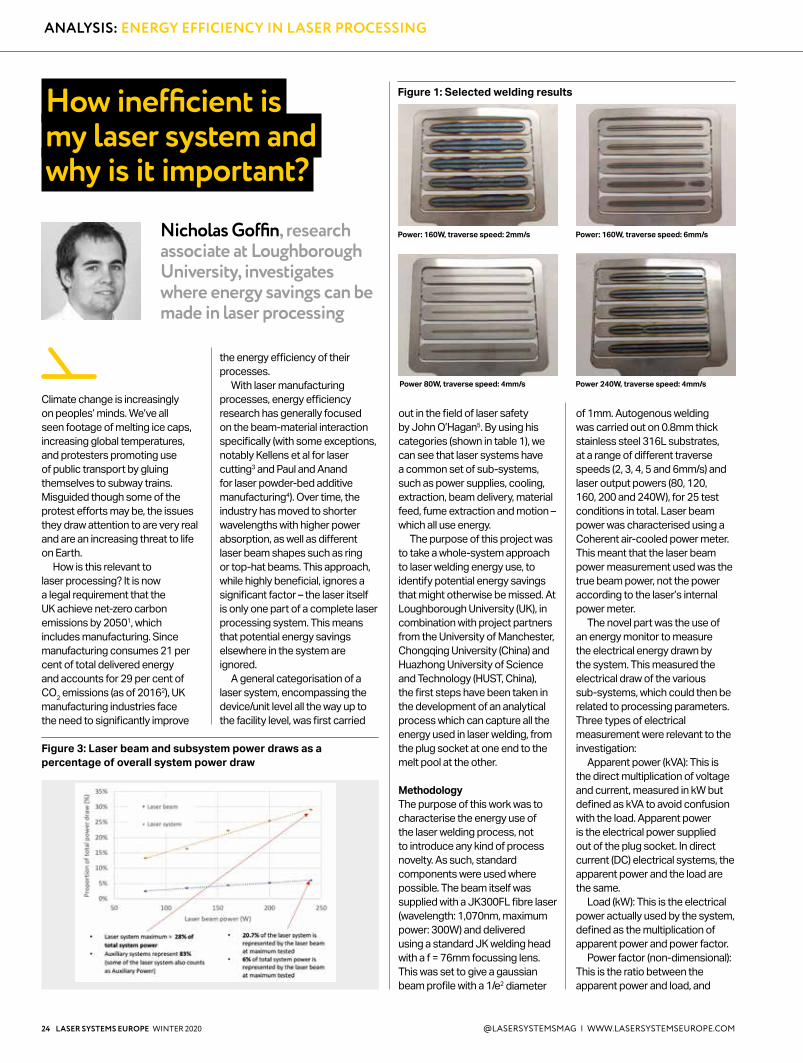
Nicholas Goffin, research associate at Loughborough University, investigates where energy savings can be made in laser processing
@researchinfo | www.researchinformation.info
Climate change is increasingly on peoples’ minds. We’ve all seen footage of melting ice caps, increasing global temperatures, and protesters promoting use of public transport by gluing themselves to subway trains. Misguided though some of the protest efforts may be, the issues they draw attention to are very real and are an increasing threat to life on Earth.
How is this relevant to laser processing? It is now a legal requirement that the UK achieve net-zero carbon emissions by 20501, which includes manufacturing. Since manufacturing consumes 21 per cent of total delivered energy and accounts for 29 per cent of CO2 emissions (as of 20162), UK manufacturing industries face the need to significantly improve
the energy efficiency of their processes.
With laser manufacturing processes, energy efficiency research has generally focused on the beam-material interaction specifically (with some exceptions, notably Kellens et al for laser cutting3 and Paul and Anand for laser powder-bed additive manufacturing4). Over time, the industry has moved to shorter wavelengths with higher power absorption, as well as different laser beam shapes such as ring or top-hat beams. This approach, while highly beneficial, ignores a significant factor – the laser itself is only one part of a complete laser processing system. This means that potential energy savings elsewhere in the system are ignored.
A general categorisation of a laser system, encompassing the device/unit level all the way up to the facility level, was first carried
out in the field of laser safety by John O’Hagan5. By using his categories (shown in table 1), we can see that laser systems have a common set of sub-systems, such as power supplies, cooling, extraction, beam delivery, material feed, fume extraction and motion – which all use energy.
The purpose of this project was to take a whole-system approach to laser welding energy use, to identify potential energy savings that might otherwise be missed. At Loughborough University (UK), in combination with project partners from the University of Manchester, Chongqing University (China) and Huazhong University of Science and Technology (HUST, China), the first steps have been taken in the development of an analytical process which can capture all the energy used in laser welding, from the plug socket at one end to the melt pool at the other.
MethodologyThe purpose of this work was to characterise the energy use of the laser welding process, not to introduce any kind of process novelty. As such, standard components were used where possible. The beam itself was supplied with a JK300FL fibre laser (wavelength: 1,070nm, maximum power: 300W) and delivered using a standard JK welding head with a f = 76mm focussing lens. This was set to give a gaussian beam profile with a 1/e2 diameter
How inefficient is my laser system and why is it important?
24 LASER SYSTEMS EUROPE WINTER 2020 @LASERSYSTEMSMAG | WWW.LASERSYSTEMSEUROPE.COM
ANALYSIS: ENERGY EFFICIENCY IN LASER PROCESSING
Figure 1: Selected welding results
Figure 3: Laser beam and subsystem power draws as a percentage of overall system power draw
of 1mm. Autogenous welding was carried out on 0.8mm thick stainless steel 316L substrates, at a range of different traverse speeds (2, 3, 4, 5 and 6mm/s) and laser output powers (80, 120, 160, 200 and 240W), for 25 test conditions in total. Laser beam power was characterised using a Coherent air-cooled power meter. This meant that the laser beam power measurement used was the true beam power, not the power according to the laser’s internal power meter.
The novel part was the use of an energy monitor to measure the electrical energy drawn by the system. This measured the electrical draw of the various sub-systems, which could then be related to processing parameters. Three types of electrical measurement were relevant to the investigation:
Apparent power (kVA): This is the direct multiplication of voltage and current, measured in kW but defined as kVA to avoid confusion with the load. Apparent power is the electrical power supplied out of the plug socket. In direct current (DC) electrical systems, the apparent power and the load are the same.
Load (kW): This is the electrical power actually used by the system, defined as the multiplication of apparent power and power factor.
Power factor (non-dimensional): This is the ratio between the apparent power and load, and
Power: 160W, traverse speed: 2mm/s Power: 160W, traverse speed: 6mm/s
Power 240W, traverse speed: 4mm/s Power 80W, traverse speed: 4mm/s

WINTER 2020 LASER SYSTEMS EUROPE 25
is analogous to efficiency in mechanical systems.
The power draws of the various sub-systems were then characterised according to their role in the welding process. This categorisation happened in a similar way to the Embodied Product Energy (EPE) model created by Seow et al6. Modified laser-specific versions of those categories were defined as follows:
Processing power (PP): A laser-specific modification of the concept of direct energy (DE), which is the sum of all of the power inputs that directly contribute to the melting process. For this investigation, this was only the laser beam, but it is easy to imagine a scenario with a hybrid laser-arc torch or preheating,
WWW.LASERSYSTEMSEUROPE.COM | @LASERSYSTEMSMAG
ANALYSIS: ENERGY EFFICIENCY IN LASER PROCESSING
which would also be included. Saving energy in this area is where the majority of laser welding research has tended to focus its efforts.
Auxiliary power (AP): This is the sum of all the process inputs that make it function, but do not directly contribute to the melting itself. This covers subsystems such as cooling, extraction and motion.
Electrical supply waste (ESW): This category incorporates the sum of all the electrical losses, as calculated from the apparent power and the power factor. Short of complete redesign of subsystem equipment, there are no energy savings available here.
For the purposes of this investigation, five subsystems were defined – laser, cooling,
extraction, motion, and support systems (computer, lights, interlocks etc).
ResultsAs desired, welding results showed an utterly predictable process with nothing unexpected occurring that could trouble the energy readings. Examples from these results are shown in figure 1.
When traverse speed is increased at constant power (160W), the specific energy decreases from 80J/mm to 26.7J/mm, thus the weld track gets smaller. When power increases at a given traverse speed (4mm/s) specific energy increases from 20J/mm to 60J/mm, thus the weld track gets larger.
When the energy was measured for all the laser subsystems, it was found that the laser subsystem represented a minority portion of the total power drawn by the welding system. Figure 2 shows these energy flows in the form of Sankey diagrams at different laser beam power levels. ESW occupied a significant proportion of the electrical power draw as well, but the vast majority of power draw was actually taken by auxiliary systems (auxiliary power), not by the laser itself.
It was also found that laser processing parameters affect overall system power draw, as illustrated in figure 3. As the laser power increases, its electrical power draw also increases. Other subsystems, such as the extraction, stay constant, with the result that the laser subsystem takes up an increasing proportion
of total power as the laser beam power increases.
ConclusionIn this investigation, the various types of energy used by the laser welding system have been categorised and quantified, so as to assist decision-making for energy saving. We have shown that the laser beam and subsystem itself actually represent a minority portion of the total electricity used by a laser welding system.
To maximise energy saving, it would therefore be wise for operators and system designers to look beyond the laser, at the wider system – for example, in the cooling, extraction and motion subsystems – because energy savings made in those areas can potentially eclipse those achieved via the laser itself. The proportion of total power taken by the laser also changes depending on parameters, which means that energy saving measures will have varying levels of effectiveness, depending on what parameters the particular system is using. l
References[1] UK Department for Business Energy and
Industrial Strategy, The Climate Change Act 2008 (2050 Target Amendment) Order 2019. SI 2019/1056.
[2] PW Griffin, GP Hammond and JB Norman, ‘Indus-trial energy use and carbon emissions reduction: a UK perspective,’ Wiley Interdiscip. Rev. Energy Environ., vol. 5, no. 6, pp. 684–714, Nov. 2016.
[3] K Kellens, GC Rodrigues, W Dewulf and JR Duflou, ‘Energy and resource efficiency of laser cutting processes,’ Phys. Procedia, vol. 56, no. C, pp. 854–864, 2014.
[4] R Paul and S Anand, ‘Process energy analysis and optimization in selective laser sintering,’ J. Manuf. Syst., vol. 31, no. 4, pp. 429–437, 2012.
[5] JB O’Hagan, ‘Safety Aspects of Laser Displays,’ Radiat. Prot. Dosimetry, vol. 72, no. 3, pp. 241–248, Aug. 1997.
[6] Y Seow and S Rahimifard, ‘A framework for mod-elling energy consumption within manufacturing systems,’ CIRP J. Manuf. Sci. Technol., vol 4, no 3, pp 258-264, 2011.
Figure 2: Laser welding energy flows at different beam power levels
Category Energy/Resource consuming sub-system
Laser Power supplyCooling systemLaser consumables (such as gas)Computers and control systems
Beam Delivery Powered beam deflection systemsOptical componentsBeam inspection
Process Motion systemsSafety systemsFume extractionPower measurementComputers and control systemsMaterial feed/deliveryMaterial processes (such as preheating)
People and Environment
HeatingLighting
Table 1: Common laser subsystems
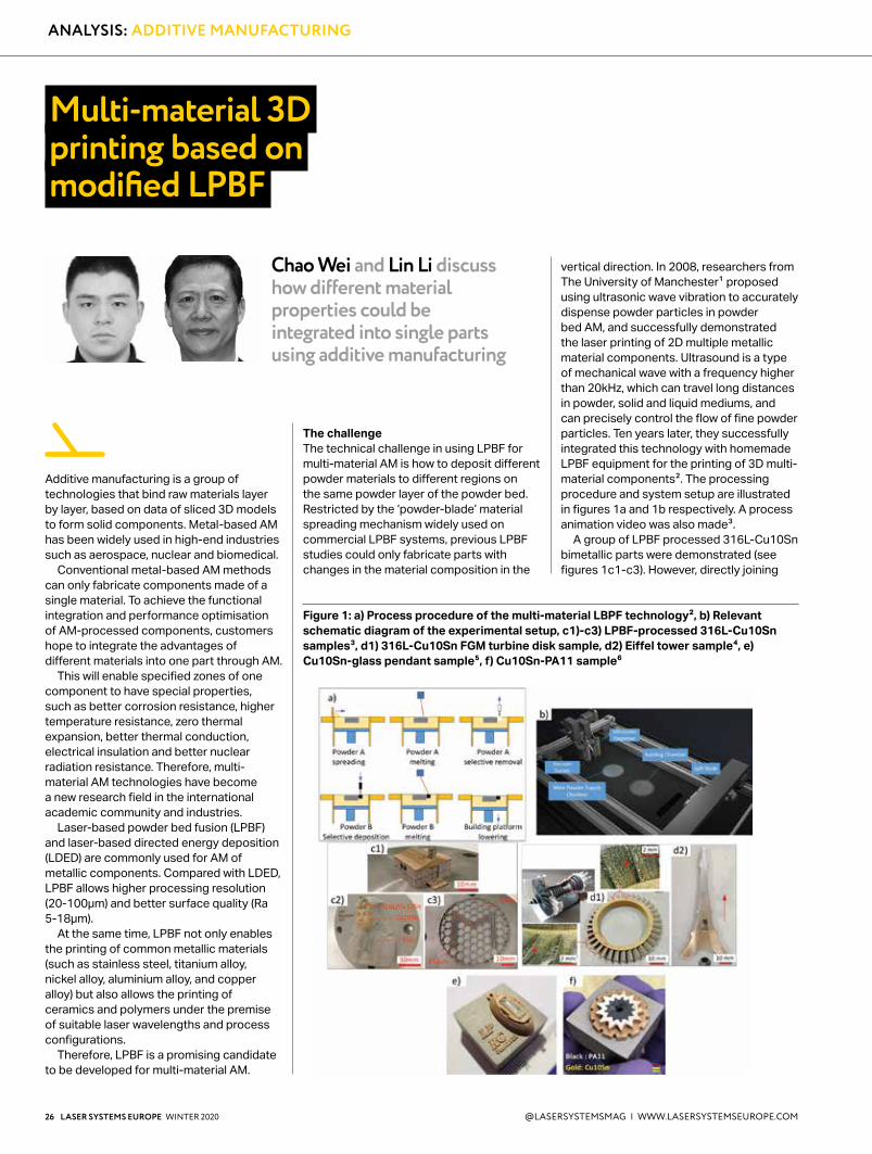
Chao Wei and Lin Li discuss how different material properties could be integrated into single parts using additive manufacturing
@researchinfo | www.researchinformation.info
Additive manufacturing is a group of technologies that bind raw materials layer by layer, based on data of sliced 3D models to form solid components. Metal-based AM has been widely used in high-end industries such as aerospace, nuclear and biomedical.
Conventional metal-based AM methods can only fabricate components made of a single material. To achieve the functional integration and performance optimisation of AM-processed components, customers hope to integrate the advantages of different materials into one part through AM.
This will enable specified zones of one component to have special properties, such as better corrosion resistance, higher temperature resistance, zero thermal expansion, better thermal conduction, electrical insulation and better nuclear radiation resistance. Therefore, multi-material AM technologies have become a new research field in the international academic community and industries.
Laser-based powder bed fusion (LPBF) and laser-based directed energy deposition (LDED) are commonly used for AM of metallic components. Compared with LDED, LPBF allows higher processing resolution (20-100μm) and better surface quality (Ra 5-18μm).
At the same time, LPBF not only enables the printing of common metallic materials (such as stainless steel, titanium alloy, nickel alloy, aluminium alloy, and copper alloy) but also allows the printing of ceramics and polymers under the premise of suitable laser wavelengths and process configurations.
Therefore, LPBF is a promising candidate to be developed for multi-material AM.
The challengeThe technical challenge in using LPBF for multi-material AM is how to deposit different powder materials to different regions on the same powder layer of the powder bed. Restricted by the ‘powder-blade’ material spreading mechanism widely used on commercial LPBF systems, previous LPBF studies could only fabricate parts with changes in the material composition in the
Multi-material 3Dprinting based onmodified LPBF
26 LASER SYSTEMS EUROPE WINTER 2020 @LASERSYSTEMSMAG | WWW.LASERSYSTEMSEUROPE.COM
ANALYSIS: ADDITIVE MANUFACTURING
Figure 1: a) Process procedure of the multi-material LBPF technology2, b) Relevant schematic diagram of the experimental setup, c1)-c3) LPBF-processed 316L-Cu10Sn samples3, d1) 316L-Cu10Sn FGM turbine disk sample, d2) Eiffel tower sample4, e) Cu10Sn-glass pendant sample5, f) Cu10Sn-PA11 sample6
vertical direction. In 2008, researchers from The University of Manchester1 proposed using ultrasonic wave vibration to accurately dispense powder particles in powder bed AM, and successfully demonstrated the laser printing of 2D multiple metallic material components. Ultrasound is a type of mechanical wave with a frequency higher than 20kHz, which can travel long distances in powder, solid and liquid mediums, and can precisely control the flow of fine powder particles. Ten years later, they successfully integrated this technology with homemade LPBF equipment for the printing of 3D multi-material components2. The processing procedure and system setup are illustrated in figures 1a and 1b respectively. A process animation video was also made3.
A group of LPBF processed 316L-Cu10Sn bimetallic parts were demonstrated (see figures 1c1-c3). However, directly joining

WINTER 2020 LASER SYSTEMS EUROPE 27
two dissimilar materials often leads to defects, such as cracks and pores at the material interface, which may lead to the fracture of components in service. To address this, they added a functionally graded material (FGM) transition layer at the interface of the two materials, to make the material composition transition from A to B smoothly. Demonstration samples are presented in figures 1d1-d3. In addition to metal-based multi-material combinations, they also further used this technology to process metal-glass, metal-ceramic and
WWW.LASERSYSTEMSEUROPE.COM | @LASERSYSTEMSMAG
ANALYSIS: ADDITIVE MANUFACTURING
metal-polymer combinations, as shown in figures 1e and 1f.
Researchers from The University of Manchester7 demonstrated how this technology can be used for embedding anti-counterfeiting features inside AM-processed 316L components. A QR code of high-density copper alloy, as shown in Figure 2 a, can be used. The density of copper alloy is higher than stainless steel, so the QR code can be easily identified by x-ray inspection and thermal imaging, as in figure 2 b and c respectively. In addition, they also demonstrated easy-to-remove support structures made of a metal-ceramic mixture composed of silicon carbide (SiC) and stainless-steel powder in the LPBF processed 316L component8. The high melting point SiC cannot be easily melted by a laser, which increases the porosity of the support structure and deteriorates its strength, so it is easier to remove.
Application areas and further challengesThis technology has many potential applications including the production
of aerospace components (bimetallic temperature sensors, zero thermal expansion parts), nuclear components (plasma-facing components, heat exchangers), electronic products (multi-material circuit boards, embedded sensors, micro-electromechanical systems), and biomedical components (biocompatible implants).
Although it is feasible to integrate multiple materials into the same part through LPBF, this method still faces challenges from the viewpoint of materials science. Significant differences in the physical properties of dissimilar materials can easily lead to defects in the microstructure of AM-processed materials, such as pores, cracks, brittle intermetallic compounds, and lack of fusion. The University of Manchester is co-operating with industrial partners, including those from the nuclear industry, to carry out in-depth materials research, and it is hoped that the real application of this technology in the industry can be seen in the near future. l
“Multi-material AM technologies have become a new research field in the international academic community and industries”
Dr Chao Wei is a postdoctoral research associate and Professor Lin Li is the director of the Laser Processing Research Centre, at The University of Manchester
Figure 2: a) A copper QR code embedded in AM processed stainless-steel components, b) x-ray image, c) IR image of the sample with an embedded QR code⁷
References: [1] OM Al-Jamal, S Hinduja, L Li, Characteristics
of the bond in Cu-H13 tool steel parts fabricated using SLM, CIRP Ann. - Manuf. Technol. 57 (2008) 239–242. doi:10.1016/j.cirp.2008.03.010.
[2] C Wei, L Li, X Zhang, YH Chueh, 3D printing ofmultiple metallic materials via modified selective laser melting, CIRP Ann. 67 (2018) 245–248. doi:10.1016/j.cirp.2018.04.096.
[3] https://www.youtube.com/watch?v=TtY5nPqMvqU
[4] C Wei, Z Sun, Q Chen, Z Liu, L Li, Additive manufacturing of horizontal and 3D functionally graded 316L/Cu10Sn components via multiple material selective laser melting, J. Manuf. Sci. Eng. 141 (2019) 1–14. http://dx.doi.org/10.1115/1.4043983.
[5] X Zhang, C Wei, YH Chueh, L Li, An integrated dual ultrasonic selective powder dispensing platform for three-dimensional printing of multiple material metal/glass objects in selective laser melting, J. Manuf. Sci. Eng. Trans. ASME. 141 (2019) 1–12. doi:10.1115/1.4041427.
[6] Y Chueh, X Zhang, JC-R Ke, Q Li, C Wei, L Li, Additive manufacturing of hybrid metal/polymer objects via multiple-material laser powder bed fusion, Addit. Manuf. 101465 (2020).
[7] C Wei, Z Sun, Y Huang, L Li, Embedding Anti-counterfeiting Features in Metallic Components via Multiple Material Additive Manufacturing, Addit. Manuf. 24 (2018) 1–12. doi:10.1016/j.addma.2018.09.003.
[8] C Wei, Y-H Chueh, X Zhang, Y Huang, Q. Chen, L Li, Easy-To-Remove composite support material and procedure in additive manufacturing of metallic components using multiple material laser-based powder bed fusion, J. Manuf. Sci. Eng. 141 (2019) 1–18. http://dx.doi.org/10.1115/1.4043536.

NEWS FROM AILU
Dave MacLellan, executive director of AILU, describes the new features of ILAS 2021
Those who have attended AILU networking events (workshops, ILAS or LPM 2018) will know that networking, social interaction and good food are some of the essential success factors of laser community events. Next year in March, due to the pandemic, the rescheduled 7th ILAS (Industrial Laser Applications Symposium) will take place as an online event. While there will be no food provided, there will be plenty of opportunity to network and meet face-to-face with new connections and familiar faces.
Fantastic exhibition experienceSome online events are very passive, with no interactivity. In contrast to this, ILAS will have a live exhibition with staff attending during the planned exhibition hours – morning break, lunch and afternoon break on both days.
Outside of exhibition hours, delegates can explore the meeting hub and search for people they know, or who they want to meet. After a connection request is accepted, contact information is shared and a video or text chat can be started straight away, or scheduled for later on.
Exhibitors can provide as many staff during the core hours as they wish (two people are included in the exhibitor package). Visitors can see who is online and request a chat, join a queue or talk to the next available person on the stand. There is no limit to the
content exhibitors can upload as documents, video links or website landing pages.
Opportunities for student presentersResearchers who have been unable to present their findings in the past year have a great opportunity as poster presenters at ILAS. Poster presenters can upload their poster in a format for download by delegates. They can also upload a short video describing their poster, and during the early evening poster
session, they can present it live to a small audience or individuals depending on their choice and the demand at the session.
Catch-up TVWith three parallel sessions, there is always the chance you might miss a presentation you really want to see because it clashes with another of your interests. At ILAS 2021, any presentation you have missed (or want to watch again) will be available for 12 months to all registered delegates on Vimeo. This allows delegates to plan the two days of ILAS according to priorities for visiting exhibitors, listening live to presentations, checking posters, attending plenary sessions and meeting with peers using Meeting Hub.
Talent requiredAs part of the evening entertainment there will be a live awards ceremony followed by live entertainment on Zoom. Musicians are invited to send us their audition recordings if they would like to perform at ILAS 2021 – if you are skilled at singing or playing an instrument, we would love to hear you.
Depending on demand there will be the opportunity for 5 to 10 minutes of performance in the programme for the evening. The evening time will suit all European time zones and also the USA.
Better value than everWith no time wasted in travel, no flights or hotels to pay for and lower registration fees, ILAS is more accessible than ever. Prices are 40 to 50 per cent lower on average than past ILAS events (as food and drink is not provided), and the event will attract a large European audience. It will be accessible to universities and research centres, who will be able to send a large number of researchers to experience a world-class
Meeting face-to-face at ILAS 2021 – some online advantages
laser technology event, present their research and catch up with the state-of-the-art in industrial products and research into applications, optics and automation.
Register nowDon’t leave it too late to register for ILAS 2021, on 24 and 25 March. You can register and pay online, or contact the AILU office for invoicing options. AILU now accepts online payment for credit and debit cards. As there is no travel or accommodation, the event is expected to be very popular and the event site will be live one week before ILAS for familiarisation. Exhibitors and presenters will have pre-event training and instructions to allow them to make the most of their ILAS experience.
We look forward to seeing you in March! l
“Visitors can request a chat, join a queue or talk to the next available person on the exhibitor stand”
www.ailu.org.uk/eventswww.ilas2021.co.uk [email protected] • +44 1235 539595
ILAS 20217th Industrial Laser Applications Symposium
Delegates will be able to choose who to meet at the Exhibition
Poster presenters can present live to delegates in groups or individually
28 LASER SYSTEMS EUROPE WINTER 2020 @LASERSYSTEMSMAG | WWW.LASERSYSTEMSEUROPE.COM

PRODUCT UPDATE
WINTER 2020 LASER SYSTEMS EUROPE 29WWW.LASERSYSTEMSEUROPE.COM | @LASERSYSTEMSMAG
LASER SYSTEMS
MicroVega xMR3D-Micromac has introduced a selective laser annealing system for magnetic sensor formation: the MicroVega xMR.
Incorporating a highly flexible, high-throughput tool configuration, the new system accommodates both giant magnetoresistance and tunnel magnetoresistance sensors, and easily adjusts magnetic orientation, sensor position and sensor dimension.
The MicroVega xMR provides several advantages over thermal annealing for magnetic sensor manufacturing. These include higher precision to enable the processing of smaller magnetic device structures, which results in more devices per wafer, as well as the ability to set different reference magnetisation directions on sensors across a single wafer.
The system’s on-the-fly spot and variable laser energy provide selective heating of the pinning layer in each sensor to ‘imprint’ the intended magnetic orientation. Magnetic field strength and orientation is adjustable
by recipe, while high-temperature gradients ensure low thermal impact. This allows sensors to be processed directly next to read-out electronics, as well as closer together, and enables the production of smaller sensors – freeing up space for processing more devices per wafer. The result is reduced process steps, simplified production flow, higher yield and more cost-effective production of integrated monolithic sensor packages.http://3d-micromac.com
LightWeldIPG Photonics has launched LightWeld, a handheld laser welding system offering extremely small size and weight, as well as air-cooling.
The system offers 1.5kW laser power, which can be easily adjusted. Select stored modes provide up to 2.5kW of high peak power for even greater welding capability.
LightWeld comes with wobble welding that provides 5mm of additional weld width, increasing capability, while providing aesthetic seams. Other standard features include: a 5m delivery cable for increased part access; connections for gas and external connectivity; multi-level sensors and interlocks for operator safety; and a laser-welding gun with wobble/scan capabilities that supports wire feeder and welding tip configurations.
Simple controls, including 74 stored preset and user-defined process parameters, allow novice welders to be trained and welding in a few hours. The rapid and flexible processing capabilities of LightWeld enable it to join thick, thin and reflective metals with minimal distortion, deformation, undercut or burn-through.
Compared with traditional MIG and TIG welders, it enables much faster welding, is easier to learn and operate, and provides consistent, high-quality results across a range of materials and thicknesses, with low heat input and aesthetic finishes, with minimal or no filler wire.www.ipgphotonics.com
PRODUCTUPDATE
15kW ByStar FiberBystronic has upped the power of its ByStar Fiber 3015 and 4020 systems to 15kW.
The new 15kW laser source increases cutting speeds by 50 per cent compared to a 10kW source. This means that sheet metal processing companies can now benefit from higher productivity at low unit costs. The new systems cut steel, aluminium, and stainless steel precisely and reliably in thicknesses between 1 to 30mm, and brass and copper in thicknesses of 20mm.
The 15kW laser output now enables extended applications in steel and aluminium
of up to 50mm, therefore offering maximum flexibility both for large series and urgent customer orders. Regardless of whether cutting aluminium, non-ferrous metals, or steel, the high-performance Bystronic cutting head offers exceptional precision in both thin and thick sheets and profiles.www.bystronic.co.uk
OPTICS
Silverline F-theta lens for USP laser processingWith the new F-theta lens for 532nm applications, Jenoptik has released another lens for the high-volume laser production of printed circuit boards (PCBs).
This is the second high-power lens for use in the green wavelength range in Jenoptik’s
Silverline lens portfolio. The solid-fused silica lens is especially designed for high-volume electronic production with ultrashort pulse lasers such as PCB depaneling.
Enabled by its low-absorption fused silica and high-quality coating, it withstands ultrashort pulse lasers and lasers with
power outputs up to the kilowatt range. With a 163mm focal length and 13μm minimum spot size, workpieces can be processed in a scan field of 65 x 65mm. The optimised lens design and innovative lens mounting allow the lens’ full performance to be used, with no back reflections.www.jenoptik.com

LASER SYSTEMS
Linos Telecentric F-Theta-Ronar 250mm lensExcelitas Technologies has released the Linos Telecentric F-Theta-Ronar 250mm lens for 515 to 540nm.
A standard F-Theta lens that includes FEM simulation, the new 250mm features an interchangeable, coated protective glass made of fused silica and advanced mounting technologies for a large telecentric scan field.
Ideal for use in applications such as PCB drilling and non-ferrous metal processing welding, cutting and additive manufacturing, F-Theta-Ronar 250mm lenses offer high-power suitability, combined with the following advantages:
• Large effective focal length, enabling a very large working distance position
• Telecentric design of <0.5°• Fused-silica design with an
entrance aperture of 14mm• FEM simulation• Interchangeable, coated
protective glass made of fused silica
• Standard M85x1 connecting thread
www.excelitas.com
AFX-1000NLight has introduced the AFX-1000 for metal additive manufacturing. Leveraging programmable laser technology, the AFX-1000 is a high-power fibre laser that can switch between a single-mode beam and other beam profiles without free space optics.
The AFX ring mode geometry stabilises large melt pools, reducing soot and spatter to improve material quality and production yields. Discrete AFX beam profiles can be selected on-the-fly at 30 times per second, offering more freedom to control melting and solidification rates, physical microstructure and thermal strain that can lead to stress fractures – a frequent cause of part failure. Ring mode processing with a single AFX
laser has been shown to produce ‘fully dense’ material (>99.5 per cent) at build rates exceeding 100cm3/hr with a single laser.www.nlight.net
Jasper FlexFluence has introduced a 30W femtosecond laser, Jasper Flex, intended for systems with volume constraints that require high laser power and exceptional pulse quality.
The Jasper Flex is a smaller version of the firm’s Jasper laser, an all-fibre high-power laser built using SESAM-free technology. Both models provide exceptional reliability and an excellent lifespan for users.
The Jasper Flex’s all-fibre, SESAM-free oscillator has been tested to operate at 40g vibration and in a vast range of temperatures (spanning more than 50°C). The oscillator, together with a fibre preamplifier, creates a monolithic construction immune to misalignment.
Jasper Flex, together with optional
harmonic modules (SHG, THG, FHG), is a versatile tool especially useful in applications such as display repairs and micromachining. It offers broad pulse duration option tuning from <250fs up to 20ps. In addition, Jasper Flex comes with a burst option included as standard, which delivers a nanosecond long burst of individual femtosecond pulses.https://fluence.technology
SR AOMLuxinar has launched the SR AOM range of sealed CO2 lasers for high-precision applications that require a reduced heat affected zone.
The new SR 10 AOM and SR 25 AOM are both available at a wavelength of 9.3µm and with rated powers of 75 and 150W respectively. The integrated acousto-optic modulator (AOM) creates much faster optical rise and fall times of less than 1µs, which can minimise unnecessary heat energy from typical pulse rise/fall times of approximately 60µs.
The AOM range provides exceptional pulse-to-pulse control, output power stability and an integrated and field replaceable RF power supply for ease of installation and servicing at customer sites. The simple control interface and compact mechanical design of the unit allow easy integration into a variety of laser-based processing machines.
The RF power supply, AOM, control driver and optical parts of the SR 10 AOM and SR 25 AOM are all hermetically-sealed to IP66.www.luxinar.com
OPTICS
Large angle line shapersHolo/Or has announced new large angle line shapers, responding to increasing demand for line shaping solutions with wide angles to enable high throughput processing of a large area in laser annealing or ablation applications.
Using a line-shaped uniform laser beam has clear throughput advantages over step and repeat methods when treating large areas. Using the large line shaper in a single mode laser system achieves high-peak intensity over a large area by shaping the beam to a
narrow, diffraction-limited line.The large line shaper offers
line angles greater than 150mRad, while maintaining diffraction-limited line width.
The line exhibits a flat-top uniform intensity profile over the entire length, with sharp diffraction-limited drops at the edges. This diffractive element is suitable for high
damage threshold applications, and can be optimised from DUV to NIR wavelengths.
The new large angle line shapers are available via Laser Components.www.holoor.co.il
30 LASER SYSTEMS EUROPE WINTER 2020 @LASERSYSTEMSMAG | WWW.LASERSYSTEMSEUROPE.COM
PRODUCT UPDATE

LIA NEWS
g
WINTER 2020 LASER SYSTEMS EUROPE 31WWW.LASERSYSTEMSEUROPE.COM | @LASERSYSTEMSMAG
NEWS FROM LIA
ICALEO 2020 – a virtual experienceJana Langhans, of LIA, recaps this year’s ICALEO conference, held online for the first time in October
The International Congress on Applications of Lasers and Electro-Optics (ICALEO), hosted annually by the Laser Institute of America (LIA), ended in 2019 with so many faces saying ‘see you next year in Chicago!’ We were all looking forward to meeting up with old and new friends this year, kicking off the conference by catching up over food at the welcome reception. No one could have predicted what ICALEO 2020 would actually look like. In the wake of the Covid-19 pandemic, there were unfortunately a lot of events in our industry, like all others, that were forced to cancel. With the pandemic hitting the United States early in 2020, some conferences that were meant to be held later in the year were able to take some time to convert their events to be virtual. ICALEO was lucky enough to be one of those, which is how we got to ICALEO 2020 – a virtual experience.
Traditionally an in-person four-day event packed with presentations in different industry-specific tracks, ICALEO had to be transformed to accommodate an audience virtually. That unfortunately meant cutting down content to fit into two days; still packed with those same interesting presentations, but now virtually. The five tracks this year were laser additive manufacturing, laser macroprocessing, laser microprocessing, laser nanomanufacturing, and frontiers in laser applications.
Each had themed sessions that ran concurrently throughout both days. There were 129 total presentations throughout the five tracks and 41 accepted peer-reviewed manuscripts. These peer-reviewed works will be published in the Journal of Laser Applications.
Some of the most anticipated talks were, of course, the opening and closing plenaries. Infographic showing ICALEO 2020 registrations by region
The conference began after a few opening remarks with Dr Ty Olmstead’s talk on the successes of biophotonics and what new opportunities are arising in the future.
Next, Dr Abdalla Nassar gave his presentation on quality assurance in laser-based, metal additive manufacturing. The last speaker of the opening plenary was Professor Kenichi Ishikawa, who discussed building science and theory for smart laser manufacturing. For the closing plenaries to wrap up the conference, Professor Jyoti Mazumder gave a presentation discussing the past, present, and future of metal additive manufacturing. Finally, Dr Nina Lanza shared
her work in space exploration, including how laser-based analysis techniques can be used on Mars.
Two of these plenary speakers could also be seen in one of the special highlights of ICALEO 2020, the live panel session ‘Lasers in the photonics era: from manufacturing factory to space exploration’. Moderated by the esteemed Dr William Steen, he led a very engaging discussion with special guests Dr Aravinda Kar, Dr Islam Salama, Dr Olmstead, and Dr Lanza. Each panellist is an industry expert in different fields, bringing their own special knowledge and perspective to the given topics and audience questions.
They began with a discussion about how working with lasers has evolved over the past few decades. Each one discussed how they have seen it develop most in their personal areas of expertise, including laser processing, manufacturing and space exploration. They also had a very interesting discussion about how artificial intelligence is up-and-coming, and how it has played a role in the various aspects of the laser industry.
“Some speakers called in at midnight their time to be available for questions, which says a lot about the community of ICALEO”

Something that was important when picking from the many different options in how to format a virtual conference, was picking one that best fit a traditional ICALEO feel. In a typical live event, attendees are in the same room as the speaker, and can interact with them and ask questions about their presentation. So each presentation had the opportunity for attendees watching live to engage in a short question and answer session with the speaker, by submitting their questions into the virtual platform. These questions would then be relayed to the speakers to answer live from wherever they were. This required a lot of co-ordination from the back end between LIA staff, virtual platform technicians, session chairs, and presenters, but it was a unique experience, and everyone worked well together, which made things run pretty smoothly.
Since ICALEO is an international conference with speakers and attendees from many different countries around the world, this was a unique opportunity for them to still be involved despite travel restrictions.
Unfortunately, due to speakers being from different time zones, not all of them were able to attend live, but the majority were still able to participate. We even had some speakers call in at midnight their time to be available for questions, which says a lot about the community of ICALEO that participants are so committed to sharing their contribution with the industry.
A feature of the virtual format we were particularly excited to share is the On-Demand Library. Cognizant of the fact that many ICALEO attendees are international, and therefore in various time zones, the idea behind having an on-demand library was so anyone could register, then watch presentations in their own time.
While there were unique benefits to participating in the live portion of the conference, all presentations from the conference, as well as a few extra presentations, were recorded and are now available to watch at any point for the entire
g
LIA NEWS
About LIALIA is The Institute for Photonic Materials Processing Innovation. Our vision is to help make the world a better place through safe, optimal and novel use of lasers, optics and photonics, including quantum science and technology, and their application to advanced materials.
www.lia.org
13501 Ingenuity Drive, Ste 128, Orlando, FL 32826, +1 407.380.1553
year. This was also a benefit to attendees of the live event, who had interests in multiple tracks, because they didn’t have to choose between concurrent presentations to attend, if there were multiple talks they wanted to see.
One of the biggest challenges of adapting to a completely new format is having a short time to learn an entirely new platform, and how to organise content in a new way. It was also challenging to make the conference engaging enough to work against the ‘virtual event fatigue’ that many people seem to be experiencing, due to having only been able to attend virtual versions of everything they are used to this year: conferences, meetings, webinars, etc. Despite these challenges,
ICALEO 2020 had the highest number of registrants in the conference’s 39-year history.
In total, 854 people registered for the 2020 virtual conference and on-demand library. Attendees and participants joined us from 44 different countries around the world. We can, of course, thank our registration sponsor and the convenience of a virtual conference for these record numbers, but we should also credit this year’s ICALEO volunteers, members, and staff on their dedication to continue to provide quality presentations, as well as their commitment to being inclusive of international participants and attendees.
We know that a virtual conference could never quite replace an in-person event, but overall, the responses to ICALEO 2020 have been positive. In a survey sent out to attendees shortly after the conference, 75 per cent of responses rated the conference
itself as excellent or above average, and the overall quality of content was rated as 74 per cent excellent or above average. We also surveyed our speakers to get an idea of how they felt their experience went. The overall presenter experience had 94 per cent of speakers rate good or great and overall satisfaction with management of the conference process had 88 per cent rate satisfied or very satisfied.
The main feedback we received was that although the virtual conference was convenient and the talks were informative, attendees missed the networking of a live event, which is understandable.
The results from both surveys also showed us that the majority of people would participate/attend virtually again if it comes to that in 2021.
As any organisation that hosted a virtual event in place of a physical event this year is sure to know, adjusting to the new format is definitely a learning experience. The pandemic has required a change in the way pretty much everything is done. Having conferences change to virtual experiences is something that we believe will have a major influence on the future and will never fully go away. Even as travel and larger gatherings start coming back, the virtual aspect will likely still play a role in most events.
This can be said of LIA’s own events as we look ahead to next year and the years beyond. We have two conferences coming up in 2021: International Laser Safety Conference (ILSC) and our next ICALEO.
We are still hoping to have them both as live, in-person events. However, we also know that not everyone will be comfortable or even able to travel in the upcoming months, so we are looking at virtual options to accompany the physical format, to reach as many people as possible. Whatever happens, we look forward to continuing to connect with our community, and doing our part in sharing industry research and developments.
If you were not able to participate in or attend our virtual ICALEO 2020 conference, and would like access to the recordings in the on-demand library, please contact [email protected] for more information. l
32 LASER SYSTEMS EUROPE WINTER 2020 @LASERSYSTEMSMAG | WWW.LASERSYSTEMSEUROPE.COM
“The panellists discussed how AI is up-and-coming and how it plays a role in various aspects of the laser industry”
The virtual panel discussion ‘Lasers in the photonics era: from manufacturing factory to space exploration’

2022Rosen Centre
HotelOrlando, FL
October 17th - 20th
2023Palmer House
Hilton Chicago, IL
October 16th - 19th
Contact [email protected] for more informationwww.icaleo.org
Presented by:
October 18-21
2021San Diego, California
Sheraton San Diego Hotel
and Marina

@researchinfo | www.researchinformation.info34 LASER SYSTEMS EUROPE WINTER 2020 @LASERSYSTEMSMAG | WWW.LASERSYSTEMSEUROPE.COM
SUPPLIERS DIRECTORY
SUPPLIERSDIRECTORY
El.En. S.p.A.Via Baldanzese, 1750041 Calenzano - Firenze - ItalyTel. +39 055 8826807 l Fax +39 055 8832884https://elenlaser.com
Producing innovation since 1981El.En. is an italian laser company based in Florence. We produce CO2 laser sources, laser scanning heads and custom laser devices for the manufacturing industry. With El.En. you can count on reliability, durability and expert technical assistance because all the core components of our devices are engineered and produced in-house. Our laser sources are geared to achieve speed, precision and ease of integration in a wide range of applications. This is why since 1981 we’ve been working with more than 2000 companies worldwide, gaining a considerable experience in a wide range of markets. Start making with El.En!
Industrial Laser Division
Aerotech United KingdomThe Old Brick Kiln, Ramsdell, Tadley, Hampshire RG26 5PRTel: +44 (0)1256 855055 Fax: +44 (0)1256 855649 [email protected] l www.aerotech.co.uk
Aerotech serves the unique requirements of laser processing and laser machining applications by manufacturing high performance systems and components for laser applications.Aerotech developments in the areas of mechanics, controls, software and laser control have provided end users, systems integrators and OEMs with the best possible laser cutting, welding, etching, and marking systems available.
ADVERTISE HERE AND ONLINE For details please contact Jon Hunt on +44(0)1223 221049
or email: [email protected]
Find the suppliers you need quickly and easily www.lasersystemseurope.com/suppliers
Fujikura Europe LtdC51 Barwell Business Park,Leatherhead Road, Chessington, Surrey KT9 2NY, UKKTel: +44-(0)20 8240 2000 l Fax: +44-(0)20 8240 [email protected] l [email protected] l www.fiberlaser.fujikura.jp/eng
Fujikura is a global technology leader providing a wide range of Electrical, Optical and Fibre Laser products for diverse markets around the world.As an established supplier of Fibre Lasers in Japan we manufacture all of the key parts such as pump diodes, doped fibres as well as all of the internal optical components in-house. Fujikura has been represented in Europe for over 25 years and our European operations are based in the South West of London.
Edmund OpticsTel: +44 (0)1904 788600 [email protected] www.edmundoptics.eu
Edmund Optics® (EO) is a leading global manufacturer and distributor of precision optics, optical assemblies and imaging components with headquarters in the USA and manufacturing facilities in the US, Asia and Europe. With a portfolio of more than 30.200 products, EO has the world’s largest inventory of optical components.
COMPLETE LASER SYSTEMS3D-Micromac AGwww.3d-micromac.comACSYSwww.acsys.deAmada Weld Techwww.amadaweldtech.euCoherent-Rofinwww.rofin.comHighyag Lasertechnologie GmbHwww.highyag.deKern Laser Systemswww.kernlasers.comKeyence Germany GmbHwww.keyence.deLaserline GmbHwww.laserline.deLeister Technologies AGwww.leister.comLPKFwww.lpkf-laserwelding.comNext Scan Technologieswww.nextscantechnology.com
Precitecwww.precitec.comTrumpfwww.trumpf-laser.com
CONTROL & GUIDANCECambridge Technologywww.camtech.comScanlabwww.scanlab.de
LASERS
Coherentwww.coherent.comDirected Light Inc.www.directedlight.comIPG Photonicswww.ipgphotonics.comLaser Quantumwww.laserquantum.comPhoton Energy GmbHwww.photon-energy.de
Powerlase Limitedwww.powerlase-photonics.comPower Technologywww.powertechnology.comQuantelwww.quantel.frRGB Lasersysteme GmbHwww.rgb-laser.comSynradwww.synrad.comTopticawww.toptica.com
OPTICSGT Advanced Technologieswww.gtat.com
SAFETYBrinell Vision Limitedwww.brinellvision.comLasermetwww.lasermet.com
Laser S.O.Swww.lasersos.comPROTECT-Laserschutz GmbHwww.protect-laserschutz.dePurex UKwww.purex.co.uk
SERVICESLaser on Demandwww.laser-on-demand.deMetal Improvement Companywww.metalimprovement.co.uk
TEST & MEASUREMENTDuma Optronicswww.duma.co.ilGentec Electro-Optics Incwww.gentec-eo.com Newson NVwww.newson.be/rhothor.htmOphirwww.ophiropt.com

Participate in the premier event for the photonics and laser industries.
Plan to participate Photonics West
2021
6 – 11 March 2021 · spie.org/pw
The Moscone Center San Francisco, California, USA
