laser deflection cube user instruction manual · 3.1 layout ... at the maximum deflection angle the...
TRANSCRIPT
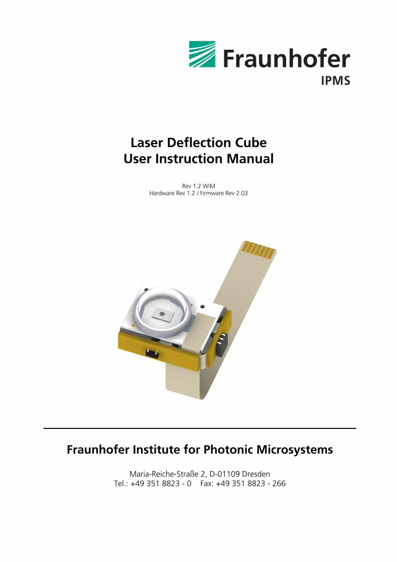
Laser Deflection Cube User Instruction Manual
Rev 1.2 WiM
Hardware Rev 1.2 / Firmware Rev 2.03
Fraunhofer Institute for Photonic Microsystems
Maria-Reiche-Straße 2, D-01109 Dresden Tel.: +49 351 8823 - 0 Fax: +49 351 8823 - 266

Laser Deflection Cube Revision 1.2, WiM
28.06.2011
Copyright © 2011, Fraunhofer IPMS 3
Table of Contents
1 ....................................................................................................5 SAFETY INSTRUCTIONS
2 ...................................................................................................6 PREPARATION FOR USE
2.1 .........................................................................................................6 Delivery Contents
2.2 ....................................................................................................................6 Unpacking
2.3 ................................................................6 Connecting scan head with driver electronics
2.4 .......................................................................................................6 Start-up procedure
3 ......................................................................................................................7 SCAN HEAD
3.1 ..........................................................................................................................7 Layout
3.2 .......................................................................7 Resonant Micro Scanning Mirror Theory
3.2.1 ..................................................................................9 Position Feedback Sensor Theory
4 ..................................................................................................11 DRIVING ELECTRONICS
4.1 ........................................................................................................................11 Layout
4.2 .............................................................................................................11 I/O Connector
4.3 .................................................................................................12 State Indicators Leeds
4.4 ........................................................................................13 Absolute Maximum Ratings
4.5 ...........................................................................................13 DC Voltage Specifications
5 .................................................................................................................14 PC INTERFACE
5.1 ..................................................................................................14 System requirements
5.2 ......................................................................14 SPI-USB adapter PICkit Serial analyzer
5.3 ..............................................................................................15 Graphical User Interface
5.4 ........................................................................................................16 LDC Interface API
5.4.1 ...................................................................................................17 Command reference
5.4.2 .....................................................................................25 LDC Interface API Error Codes
5.4.3 ..............................................................................................................26 Code sample
6 ................................................................................................................27 SPI INTERFACE
6.1 ...................................................................................27 Interface Hardware Description
6.2 ..................................................................................................28 Timing Characteristic
6.3 .................................................................................................29 Transmission Protocol
6.4 ............................................................................................................30 Error Handling
6.5 ..............................................................................................................31 Data Formats
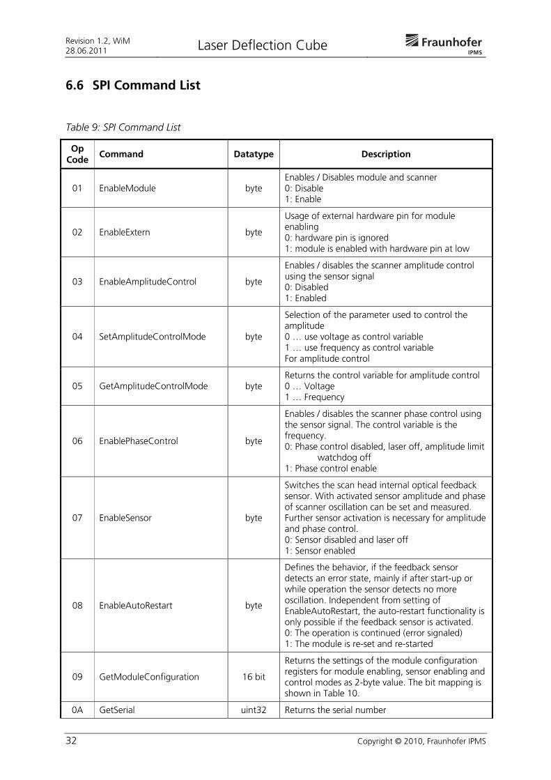
6.6 .......................................................................................................32 SPI Command List

Revision 1.2, WiM 28.06.2011 Laser Deflection Cube
4 Copyright © 2010, Fraunhofer IPMS
Laser Deflection Cube Revision 1.2, WiM
28.06.2011
Copyright © 2011, Fraunhofer IPMS 5
1 Safety Instructions
Laser Safety
Laser class II implemented = 650 nm P < 1 mW Laser emits towards the back-side of scanner mirror.
Do not disassemble scan head.
Do not use with missing scanner mirror.
No consumer product
Operation by trained personnel only.
High Voltage
200 V / 2.5 mA
Do not touch electronic board, if powered. The maximum amount of energy stored in the converter is less than 50 mJ below any hazardous levels.
ESD
The LDC scan head as well as the driver electronics, uses semiconductors that can be damaged by electrostatic discharge (ESD). When handling, care must be taken so that the devices are not damaged. The following precautions must be taken:
Do not open the protective conductive packaging until being at an approved anti-static work station.
Use a conductive wrist strap attached to a good earth ground.
Always discharge yourself by touching a grounded bare metal surface or approved anti-static mat before picking up an ESD - sensitive electronic component.
Use an approved anti-static mat to cover your work surface.
Revision 1.2, WiM 28.06.2011 Laser Deflection Cube
6 Copyright © 2010, Fraunhofer IPMS
2 Preparation for use
2.1 Delivery Contents
Scan head Driving electronics Power adaptor PICKit Serial Analyzer SPI-USB interface USB cable CD with API and application software
2.2 Unpacking
The scan head has to be handled carefully. The scan head as well as the electronic board has to be handled solely in an ESD qualified environment.
2.3 Connecting scan head with driver electronics
To realize a very small form factor of the scan head, the connection to the driver electronic board is implemented as a plug-less FPC (Flexible Printed Circuit) connection with 1 mm pitch. The connecting needs caution especially while inserting the flex tail into the jack. To avoid damaging of the flex tail and the pins, pull the lever approx. 1 mm out of the jack until a mechanical stop is noticeable. After, insert the flex tail with pins downwards into the jack and carefully close the lever. Never bend the flex tail with a radius smaller than 5 mm!
2.4 Start-up procedure
The LDC module driving electronics is factory configured to start the scanner at the specified frequency and amplitude after powering-up by connecting the power supply. The wire of electronic board is unmistakably reverse polarity protected matching to the delivered power supply. To change the scan amplitude the PC interface (see chapter 5) can be used.

Laser Deflection Cube Revision 1.2, WiM
28.06.2011
Copyright © 2011, Fraunhofer IPMS 7
3 Scan Head
3.1 Layout
Figure 1: Scan head layout
22approx.
16ap
prox
.
7,5
7,5
R6
6,1812,6
60
14,96,75
212,25M2
M2
Scan axis
R5
Figure 2: Drawing LDC scan head
3.2 Resonant Micro Scanning Mirror Theory
The scan head contains as the key component a MEMS micro scanning mirror, designed for periodical deflection of light. The scanner chip (Figure 3) is fabricated at the Fraunhofer IPMS using CMOS compatible technology. It consists of a 30 to 75 μm thick plate, suspended by two torsional springs. The optical reflection coefficient is enhanced by a thin layer of aluminum. The edges between fixed frame and moving mirror plate are formed as comb-electrodes. The membrane with the mechanical active structures is carried by a patterned bulk silicone.
Scan direction
Flexible FPC Connector
Position Feedback Sensor
Glass Dome
MEMS Scanner Mirror

Revision 1.2, WiM 28.06.2011 Laser Deflection Cube
8 Copyright © 2010, Fraunhofer IPMS
Figure 3: Exemplary design of a micro scanner mirror
The vertical sides of the comb like driving electrodes and of the mirror plate form a variable capacitance. The oscillation of the plate is excited resonantly with the double mechanical oscillation frequency. An applied voltage creates an electrostatic torque which accelerates the plate towards its rest position. To prevent a deceleration of the plate’s movement after passing the rest position the voltage between the electrodes must be switched to zero at zero crossing. At the maximum deflection angle the voltage is switched on again. A typical resonance curve is shown in figure 3. The asymmetric behavior is explained by the deceleration and therewith the collapse of oscillation due to a remaining electrostatic torque after passing rest position. This always occurs for driving frequencies smaller than the double mechanical resonance frequency. The resonance curve shows a hysteresis. Therefore, different parts of the curve are obtained dependent from the direction of the frequency sweep. The largest deflection angle will be achieved, applying a frequency sweep starting with a frequency higher than a type-specific frequency f2 down to a frequency slightly higher than the resonance frequency f1. This start-up procedure is already implemented in the firmware of the driving electronics. Due to the in-plane electrode configuration this scanner design is not suitable to achieve a static deflection.
Figure 4: MEMS micro scanner resonance behavior
After the start-up procedure, the amplitude of the scanner can be controlled theoretically by both, the voltage and the frequency of the drive signal. Using the frequency as controlled parameter, one has to take care that the frequency always has to be larger than the resonance frequency, otherwise the oscillation aborts. To avoid this state, especially in view of the fact that
0.4 0.6 0.8 1.0 1.20
f2f1
defle
ctio
n a
ngle
fexc
Anchor
Spring
Comb Drive
Insulation Trench
Laser Deflection Cube Revision 1.2, WiM
28.06.2011
Copyright © 2011, Fraunhofer IPMS 9
the resonance frequency can be slightly shifting under changing environmental conditions, normally the phase of the mirror oscillation is controlled instead. Utilizing a phase controlled operation; the coupling efficiency for the driving signal is maximal at a minimal phase (running near the mechanical resonance of the scanner). This causes the lowest possible driving voltage and thereby the lowest power consumption of the driving circuit. On the other hand, the oscillation frequency wills then slightly changing depending on the environmental conditions. Due to a steep rise of the frequency response curve near resonance, changing conditions effects also a drift of the deflection amplitude. To obtain a certain deflection in practice, the amplitude is always controlled by the driving voltage. The phase control can be used additionally to reduce the necessary driving voltage. All these driving theory aspects are implemented in the delivered driving electronics.
3.2.1 Position Feedback Sensor Theory
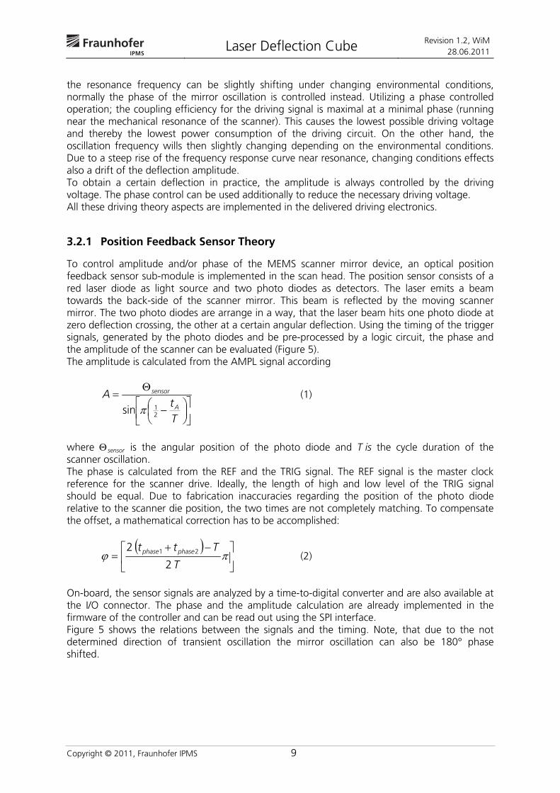
To control amplitude and/or phase of the MEMS scanner mirror device, an optical position feedback sensor sub-module is implemented in the scan head. The position sensor consists of a red laser diode as light source and two photo diodes as detectors. The laser emits a beam towards the back-side of the scanner mirror. This beam is reflected by the moving scanner mirror. The two photo diodes are arrange in a way, that the laser beam hits one photo diode at zero deflection crossing, the other at a certain angular deflection. Using the timing of the trigger signals, generated by the photo diodes and be pre-processed by a logic circuit, the phase and the amplitude of the scanner can be evaluated (Figure 5). The amplitude is calculated from the AMPL signal according
Tt
AA
sensor
21sin
(1)
where sensor is the angular position of the photo diode and T is the cycle duration of the scanner oscillation. The phase is calculated from the REF and the TRIG signal. The REF signal is the master clock reference for the scanner drive. Ideally, the length of high and low level of the TRIG signal should be equal. Due to fabrication inaccuracies regarding the position of the photo diode relative to the scanner die position, the two times are not completely matching. To compensate the offset, a mathematical correction has to be accomplished:
T
Ttt phasephase
2
2 21 (2)
On-board, the sensor signals are analyzed by a time-to-digital converter and are also available at the I/O connector. The phase and the amplitude calculation are already implemented in the firmware of the controller and can be read out using the SPI interface. Figure 5 shows the relations between the signals and the timing. Note, that due to the not determined direction of transient oscillation the mirror oscillation can also be 180° phase shifted.

Revision 1.2, WiM 28.06.2011 Laser Deflection Cube
10 Copyright © 2010, Fraunhofer IPMS
Figure 5: Sensor Signal Timing Characteristic Diagram
Table1: Position feedback sensor characteristic
Symbol Characteristic Min Typ. Max Units Conditions
Laser Wavelength 645 655 660 nm
Laser Deflection Cube Revision 1.2, WiM
28.06.2011
Copyright © 2011, Fraunhofer IPMS 11
4 Driving Electronics
The driving electronics is designed to run the LDC module either independently or under permanent data exchange with a controlling PC.
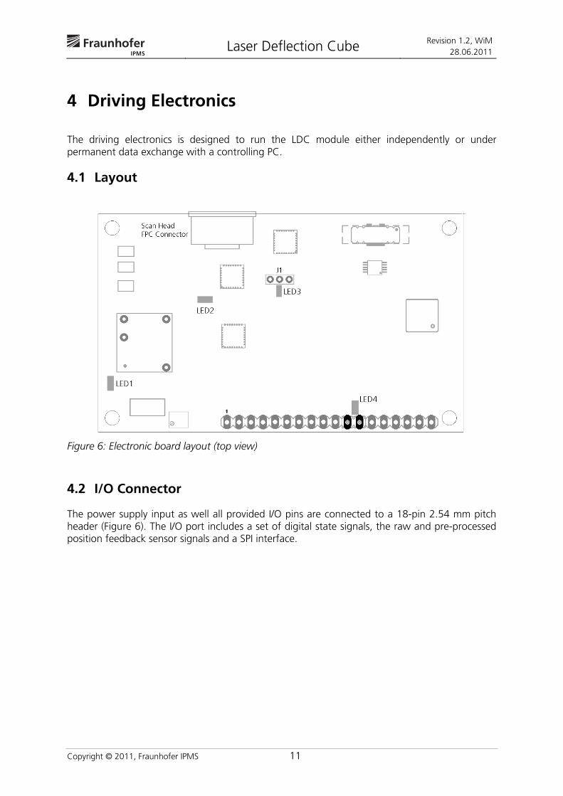
4.1 Layout
Figure 6: Electronic board layout (top view)
4.2 I/O Connector
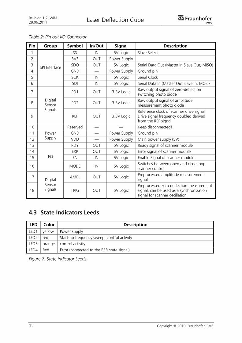
The power supply input as well all provided I/O pins are connected to a 18-pin 2.54 mm pitch header (Figure 6). The I/O port includes a set of digital state signals, the raw and pre-processed position feedback sensor signals and a SPI interface.
Revision 1.2, WiM 28.06.2011 Laser Deflection Cube
12 Copyright © 2010, Fraunhofer IPMS
Table 2: Pin out I/O Connector
Pin Group Symbol In/Out Signal Description
1 SS IN 5V Logic Slave Select
2 3V3 OUT Power Supply
3 SDO OUT 5V Logic Serial Data Out (Master In Slave Out, MISO)
4 GND — Power Supply Ground pin
5 SCK IN 5V Logic Serial Clock
6
SPI Interface
SDI IN 5V Logic Serial Data In (Master Out Slave In, MOSI)
7 PD1 OUT 3.3V Logic Raw output signal of zero-deflection switching photo diode
8 PD2 OUT 3.3V Logic Raw output signal of amplitude measurement photo diode
9
Digital Sensor Signals
REF OUT 3.3V Logic Reference clock of scanner drive signal Drive signal frequency doubled derived from the REF signal
10 Reserved — — Keep disconnected!
11 GND — Power Supply Ground pin
12
Power Supply VDD — Power Supply Main power supply (5V)
13 RDY OUT 5V Logic Ready signal of scanner module
14 ERR OUT 5V Logic Error signal of scanner module
15 EN IN 5V Logic Enable Signal of scanner module
16
I/O
MODE IN 5V Logic Switches between open and close loop scanner control
17 AMPL OUT 5V Logic Preprocessed amplitude measurement signal
18
Digital Sensor Signals TRIG OUT 5V Logic
Preprocessed zero deflection measurement signal, can be used as a synchronization signal for scanner oscillation
4.3 State Indicators Leeds
LED Color Description
LED1 yellow Power supply
LED2 red Start-up frequency sweep, control activity
LED3 orange control activity
LED4 Red Error (connected to the ERR state signal)
Figure 7: State indicator Leeds
Laser Deflection Cube Revision 1.2, WiM
28.06.2011
Copyright © 2011, Fraunhofer IPMS 13
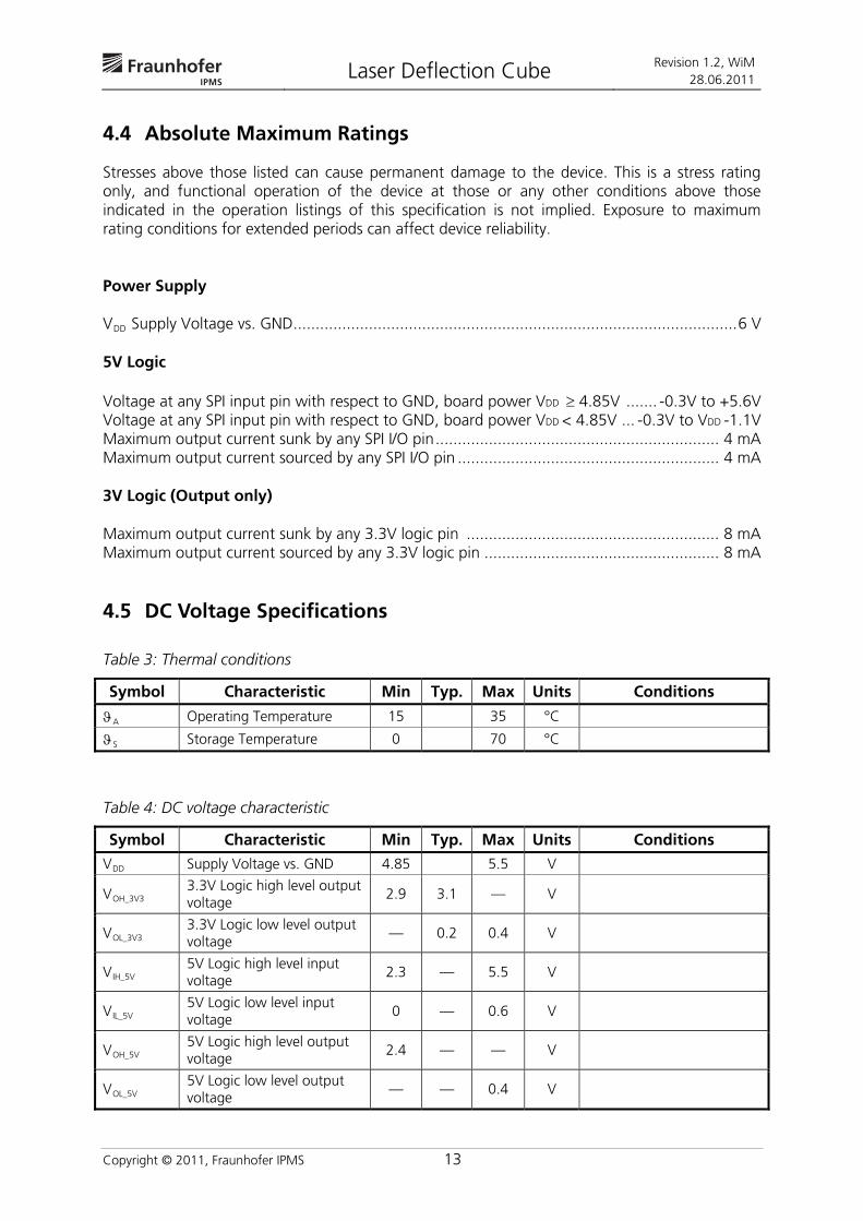
4.4 Absolute Maximum Ratings
Stresses above those listed can cause permanent damage to the device. This is a stress rating only, and functional operation of the device at those or any other conditions above those indicated in the operation listings of this specification is not implied. Exposure to maximum rating conditions for extended periods can affect device reliability. Power Supply VDD Supply Voltage vs. GND....................................................................................................6 V 5V Logic Voltage at any SPI input pin with respect to GND, board power VDD 4.85V ....... -0.3V to +5.6V Voltage at any SPI input pin with respect to GND, board power VDD < 4.85V ... -0.3V to VDD -1.1V Maximum output current sunk by any SPI I/O pin................................................................ 4 mA Maximum output current sourced by any SPI I/O pin ........................................................... 4 mA 3V Logic (Output only) Maximum output current sunk by any 3.3V logic pin ......................................................... 8 mA Maximum output current sourced by any 3.3V logic pin ..................................................... 8 mA
4.5 DC Voltage Specifications
Table 3: Thermal conditions
Symbol Characteristic Min Typ. Max Units Conditions
A Operating Temperature 15 35 °C
S Storage Temperature 0 70 °C
Table 4: DC voltage characteristic
Symbol Characteristic Min Typ. Max Units Conditions
VDD Supply Voltage vs. GND 4.85 5.5 V
VOH_3V3 3.3V Logic high level output voltage
2.9 3.1 — V
VOL_3V3 3.3V Logic low level output voltage
— 0.2 0.4 V
VIH_5V 5V Logic high level input voltage
2.3 — 5.5 V
VIL_5V 5V Logic low level input voltage
0 — 0.6 V
VOH_5V 5V Logic high level output voltage
2.4 — — V
VOL_5V 5V Logic low level output voltage
— — 0.4 V
Revision 1.2, WiM 28.06.2011 Laser Deflection Cube
14 Copyright © 2010, Fraunhofer IPMS
5 PC Interface
The LDC module driving electronics can be controlled optionally from a PC running on Windows XP or later. In delivery there is included a SPI – USB adapter, which is directly connectable to LDC module driving electronics, an USB cable, an interface API and a simple application which can control the LDC module easily.
5.1 System requirements
Windows XP, Vista, 7 .NET framework 2.0 (2.0.50727) or later USB 2.0 For LDC interface API: Software development environment supporting .NET like Visual
Studio 2005 (Express) or later, LabView 8 or later)
5.2 SPI-USB adapter PICkit Serial analyzer
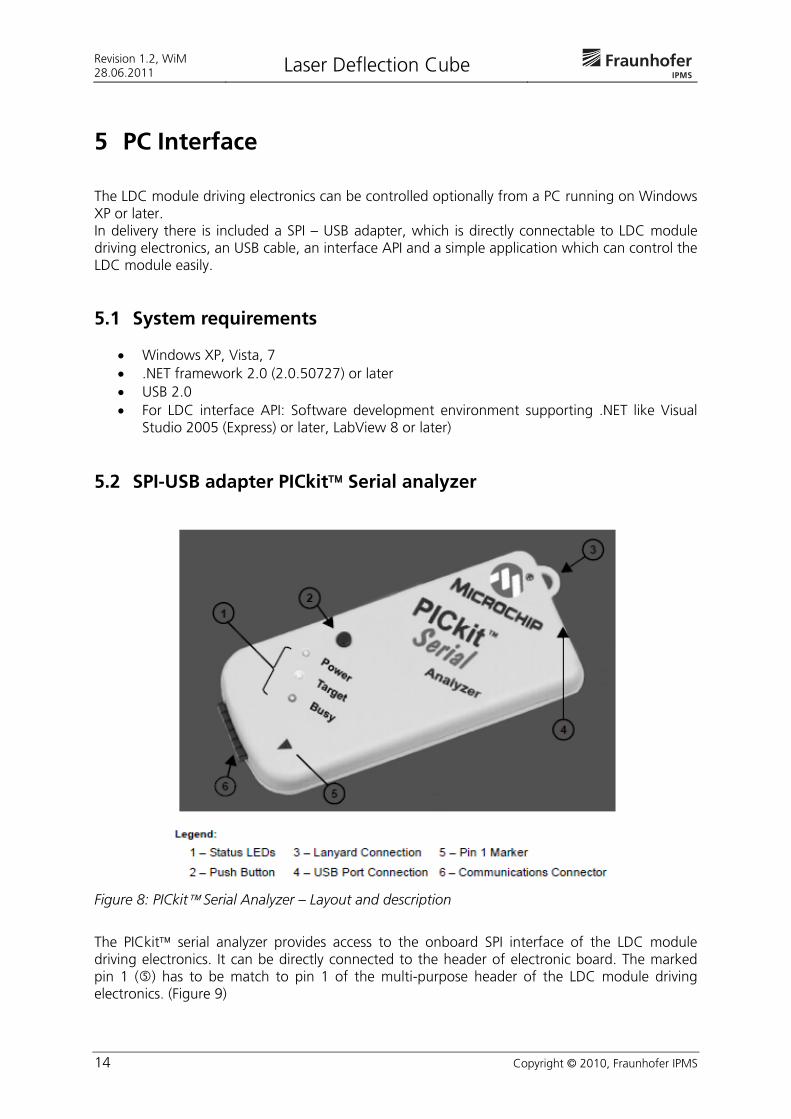
Figure 8: PICkit Serial Analyzer – Layout and description
The PICkit serial analyzer provides access to the onboard SPI interface of the LDC module driving electronics. It can be directly connected to the header of electronic board. The marked pin 1 () has to be match to pin 1 of the multi-purpose header of the LDC module driving electronics. (Figure 9)
Laser Deflection Cube Revision 1.2, WiM
28.06.2011
Copyright © 2011, Fraunhofer IPMS 15
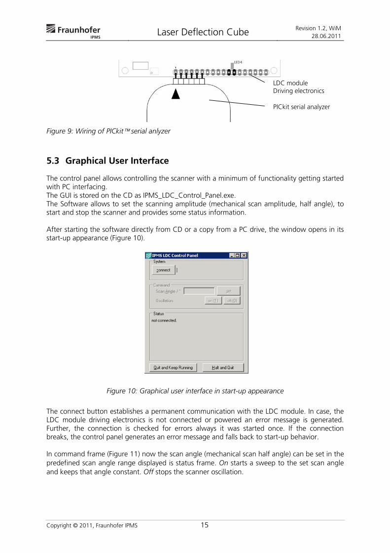
Figure 9: Wiring of PICkit serial anlyzer
5.3 Graphical User Interface
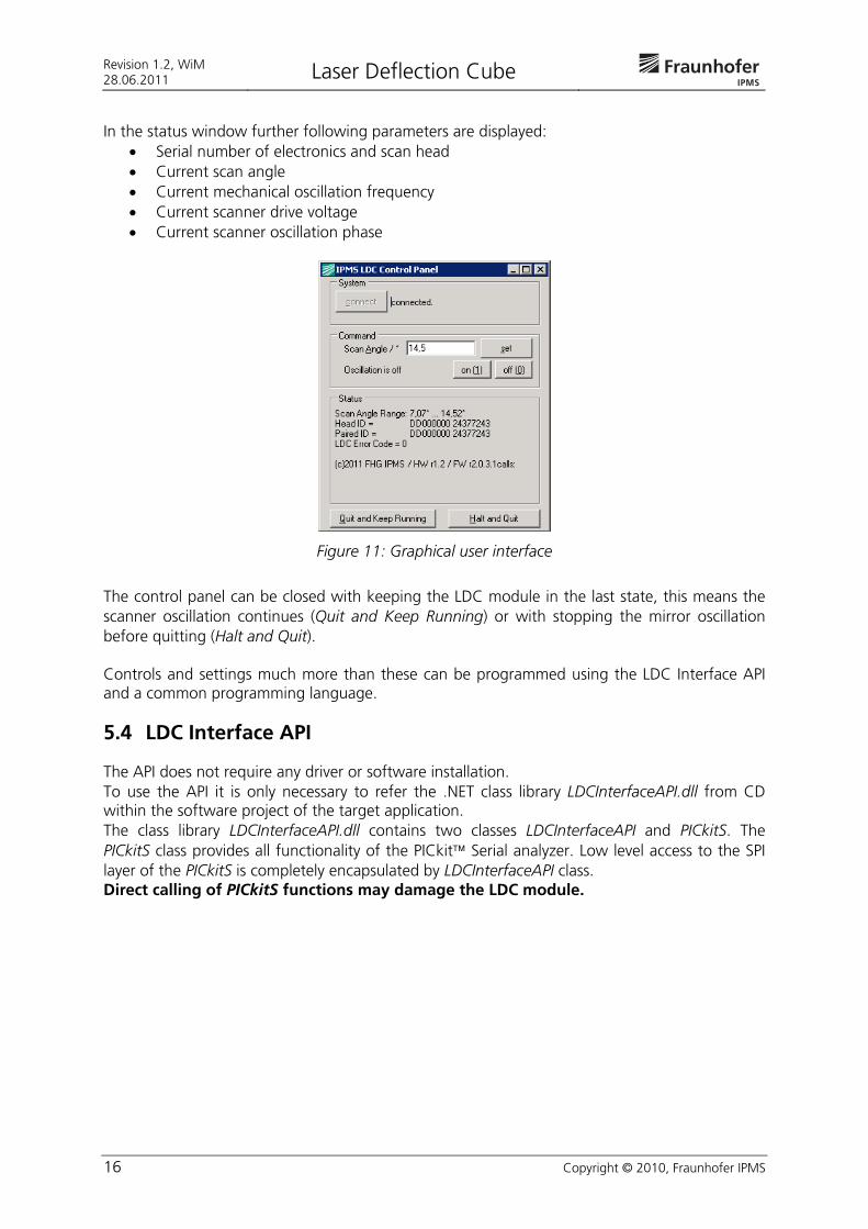
The control panel allows controlling the scanner with a minimum of functionality getting started with PC interfacing. The GUI is stored on the CD as IPMS_LDC_Control_Panel.exe. The Software allows to set the scanning amplitude (mechanical scan amplitude, half angle), to start and stop the scanner and provides some status information. After starting the software directly from CD or a copy from a PC drive, the window opens in its start-up appearance (Figure 10).
Figure 10: Graphical user interface in start-up appearance
The connect button establishes a permanent communication with the LDC module. In case, the LDC module driving electronics is not connected or powered an error message is generated. Further, the connection is checked for errors always it was started once. If the connection breaks, the control panel generates an error message and falls back to start-up behavior. In command frame (Figure 11) now the scan angle (mechanical scan half angle) can be set in the predefined scan angle range displayed is status frame. On starts a sweep to the set scan angle and keeps that angle constant. Off stops the scanner oscillation.
PICkit serial analyzer
LDC module Driving electronics
Revision 1.2, WiM 28.06.2011 Laser Deflection Cube
16 Copyright © 2010, Fraunhofer IPMS
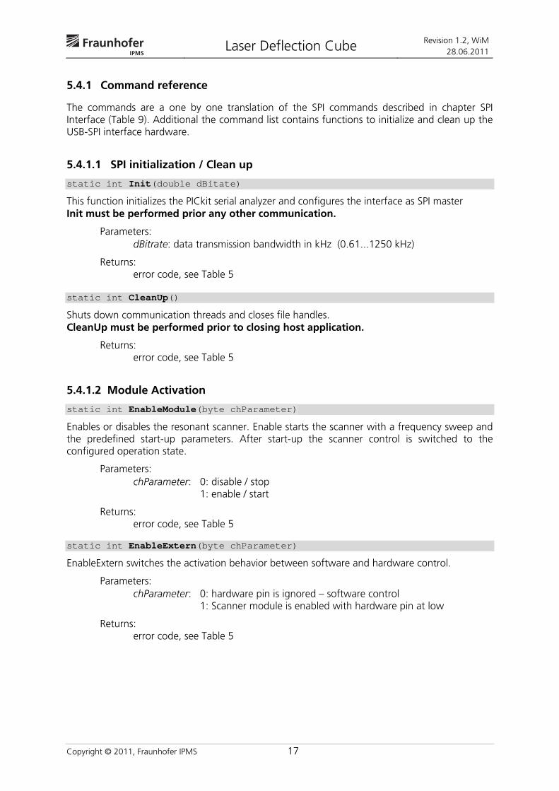
In the status window further following parameters are displayed: Serial number of electronics and scan head Current scan angle Current mechanical oscillation frequency Current scanner drive voltage Current scanner oscillation phase
Figure 11: Graphical user interface
The control panel can be closed with keeping the LDC module in the last state, this means the scanner oscillation continues (Quit and Keep Running) or with stopping the mirror oscillation before quitting (Halt and Quit). Controls and settings much more than these can be programmed using the LDC Interface API and a common programming language.
5.4 LDC Interface API
The API does not require any driver or software installation. To use the API it is only necessary to refer the .NET class library LDCInterfaceAPI.dll from CD within the software project of the target application. The class library LDCInterfaceAPI.dll contains two classes LDCInterfaceAPI and PICkitS. The PICkitS class provides all functionality of the PICkit Serial analyzer. Low level access to the SPI layer of the PICkitS is completely encapsulated by LDCInterfaceAPI class. Direct calling of PICkitS functions may damage the LDC module.
Laser Deflection Cube Revision 1.2, WiM
28.06.2011
Copyright © 2011, Fraunhofer IPMS 17
5.4.1 Command reference
The commands are a one by one translation of the SPI commands described in chapter SPI Interface (Table 9). Additional the command list contains functions to initialize and clean up the USB-SPI interface hardware.
5.4.1.1 SPI initialization / Clean up
static int Init(double dBitate)
This function initializes the PICkit serial analyzer and configures the interface as SPI master Init must be performed prior any other communication.
Parameters: dBitrate: data transmission bandwidth in kHz (0.61...1250 kHz)
Returns: error code, see Table 5
static int CleanUp()
Shuts down communication threads and closes file handles. CleanUp must be performed prior to closing host application.
Returns: error code, see Table 5
5.4.1.2 Module Activation
static int EnableModule(byte chParameter)
Enables or disables the resonant scanner. Enable starts the scanner with a frequency sweep and the predefined start-up parameters. After start-up the scanner control is switched to the configured operation state.
Parameters: chParameter: 0: disable / stop 1: enable / start
Returns: error code, see Table 5
static int EnableExtern(byte chParameter)
EnableExtern switches the activation behavior between software and hardware control.
Parameters: chParameter: 0: hardware pin is ignored – software control 1: Scanner module is enabled with hardware pin at low
Returns: error code, see Table 5

Revision 1.2, WiM 28.06.2011 Laser Deflection Cube
18 Copyright © 2010, Fraunhofer IPMS
5.4.1.3 Resonance scanner parameters
static int SetAmplitude(float fValue) static int GetAmplitude(byte chParameter, out float fValue)
Mechanical scan amplitude (MSA) in degree. The SetAmplitude function sets the target for the amplitude control. The GetAmplitude function returns the target or the current value depending on the parameter. Note: Feedback sensor must be switched on and amplitude control must be enabled. Otherwise the amplitude will not be controlled.
Parameters: fValue: target value for the amplitude control chParameter: 0: current mechanical scan amplitude (MSA) in degree 1: mean mechanical scan amplitude (MSA) in degree
2: current raw value in ns 3: mean raw value in ns
4: target mechanical scan amplitude (MSA) in degree 5: target value in ns
Returns: error code, see Table 5
fValue (out): value corrensponding to the transmitted parameter
static int GetAmplitudeLimits(out float fMinValue, out float fMaxValue)
Returns the factory-defined range for amplitude values, the minimum and the maximum. The limits represents the parameter input range and the range of a internal watchdog. Electronics switches to an error state if the limit is achieved.
Returns: error code, see Table 5
fMinValue: minimum fMaxValue: maximum
static int SetPhase(float fValue) static int GetPhase(byte chParameter, out float fValue)
Phase of the scanner oscillation respective to the drive signal. The SetPhase function sets the target for the phase control. The GetPhase function returns the target or the current value depending on the parameter. Note: Feedback sensor must be switched on and amplitude control must be enabled. Otherwise the amplitude will not be controlled.
Parameters: fValue: target value for the phase control chParameter: 0: current value in degree 1: mean value in degree 2: current raw value in ns 3: mean raw value in ns 4: target value in degree 5: target value in ns
Returns: error code, see Table 5
fValue (out): value corrensponding to the transmitted parameter
Laser Deflection Cube Revision 1.2, WiM
28.06.2011
Copyright © 2011, Fraunhofer IPMS 19
static int GetPhaseLimits(out float fMinValue, out float fMaxValue)
Returns the factory-defined range for phase values, the minimum and the maximum. The limits represents the parameter input range and the range of a internal watchdog. Electronics switches to an error state if the limit is achieved.
Returns: error code, see Table 5
fMinValue: minimum fMaxValue: maximum
static int SetVoltage(float fValue) static int GetVoltage(out float fValue) Peak to peak voltage of the resonance scanner drive signal. Note: The Voltage is not stored in EEPROM. On Power-up the scanner starts with the pre-configured start-up voltage. A voltage, set in idle mode (module disabled), is overwritten by pre-defined start-up parameters if the scanner is enabled. Setting voltage during scanner start-up is denied and returns illegal command. Setting voltage directly in amplitude and phase control mode is not interlocked but strictly not recommended. SetVoltage can be inactivated in the some customized module configuration.
Parameters: fValue: voltage in V
Returns: error code, see Table 5 fValue (out): current voltage in V
static int GetVoltageLimits(out float fMinValue, out float fMaxValue)
Returns the factory-defined range for voltage values, the minimum and the maximum [V]. The limits define the parameter input range. Furthermore the internal amplitude control (control variable: voltage) is limited to this range.
Returns: error code, see Table 5
fMinValue: minimum fMaxValue: maximum
static int SetFrequency(float fValue) static int GetFrequency(out float fValue)
Sets and returns the frequency of scanner drive signal in Hz. The drive frequency is double the mechanical oscillation frequency. This frequency setting is only possible if phase control is disabled and amplitude control is in voltage mode or disabled. Note: The frequency is not stored in EEPROM. On power-up the scanner starts with the pre-configured start-up frequency. A frequency, set in idle mode (module disabled), is overwritten by pre-defined start-up parameters if the scanner is enabled. Setting frequency during scanner start-up is denied and returns illegal command. Setting frequency directly in amplitude and phase control mode is not interlocked but strictly not recommended.
Revision 1.2, WiM 28.06.2011 Laser Deflection Cube
20 Copyright © 2010, Fraunhofer IPMS
SetFrequency can be inactivated in the some customized module configuration. Parameters:
Value: frequency
Returns: error code, see Table 5
fValue (out): current frequency of resonance scanner drive static int GetFrequencyLimits(out float fMinValue, out float fMaxValue)
Returns the defined range for frequency values, the minimum and the maximum in Hz.
Returns: error code, see Table 5
fMinValue: minimum fMaxValue: maximum
static int GetResonanceFrequency(out float fValue)
Returns the resonance frequency of the MEMS scanner, stored in EEPROM [Hz]. The limits define the parameter input range.
Returns: error code, see Table 5
fValue: eesonance frequency
5.4.1.4 Optical feedback sensor and control
static int EnableSensor(byte chParameter)
Switches the scan head internal optical feedback sensor. With activated sensor amplitude and phase of scanner oscillation can be set and measured. Further sensor activation is necessary for amplitude and phase control. Function EnableSensor can be inactivated in the some customized module configuration. Parameters:
chParameter: 0: Sensor disabled and laser off 1: Sensor
Returns: error code, see Table 5
static int EnableAmplitudeControl(byte chParameter)
Enables / disables the scanner amplitude control using the feedback sensor signal. Disabling amplitude control can be prohibited in the some customized module configuration.
Parameters: chParameter: 0: amplitude control disabled, amplitude regulation via voltage or
frequency 1: amplitude control is enabled
Returns: error code, see Table 5
Laser Deflection Cube Revision 1.2, WiM
28.06.2011
Copyright © 2011, Fraunhofer IPMS 21
static int SetAmplitudeControlMode(byte chParameter) static int GetAmplitudeControlMode(out byte chValue)
AmplitudeControlMode mode selects the parameter, the amplitude is controlled with. This function can be inactivated in the some customized module configuration.
Parameters: chParameter: 0: … use voltage as control variable 1: … use frequency as control variable Returns:
error code, see Table 5 chValue: 0: … use voltage as control variable 1: … use frequency as control variable
static int EnablePhaseControl(byte chParameter)
Enables / disables the scanner phase control using the feedback sensor signal. Disabling phase control can be prohibited in the customized module configuration.
Parameters: chParameter: 0: phase control disabled 1: phase control is enabled
Returns: error code, see Table 5
static int EnableAutoRestart(byte chParameter)
Defines the behavior, if the feedback sensor detects an error state, mainly if after start-up or while operation the sensor detects no more oscillation. Independent from setting of EnableAutoRestart, the auto-restart functionality is only possible if the feedback sensor is activated.
Parameters: chParameter: 0: The current operation of the scanner is continued and an error
is signaled 1: The module is re-set and re-started
Returns: error code, see Table 5
static int GetModuleConfiguration(out UInt16 nValue)
Returns the settings of the module configuration registers for module enabling, sensor enabling and control modes as 2-byte value. The bit mapping is shown in
Revision 1.2, WiM 28.06.2011 Laser Deflection Cube
22 Copyright © 2010, Fraunhofer IPMS
Table 10.
Returns: error code, see Table 5
nValue: see
Laser Deflection Cube Revision 1.2, WiM
28.06.2011
Copyright © 2011, Fraunhofer IPMS 23
Table 10
static int GetControlState(out byte chValue)
Returns in the state of the scanner oscillation, amplitude control and phase control. If a value (phase or amplitude) is changed, the assigned bit is set to 0. If the scanner oscillation is on target the bit is set to 1.
Returns: error code, see Table 5 chValue: see Table 11
5.4.1.5 Diagnostics
static int GetSerial(out UInt32 nValue)
Returns a unique serial number of the LDC-Module.
Returns: error code, see Table 5 nValue: serial number
static int GetVersion(out string szValue)
Returns the firmware version of the LDC module driving electronics.
Returns: error code, see see Table 5 szValue: string with the firmware version
static int GetState(out byte chValue)
Returns the current state of the internal state machine.
Returns: error code, see Table 5
chValue: state, see
Revision 1.2, WiM 28.06.2011 Laser Deflection Cube
24 Copyright © 2010, Fraunhofer IPMS
Table 10.
static int GetErrorCode(out byte chValue)
Returns the error code of the last error detected by the LDC driving electronics
Returns: error code of the function, see Table 5 chValue: see Table 12
5.4.1.6 Storing of settings
static int EEPROM(byte chParameter)
Stores and loads the configuration to or from the electronic internal EEPROM.
Parameters: chParameter: 0: Store 1: Load
Returns: error code of the function, see Table 5
5.4.1.7 Low-level functions
Low level fuctions are not needed to call directly for a communication with the LDC module. static int TransmitFrame(byte chOpCode, byte[] chTXData, out byte[] chRXData) Low level function to transmit data frames to the LDC module. The function is not necessary for the user to communicate with the LDC module. It is called from the SetCommand/GetCommand function and can be used for own low-level access to the SPI protocol.
Parameters: chOpCode: SPI command code, see table 6, Manual Laser Deflection Cube
Returns: chTXData: Data to transmit to LDC module chRXData: Data to receive from LDC module
Returns: error code of the function, see Table 5
Note: Data length of the arrays must be match with the transmitted data type (table 6, Manual Laser Deflection Cube) static int GetCommand(byte chOpCode,out…) static int SetCommand(byte bOpCode,…) The functions GetCommand / Set Command can be used to call a function via its OpCode. Types of parameter are identical to upper description.
Parameters: chOpCode: SPI command code, see Table 9
Returns: error code of the function, see Table 5
Laser Deflection Cube Revision 1.2, WiM
28.06.2011
Copyright © 2011, Fraunhofer IPMS 25
5.4.2 LDC Interface API Error Codes
Table 5: LDC Interface API Error Codes
Wert Name Beschreibung
0 No error
1 SPI_ERROR_PICKIT PICKit inizialization error, e.g. not connected
2 SPI_ERROR_BUSY LDC module driving electronics busy Try again
3 SPI_ERROR_OUT_OF_RANGE Values are out of range in a Set Command Check the limits
4 SPI_ERROR_ILLEGAL_COMMAND Command not allowed in this context
5 SPI_ERROR_ACCESS_DENIED
Command is not accessible in this customized configuration. The LDC module driving electronics covers a wide range of scanners and applications. To avoid damaging certain not usefull commands are denied.
6 SPI_ERROR_CRC Via SPI transmited data frames are corrupted. Reduction of data transmission bitrate (see 5.4.1.1) Reduction of cable length
7 SPI_ERROR_TIMEOUT Command reply timout Reduction of data transmission bitrate (see 5.4.1.1) Reduction of cable length
8 ERROR_DATA_LENGTH An other data length was expected Error can only occur with low level commands
9 ERROR_INIT_PKSA Hardware error of PICKit serial analyzer while initialization
10 ERROR_INIT_SPI Hardware error of PICKit serial analyzer while initialization of the SPI interface application
11 ERROR_INIT Error while initalization of SPI communication
13 ERROR_WRONG_PKSA_FW Firmware version of PICKit serial is to low for this application
14 ERROR_BITRATE Bitrate tranmitted with command Init is not valid
15 SPI_ERROR_ENDTOKEN No transmission frame end token received Reduction of data transmission bitrate (see 5.4.1.1) Reduction of cable length

Revision 1.2, WiM 28.06.2011 Laser Deflection Cube
26 Copyright © 2010, Fraunhofer IPMS
5.4.3 Code sample
The following code (C#, Microsoft Visual Studio 2005) initializes the PICkit and the SPI Interface, activates the scanner and reads out the actual voltage. Last, the PICkit interface is removed from memory.
Figure 12: Implementation of LDC Interface API as class library in Microsoft Visual Studio 2005
using LDCInterfaceAPI; private void LDCFunction() { int ret; ret = LDCInterface.Init(1000); if (ret!=0) MessageBox.Show("Error initializing PICKit Serial. Error "+ret); ret = LDCInterface.EnableModule(1); if (ret!=0) MessageBox.Show("Error enabling scanner. Error "+ret); float Voltage; ret = LDCInterface.GetVoltage(out Voltage); if (ret!=0) MessageBox.Show("Error reading voltage. Error "+ret); MessageBox.Show("Current Voltage: "+Voltage); LDCInterface.CleanUp; }
Laser Deflection Cube Revision 1.2, WiM
28.06.2011
Copyright © 2011, Fraunhofer IPMS 27
6 SPI Interface
6.1 Interface Hardware Description
The LDC electronic board provides a Serial Peripheral Interface (SPI) interface to configure the control of the micro scanner device and to receive operational status information of the scanner and the position feedback sensor by a superordinated system controller. The SPI interface of the on-board digital signal controller is electrically connected directly to the edge connector of the board. The SPI interface is configured to run in slave mode. This means, that both, the Serial Clock (SCK) and the transmission request, controlled by Slave Select (SS) have to be provided by the SPI master device. To initiate a data transmission or reception, the SS signal must be driven low. The interface is further configured that the data transmission occurs at the rising edge of the high-active Serial Clock input signal (SCK). The word length of data is determined to one byte. A command frame embodies multiple bytes, so the SS command must be hold on low until the complete sequence is transmitted. To transmit data to the LDC board, the data must be provided at Serial Data In (SDI). Data can be read from the LDC board using the Serial Data Out Signal (SDO). Both data transmission lines are served simultaneously with the serial clock. Figure 13 shows the timing diagram of the serial communication.
Figure 13: SPI Timing Diagram
Revision 1.2, WiM 28.06.2011 Laser Deflection Cube
28 Copyright © 2010, Fraunhofer IPMS
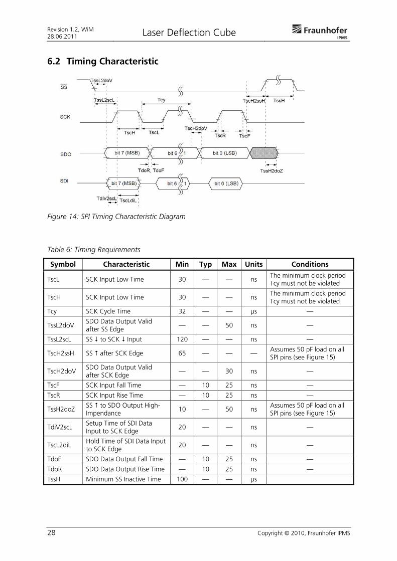
6.2 Timing Characteristic
Figure 14: SPI Timing Characteristic Diagram
Table 6: Timing Requirements
Symbol Characteristic Min Typ Max Units Conditions
TscL SCK Input Low Time 30 — — ns The minimum clock period Tcy must not be violated
TscH SCK Input Low Time 30 — — ns The minimum clock period Tcy must not be violated
Tcy SCK Cycle Time 32 — — μs —
TssL2doV SDO Data Output Valid after SS Edge
— — 50 ns —
TssL2scL SS to SCK Input 120 — — ns —
TscH2ssH SS after SCK Edge 65 — — — Assumes 50 pF load on all SPI pins (see Figure 15)
TscH2doV SDO Data Output Valid after SCK Edge
— — 30 ns —
TscF SCK Input Fall Time — 10 25 ns —
TscR SCK Input Rise Time — 10 25 ns —
TssH2doZ SS to SDO Output High- Impendance
10 — 50 ns Assumes 50 pF load on all SPI pins (see Figure 15)
TdiV2scL Setup Time of SDI Data Input to SCK Edge
20 — — ns —
TscL2diL Hold Time of SDI Data Input to SCK Edge
20 — — ns —
TdoF SDO Data Output Fall Time — 10 25 ns —
TdoR SDO Data Output Rise Time — 10 25 ns —
TssH Minimum SS Inactive Time 100 — — μs
Laser Deflection Cube Revision 1.2, WiM
28.06.2011
Copyright © 2011, Fraunhofer IPMS 29
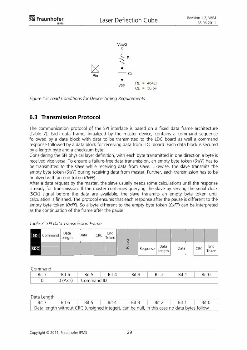
Figure 15: Load Conditions for Device Timing Requirements
6.3 Transmission Protocol
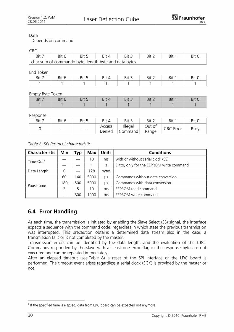
The communication protocol of the SPI interface is based on a fixed data frame architecture (Table 7). Each data frame, initialized by the master device, contains a command sequence followed by a data block with data to be transmitted to the LDC board as well a command response followed by a data block for receiving data from LDC board. Each data block is secured by a length byte and a checksum byte. Considering the SPI physical layer definition, with each byte transmitted in one direction a byte is received vice versa. To ensure a failure-free data transmission, an empty byte token (0xFF) has to be transmitted to the slave while receiving data from slave. Likewise, the slave transmits the empty byte token (0xFF) during receiving data from master. Further, each transmission has to be finalized with an end token (0xFF). After a data request by the master, the slave usually needs some calculations until the response is ready for transmission. If the master continues querying the slave by serving the serial clock (SCK) signal before the data are available, the slave transmits an empty byte token until calculation is finished. The protocol ensures that each response after the pause is different to the empty byte token (0xFF). So a byte different to the empty byte token (0xFF) can be interpreted as the continuation of the frame after the pause.
Table 7: SPI Data Transmission Frame
SDI Command Data
Length
CRC
End Token
SDO
ResponseData
Length CRC
End Token
Command
Bit 7 Bit 6 Bit 5 Bit 4 Bit 3 Bit 2 Bit 1 Bit 0 0 0 (Axis) Command ID
Data Length
Bit 7 Bit 6 Bit 5 Bit 4 Bit 3 Bit 2 Bit 1 Bit 0 Data length without CRC (unsigned integer), can be null, in this case no data bytes follow
Data
Data
Paus
e
Revision 1.2, WiM 28.06.2011 Laser Deflection Cube
30 Copyright © 2010, Fraunhofer IPMS
Data Depends on command CRC
Bit 7 Bit 6 Bit 5 Bit 4 Bit 3 Bit 2 Bit 1 Bit 0 char sum of commando byte, length byte and data bytes
End Token
Bit 7 Bit 6 Bit 5 Bit 4 Bit 3 Bit 2 Bit 1 Bit 0 1 1 1 1 1 1 1 1
Empty Byte Token
Bit 7 Bit 6 Bit 5 Bit 4 Bit 3 Bit 2 Bit 1 Bit 0 1 1 1 1 1 1 1 1
Response
Bit 7 Bit 6 Bit 5 Bit 4 Bit 3 Bit 2 Bit 1 Bit 0
0 — — Access Denied
Illegal Command
Out of Range
CRC Error Busy
Table 8: SPI Protocol characteristic
Characteristic Min Typ Max Units Conditions
— — 10 ms with or without serial clock (SS) Time-Out1
— — 1 s Ditto, only for the EEPROM write command
Data Length 0 — 128 bytes
60 140 5000 μs Commands without data conversion
180 500 5000 μs Commands with data conversion
2 5 10 ms EEPROM read command Pause time
— 800 1000 ms EEPROM write command
6.4 Error Handling
At each time, the transmission is initiated by enabling the Slave Select (SS) signal, the interface expects a sequence with the command code, regardless in which state the previous transmission was interrupted. This precaution obtains a determined data stream also in the case, a transmission fails or is not completed by the master. Transmission errors can be identified by the data length, and the evaluation of the CRC. Commands responded by the slave with at least one error flag in the response byte are not executed and can be repeated immediately. After an elapsed timeout (see Table 8) a reset of the SPI interface of the LDC board is performed. The timeout event arises regardless a serial clock (SCK) is provided by the master or not.
1 If the specified time is elapsed, data from LDC board can be expected not anymore.
Laser Deflection Cube Revision 1.2, WiM
28.06.2011
Copyright © 2011, Fraunhofer IPMS 31
6.5 Data Formats
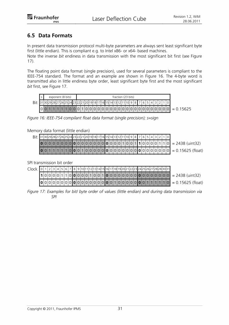
In present data transmission protocol multi-byte parameters are always sent least significant byte first (little endian). This is compliant e.g. to Intel x86- or x64- based machines. Note the inverse bit endiness in data transmission with the most significant bit first (see Figure 17). The floating point data format (single precision), used for several parameters is compliant to the IEEE-754 standard. The format and an example are shown in Figure 16. The 4-byte word is transmitted also in little endiness byte order, least significant byte first and the most significant bit first, see Figure 17.
s exponent (8 bits) fraction (23 bits) Bit 31 30 29 28 27 26 25 24 23 22 21 20 19 18 17 16 15 14 13 12 11 10 9 8 7 6 5 4 3 2 1 0
0 0 1 1 1 1 1 0 0 0 1 0 0 0 0 0 0 0 0 0 0 0 0 0 0 0 0 0 0 0 0 0 = 0.15625
Figure 16: IEEE-754 compilant float data format (single precision); s=sign
Memory data format (little endian)
Bit 31 30 29 28 27 26 25 24 23 22 21 20 19 18 17 16 15 14 13 12 11 10 9 8 7 6 5 4 3 2 1 0 0 0 0 0 0 0 0 0 0 0 0 0 0 0 0 0 0 0 0 0 1 0 0 1 1 0 0 0 0 1 1 0 = 2438 (uint32)
0 0 1 1 1 1 1 0 0 0 1 0 0 0 0 0 0 0 0 0 0 0 0 0 0 0 0 0 0 0 0 0 = 0.15625 (float)
SPI transmission bit order
Clock 0 1 2 3 4 5 6 7 8 9 10 11 12 13 14 15 16 17 18 19 20 21 22 23 24 25 26 27 28 28 30 31 1 0 0 0 0 1 1 0 0 0 0 0 1 0 0 1 0 0 0 0 0 0 0 0 0 0 0 0 0 0 0 0 = 2438 (uint32)
0 0 0 0 0 0 0 0 0 0 0 0 0 0 0 0 0 0 1 0 0 0 0 0 0 0 1 1 1 1 1 0 = 0.15625 (float)
Figure 17: Examples for bit/ byte order of values (little endian) and during data transmission via SPI
Revision 1.2, WiM 28.06.2011 Laser Deflection Cube
32 Copyright © 2010, Fraunhofer IPMS
6.6 SPI Command List
Table 9: SPI Command List
Op Code
Command Datatype Description
01 EnableModule byte Enables / Disables module and scanner 0: Disable 1: Enable
02 EnableExtern byte
Usage of external hardware pin for module enabling 0: hardware pin is ignored 1: module is enabled with hardware pin at low
03 EnableAmplitudeControl byte
Enables / disables the scanner amplitude control using the sensor signal 0: Disabled 1: Enabled
04 SetAmplitudeControlMode byte
Selection of the parameter used to control the amplitude 0 … use voltage as control variable 1 … use frequency as control variable For amplitude control
05 GetAmplitudeControlMode byte Returns the control variable for amplitude control 0 … Voltage 1 … Frequency
06 EnablePhaseControl byte
Enables / disables the scanner phase control using the sensor signal. The control variable is the frequency. 0: Phase control disabled, laser off, amplitude limit watchdog off 1: Phase control enable
07 EnableSensor byte
Switches the scan head internal optical feedback sensor. With activated sensor amplitude and phase of scanner oscillation can be set and measured. Further sensor activation is necessary for amplitude and phase control. 0: Sensor disabled and laser off 1: Sensor enabled
08 EnableAutoRestart byte
Defines the behavior, if the feedback sensor detects an error state, mainly if after start-up or while operation the sensor detects no more oscillation. Independent from setting of EnableAutoRestart, the auto-restart functionality is only possible if the feedback sensor is activated. 0: The operation is continued (error signaled) 1: The module is re-set and re-started
09 GetModuleConfiguration 16 bit
Returns the settings of the module configuration registers for module enabling, sensor enabling and control modes as 2-byte value. The bit mapping is shown in Table 10.
0A GetSerial uint32 Returns the serial number
Laser Deflection Cube Revision 1.2, WiM
28.06.2011
Copyright © 2011, Fraunhofer IPMS 33
Op Code
Command Datatype Description
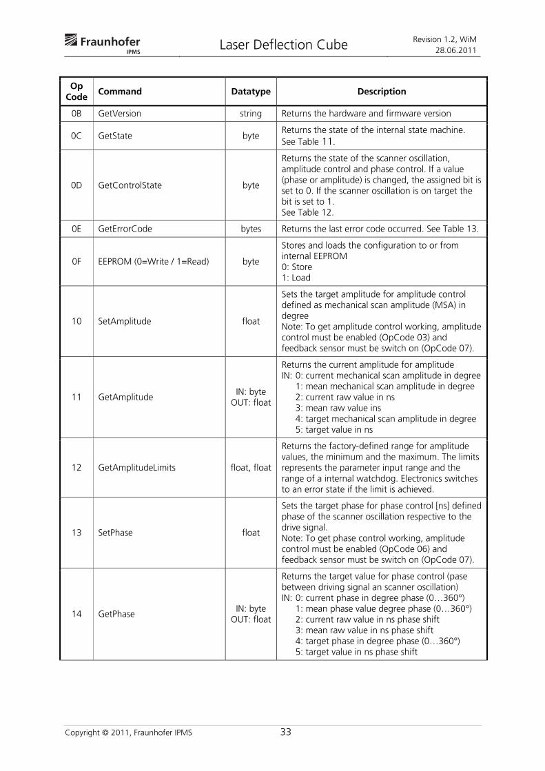
0B GetVersion string Returns the hardware and firmware version
0C GetState byte Returns the state of the internal state machine. See Table 11.
0D GetControlState byte
Returns the state of the scanner oscillation, amplitude control and phase control. If a value (phase or amplitude) is changed, the assigned bit is set to 0. If the scanner oscillation is on target the bit is set to 1. See Table 12.
0E GetErrorCode bytes Returns the last error code occurred. See Table 13.
0F EEPROM (0=Write / 1=Read) byte
Stores and loads the configuration to or from internal EEPROM 0: Store 1: Load
10 SetAmplitude float
Sets the target amplitude for amplitude control defined as mechanical scan amplitude (MSA) in degree Note: To get amplitude control working, amplitude control must be enabled (OpCode 03) and feedback sensor must be switch on (OpCode 07).
11 GetAmplitude IN: byte
OUT: float
Returns the current amplitude for amplitude IN: 0: current mechanical scan amplitude in degree 1: mean mechanical scan amplitude in degree 2: current raw value in ns 3: mean raw value ins 4: target mechanical scan amplitude in degree 5: target value in ns
12 GetAmplitudeLimits float, float
Returns the factory-defined range for amplitude values, the minimum and the maximum. The limits represents the parameter input range and the range of a internal watchdog. Electronics switches to an error state if the limit is achieved.
13 SetPhase float
Sets the target phase for phase control [ns] definedphase of the scanner oscillation respective to the drive signal. Note: To get phase control working, amplitude control must be enabled (OpCode 06) and feedback sensor must be switch on (OpCode 07).
14 GetPhase IN: byte
OUT: float
Returns the target value for phase control (pase between driving signal an scanner oscillation) IN: 0: current phase in degree phase (0…360°) 1: mean phase value degree phase (0…360°) 2: current raw value in ns phase shift 3: mean raw value in ns phase shift 4: target phase in degree phase (0…360°) 5: target value in ns phase shift
Revision 1.2, WiM 28.06.2011 Laser Deflection Cube
34 Copyright © 2010, Fraunhofer IPMS
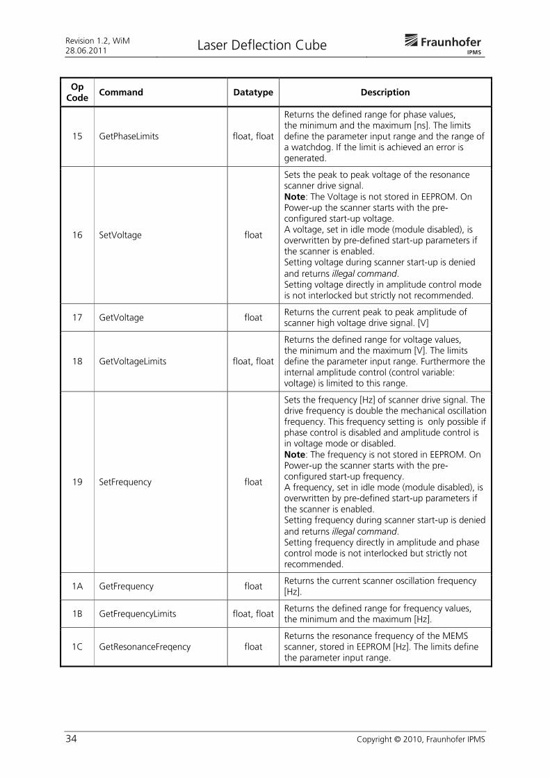
Op Code
Command Datatype Description
15 GetPhaseLimits float, float
Returns the defined range for phase values, the minimum and the maximum [ns]. The limits define the parameter input range and the range of a watchdog. If the limit is achieved an error is generated.
16 SetVoltage float
Sets the peak to peak voltage of the resonance scanner drive signal. Note: The Voltage is not stored in EEPROM. On Power-up the scanner starts with the pre-configured start-up voltage. A voltage, set in idle mode (module disabled), is overwritten by pre-defined start-up parameters if the scanner is enabled. Setting voltage during scanner start-up is denied and returns illegal command. Setting voltage directly in amplitude control mode is not interlocked but strictly not recommended.
17 GetVoltage float Returns the current peak to peak amplitude of scanner high voltage drive signal. [V]
18 GetVoltageLimits float, float
Returns the defined range for voltage values, the minimum and the maximum [V]. The limits define the parameter input range. Furthermore the internal amplitude control (control variable: voltage) is limited to this range.
19 SetFrequency float
Sets the frequency [Hz] of scanner drive signal. The drive frequency is double the mechanical oscillation frequency. This frequency setting is only possible if phase control is disabled and amplitude control is in voltage mode or disabled. Note: The frequency is not stored in EEPROM. On Power-up the scanner starts with the pre-configured start-up frequency. A frequency, set in idle mode (module disabled), is overwritten by pre-defined start-up parameters if the scanner is enabled. Setting frequency during scanner start-up is denied and returns illegal command. Setting frequency directly in amplitude and phase control mode is not interlocked but strictly not recommended.
1A GetFrequency float Returns the current scanner oscillation frequency [Hz].
1B GetFrequencyLimits float, float Returns the defined range for frequency values, the minimum and the maximum [Hz].
1C GetResonanceFreqency float Returns the resonance frequency of the MEMS scanner, stored in EEPROM [Hz]. The limits define the parameter input range.
Laser Deflection Cube Revision 1.2, WiM
28.06.2011
Copyright © 2011, Fraunhofer IPMS 35
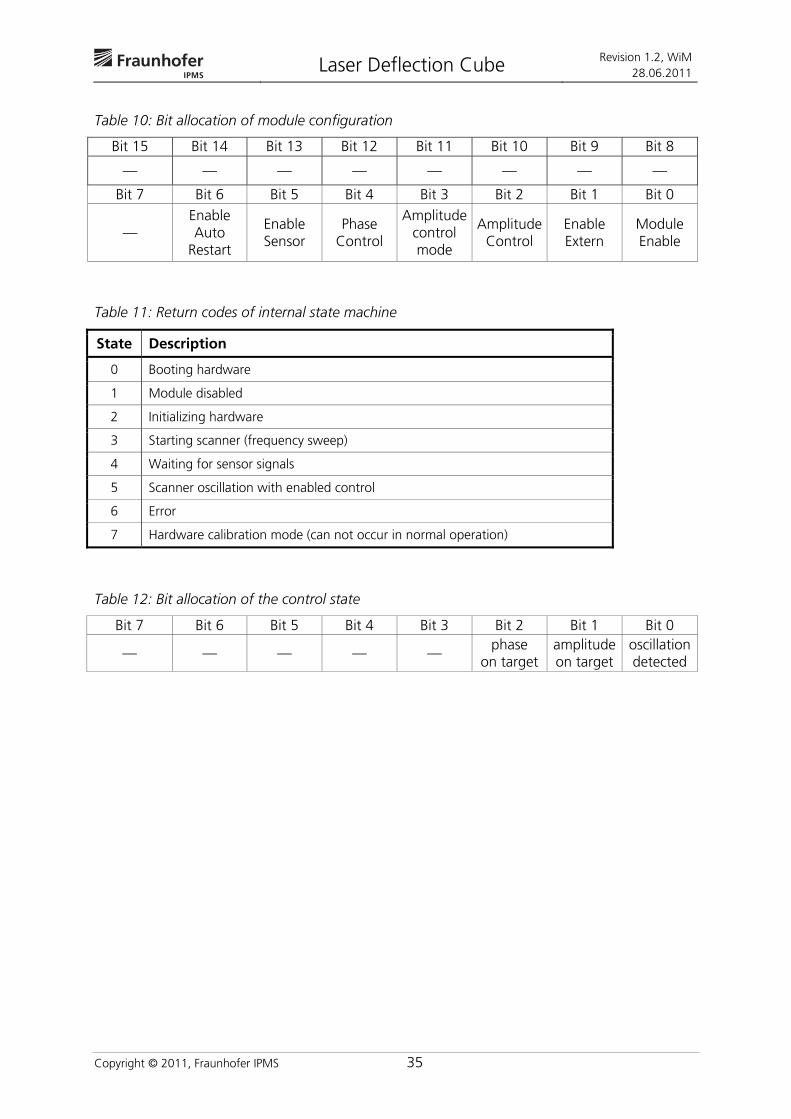
Table 10: Bit allocation of module configuration
Bit 15 Bit 14 Bit 13 Bit 12 Bit 11 Bit 10 Bit 9 Bit 8
— — — — — — — —
Bit 7 Bit 6 Bit 5 Bit 4 Bit 3 Bit 2 Bit 1 Bit 0
— Enable Auto
Restart
Enable Sensor
Phase Control
Amplitude control mode
AmplitudeControl
Enable Extern
Module Enable
Table 11: Return codes of internal state machine
State Description
0 Booting hardware
1 Module disabled
2 Initializing hardware
3 Starting scanner (frequency sweep)
4 Waiting for sensor signals
5 Scanner oscillation with enabled control
6 Error
7 Hardware calibration mode (can not occur in normal operation)
Table 12: Bit allocation of the control state
Bit 7 Bit 6 Bit 5 Bit 4 Bit 3 Bit 2 Bit 1 Bit 0
— — — — — phase
on target amplitude on target
oscillationdetected
Revision 1.2, WiM 28.06.2011 Laser Deflection Cube
36 Copyright © 2010, Fraunhofer IPMS
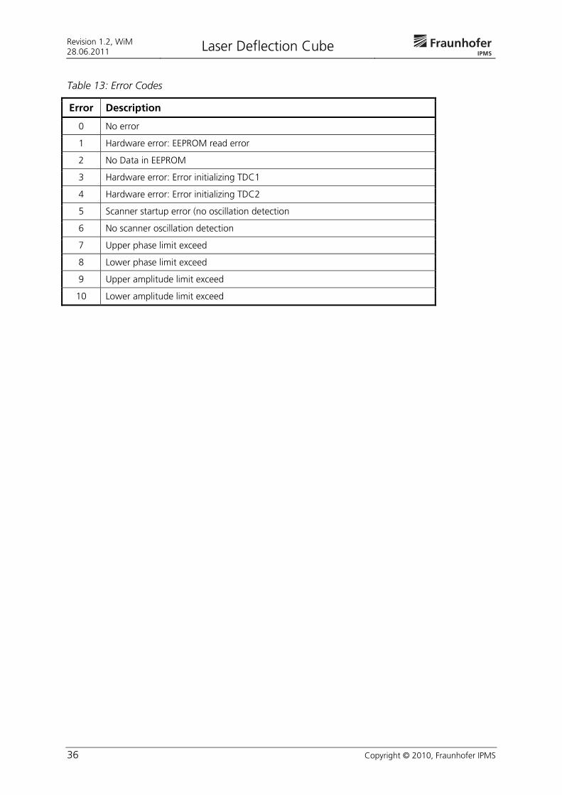
Table 13: Error Codes
Error Description
0 No error
1 Hardware error: EEPROM read error
2 No Data in EEPROM
3 Hardware error: Error initializing TDC1
4 Hardware error: Error initializing TDC2
5 Scanner startup error (no oscillation detection
6 No scanner oscillation detection
7 Upper phase limit exceed
8 Lower phase limit exceed
9 Upper amplitude limit exceed
10 Lower amplitude limit exceed

Laser Deflection Cube Revision 1.2, WiM
28.06.2011
Copyright © 2011, Fraunhofer IPMS 37
NOTES