latest development of mrf - epics
TRANSCRIPT

Micro-Research Finland Oy
Latest Development of MRF
Jukka Pietarinen
EPICS Collaboration MeetingHsinchu, June 16, 2011

Timing System Workbench (BNL)
Event receivers
Fan-out module
Event generator
Not shown: HP signal generator, a LeCroy WaveRunner Oscilloscope and a Transition module
IOC

New Event Generator Features(mrfioc2 beta release by Michael Davidsaver and Jayesh Shah)
• Runtime configurable• Software timestamp TX
–Frees 2 (of 8) inputs• Dynamic sequence
management–Store ready-to-run
sequences–Fast switching at
runtime• 10 events in ~30us

New Event Receiver Features(mrfioc2 beta release by Michael Davidsaver and Jayesh Shah)
• Only Base record types
• Complete runtime (re)configuration
• Same code for VME and PCI models
• Linux support• Support for event
uplink• New CML modes
http://epics.sourceforge.net/mrfioc2/

Micro-Research Finland Oy
[email protected] June 2011
cPCI-EVG-300 and cPCI-EVR-300• 6U form factor CompactPCI• Based on Lattice ECP3• Six Universal I/O slots• Redesign of cPCI-EVG-230 and cPCI-EVR-230 with same functionality and different form factor
(upgrade to more recent technology)

Micro-Research Finland Oy
[email protected] June 2011
Timestamping Improvements (for TPS)• Implement seconds logic in FPGA for automatic
timestamp event generation with an externally supplied 1 Hz clock
seconds counterExternal 1 Hz
increment
shift registerload
event code 0x7Dreset timestamp counter
event code 0x70 / 0x7132 bits of ‘0’/’1’

Micro-Research Finland Oy
[email protected] June 2011
New Gun Driver Set - cPCI-EVRTG-300• 6U form factor CompactPCI• Based on Virtex 5 FXT• Eight Outputs:
– GTX transceiver outputs– 40 x event clock resolution– Pulse/pattern outputs– Frequency generation– Two SFPs to drive GUN-RC– Two LVPECL outputs– Two Universal I/O slots
• four outpus of choice• GUN-TX inhibit input
– Low jitter– Delay fine tuning down to
~10 ps steps

Micro-Research Finland Oy
[email protected] June 2011
New Gun Driver Set - GUN-RC-300• Requirements:
– One channel– Arbitrary pulse patterns with
– Min. 1 ns pulses– Pulse to pulse spacing 2 ns
increments– Output level 3.3V TTL
• New modulation scheme– 200 ps resolution with GTX– > 5 gbps transceivers– Output stage challenging


Micro-Research Finland Oy
[email protected] June 2011
cRIO-EVR Universal I/O Carrier• Two Universal I/O slots
– four outputs/four inputs/two inputs & two outputs• USB port with UART
– serial communications interface to cRIO-EVR• Plugs into cRIO-EVR: stand-alone EVR with
– ethernet– two Universal I/O slots– serial port over USB
• How to control?– EPICS? (RTEMS port for lm32 exists)– etherCAT? (only one ethernet port)

Micro-Research Finland Oy
[email protected] June 2011
PCIe-EVR Requirements(designed for Diamond Light Source)
• PCIe form factor– standard height (max. 111.15 mm), half length
(max. 167.65 mm)• I/O on external rack mountable 1U Interface Module
– replaceable Universal I/O modules– indicator LEDs– differential low-voltage signals between PCIe-EVR
and Interface board over SCSI-5 cable• Compatibility with existing DLS timing system
(modular register map)

Micro-Research Finland Oy
[email protected] June 2011
PCIe-EVR Hardware Design• Based on cPCI-EVR-300 design
–PCI replaced with PCIe (Lattice IP core)–Lattice ECP3 FPGA–I/O on VHDCI
connector–SFP transceiver–two RGB LEDs–91.7 mm x 79.2 mm–14 layer PCB
Micro-Research Finland Oy
[email protected] June 2011
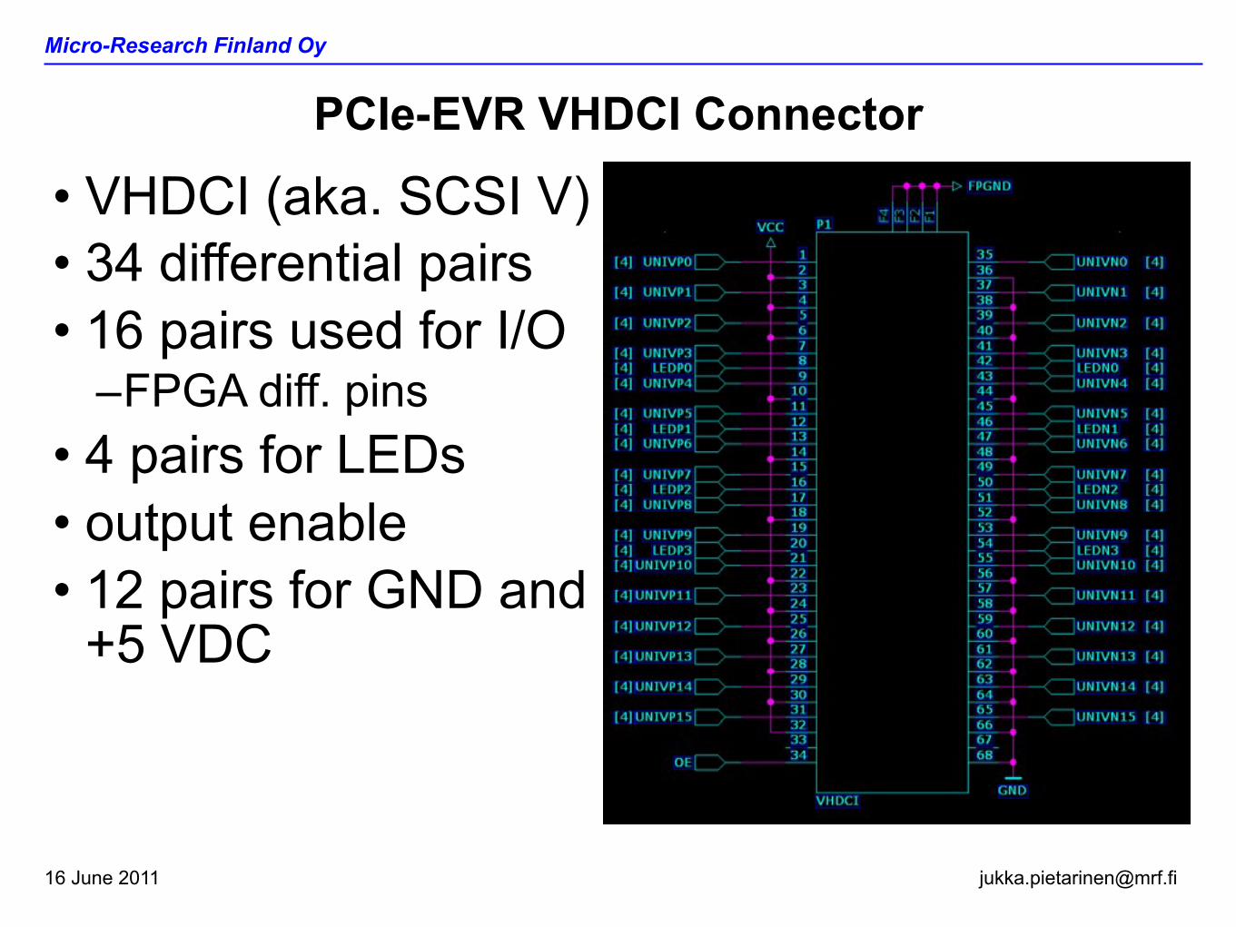
PCIe-EVR VHDCI Connector
• VHDCI (aka. SCSI V)• 34 differential pairs• 16 pairs used for I/O
–FPGA diff. pins• 4 pairs for LEDs• output enable• 12 pairs for GND and
+5 VDC

Micro-Research Finland Oy
[email protected] June 2011
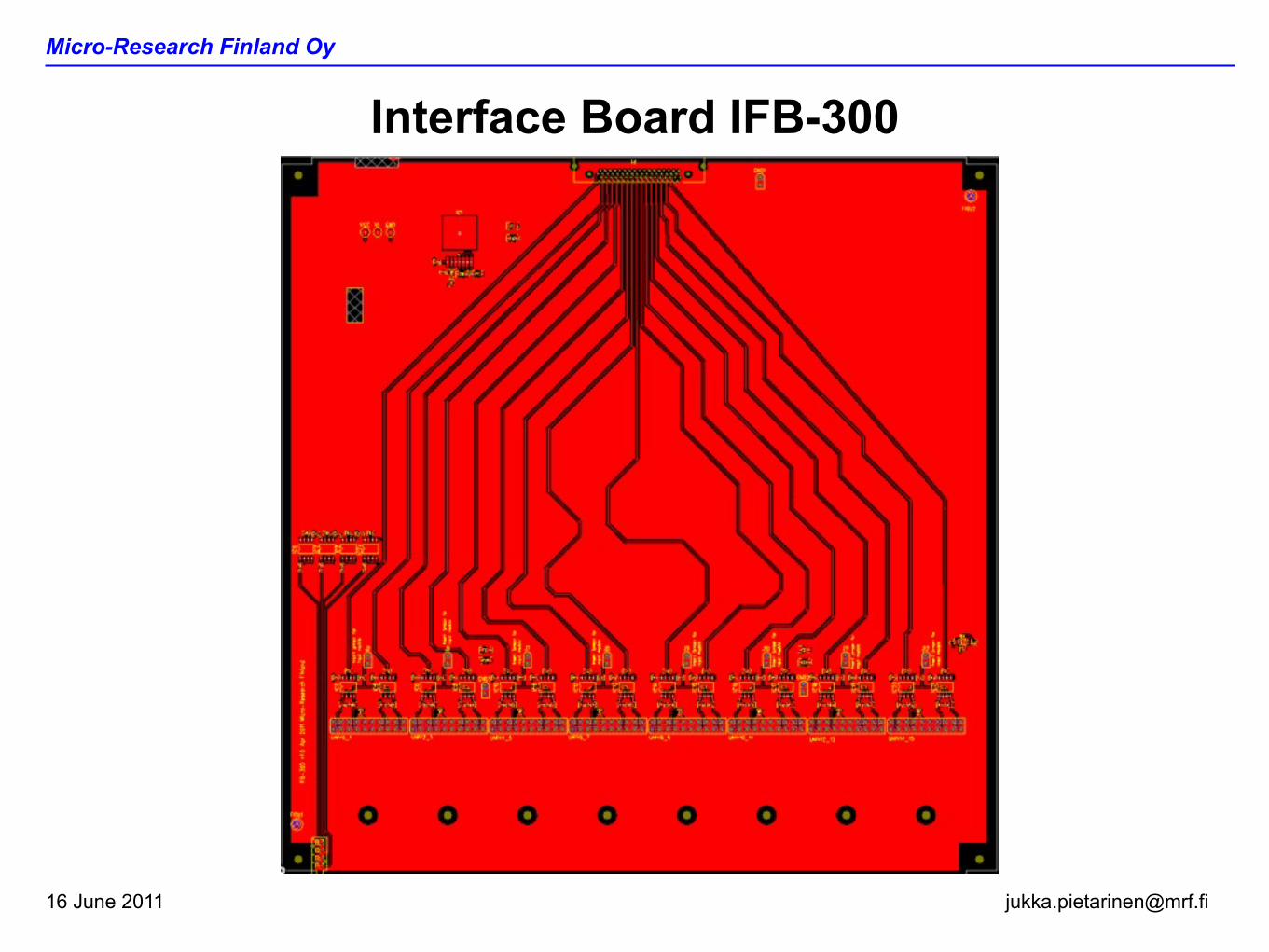
Interface Board IFB-300• Schroff 24572-100 ratiopacPRO case
–42.5 mm high, 255.5 mm deep–Holds one 6U PCB
• Eight Universal I/O slots• Four indicator LEDs

Micro-Research Finland Oy
[email protected] June 2011
Interface Board IFB-300
–Front side has a handle on the right hand side–To replace I/O modules one has to take off back
side VHDCI connector screws and loosen front panel fastening screws. PCB will slide out.

Micro-Research Finland Oy
[email protected] June 2011
Interface Board IFB-300• TI SN65MLVD206D M-LVDS transmitter and receiver
• Signal direction for Universal I/O slot is chosen with jumper (no jumper - output module, jumper mounted - input module)
1FEATURES APPLICATIONS
DESCRIPTION
4
3
1
2
DE
D
RE
R67
AB
LOGIC DIAGRAM (POSITIVE LOGIC)
5
4
2
3DE
D
RE
R1211
AB
109 Y
Z
SN65MLVD203, SN65MLVD207SN65MLVD201, SN65MLVD206
SN65MLVD201, SN65MLVD203SN65MLVD206, SN65MLVD207
SLLS558C–DECEMBER 2002–REVISED JANUARY 2007www.ti.com
MULTIPOINT-LVDS LINE DRIVER AND RECEIVER
• Low-Power High-Speed Short-Reach• Low-Voltage Differential 30- to 55- LineAlternative to TIA/EIA-485Drivers and Receivers for Signaling Rates(1)
• Backplane or Cabled Multipoint Data andUp to 200 MbpsClock Transmission• Type-1 Receivers Incorporate 25 mV of
• Cellular Base StationsHysteresis• Central-Office Switches• Type-2 Receivers Provide an Offset (100 mV)• Network Switches and RoutersThreshold to Detect Open-Circuit and Idle-Bus
Conditions• Meets or Exceeds the M-LVDS Standard
TIA/EIA-899 for Multipoint Data Interchange The SN65MLVD201, 203, 206, and 207 aremultipoint-low-voltage differential (M-LVDS) line• Controlled Driver Output Voltage Transitiondrivers and receivers, which are optimized to operateTimes for Improved Signal Qualityat signaling rates up to 200 Mbps. All parts comply
• -1 V to 3.4 V Common-Mode Voltage Range with the multipoint low-voltage differential signalingAllows Data Transfer With 2 V of Ground Noise (M-LVDS) standard TIA/EIA-899. These circuits are
similar to their TIA/EIA-644 standard compliant LVDS• Bus Pins High Impedance When Disabled orcounterparts, with added features to addressVCC 1.5 Vmultipoint applications. The driver output has been• 100-Mbps Devices Available (SN65MLVD200A, designed to support multipoint buses presenting202A, 204A, 205A) loads as low as 30 , and incorporates controlled
• M-LVDS Bus Power Up/Down Glitch Free transition times to allow for stubs off of the backbonetransmission line.The signaling rate of a line, is the number of voltage transitions
that are made per second expressed in the units bps (bits per These devices have Type-1 and Type-2 receiverssecond).that detect the bus state with as little as 50 mV ofdifferential input voltage over a common-modevoltage range of -1 V to 3.4 V. The Type-1 receiversexhibit 25 mV of differential input voltage hysteresisto prevent output oscillations with slowly changingsignals or loss of input. Type-2 receivers include anoffset threshold to provide a known output stateunder open-circuit, idle-bus, and other faultsconditions. The devices are characterized foroperation from –40°C to 85°C.
1
Please be aware that an important notice concerning availability, standard warranty, and use in critical applications ofTexas Instruments semiconductor products and disclaimers thereto appears at the end of this data sheet.
PRODUCTION DATA information is current as of publication date. Copyright © 2002–2007, Texas Instruments IncorporatedProducts conform to specifications per the terms of the TexasInstruments standard warranty. Production processing does notnecessarily include testing of all parameters.

Micro-Research Finland Oy
[email protected] June 2011
PCIe-EVR Current Status• Parts available in stock for prototype and production
batches• PCBs for prototypes in production (delivery date set
for June 7th)• Prototype (5 unit batch) PCB assembly immediately
when PCBs have arrived, assembly ready on week 24 (before June 17th).
• Mechanic parts (IFB cases, panels, PCIe bracket)have been ordered

Micro-Research Finland Oy
[email protected] June 2011
Future Plans - 10 MHz reference clock• A new Universal I/O module has been designed
(prototype in a few weeks):–with an Oscillator Frequency Upconverter–i.e. produce reference clock of 100 MHz or 125 MHz
with a reference input of 10 MHz (standard frequency of measurement equipment/PXI)
–mounted on EVG (VME-EVG-230/cPCI-EVG-230/cPCI-EVG-300) to allow using a lower frequency reference than 50 MHz - 125 MHz

Micro-Research Finland Oy
[email protected] June 2011
Future Plans - Requirements of SwissFEL• Sequencer changes
–multiple sequences with user defined playback order (similar to super sequencer)
• Higher event rate/bit rate 142.8 MHz (2.856 Gbit/s)• Increase precision of sequence trigger delay/phase
shifter• Another way of timestamping:
–multiplexed counter with fractional part that will allow for fine tuning of timestamp resolution
Micro-Research Finland Oy
[email protected] June 2011
Future Plans - Requirements of SwissFEL• Higher event rate/bit rate 142.8 MHz (2.856 Gbit/s)
–most challenging requirement–current CDRs go only up to 2.7 Gbit/s–omit CDRs in fan-outs?–regenerate event clock at fan-out
• will add delay of 100-200 ns fan-out level• lots of possibilities
–insert events
Micro-Research Finland Oy
[email protected] June 2011
Future Plans - Requirements of SwissFEL
• PSI preferred platform is VME–new VME-EVG?–new VME-EVR?–new Fan-Out for > 2.5 Gbit/s operation
• diagnostics• VME form factor?

Micro-Research Finland Oy
[email protected] June 2011
Future Plans - AMC?• An Event Receiver for microTCA / AMC
–PCIe on backplane (SLAC requirement)–GigE on backplane (KEK requirement)
• Could use same IFB-300 Interface Board as the PCIe-EVR
• Basically same design as PCIe-EVR-300 with the addition of IPMI management
Micro-Research Finland Oy
[email protected] June 2011
Future Plans - CompactPCI Express• An Event Receiver for the PXIe System Timing Slot
–100 MHz system reference clock PXIe_CLK100 in addition to conventional PXI 10 MHz
–three differential star triggers between each slot and the system timing module, two from STM to peripheral, one from peripheral to STM
• Could use same IFB-300 Interface Board as the PCIe-EVR

Micro-Research Finland Oy
[email protected] June 2011
Future Plans - What is most Importantor required first?
• AMC-EVR• new higher speed VME-EVG / VME-EVR / fan-out• new VME-ADC digitizer• PXIe-EVR