lcws04 - 20 apr 2004paul dauncey - calice readout1 calice ecal readout status paul dauncey for the...
Post on 22-Dec-2015
221 views
TRANSCRIPT
LCWS04 - 20 Apr 2004 Paul Dauncey - CALICE Readout 1
CALICE ECAL Readout Status
Paul Dauncey
For the CALICE-UK electronics group:A. Baird, D. Bowerman, P. Dauncey, C. Fry, R. Halsall, D. Mercer, M. Postranecky, M.Warren, O. Zorba
LCWS04 - 20 Apr 2004 Paul Dauncey - CALICE Readout 2
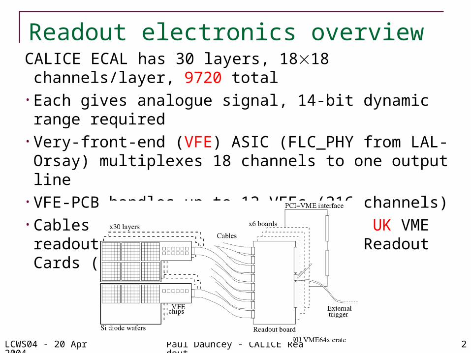
CALICE ECAL has 30 layers, 1818 channels/layer, 9720 total• Each gives analogue signal, 14-bit dynamic range required• Very-front-end (VFE) ASIC (FLC_PHY from LAL-Orsay)
multiplexes 18 channels to one output line• VFE-PCB handles up to 12 VFEs (216 channels)• Cables from VFE-PCBs go directly to UK VME readout boards,
called Calice Ecal Readout Cards (CERCs)
Readout electronics overview
LCWS04 - 20 Apr 2004 Paul Dauncey - CALICE Readout 3
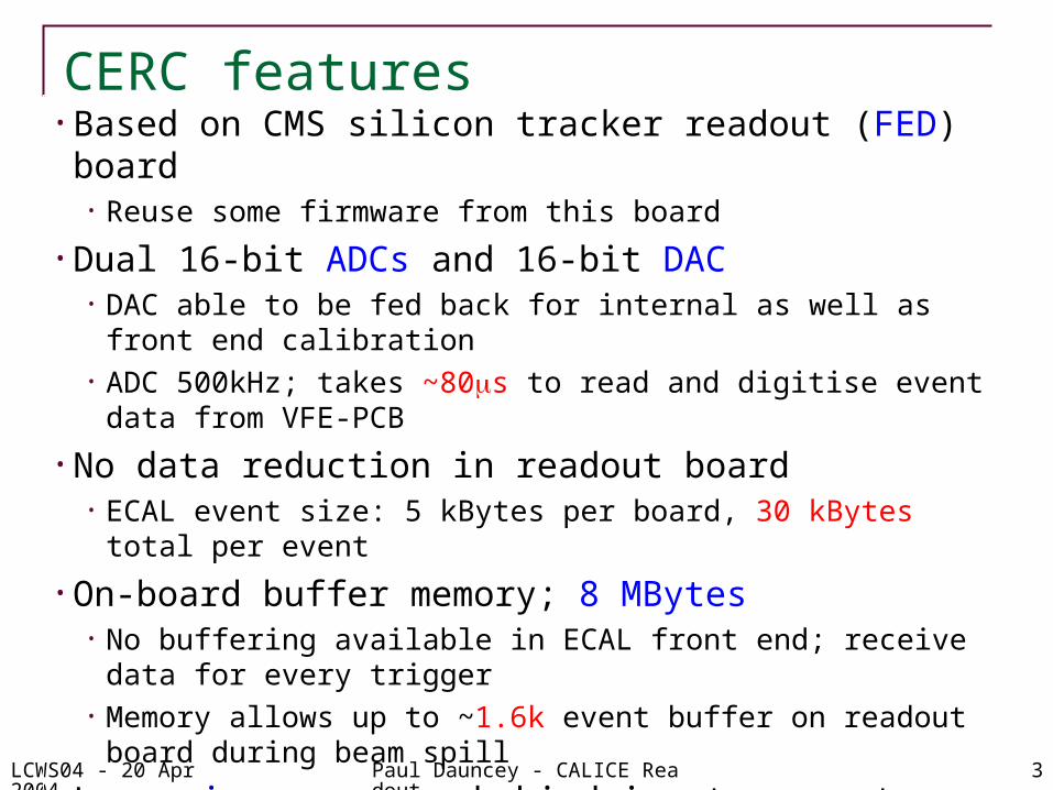
• Based on CMS silicon tracker readout (FED) board• Reuse some firmware from this board
• Dual 16-bit ADCs and 16-bit DAC• DAC able to be fed back for internal as well as front end calibration• ADC 500kHz; takes ~80s to read and digitise event data from VFE-PCB
• No data reduction in readout board• ECAL event size: 5 kBytes per board, 30 kBytes total per event
• On-board buffer memory; 8 MBytes• No buffering available in ECAL front end; receive data for every trigger• Memory allows up to ~1.6k event buffer on readout board during beam spill
• Large jumper array behind input connectors• Can select different signal I/O to and from connectors• Reroute signals to ADCs; one full or two half-full VFE-PCBs for each input• Bypass ADCs; purely digital I/O
CERC features
LCWS04 - 20 Apr 2004 Paul Dauncey - CALICE Readout 4
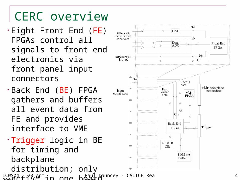
• Eight Front End (FE) FPGAs control all signals to front end electronics via front panel input connectors
• Back End (BE) FPGA gathers and buffers all event data from FE and provides interface to VME
• Trigger logic in BE for timing and backplane distribution; only active in one board
• Each input is one full or two half-full VFE-PCBs; need 45 inputs = 6 CERCs
CERC overview
LCWS04 - 20 Apr 2004 Paul Dauncey - CALICE Readout 5
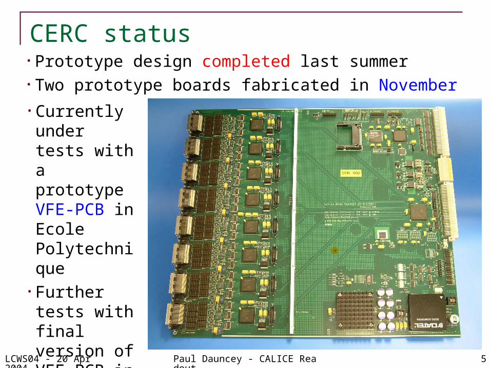
• Prototype design completed last summer• Two prototype boards fabricated in November
CERC status
• Currently under tests with a prototype VFE-PCB in Ecole Polytechnique
• Further tests with final version of VFE-PCB in May
• CERC final production in July
LCWS04 - 20 Apr 2004 Paul Dauncey - CALICE Readout 6
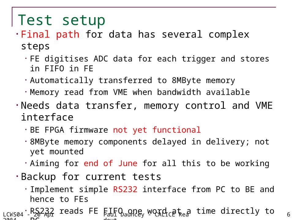
• Final path for data has several complex steps• FE digitises ADC data for each trigger and stores in FIFO in FE• Automatically transferred to 8MByte memory• Memory read from VME when bandwidth available
• Needs data transfer, memory control and VME interface• BE FPGA firmware not yet functional• 8MByte memory components delayed in delivery; not yet mounted• Aiming for end of June for all this to be working
• Backup for current tests• Implement simple RS232 interface from PC to BE and hence to FEs• RS232 reads FE FIFO one word at a time directly to PC• 8MByte memories bypassed, must read each event before next trigger• Rate is slow; ~1Hz of events, but sufficient for cosmics ~0.1Hz
• Analogue parts (ADC, DAC) operated as for final system• Noise, dynamic range, etc, measurements reliable
Test setup
LCWS04 - 20 Apr 2004 Paul Dauncey - CALICE Readout 7
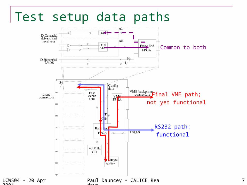
Test setup data paths
Common to both
Final VME path;
not yet functional
RS232 path;
functional
LCWS04 - 20 Apr 2004 Paul Dauncey - CALICE Readout 8
• RS232 path working• Read and write configuration data to RAMs in FEs• Read and write fake event to RAMs in FEs• Read back fake event via FIFO on trigger
• Trigger input working• Can fire trigger from BE with RS232 command• Can send trigger as LVDS signal on spare backplane pins to BE• Latter acts as external cosmic trigger path for VFE tests
• ADC readout and DAC control working• ADC can be read, DAC can be set• DAC can be looped back to ADC internally and through front panel• All VFE-PCB and ADC timing control software configurable• ADC data stored in FIFO and read through RS232
Firmware functional status
LCWS04 - 20 Apr 2004 Paul Dauncey - CALICE Readout 9
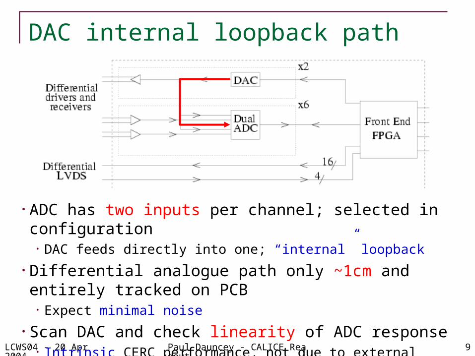
DAC internal loopback path
• ADC has two inputs per channel; selected in configuration• DAC feeds directly into one; “internal” loopback
• Differential analogue path only ~1cm and entirely tracked on PCB• Expect minimal noise
• Scan DAC and check linearity of ADC response• Intrinsic CERC performance, not due to external electronics, etc.
LCWS04 - 20 Apr 2004 Paul Dauncey - CALICE Readout 10
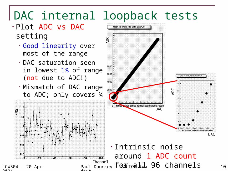
• Plot ADC vs DAC setting• Good linearity over most of the
range• DAC saturation seen in lowest
1% of range (not due to ADC!)• Mismatch of DAC range to
ADC; only covers ¼ of ADC range (0 to ~15k for ADC range of ±32k)
DAC internal loopback tests
• Intrinsic noise around 1 ADC count for all 96 channels
Channel
AD
C
AD
C
DAC
DAC
RM
S
LCWS04 - 20 Apr 2004 Paul Dauncey - CALICE Readout 11
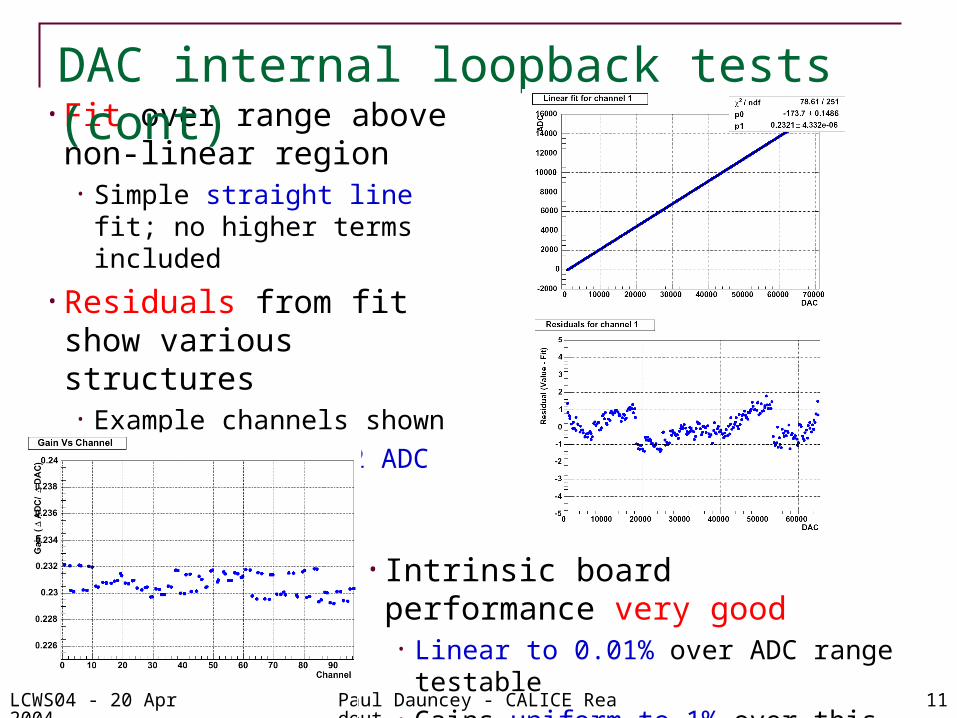
• Fit over range above non-linear region• Simple straight line fit; no higher
terms included
• Residuals from fit show various structures• Example channels shown• Typically under 2 ADC counts
DAC internal loopback tests (cont)
• Intrinsic board performance very good• Linear to 0.01% over ADC range testable• Gains uniform to 1% over this range
LCWS04 - 20 Apr 2004 Paul Dauncey - CALICE Readout 12
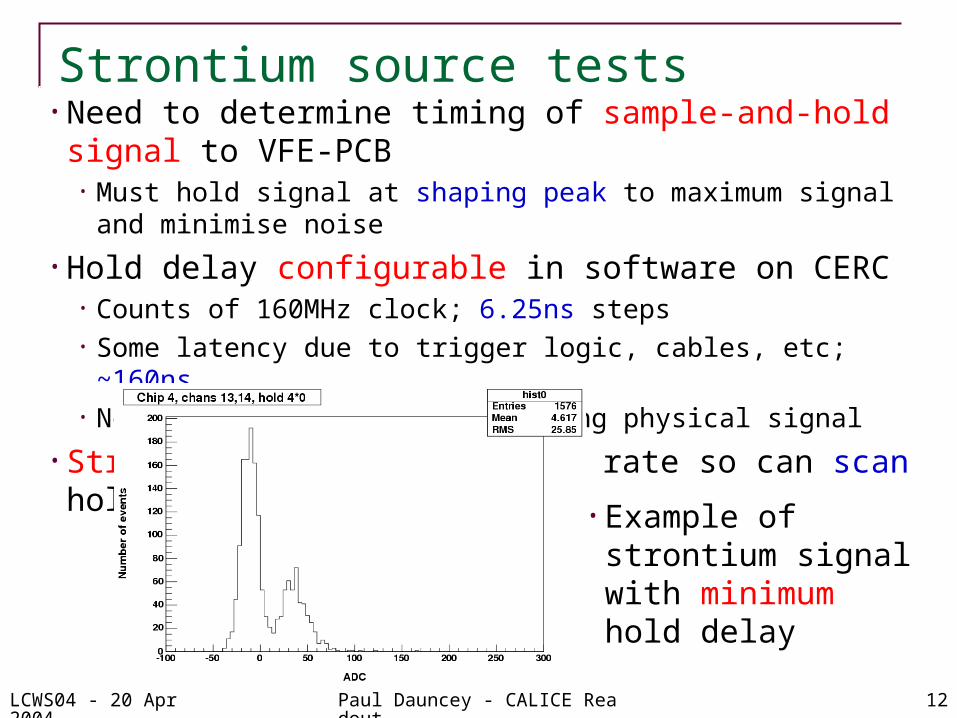
• Need to determine timing of sample-and-hold signal to VFE-PCB• Must hold signal at shaping peak to maximum signal and minimise noise
• Hold delay configurable in software on CERC• Counts of 160MHz clock; 6.25ns steps• Some latency due to trigger logic, cables, etc; ~160ns• Need to measure hold delay using physical signal
• Strontium beta source; high rate so can scan hold timing
Strontium source tests
• Example of strontium signal with minimum hold delay
LCWS04 - 20 Apr 2004 Paul Dauncey - CALICE Readout 13
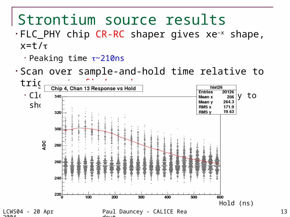
• FLC_PHY chip CR-RC shaper gives xe–x shape, x=t/• Peaking time ~210ns
• Scan over sample-and-hold time relative to trigger to find peak• Close to maximum allowable latency; will try to shorten trigger logic path!
Strontium source results
Hold (ns)
LCWS04 - 20 Apr 2004 Paul Dauncey - CALICE Readout 14
• Aim to provide absolute calibration using MIP peak• Check of full system dynamic range
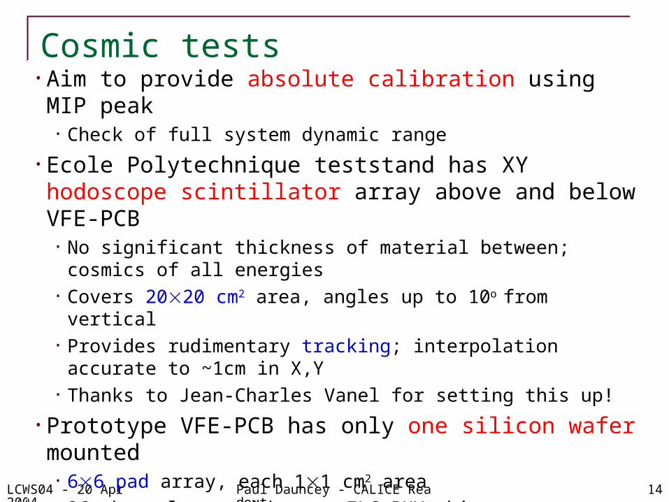
• Ecole Polytechnique teststand has XY hodoscope scintillator array above and below VFE-PCB• No significant thickness of material between; cosmics of all energies• Covers 2020 cm2 area, angles up to 10o from vertical• Provides rudimentary tracking; interpolation accurate to ~1cm in X,Y• Thanks to Jean-Charles Vanel for setting this up!
• Prototype VFE-PCB has only one silicon wafer mounted• 66 pad array, each 11 cm2 area• 36 channels, read by two FLC_PHY chips• Another two FLC_PHY chips mounted provide control comparison
• Active area is only ~10% of total teststand• Each silicon pad only hit once every ~360 triggers• Use hodoscope tracking to select events with cosmic close to wafer
Cosmic tests
LCWS04 - 20 Apr 2004 Paul Dauncey - CALICE Readout 15
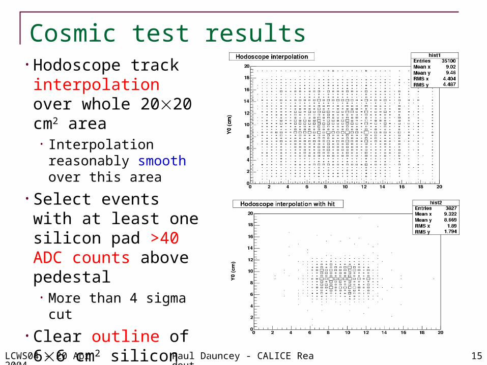
• Hodoscope track interpolation over whole 2020 cm2 area• Interpolation reasonably
smooth over this area
• Select events with at least one silicon pad >40 ADC counts above pedestal• More than 4 sigma cut
• Clear outline of 66 cm2 silicon wafer observed• Allows survey of position of
wafer• Pad-by-pad readout order
check also possible
Cosmic test results
LCWS04 - 20 Apr 2004 Paul Dauncey - CALICE Readout 16
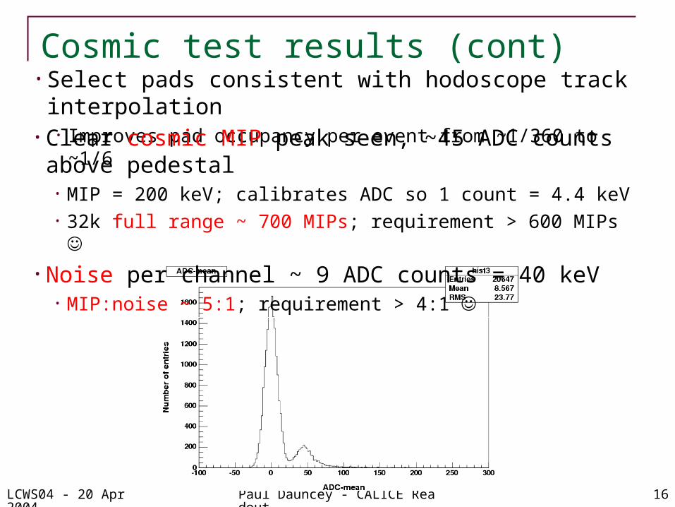
• Select pads consistent with hodoscope track interpolation• Improves pad occupancy per event from ~1/360 to ~1/6
Cosmic test results (cont)
• Clear cosmic MIP peak seen, ~45 ADC counts above pedestal• MIP = 200 keV; calibrates ADC so 1 count = 4.4 keV• 32k full range ~ 700 MIPs; requirement > 600 MIPs
• Noise per channel ~ 9 ADC counts = 40 keV• MIP:noise ~ 5:1; requirement > 4:1
LCWS04 - 20 Apr 2004 Paul Dauncey - CALICE Readout 17
• FPGAs do not always load correctly on CERC power-up• Thought to be due to power-up boot timing sequence
• Mismatch of DAC output op-amp differential range and ADC input op-amp differential range• DAC differential output only single polarity• Can only cover top half of ADC range• Incorrect resistor values used to set range; only half of the above range
• Common mode noise when coupled with VFE-PCB• Approximately half observed noise contribution
• Not yet clear if these can be fixed or require redesign• Risk in changing layout for production
BUT…• Prototype board has already demonstrated it meets requirements
for dynamic range, linearity and digital resolution
Known CERC problems
LCWS04 - 20 Apr 2004 Paul Dauncey - CALICE Readout 18
• CALICE also includes analogue and digital HCAL prototypes• AHCAL based on tile scintillator• Less stringent requirements (dynamic range, noise) than ECAL
• Potential to use CERC as readout board• AHCAL may also use ECAL FLC_PHY chip• Very similar readout so CERC directly usable in this case
• Large jumper array between input and FE FPGA• Firmware change allows large variety of I/O signals• Can mix analogue and digital as needed• Could even read out all-digital DHCAL
• Possibilities still under study• AHCAL would need ~6 more CERCs; still only one VME crate• DHCAL less clear, but could need ~20 CERCs; need two crates
Use for CALICE HCAL readout
LCWS04 - 20 Apr 2004 Paul Dauncey - CALICE Readout 19
• VFE-PCB tests in Paris continuing in May• Essential test of final VFE-PCB before moving to full production
• Possible AHCAL test at DESY in May/June• Prototype of AHCAL front end electronics fabricated by this time
• Finalise CERC redesign by end June• Decide if modifying prototype or not
• Relayout and fabricated nine production CERCs in July/August • Simple bricolage fix for known problems may be possible• If so, may not relayout; save a month
• ECAL system tests from September onwards• Initially at least 10 layers in cosmic teststand at Ecole Polytechnique• DESY ECAL electron beam test in Oct/Nov
• Beam tests with HCALs in hadron beams during 2005
Future plans