ldmos avionics radar transistor - stmicroelectronics is information on a product in full production....
TRANSCRIPT

This is information on a product in full production.
June 2015 DocID018767 Rev 7 1/14
STAC0912-250
LDMOS avionics radar transistor
Datasheet - production data
Figure 1. Pin connection
Features• Excellent thermal stability
• Common source configuration push-pull
• POUT = 250 W with 16 dB gain over 960 - 1215 MHz
• ST Air Cavity / STAC package
DescriptionThe STAC0912-250 is a common source N-channel enhancement-mode lateral field-effect RF power transistor designed for mode -S, T-CAS, JTIDS, DME or TACAN applications in the 960 to 1215 MHz frequency range.
STAC265BEpoxy sealed
1 - Drain
2 - Gate
3 - Source
1
2
3
Table 1. Device summary
Order code Package Branding
STAC0912-250 STAC265B 0912-250
www.st.com

Contents STAC0912-250
2/14 DocID018767 Rev 7
Contents
1 Electrical data . . . . . . . . . . . . . . . . . . . . . . . . . . . . . . . . . . . . . . . . . . . . . . 3
1.1 Maximum ratings . . . . . . . . . . . . . . . . . . . . . . . . . . . . . . . . . . . . . . . . . . . . 3
1.2 Thermal data . . . . . . . . . . . . . . . . . . . . . . . . . . . . . . . . . . . . . . . . . . . . . . . 3
2 Electrical characteristics . . . . . . . . . . . . . . . . . . . . . . . . . . . . . . . . . . . . . 4
2.1 Static . . . . . . . . . . . . . . . . . . . . . . . . . . . . . . . . . . . . . . . . . . . . . . . . . . . . . . 4
2.2 Dynamic . . . . . . . . . . . . . . . . . . . . . . . . . . . . . . . . . . . . . . . . . . . . . . . . . . . 4
3 Impedance data . . . . . . . . . . . . . . . . . . . . . . . . . . . . . . . . . . . . . . . . . . . . . 6
4 Typical performance . . . . . . . . . . . . . . . . . . . . . . . . . . . . . . . . . . . . . . . . . 7
5 Circuit and BOM . . . . . . . . . . . . . . . . . . . . . . . . . . . . . . . . . . . . . . . . . . . . 8
6 Package mechanical data . . . . . . . . . . . . . . . . . . . . . . . . . . . . . . . . . . . . 11
7 Revision history . . . . . . . . . . . . . . . . . . . . . . . . . . . . . . . . . . . . . . . . . . . 13

DocID018767 Rev 7 3/14
STAC0912-250 Electrical data
14
1 Electrical data
1.1 Maximum ratingsTCASE = 25 °C
1.2 Thermal data
Table 2. Absolute maximum ratings
Symbol Parameter Value Unit
V(BR)DSS Drain-source voltage 80 V
VGS Gate-source voltage ± 20 V
PDISS Power dissipation (@ TC = 70 °C) 928 W
TJ Max. operating junction temperature 200 °C
TSTG Storage temperature - 65 to + 150 °C
Table 3. Thermal data @ 100 µs - 10 %
Symbol Parameter Value Unit
RthJC Junction - case thermal resistance 0.14 °C/W
Electrical characteristics STAC0912-250
4/14 DocID018767 Rev 7
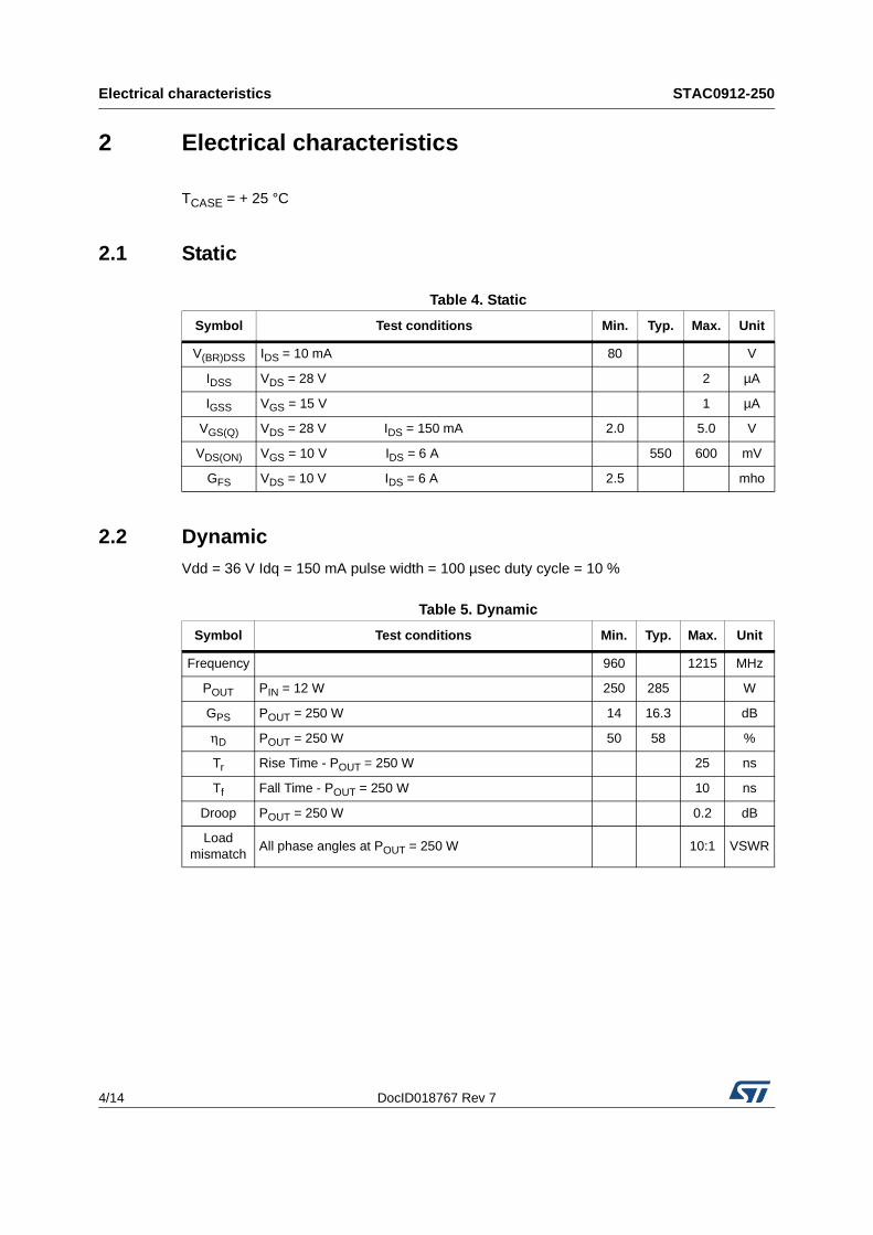
2 Electrical characteristics
TCASE = + 25 °C
2.1 Static
2.2 DynamicVdd = 36 V Idq = 150 mA pulse width = 100 µsec duty cycle = 10 %
Table 4. Static
Symbol Test conditions Min. Typ. Max. Unit
V(BR)DSS IDS = 10 mA 80 V
IDSS VDS = 28 V 2 µA
IGSS VGS = 15 V 1 µA
VGS(Q) VDS = 28 V IDS = 150 mA 2.0 5.0 V
VDS(ON) VGS = 10 V IDS = 6 A 550 600 mV
GFS VDS = 10 V IDS = 6 A 2.5 mho
Table 5. Dynamic
Symbol Test conditions Min. Typ. Max. Unit
Frequency 960 1215 MHz
POUT PIN = 12 W 250 285 W
GPS POUT = 250 W 14 16.3 dB
ηD POUT = 250 W 50 58 %
Tr Rise Time - POUT = 250 W 25 ns
Tf Fall Time - POUT = 250 W 10 ns
Droop POUT = 250 W 0.2 dB
Load mismatch
All phase angles at POUT = 250 W 10:1 VSWR

DocID018767 Rev 7 5/14
STAC0912-250 Electrical characteristics
14
Table 6. Reference data(1)
Mode of operation
Pulse conditions
VDD
(V)
POUT
(W)
Gain
(dB)
Delta gain
(dB)
Eff.
(%)
Pulse droop
(dB)
TR
(nsec)
TF
(nsec)
RTHJ-C
(°C/W)
All modes100µsec -
10%36 250 16 0.7 58 0.1 25 5 0.14
TCAS1030 - 1090
MHz32µsec - 1% 36 250 16 0.3 57 0.1 25 5 0.06
Mode-S
1030 - 1090 MHz
128µsec - 2% 36 250 15.5 0.3 56 0.2 25 5 0.125
340µsec - 1% 36 250 15.5 0.3 56 0.25 25 5 0.17
1. Typical RF performance measured in common source class-AB broadband circuit 960 MHz to 1215 MHz frequency band. Th = 25 °C; RTHJ-C = 0.15°C/W; unless specified otherwise.
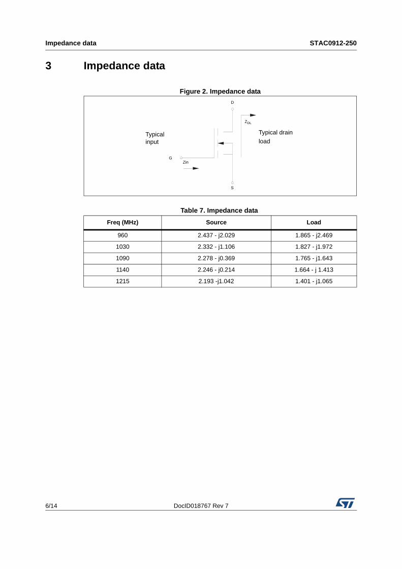
Impedance data STAC0912-250
6/14 DocID018767 Rev 7
3 Impedance data
Figure 2. Impedance data
Table 7. Impedance data
Freq (MHz) Source Load
960 2.437 - j2.029 1.865 - j2.469
1030 2.332 - j1.106 1.827 - j1.972
1090 2.278 - j0.369 1.765 - j1.643
1140 2.246 - j0.214 1.664 - j 1.413
1215 2.193 -j1.042 1.401 - j1.065
Typical drain
load Typical input
GZin
ZDL
D
S

DocID018767 Rev 7 7/14
STAC0912-250 Typical performance
14
4 Typical performance
Figure 3. Gain vs. output power Figure 4. Efficiency vs output power
Figure 5. Output power and efficiency vs frequency
10
11
12
13
14
15
16
17
18
19
20
0 25 50 75 100 125 150 175 200 225 250 275 300 325 350
Gai
n -dB
-
Output Power -Watt-
960MHz 1030MHz 1090MHz 1140MHz 1215MHz
Vdd=36Volt-Idq=150mAPw=100us- DC=10%
AM10120V1
0
10
20
30
40
50
60
70
0 25 50 75 100 125 150 175 200 225 250 275 300 325 350
Effic
einc
y %
Output Power - Watt-
960MHz 1300MHz 1090MHz 1140MHz 1215MHz
Vdd=36Volt-Idq=150mAPw=100us- DC=10%
AM10121V1
20
25
30
35
40
45
50
55
60
65
70
250
260
270
280
290
300
310
320
330
340
350
940 990 1040 1090 1140 1190
Effici
ency
%
Pout
-Wa�
-
Frequency - MHz-
Pout-15W in- Pout-12W in- Efficiency-12W in- Efficiency-15W in-
Vdd=36Volt-Idq=150mAPw=100us - DC=10%
AM10122V1

Circuit and BOM STAC0912-250
8/14 DocID018767 Rev 7
5 Circuit and BOM
Figure 6. Broadband 960-1215 MHz circuit

DocID018767 Rev 7 9/14
STAC0912-250 Circuit and BOM
14
Table 8. Components list
Item Qty Part NO Vendor Description, dimension (x,y)
C1, C16,C17,C18
4 1111C360G501X Passive Plus Inc. 36pF chip ceramic capacitor
C2 1 1111C2R2G501X Passive Plus Inc. 2.2pF chip ceramic capacitor
C3 1 1111C3R0G501X Passive Plus Inc. 3.0pF chip ceramic capacitor
C4,C5 2 1111C5R6G501X Passive Plus Inc. 5.6pF chip ceramic capacitor
C6,C9 2 1111C1R4G501X Passive Plus Inc. 1.4pF chip ceramic capacitor
C7,C10 2 1111C3R9G501X Passive Plus Inc. 3.9pF chip ceramic capacitor
C8,C11 2 1111C4R7G501X Passive Plus Inc. 4.7pF chip ceramic capacitor
C12,C13 2 1111C1R7G501X Passive Plus Inc. 1.7pF chip ceramic capacitor
C14,C15 2 1111C1R6G501X Passive Plus Inc. 1.6pF chip ceramic capacitor
C19 1 UPW1E331MPD Nichicon 230µF, 25V electrolytic capacitor
C20 1 TVX1J102MCD Nichicon 1000µF, 63V electrolytic capacitor
C21 1 TVA1346 Vishay Sprague 100µF, 100V electrolytic capacitor
R1 1 CR1206-4W-681JB Venkel 390 Ohm surface mount resistor
R2 1 CR1206-4W-821JB Venkel 820 Ohm surface mount resistor
L1 1 1606-9G Coil Craft 9.85nH air core inductor
T1 L= 0.278in W=0.082in
T2 L= 0.134in W=0.082in
T3 L= 0.736in W=0.748in
T4 L= 0.674in W=0.748in
T5 L= 0.100in W=0.082in
T6 L= 0.365in W=0.082in
T7 L= 1.160in W=0.082in
Board 3X5 1 Rogers Corp 0.030 THK, Er=2.5, 2Oz Cu both sides

Circuit and BOM STAC0912-250
10/14 DocID018767 Rev 7
Figure 7. Photo of the demonstration board

DocID018767 Rev 7 11/14
STAC0912-250 Package mechanical data
14
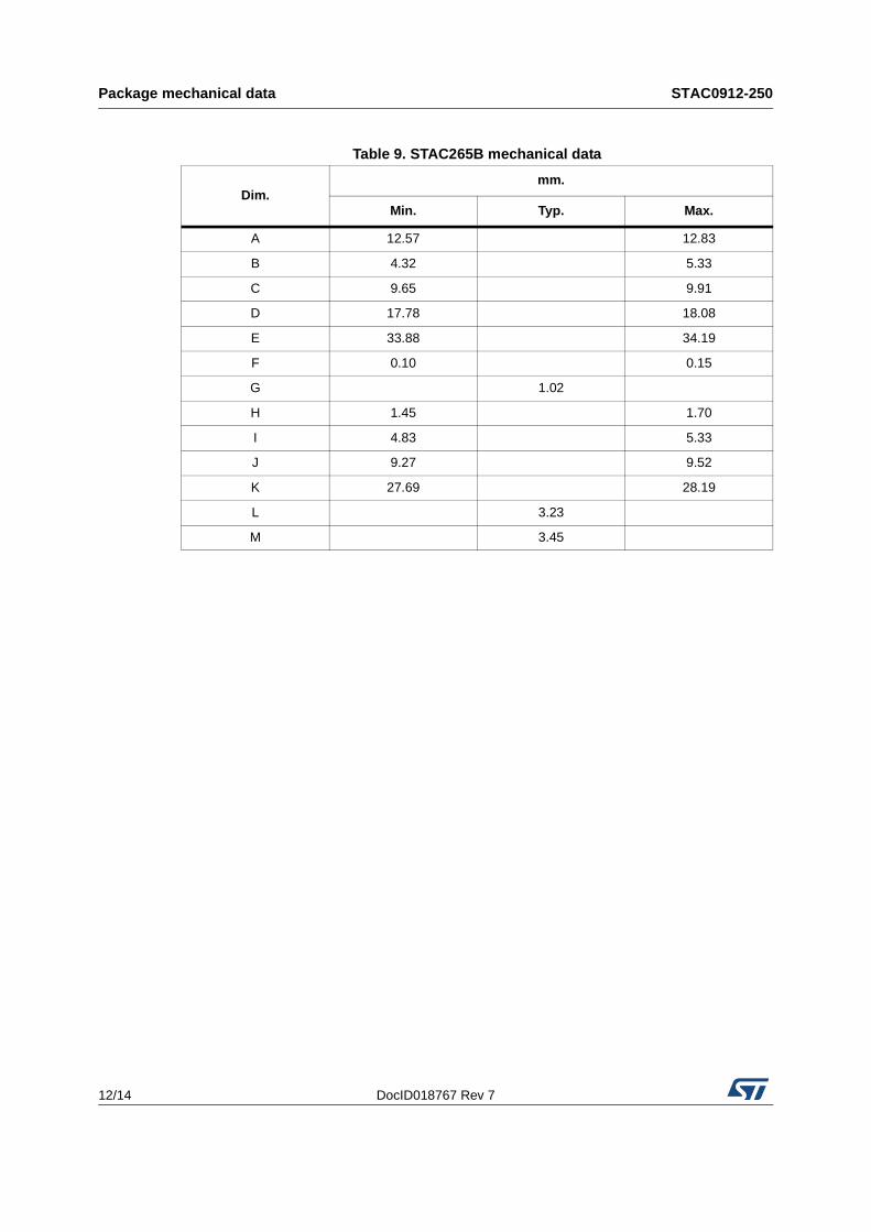
6 Package mechanical data
In order to meet environmental requirements, ST offers these devices in different grades of ECOPACK® packages, depending on their level of environmental compliance. ECOPACK® specifications, grade definitions and product status are available at: www.st.com. ECOPACK® is an ST trademark.
Figure 8. Package dimensions
Package mechanical data STAC0912-250
12/14 DocID018767 Rev 7
Table 9. STAC265B mechanical data
Dim.mm.
Min. Typ. Max.
A 12.57 12.83
B 4.32 5.33
C 9.65 9.91
D 17.78 18.08
E 33.88 34.19
F 0.10 0.15
G 1.02
H 1.45 1.70
I 4.83 5.33
J 9.27 9.52
K 27.69 28.19
L 3.23
M 3.45

DocID018767 Rev 7 13/14
STAC0912-250 Revision history
14
7 Revision history
Table 10. Document revision history
Date Revision Changes
20-Apr-2011 1 First release.
09-Aug-2011 2
– Updated features on cover page.– Updated PDISS value in Table 2: Absolute maximum ratings, RthJC
value in Table 3: Thermal data @ 100 µs - 10 %.– Updated typical and maximum values in Table 5: Dynamic– Inserted new Table 6: Reference data and Section 3: Impedance
data.– Updated figures: 3, 4 and 5.
– Minor text changes.
13-Sep-2011 3 Added Section 5: Circuit and BOM.
06-Jun-2012 4– Modified: Figure 6– Added: Figure 7
– Updated the entire Table 8
24-Sep-2012 5Updated title on the cover page.
Updated Table 4.
15-May-2014 6
Updated Figure 8: Package dimensions.
Minor text changes.Document status promoted from preliminary to production data.
11-Jun-2015 7Updated Section 3: Impedance data, Section 4: Typical performance and Section 5: Circuit and BOM.

STAC0912-250
14/14 DocID018767 Rev 7
IMPORTANT NOTICE – PLEASE READ CAREFULLY
STMicroelectronics NV and its subsidiaries (“ST”) reserve the right to make changes, corrections, enhancements, modifications, and improvements to ST products and/or to this document at any time without notice. Purchasers should obtain the latest relevant information on ST products before placing orders. ST products are sold pursuant to ST’s terms and conditions of sale in place at the time of order acknowledgement.
Purchasers are solely responsible for the choice, selection, and use of ST products and ST assumes no liability for application assistance or the design of Purchasers’ products.
No license, express or implied, to any intellectual property right is granted by ST herein.
Resale of ST products with provisions different from the information set forth herein shall void any warranty granted by ST for such product.
ST and the ST logo are trademarks of ST. All other product or service names are the property of their respective owners.
Information in this document supersedes and replaces information previously supplied in any prior versions of this document.
© 2015 STMicroelectronics – All rights reserved