le roux badenhorst - rochester institute of technologyridl.cfd.rit.edu/products/cryogenic...
TRANSCRIPT
UNIVERS ITE IT •STELLENBOSCH •UNIVERS ITY
j ou kenn i s v ennoo t • you r know ledge pa r tne r
Cryogenic Amplifiers for InterfacingSuperconductive Systems to Room
Temperature Electronics
by
Le Roux Badenhorst
Thesis presentedin partial fulfilment of the requirements for the degree of
Master of Science in Engineering(Electronic Engineering)
at the
University of Stellenbosch
Department of Electrical and Electronic Engineering,University of Stellenbosch,
Private Bag X1, 7602 Matieland, South Africa.
Supervisor: Dr CJ Fourie
December 2008
Declaration
By submitting this thesis electronically, I declare that the entirety of the workis my own, original work, that I am the owner of the copyright thereof (unlessto the extent explicitly otherwise stated) and that I have not previously in itsentirety or in part submitted it for obtaining any qualification.
Copyright © 2008 University of StellenboschAll rights reserved.
Abstract
This thesis is aimed at testing commercially available CMOS amplifier ICs at
4 K. Super Conducting Electronics (SCE) will also be used to amplify RSFQ
signals for easier detection by CMOS technology and better signal-to-noise
ratios.
The SCE comprises of a Suzuki stack amplifier, a 250 µA JTL and a
DC-to-SFQ converter. The Suzuki stack amplifier is simulated in WRSPICE.
It is able to amplify an SFQ signal synchronised with an external clock signal.
The amplified signal can then be detected by a normal commercially available
CMOS amplifier IC.
To keep the noise in the signal to a minimum, the commercial amplifier must
be be situated as close as possible to the SCE. The amplifier must therefore
be able to operate at 4 K. Ten different amplifier ICs were tested and three
was found that worked down to 4 K.
ii
Opsomming
Hierdie tesis is gemik op die toets van komersieel beskikbare CMOS versterker
geıntegreerde stroombane by 4 K. Supergeleier elektronika (SGE) gaan ook
gebruik word om RSFQ seine te versterk, sodat dit makliker deur CMOS
tegnologie bespeur kan word en ’n beter sein-tot-ruis verhouding kan he.
Die SGE bestaan uit ’n Suzuki stapel versterker, ’n 250 µA JTL en ’n
DC-na-SFQ omskakelaar. Die Suzuki stapel versterker was slegs gesimuleer in
WRSPICE. Dit kan ’n SFQ sein versterk en dit sinchroniseer met ’n eksterne
klok sein. Die versterkte sein kan dan makliker deur normale komersieel
beskikbare CMOS versterkers bespeur word.
Om die ruis van die sein minimaal te hou, moet die komersiele versterkers so
na as moontlik aan die SGE wees. Daarom moet die versterker by 4 K kan
werk. Tien verskillende versterkers was getoets, waarvan drie kon werk tot by
4 K.
iii
Acknowledgement
I would like to thank:
• The Department of Electrical and Electronic Engineering of the
University of Stellenbosch for the use of the resources and equipment
required to complete this thesis.
• Dr C J Fourie for his guidance as supervisor.
• CES (Central Electronic Services), specifically Mr. U. Buttner for his
help.
• Mr. A. Cupido for creating the PCB designs used in this thesis.
• My fellow colleagues for being so supportive and available to exchange
problems and ideas
• Ma en Pa vir julle motivering en al julle gebede wat my gedra het.
iv
Contents
Declaration i
Abstract ii
Opsomming iii
Acknowledgement iv
Contents v
List of Figures vii
List of Tables x
Nomenclature xi
1 Introduction 11.1 Background . . . . . . . . . . . . . . . . . . . . . . . . . . . . 11.2 Research Objectives . . . . . . . . . . . . . . . . . . . . . . . . 31.3 Thesis Overview . . . . . . . . . . . . . . . . . . . . . . . . . . 3
2 Background and Specifications 42.1 Josephson Junctions . . . . . . . . . . . . . . . . . . . . . . . 42.2 SQUID Devices . . . . . . . . . . . . . . . . . . . . . . . . . . 52.3 RSFQ Signals . . . . . . . . . . . . . . . . . . . . . . . . . . . 62.4 Low Temperature Measurements . . . . . . . . . . . . . . . . . 82.5 Cryorefrigerator . . . . . . . . . . . . . . . . . . . . . . . . . . 92.6 Suzuki Stack Amplifier . . . . . . . . . . . . . . . . . . . . . . 112.7 DC SQUID Amplifier . . . . . . . . . . . . . . . . . . . . . . . 152.8 CMOS Amplifiers . . . . . . . . . . . . . . . . . . . . . . . . . 17
2.8.1 350 nm Channel Length or Smaller . . . . . . . . . . . 212.8.2 Hi-CMOS Technology . . . . . . . . . . . . . . . . . . 232.8.3 p-HEMT . . . . . . . . . . . . . . . . . . . . . . . . . . 24
2.9 Cryogenic behaviour of resistors and capacitors . . . . . . . . 26
v
CONTENTS vi
3 Design Overview 283.1 SCE Design Considerations . . . . . . . . . . . . . . . . . . . 28
3.1.1 SCE Block Diagram . . . . . . . . . . . . . . . . . . . 293.1.2 DC-to-SFQ Converter Circuit Layout . . . . . . . . . . 323.1.3 JTL250 Circuit Layout . . . . . . . . . . . . . . . . . . 343.1.4 Current Block . . . . . . . . . . . . . . . . . . . . . . . 353.1.5 Suzuki Stack Amplifier Circuit Layout . . . . . . . . . 363.1.6 Monte Carlo Analysis . . . . . . . . . . . . . . . . . . . 423.1.7 SCE Layout . . . . . . . . . . . . . . . . . . . . . . . . 45
3.2 Cryogenic Measurements Block Diagram . . . . . . . . . . . . 493.2.1 Cryogenic Measurements Setup . . . . . . . . . . . . . 50
4 Measurements and Results 554.1 Suzuki Stack Amplifier . . . . . . . . . . . . . . . . . . . . . . 554.2 Commercially Available Amplifiers . . . . . . . . . . . . . . . 56
4.2.1 HMC548 SiGe HBT Amplifier . . . . . . . . . . . . . . 584.2.2 HMC460 GaAs p-HEMT Low Noise Amplifier . . . . . 604.2.3 THS4304 SiGe BiCom-III Operational Amplifier . . . . 68
4.3 Summary . . . . . . . . . . . . . . . . . . . . . . . . . . . . . 72
5 Conclusions and Future Work 745.1 Research Findings . . . . . . . . . . . . . . . . . . . . . . . . . 74
5.1.1 Superconducting Electronics . . . . . . . . . . . . . . . 745.1.2 Commercially Available Amplifiers . . . . . . . . . . . 75
5.2 Improvements and Future Work . . . . . . . . . . . . . . . . . 77
Bibliography 78
List of Figures
2.1 Circuit layout of a DC-SQUID. . . . . . . . . . . . . . . . . . . 62.2 Amplitude against time graph of a single SFQ pulse . . . . . . . 72.3 Illustration of a Cryo Dipstick. . . . . . . . . . . . . . . . . . . . 92.4 Representation of the Cryomech PT405 cryocooler . . . . . . . 102.5 Basic configuration of a Suzuki stack amplifier . . . . . . . . . . 122.6 Current against time graph in a Suzuki stack amplifier. . . . . . 132.7 Voltage against time graph in a Suzuki stack amplifier. . . . . . 132.8 Basic configuration of a two-stage SQUID amplifier circuit. . . . 162.9 Subthreshold current characteristics as cited in [1]. . . . . . . . 182.10 Cross section of a CMOS transistor pair as cited in [1]. . . . . . 192.11 Variations of sheet resistances for polysilicon, p+-, and n+-type
diffusion layers, as well as p-Well and Al metals with decreasingtemperature as measured by [1]. . . . . . . . . . . . . . . . . . 20
2.12 Latch-up base current versus temperature . . . . . . . . . . . . 212.13 Dependence of the propagation delay of a CMOS inverter
fabricated by a 0.35 µm CMOS process on the supply voltageat 300 K and 4 K [2]. . . . . . . . . . . . . . . . . . . . . . . . . 22
2.14 Cross section of a AlGaAs/GaAs p-HEMT . . . . . . . . . . . . 252.15 Tested resistor types with characteristic plots against cryogenic
temperature range . . . . . . . . . . . . . . . . . . . . . . . . . 262.16 Tested capacitor types with characteristic plots against cryogenic
temperature range . . . . . . . . . . . . . . . . . . . . . . . . . 27
3.1 Block diagram of the SCE. . . . . . . . . . . . . . . . . . . . . . 303.2 Full circuit layout of the SCE. . . . . . . . . . . . . . . . . . . . 313.3 Circuit layout of the DC-to-SFQ converter. . . . . . . . . . . . . 323.4 Time analysis of the input and output signals of the DC-to-SFQ
converter. . . . . . . . . . . . . . . . . . . . . . . . . . . . . . . 343.5 Circuit layout of the JTL250. . . . . . . . . . . . . . . . . . . . 343.6 Time analysis of the input and output signals of the 250 µA JTL. 353.7 Time analysis of the voltage through the current block. . . . . . 363.8 Circuit layout of the Suzuki stack amplifier. . . . . . . . . . . . 37
vii
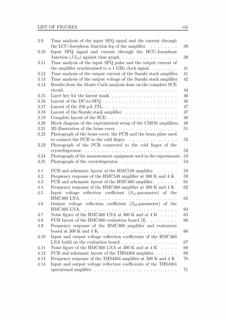
LIST OF FIGURES viii
3.9 Time analysis of the input SFQ signal and the current throughthe LCC-Josephson Junction leg of the amplifier. . . . . . . . . 39
3.10 Input SFQ signal and current through the HCC-JosephsonJunction (JJ12) against time graph. . . . . . . . . . . . . . . . . 39
3.11 Time analysis of the input SFQ pulse and the output current ofthe amplifier synchronised to a 1 GHz clock signal. . . . . . . . 41
3.12 Time analysis of the output current of the Suzuki stack amplifier. 413.13 Time analysis of the output voltage of the Suzuki stack amplifier. 423.14 Results from the Monte Carlo analysis done on the complete SCE
circuit. . . . . . . . . . . . . . . . . . . . . . . . . . . . . . . . . 443.15 Layer key for the layout mask. . . . . . . . . . . . . . . . . . . . 463.16 Layout of the DC-to-SFQ. . . . . . . . . . . . . . . . . . . . . . 463.17 Layout of the 250 µA JTL. . . . . . . . . . . . . . . . . . . . . . 473.18 Layout of the Suzuki stack amplifier. . . . . . . . . . . . . . . . 473.19 Complete layout of the SCE. . . . . . . . . . . . . . . . . . . . . 483.20 Block diagram of the experimental setup of the CMOS amplifiers. 493.21 3D illustration of the brass cover. . . . . . . . . . . . . . . . . . 513.22 Photograph of the brass cover, the PCB and the brass plate used
to connect the PCB to the cold finger. . . . . . . . . . . . . . . 523.23 Photograph of the PCB connected to the cold finger of the
cryorefrigerator. . . . . . . . . . . . . . . . . . . . . . . . . . . . 523.24 Photograph of the measurement equipment used in the experiments. 533.25 Photograph of the cryorefrigerator. . . . . . . . . . . . . . . . . 54
4.1 PCB and schematic layout of the HMC548 amplifier. . . . . . . 594.2 Frequency response of the HMC548 amplifier at 300 K and 4 K 594.3 PCB and schematic layout of the HMC460 amplifier. . . . . . . 614.4 Frequency response of the HMC460 amplifier at 300 K and 4 K 624.5 Input voltage reflection coefficient (S11-parameter) of the
HMC460 LNA. . . . . . . . . . . . . . . . . . . . . . . . . . . . 624.6 Output voltage reflection coefficient (S22-parameter) of the
HMC460 LNA. . . . . . . . . . . . . . . . . . . . . . . . . . . . 634.7 Noise figure of the HMC460 LNA at 300 K and at 4 K . . . . . 654.8 PCB layout of the HMC460 evaluation board [3]. . . . . . . . . 664.9 Frequency response of the HMC460 amplifier and evaluation
board at 300 K and 4 K. . . . . . . . . . . . . . . . . . . . . . . 664.10 Input and output voltage reflection coefficients of the HMC460
LNA build on the evaluation board. . . . . . . . . . . . . . . . . 674.11 Noise figure of the HMC460 LNA at 300 K and at 4 K . . . . . 684.12 PCB and schematic layout of the THS4304 amplifier. . . . . . . 694.13 Frequency response of the THS4304 amplifier at 300 K and 4 K 704.14 Input and output voltage reflection coefficients of the THS4304
operational amplifier. . . . . . . . . . . . . . . . . . . . . . . . . 71
LIST OF FIGURES ix
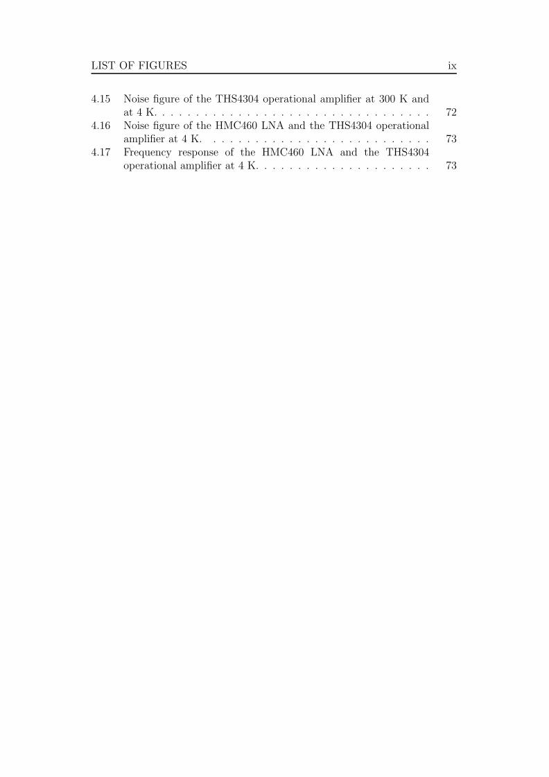
4.15 Noise figure of the THS4304 operational amplifier at 300 K andat 4 K. . . . . . . . . . . . . . . . . . . . . . . . . . . . . . . . . 72
4.16 Noise figure of the HMC460 LNA and the THS4304 operationalamplifier at 4 K. . . . . . . . . . . . . . . . . . . . . . . . . . . 73
4.17 Frequency response of the HMC460 LNA and the THS4304operational amplifier at 4 K. . . . . . . . . . . . . . . . . . . . . 73
List of Tables
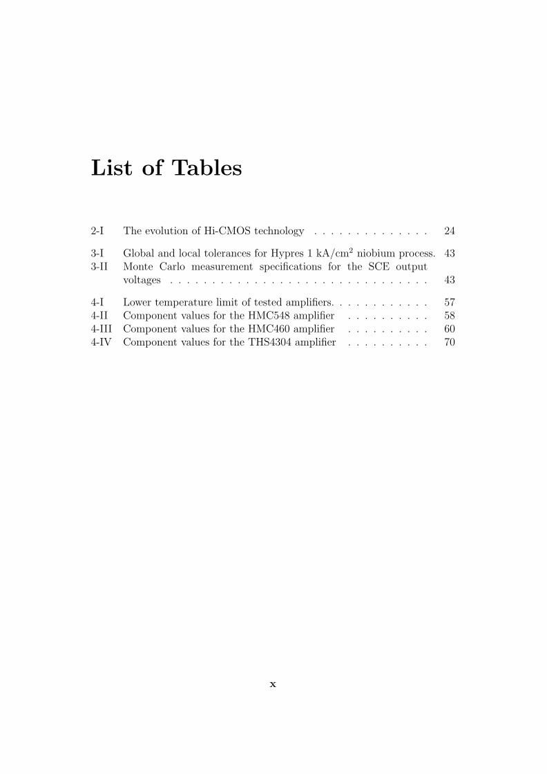
2-I The evolution of Hi-CMOS technology . . . . . . . . . . . . . . 24
3-I Global and local tolerances for Hypres 1 kA/cm2 niobium process. 433-II Monte Carlo measurement specifications for the SCE output
voltages . . . . . . . . . . . . . . . . . . . . . . . . . . . . . . . 43
4-I Lower temperature limit of tested amplifiers. . . . . . . . . . . . 574-II Component values for the HMC548 amplifier . . . . . . . . . . 584-III Component values for the HMC460 amplifier . . . . . . . . . . 604-IV Component values for the THS4304 amplifier . . . . . . . . . . 70
x
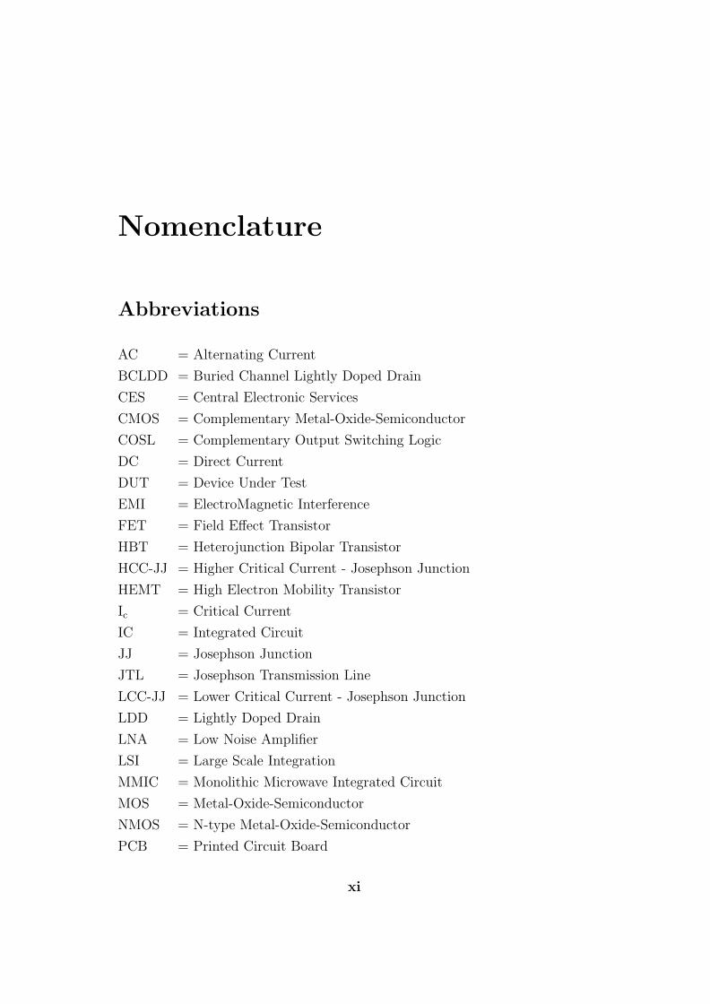
Nomenclature
Abbreviations
AC = Alternating Current
BCLDD = Buried Channel Lightly Doped Drain
CES = Central Electronic Services
CMOS = Complementary Metal-Oxide-Semiconductor
COSL = Complementary Output Switching Logic
DC = Direct Current
DUT = Device Under Test
EMI = ElectroMagnetic Interference
FET = Field Effect Transistor
HBT = Heterojunction Bipolar Transistor
HCC-JJ = Higher Critical Current - Josephson Junction
HEMT = High Electron Mobility Transistor
Ic = Critical Current
IC = Integrated Circuit
JJ = Josephson Junction
JTL = Josephson Transmission Line
LCC-JJ = Lower Critical Current - Josephson Junction
LDD = Lightly Doped Drain
LNA = Low Noise Amplifier
LSI = Large Scale Integration
MMIC = Monolithic Microwave Integrated Circuit
MOS = Metal-Oxide-Semiconductor
NMOS = N-type Metal-Oxide-Semiconductor
PCB = Printed Circuit Board
xi
NOMENCLATURE xii
p-HEMT = Pseudomorphic - High Electron Mobility Transistor
PMOS = P-type Metal-Oxide-Semiconductor
RF = Radio Frequency
RSFQ = Rapid Single Flux Quantum
SCE = SuperConductive Electronics
SFQ = Single Flux Quantum
SQUID = Superconducting Quantum Interference Device
SMA = Sub-Miniature version A
SMD = Surface Mount Device
SOIC = Small-Outline Integrated Circuit
SPICE = Simulation Program with Integrated Circuit Emphasis
Tc = Critical Temperature
Prefixes
p = pico = 10-12
n = nano = 10-9
µ = micro = 10-6
m = milli = 10-3
k = kilo = 103
M = mega = 106
G = giga = 109
Units
A = AmpereC = Degrees Celsius
eV = Electron-Volts (160.217 733 0·10-21 J)
Hz = Hertz
K = Kelvin
m = Meters
V = Volt
W = Watt
Ω = Ohm
Chapter 1
Introduction
1.1 Background
The field of applied superconductivity is young and exciting, with new
applications appearing regularly. Superconductivity is the phenomenon that
occurs in certain materials at extremely low temperatures. It is characterised
by exactly zero electrical resistance and the exclusion of the interior magnetic
field. At temperatures below the critical temperature (Tc), the resistance
disappears almost instantaneously. Each substance has its own critical
current ranging from 4.2 K (Mercury) up to 200 K (Sn6Ba4Ca2Cu10Oy) [4].
Superconducting electronics (SCE) outperform semiconductors in almost
every aspect, but require cryogenic cooling (which requires high vacuum
environments) and good magnetic shielding to operate.
Superconductors are used to build Josephson Junctions (JJ), the active device
in SCE [5]. It is a junction between two superconductors which is small
enough to allow only a slight overlap of the electron pair wave function of the
two superconductors. A non-stationary Josephson effect occurs if a constant
voltage U or a current larger than the so-called critical current (Ic) is applied
to the junction. The junction then acquires an active resistance. As noted by
[5] and explained further in section 2.1 on page 4 to be contrary to Ohm’s law,
I =U
R, (1.1)
1
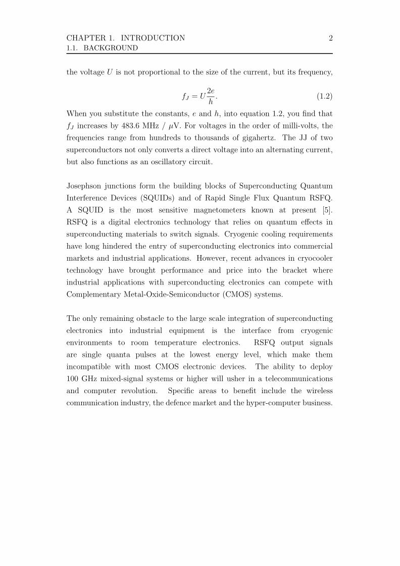
CHAPTER 1. INTRODUCTION 21.1. BACKGROUND
the voltage U is not proportional to the size of the current, but its frequency,
fJ = U2e
h. (1.2)
When you substitute the constants, e and h, into equation 1.2, you find that
fJ increases by 483.6 MHz / µV. For voltages in the order of milli-volts, the
frequencies range from hundreds to thousands of gigahertz. The JJ of two
superconductors not only converts a direct voltage into an alternating current,
but also functions as an oscillatory circuit.
Josephson junctions form the building blocks of Superconducting Quantum
Interference Devices (SQUIDs) and of Rapid Single Flux Quantum RSFQ.
A SQUID is the most sensitive magnetometers known at present [5].
RSFQ is a digital electronics technology that relies on quantum effects in
superconducting materials to switch signals. Cryogenic cooling requirements
have long hindered the entry of superconducting electronics into commercial
markets and industrial applications. However, recent advances in cryocooler
technology have brought performance and price into the bracket where
industrial applications with superconducting electronics can compete with
Complementary Metal-Oxide-Semiconductor (CMOS) systems.
The only remaining obstacle to the large scale integration of superconducting
electronics into industrial equipment is the interface from cryogenic
environments to room temperature electronics. RSFQ output signals
are single quanta pulses at the lowest energy level, which make them
incompatible with most CMOS electronic devices. The ability to deploy
100 GHz mixed-signal systems or higher will usher in a telecommunications
and computer revolution. Specific areas to benefit include the wireless
communication industry, the defence market and the hyper-computer business.
CHAPTER 1. INTRODUCTION 31.2. RESEARCH OBJECTIVES
1.2 Research Objectives
This thesis is aimed at testing commercially available CMOS amplifier
circuitry at 4 Kelvin, or -269 C. It would plot the S-parameters of different
amplifiers at 4 Kelvin. These parameters can then be used to design, verify
and construct interface electronics that can successfully operate at 4 K.
These electronics can form the basis of most SCE systems, as it would allow
out-of-lab usage of SCE systems in industrial environments.
1.3 Thesis Overview
Theoretical studies done showed that the problem can be solved in two parts.
First the RSFQ signal can be amplified with the use of superconducting
technology. Next the amplified signal can be further amplified with a CMOS
amplifier that operate at 4.2 K. The superconducting amplifier was designed
and will only be demonstrated with simulations and Monte Carlo analysis. A
prototype was not developed due to cost and time restrains.
The cryocooler was modified to accommodate RF input and output signals
through two SMA feed-through connectors. Various different commercially
available amplifier Integrated Circuits (IC’s) were tested inside the cryocooler.
The tests were performed with the DUT (device under test) at 4 K and
the cryo-cooler in full operation. The results were compared with the
room temperature equivalent results. Various different CMOS manufacturing
processes were tested and compared with each other. Pseudomorphic-High
Electron Mobility Transistors (p-HEMT) were also tested and compared.
Practical and simulation results are provided along with conclusions and
recommendations.
Chapter 2
Background and Specifications
Superconductive RSFQ electronics are capable of outperforming conventional
semiconductor electronics in terms of speed. Superconductive circuits are
always accommodated in a cooling system, therefore it is reasonable to cool
down the amplifier as well to cryogenic temperatures for the sake of noise
reduction and gain improvement. The interfacing of cryogenic electronics with
room temperature electronics is a challenging field for amplifier design.
2.1 Josephson Junctions
Josephson junctions are explained by [5]. Two superconductors are placed on
top of each other with a non-superconducting barrier placed between them. If
the barrier is sufficiently thin (a few nano meters) electrons can pass from one
superconductor to the other, although a non-conducting layer exist between
the two layers. That is thanks to the quantum mechanical tunneling effect.
The wave function, describing the probability of finding an electron, leaks out
from the metallic region. If a second metal is brought into this zone, a current
can flow across this sandwich structure.
Due to the tunneling electrons, the two superconductors are coupled to each
other and a weak supercurrent (Josephson current) can flow across the barrier.
A superconductor can carry only a limited constant electric current called
the critical current (Ic). Divided by the contact area, we have the critical
current density Jc. When an applied current exceeds the Jc of the Josephson
4
CHAPTER 2. BACKGROUND AND SPECIFICATIONS 52.2. SQUID DEVICES
Junction, it returns to its resistive state.
If a direct voltage U is applied to the sandwich, the gauge-invariant phase
difference increases as a function of time. That gives a high-frequency
alternating current, the frequency of which is given by,
fJ = U2e
h. (2.1)
Fundamental constants h and e allows us to define the ratio of the junction
frequency (fJ) and the applied voltage as 483.6 MHZ / µV.
2.2 SQUID Devices
For SQUID operation, two phenomena are of importance. These are
the stationary Josephson effect and the conservation and quantisation
of a magnetic flux in a superconducting ring. A SQUID consist of a
superconducting ring with one (RF-SQUID) or two (DC-SQUID) Josephson
Junctions in parallel.
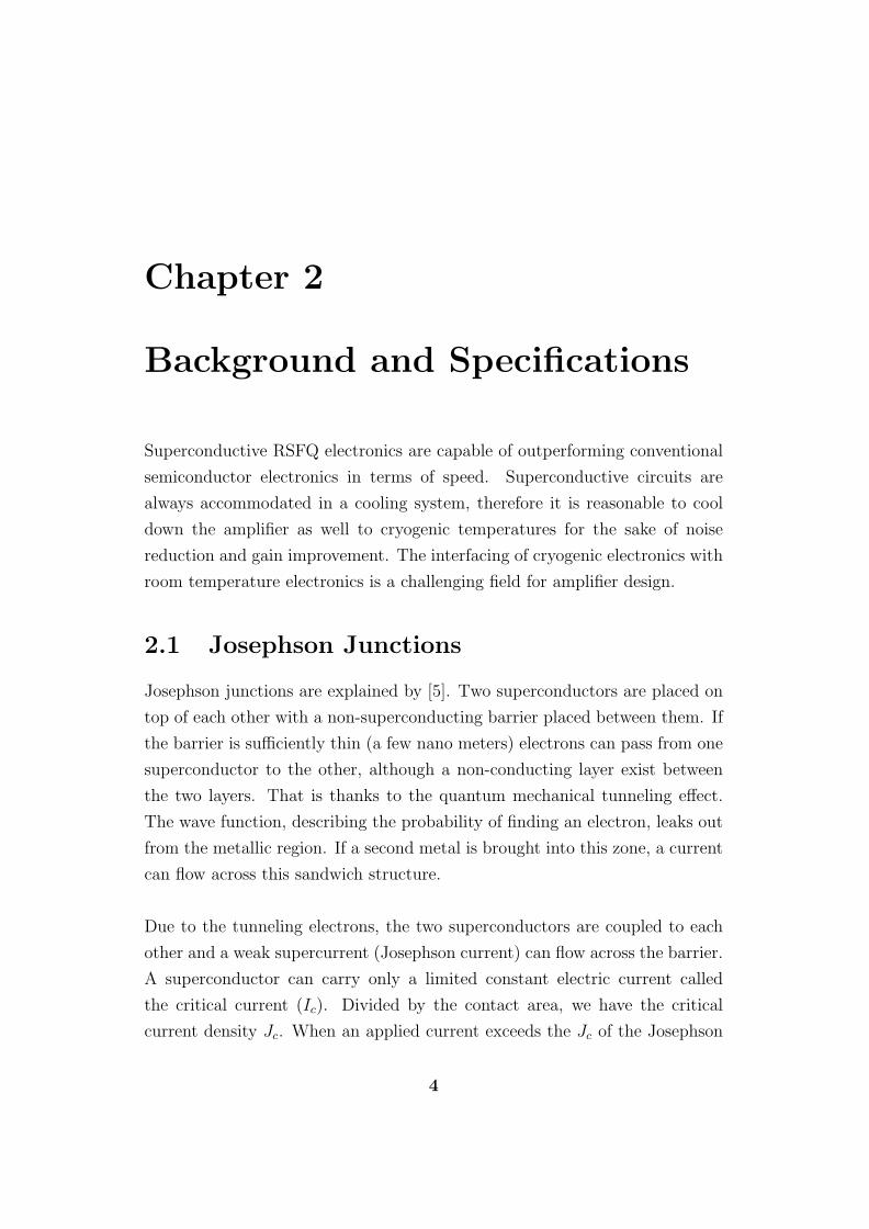
Figure 2.1 shows the circuit layout of a DC-SQUID. The ring is located in a
magnetic field oriented perpendicular to the area of the ring. A bias current
(I) flows along the ring. By measuring the voltage drop across the Josephson
junction, we can determine the maximum current that can be carried by the
ring. This maximum current oscillates as a function of the applied magnetic
field or the flux through the ring [5]. An outlet and inlet provides access to
the SQUID for current biasing. A DC-SQUID is much more sensitive and
stable than a RF-SQUID.
CHAPTER 2. BACKGROUND AND SPECIFICATIONS 62.3. RSFQ SIGNALS
JJ1 JJ2
Biascurrent
V
Figure 2.1: Circuit layout of a DC-SQUID.
2.3 RSFQ Signals
As mentioned in Chapter 1, SCE technology holds great potential for the
future. RSFQ is a digital electronics technology that relies on quantum effects
in superconducting materials to switch signals. A slightly overcritical current
is applied to an over damped junction. The Josephson alternating currents
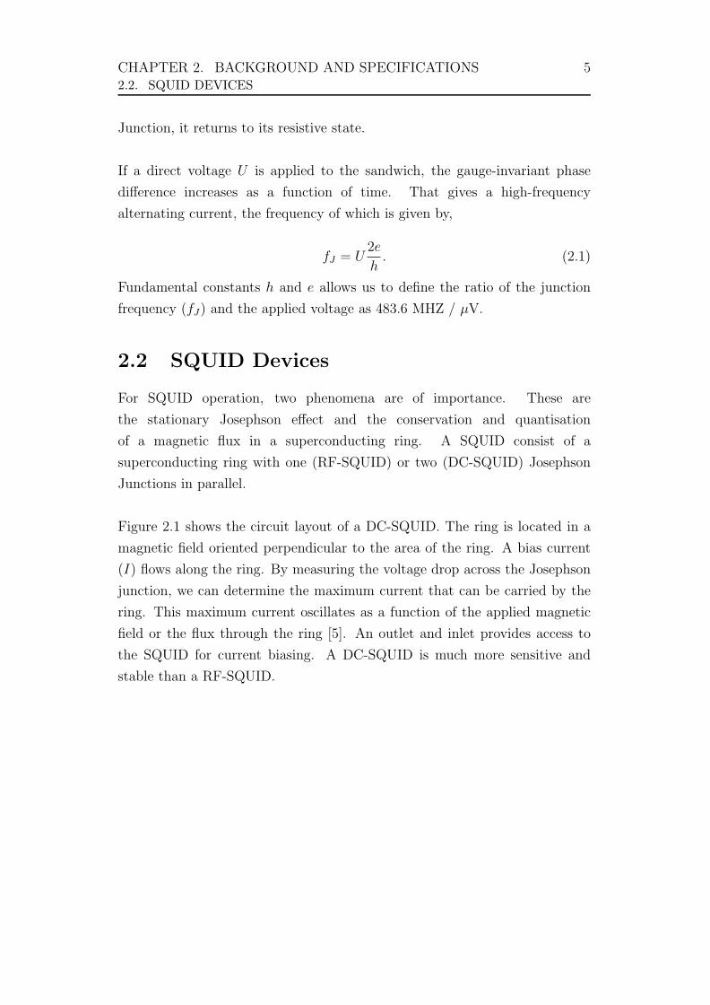
flow across the junction in the form of a short pulse (SFQ pulse). According
to [5] the width of the pulse is φ0/IcR. In their example IcR = 1 mV. That gave
a pulse width of about 2 ps. During a pulse, the phase difference γ changes
by 2φ. According to the second Josephson equation,
γ = (2π
φ0
)U, (2.2)
this phase leads to a voltage pulse. The area under the pulse, integrated over
time, amounts to φ0 ≈ 2.07 mV.ps. Figure 2.2 shows an amplitude against
time graph of a single SFQ pulse.
CHAPTER 2. BACKGROUND AND SPECIFICATIONS 72.3. RSFQ SIGNALS
10 20 30 40 500-0.2
0.0
0.2
0.4
0.6
0.8
Time [ps]
Am
plitu
de [m
V]
Figure 2.2: Amplitude against time graph of a single SFQ pulse
RSFQ is different from traditional CMOS transistors in the following ways [5]:
• It is based on superconductors, so a cryogenic environment is required.
• Instead of voltage levels, digital signals are represented in picosecond
duration pulses. The system is synchronised with a pre-determined clock
frequency. If a pulse arrives within a cycle given by the clock, then this
corresponds to a 1. If no pulse arrives, this corresponds to a 0.
• The quantum pulses are switched by Josephson junctions.
• Signals cannot be split into multiple outputs without active circuit
elements.
RSFQ relies on another intrinsic property of superconductors (apart from the
loss of resistance below a critical temperature Tc). Within a closed section of
superconducting material any magnetic flux present can exist only in discrete
amounts that are multiples of the magnetic flux quantum
CHAPTER 2. BACKGROUND AND SPECIFICATIONS 82.4. LOW TEMPERATURE MEASUREMENTS
Φ0 = h/2e ≈ 2.07× 10⁻¹⁵Wb, (2.3)
where h is Planck’s constant and e is the electron charge [6].
The RSFQ signal was simulated in WRSpice by [7] with a DC-to-RSFQ
converter. The RSFQ pulse generator feeds SFQ pulses of a short rise time
(tr = tf ≈ 10 ps) and a small voltage amplitude of about 400 µV. The SFQ
pulses form a bit pattern with different bit lengths and a clock frequency,
fclock = 100 MHz.
2.4 Low Temperature Measurements
Operating conditions for RSFQ and Complementary Output Switching Logic
(COSL) families are usually inside vacuumed cryocoolers or liquid helium
cryostats at cryogenic temperatures. Niobium based RSFQ electronics operate
at 4.2 K or below.
Performing measurements at cryogenic temperatures is a very challenging
task. Measurements can be done with the use of a cryo dipstick, a temperature
measurement control unit, a bottle of liquid helium and various instruments
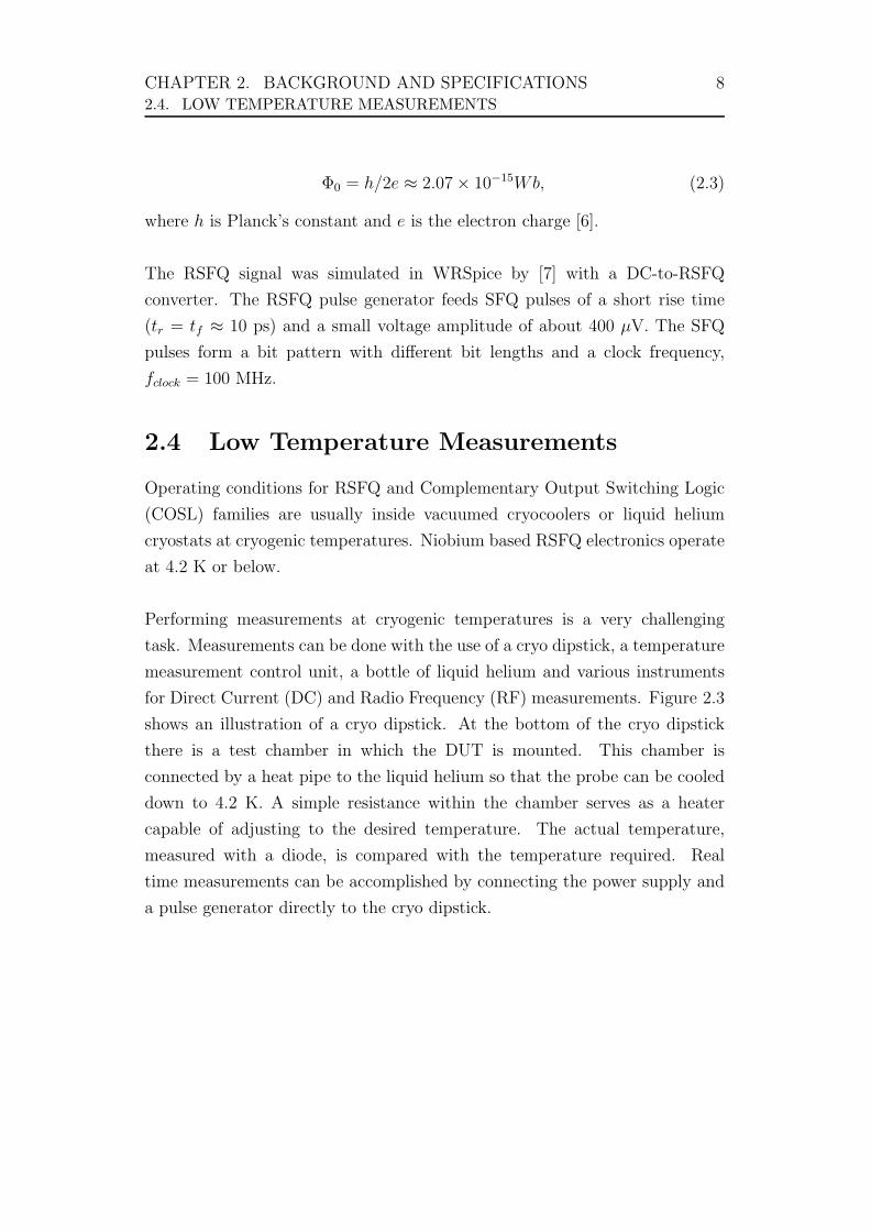
for Direct Current (DC) and Radio Frequency (RF) measurements. Figure 2.3
shows an illustration of a cryo dipstick. At the bottom of the cryo dipstick
there is a test chamber in which the DUT is mounted. This chamber is
connected by a heat pipe to the liquid helium so that the probe can be cooled
down to 4.2 K. A simple resistance within the chamber serves as a heater
capable of adjusting to the desired temperature. The actual temperature,
measured with a diode, is compared with the temperature required. Real
time measurements can be accomplished by connecting the power supply and
a pulse generator directly to the cryo dipstick.
CHAPTER 2. BACKGROUND AND SPECIFICATIONS 92.5. CRYOREFRIGERATOR
Liquid Helium
Dipstick
DUT
Vacuum
Figure 2.3: Illustration of a Cryo Dipstick.
2.5 Cryorefrigerator
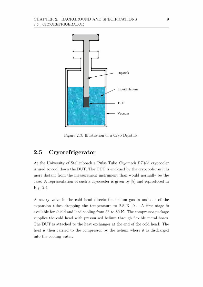
At the University of Stellenbosch a Pulse Tube Cryomech PT405 cryocooler
is used to cool down the DUT. The DUT is enclosed by the cryocooler so it is
more distant from the measurement instrument than would normally be the
case. A representation of such a cryocooler is given by [8] and reproduced in
Fig. 2.4.
A rotary valve in the cold head directs the helium gas in and out of the
expansion tubes dropping the temperature to 2.8 K [9]. A first stage is
available for shield and lead cooling from 35 to 80 K. The compressor package
supplies the cold head with pressurised helium through flexible metal hoses.
The DUT is attached to the heat exchanger at the end of the cold head. The
heat is then carried to the compressor by the helium where it is discharged
into the cooling water.
CHAPTER 2. BACKGROUND AND SPECIFICATIONS 102.5. CRYOREFRIGERATOR
Compressor4 K
Cold Finger
2nd Stage
1st Stageat 60 K
Figure 2.4: Representation of the Cryomech PT405 cryocooler
The two-stage cryocooler delivers 25 W of cooling power at 65 K and 0.5 W
at 4.2 K. Heat sources include electric power dissipation, thermal radiation
losses, poorly vacuumed space and heat transferring cables. Multiple thermal
shields and a good vacuum (10−5 bar), is necessary for reduced heating, but
the heat flow through cabling from the outside of the cryocooler still conducts
heat into the system. The correct cables should be selected that are sufficient
for RF signals and will not conduct too much heat into the system.
The semiconductor electronic devices were tested in the 2nd stage of the
cryocooler on the cold finger to get it as close as possible to the actual SCE.
The design also needs to be compact in order to fit into the confined space
of the 2nd stage. When the amplifier is implemented inside the 2nd stage, the
semiconductor electronics is also cooled down to 4 K and the thermal noise on
the SCE circuits is significantly less. A theorem by Nyquist [10] states that
the mean-square noise voltage appearing across the terminals of a resistor of
CHAPTER 2. BACKGROUND AND SPECIFICATIONS 112.6. SUZUKI STACK AMPLIFIER
R Ω at temperature T Kelvin in a frequency band B hertz is giving by
V 2rms = 4kTRBV 2, (2.4)
where k = Boltzmann’s constant, relating temperature to energy. Thus, when
temperature is reduced, the noise is also reduced thereby creating a more
sensitive measurement system.
Measurement accuracy is deteriorated by cable losses and ElectroMagnetic
Interference (EMI). EMI could occur due to poor cable shielding [11].
Another aspect is calibration, which is made at room temperature. Cooling
down the DUT will change the characteristic of the measurement system.
Consequently, appropriate cables must be chosen which have electrical
properties independent of temperature. If this is the case, the performed
calibration is also valid for measurements at cryogenic temperatures. Care
has to be taken that the heat conducted into the cryocooler by the cables
does not exceed the heat removal capacity.
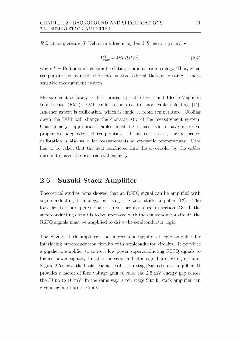
2.6 Suzuki Stack Amplifier
Theoretical studies done showed that an RSFQ signal can be amplified with
superconducting technology by using a Suzuki stack amplifier [12]. The
logic levels of a superconductor circuit are explained in section 2.3. If the
superconducting circuit is to be interfaced with the semiconductor circuit, the
RSFQ signals must be amplified to drive the semiconductor logic.
The Suzuki stack amplifier is a superconducting digital logic amplifier for
interfacing superconductor circuits with semiconductor circuits. It provides
a gigahertz amplifier to convert low power superconducting RSFQ signals to
higher power signals, suitable for semiconductor signal processing circuits.
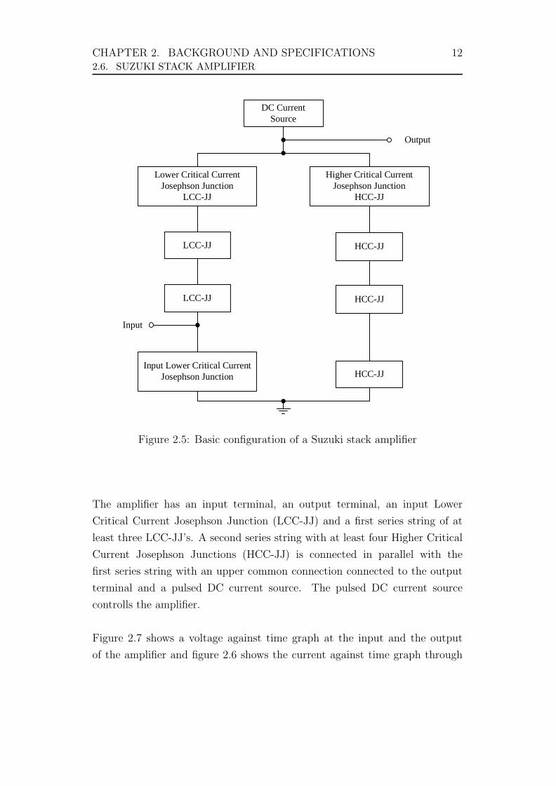
Figure 2.5 shows the basic schematic of a four stage Suzuki stack amplifier. It
provides a factor of four voltage gain to raise the 2.5 mV energy gap across
the JJ up to 10 mV. In the same way, a ten stage Suzuki stack amplifier can
give a signal of up to 25 mV.
CHAPTER 2. BACKGROUND AND SPECIFICATIONS 122.6. SUZUKI STACK AMPLIFIER
DC CurrentSource
Lower Critical CurrentJosephson Junction
LCC-JJ
Higher Critical CurrentJosephson Junction
HCC-JJ
LCC-JJ
LCC-JJ
Input Lower Critical CurrentJosephson Junction
HCC-JJ
HCC-JJ
HCC-JJ
Input
Output
Figure 2.5: Basic configuration of a Suzuki stack amplifier
The amplifier has an input terminal, an output terminal, an input Lower
Critical Current Josephson Junction (LCC-JJ) and a first series string of at
least three LCC-JJ’s. A second series string with at least four Higher Critical
Current Josephson Junctions (HCC-JJ) is connected in parallel with the
first series string with an upper common connection connected to the output
terminal and a pulsed DC current source. The pulsed DC current source
controlls the amplifier.
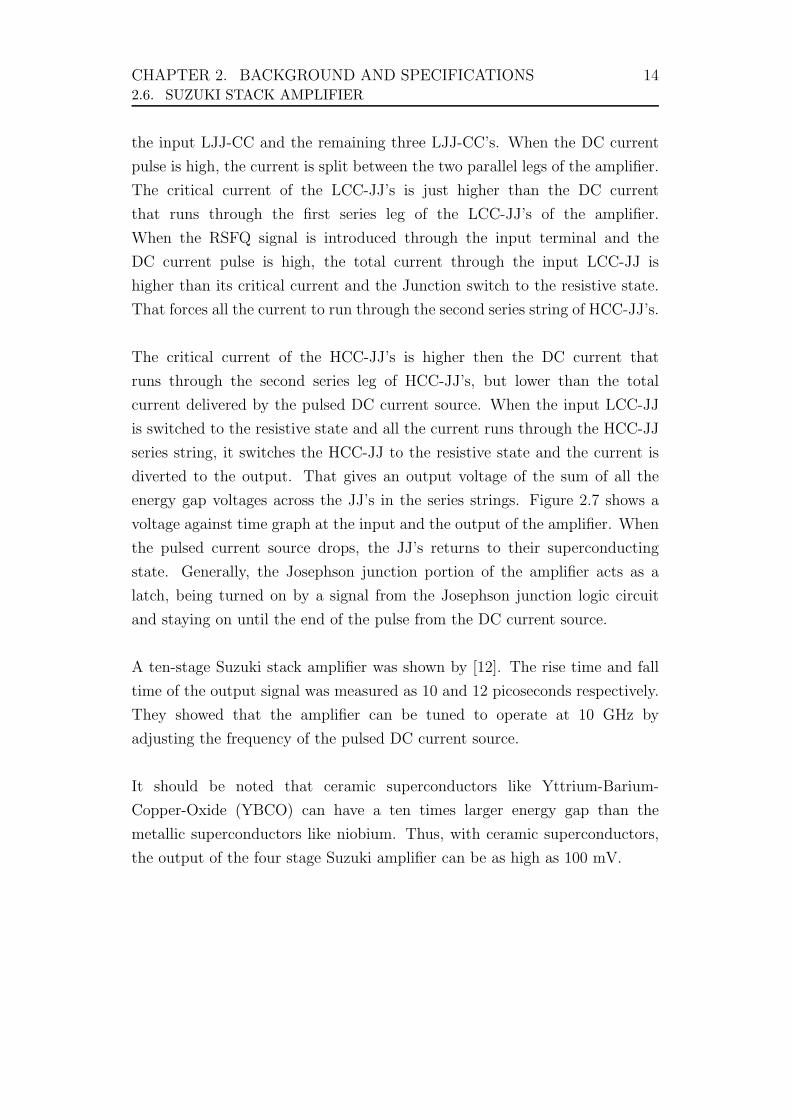
Figure 2.7 shows a voltage against time graph at the input and the output
of the amplifier and figure 2.6 shows the current against time graph through
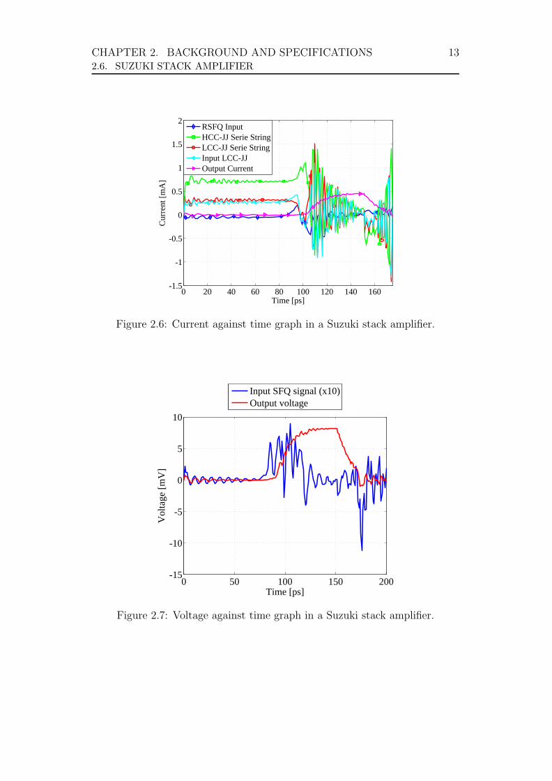
CHAPTER 2. BACKGROUND AND SPECIFICATIONS 132.6. SUZUKI STACK AMPLIFIER
0 20 40 60 80 100 120 140 160-1.5
-1
-0.5
0
0.5
1
1.5
2
Time [ps]
Cur
rent
[mA
]
RSFQ InputHCC-JJ Serie StringLCC-JJ Serie StringInput LCC-JJOutput Current
Figure 2.6: Current against time graph in a Suzuki stack amplifier.
0 50 100 150 200-15
-10
-5
0
5
10
Time [ps]
Vol
tage
[mV
]
Input SFQ signal (x10)Output voltage
Figure 2.7: Voltage against time graph in a Suzuki stack amplifier.
CHAPTER 2. BACKGROUND AND SPECIFICATIONS 142.6. SUZUKI STACK AMPLIFIER
the input LJJ-CC and the remaining three LJJ-CC’s. When the DC current
pulse is high, the current is split between the two parallel legs of the amplifier.
The critical current of the LCC-JJ’s is just higher than the DC current
that runs through the first series leg of the LCC-JJ’s of the amplifier.
When the RSFQ signal is introduced through the input terminal and the
DC current pulse is high, the total current through the input LCC-JJ is
higher than its critical current and the Junction switch to the resistive state.
That forces all the current to run through the second series string of HCC-JJ’s.
The critical current of the HCC-JJ’s is higher then the DC current that
runs through the second series leg of HCC-JJ’s, but lower than the total
current delivered by the pulsed DC current source. When the input LCC-JJ
is switched to the resistive state and all the current runs through the HCC-JJ
series string, it switches the HCC-JJ to the resistive state and the current is
diverted to the output. That gives an output voltage of the sum of all the
energy gap voltages across the JJ’s in the series strings. Figure 2.7 shows a
voltage against time graph at the input and the output of the amplifier. When
the pulsed current source drops, the JJ’s returns to their superconducting
state. Generally, the Josephson junction portion of the amplifier acts as a
latch, being turned on by a signal from the Josephson junction logic circuit
and staying on until the end of the pulse from the DC current source.
A ten-stage Suzuki stack amplifier was shown by [12]. The rise time and fall
time of the output signal was measured as 10 and 12 picoseconds respectively.
They showed that the amplifier can be tuned to operate at 10 GHz by
adjusting the frequency of the pulsed DC current source.
It should be noted that ceramic superconductors like Yttrium-Barium-
Copper-Oxide (YBCO) can have a ten times larger energy gap than the
metallic superconductors like niobium. Thus, with ceramic superconductors,
the output of the four stage Suzuki amplifier can be as high as 100 mV.
CHAPTER 2. BACKGROUND AND SPECIFICATIONS 152.7. DC SQUID AMPLIFIER
2.7 DC SQUID Amplifier
A DC SQUID is the most sensitive detector of magnetic flux available [13].
Any physical quantity that can be converted to magnetic flux, e.g., current
or magnetic field, can be measured using a SQUID. Although DC SQUID’s
are inherently capable of amplifying signals at frequencies from DC to a few
GHz, [13] showed that the coupling techniques necessary to match the SQUID
output signal to room temperature electronics severely limit the usable
bandwidth. A transformer or resonant circuit, with Alternating Current
(AC) flux modulation and lock-in detection, is usually used to step up the
SQUID voltage to the required level. This technique generally limits the
bandwidth to tens of kHz, and requires complex room temperature electronics.
Two-stage SQUID amplifiers in which a second SQUID is used to amplify the
output of the first have been reported [14]. The gain of the second SQUID
is sufficient to make the amplified noise of the first SQUID larger than the
intrinsic noise of the second SQUID. A matching transformer is still required
at the output of the second SQUID stage to achieve a better low-temperature
gain.
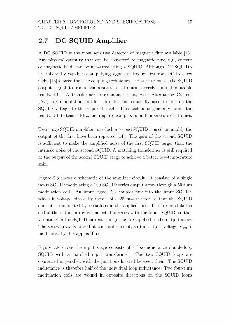
Figure 2.8 shows a schematic of the amplifier circuit. It consists of a single
input SQUID modulating a 100-SQUID series output array through a 50-turn
modulation coil. An input signal Isig couples flux into the input SQUID,
which is voltage biased by means of a 25 mΩ resistor so that the SQUID
current is modulated by variations in the applied flux. The flux modulation
coil of the output array is connected in series with the input SQUID, so that
variations in the SQUID current change the flux applied to the output array.
The series array is biased at constant current, so the output voltage Vout is
modulated by this applied flux.
Figure 2.8 shows the input stage consists of a low-inductance double-loop
SQUID with a matched input transformer. The two SQUID loops are
connected in parallel, with the junctions located between them. The SQUID
inductance is therefore half of the individual loop inductance. Two four-turn
modulation coils are wound in opposite directions on the SQUID loops
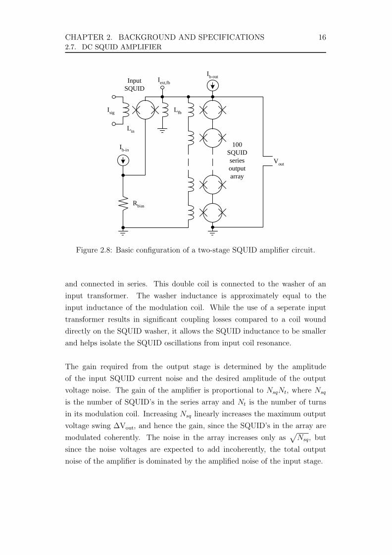
CHAPTER 2. BACKGROUND AND SPECIFICATIONS 162.7. DC SQUID AMPLIFIER
InputSQUID
Isig
100SQUIDseriesoutputarray
Vout
Rbias
Lin
Ib-in
Iext,fb
Lfb
Ib-out
Figure 2.8: Basic configuration of a two-stage SQUID amplifier circuit.
and connected in series. This double coil is connected to the washer of an
input transformer. The washer inductance is approximately equal to the
input inductance of the modulation coil. While the use of a seperate input
transformer results in significant coupling losses compared to a coil wound
directly on the SQUID washer, it allows the SQUID inductance to be smaller
and helps isolate the SQUID oscillations from input coil resonance.
The gain required from the output stage is determined by the amplitude
of the input SQUID current noise and the desired amplitude of the output
voltage noise. The gain of the amplifier is proportional to NsqNt, where Nsq
is the number of SQUID’s in the series array and Nt is the number of turns
in its modulation coil. Increasing Nsq linearly increases the maximum output
voltage swing ∆Vout, and hence the gain, since the SQUID’s in the array are
modulated coherently. The noise in the array increases only as√
Nsq, but
since the noise voltages are expected to add incoherently, the total output
noise of the amplifier is dominated by the amplified noise of the input stage.
CHAPTER 2. BACKGROUND AND SPECIFICATIONS 172.8. CMOS AMPLIFIERS
Nsq and Nt may be chosen to maximise the bandwidth and the dynamic range.
The bandwidth of the two-stage amplifier is determined by the lowest cut-off
frequency in the system,
fc = Rdyn/2ΠLin, (2.5)
where Rdyn is the dynamic resistance of the input SQUID and Lin is the
input inductance of the output array modulation coil. This input inductance
is proportional to Nt2NsqLsq, where Lsq is the inductance of a single SQUID
in the output array. Since Lin increases more rapidly with Nt than with
Nsq, it is best to achieve the required gain by increasing Nsq rather than Nt.
Increasing Nsq maximises the dynamic range since ∆Vout increases.
A 100-SQUID series array with an input transformer with 36 primary turns
was shown by [15] to have a bandwidth of at least 175 MHz when operated
alone.
2.8 CMOS Amplifiers
A CMOS amplifier is needed that can operate at 4.2 K. Several advantages are
shown by [1] in CMOS devices operating at low temperatures. First the carrier
mobility is increased due to decreased lattice scattering at low temperatures,
resulting in the enhancement of device current and switching speed. The
junction capacitances are also reduced at low temperatures due to carrier
freeze-out. For the same reason, leakage currents decrease exponentially with
decreasing temperature. This results in the reduced sub-threshold coefficient
α and an increase in the threshold voltage, which suggests a very small
voltage operation is feasible with careful adjustment of threshold voltages.
The threshold voltage variation is symmetrical, and consequently CMOS logic
has a very wide temperature range of operation. This suggests that CMOS
circuits for low-temperature operation can be adjusted and matched at room
temperature.
CHAPTER 2. BACKGROUND AND SPECIFICATIONS 182.8. CMOS AMPLIFIERS
Field effect mobility was measured by [1] from transconductance at low
drain voltages. In the long-channel case, the increase was about a factor
of six larger for liquid nitrogen temperatures (77 K) compared to room
temperature measurements, while a factor of eight was observed at liquid
helium temperatures (4.2 K). However, for the short-channel case, the
mobility increase appears to be smaller than in the long-channel case.
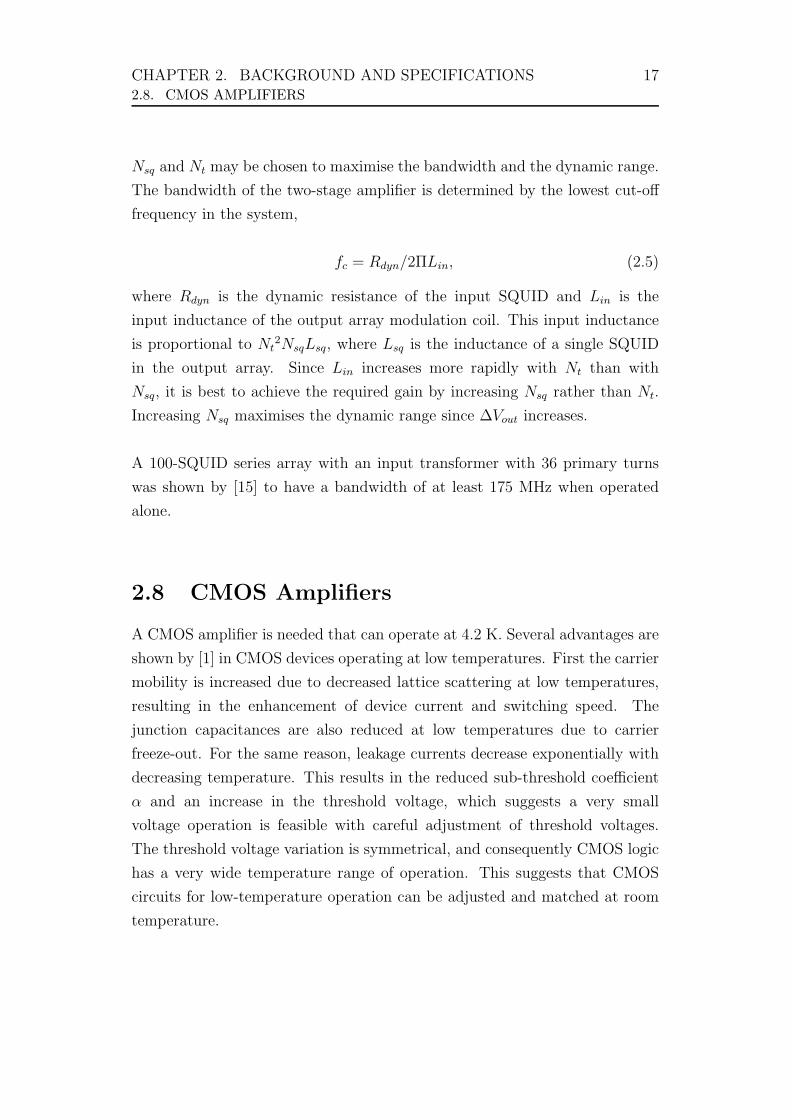
Figure 2.9 shows the subthreshold current characteristics of the Metal Oxide
Semiconductor (MOS) transistor pair tested by [1]. The current-voltages
characteristics showed that a lowering in the temperature meant the channel
conductance of both transistors would increase very symmetrically. This
means that the proper design ratio can be maintained even at cryogenic
temperatures. It can be seen from a practical viewpoint that with cooling
down, there is a great beneficial effect on the transconductance (gm) increase.
Liquid Helium
Dipstick
DUT
Vacuum
77 K
Figure 2.9: Subthreshold current characteristics as cited in [1].
CHAPTER 2. BACKGROUND AND SPECIFICATIONS 192.8. CMOS AMPLIFIERS
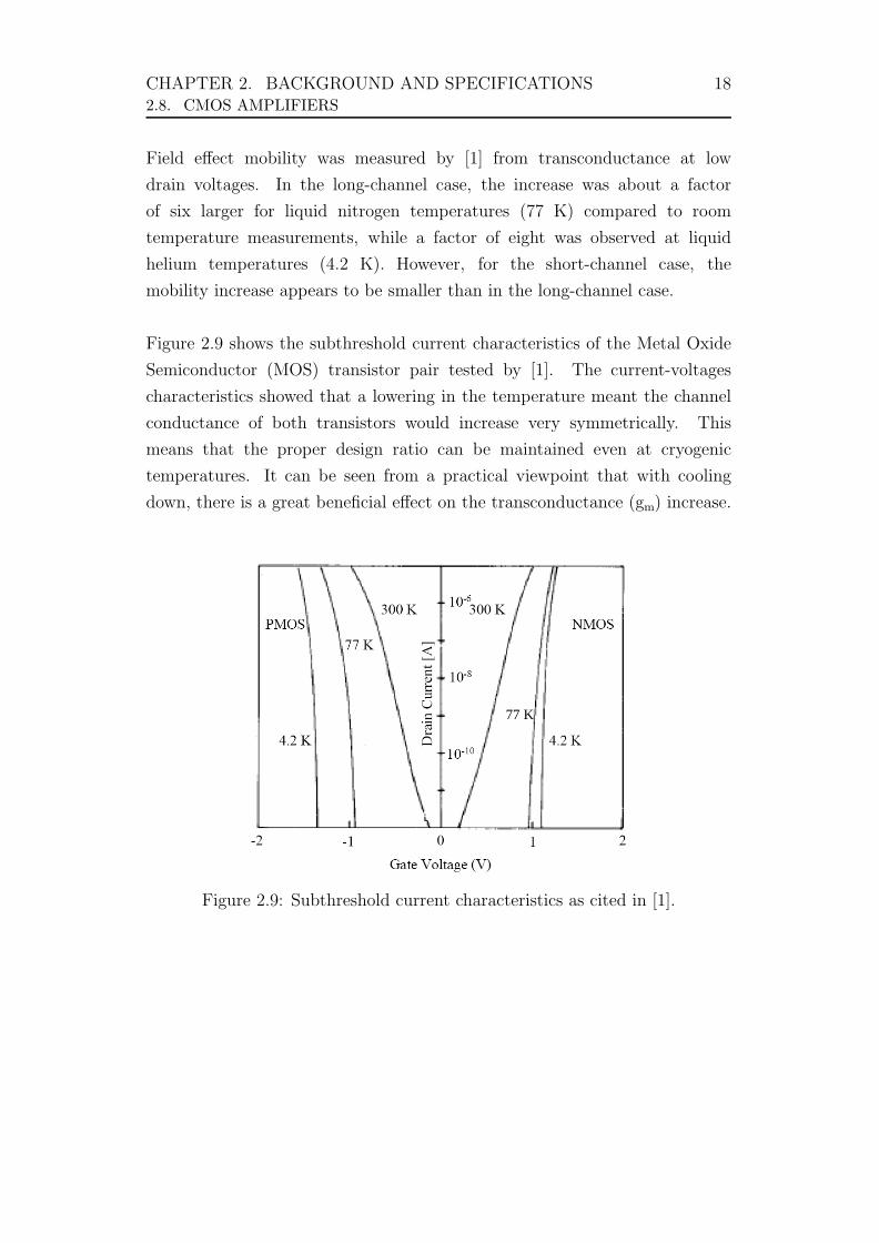
Figure 2.10 shows the cross section of a CMOS transistor. Variations in sheet
resistances was tested by [1].
Al Poly-Si
n-Well P-Well
n-sub
PSGP+ n+ n+SiO2P+
Figure 2.10: Cross section of a CMOS transistor pair as cited in [1].
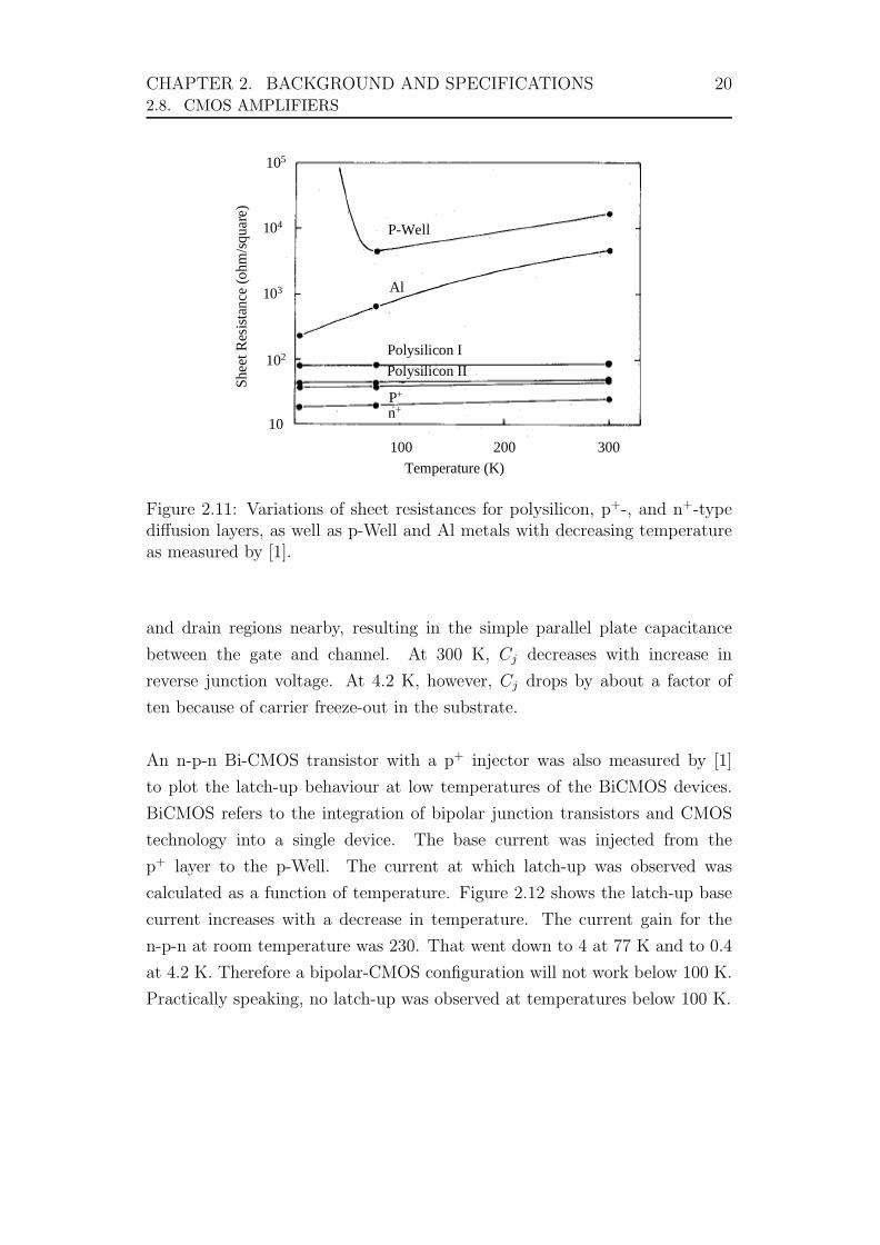
Figure 2.11 shows the variations of the sheet resistances for polysilicon, p+-
and n+-type diffusion layers as well as p-Well and Aluminium (Al) metals
with decreasing temperature. In low impurity concentration situations, such
as p-Well, the resistivity decreases due to an increase of mobility down to 77
K. However, carrier freeze-out causes a steep increase in p-Well resistivity at
4.2 K. The p-Well resistance increases above 1010 ohm/square. at 4.2 K. [1]
Other resistance drop with decreasing temperature down to 4.2 K. In
particular, Aluminium metal resistance drops drastically because of reduced
lattice vibrations. This gives a great advantage to reducing noise caused by
CMOS switching and power supply line resistance.
The gate capacitance (CG) and junction capacitance (Cj) was measured by
[2]. They found that the capacitance decreases with decrease in temperature
in the depletion region (VG < 0 V), while there is almost no temperature
dependence in the inversion region (VG > 0 V). The reduction of CG in the
depletion region is due to the carrier freeze-out effect, which means that
all extra electrons and holes are captured by their dopant atoms. In the
inverse region the extra electrons are provided from the heavily doped source
CHAPTER 2. BACKGROUND AND SPECIFICATIONS 202.8. CMOS AMPLIFIERS
104
105
103
102
10100 200 300
P-Well
Al
Polysilicon IPolysilicon II
P+
n+
Temperature (K)
Shee
t Res
istan
ce (o
hm/sq
uare
)
Figure 2.11: Variations of sheet resistances for polysilicon, p+-, and n+-typediffusion layers, as well as p-Well and Al metals with decreasing temperatureas measured by [1].
and drain regions nearby, resulting in the simple parallel plate capacitance
between the gate and channel. At 300 K, Cj decreases with increase in
reverse junction voltage. At 4.2 K, however, Cj drops by about a factor of
ten because of carrier freeze-out in the substrate.
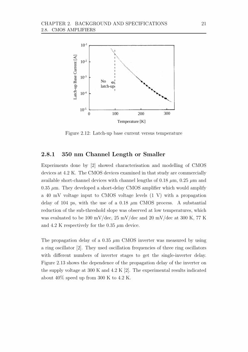
An n-p-n Bi-CMOS transistor with a p+ injector was also measured by [1]
to plot the latch-up behaviour at low temperatures of the BiCMOS devices.
BiCMOS refers to the integration of bipolar junction transistors and CMOS
technology into a single device. The base current was injected from the
p+ layer to the p-Well. The current at which latch-up was observed was
calculated as a function of temperature. Figure 2.12 shows the latch-up base
current increases with a decrease in temperature. The current gain for the
n-p-n at room temperature was 230. That went down to 4 at 77 K and to 0.4
at 4.2 K. Therefore a bipolar-CMOS configuration will not work below 100 K.
Practically speaking, no latch-up was observed at temperatures below 100 K.
CHAPTER 2. BACKGROUND AND SPECIFICATIONS 212.8. CMOS AMPLIFIERS
Nolatch-up
Temperature [K]
Latc
h-up
Bas
e C
urre
nt [A
]
0 100 200 30010-5
10-4
10-3
10-2
10-1
Figure 2.12: Latch-up base current versus temperature
2.8.1 350 nm Channel Length or Smaller
Experiments done by [2] showed characterisation and modelling of CMOS
devices at 4.2 K. The CMOS devices examined in that study are commercially
available short-channel devices with channel lengths of 0.18 µm, 0.25 µm and
0.35 µm. They developed a short-delay CMOS amplifier which would amplify
a 40 mV voltage input to CMOS voltage levels (1 V) with a propagation
delay of 104 ps, with the use of a 0.18 µm CMOS process. A substantial
reduction of the sub-threshold slope was observed at low temperatures, which
was evaluated to be 100 mV/dec, 25 mV/dec and 20 mV/dec at 300 K, 77 K
and 4.2 K respectively for the 0.35 µm device.
The propagation delay of a 0.35 µm CMOS inverter was measured by using
a ring oscillator [2]. They used oscillation frequencies of three ring oscillators
with different numbers of inverter stages to get the single-inverter delay.
Figure 2.13 shows the dependence of the propagation delay of the inverter on
the supply voltage at 300 K and 4.2 K [2]. The experimental results indicated
about 40% speed up from 300 K to 4.2 K.
CHAPTER 2. BACKGROUND AND SPECIFICATIONS 222.8. CMOS AMPLIFIERS
0
20
40
60
80
100
2.5 3 3.5 4 4.5
300 K
4 K
VDD [V]
Prop
agat
ion
dela
y [p
s]
Figure 2.13: Dependence of the propagation delay of a CMOS inverterfabricated by a 0.35 µm CMOS process on the supply voltage at 300 K and4 K [2].
Based on these results, they estimated the power dissipation of the CMOS
transistor at 4.2 K. The power consumption of the CMOS circuit was
calculated with,
P = CLV 2DDf, (2.6)
where CL is the total load capacitance, f is the clock frequency and VDD is
the positive supply voltage. From figure 2.13, one can calculate a maximum
improvement. When VDD is reduced with 20 % (from 3.5 V to 2.8 V), the
propagation delay increases with /mbox30 %. Thus the clock frequency
also increases with 30 %. CL is composed of CG, Cj and the wiring
capacitance. Because the wiring capacitance and Cj are reduced substantially
at low temperature, they measured a 50% reduction of CL at cryogenic
temperatures. Putting all the values into eq 2.6, shows that a 60% reduction
in the power consumption is expected at 4.2 K.
CHAPTER 2. BACKGROUND AND SPECIFICATIONS 232.8. CMOS AMPLIFIERS
2.8.2 Hi-CMOS Technology
Further experiments were done by [1]. The paper reports on low-power
consumption high-speed operation of bulk CMOS devices at 77 K and 4.2 K.
The samples were fabricated using the Hi-CMOS II process which has been
applied to several practical large scale integration (LSI) circuits.
The n-channel MOS transistor is formed in a p-Well and the source-drain
diffusion layers are made through arsenic and phosphorus double implants.
P-channel devices are formed in an n-Well and the source drain diffusion layers
are made by boron implantation. Both of these transistors have n+ -doped
polysilicon gates with a gate length of 2 µm. The gate oxide thickness is 35 nm.
The substrate is 10 Ω.cm n-type. Throughout their experiments, surface ohmic
contacts were used both in the p-Well and n-Well to stabilise the potential.
The chips were diced and mounted on dual in-line ceramic packages with no
package seals. Measurements of electrical characteristics were made using
samples immersed directly into liquid nitrogen (77 K) or liquid helium (4.2 K).
They found that with cooling down of the Hi-CMOS II circuit, the power
dissipation decreased by up to 20%, while the propagation delay decreased by
up to 40%. The propagation delay indicates a useful improvement between
77 K and 4.2 K, while MOS characteristics do not change appreciably.
Hi-CMOS III technology is explained by [16]. It is the 2/3 scaling of Hi-CMOS
II with constant voltage, Lightly Doped Drain (LDD) N-type Metal Oxide
Semiconductor (NMOS) and newly developed Buried Channel Lightly Doped
Drain (BCLDD) P-type Metal Oxide Semiconductor (PMOS), with polycite
gate area adopted to reduce short channel effects and delays in interconnection
lines. Post-contact doping was also adopted to allow the overlap of contact
holes and diffusion edges and to reduce contact resistance.
Hi-CMOS III main features are summarised in Table 2-I and compared with
Hi-CMOS I and Hi-CMOS II.
CHAPTER 2. BACKGROUND AND SPECIFICATIONS 242.8. CMOS AMPLIFIERS
Table 2-I: The evolution of Hi-CMOS technology
Hi-CMOS I Hi-CMOS II Hi-CMOS III
Supply Voltage [V] 5 5 5
Gate length [µm] 3.0 2.0 1.2
NMOS structure Phos. Dif. Graded Drain LDD
PMOS structure Boron Dif. Boron Dif BCLDD
Gate oxide thickness [nm] 50 35 25
Field oxide thickness [nm] 650 650 650
Junction depth N-layer [µm] 0.50 0.35 0.25
Junction depth P-layer [µm] 0.50 0.40 0.40
Gate (width/space) [µm] 3.0/3.0 2.0/2.0 1.2/1.4
Al (width/space) [µm] 3.0/4.0 3.0/2.0 1.3/1.6
Contact hole [µm] 3.5 2.0 1.2
Saturation current NMOS [A/m] 107 164 255
Saturation current PMOS [A/m] 49 72 118
NMOS BVds [V] 10.5 9 9.5
2.8.3 p-HEMT
In general, to allow conduction, semiconductors need to be doped with
impurities to generate mobile electrons in the layer. This causes electrons
to slow down because they end up colliding with the impurities which were
used to generate them in the first place. HEMT (High Electron Mobility
Transistor), however, is a smart device to resolve this seemingly inherent
unsolved contradiction.
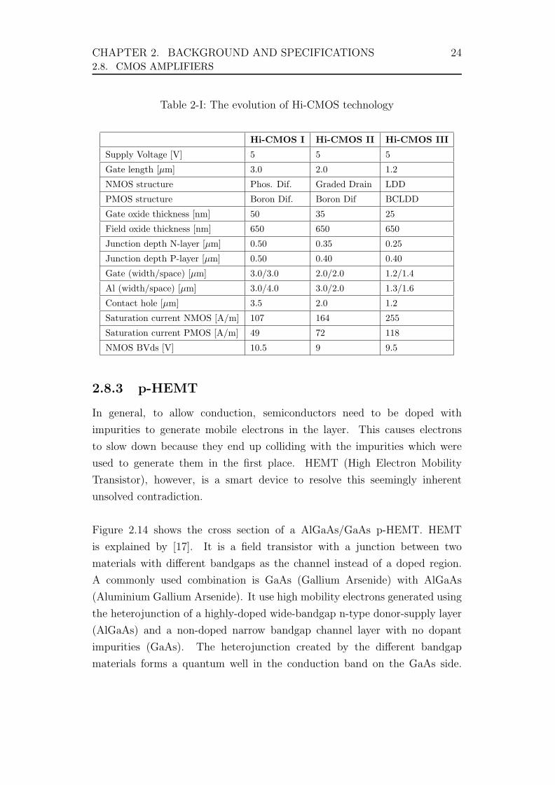
Figure 2.14 shows the cross section of a AlGaAs/GaAs p-HEMT. HEMT
is explained by [17]. It is a field transistor with a junction between two
materials with different bandgaps as the channel instead of a doped region.
A commonly used combination is GaAs (Gallium Arsenide) with AlGaAs
(Aluminium Gallium Arsenide). It use high mobility electrons generated using
the heterojunction of a highly-doped wide-bandgap n-type donor-supply layer
(AlGaAs) and a non-doped narrow bandgap channel layer with no dopant
impurities (GaAs). The heterojunction created by the different bandgap
materials forms a quantum well in the conduction band on the GaAs side.
CHAPTER 2. BACKGROUND AND SPECIFICATIONS 252.8. CMOS AMPLIFIERS
Source Gate Drainn+ GaAs
AlGaAs
Undoped GaAs
Semi-Insulating Substrate
Undoped AlGaAs SpacerInGaAs
Figure 2.14: Cross section of a AlGaAs/GaAs p-HEMT
That forces the electrons generated in the n-type AlGaAS thin layer to
drop completely into the GaAs layer to form a depletion AlGaAs layer. The
electrons can move fast in the GaAs side without colliding with any impurities
bacause the GaAs layer is undoped. That creates a very thin layer of highly
mobile conducting electrons , giving the channel very low resistivity and high
electron mobility. This layer is called a two-dimensional electron gas. As with
all other FET’s (Field-Effect Transistors), a voltage applied to the gate alters
the conductivity of the layer.
Ordinarily, the two different materials used for a heterojunction must
have the same lattice constant (spacing between the atoms). A p-HEMT
(pseudomorphic HEMT), however, has a different lattice constant for the two
different materials. This feat is achieved by using an extremely thin layer
InGaAs (Indium Gallium Arsenide). The layer is so thin that the crystal
lattice simply stretches to fit the other material. This technique allows the
construction of transistors with larger bandap differences than otherwise
possible for better performance.
Various hybrid amplifiers based on commercially available p-HEMT transistors
in a embedded microwave design were designed and characterised by [18].
They demonstrated the functionality of hybrid p-HEMT amplifiers for
CHAPTER 2. BACKGROUND AND SPECIFICATIONS 262.9. CRYOGENIC BEHAVIOUR OF RESISTORS AND CAPACITORS
cryogenic applications and successfully tested its digital operations at 4.2 K.
They achieved a total power consumption of less than 10 mW and a voltage
gain of about 30 dB at 4.2K.
2.9 Cryogenic behaviour of resistors and
capacitors
The complete amplifier should work at 4.2 K, therefore each component type
should be tested separately to confirm correct functionality at the specified
temperature.
Temperature
Figure 2.15: Tested resistor types with characteristic plots against cryogenictemperature range
Two types of resistors were tested by [19]. One is a radial carbon composition
resistor and the other a 0.25 watt Surface Mount Device (SMD) carbon film
resistor. Figure 2.15 shows their characteristics over a wide temperature
range, from 10 K to 300 K. From the graph it can be noted that the SMD
CHAPTER 2. BACKGROUND AND SPECIFICATIONS 272.9. CRYOGENIC BEHAVIOUR OF RESISTORS AND CAPACITORS
Figure 2.16: Tested capacitor types with characteristic plots against cryogenictemperature range
carbon film resistors had a 30 % increase in resistivity, while the radial
carbon composition resistors had an increase of 22 %. In this design the SMD
carbon film resistor is preferred above the radial carbon composition resistors
because it is manufactured in SMD package types which take up less space.
It is mainly used as feedback, gain and matching resistors, the change in the
resistivity can be incorporated into the design.
Figure 2.16 shows eight different types of capacitors that were tested by [19]
inside the cryocooler. Their results indicated that the polystyrene, polyester,
polycarbonate and tantalum capacitor types have an acceptable performance
with a less than 20 % deviance. The capacitors is mainly used as decoupling
capacitors that do not require precision capacitor values.
Chapter 3
Design Overview
This thesis consists of two parts. The first deals with the SCE, which consists
mainly of a Suzuki stack amplifier. It would amplify the power of each SFQ
pulse by increasing its amplitude and width. The SCE was not manufactured,
but simulation results are provided.
The second deals with the low temperature (4 K) behaviour of commercially
available CMOS amplifier IC’s. Section 3.2 shows the design of a test setup
used to characterise these amplifiers.
3.1 SCE Design Considerations
The SCE will only be simulated in WRSpice [20] and a circuit layout will be
done in Lasi 6. The Hypres design rules [21] were followed and a Monte Carlo
analysis was performed with Hypres manufacturing tolerances.
Any superconducting strip that connects two components has an inductance.
This inductance is very important in SCE’s [22]. Inductance in microstrip lines
cannot be described in terms of the line length alone. Different programs, such
as Lmeter [23], may be used to calculate inductances in the SCE structures.
28
CHAPTER 3. DESIGN OVERVIEW 293.1. SCE DESIGN CONSIDERATIONS
For the simulations, an inductance of at least 0.13 pH was used between all
the connections in the circuit. That would account for the inductance of the
superconducting strip connecting the components. A larger inductance was
used (calculated using Lmeter) for a longer connection.
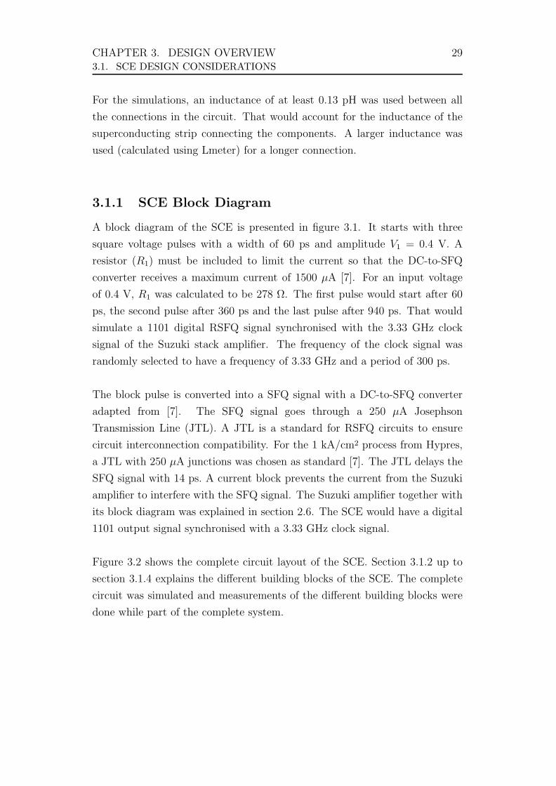
3.1.1 SCE Block Diagram
A block diagram of the SCE is presented in figure 3.1. It starts with three
square voltage pulses with a width of 60 ps and amplitude V1 = 0.4 V. A
resistor (R1) must be included to limit the current so that the DC-to-SFQ
converter receives a maximum current of 1500 µA [7]. For an input voltage
of 0.4 V, R1 was calculated to be 278 Ω. The first pulse would start after 60
ps, the second pulse after 360 ps and the last pulse after 940 ps. That would
simulate a 1101 digital RSFQ signal synchronised with the 3.33 GHz clock
signal of the Suzuki stack amplifier. The frequency of the clock signal was
randomly selected to have a frequency of 3.33 GHz and a period of 300 ps.
The block pulse is converted into a SFQ signal with a DC-to-SFQ converter
adapted from [7]. The SFQ signal goes through a 250 µA Josephson
Transmission Line (JTL). A JTL is a standard for RSFQ circuits to ensure
circuit interconnection compatibility. For the 1 kA/cm2 process from Hypres,
a JTL with 250 µA junctions was chosen as standard [7]. The JTL delays the
SFQ signal with 14 ps. A current block prevents the current from the Suzuki
amplifier to interfere with the SFQ signal. The Suzuki amplifier together with
its block diagram was explained in section 2.6. The SCE would have a digital
1101 output signal synchronised with a 3.33 GHz clock signal.
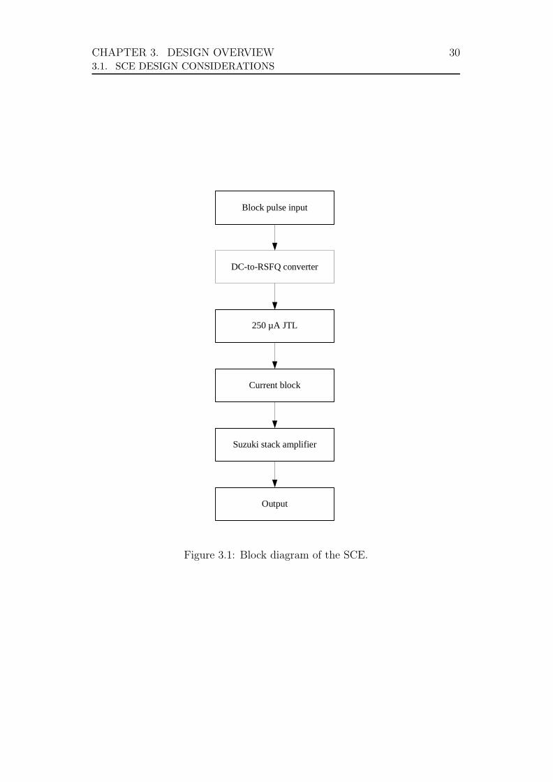
Figure 3.2 shows the complete circuit layout of the SCE. Section 3.1.2 up to
section 3.1.4 explains the different building blocks of the SCE. The complete
circuit was simulated and measurements of the different building blocks were
done while part of the complete system.
CHAPTER 3. DESIGN OVERVIEW 303.1. SCE DESIGN CONSIDERATIONS
Block pulse input
DC-to-RSFQ converter
250 µA JTL
Current block
Suzuki stack amplifier
Output
Figure 3.1: Block diagram of the SCE.
CHAPTER 3. DESIGN OVERVIEW 313.1. SCE DESIGN CONSIDERATIONS
V1
R1
R2
R3
R4
L 1 L 2
L 3
L 4
L 5L 6
L 7L 8
V2
R5
R6
L 9L 10 L 11
JJ1
JJ2 JJ
3JJ
4
L 12L 13
L 14L 15
L 16
R7
R8
R9
JJ5
JJ6
JJ7
V3
L 17 L 18L 19L 20L 21L 22L 23
L 24 L 25 L 26 JJ8
JJ9
JJ10
JJ11
JJ12
JJ13
JJ14
JJ15
R10
V4
R11
R12
DC
-to-R
SFQ
Con
verte
r25
0 µA
JTL
Curr
ent B
lock
Suzu
ki S
tack
Am
plifi
er
Figure 3.2: Full circuit layout of the SCE.
CHAPTER 3. DESIGN OVERVIEW 323.1. SCE DESIGN CONSIDERATIONS
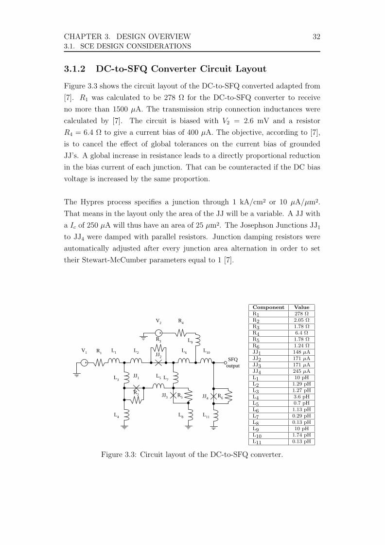
3.1.2 DC-to-SFQ Converter Circuit Layout
Figure 3.3 shows the circuit layout of the DC-to-SFQ converted adapted from
[7]. R1 was calculated to be 278 Ω for the DC-to-SFQ converter to receive
no more than 1500 µA. The transmission strip connection inductances were
calculated by [7]. The circuit is biased with V2 = 2.6 mV and a resistor
R4 = 6.4 Ω to give a current bias of 400 µA. The objective, according to [7],
is to cancel the effect of global tolerances on the current bias of grounded
JJ’s. A global increase in resistance leads to a directly proportional reduction
in the bias current of each junction. That can be counteracted if the DC bias
voltage is increased by the same proportion.
The Hypres process specifies a junction through 1 kA/cm2 or 10 µA/µm2.
That means in the layout only the area of the JJ will be a variable. A JJ with
a Ic of 250 µA will thus have an area of 25 µm2. The Josephson Junctions JJ1
to JJ4 were damped with parallel resistors. Junction damping resistors were
automatically adjusted after every junction area alternation in order to set
their Stewart-McCumber parameters equal to 1 [7].
V1 R1 L1 L2
L3
L4
R2
JJ1 L5
JJ2
R3
V2 R4
L6
L7
JJ3 R5
L8
L9
L10
JJ4 R6
L11
SFQoutput
Component ValueR1 278 ΩR2 2.05 ΩR3 1.78 ΩR4 6.4 ΩR5 1.78 ΩR6 1.24 ΩJJ1 148 µAJJ2 171 µAJJ3 171 µAJJ4 245 µAL1 10 pHL2 1.29 pHL3 1.27 pHL4 3.6 pHL5 0.7 pHL6 1.13 pHL7 0.29 pHL8 0.13 pHL9 10 pHL10 1.74 pHL11 0.13 pH
Figure 3.3: Circuit layout of the DC-to-SFQ converter.
CHAPTER 3. DESIGN OVERVIEW 333.1. SCE DESIGN CONSIDERATIONS
They used the equation
βc =2e
hIcR
2efC (3.1)
with
R−1ef = R−1
n + R−1s , (3.2)
where Rn is the normal resistance of the JJ and Rs the impedance of the
environment connected to the junction. For RSFQ βc = 1, e is the electron
charge, h is Planck’s constant, Ic the critical current of the junction and C
the capacitance.
Figure 3.4 shows the graph of the input and output current and voltage
of the DC-to-SFQ converter. Figure 3.2 on page 31 shows the complete
system. The input was measured as the signal delivered by V1 and the
output was measured before the inductor L12. The DC-to-SFQ converter
takes a rising edge and converts it into an SFQ signal. The converter
produces either a single SFQ pulse per period of the input block signal, or
two SFQ pulses per period depending on the amplitude of the block signal [24].
Due to the nature of SFQ pulses and the speed of conversion of a DC-to-SFQ
converter, input voltage pulses need only stay high for a few picoseconds [7].
CHAPTER 3. DESIGN OVERVIEW 343.1. SCE DESIGN CONSIDERATIONS
0 50 100 150-1000
-500
0
500
1000
1500
Time [ps]
Cur
rent
[μA
]
Input currentOutput current
(a) Input and output current against timegraph.
0 50 100 150-0.2
-0.1
0
0.1
0.2
0.3
0.4
0.5
Time [ps]
Vol
tage
Input voltage [V] Output voltage [mV]
(b) Input and output voltage against timegraph.
Figure 3.4: Time analysis of the input and output signals of the DC-to-SFQconverter.
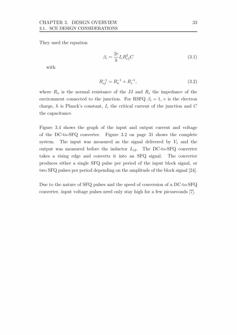
3.1.3 JTL250 Circuit Layout
Figure 3.5 shows the circuit layout of the 250 µA JTL [7]. The layout
structure was designed to have an inter-junction inductance of 4 pH. The
Josephson Junctions are damped with parallel resistors and the circuit is
biased with V3 = 2.6 mV and a resistor R9 = 15.6 Ω to provide a current bias
of 167 µA.
V3
R7
L12 L13 L14L15
R9JJ5 JJ6
R8
In Out
Component ValueR7 1.22 ΩR8 1.22 ΩR9 15.6 ΩL12 2 pHL13 2 pHL14 2 pHL15 2 pHJJ5 250 µAJJ6 250 µA
Figure 3.5: Circuit layout of the JTL250.
CHAPTER 3. DESIGN OVERVIEW 353.1. SCE DESIGN CONSIDERATIONS
The input and output of the JTL was measured while connected to the
complete system. Figure 3.2 on page 31 shows the JTL as part of the
complete system. The input was measured before the inductor, L12 and the
output was measured after the inductor, L15. Figure 3.6 shows the graph
of the input and output current and voltage through the 250 µA JTL. The
JTL decreases the total current of the SFQ pulse, but increases its voltage. It
gives the SFQ signal a delay of 16 ps.
0 50 100 150-400
-200
0
200
400
600
Time [ps]
Cur
rent
[μA
]
Input currentOutput current
(a) Input and output current against timegraph.
0 50 100 150
-200
-100
0
100
200
300
400
Time [ps]
Vol
tage
[μV
]
Input voltageOutput voltage
(b) Input and output voltage against timegraph.
Figure 3.6: Time analysis of the input and output signals of the 250 µA JTL.
3.1.4 Current Block
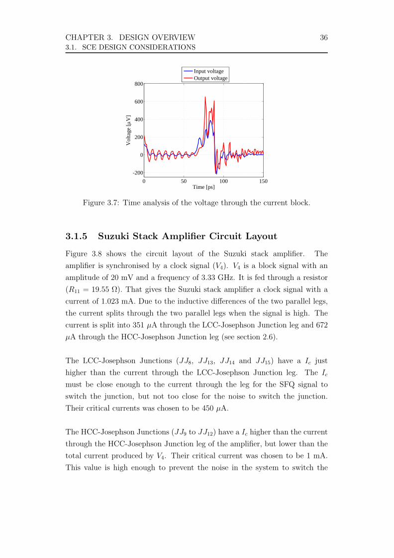
A Josephson Junction is used to prevent the current that drives the Suzuki
stack amplifier from interfering with the rest of the circuit. Figure 3.2 on page
31 shows the current block in the complete system. The Josephson Junction,
JJ7, has an Ic of 194 µA, which is damped with a parallel resistor R10 with
a resistance of 2 Ω. The Josephson Junction is connected in series with the
circuit, after the JTL before the input for the Suzuki stack amplifier, and
have no influence on the current. Figure 3.7 shows an increase, from 400 µV
to 600 µV, in the peak voltage of the SFQ signal.
CHAPTER 3. DESIGN OVERVIEW 363.1. SCE DESIGN CONSIDERATIONS
0 50 100 150-200
0
200
400
600
800
Time [ps]
Vol
tage
[μV
]
Input voltageOutput voltage
Figure 3.7: Time analysis of the voltage through the current block.
3.1.5 Suzuki Stack Amplifier Circuit Layout
Figure 3.8 shows the circuit layout of the Suzuki stack amplifier. The
amplifier is synchronised by a clock signal (V4). V4 is a block signal with an
amplitude of 20 mV and a frequency of 3.33 GHz. It is fed through a resistor
(R11 = 19.55 Ω). That gives the Suzuki stack amplifier a clock signal with a
current of 1.023 mA. Due to the inductive differences of the two parallel legs,
the current splits through the two parallel legs when the signal is high. The
current is split into 351 µA through the LCC-Josephson Junction leg and 672
µA through the HCC-Josephson Junction leg (see section 2.6).
The LCC-Josephson Junctions (JJ8, JJ13, JJ14 and JJ15) have a Ic just
higher than the current through the LCC-Josephson Junction leg. The Ic
must be close enough to the current through the leg for the SFQ signal to
switch the junction, but not too close for the noise to switch the junction.
Their critical currents was chosen to be 450 µA.
The HCC-Josephson Junctions (JJ9 to JJ12) have a Ic higher than the current
through the HCC-Josephson Junction leg of the amplifier, but lower than the
total current produced by V4. Their critical current was chosen to be 1 mA.
This value is high enough to prevent the noise in the system to switch the
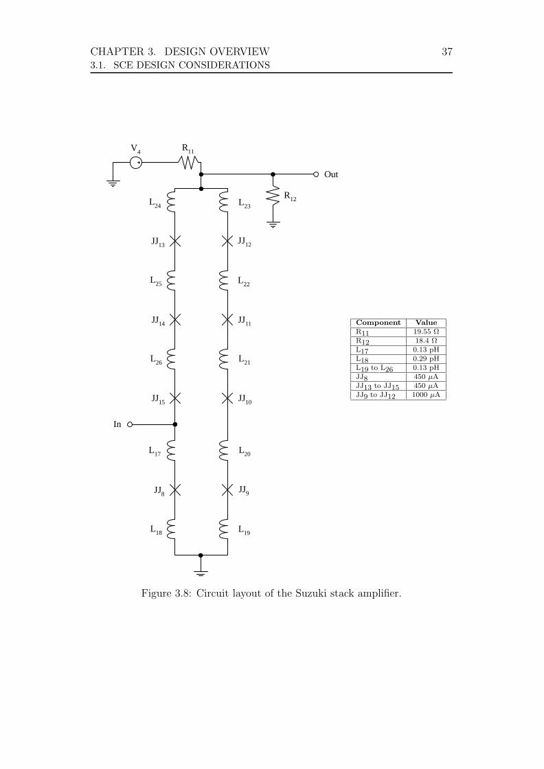
CHAPTER 3. DESIGN OVERVIEW 373.1. SCE DESIGN CONSIDERATIONS
V4 R11
L18 L19
L20
L21
R12
JJ8
L22
JJ9
L23L24
JJ10
L25
L26
L17
JJ11
JJ12JJ13
JJ14
JJ15
In
Out
Component ValueR11 19.55 ΩR12 18.4 ΩL17 0.13 pHL18 0.29 pHL19 to L26 0.13 pHJJ8 450 µAJJ13 to JJ15 450 µAJJ9 to JJ12 1000 µA
Figure 3.8: Circuit layout of the Suzuki stack amplifier.
CHAPTER 3. DESIGN OVERVIEW 383.1. SCE DESIGN CONSIDERATIONS
Josephson Junctions, but still lower than the total current delivered from the
external source.
The amplitude of the clock signal (V4) when it is high, much reach a value
of between 19.7 mV and 20.3 mV when it receives the SFQ signal. If the
amplitude of V4 is smaller than 18.5 mV, the SFQ signal will not switch the
input LCC-Josephson Junction (JJ8) to its resistive state. If V4 reach an
amplitude of more than 21.5 mV, the noise in the system will be enough to
switch JJ8.
The connections between the Josephson Junctions was simulated by inductors
with inductance of 0.13 pH. A larger inductance (L18 = 0.29 pH) was used
to give the inductive difference between the two parallel legs of the amplifier.
The output of the signal is delivered to a load resistor (R12 = 18.5 Ω).
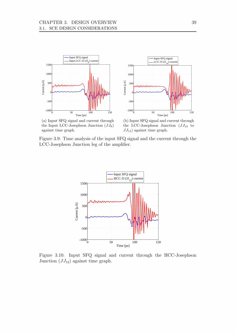
Figure 3.9 shows a graph of the current through the Suzuki stack amplifier
against time. For the graph, the clock signal at V4 is high. Figure 3.9a
shows the current through the input LCC-Josephson Junction (JJ8). As the
clock is high, the initial current through the junction is 351 µA. When the
SFQ signal is introduced into the Suzuki stack amplifier, the current through
JJ8 increases above its critical current (Ic = 450 µA). That switches JJ8
to its resistive state, and all the current delivered from V4 goes through the
HCC-Josephson Junction leg of the amplifier. Figure 3.9b shows that the
current through JJ13 drops as soon as the SFQ signal is introduced into the
circuit.
Figure 3.10 shows the current through the HCC-Josephson Junction (JJ12)
leg of the amplifier. When all the current delivered from V4 goes through
the HCC-Josephson Junction leg of the amplifier, the current through JJ12
increases above its critical current (Ic = 1 mA). That forces the junction to
switch to its resistive state, and the current delivered by V4 goes into the load
resistance (R12).
When JJ12 is switched to its resistive state, the output voltage will be the
CHAPTER 3. DESIGN OVERVIEW 393.1. SCE DESIGN CONSIDERATIONS
0 50 100 150-1000
-500
0
500
1000
1500
Time [ps]
Cur
rent
[μA
]
Input SFQ signalInput LCC-JJ (JJ8) current
(a) Input SFQ signal and current throughthe Input LCC-Josephson Junction (JJ8)against time graph.
0 50 100 150-1000
-500
0
500
1000
1500
Time [ps]
Cur
rent
[μA
]
Input SFQ signal LCC-JJ (JJ14) current
(b) Input SFQ signal and current throughthe LCC-Josephson Junction (JJ13 toJJ14) against time graph.
Figure 3.9: Time analysis of the input SFQ signal and the current through theLCC-Josephson Junction leg of the amplifier.
0 50 100 150-1000
-500
0
500
1000
1500
Time [ps]
Cur
rent
[μA
]
Input SFQ signal HCC-JJ (JJ12) current
Figure 3.10: Input SFQ signal and current through the HCC-JosephsonJunction (JJ12) against time graph.
CHAPTER 3. DESIGN OVERVIEW 403.1. SCE DESIGN CONSIDERATIONS
sum of the energy gaps across each Josephson Junction in the HCC-Josephson
Junction leg of the amplifier. The energy caps across each Josephson Junction
is just higher than 2 mV. Four HCC-Josephson Junctions in series would thus
result in an output voltage of 8.1 mV.
The junctions JJ8 and JJ12 will stay at their resistive states until the clock
(V4) drops to a low. That will decrease the current delivered and both
junctions will return to their superconducting states. When the clock switches
to high again, the delivered current will go through the Suzuki stack amplifier
to ground and the output current and voltage will remain at zero until the
next SFQ signal is received.
Figure 3.11 shows the input SFQ pulse and the output current of the Suzuki
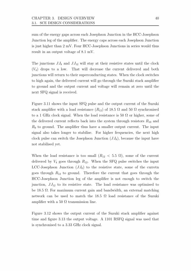
stack amplifier with a load resistance (R12) of 18.5 Ω and 50 Ω synchronised
to a 1 GHz clock signal. When the load resistance is 50 Ω or higher, some of
the delivered current reflects back into the system through resistors R10 and
R9 to ground. The amplifier thus have a smaller output current. The input
signal also takes longer to stabilise. For higher frequencies, the next high
clock pulse can switch the Josephson Junction (JJ8), because the input have
not stabilised yet.
When the load resistance is too small (R12 < 5.5 Ω), some of the current
delivered by V4 goes through R12. When the SFQ pulse switches the input
LCC-Josephson Junction (JJ8) to the resistive state, some of the curretn
goes through R12 to ground. Therefore the current that goes through the
HCC-Josephson Junction leg of the amplifier is not enough to switch the
junction, JJ12 to its resistive state. The load resistance was optimised to
be 18.5 Ω. For maximum current gain and bandwidth, an external matching
network can be used to match the 18.5 Ω load resistance of the Suzuki
amplifier with a 50 Ω transmission line.
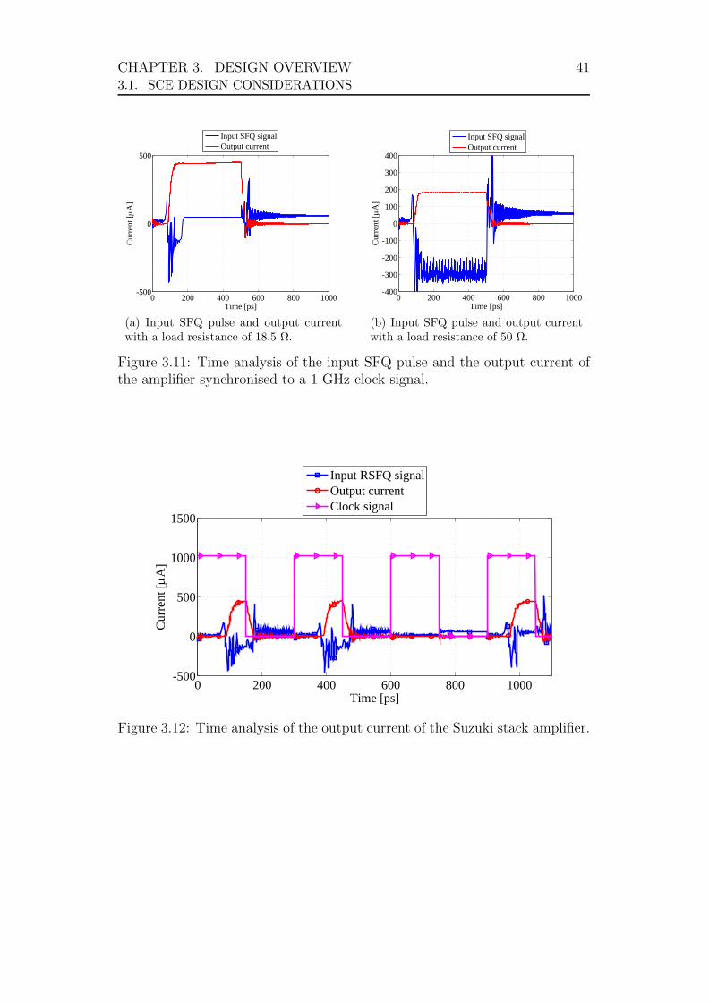
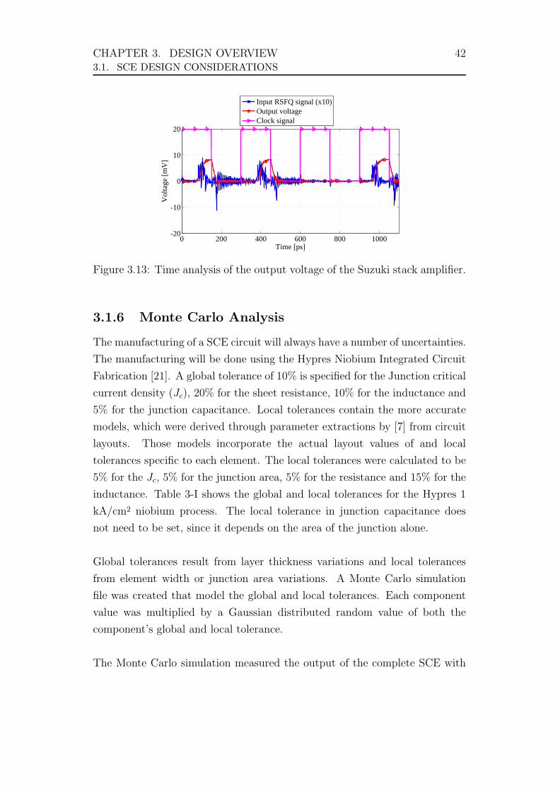
Figure 3.12 shows the output current of the Suzuki stack amplifier against
time and figure 3.13 the output voltage. A 1101 RSFQ signal was used that
is synchronised to a 3.33 GHz clock signal.
CHAPTER 3. DESIGN OVERVIEW 413.1. SCE DESIGN CONSIDERATIONS
0 200 400 600 800 1000-500
0
500
Time [ps]
Cur
rent
[μA
]
Input SFQ signalOutput current
(a) Input SFQ pulse and output currentwith a load resistance of 18.5 Ω.
0 200 400 600 800 1000-400
-300
-200
-100
0
100
200
300
400
Time [ps]
Cur
rent
[μA
]
Input SFQ signalOutput current
(b) Input SFQ pulse and output currentwith a load resistance of 50 Ω.
Figure 3.11: Time analysis of the input SFQ pulse and the output current ofthe amplifier synchronised to a 1 GHz clock signal.
0 200 400 600 800 1000-500
0
500
1000
1500
Time [ps]
Cur
rent
[μA
]
Input RSFQ signalOutput currentClock signal
Figure 3.12: Time analysis of the output current of the Suzuki stack amplifier.
CHAPTER 3. DESIGN OVERVIEW 423.1. SCE DESIGN CONSIDERATIONS
0 200 400 600 800 1000-20
-10
0
10
20
Time [ps]
Vol
tage
[mV
]
Input RSFQ signal (x10)Output voltageClock signal
Figure 3.13: Time analysis of the output voltage of the Suzuki stack amplifier.
3.1.6 Monte Carlo Analysis
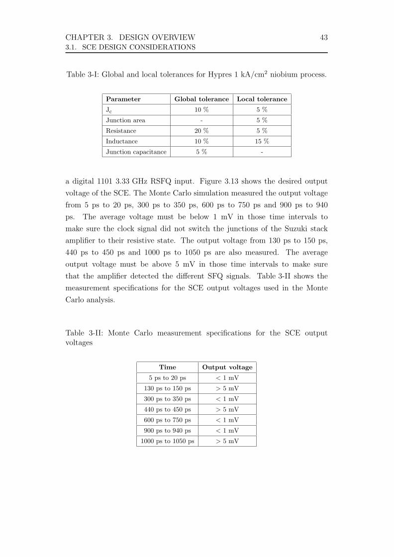
The manufacturing of a SCE circuit will always have a number of uncertainties.
The manufacturing will be done using the Hypres Niobium Integrated Circuit
Fabrication [21]. A global tolerance of 10% is specified for the Junction critical
current density (Jc), 20% for the sheet resistance, 10% for the inductance and
5% for the junction capacitance. Local tolerances contain the more accurate
models, which were derived through parameter extractions by [7] from circuit
layouts. Those models incorporate the actual layout values of and local
tolerances specific to each element. The local tolerances were calculated to be
5% for the Jc, 5% for the junction area, 5% for the resistance and 15% for the
inductance. Table 3-I shows the global and local tolerances for the Hypres 1
kA/cm2 niobium process. The local tolerance in junction capacitance does
not need to be set, since it depends on the area of the junction alone.
Global tolerances result from layer thickness variations and local tolerances
from element width or junction area variations. A Monte Carlo simulation
file was created that model the global and local tolerances. Each component
value was multiplied by a Gaussian distributed random value of both the
component’s global and local tolerance.
The Monte Carlo simulation measured the output of the complete SCE with
CHAPTER 3. DESIGN OVERVIEW 433.1. SCE DESIGN CONSIDERATIONS
Table 3-I: Global and local tolerances for Hypres 1 kA/cm2 niobium process.
Parameter Global tolerance Local tolerance
Jc 10 % 5 %
Junction area - 5 %
Resistance 20 % 5 %
Inductance 10 % 15 %
Junction capacitance 5 % -
a digital 1101 3.33 GHz RSFQ input. Figure 3.13 shows the desired output
voltage of the SCE. The Monte Carlo simulation measured the output voltage
from 5 ps to 20 ps, 300 ps to 350 ps, 600 ps to 750 ps and 900 ps to 940
ps. The average voltage must be below 1 mV in those time intervals to
make sure the clock signal did not switch the junctions of the Suzuki stack
amplifier to their resistive state. The output voltage from 130 ps to 150 ps,
440 ps to 450 ps and 1000 ps to 1050 ps are also measured. The average
output voltage must be above 5 mV in those time intervals to make sure
that the amplifier detected the different SFQ signals. Table 3-II shows the
measurement specifications for the SCE output voltages used in the Monte
Carlo analysis.
Table 3-II: Monte Carlo measurement specifications for the SCE outputvoltages
Time Output voltage
5 ps to 20 ps < 1 mV
130 ps to 150 ps > 5 mV
300 ps to 350 ps < 1 mV
440 ps to 450 ps > 5 mV
600 ps to 750 ps < 1 mV
900 ps to 940 ps < 1 mV
1000 ps to 1050 ps > 5 mV
CHAPTER 3. DESIGN OVERVIEW 443.1. SCE DESIGN CONSIDERATIONS
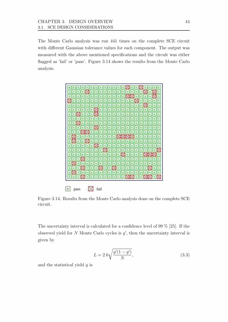
The Monte Carlo analysis was run 441 times on the complete SCE circuit
with different Gaussian tolerance values for each component. The output was
measured with the above mentioned specifications and the circuit was either
flagged as ’fail’ or ’pass’. Figure 3.14 shows the results from the Monte Carlo
analysis.
Fail failpassfailpass
Figure 3.14: Results from the Monte Carlo analysis done on the complete SCEcircuit.
The uncertainty interval is calculated for a confidence level of 99 % [25]. If the
observed yield for N Monte Carlo cycles is y′, then the uncertainty interval is
given by
L = 2.6
√y′(1− y′)
N, (3.3)
and the statistical yield y is
CHAPTER 3. DESIGN OVERVIEW 453.1. SCE DESIGN CONSIDERATIONS
y = y′ ± L. (3.4)
The Monte Carlo analysis predicts a yield of 89.9 %. From equation 3.3
and equation 3.4 the Monte Carlo analysis predicts a uncertainty interval
of 3.7 % and a statistical yield of 89.9 ± 3.7 %. However, the success of
the circuit is mainly related to the current received from the clock signal.
Either the initial current through the LCC-JJ leg of the Suzuki amplifier
was too high and the circuit amplified the clock signal, or it was too low
and the circuit couldn’t detect the SFQ signal. The current through the
Suzuki stack amplifier is controlled through an external source and can
be adjusted until the correct output is received. This enables circuits that
fail with normal inputs to be tuned during testing and improve the success rate.
3.1.7 SCE Layout
The layout of the circuit was done with Lasi 6. The Hypres process #03-10-45
design rules were used [21]. Square area Josephson Junctions were used
and the connections between the components were kept as small as possible.
The inductances between the connections were calculated with the sline.exe
program [26]. The layout key is shown in figure 3.15 [21]. Figure 3.16 shows
the Lasi 6 layout of the DC-to-SFQ converter, figure 3.17 the 250 µA JTL
and figure 3.18 the Suzuki stack amplifier. The JTL250 and the DC-to-SFQ
cells were created by [7]. Figure 3.19 shows the complete layout of the SCE
in Lasi 6. Figure 3.2 on page 31 shows the circuit schematic in WRSpice.
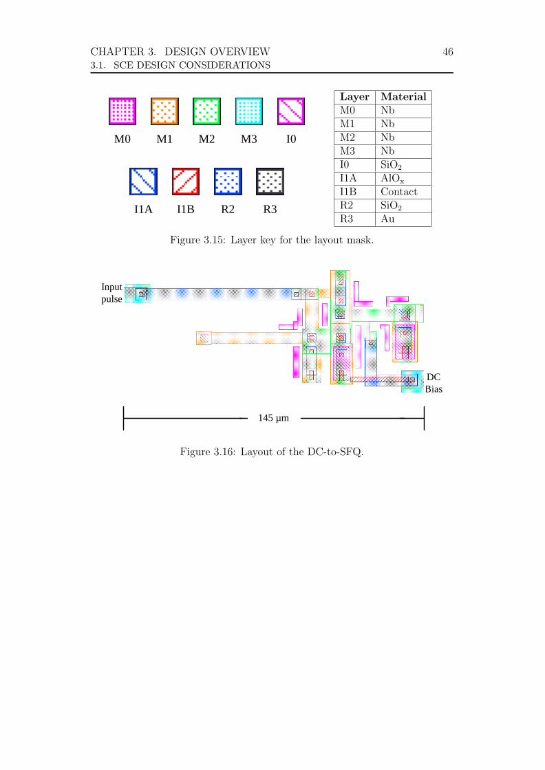
CHAPTER 3. DESIGN OVERVIEW 463.1. SCE DESIGN CONSIDERATIONS
M0 M1 M2 M3 I0
I1A I1B R2 R3
Layer MaterialM0 NbM1 NbM2 NbM3 NbI0 SiO2
I1A AlOx
I1B ContactR2 SiO2
R3 Au
Figure 3.15: Layer key for the layout mask.
DCBias
Inputpulse Output
SFQsignal
145 µm
Figure 3.16: Layout of the DC-to-SFQ.
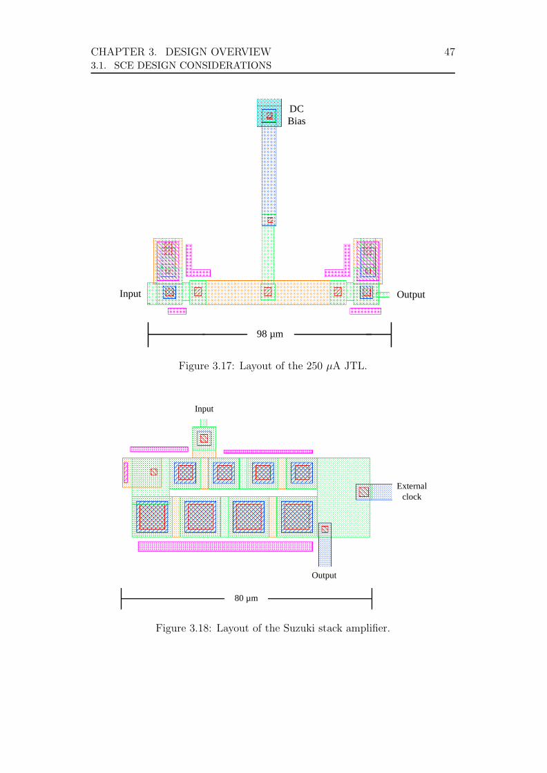
CHAPTER 3. DESIGN OVERVIEW 473.1. SCE DESIGN CONSIDERATIONS
DCBias
DCBias
Input Output
98 µm
Figure 3.17: Layout of the 250 µA JTL.
Input
Output
Externalclock
80 µm
Figure 3.18: Layout of the Suzuki stack amplifier.
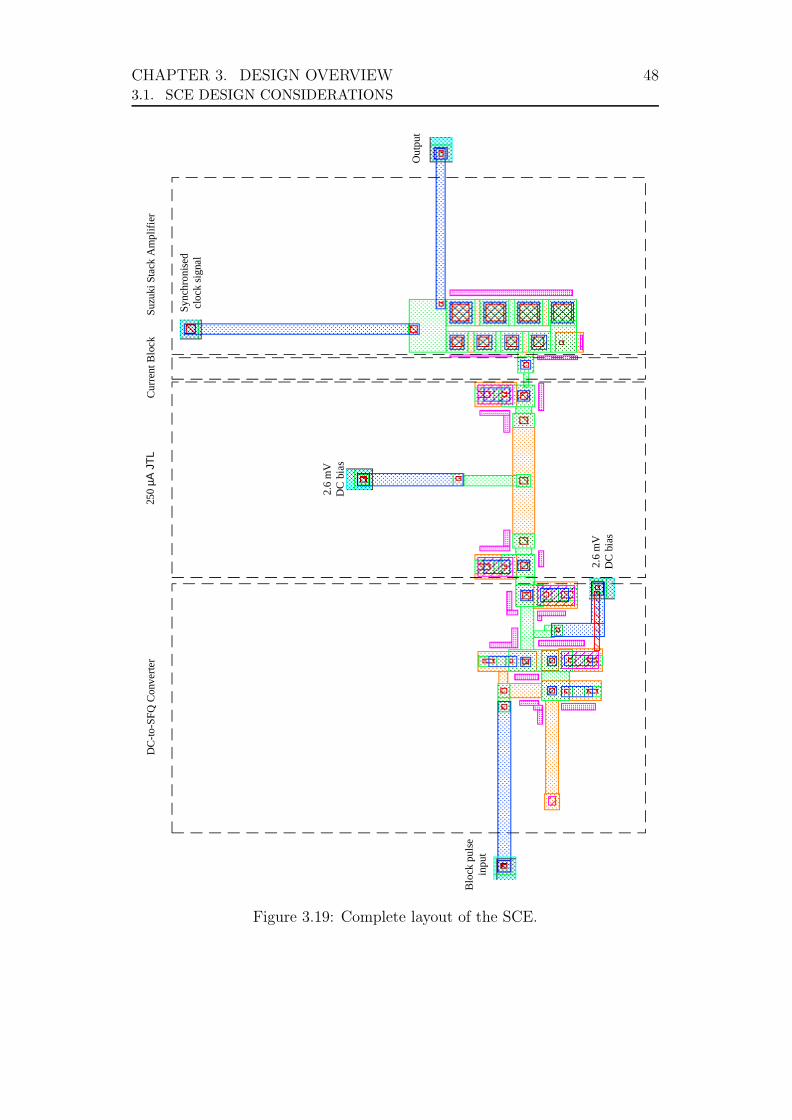
CHAPTER 3. DESIGN OVERVIEW 483.1. SCE DESIGN CONSIDERATIONS
DC
-to-S
FQ C
onve
rter
250
µA J
TLC
urre
nt B
lock
Suzu
ki S
tack
Am
plifi
er
Blo
ck p
ulse
inpu
t
2.6
mV
DC
bia
s
2.6
mV
DC
bia
s
Sync
hron
ised
cloc
k si
gnal
Out
put
Figure 3.19: Complete layout of the SCE.
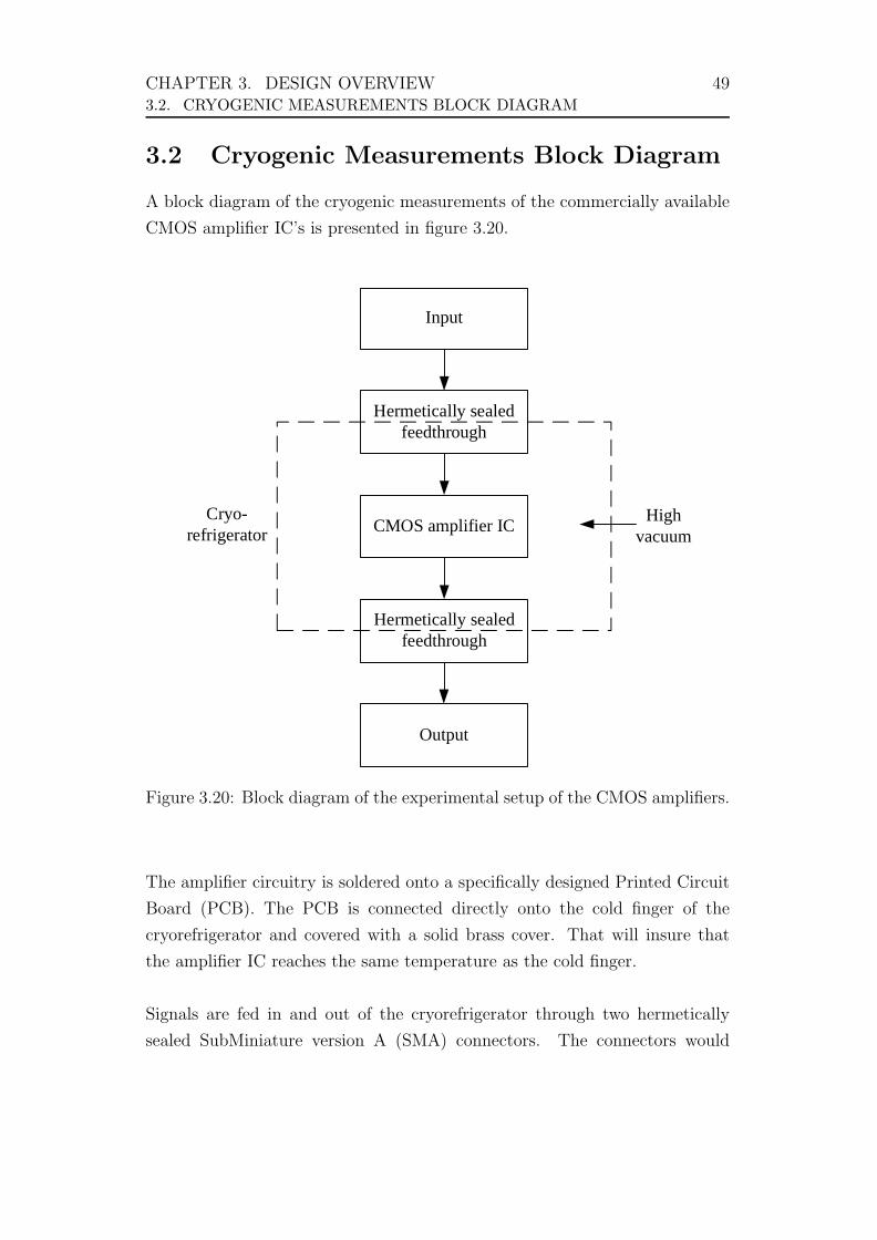
CHAPTER 3. DESIGN OVERVIEW 493.2. CRYOGENIC MEASUREMENTS BLOCK DIAGRAM
3.2 Cryogenic Measurements Block Diagram
A block diagram of the cryogenic measurements of the commercially available
CMOS amplifier IC’s is presented in figure 3.20.
Input
Hermetically sealedfeedthrough
CMOS amplifier IC
Hermetically sealedfeedthrough
Output
Cryo-refrigerator
Highvacuum
Figure 3.20: Block diagram of the experimental setup of the CMOS amplifiers.
The amplifier circuitry is soldered onto a specifically designed Printed Circuit
Board (PCB). The PCB is connected directly onto the cold finger of the
cryorefrigerator and covered with a solid brass cover. That will insure that
the amplifier IC reaches the same temperature as the cold finger.
Signals are fed in and out of the cryorefrigerator through two hermetically
sealed SubMiniature version A (SMA) connectors. The connectors would
CHAPTER 3. DESIGN OVERVIEW 503.2. CRYOGENIC MEASUREMENTS BLOCK DIAGRAM
allow access into the cryorefrigerator without breaking the vacuum required
within the cryorefrigerator. The measurement equipment are at room
temperature while the amplifier IC is cooled down to 4 K.
3.2.1 Cryogenic Measurements Setup
Ten commercially available CMOS amplifier IC’s was selected and tested in
the Cryorefrigerator. The PCB is designed to be 25.4mm × 25.4mm. As
explained in section 2.9, SMD film resistors are used. The resistors has a
uniform 30 % increase in resistivity at 4.2 K [8], but the smaller SMD package
types are required to fit all the components on the PCB. The resistors can be
designed to have the desired resistivity at 4.2 K.
Tantulum SMD capacitors were used when capacitances larger than 0.1 µF
was required, and Polystyrene Axial capacitors for smaller capacitances.
From section 2.9, one can see that the Tantalum SMD capacitors have a
less than 20 % decrease in capacitance at 4.2 K, while the Polystyrene Axial
capacitors have a 10 % increase at the same temperatures. The capacitors are
mainly used as DC-blocking and bypass capacitors, and a 20 % difference in
capacitance is acceptable.
The PCB’s were designed in Protel DXP and manufactured with FR4 PCB
material. The tracks are covered with a Tin (Sn) layer. The back plane of
the PCB is covered with the Sn layer, that acts as a solid ground layer. Each
individual amplifier circuit is placed in the centre of the PCB and surrounded
with a Sn layer that also acts as a ground.
A solid brass cover was designed and is illustrated in figure 3.21. The cover
has a width of 25 mm and a length of 35 mm. There is a square hole inside
the cover with a length and width of 22 mm and a depth of 10 mm. The
front of the hole is covered with two 23 SMA-50-0-1/111 NE female panel
connectors from Huber and Suhner. The PCB is screwed against the cold
finger of the cryorefrigerator with the brass cover. The amplifier components
fit inside the hole of the brass cover and the input and output of the amplifier
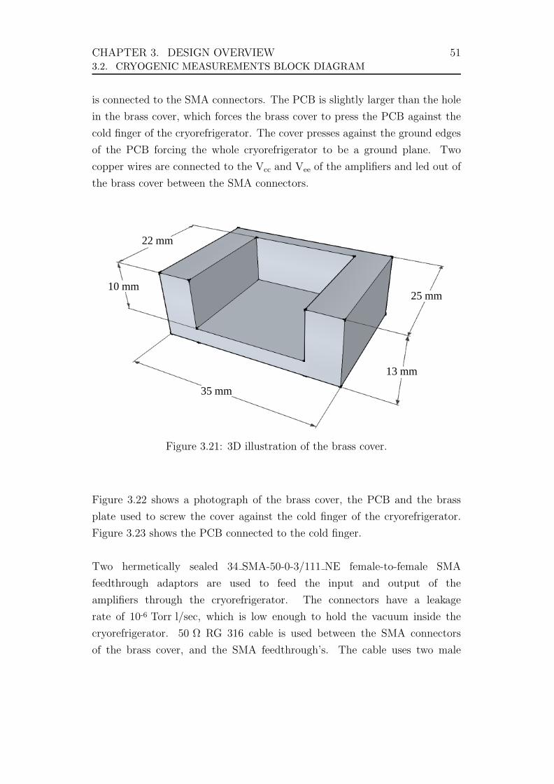
CHAPTER 3. DESIGN OVERVIEW 513.2. CRYOGENIC MEASUREMENTS BLOCK DIAGRAM
is connected to the SMA connectors. The PCB is slightly larger than the hole
in the brass cover, which forces the brass cover to press the PCB against the
cold finger of the cryorefrigerator. The cover presses against the ground edges
of the PCB forcing the whole cryorefrigerator to be a ground plane. Two
copper wires are connected to the Vcc and Vee of the amplifiers and led out of
the brass cover between the SMA connectors.
10 mm
13 mm
22 mm
25 mm
35 mm
Figure 3.21: 3D illustration of the brass cover.
Figure 3.22 shows a photograph of the brass cover, the PCB and the brass
plate used to screw the cover against the cold finger of the cryorefrigerator.
Figure 3.23 shows the PCB connected to the cold finger.
Two hermetically sealed 34 SMA-50-0-3/111 NE female-to-female SMA
feedthrough adaptors are used to feed the input and output of the
amplifiers through the cryorefrigerator. The connectors have a leakage
rate of 10-6 Torr l/sec, which is low enough to hold the vacuum inside the
cryorefrigerator. 50 Ω RG 316 cable is used between the SMA connectors
of the brass cover, and the SMA feedthrough’s. The cable uses two male
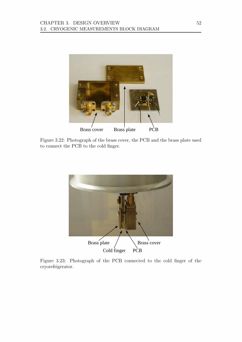
CHAPTER 3. DESIGN OVERVIEW 523.2. CRYOGENIC MEASUREMENTS BLOCK DIAGRAM
Brass cover PCBBrass plate
Figure 3.22: Photograph of the brass cover, the PCB and the brass plate usedto connect the PCB to the cold finger.
Brass coverBrass platePCBCold finger
Figure 3.23: Photograph of the PCB connected to the cold finger of thecryorefrigerator.
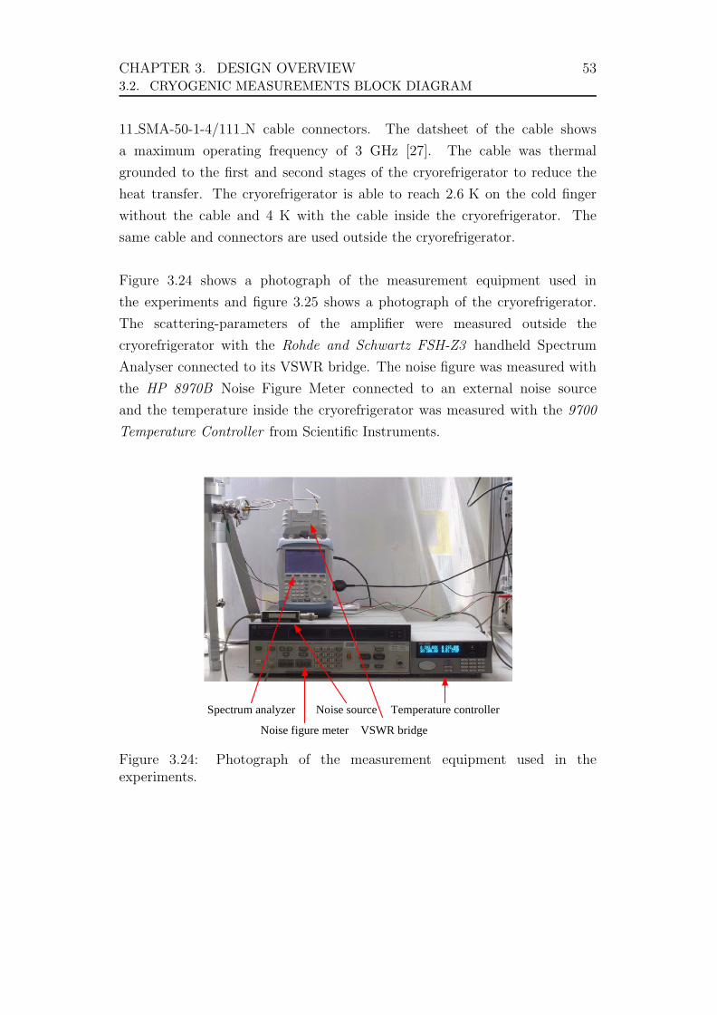
CHAPTER 3. DESIGN OVERVIEW 533.2. CRYOGENIC MEASUREMENTS BLOCK DIAGRAM
11 SMA-50-1-4/111 N cable connectors. The datsheet of the cable shows
a maximum operating frequency of 3 GHz [27]. The cable was thermal
grounded to the first and second stages of the cryorefrigerator to reduce the
heat transfer. The cryorefrigerator is able to reach 2.6 K on the cold finger
without the cable and 4 K with the cable inside the cryorefrigerator. The
same cable and connectors are used outside the cryorefrigerator.
Figure 3.24 shows a photograph of the measurement equipment used in
the experiments and figure 3.25 shows a photograph of the cryorefrigerator.
The scattering-parameters of the amplifier were measured outside the
cryorefrigerator with the Rohde and Schwartz FSH-Z3 handheld Spectrum
Analyser connected to its VSWR bridge. The noise figure was measured with
the HP 8970B Noise Figure Meter connected to an external noise source
and the temperature inside the cryorefrigerator was measured with the 9700
Temperature Controller from Scientific Instruments.
Spectrum analyzer
VSWR bridgeNoise figure meter
Temperature controllerNoise source
Figure 3.24: Photograph of the measurement equipment used in theexperiments.
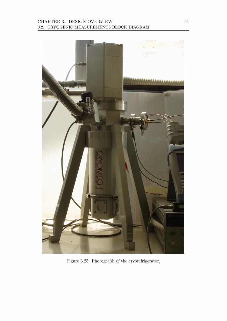
CHAPTER 3. DESIGN OVERVIEW 543.2. CRYOGENIC MEASUREMENTS BLOCK DIAGRAM
Figure 3.25: Photograph of the cryorefrigerator.
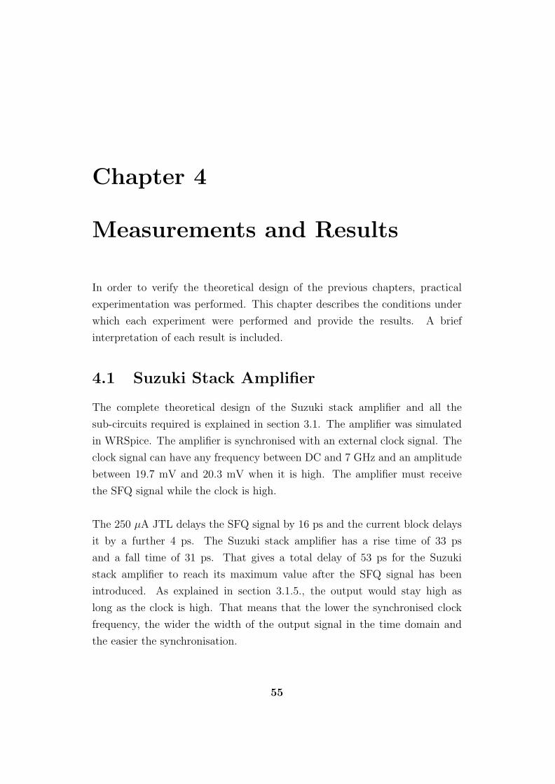
Chapter 4
Measurements and Results
In order to verify the theoretical design of the previous chapters, practical
experimentation was performed. This chapter describes the conditions under
which each experiment were performed and provide the results. A brief
interpretation of each result is included.
4.1 Suzuki Stack Amplifier
The complete theoretical design of the Suzuki stack amplifier and all the
sub-circuits required is explained in section 3.1. The amplifier was simulated
in WRSpice. The amplifier is synchronised with an external clock signal. The
clock signal can have any frequency between DC and 7 GHz and an amplitude
between 19.7 mV and 20.3 mV when it is high. The amplifier must receive
the SFQ signal while the clock is high.
The 250 µA JTL delays the SFQ signal by 16 ps and the current block delays
it by a further 4 ps. The Suzuki stack amplifier has a rise time of 33 ps
and a fall time of 31 ps. That gives a total delay of 53 ps for the Suzuki
stack amplifier to reach its maximum value after the SFQ signal has been
introduced. As explained in section 3.1.5., the output would stay high as
long as the clock is high. That means that the lower the synchronised clock
frequency, the wider the width of the output signal in the time domain and
the easier the synchronisation.
55
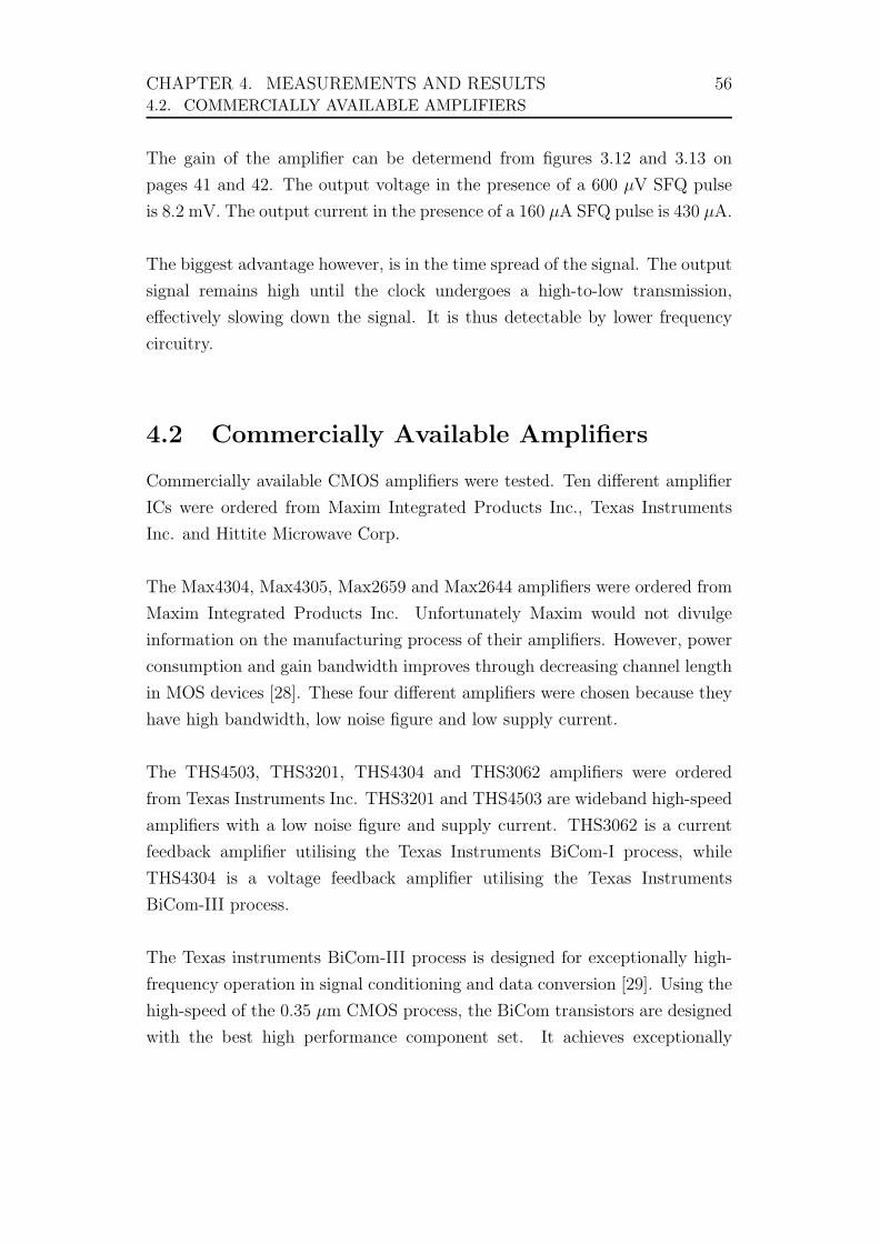
CHAPTER 4. MEASUREMENTS AND RESULTS 564.2. COMMERCIALLY AVAILABLE AMPLIFIERS
The gain of the amplifier can be determend from figures 3.12 and 3.13 on
pages 41 and 42. The output voltage in the presence of a 600 µV SFQ pulse
is 8.2 mV. The output current in the presence of a 160 µA SFQ pulse is 430 µA.
The biggest advantage however, is in the time spread of the signal. The output
signal remains high until the clock undergoes a high-to-low transmission,
effectively slowing down the signal. It is thus detectable by lower frequency
circuitry.
4.2 Commercially Available Amplifiers
Commercially available CMOS amplifiers were tested. Ten different amplifier
ICs were ordered from Maxim Integrated Products Inc., Texas Instruments
Inc. and Hittite Microwave Corp.
The Max4304, Max4305, Max2659 and Max2644 amplifiers were ordered from
Maxim Integrated Products Inc. Unfortunately Maxim would not divulge
information on the manufacturing process of their amplifiers. However, power
consumption and gain bandwidth improves through decreasing channel length
in MOS devices [28]. These four different amplifiers were chosen because they
have high bandwidth, low noise figure and low supply current.
The THS4503, THS3201, THS4304 and THS3062 amplifiers were ordered
from Texas Instruments Inc. THS3201 and THS4503 are wideband high-speed
amplifiers with a low noise figure and supply current. THS3062 is a current
feedback amplifier utilising the Texas Instruments BiCom-I process, while
THS4304 is a voltage feedback amplifier utilising the Texas Instruments
BiCom-III process.
The Texas instruments BiCom-III process is designed for exceptionally high-
frequency operation in signal conditioning and data conversion [29]. Using the
high-speed of the 0.35 µm CMOS process, the BiCom transistors are designed
with the best high performance component set. It achieves exceptionally
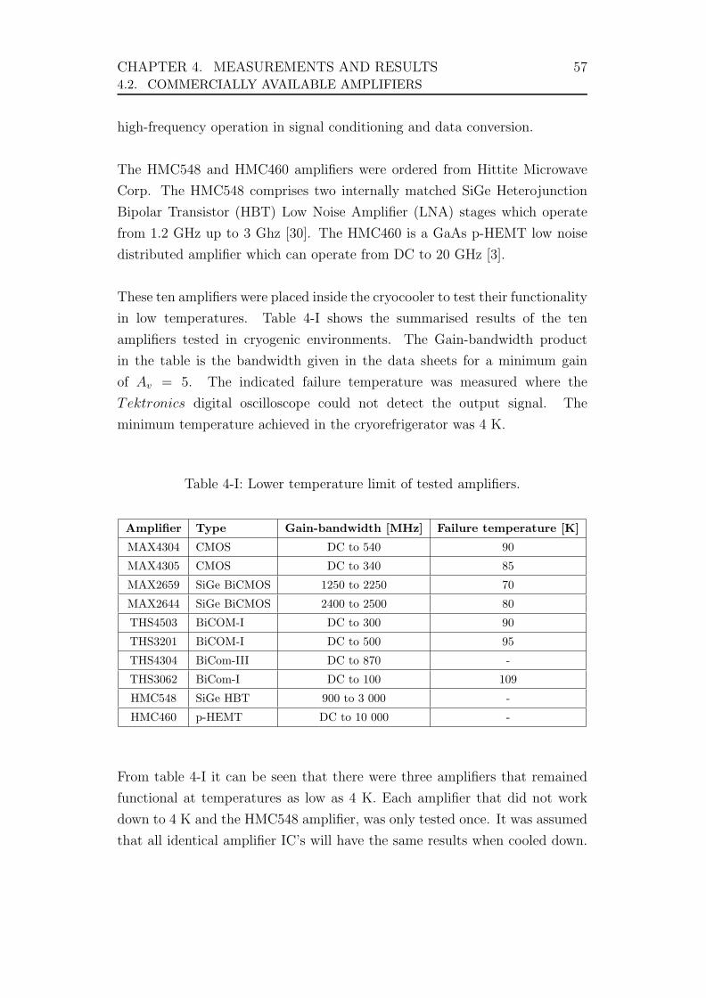
CHAPTER 4. MEASUREMENTS AND RESULTS 574.2. COMMERCIALLY AVAILABLE AMPLIFIERS
high-frequency operation in signal conditioning and data conversion.
The HMC548 and HMC460 amplifiers were ordered from Hittite Microwave
Corp. The HMC548 comprises two internally matched SiGe Heterojunction
Bipolar Transistor (HBT) Low Noise Amplifier (LNA) stages which operate
from 1.2 GHz up to 3 Ghz [30]. The HMC460 is a GaAs p-HEMT low noise
distributed amplifier which can operate from DC to 20 GHz [3].
These ten amplifiers were placed inside the cryocooler to test their functionality
in low temperatures. Table 4-I shows the summarised results of the ten
amplifiers tested in cryogenic environments. The Gain-bandwidth product
in the table is the bandwidth given in the data sheets for a minimum gain
of Av = 5. The indicated failure temperature was measured where the
Tektronics digital oscilloscope could not detect the output signal. The
minimum temperature achieved in the cryorefrigerator was 4 K.
Table 4-I: Lower temperature limit of tested amplifiers.
Amplifier Type Gain-bandwidth [MHz] Failure temperature [K]
MAX4304 CMOS DC to 540 90
MAX4305 CMOS DC to 340 85
MAX2659 SiGe BiCMOS 1250 to 2250 70
MAX2644 SiGe BiCMOS 2400 to 2500 80
THS4503 BiCOM-I DC to 300 90
THS3201 BiCOM-I DC to 500 95
THS4304 BiCom-III DC to 870 -
THS3062 BiCom-I DC to 100 109
HMC548 SiGe HBT 900 to 3 000 -
HMC460 p-HEMT DC to 10 000 -
From table 4-I it can be seen that there were three amplifiers that remained
functional at temperatures as low as 4 K. Each amplifier that did not work
down to 4 K and the HMC548 amplifier, was only tested once. It was assumed
that all identical amplifier IC’s will have the same results when cooled down.
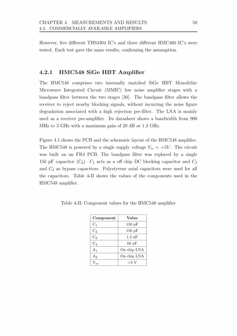
CHAPTER 4. MEASUREMENTS AND RESULTS 584.2. COMMERCIALLY AVAILABLE AMPLIFIERS
However, five different THS4304 IC’s and three different HMC460 IC’s were
tested. Each test gave the same results, confirming the assumption.
4.2.1 HMC548 SiGe HBT Amplifier
The HMC548 comprises two internally matched SiGe HBT Monolithic
Microwave Integrated Circuit (MMIC) low noise amplifier stages with a
bandpass filter between the two stages [30]. The bandpass filter allows the
receiver to reject nearby blocking signals, without incurring the noise figure
degradation associated with a high rejection pre-filter. The LNA is mainly
used as a receiver pre-amplifier. Its datasheet shows a bandwidth from 900
MHz to 3 GHz with a maximum gain of 20 dB at 1.3 GHz.
Figure 4.1 shows the PCB and the schematic layout of the HMC548 amplifier.
The HMC548 is powered by a single supply voltage Vcc = +5V . The circuit
was built on an FR4 PCB. The bandpass filter was replaced by a single
150 pF capacitor (C2). C1 acts as a off chip DC blocking capacitor and C3
and C4 as bypass capacitors. Polystyrene axial capacitors were used for all
the capacitors. Table 4-II shows the values of the components used in the
HMC548 amplifier.
Table 4-II: Component values for the HMC548 amplifier
Component Value
C1 150 pF
C2 150 pF
C3 1.2 nF
C4 68 nF
A1 On chip LNA
A2 On chip LNA
Vcc +5 V
CHAPTER 4. MEASUREMENTS AND RESULTS 594.2. COMMERCIALLY AVAILABLE AMPLIFIERS
C1
C2
C3
C4
In Out
Vcc
(a) PCB layout of the HMC548 amplifier.
In OutC1 C2
C3
C4
A1 A2
Vcc
(b) Schematic layout of the HMC548amplifier.
Figure 4.1: PCB and schematic layout of the HMC548 amplifier.
The frequency response of the amplifier was measured at room temperature
(300 K) and then again at 4 K. From the graph in figure 4.2 one can
see the temperature variations decreased the gain of the amplifier with a
maximum of 4 dB. The amplifier still showed a maximum gain of 20 dB at 4 K.
800 M 1 G 1.2 G 1.6 G 2.0 G 2.5 G-10
-5
0
5
10
15
20
25
Frequency [Hz]
Gai
n [d
B]
300 K4 K
Figure 4.2: Frequency response of the HMC548 amplifier at 300 K and 4 K
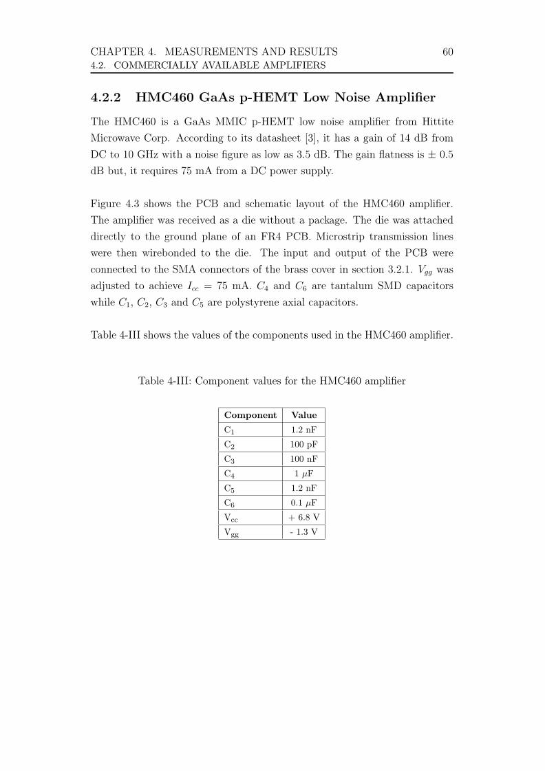
CHAPTER 4. MEASUREMENTS AND RESULTS 604.2. COMMERCIALLY AVAILABLE AMPLIFIERS
4.2.2 HMC460 GaAs p-HEMT Low Noise Amplifier
The HMC460 is a GaAs MMIC p-HEMT low noise amplifier from Hittite
Microwave Corp. According to its datasheet [3], it has a gain of 14 dB from
DC to 10 GHz with a noise figure as low as 3.5 dB. The gain flatness is ± 0.5
dB but, it requires 75 mA from a DC power supply.
Figure 4.3 shows the PCB and schematic layout of the HMC460 amplifier.
The amplifier was received as a die without a package. The die was attached
directly to the ground plane of an FR4 PCB. Microstrip transmission lines
were then wirebonded to the die. The input and output of the PCB were
connected to the SMA connectors of the brass cover in section 3.2.1. Vgg was
adjusted to achieve Icc = 75 mA. C4 and C6 are tantalum SMD capacitors
while C1, C2, C3 and C5 are polystyrene axial capacitors.
Table 4-III shows the values of the components used in the HMC460 amplifier.
Table 4-III: Component values for the HMC460 amplifier
Component Value
C1 1.2 nF
C2 100 pF
C3 100 nF
C4 1 µF
C5 1.2 nF
C6 0.1 µF
Vcc + 6.8 V
Vgg - 1.3 V
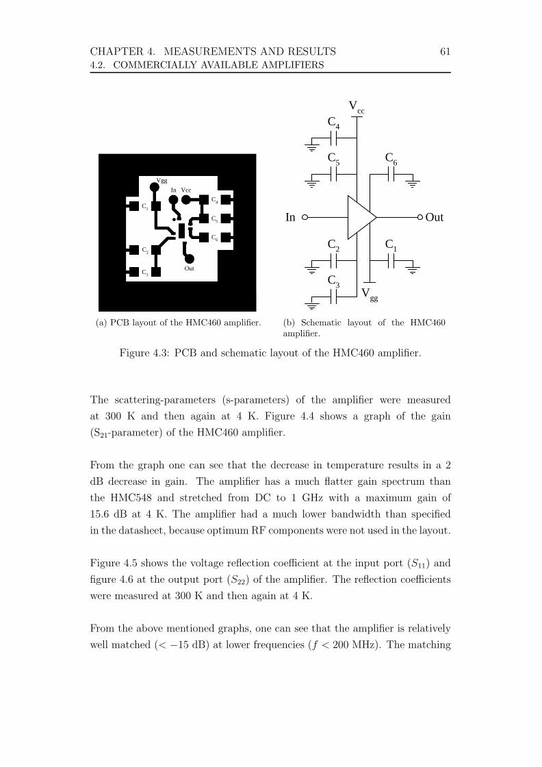
CHAPTER 4. MEASUREMENTS AND RESULTS 614.2. COMMERCIALLY AVAILABLE AMPLIFIERS
In
Out
VccVgg
C1
C2
C3
C4
C5
C6
(a) PCB layout of the HMC460 amplifier.
In Out
C1C2
C3
C4
C5 C6
Vcc
Vgg
(b) Schematic layout of the HMC460amplifier.
Figure 4.3: PCB and schematic layout of the HMC460 amplifier.
The scattering-parameters (s-parameters) of the amplifier were measured
at 300 K and then again at 4 K. Figure 4.4 shows a graph of the gain
(S21-parameter) of the HMC460 amplifier.
From the graph one can see that the decrease in temperature results in a 2
dB decrease in gain. The amplifier has a much flatter gain spectrum than
the HMC548 and stretched from DC to 1 GHz with a maximum gain of
15.6 dB at 4 K. The amplifier had a much lower bandwidth than specified
in the datasheet, because optimum RF components were not used in the layout.
Figure 4.5 shows the voltage reflection coefficient at the input port (S11) and
figure 4.6 at the output port (S22) of the amplifier. The reflection coefficients
were measured at 300 K and then again at 4 K.
From the above mentioned graphs, one can see that the amplifier is relatively
well matched (< −15 dB) at lower frequencies (f < 200 MHz). The matching
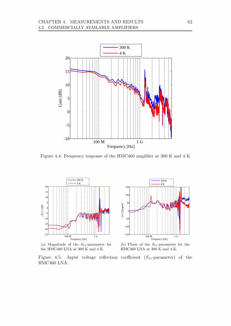
CHAPTER 4. MEASUREMENTS AND RESULTS 624.2. COMMERCIALLY AVAILABLE AMPLIFIERS
100 M 1 G-10
-5
0
5
10
15
20
Frequency [Hz]
Gai
n [d
B]
300 K4 K
Figure 4.4: Frequency response of the HMC460 amplifier at 300 K and 4 K
100 M 1 G-25
-20
-15
-10
-5
0
5
10
15
20
Frequency [Hz]
| S11
| [d
B]
300 K4 K
(a) Magnitude of the S11-parameter forthe HMC460 LNA at 300 K and 4 K.
100 M 1 G-150
-100
-50
0
50
100
150
Frequency [Hz]
< S1
1 [D
egre
e]
300 K4 K
(b) Phase of the S11-parameter for theHMC460 LNA at 300 K and 4 K.
Figure 4.5: Input voltage reflection coefficient (S11-parameter) of theHMC460 LNA.
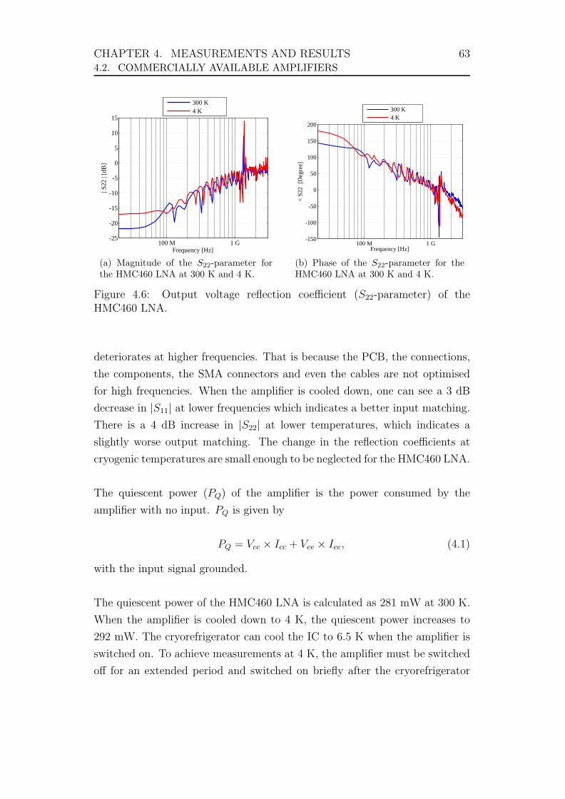
CHAPTER 4. MEASUREMENTS AND RESULTS 634.2. COMMERCIALLY AVAILABLE AMPLIFIERS
100 M 1 G-25
-20
-15
-10
-5
0
5
10
15
Frequency [Hz]
| S22
| [d
B]
300 K4 K
(a) Magnitude of the S22-parameter forthe HMC460 LNA at 300 K and 4 K.
100 M 1 G-150
-100
-50
0
50
100
150
200
Frequency [Hz]
< S2
2 [D
egre
e]
300 K4 K
(b) Phase of the S22-parameter for theHMC460 LNA at 300 K and 4 K.
Figure 4.6: Output voltage reflection coefficient (S22-parameter) of theHMC460 LNA.
deteriorates at higher frequencies. That is because the PCB, the connections,
the components, the SMA connectors and even the cables are not optimised
for high frequencies. When the amplifier is cooled down, one can see a 3 dB
decrease in |S11| at lower frequencies which indicates a better input matching.
There is a 4 dB increase in |S22| at lower temperatures, which indicates a
slightly worse output matching. The change in the reflection coefficients at
cryogenic temperatures are small enough to be neglected for the HMC460 LNA.
The quiescent power (PQ) of the amplifier is the power consumed by the
amplifier with no input. PQ is given by
PQ = Vcc × Icc + Vee × Iee, (4.1)
with the input signal grounded.
The quiescent power of the HMC460 LNA is calculated as 281 mW at 300 K.
When the amplifier is cooled down to 4 K, the quiescent power increases to
292 mW. The cryorefrigerator can cool the IC to 6.5 K when the amplifier is
switched on. To achieve measurements at 4 K, the amplifier must be switched
off for an extended period and switched on briefly after the cryorefrigerator
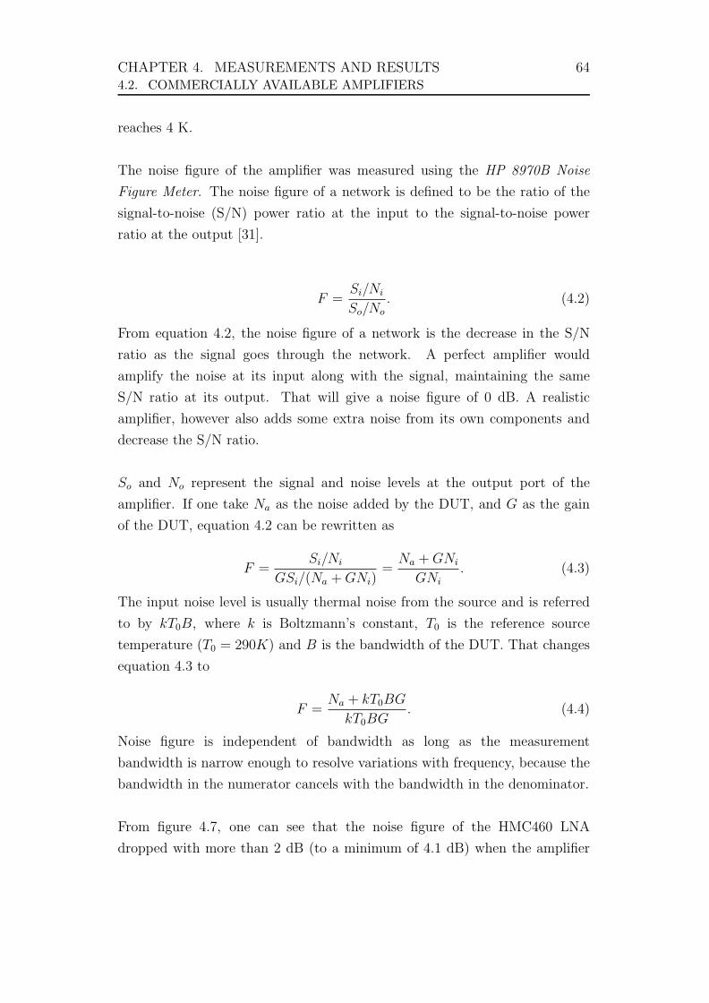
CHAPTER 4. MEASUREMENTS AND RESULTS 644.2. COMMERCIALLY AVAILABLE AMPLIFIERS
reaches 4 K.
The noise figure of the amplifier was measured using the HP 8970B Noise
Figure Meter. The noise figure of a network is defined to be the ratio of the
signal-to-noise (S/N) power ratio at the input to the signal-to-noise power
ratio at the output [31].
F =Si/Ni
So/No
. (4.2)
From equation 4.2, the noise figure of a network is the decrease in the S/N
ratio as the signal goes through the network. A perfect amplifier would
amplify the noise at its input along with the signal, maintaining the same
S/N ratio at its output. That will give a noise figure of 0 dB. A realistic
amplifier, however also adds some extra noise from its own components and
decrease the S/N ratio.
So and No represent the signal and noise levels at the output port of the
amplifier. If one take Na as the noise added by the DUT, and G as the gain
of the DUT, equation 4.2 can be rewritten as
F =Si/Ni
GSi/(Na + GNi)=
Na + GNi
GNi
. (4.3)
The input noise level is usually thermal noise from the source and is referred
to by kT0B, where k is Boltzmann’s constant, T0 is the reference source
temperature (T0 = 290K) and B is the bandwidth of the DUT. That changes
equation 4.3 to
F =Na + kT0BG
kT0BG. (4.4)
Noise figure is independent of bandwidth as long as the measurement
bandwidth is narrow enough to resolve variations with frequency, because the
bandwidth in the numerator cancels with the bandwidth in the denominator.
From figure 4.7, one can see that the noise figure of the HMC460 LNA
dropped with more than 2 dB (to a minimum of 4.1 dB) when the amplifier
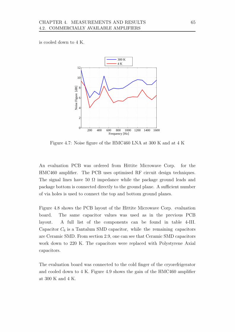
CHAPTER 4. MEASUREMENTS AND RESULTS 654.2. COMMERCIALLY AVAILABLE AMPLIFIERS
is cooled down to 4 K.
200 400 600 800 1000 1200 1400 16000
2
4
6
8
10
12
Frequency [Hz]
Noi
se F
igur
e [d
B]
300 K4 K
Figure 4.7: Noise figure of the HMC460 LNA at 300 K and at 4 K
An evaluation PCB was ordered from Hittite Microwave Corp. for the
HMC460 amplifier. The PCB uses optimised RF circuit design techniques.
The signal lines have 50 Ω impedance while the package ground leads and
package bottom is connected directly to the ground plane. A sufficient number
of via holes is used to connect the top and bottom ground planes.
Figure 4.8 shows the PCB layout of the Hittite Microwave Corp. evaluation
board. The same capacitor values was used as in the previous PCB
layout. A full list of the components can be found in table 4-III.
Capacitor C6 is a Tantalum SMD capacitor, while the remaining capacitors
are Ceramic SMD. From section 2.9, one can see that Ceramic SMD capacitors
work down to 220 K. The capacitors were replaced with Polystyrene Axial
capacitors.
The evaluation board was connected to the cold finger of the cryorefrigerator
and cooled down to 4 K. Figure 4.9 shows the gain of the HMC460 amplifier
at 300 K and 4 K.
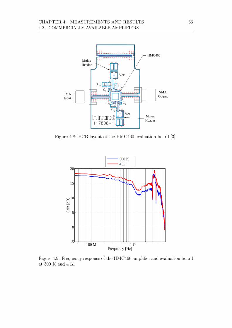
CHAPTER 4. MEASUREMENTS AND RESULTS 664.2. COMMERCIALLY AVAILABLE AMPLIFIERS
In
Out
VccVee
C1
C2
C3
C4
C5
C6
Vee
Vcc
SMAInput
SMAOutput
HMC460
C1C2
C3
C4C5
C6
MolexHeader
MolexHeader
Figure 4.8: PCB layout of the HMC460 evaluation board [3].
100 M 1 G-5
0
5
10
15
20
Frequency [Hz]
Gai
n [d
B]
300 K4 K
Figure 4.9: Frequency response of the HMC460 amplifier and evaluation boardat 300 K and 4 K.
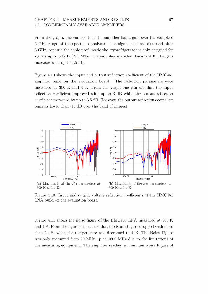
CHAPTER 4. MEASUREMENTS AND RESULTS 674.2. COMMERCIALLY AVAILABLE AMPLIFIERS
From the graph, one can see that the amplifier has a gain over the complete
6 GHz range of the spectrum analyser. The signal becomes distorted after
3 GHz, because the cable used inside the cryorefrigerator is only designed for
signals up to 3 GHz [27]. When the amplifier is cooled down to 4 K, the gain
increases with up to 1.5 dB.
Figure 4.10 shows the input and output reflection coefficient of the HMC460
amplifier build on the evaluation board. The reflection parameters were
measured at 300 K and 4 K. From the graph one can see that the input
reflection coefficient improved with up to 3 dB while the output reflection
coefficient worsened by up to 3.5 dB. However, the output reflection coefficient
remains lower than -15 dB over the band of interest.
100 M 1 G-40
-35
-30
-25
-20
-15
-10
-5
0
Frequency [Hz]
| S11
| [d
B]
300 K4 K
(a) Magnitude of the S11-parameters at300 K and 4 K.
100 M 1 G-40
-35
-30
-25
-20
-15
-10
-5
0
Frequency [Hz]
| S22
| [d
B]
300 K4 K
(b) Magnitude of the S22-parameters at300 K and 4 K.
Figure 4.10: Input and output voltage reflection coefficients of the HMC460LNA build on the evaluation board.
Figure 4.11 shows the noise figure of the HMC460 LNA measured at 300 K
and 4 K. From the figure one can see that the Noise Figure dropped with more
than 2 dB, when the temperature was decreased to 4 K. The Noise Figure
was only measured from 20 MHz up to 1600 MHz due to the limitations of
the measuring equipment. The amplifier reached a minimum Noise Figure of
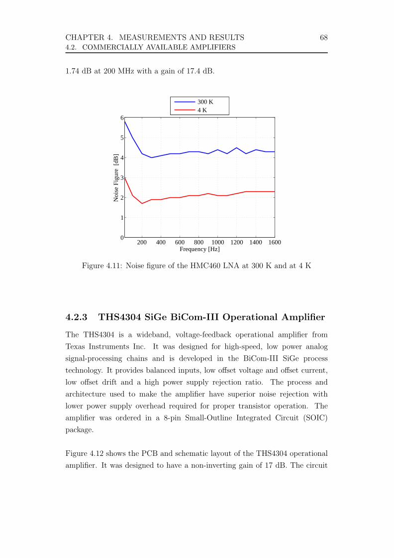
CHAPTER 4. MEASUREMENTS AND RESULTS 684.2. COMMERCIALLY AVAILABLE AMPLIFIERS
1.74 dB at 200 MHz with a gain of 17.4 dB.
200 400 600 800 1000 1200 1400 16000
1
2
3
4
5
6
Frequency [Hz]
Noi
se F
igur
e [d
B]
300 K4 K
Figure 4.11: Noise figure of the HMC460 LNA at 300 K and at 4 K
4.2.3 THS4304 SiGe BiCom-III Operational Amplifier
The THS4304 is a wideband, voltage-feedback operational amplifier from
Texas Instruments Inc. It was designed for high-speed, low power analog
signal-processing chains and is developed in the BiCom-III SiGe process
technology. It provides balanced inputs, low offset voltage and offset current,
low offset drift and a high power supply rejection ratio. The process and
architecture used to make the amplifier have superior noise rejection with
lower power supply overhead required for proper transistor operation. The
amplifier was ordered in a 8-pin Small-Outline Integrated Circuit (SOIC)
package.
Figure 4.12 shows the PCB and schematic layout of the THS4304 operational
amplifier. It was designed to have a non-inverting gain of 17 dB. The circuit
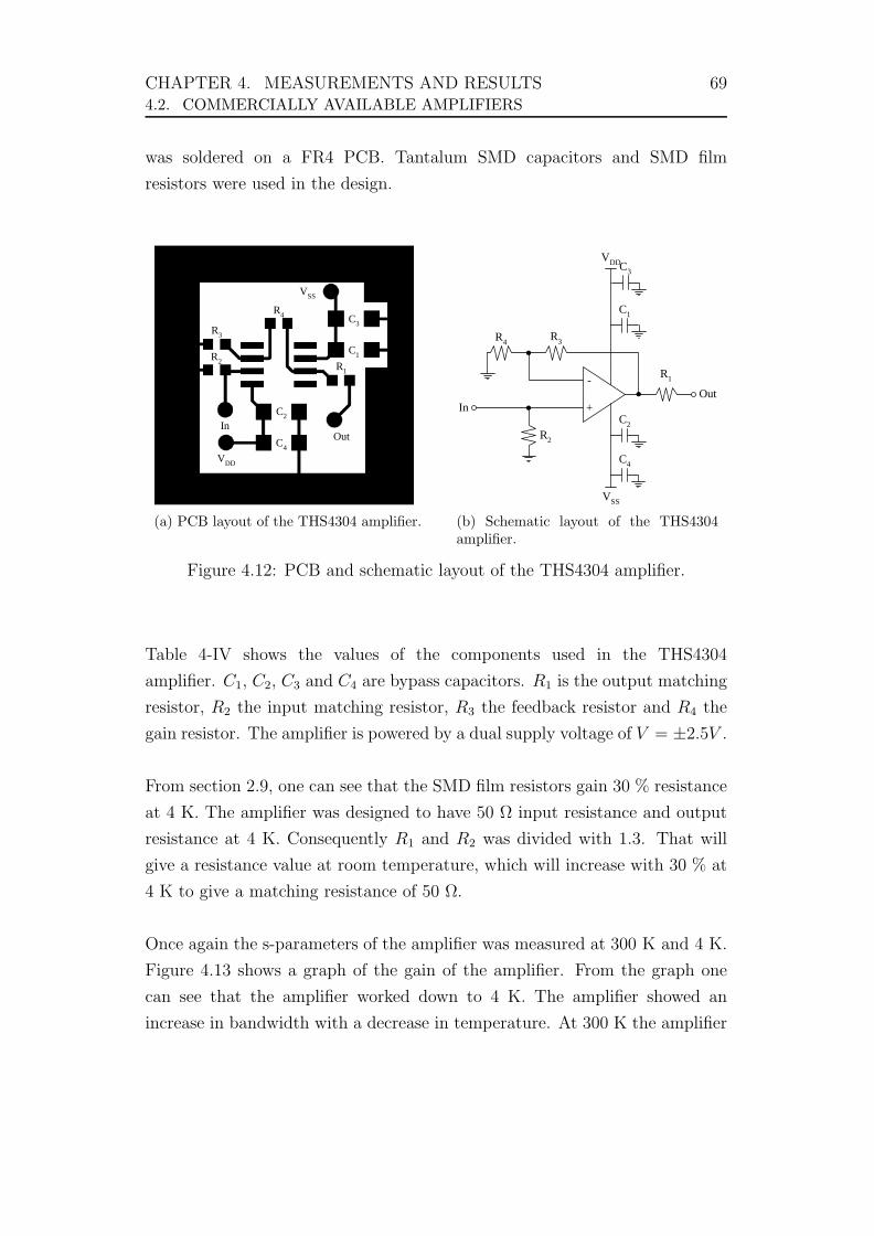
CHAPTER 4. MEASUREMENTS AND RESULTS 694.2. COMMERCIALLY AVAILABLE AMPLIFIERS
was soldered on a FR4 PCB. Tantalum SMD capacitors and SMD film
resistors were used in the design.
R1
R3
R2
R4
C1
C2
C3
C4
InOut
VDD
VSS
(a) PCB layout of the THS4304 amplifier.
+
-
InOut
R1
R2
R3R4
C1
C3
C2
VDD
VSS
C4
(b) Schematic layout of the THS4304amplifier.
Figure 4.12: PCB and schematic layout of the THS4304 amplifier.
Table 4-IV shows the values of the components used in the THS4304
amplifier. C1, C2, C3 and C4 are bypass capacitors. R1 is the output matching
resistor, R2 the input matching resistor, R3 the feedback resistor and R4 the
gain resistor. The amplifier is powered by a dual supply voltage of V = ±2.5V .
From section 2.9, one can see that the SMD film resistors gain 30 % resistance
at 4 K. The amplifier was designed to have 50 Ω input resistance and output
resistance at 4 K. Consequently R1 and R2 was divided with 1.3. That will
give a resistance value at room temperature, which will increase with 30 % at
4 K to give a matching resistance of 50 Ω.
Once again the s-parameters of the amplifier was measured at 300 K and 4 K.
Figure 4.13 shows a graph of the gain of the amplifier. From the graph one
can see that the amplifier worked down to 4 K. The amplifier showed an
increase in bandwidth with a decrease in temperature. At 300 K the amplifier
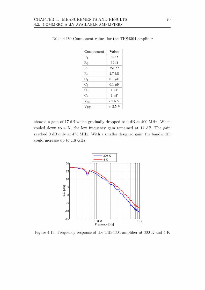
CHAPTER 4. MEASUREMENTS AND RESULTS 704.2. COMMERCIALLY AVAILABLE AMPLIFIERS
Table 4-IV: Component values for the THS4304 amplifier
Component Value
R1 39 Ω
R2 39 Ω
R3 270 Ω
R4 2.7 kΩ
C1 0.1 µF
C2 0.1 µF
C3 1 µF
C4 1 µF
VSS - 2.5 V
VDD + 2.5 V
showed a gain of 17 dB which gradually dropped to 0 dB at 400 MHz. When
cooled down to 4 K, the low frequency gain remained at 17 dB. The gain
reached 0 dB only at 475 MHz. With a smaller designed gain, the bandwidth
could increase up to 1.8 GHz.
100 M 1 G-15
-10
-5
0
5
10
15
20
Frequency [Hz]
Gai
n [d
B]
300 K4 K
Figure 4.13: Frequency response of the THS4304 amplifier at 300 K and 4 K
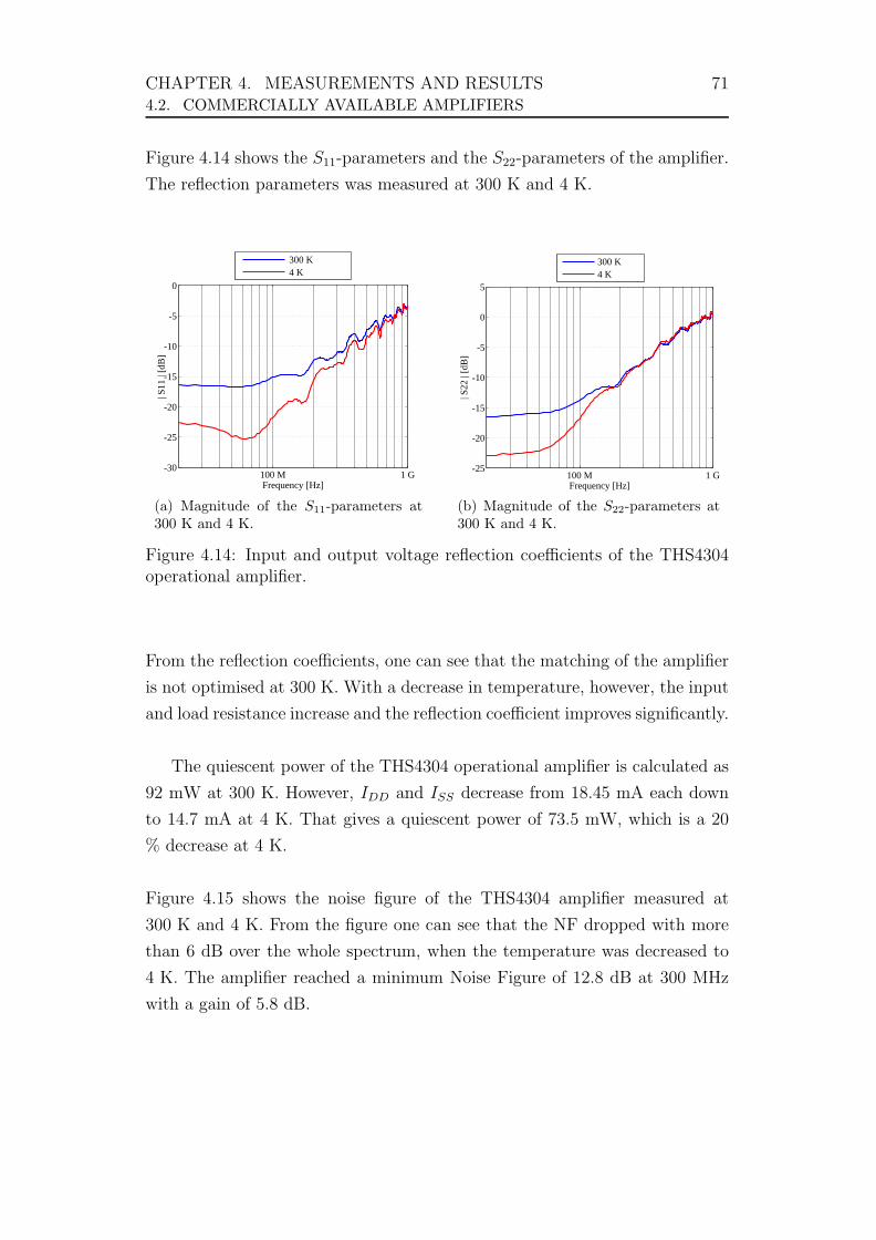
CHAPTER 4. MEASUREMENTS AND RESULTS 714.2. COMMERCIALLY AVAILABLE AMPLIFIERS
Figure 4.14 shows the S11-parameters and the S22-parameters of the amplifier.
The reflection parameters was measured at 300 K and 4 K.
100 M 1 G-30
-25
-20
-15
-10
-5
0
Frequency [Hz]
| S11
| [d
B]
300 K4 K
(a) Magnitude of the S11-parameters at300 K and 4 K.
100 M 1 G-25
-20
-15
-10
-5
0
5
Frequency [Hz]
| S22
| [d
B]
300 K4 K
(b) Magnitude of the S22-parameters at300 K and 4 K.
Figure 4.14: Input and output voltage reflection coefficients of the THS4304operational amplifier.
From the reflection coefficients, one can see that the matching of the amplifier
is not optimised at 300 K. With a decrease in temperature, however, the input
and load resistance increase and the reflection coefficient improves significantly.
The quiescent power of the THS4304 operational amplifier is calculated as
92 mW at 300 K. However, IDD and ISS decrease from 18.45 mA each down
to 14.7 mA at 4 K. That gives a quiescent power of 73.5 mW, which is a 20
% decrease at 4 K.
Figure 4.15 shows the noise figure of the THS4304 amplifier measured at
300 K and 4 K. From the figure one can see that the NF dropped with more
than 6 dB over the whole spectrum, when the temperature was decreased to
4 K. The amplifier reached a minimum Noise Figure of 12.8 dB at 300 MHz
with a gain of 5.8 dB.
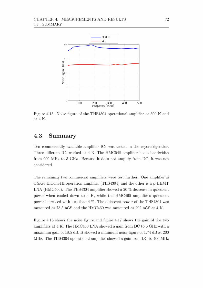
CHAPTER 4. MEASUREMENTS AND RESULTS 724.3. SUMMARY
100 200 300 400 5000
5
10
15
20
Frequency [MHz]
Noi
se F
igur
e [d
B]
300 K4 K
Figure 4.15: Noise figure of the THS4304 operational amplifier at 300 K andat 4 K.
4.3 Summary
Ten commercially available amplifier ICs was tested in the cryorefrigerator.
Three different ICs worked at 4 K. The HMC548 amplifier has a bandwidth
from 900 MHz to 3 GHz. Because it does not amplify from DC, it was not
considered.
The remaining two commercial amplifiers were test further. One amplifier is
a SiGe BiCom-III operation amplifier (THS4304) and the other is a p-HEMT
LNA (HMC460). The THS4304 amplifier showed a 20 % decrease in quiescent
power when cooled down to 4 K, while the HMC460 amplifier’s quiescent
power increased with less than 4 %. The quiescent power of the THS4304 was
measured as 73.5 mW and the HMC460 was measured as 292 mW at 4 K.
Figure 4.16 shows the noise figure and figure 4.17 shows the gain of the two
amplifiers at 4 K. The HMC460 LNA showed a gain from DC to 6 GHz with a
maximum gain of 18.5 dB. It showed a minimum noise figure of 1.74 dB at 200
MHz. The THS4304 operational amplifier showed a gain from DC to 400 MHz
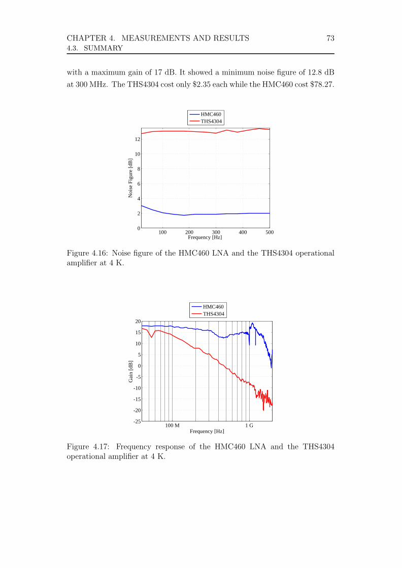
CHAPTER 4. MEASUREMENTS AND RESULTS 734.3. SUMMARY
with a maximum gain of 17 dB. It showed a minimum noise figure of 12.8 dB
at 300 MHz. The THS4304 cost only $2.35 each while the HMC460 cost $78.27.
100 200 300 400 5000
2
4
6
8
10
12
Frequency [Hz]
Noi
se F
igur
e [d
B]
HMC460THS4304
Figure 4.16: Noise figure of the HMC460 LNA and the THS4304 operationalamplifier at 4 K.
100 M 1 G-25
-20
-15
-10
-5
0
5
10
15
20
Frequency [Hz]
Gai
n [d
B]
HMC460THS4304
Figure 4.17: Frequency response of the HMC460 LNA and the THS4304operational amplifier at 4 K.
Chapter 5
Conclusions and Future Work
5.1 Research Findings
The project can be divided into two main section. The first section is the
SCE. The SCE was only simulated in WRSPICE and a final circuit was not
developed because of cost and time restrains. The second section was the
testing of commercially available amplifier ICs at 4 K. The s-parameters, noise
figure and quiescent power of the amplifiers was measured and compared to
its room temperature values.
5.1.1 Superconducting Electronics
Mainly two different amplifiers were considered in the SCE. The first was
a DC SQUID amplifier. It consists of a single input SQUID modulating a
100-SQUID series output array through a 50-turn modulation coil. The two
SQUID loops are connected in parallel, with the junction located between
them. A 100-SQUID series array with an input transformer with 36 primary
turns was shown by [13] to have a bandwidth of at least 175 MHz when
operated alone.
The second was a Suzuki stack amplifier. The Suzuki stack amplifier is a
superconducting digital logic amplifier for interfacing superconductor circuits
with semiconductor circuits. It provides a gigahertz amplifier to convert
low power superconducting RSFQ signals to higher power signal processing
74
CHAPTER 5. CONCLUSIONS AND FUTURE WORK 755.1. RESEARCH FINDINGS
circuits. It consists mainly of a lower IC Josephson Junction string in
parallel with a higher IC Josephson Junction string with an upper common
connection connected to the output terminal and a pulsed DC current source.
A ten-stage Suzuki stack amplifier was shown by [12] to have a bandwidth of
up to 10 GHz. The higher bandwidth of the Suzuki stack amplifier, made it
the preferred SCE amplifier.
The Suzuki stack amplifier was designed in WRSPICE and a circuit layout
was done in Lasi 6. The Hypres design rules were followed and a Monte
Carlo analysis was done with Hypres manufacturing tolerances included. A
DC-to-SFQ converter followed by a 250 µA JTL was used to generated the
RSFQ pulses.
The Suzuki stack amplifier consisted of four lower IC Josephson Junctions
with IC = 450µA and four higher IC Josephson Junctions with IC = 1mA.
The amplifier was synchronised by an external clock signal with a frequency
of 3.33 GHz that can be increased up to 7 GHz. The amplifier had a rise
time of 33 ps and a fall time of 31 ps. The peak voltage of the amplifier was
increased from 160 µA up to 8.2 mA and the peak current was increased from
160 µA to 430 µA.
The Monte Carlo analysis showed a success rate of 89.8 %. However, the
success of the circuit is mainly connected to the current received from the
external clock signal and can be adjusted until the correct output is received.
That will give the circuit a better success rate.
5.1.2 Commercially Available Amplifiers
Ten commercially available amplifier ICs were selected and tested in the
cryorefrigerator at 4 K. Each amplifier was soldered on its own specifically
designed PCB. A solid brass cover was used to connect the PCB to the cold
finger of the cryorefrigerator. RF cable and SMA connectors were used to
feed the input and output of the amplifier through the cryorefrigerator. The
cable had a maximum specified frequency of 3 GHz [27]. Three of the ten
CHAPTER 5. CONCLUSIONS AND FUTURE WORK 765.1. RESEARCH FINDINGS
amplifiers worked down to 4 K.
The first amplifier was the HMC548 LNA. It comprises of two internally
matched SiGe HBT amplifier stages. At room temperature, the HMC548 has
a gain between 720 MHz and 1.9 GHz with a maximum gain of 19.5 dB at 1.2
GHz. When the amplifier was cooled down the 4 K, it showed a gain from
820 MHz to 1.9 GHz with a maximum gain of 20 dB at 1.2 GHz.
The second amplifier was the HMC460 LNA. It comprises of a GaAs MMIC
p-HEMT LNA. The amplifier IC was firstly soldered on a FR4 PCB and
cooled down to 4 K. It showed a gain up to 1 GHz with a maximum gain
of 15.6 dB at room temperature and at 4 K. Then the evaluation board for
the HMC460 LNA was adjusted for cryogenic measurements. The amplifier
showed a gain over the complete 6 GHz spectrum of the spectrum analyser
with a maximum gain of 17 dB. When the amplifier was cooled down to 4 K,
the gain increased with up to 1.5 dB.
At room temperatures, the HMC460 LNA showed a minimum NF on the
evaluation board of 4 dB at 300 MHz. When the amplifier was cooled down
to 4 K, the NF dropped with more then 2 dB to reach a minimum NF of 1.74
dB with a gain of 17.4 dB at 200 MHZ. The amplifier had a quiescent power
of 292 mW at 4 K.
The third amplifier was the THS4304 SiGe BiCom-III operational amplifier.
It was designed to have a non-inverting gain of 17 dB. The amplifier showed
a gain up to 400 MHz at room temperatures, and a gain up to 475 MHz at 4
K. The NF of the amplifier dropped with more than 6 dB with a decrease in
temperature. At 4 K, it reached a minimum NF of 12.8 dB at 300 MHz with
a gain of 5.8 dB. The quiescent power of the amplifier decrease with 20 %,
from 92mW at 300 K to 73.5mW at 4 K.
Both the Bi-Com-III process from Texas Instruments Inc (THS4304) and the
p-HEMT process (HMC460) work down to 4 K. The HMC460 amplifier has
a wider frequency range, with a significantly lower NF than the THS4304.
CHAPTER 5. CONCLUSIONS AND FUTURE WORK 775.2. IMPROVEMENTS AND FUTURE WORK
However, the THS4304 has a lower quiescent power allowing it to reach 4 K
easier. The THS4304 cost only $2.35 each, while the HMC460 cost $78.27.
5.2 Improvements and Future Work
As mentioned through the thesis, the SCE was only simulated. The layout
of the SCE can be fabricated and physically tested in the cryorefrigerator.
Then the SCE can be matched to the selected amplifier IC. The complete
experiment can be set-up to detect and amplify RSFQ signals inside the
cryorefrigerator at 4 K. The signals can be amplified to have enough power to
be detected by room temperature electronics outside the cryorefrigerator.
Further tests can be done on different commercially available amplifier ICs,
to find a larger range of amplifiers that can work at 4 K. The cables and SMA
connectors inside the cryorefrigerator can be adjusted for higher frequencies
and better results.
Bibliography
[1] Hanamura, H., Aoki, M., Masuhara, T. and Minato, O.: Operation ofBulk CMOS Devices at Very Low Temperatures. IEEE Journal of solid-state circuits, , no. 3, pp. 484–490, 1983.
[2] Yoshikawa, N., Tomida, T., Tokuda, M. and Lui, Q.: Characterizationof 4K CMOS Devices and Circuits for Hybrid Josephson-CMOS System.IEEE Transactions on applied superconductivity, , no. 15, pp. 267–271,2005.
[3] HMC460LC5. Available at: http://www.hittite.com, [15 November2008], .
[4] Superconductors. Available at: http://superconductors.org/INdex.
htm, [24 October 2008].
[5] Buckel, W. and Kleiner, R.: Superconductivity: Fundamentals andApplications. 2nd edn. Wiley-VCH Publishing, 2004.
[6] Brock, D.K.: RSFQ Technology: Circuits and Systems. HYPRESS, Inc.,pp. 1–56, 2001.
[7] Fourie, C.J.: A Tool Kit for the Design of Superconducting ProgrammableGate Arrays. Ph.D. thesis, Electronic Engineering, University ofStellenbosch, Stellenbosch, South Africa, 2003.
[8] van Niekerk, P.C.: A Cryogenic CMOS-based Control Sysytem for TestingSuperconductor Electronics. Master’s thesis, Electronic Engineering,University of Stellenbosch, Stellenbosch, South Africa, 2007.
[9] PT405 Pulse Tube Cryorefrigerator. Available at: http://www.
cryomech.com/pt405-frontnback.pd, [06 October 2008.
[10] Ziemer, R.E. and Tranter, W.H.: Principles of Communication. Wiley,pp. 579–580, 2002.
78
BIBLIOGRAPHY 79
[11] Ebert, B., Humbla, S., Fell, A., Ortlepp, T. and Uhlmann, F.H.:Design of an ultra fast superconductor-to-semiconductor interface. 51.Internationales Wissenschaftliches Kolloquium, 2006.
[12] Przybysz, J.X. and Hills, P.: Superconducting digital logic amplifier.United States Patent, 1989.
[13] Clark, J., Goubau, W.M. and Ketchen, M.B.: Design of a hystereticSQUID as the readout for a DC SQUID. IEEE Transactions on appliedsuperconductivity, , no. 27, pp. 2910–2912, 1991.
[14] Welty, R.P. and Martinis, J.M.: Two-Stage integrated SQUID amplifierwith series array output. IEEE Transactions on applied superconductivity,pp. 2605–2608, 1993.
[15] Welty, R.P. and Martinis, J.M.: A series array of DC SQUID’s. IEEETransactions on applied magnetics, , no. 27, pp. 2924–2926, 1991.
[16] Meguro, S., Ikeda, S., Nagasawa, N. and Koike, A.: Hi-CMOS IIITechnology. Central research labratory, Hitachi, Ltd, 1984.
[17] High Electron Mobility Transistor. Available at: http://en.wikipedia.org/wiki/HEMT, [20 October 2008].
[18] Wuensch, S., Crocoll, E., Schubert, M. and Wende, G.: Design andDevelopment of a Cryogenic Semiconductor Amplifier for InterfacingRSFQ Circuits at 4.2 K. Superconductor science and technology, , no. 20,pp. 356–361, 2007.
[19] van Niekerk, P.C. and Fourie, C.J.: Cryogenic CMOS-based ControlSystem. IEEE Africon 2007, 2007.
[20] Whiteley, S.R.: Xic/WRSpice. Release 2.1.8. Circuit layout andsimulation software. Whiteley Research Incorporated, .
[21] Tolpygo, S.K. and Radparvar, M.: Niobium Integrated Circuit FabricationDesign Rules. Hypres, 2006. Process #03-10-45 Revision #23.
[22] Fourie, C.J. and Perold, W.J.: Simulated Inductance Variations in RSFQCircuit Structures. IEEE Transactions on Applied Superconductivity, ,no. 2, pp. 300–303, 2004.
[23] Bunyk, P.I. and Gilbert, K.C.: Automated calculation of MutualInductance Matrices of Multilayer Superconductor Integrated Circuits.Extended Abstracts ISEC, p. 62, 1993.
BIBLIOGRAPHY 80
[24] Kornev, V.K., Soloviev, I.I., Klenov, N.V. and Mukhanov, O.A.:Development of SQIF-Based Output Broad Band Amplifier. IEEETransactions on Applied Superconductivity, vol. 17, no. 2, pp. 269 – 272,June 2007.
[25] Perold, W.J., Jeffery, M., Wang, Z. and Duzer, T.V.: Superconductingcompementary output switching logic - a new superconducting voltage-state logic family. IEEE Transactions on Applied Superconductivity, vol. 6,no. 3, pp. 125 – 131, Sept 1996.
[26] Whiteley, S.R.: Sline Version 1.0. Whiteley Research Incorporated, .
[27] RG 316 Cable. Available at: http://www.hubersuhner.com, [15November 2008].
[28] Hollis, T.M., Comer, D.J. and Comer, D.T.: Optimisation of MOSAmplifier Performance Through Channel Length and Inversion LevelSelection, volume = 52, year = 2005. IEEE Transactions on circuitsand systems, , no. 9, pp. 545 – 549, Sept.
[29] High-Speed Processes. Available at: http://www.ti.com/research/
docs/highspeed.shtml, [25 June 2008].
[30] HMC548. Available at: http://www.hittite.com, [15 November 2008],.
[31] Technologies, A.: Fundamentals of RF and Microwave Noise FigureMeasurements. Application Note 57-1, 1998.