lecture 1 introduction to integrated circuit technologies
TRANSCRIPT

Lecture 1
Introduction to Integrated Circuit Technologies:
The importance of multidisciplinary understanding.
Reading:
Chapters 1 and parts of
2

Goal of this Course
The goal of this course is to teach
the fundamentals of Integrated
Circuit Technology
•Emphasis will be placed on
multidisciplinary
understanding using concepts
from Electrical Engineering,
materials science/engineering,
chemistry, physics, and
mechanical engineering.
Desired Outcome:
•Provide the student with
enough basic information so
he/she can understand
literature related to his/her
desired topic and allow
him/her to begin developing
new technologies.
Image after Plummer,
Deal, and Griffin
(2000)

Disciplines
ECE
•Electrical Design
•Electrostatic Field
Control
•Electrical behavior and
limits of materials and
material systems
•Using defects for our
electrical advantage
•Effects of strain and
stress on device
reliability
•Designing a better
device, circuit,
system
Material
Science
•Structural
Classification of
Materials:
Crystal Structure
•Formation and
control of defects,
impurity diffusion
•Strain and Stresses
materials
•Materials
interactions
(alloys, annealing)
•Phase
transformations
Chemistry
•Bonding
Classification of
Materials
•Etching and
deposition chemistry
•Chemical cleaning
Physics
•Quantum transport
•Solid state
descriptions of
carrier motion
Mechanical Engineering
•Heat transfer
•Micro-machines-Micro
Electro- Mechanical Machines
(MEMS)
•Fatigue/fracture, (especially for
packaging) etc...
•Mechanical stresses during processing
(polishing, thermal cycles, etc…)

ECE 6450 - Dr. Alan DoolittleGeorgia Tech
Disciplines
ECE
•Electrical Design
•Electrostatic Field
Control
•
l
Electrical behavior and
imits of materials and
aterial systems
Using defects for our
lectrical advantage
Effects of strain and
•
e
•
stress on
device
reliability
•Designing a better
device, circuit,
system
Material
Science
•Structural •Solid state
ssification of Materialsdescriptions of
rials: Crystal
Cla
Mate
Structure
•Formation and
control of defects,
impurity diffusion
•Strain and Stresses
materials
•Materials
interactions
(alloys, annealing)
•Phase
transformations
Chemistry
•Bonding
Classification of
•Etching and carrier motion
deposition chemistry
•Chemical cleaning
Physics
•Quantum transport
Mechanical Engineering
•Heat
•Mic
r
Mech
•Fat
i
pack
•Mec
transfer
o-machines-Micro Elect
anical Machines (MEM
gue/fracture, (especially
aging) etc...
hanical stresses during p
ro-
S)
for
rocessing
(polishing, thermal cycles, etc…)
Interested in the fundamental process
Interested
in the uses
of these
processes
Interestedm in the
uses of
these
processes

It is instructive to compare a EE’s outlook to Microelectronic Fabrication to that of
materials scientist.
Process Electrical Engineer/Scientist Materials
Scientist/Engineer
Epitaxial
Growth
forming the basic building blocks of a device Phase equilibria and
crystallography
Diffusion forming a E-Field gradient Solid solutions (just like sugar
in water)
Contact anneals may be looking to lower rectifying barrier,
improve adhesion or lower contact resistance
Alloying Process dictated by
material’s phase diagram
Si/SiO2 interface ability to form an insulator, maximizing
transistor/capacitor speed, controlling
threshold voltages or reduce recombination
of electron-hole pairs at the semiconductor
surface
Minimize interface defects
between two dissimilar crystal
structures

“Moore’s Law -- number of transistors/chip doubles every 2 years
due in large part to advanced materials processing methods!!
40048008
80808085 8086
286386
486Pentium® proc
P6
0.001
0.01
0.1
1
10
100
1000
1970 1980 1990 2000 2010Year
Tra
nsi
sto
rs (
MT
)2X growth in 1.96 years!

End of The Road: ITRS had previously predicted that the physical gate length of transistors would shrink until at least 2028 [see blue line]. The last ITRS report shows this feature size going flat in the coming years. But ITRS chair Paolo Gargini says that some further scaling may be possible after transistors go vertical.[Ref: http://spectrum.ieee.org/semiconductors/devices/transistors-could-stop-shrinking-in-2021]

Modern electronics consist of extremely small devices
Transistors in the above image are only a few microns (µm or 1e-6 meters) on a side.
Modern devices have lateral dimensions that are only fractions of a micron (~0.1 µm)
and vertical dimensions that may be only a few atoms tall.


The power of microelectronic
materials processing
Diameter: 13106 m (8103 miles)
Population: 6.7 billion people
Diameter: 0.2 m (8 inches)
Population: 10 billion components
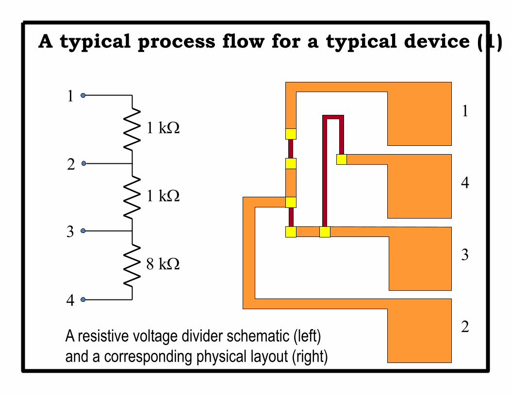
A typical process flow for a typical device (1)
1
2
3
4
1
2
3
4
8 kW
1 kW
1 kW
A resistive voltage divider schematic (left)
and a corresponding physical layout (right)

A typical process flow for a typical device (2)
pattern resistor material
deposit resistor material
grow oxide
starting wafer deposit insulator
pattern insulator
deposit metal
pattern metal

Intel Develops World's Smallest, Fastest CMOS Transistor
SANTA CLARA, Calif., Dec. 11, 2000 - Intel Corporation researchers have achieved a significant breakthrough by building the
world's smallest and fastest CMOS transistor. This breakthrough will allow Intel within the next five to 10 years to build microprocessors
containing more than 400 million transistors, running at 10 gigahertz (10 billion cycles per second) and operating at less than one volt.
The transistors feature structures just 30 nanometers in size and three atomic layers thick. (Note: A nanometer is one-
billionth of a meter). Smaller transistors are faster, and fast transistors are the key building block for fast microprocessors, the brains of
computers and countless other smart devices.
These new transistors, which act like switches controlling the flow of electrons inside a microchip, could complete 400
million calculations in the blink an eye or finish two million calculations in the time it takes a speeding bullet to travel one inch.
Scientists expect such powerful microprocessors to allow applications popular in science-fiction stories -- such as
instantaneous, real-time voice translation -- to become an everyday reality.
Researchers from Intel Labs are disclosing the details of this advance today in San Francisco at the International Electron
Devices Meeting, the premier technical conference for semiconductor engineers and scientists.
"This breakthrough will allow Intel to continue increasing the performance and reducing the cost of microprocessors well into
the future," said Dr. Sunlin Chou, vice president and general manager of Intel's Technology and Manufacturing Group. "As our researchers
venture into uncharted areas beyond the previously expected limits of silicon scaling, they find Moore's Law still intact."
Intel researchers were able to build these ultra-small transistors by aggressively reducing all of their dimensions. The gate oxides
used to build these transistors are just three atomic layers thick. More than 100,000 of these gates would need to be stacked to achieve the
thickness of a sheet of paper. Also significant is that these experimental transistors, while featuring capabilities that are generations beyond the
most advanced technologies used in manufacturing today, were built using the same physical structure as in today's computer chips.
"Many experts thought it would be impossible to build CMOS transistors this small because of electrical leakage problems,"
noted Dr. Gerald Marcyk, director of Intel's Components Research Lab, Technology and Manufacturing Group. "Our research proves that these
smaller transistors behave in the same way as today's devices and shows there are no fundamental barriers to producing these devices in high
volume in the future. The most important thing about these 30 nanometer transistors is that they are simultaneously small and fast, and work at
low voltage. Typically you can achieve two of the three, but delivering on all facets is a significant accomplishment."
“It's discoveries like these that make me excited about the future," added Chou. "It's one thing to achieve a great
technological breakthrough. It's another to have one that is practical and will change everyone's lives. With Intel's 30 nanometer transistor,
we have both."
For more information on Intel Silicon Technology Research, please reference Intel's new Silicon Showcase at
www.intel.com/research/silicon. Intel, the world's largest chip maker, is also a leading manufacturer of computer, networking and
communications products. Additional information about Intel is available at www.intel.com/pressroom. Source: Intel Web Page.
Famous Last Words: “I only want to design computers. I do not need to
know about ‘atoms and electrons’ ”. --- A Doomed Computer Engineer

Semiconductor substrates
(Campbell, Chap.2)
• Phase diagrams of semiconductor systems
• Crystallography and crystal structure
• Crystal defects
— 0-, 1-, 2-, and 3-D defects
— “defect engineering”
• Crystal growth processes
• Wafer preparation

The “semiconductor Periodic Table”
some metals
over here…
some gases
over here…
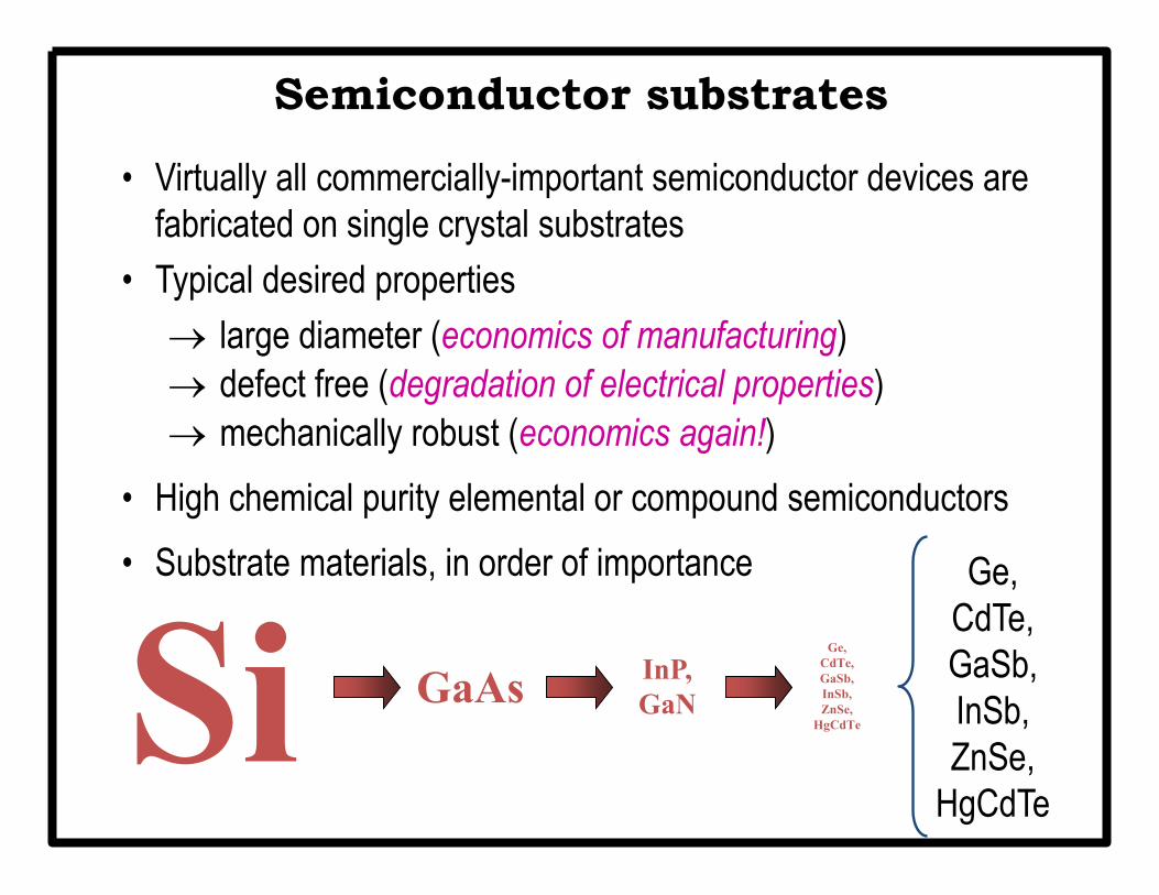
Semiconductor substrates
• Virtually all commercially-important semiconductor devices are
fabricated on single crystal substrates
• Typical desired properties
large diameter (economics of manufacturing)
defect free (degradation of electrical properties)
mechanically robust (economics again!)
• High chemical purity elemental or compound semiconductors
• Substrate materials, in order of importance
Si GaAsInP,
GaN
Ge,
CdTe,
GaSb,
InSb,
ZnSe,
HgCdTe
Ge,
CdTe,
GaSb,
InSb,
ZnSe,
HgCdTe

Properties of Silicon
• Density: 2.33 g cm-3
• Thermal expansion coefficient:
2.6 10-6 K-1
• Melting point: 1412°C
• Lattice parameter: 5.4308 Å
Properties of Germanium
• Density: 5.32 g cm-3
• Thermal expansion coefficient:
5.8 10-6 K-1 (large)
• Melting point: 937°C
• Lattice parameter: 5.6548 Å
~51022 atoms/cm3

Control of Conductivity is the Key to Modern Electronic Devices
•Conductivity, σ , is the ease with which a given material
conducts electricity.
•Ohms Law: V=IR or J=σE where J is current density
and E is electric field.
•Metals: High conductivity
•Insulators: Low Conductivity
•Semiconductors: Conductivity can be varied by
several orders of magnitude.
•It is the ability to control conductivity that make
semiconductors useful as “current/voltage control
elements”. “Current/Voltage control” is the key to
switches (digital logic including microprocessors etc…),
amplifiers, LEDs, LASERs, photodetectors, etc...

Classifications of Electronic Materials
Electrical/Computer engineers like to classify materials based on
electrical behavior (insulating, semi-insulating, and metals).
Chemists or Materials Engineers/Scientists classify materials
based on bond type (covalent, ionic, metallic, or van der Waals), or
structure (crystalline, polycrystalline, amorphous, etc...).
In 20-50 years, EE’s may not be using semiconductors at all!!
Polymers or bio-electronics may replace them! However the
materials science will be the same!

•For metals, the electrons can jump from the valence orbits (outermost core energy levels of the atom) to any
position within the crystal (free to move throughout the crystal) with no “extra energy needed to be supplied”
•For insulators, it is VERY DIFFICULT for the electrons to jump from the valence orbits and requires a huge
amount of energy to “free the electron” from the atomic core.
•For semiconductors, the electrons can jump from the valence orbits but does require a small amount of energy to
Classifications of Electronic MaterialsMaterials Classified based on bond strength
“free the electron” from the atomic core.

•Semiconductor materials are a sub-class of materials distinguished by the existence of a range of disallowed
energies between the energies of the valence electrons (outermost core electrons) and the energies of electrons
free to move throughout the material.
•The energy difference (energy gap or bandgap) between the states in which the electron is bound to the atom and
when it is free to conduct throughout the crystal is related to the bonding strength of the material, it’s density, the
degree of ionicity of the bond, and the chemistry related to the valence of bonding.
•High bond strength materials (diamond, SiC, AlN, GaN etc...) tend to have large energy bandgaps.
Classifications of Electronic MaterialsMaterials Classified based on bond strength
•Lower bond strength materials (Si, Ge, etc...) tend to have smaller energy bandgaps.
Classifications of Electronic Materials
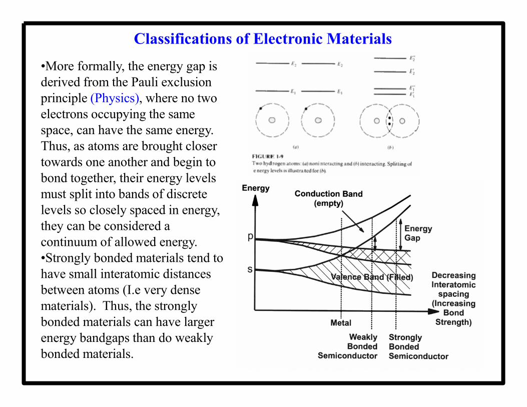
•More formally, the energy gap is
derived from the Pauli exclusion
principle (Physics), where no two
electrons occupying the same
space, can have the same energy.
Thus, as atoms are brought closer
towards one another and begin to
bond together, their energy levels
must split into bands of discrete
levels so closely spaced in energy,
they can be considered a
continuum of allowed energy.
•Strongly bonded materials tend to
have small interatomic distances
between atoms (I.e very dense
materials). Thus, the strongly
bonded materials can have larger
energy bandgaps than do weakly
bonded materials.

Consider the case of the group 4 elements, all** covalently bonded
Element Atomic Radius/Lattice Constant
(How closely spaced are the atoms?)
Bandgap
C
Si
Ge
α-Sn
Pb
0.91/3.56 Angstroms
1.46/5.43 Angstroms
1.52/5.65 Angstroms
1.72/6.49 Angstroms
1.81/** Angstroms
5.47 eV
1.12 eV
0.66 eV
~0.08 eV*
Metal
*Only has a measurable
bandgap near 0K
**Different bonding/Crystal
Structure due to unfilled
higher orbital states
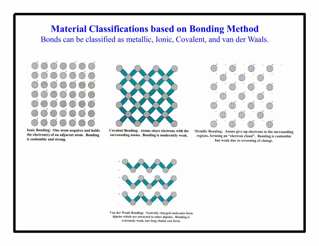
Material Classifications based on Bonding MethodBonds can be classified as metallic, Ionic, Covalent, and van der Waals.

Material Classifications based on Bonding MethodBonds can be classified as metallic, Ionic, Covalent, and van der Waals.

Classifications of Electronic MaterialsTypes of Semiconductors:
•Elemental: Silicon or Germanium (Si or Ge)
•Compound: Gallium Arsenide (GaAs), Indium Phosphide (InP), Silicon Carbide
(SiC), CdS and many others
•Note that the sum of the valence adds to 8, a complete outer shell. I.E. 4+4,
3+5, 2+6, etc...

Compound Semiconductors: Offer high performance (optical characteristics,
higher frequency, higher power) than elemental semiconductors and greater
device design flexibility due to mixing of materials.
Binary: GaAs, SiC, etc...
Ternary: AlxGa1-xAs, InxGa1-xN where 0<=x<=1
Quaternary: InxGa1-xAsyP1-y where 0<=x<=1 and 0<=y<=1
Half the total number of atoms must come from group III (Column III) and the
other half the atoms must come from group V (Column V) (or more precisely,
IV/IV , III/V, or II/VI combinations) leading to the above “reduced
semiconductor notation.
Example: Assume a compound semiconductor has 25% “atomic”
concentrations of Ga, 25% “atomic” In and 50% “atomic” of N. The chemical
formula would be:
Ga0.25In0.25N0.5
But the correct reduced semiconductor formula would be:
Ga0.5In0.5N
Classifications of Electronic Materials

Material Classifications based on Crystal Structure
Amorphous Materials
No discernible long range atomic order (no detectable crystal structure). Examples are silicon
dioxide (SiO2), amorphous-Si, silicon nitride (Si3N4), and others. Though usually thought of as less perfect than
crystalline materials, this class of materials is extremely useful.
Polycrystalline Materials
Material consisting of several “domains” of crystalline material. Each domain can be oriented
differently than other domains. However, within a single domain, the material is crystalline. The size of the
domains may range from cubic nanometers to several cubic centimeters. Many semiconductors are
polycrystalline as are most metals.
Crystalline Materials
Crystalline materials are characterized by an atomic symmetry that repeats spatially. The shape of
the unit cell depends on the bonding of the material. The most common unit cell structures are diamond,
zincblende (a derivative of the diamond structure), hexagonal, and rock salt (simple cubic).
Classifications of Electronic Materials

Classifications of Crystalline Electronic Materials
Hexagonal ( example: Wurzite)

The diamond crystal structure
• The diamond crystal structure is FCC with a two-atom basis
(000 and + FCC translations)
• Each atom is surrounded by four identical nearest neighbors in
a tetrahedral arrangement
• Examples: Si (51022 cm-3), Ge, a-Sn (group IV elements)
4
1
4
1
4
1

The zincblend crystal structure
• Like diamond, the zincblende structure is FCC with a two-atom
basis, but the atoms are different types
• Each A-atom is surrounded by four B-atom nearest neighbors in
a tetrahedral arrangement
• Commonly seen in stoichiometric compound semiconductors

The würtzite crystal structure
• The würtzite structure (right) is a
hexagonal variant of the
zincblende structure in which the
stacking order of the A-B
tetrahedra is varied
• Examples: GaN, CdS, AgI

Directions and Coordinates
• Positions within a unit cell are denoted in terms of fractional
coordinates x, y and z with respect to the unit cell basis vectors
a, b and c (note: right-handed coordinate system!!)
• The direction of any line is described by drawing a line through
the origin parallel to the given line and then assigning the
coordinates of any point on the line
Point A: coordinates 0 0 0
Point B: coordinates 1 1/2 0
Line AB: direction [1½0],
or clear fractions: [210]
Point C: coordinates 1 0 0
(or 0 0 0 in the next unit cell)
Point D: coordinates 1/3 1 1
(or – 2/3 1 1 w/ origin at C)
Line CD: direction [– 2/3 1 1]
or clear fractions: [233]

Crystallographic planes
• Planes in a crystal are denoted in terms of the Miller indices
which are the reciprocals of the fractional intercepts that the
planes make with the crystallographic axes
• If a plane is parallel to an axis, the intercept is taken to be at
infinity (); the reciprocal of infinity is 1/ = 0
a b c
The intercepts 3 2 2
The reciprocals 1/31/2
1/2
The Miller indices (1/31/2
1/2)
multiply by 6 (2 3 3)

Common crystallographic planes
in cubic systems
• Directions:
specific directions in brackets: [uvw]
negative directions [121] “one bar-two one”
equivalent directions: [111], [111] and [111] written <111>
• Planes:
specific planes in parentheses: (hkl)
negative indices (321) “bar-three two bar-one”
equivalent planes: (110), (011) and (101) written {110}

Crystal Growth: How do we get “Single Crystalline Material”?
The vast majority of crystalline silicon produced is grown by the Czochralski growth method. In this method, a
single crystal seed wafer is brought into contact with a liquid Silicon charge held in a crucible (typically SiO2 but
may have a lining of silicon-nitride or other material). The seed is pulled out of the melt, allowing Si to solidify.
The solidified material bonds to the seed crystal in the same atomic pattern as the seed crystal.

Ingot Growth
• First step in production of an
integrated circuit is growth of a
large piece of almost perfectly
crystalline semiconducting
material called an ingot (boule)
• Small seed crystal is suspended
in molten material then pulled
(1m/hr) and rotated (1/2 rps) to
form the ingot
• Result is an ingot approx. 1m
long and anywhere from 75 to
300 mm in diameter
• Dopant is almost always added
to the molten material
Page 39

Ingot Growth
ELEC 3908, Physical Electronics:
Basic IC Processing (4)David J. Walkey Page 40

Wafer Sawing
• Ingots are then sawed into wafers approximately 500-1000
μm (0.5 to 1 mm) thick using a diamond tipped saw
• Wafers are the starting material for integrated circuit
manufacture, and are normally referred to as the substrate
• Surface of the wafer is smoothed with combination of
chemical and mechanical polishing steps
ELEC 3908, Physical Electronics:
Basic IC Processing (4)David J. Walkey Page 41

Crystal Growth: Adding Impurities
Impurities can be added to the melt to dope the semiconductor as p-type or n-type. Generally, impurities “prefer
to stay in the liquid” as opposed to being incorporated into the solid. This process is known as segregation. The
degree of segregation is characterized by the segregation coefficient, k, for the impurity,
k =[Impurity in the Solid]
[Impurity in the Liquid]
Impurities like Al, kAl=0.002 prefers the liquid whereas B, kB=0.8 have very little preference.
Refer to Table 2.1 in your book for more k’s

Crystal Growth: Float Zone Refining
Since impurities can be introduced from the melt contacting the crucible, a method of purification without
contacting a crucible has been developed based on liquid-solid segregation of impurities. These crystals are
more expensive and have very low oxygen and carbon and thus, are not suitable for the majority of silicon IC
technology. However, for devices where a denuded zone can not be used these wafers are preferred.
Impurities are “kept out” of the single crystal by the liquid-solid segregation process.
Good for
Solar cells,
power
electronic
devices that
use the entire
volume of the
wafer not just
a thin surface
layer, etc…

Crystal Growth: GaAs
GaAs Liquid Encapsulated CZ (LEC)
GaAs is more difficult. At 1238 C, the vapor pressure of As is ~10 atmospheres while Ga is only
~0.001 atmospheres. Thus, at these temperatures, As is rapidly lost to evaporation resulting in a
non-stoichiometric melt. (Recall from the phase diagram that 50% Ga and 50% As is required to
get pure GaAs). Thus, a cap is used to encapsulate the melt. This cap is typically Boric oxide
(B2O3) and melts at ~400 C, allowing the seed crystal to be lowered through the cap and pulled
out of the cap.

Crystal Growth: GaAs
Horizontal Bridgman GaAs Growth
Historically, limitations on defect densities possible with LEC limit the use of LEC wafers to electronic
applications. Most GaAs for optoelectronics (requiring low defect densities) is produced by the bridgman
method. In this method and it’s many variants, the GaAs charge is held in a sealed ampoule with excess
arsenic. Thus, higher pressures can be reached that limit As evaporation. The charge is heated, partially
melted with the melt then brought into contact with a seed crystal. The molten region is then moved through
the charge allowing the trailing edge of the molten region to solidify into a low defect single crystal while the
leading edge of the molten region melts more of the charge.

P P
N+N+N+
P
Enhancement Mode: Normally Off (have to do something to get it to conduct electricity)
Depletion Mode: Normally On (have to do something to get it to stop conducting electricity)
P NN+
Depletion TransistorEnhancement Transistor
The Need for Multidisciplinary Understanding:Consider the simple inverter in NMOS technology using Depletion Load Transistors
Source Source
Drain Drain
GateGate

polymers
Photoresist
Si3N4
SiO2
Disciplines Used: ECE (choice of p-type layers and doping concentrations),
Chemistry (CVD), MSE (solid solutions of dopants), Physics (small devices)
Materials Used: Crystalline Semiconductors, amorphous dielectrics,
Following initial cleaning, a thin epitaxial region is grown via chemical vapor deposition
followed by a SiO2 layer thermally grown on the silicon substrate. A Si3N4 layer is then
deposited by LPCVD. Photoresist is spun on the wafer to prepare for the first masking
operation.
P-
P+

amorphous dielectrics, polymers
Disciplines Used:
physics)
Chemistry (etching), Physics (optics/diffraction, plasma
Materials Used: Acids, bases, dry plasmas, Crystalline Semiconductors,
SiO2
Photoresist
Si3N4-x
Mask #1 patterns the photoresist. The Si3N4 layer is removed where it is not protected by the
photoresist by dry etching.
P

P
Disciplines Used: ECE (electrical design of edge termination layers),
Chemistry (choice of dopants), MSE (solid solutions of dopants), Physics (Ion
bombardment)
Materials Used: Crystalline Semiconductors, amorphous dielectrics,
polymers
P Implant
A boron implant prior to LOCOS oxidation increases the substrate doping locally under
the field oxide to minimize field inversion problems.
Boron Boron
Photoresist
Si3N4-x
SiO2

P
Disciplines Used: ECE (electrical design of isolation), Chemistry (oxidation
reactions and barriers), MSE (solid solutions of dopants)
Materials Used: Amorphous dielectrics, toxic/corrosive gases
P P
During the LOCOS oxidation, the boron implanted regions diffuse ahead of the growing
oxide producing the P doped regions under the field oxide. The Si3N4 is stripped after the
LOCOS process.
Si3N4-x
SiO2

P
P P
As or Phos
Photoresist
Disciplines Used: ECE (electrical design of channel), Chemistry (choice of
dopants), MSE (solid solutions of dopants), Physics (Ion bombardment)
Materials Used: Crystalline Semiconductors, amorphous dielectrics,
polymers, and ions
N
Mask #2 is used for the the threshold shifting implant for the depletion transistors. An N type
dopant is implanted.
SiO2

P
P P
P N
B
Photoresist
Disciplines Used: ECE (electrical design of channel), Chemistry (choice of
dopants), MSE (solid solutions of dopants), Physics (Ion bombardment)
Materials Used: Crystalline Semiconductors, amorphous dielectrics,
polymers, and ions
Mask #3 is used to mask the threshold shifting implant for the enhancement transistors. A P
type dopant is implanted.
SiO2

P
Disciplines Used: ECE (electrical design of isolation, electrical reliability),
Chemistry (oxidation reactions), MSE (solid solutions of dopants)
Materials Used: Amorphous dielectrics, gases
P P
P N
After etching back the thin oxide to bare silicon, the gate oxide is grown for the MOS
transistors.
SiO2

P
Disciplines Used: ECE (electrical design of source), Chemistry (choice of
dopants), MSE (solid solutions of dopants), Physics (optics/diffraction)
Materials Used: Crystalline Semiconductors, amorphous dielectrics,
polymers, and ions
P P
P N
Mask #4 is used to provide the buried contact. The gate oxide is etched where the poly
needs to contact the silicon.
Photoresist
SiO2

P
P P
P N
A layer of polysilicon is deposited. Ion implantation of an N type dopant follows the
deposition to heavily dope the poly.
amorphous dielectrics, gases
Disciplines Used: ECE (electrical design of source, reliability), Chemistry(CVD & choice of dopant for poly), MSE (alloy reactions)
Materials Used: Crystalline and poly-crystalline Semiconductors,
Poly-XSiO2
P
P P
P N
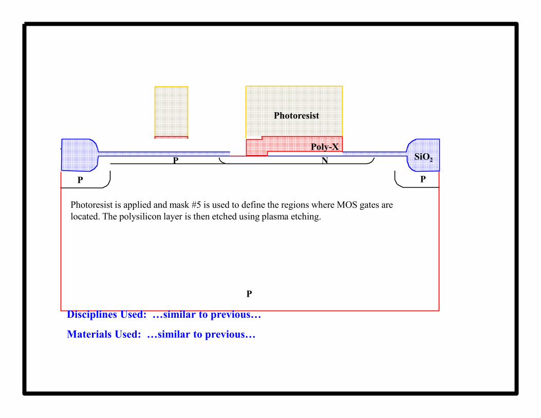
Photoresist is applied and mask #5 is used to define the regions where MOS gates are
located. The polysilicon layer is then etched using plasma etching.
Disciplines Used: …similar to previous…
Materials Used: …similar to previous…
Photoresist
Poly-XSiO2

P
P PN+ Implant
P N
Arsenic
Poly-X
Disciplines Used: …similar to previous…
Materials Used: …similar to previous…
Arsenic is implanted to form the source and drain regions. Note that this can be unmasked
because there are only NMOS transistors on the chip.
SiO2

P
P P
N+N+N+ P
Disciplines Used: …similar to previous…
Materials Used: …similar to previous…
NN+
A final high temperature drive-in activates all the implanted dopants and diffuses junctions
to their final depth. The N doping in the poly outdiffuses to provide the buried contact.
SiO2
Poly-X
P
P P
N+N+N+ P
Disciplines Used: …similar to previous…
Materials Used: …similar to previous…
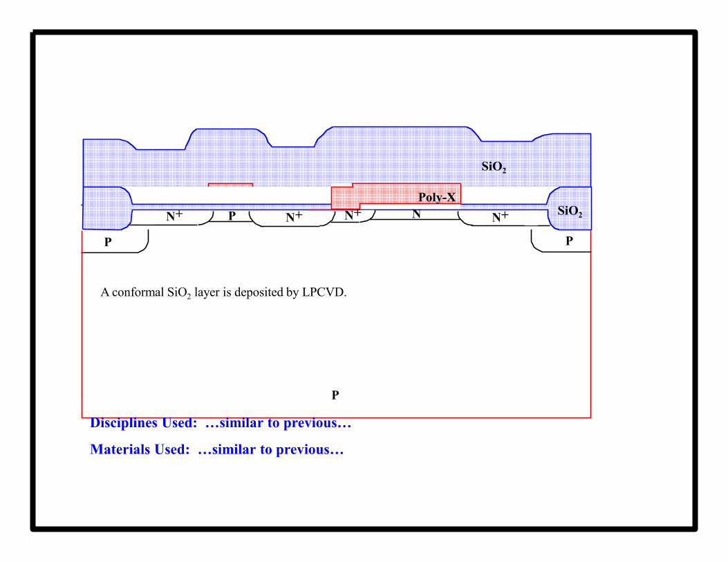
NN+
A conformal SiO2 layer is deposited by LPCVD.
SiO2
SiO2
Poly-X

P
P P
N+N+N+ P
Disciplines Used: …similar to previous…
Materials Used: …similar to previous…
NN+
Mask #6 is used to define the contact holes.
SiO2
Photoresist
Poly-X

P
P P
N+N+N+ P
Disciplines Used: …similar to previous…
Materials Used: …similar to previous…
NN+
Aluminum is deposited on the wafer.
SiO2
Al, Cu/Al
Poly-X

P P
N+N+N+
Mask #7 is used to pattern the aluminum. After stripping the resist, the structure is finished to
the point shown in the cross-section we started with. In actual practice an additional deposition
of a final passivation layer and an additional mask (#8) would be needed to open up the
regions over the bonding pads.
P
Disciplines Used: …similar to previous…
Materials Used: …similar to previous…
P NN+
SiO2
Photoresist
Al, Cu/Al
Poly-X

P P
N+N+N+
P
Disciplines Used: …similar to previous…
Materials Used: …similar to previous…
P NN+
Depletion TransistorEnhancement Transistor
Final environmental barrier deposited for encapsulating the device. Openings would be
provided only at bond pads.
SiO2
Polymer or SiNx
Encapsulation
Al, Cu/Al
Poly-X

Classifications of the many processes used in
Integrated Circuit Technology
Unit I: Hot (or energetic) Processes
•Diffusion (chapter 3)
•Thermal Oxidation (chapter 4)
•Ion Implantation (chapter 5)
•Rapid Thermal Processing (chapter 6)
Unit II: Pattern Transfer
•Optical Lithography (chapter 7)
•Photoresists (chapter 8)
•Non-Optical Lithographic Techniques (chapter 9)
•Vacuum Science and Plasmas (chapter 10)
•Etching (chapter 11)
Unit III: Thin Films
•Physical Deposition: Evaporation and Sputtering (chapter 12)
•Chemical Vapor Deposition (chapter 13)
•Epitaxial Growth (chapter 14)
Unit IV: Process Integration
•Selected topics from Silicon (chapters 16 & 18), GaAs (chapter 17)
and yield Analysis (chapter 19)

Semiconductor Substrates

Phase Diagrams
•Only certain compositions of materials are allowed at a given temperature and pressure
when the material is in thermodynamic equilibrium. These compositions can be described
by “Phase Diagrams”. These allowed compositions effect semiconductor growth, and
dictate the stability and electrical properties of metal- semiconductor contacts.
• A phase diagram contains a “map” of a materials state including liquid only, solid only,
coexisting as liquid with solid, or even various crystal structures of solid phases verses
changes in material temperature, composition or pressure. We will only examine phase
diagrams at a single pressure.

Solid
Liquid
Consider the SiGe material system.
Things to know about phase diagrams:
1.) Note the melting points of pure Ge and pure Si.
2.) Identify the Solid, Liquid and combination regions as well as
the solidus (S/L+S) and liquidus (L/L+S) lines.
3.) Assume a 40% atomic Si composition of the starting material
(thoroughly mixed
powder).
4.) As the material is heated from room temperature it starts in a
“single phase field” (I.e, solid phase) and the composition
remains
the same, 40% atomic Si. However, as the temperature is elevated,
the material begins melting at ~1070 degrees entering into a
“two phase field” containing part liquid and part solid.
When the material reaches ~1230 degrees, the material is
completely melted and enters a “single phase field” (liquid) again.
When in the solid or liquid regions, the composition is
identical to the original composition (40%).
5.) When the 1070<Temperature<1230, both liquid and solid
phases coexist. However, the composition of the liquid and solid
materials can differ from the original composition. For example at
1200 C, draw a horizontal “tie line” (shown as green and
purple) from the liquidus line to the solidus line. Read off the
compositions of the liquid, 34%at Si, and the solid, 67% at Si.
Note that the compositions of the solid and liquid are different.
6.) The amount of the melt that is solid and the amount that is
liquid can be determined by the line, and
the liquidus line. “Tie line” between the
solidus line, and the liquidus line.% Liquid
67 40 x 100 81.8%
67 34
o x 100% LiquidX S X L
X XS
XSXL Xo
Determine
the Composition of
the Liquid and
solid
% Solid40 34
x 100 18.2%67 34
L x 100X S X L
X Xo% Solid

Consider the Si-Al material system.
Weight Percent Silicon99.97 99.98 99.99
99.97 99.98 99.99
Atomic Percent Silicon
Tem
per
atu
re(C
)
1400
1200
1000
800
600
99.96
99.96
1400
1200
1000
800
600577 (C)(Al)+(Si)
(Si)
L-(Si)
L
L-(Si)
L
L-(Al)
L-(Al)
Things to know about phase diagrams:
7.) In certain material systems a Horizontal, isothermal boundary exists that indicates the existence of phase transformations involving
three phases. If and are solid phases, we can classify the transformations as a:
a.) Eutectic: L-->
b.) Eutectiod: -->
c.) Peritectic: L +
Si-Al experiences a “Eutectic” transformation at 577 C. Note this is lower than the melting point of Al (660 C) and Si (1412 C). At this
temperature, a liquid containing 11.3% Si will transform to two solid phases, (Al with 1.59%Si) + (Si + minimal fraction of Al-I.e. Al doped)
Si containing Al
(Al Doped)
Al
containing
Si

Consider the Si-Al material system.
Si-Al “Eutectic” transformation at 577 C. Note this is lower than the melting point of Al (660 C) and Si (1412 C). At this temperature, a
liquid containing 11.3% Si will transform to two solid phases, (Al with 1.59%Si) + (Si + minimal fraction of Al-I.e. Al doped)
Chunks/Flakes
of Si in the Al-
Si mix.
Figures from and a great explanation of phase diagrams in
more detail than we have discussed here can be found at:
http://www.soton.ac.uk/~pasr1/index.htm

Crystalline defects can be classified
as: 1.) Point defects
2.) Line defects
3.) Planar defects
4.) Volume defects.
1.) Point Defects: Some include Vacancies (Schottky defect), interstitials, substitutional, and
impurity-vacancy complexes (Frenkel defect, SiI - V, is shown).
Point Defects dictate most diffusion mechanisms, and thus, determine the impurity profile.
Defects in Semiconductors

Normal
Bonding
Rearrangement
of Bonds at a
Vacancy
Point Defects: Vacancies
Charge neutrality must exist in the crystal. When a vacancy is created,
1.) it can cleanly brake all four bonds ==> Neutral vacancy, Vo, neutral Interstitial,
2.) n electrons may stay at the vacancy ==> V-n + I+n,
3.) n electrons may go with the interstitial==> V+n + I-n
The number of neutral vacancies is thermodynamically determined by,
where No is the density of Atoms/cm3 and Ea is the activation energy for the formation of the vacancy (in
silicon, No=5.02e22 cm-3 and Ea=2.6 eV)
Singularly and doubly charged vacancies have concentrations that depend on the number of carriers present,
V 0 Na
e kTE
O
V V 0 n f n,T
ni
V V 0 nf n 2 ,T
ni
2
V V 0 p f p,T
ni
V V 0 f p 2 ,Tni
p2

Point Defects: Interstitials
Atoms not residing on lattice sites are called interstitials. They can be foreign,
unwanted impurities, intentionally introduced impurities, or “misplaced” host
atoms. Dopant atoms diffuse through the semiconductor faster as interstitials, but
we need to place them in substitutional sites to make use of them.
Oxygen
Interstitial
Equivalent
Oxygen Sites

Point Defects: Substitutional
Impurities can replace a host atom in the lattice site. They can be foreign,
unwanted impurities, or intentionally introduced impurities. You may want
a dopant impurity to be on a substitutional site, but you may not want a
heavy metal atom or other unwanted impurity to be on a substitutional site
(harder to remove).
Si Lattice
Carbon

Line Defects: Dislocations
The term, “threading”, describes specific cases in
which the dislocation “threads” through a grown
layer
(i.e. starts at or near the substrate and ends on the
A missing line or additional line of atoms is called a dislocation.
Dislocations are either pure edge, pure screw or a combination of
both type called mixed character.
surface).

Planar Defects: Grain Boundaries & Stacking Faults
Two dimensional defects include:
1.) Grain boundaries in polycrystalline materials
2.) Stacking faults in crystalline material.
A grain boundary is an array of dislocations that line up to form a plane that forms a
boundary between two crystalline regions (grains) that are misoriented relative to one
another.
High Angle Grain
Boundaries
Low Angle Grain
Boundary

Planar Defects: Stacking Faults
A stacking fault is a disruption in the stacking of layers in the crystal.

Volume Defects: Precipitates
Precipitates are three dimensional defects that have a different chemical makeup from the host
lattice. They can result from an impurity exceeding the maximum solubility of the crystal (much
like supersaturation of sugar in water). Generally, these defects are harmful, but they do have
some technological value - oxygen gettering to form a denuded zone and As precipitates for high
speed optical devices.
•External Gettering: Roughing the backside of
the wafer to provide a low energy “sink” for
impurities.
•Internal gettering: Using internal defects to
trap impurities moves impurities away from the
active region of the wafer, were transistors are
to be formed. Oxygen precipitates are the
gettering sites. 15 to 20 ppm Oxygen wafers
are required. Less than 15 ppm - precipitate
density is too sparse to be an effective gettere
Greater than 20 ppm, wafers tend to warp
during the high temperature process. Note:
devices that use the entire wafer as the active
region (solar cells, thyristors, power diodes,
etc...) can not use this technique, but can use
extrinsic gettering. Today, most wafer
manufactures perform this task.
r.
Roughened Back side
Gettered Bulk and Surface

Volume Defects: Oxygen Precipitates
t e kT1.2e
VLd 0.091cm2
sec
Oxygen in Si 2x10²¹ atomse
1.032eV
kT cm3
A given denuded zone may need to have minimal Oxygen (to prevent precipitation in the active
regions of devices during later thermal cycles) and be of a required depth (enough “clean material to
form the active device region).
These are determined by:

Microelectronic unit processes
• Diffusion
• Thermal oxidation
• Ion implantation
• Rapid thermal processing
• Optical lithography
• Non-optical lithography
• Etching
• Physical vapor deposition
• Chemical vapor deposition
• Epitaxial growth
• Metallization
“hot” processes -- cause a
physical change in a material
transformation processing
pattern transfer -- requires the
removal of material
subtractive processing
thin film growth -- results in the
deposition of material
additive processing