lecture 10: cache coherence - carnegie mellon...
TRANSCRIPT
Parallel Computer Architecture and Programming CMU / 清华⼤大学, Summer 2017
Lecture 10:
Cache Coherence

CMU / 清华⼤大学, Summer 2017

CMU / 清华⼤大学, Summer 2017
Course schedule (where we are)
Week 1: How parallel hardware works: types of parallel execution in modern processors SPMD programming
Week 2: Techniques for writing parallel programs (efficient scheduling + enhancing locality) GPU programming
Week 3: How parallel hardware works: cache coherency and memory consistency Details of implementing and using synchronization (locks)
Week 4: How modern hardware works: heterogeneity and specialization A modern trend: domain specific programming systems
CMU / 清华⼤大学, Summer 2017
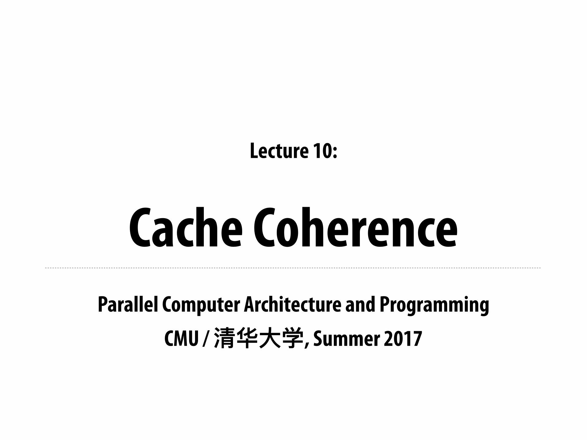
Cache review
Dirty Bit Tag Data (64 bytes)
Consider one int of data with value = 1, at 32-bit memory address: 0x12345604Below: cache with storage for 16 cache lines
0 1 2 3 4 5 6 7 8 9
10 11 12 13 14 15
Where does the data in the cache go? (assume the cache is “direct mapped”)
CMU / 清华⼤大学, Summer 2017
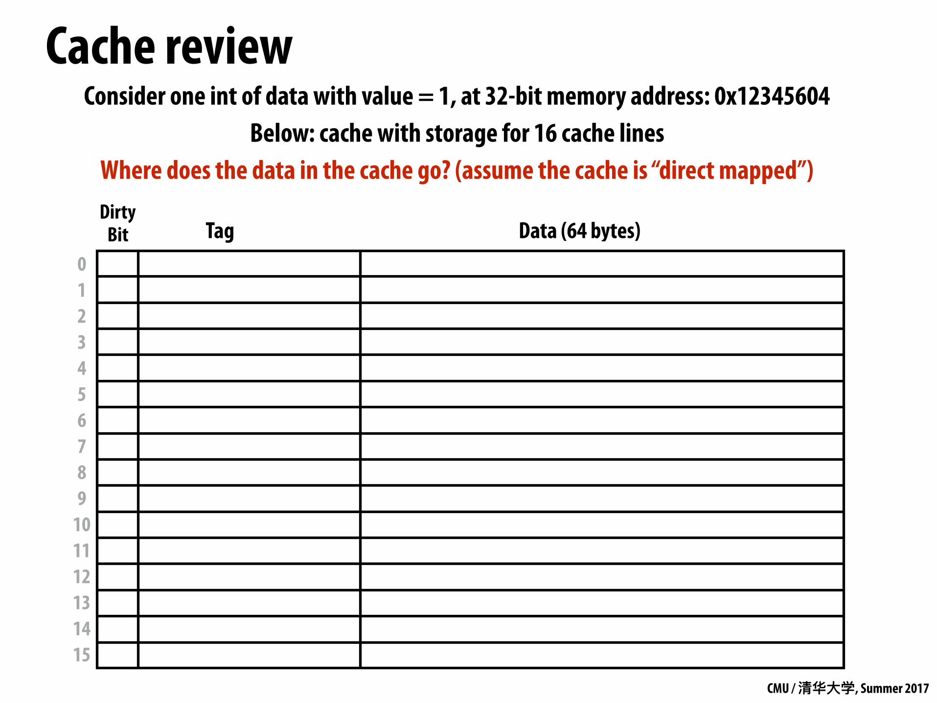
Cache review
Dirty Bit Tag Data (64 bytes)
00010010001101000101011000000100
0 1 2 3 4 5 6 7 8 9
10 11 12 13 14 15
Set (4 bits)Tag (22 bits) Starting byte (6 bits)
0001 0010 0011 0100 0101 01
Consider one int of data with value = 1, at 32-bit memory address: 0x12345604
1 0 0 0
byte 0 of cache line byte 63 of cache line
CMU / 清华⼤大学, Summer 2017
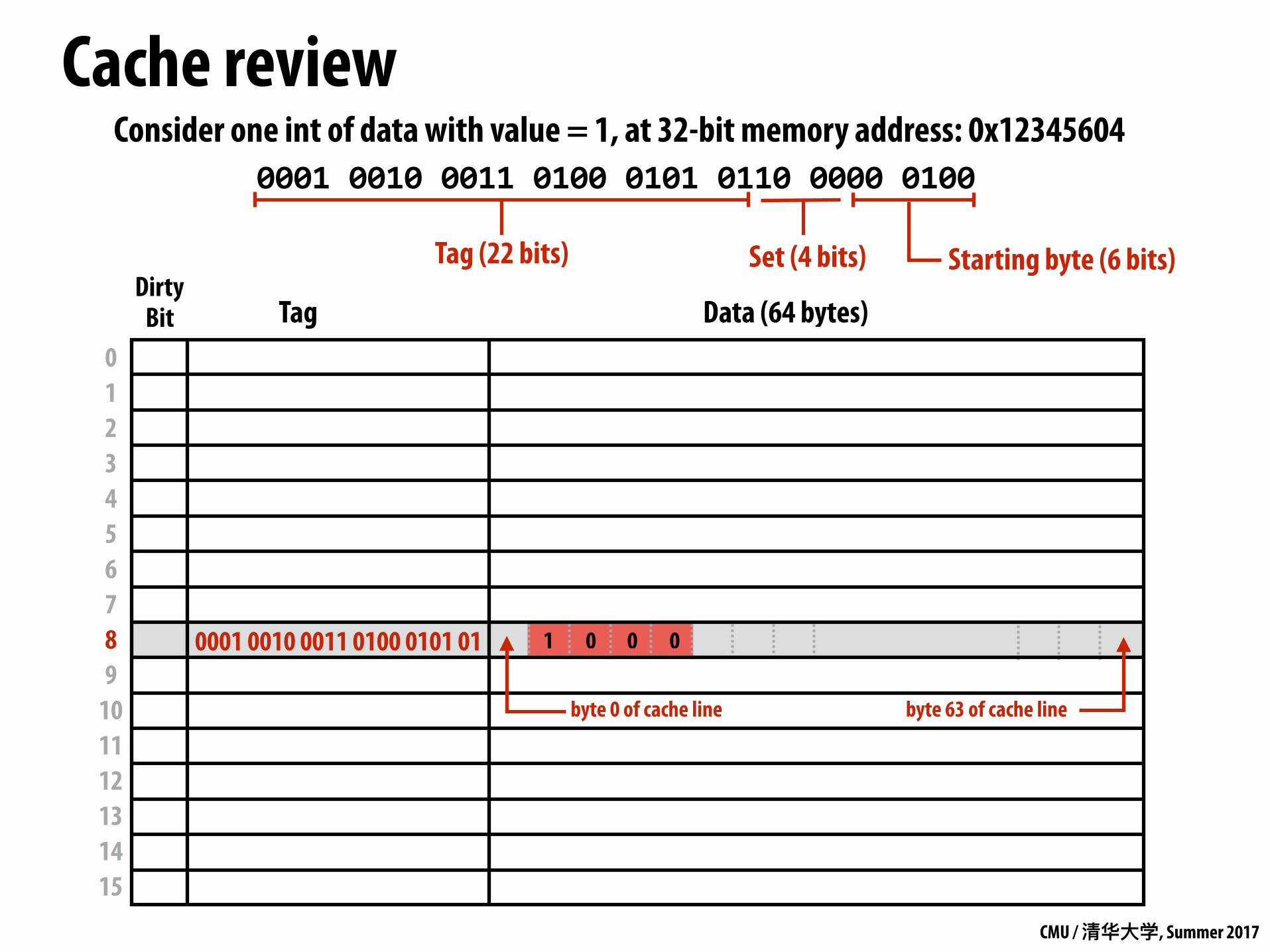
Set associative cache
Dirty Bit Tag Data (64 bytes)
0
1
2
3
4
5
6
7
0001 0010 0011 0100 0101 011 1 0 0 0
00010010001101000101011000000100
Set (3 bits)Tag (23 bits) Starting byte (6 bits)
Two cache lines per set (can place line at either location — must check two tags to find line)

CMU / 清华⼤大学, Summer 2017
Terminology▪ “Write back” cache
- Store instructions modify contents of data in cache, but modification do not immediately made to memory
- Cache tracks with lines have been modified (“dirty” lines)
- Write of modified cache line to memory is delayed until line is “evicted” from cache
- Alternative: write-through cache (cache writes data value modifications to memory after every store instructions)
▪ Why write-back caches? - If processor writes to same value many times, only write to memory once!
- Save memory bandwidth!
CMU / 清华⼤大学, Summer 2017
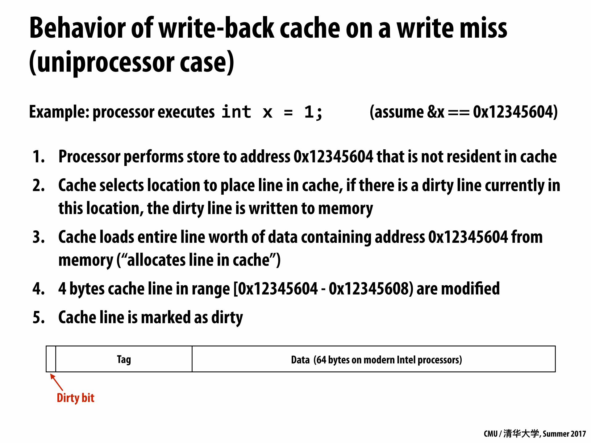
Behavior of write-back cache on a write miss (uniprocessor case)Example: processor executes intx=1; (assume &x == 0x12345604)
1. Processor performs store to address 0x12345604 that is not resident in cache
2. Cache selects location to place line in cache, if there is a dirty line currently in this location, the dirty line is written to memory
3. Cache loads entire line worth of data containing address 0x12345604 from memory (“allocates line in cache”)
4. 4 bytes cache line in range [0x12345604 - 0x12345608) are modified
5. Cache line is marked as dirty
Data (64 bytes on modern Intel processors)Tag
Dirty bit

CMU / 清华⼤大学, Summer 2017
A shared memory multi-core processor▪ Processors read and write to shared variables
- More precisely: processors issue load and store instructions
▪ A reasonable expectation of memory is: - Reading a value at address X should return the last value written to
address X by any processor
Processor Processor Processor Processor
Interconnect
Memory I/O
(A simple view of four processors and their shared address space)
CMU / 清华⼤大学, Summer 2017
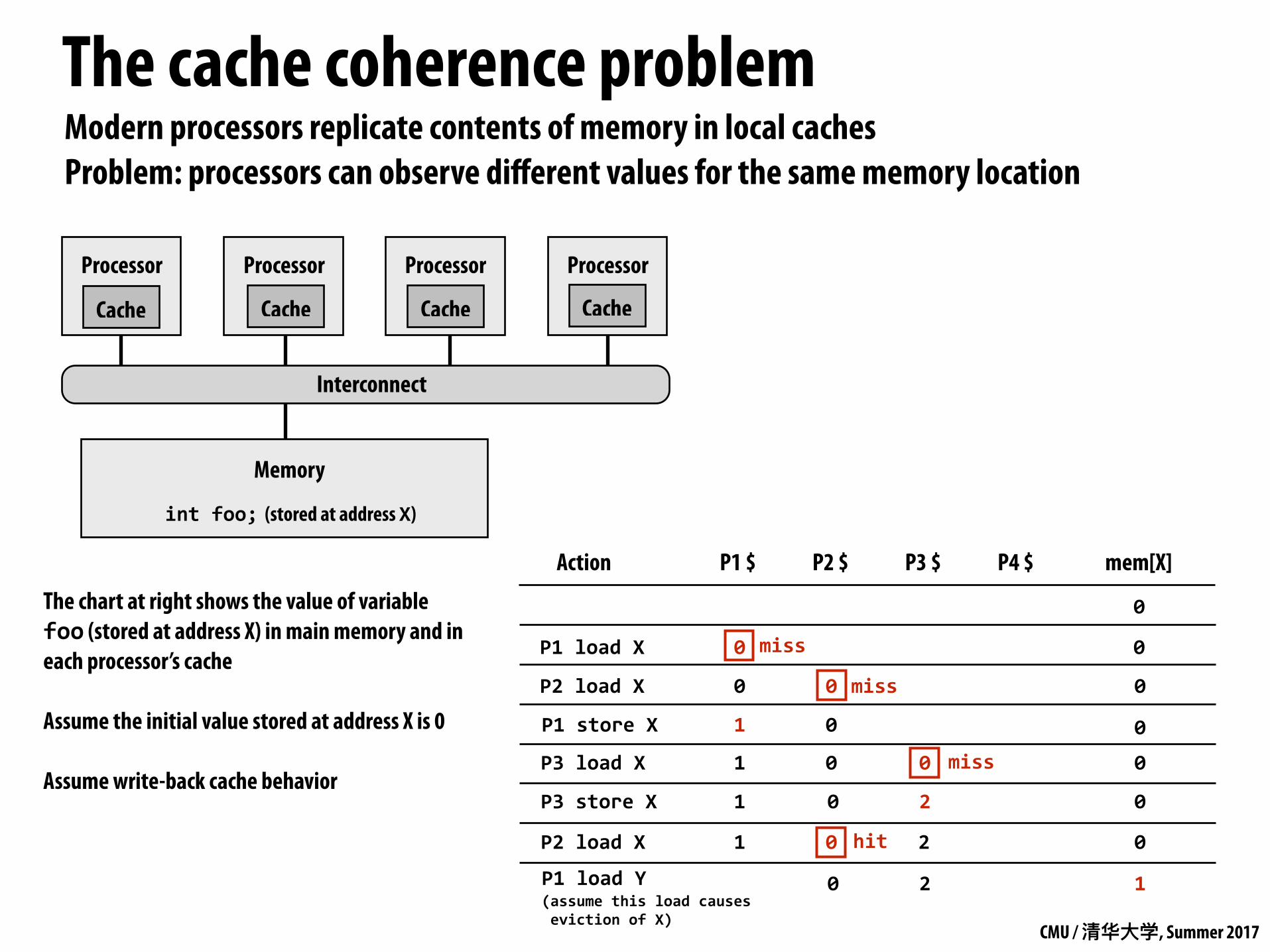
The cache coherence problemModern processors replicate contents of memory in local caches Problem: processors can observe different values for the same memory location
Processor Processor Processor Processor
Interconnect
Memory
Cache Cache Cache Cache
P1 $ P2 $ P3 $ P4 $ mem[X]Action
0
intfoo; (stored at address X)
P1storeX 1 0 0
P1loadY(assumethisloadcausesevictionofX)
10 2
The chart at right shows the value of variable foo (stored at address X) in main memory and in each processor’s cache
Assume the initial value stored at address X is 0
Assume write-back cache behaviorP3loadX 01 0 0 miss
01 0 2P3storeX
P2loadX 01 0 2hit
P2loadX 0 0 0miss
P1loadX 0 0miss

CMU / 清华⼤大学, Summer 2017
The cache coherence problemIs this a mutual exclusion problem? (Can you fix the problem by adding locks to your program?)
Processor Processor Processor Processor
Interconnect
Memory
Cache Cache Cache Cache
P1 $ P2 $ P3 $ P4 $ mem[X]Action
0
intfoo; (stored at address X)
P1storeX 1 0 0
P1loadY(assumethisloadcausesevictionofX)
10 2
0P3loadX 1 0 0 miss
P3storeX 01 0 2
P2loadX 01 0 2hit
P2loadX 0 0 0miss
P1loadX 0 0miss
The chart at right shows the value of variable foo (stored at address X) in main memory and in each processor’s cache
Assume the initial value stored at address X is 0
Assume write-back cache behavior
NO! This is a problem created by replicating the data stored at address X in local caches (a hardware implementation detail)
CMU / 清华⼤大学, Summer 2017
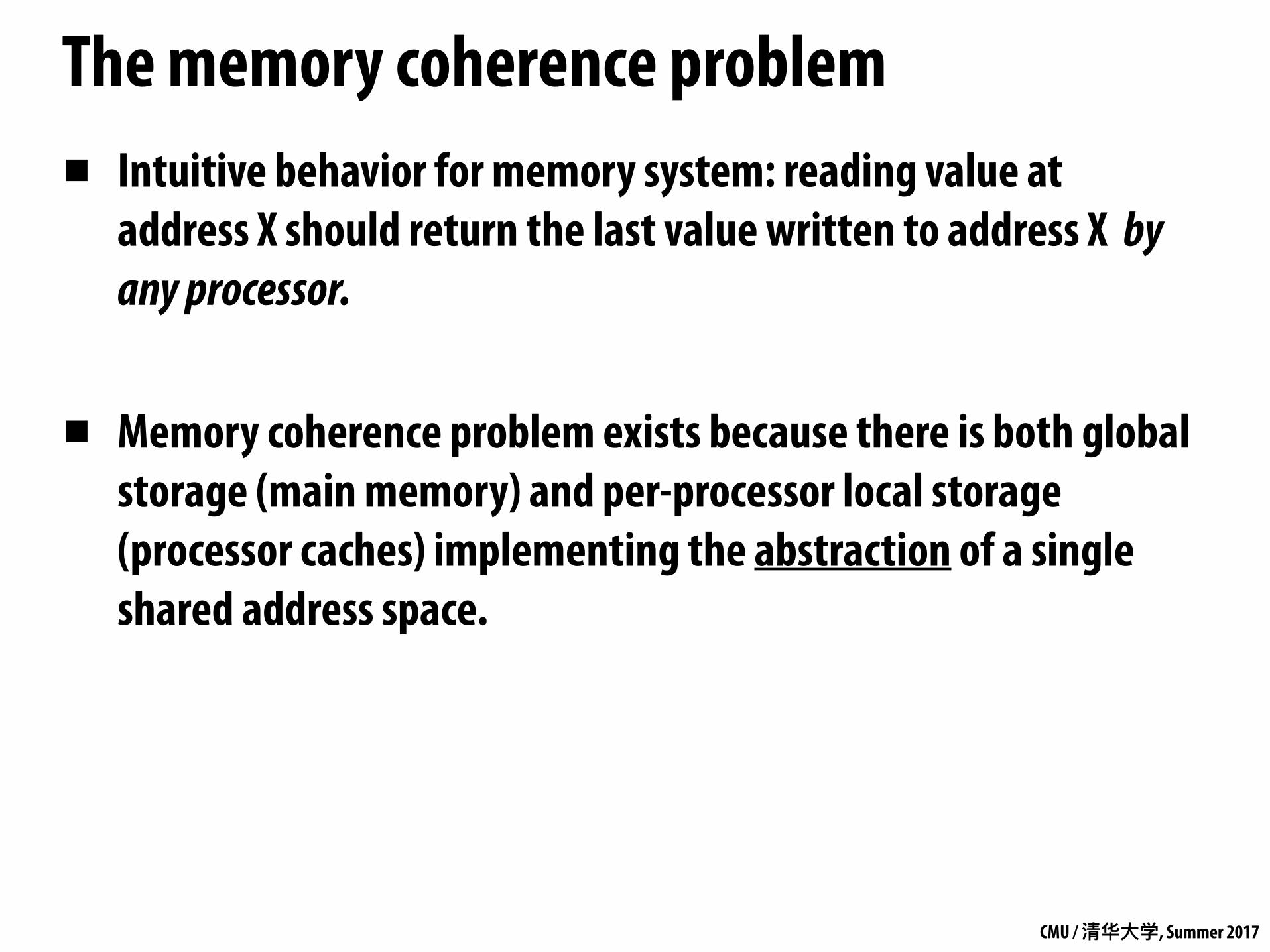
The memory coherence problem▪ Intuitive behavior for memory system: reading value at
address X should return the last value written to address X by any processor.
▪ Memory coherence problem exists because there is both global storage (main memory) and per-processor local storage (processor caches) implementing the abstraction of a single shared address space.

CMU / 清华⼤大学, Summer 2017
Cache hierarchy of Intel Skylake CPU (2015)
Core
L1 Data Cache
L2 Cache
Shared L3 Cache (One bank per core)
Ring Interconnect
Core
L1 Data Cache
L2 Cache
Core
L1 Data Cache
L2 Cache
Core
L1 Data Cache
L2 Cache
L1: (private per core) 32 KB 8-way set associative, write back 2 x 32B load + 1 x 32B store per clock 4 cycle latency
L2: (private per core) 256 KB 4-way set associative, write back 64B / clock, 12 cycle latency
L3: (per chip) 8 MB, inclusive 16-way set associative 32B / clock per bank 42 cycle latency
64 byte cache line size
Source: Intel 64 and IA-32 Architectures Optimization Reference Manual (June 2016)
Support for: 72 outstanding loads 56 outstanding stores

CMU / 清华⼤大学, Summer 2017
Intuitive expectation of shared memory▪ Intuitive behavior for memory system: reading value at
address X should return the last value written to address X by any processor.
▪ On a uniprocessor, providing this behavior is fairly simple, since writes typically come from one client: the processor - Exception: device I/O via direct memory access (DMA)
CMU / 清华⼤大学, Summer 2017
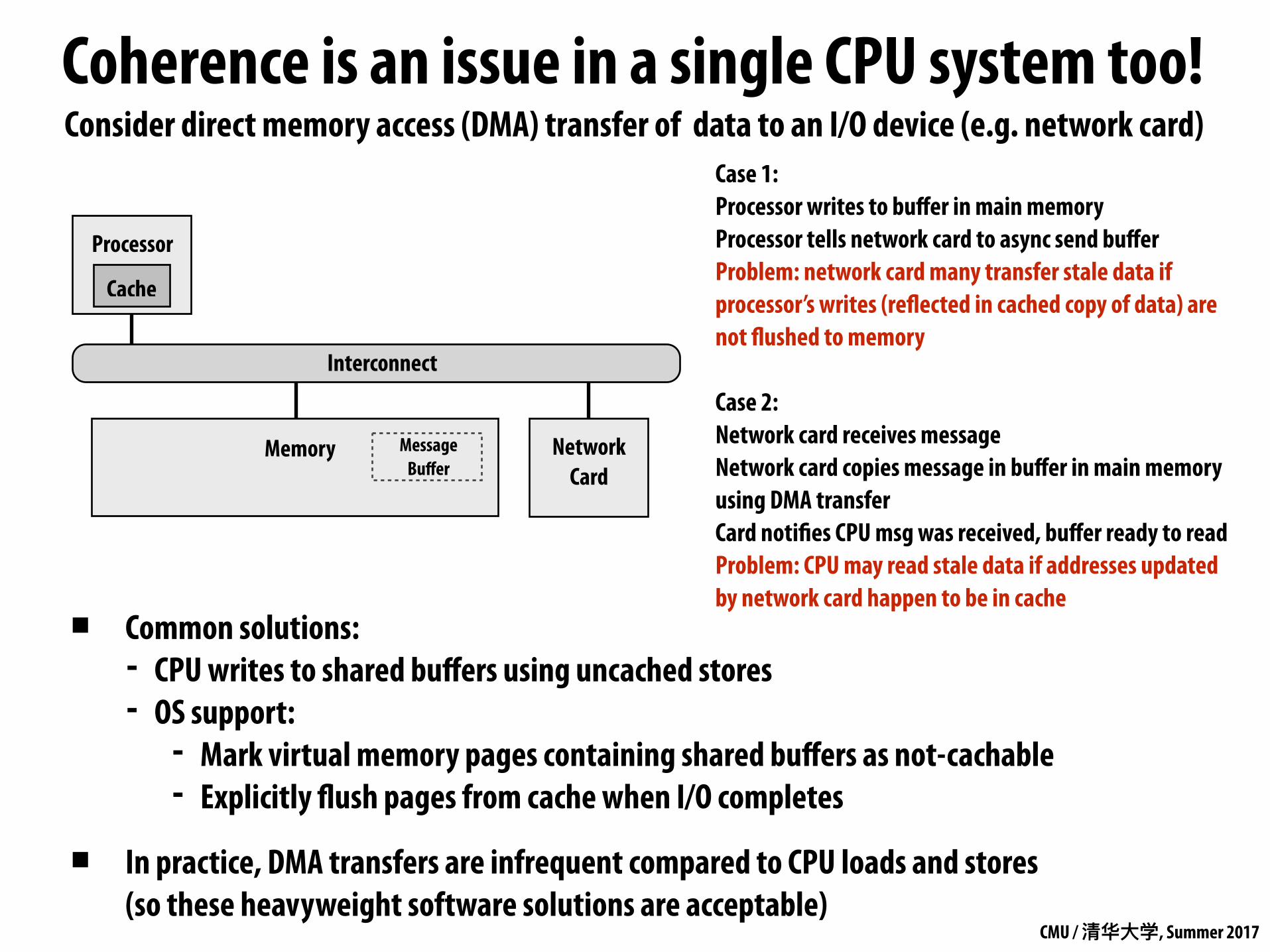
Coherence is an issue in a single CPU system too!
▪ Common solutions: - CPU writes to shared buffers using uncached stores - OS support:
- Mark virtual memory pages containing shared buffers as not-cachable - Explicitly flush pages from cache when I/O completes
▪ In practice, DMA transfers are infrequent compared to CPU loads and stores (so these heavyweight software solutions are acceptable)
Processor
Network Card
Interconnect
Memory
Cache
Case 1: Processor writes to buffer in main memory Processor tells network card to async send buffer Problem: network card many transfer stale data if processor’s writes (reflected in cached copy of data) are not flushed to memory
Case 2: Network card receives message Network card copies message in buffer in main memory using DMA transfer Card notifies CPU msg was received, buffer ready to read Problem: CPU may read stale data if addresses updated by network card happen to be in cache
Message Buffer
Consider direct memory access (DMA) transfer of data to an I/O device (e.g. network card)
CMU / 清华⼤大学, Summer 2017
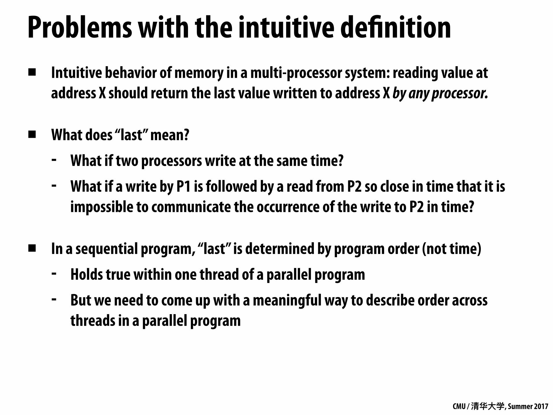
Problems with the intuitive definition▪ Intuitive behavior of memory in a multi-processor system: reading value at
address X should return the last value written to address X by any processor.
▪ What does “last” mean?
- What if two processors write at the same time?
- What if a write by P1 is followed by a read from P2 so close in time that it is impossible to communicate the occurrence of the write to P2 in time?
▪ In a sequential program, “last” is determined by program order (not time)
- Holds true within one thread of a parallel program
- But we need to come up with a meaningful way to describe order across threads in a parallel program
CMU / 清华⼤大学, Summer 2017
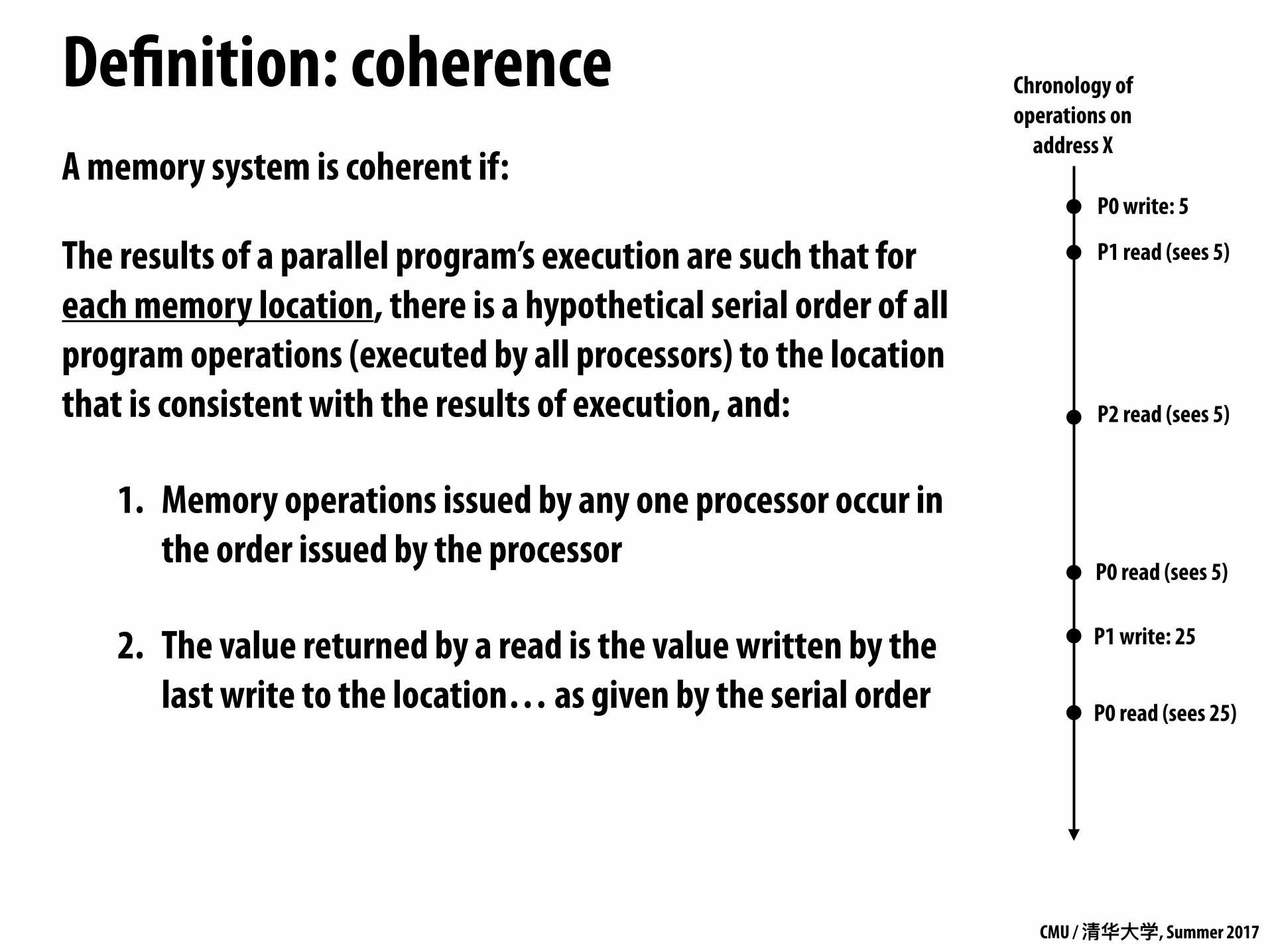
Definition: coherenceA memory system is coherent if:
The results of a parallel program’s execution are such that for each memory location, there is a hypothetical serial order of all program operations (executed by all processors) to the location that is consistent with the results of execution, and:
1. Memory operations issued by any one processor occur in the order issued by the processor
2. The value returned by a read is the value written by the last write to the location… as given by the serial order
Chronology of operations on
address X
P0 write: 5
P1 read (sees 5)
P2 read (sees 5)
P0 read (sees 5)
P1 write: 25
P0 read (sees 25)
CMU / 清华⼤大学, Summer 2017
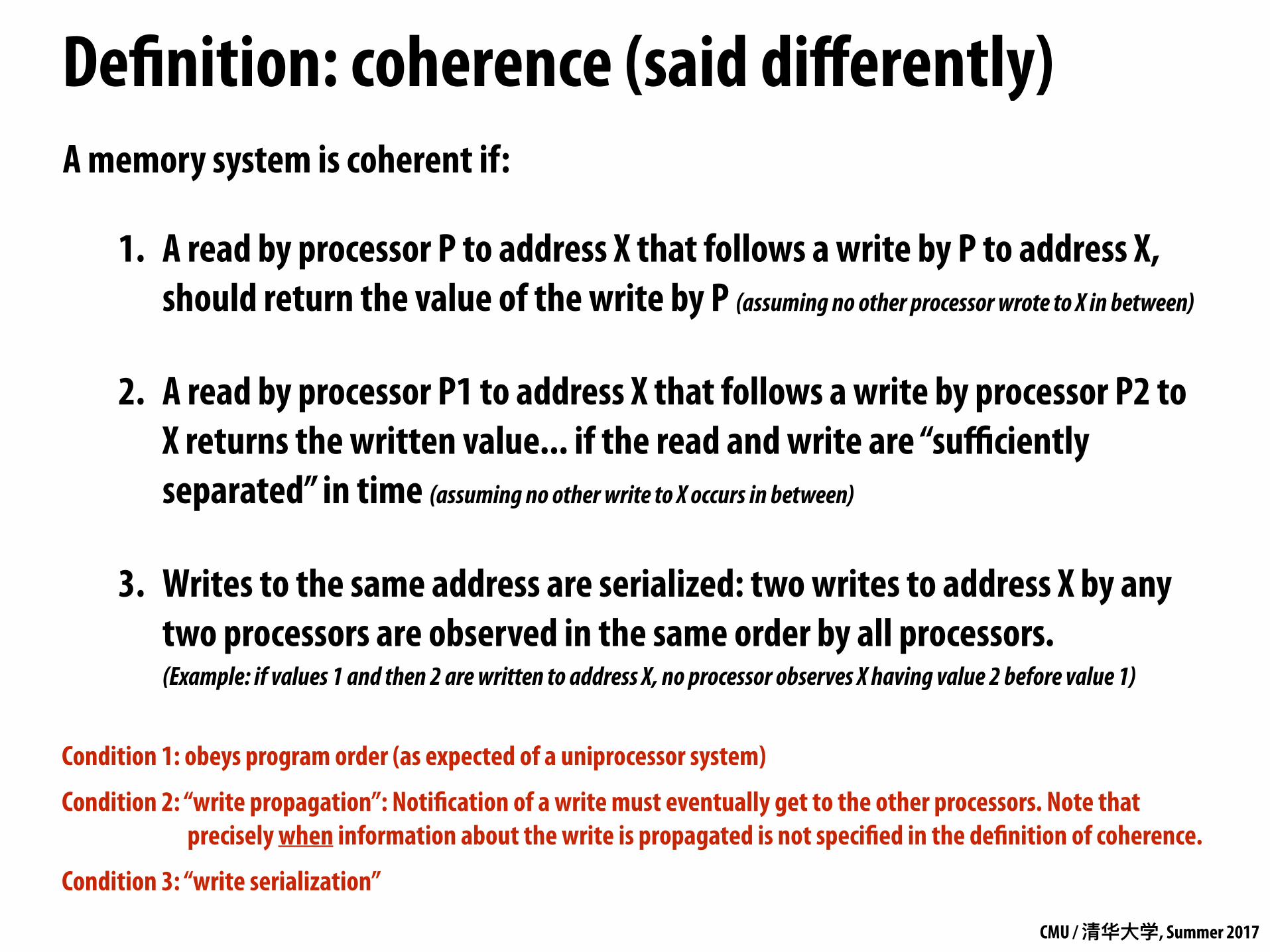
Definition: coherence (said differently)A memory system is coherent if:
1. A read by processor P to address X that follows a write by P to address X, should return the value of the write by P (assuming no other processor wrote to X in between)
2. A read by processor P1 to address X that follows a write by processor P2 to X returns the written value... if the read and write are “sufficiently separated” in time (assuming no other write to X occurs in between)
3. Writes to the same address are serialized: two writes to address X by any two processors are observed in the same order by all processors. (Example: if values 1 and then 2 are written to address X, no processor observes X having value 2 before value 1)
Condition 1: obeys program order (as expected of a uniprocessor system)
Condition 2: “write propagation”: Notification of a write must eventually get to the other processors. Note that precisely when information about the write is propagated is not specified in the definition of coherence.
Condition 3: “write serialization”
CMU / 清华⼤大学, Summer 2017
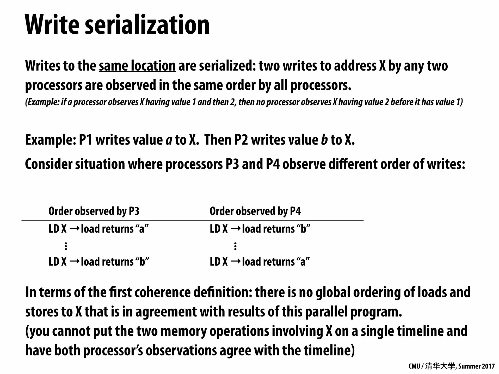
Write serializationWrites to the same location are serialized: two writes to address X by any two processors are observed in the same order by all processors. (Example: if a processor observes X having value 1 and then 2, then no processor observes X having value 2 before it has value 1)
Example: P1 writes value a to X. Then P2 writes value b to X.
Consider situation where processors P3 and P4 observe different order of writes:
Order observed by P3 LD X →load returns “a”
LD X →load returns “b”
... ...
Order observed by P4 LD X →load returns “b”
LD X →load returns “a”
In terms of the first coherence definition: there is no global ordering of loads and stores to X that is in agreement with results of this parallel program. (you cannot put the two memory operations involving X on a single timeline and have both processor’s observations agree with the timeline)

CMU / 清华⼤大学, Summer 2017
Implementing coherence ▪ Software-based solutions
- OS uses page-fault mechanism to propagate writes
- Can be used to implement memory coherence over clusters of workstations
- We won’t discuss these solutions
▪ Today’s topic: hardware-based solutions - “Snooping”-based coherence implementations
- Directory-based coherence implementations
CMU / 清华⼤大学, Summer 2017
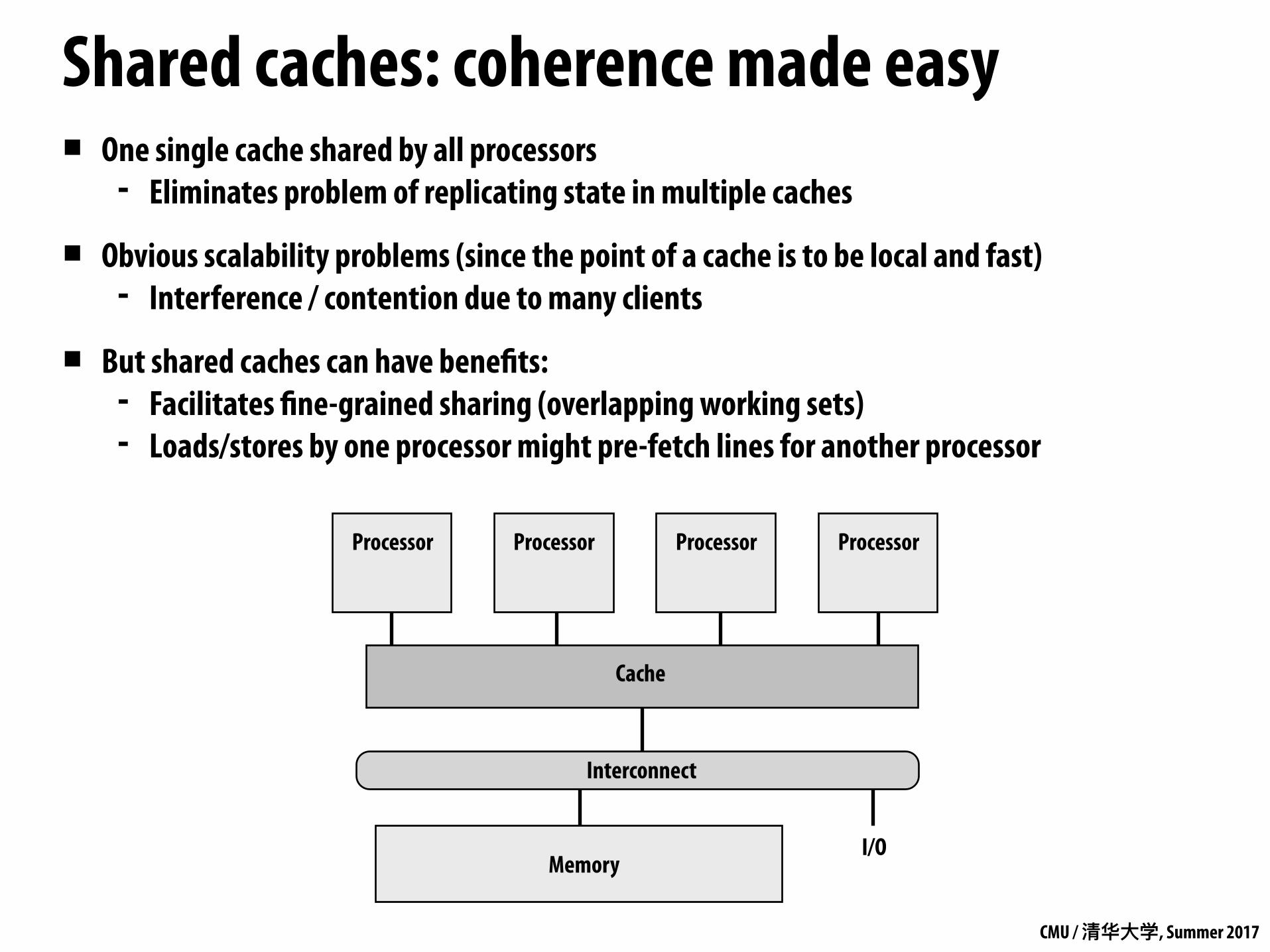
Shared caches: coherence made easy▪ One single cache shared by all processors
- Eliminates problem of replicating state in multiple caches
▪ Obvious scalability problems (since the point of a cache is to be local and fast) - Interference / contention due to many clients
▪ But shared caches can have benefits: - Facilitates fine-grained sharing (overlapping working sets) - Loads/stores by one processor might pre-fetch lines for another processor
Processor Processor Processor Processor
MemoryI/O
Cache
Interconnect

CMU / 清华⼤大学, Summer 2017
Snooping-based cache coherence
CMU / 清华⼤大学, Summer 2017
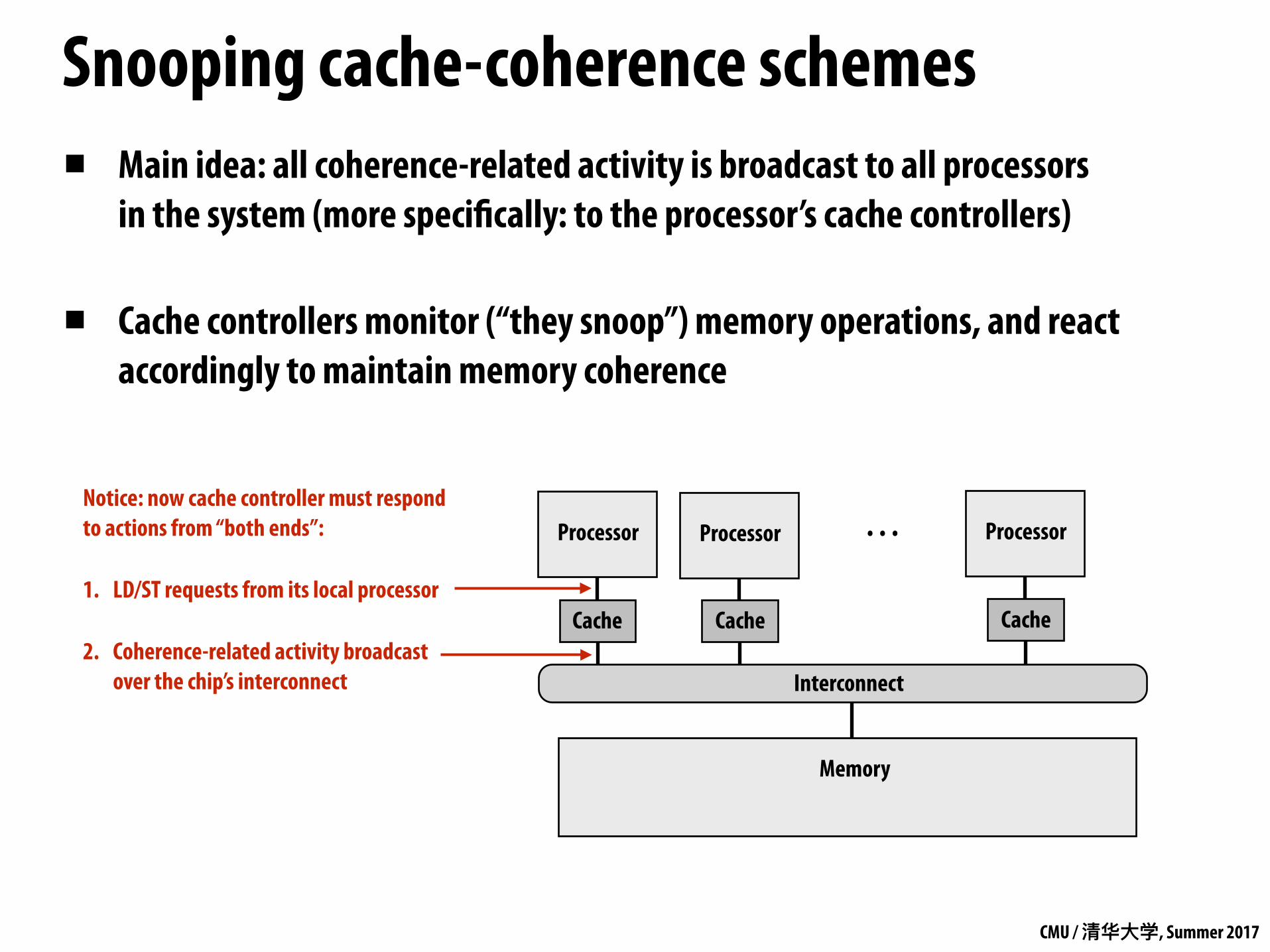
Snooping cache-coherence schemes▪ Main idea: all coherence-related activity is broadcast to all processors
in the system (more specifically: to the processor’s cache controllers)
▪ Cache controllers monitor (“they snoop”) memory operations, and react accordingly to maintain memory coherence
Processor
Interconnect
Memory
Cache
Processor
Cache
Processor
Cache
. . .Notice: now cache controller must respond to actions from “both ends”:
1. LD/ST requests from its local processor
2. Coherence-related activity broadcast over the chip’s interconnect

CMU / 清华⼤大学, Summer 2017
Very simple coherence implementationLet’s assume:
1. Write-through caches 2. Granularity of coherence is cache line
Upon write, cache controller broadcasts invalidation message
As a result, the next read from other processors will trigger cache miss (processor retrieves updated value from memory due to write-through policy)
P0 $ P1 $ mem location XAction
0
P1loadX 0 0 0
P0loadX 0 0
Cache
Processor P0
Memory
Cache
. . .
Interconnect
Processor P1
Interconnect activity
cachemissforX
cachemissforX
P0write100toX 100 100invalidationforX
P1loadX 100100 100cachemissforX
CMU / 清华⼤大学, Summer 2017
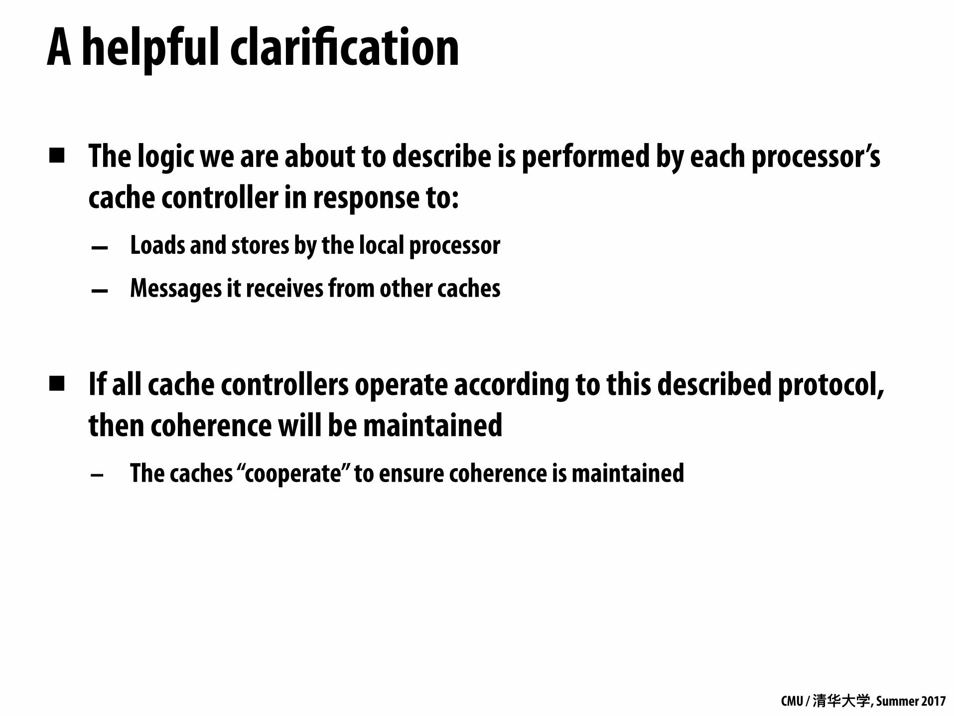
A helpful clarification
▪ The logic we are about to describe is performed by each processor’s cache controller in response to: - Loads and stores by the local processor
- Messages it receives from other caches
▪ If all cache controllers operate according to this described protocol, then coherence will be maintained - The caches “cooperate” to ensure coherence is maintained
CMU / 清华⼤大学, Summer 2017
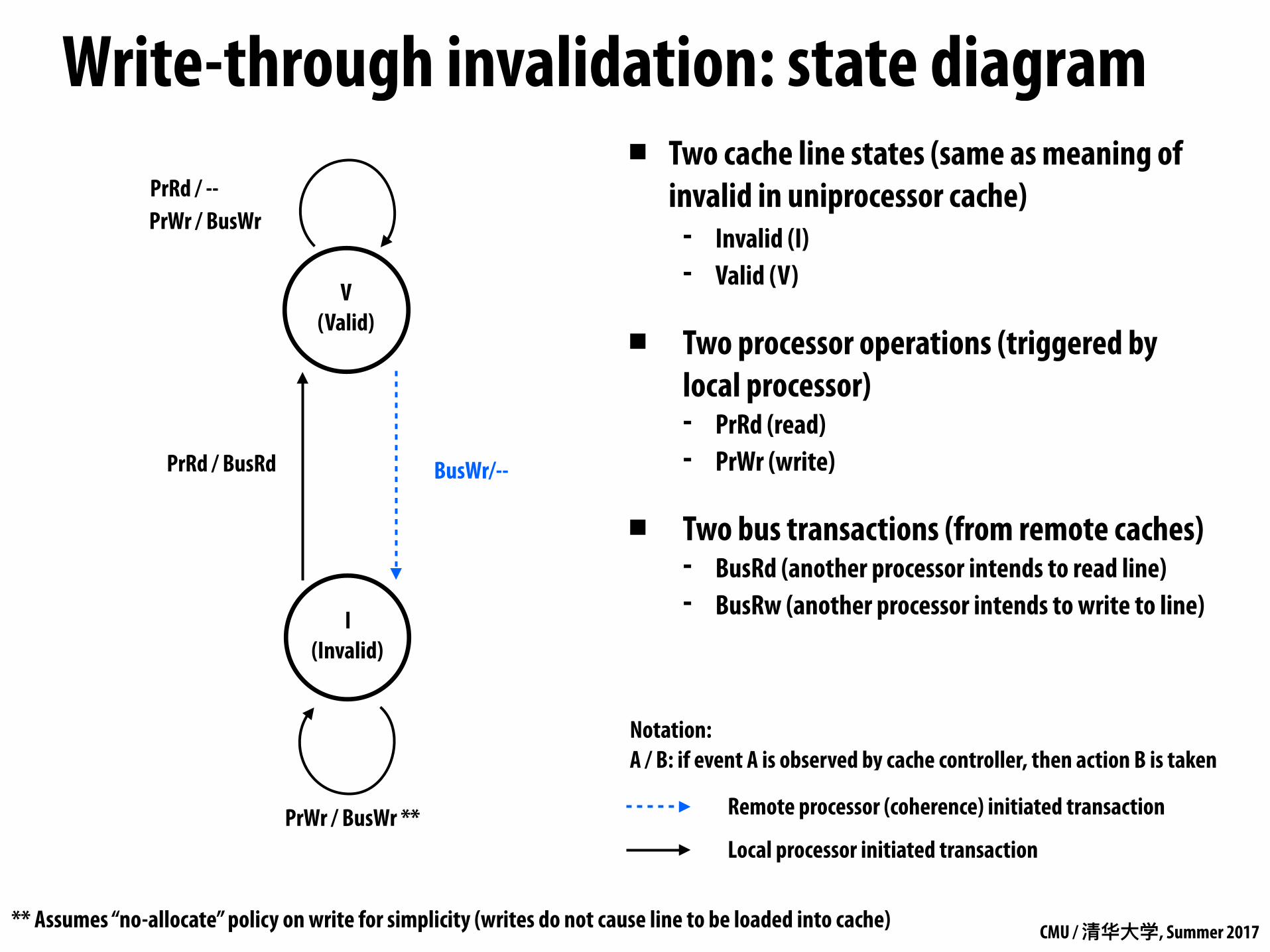
Write-through invalidation: state diagram
I (Invalid)
V (Valid)
PrRd / --
PrRd / BusRd
PrWr / BusWr **
PrWr / BusWr
BusWr/--
Notation: A / B: if event A is observed by cache controller, then action B is taken
** Assumes “no-allocate” policy on write for simplicity (writes do not cause line to be loaded into cache)
▪ Two cache line states (same as meaning of invalid in uniprocessor cache)
- Invalid (I) - Valid (V)
▪ Two processor operations (triggered by local processor) - PrRd (read) - PrWr (write)
▪ Two bus transactions (from remote caches) - BusRd (another processor intends to read line) - BusRw (another processor intends to write to line)
Remote processor (coherence) initiated transaction
Local processor initiated transaction
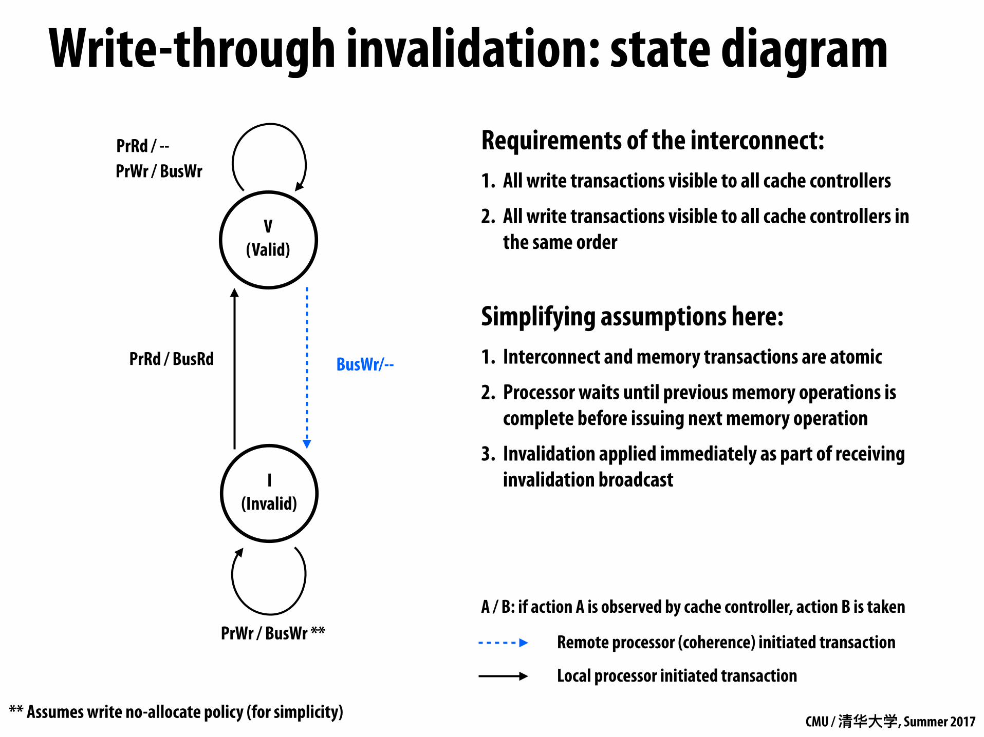
CMU / 清华⼤大学, Summer 2017
Write-through invalidation: state diagram
I (Invalid)
V (Valid)
PrRd / --
PrRd / BusRd
PrWr / BusWr **
PrWr / BusWr
BusWr/--
A / B: if action A is observed by cache controller, action B is taken
** Assumes write no-allocate policy (for simplicity)
Requirements of the interconnect: 1. All write transactions visible to all cache controllers
2. All write transactions visible to all cache controllers in the same order
Simplifying assumptions here: 1. Interconnect and memory transactions are atomic
2. Processor waits until previous memory operations is complete before issuing next memory operation
3. Invalidation applied immediately as part of receiving invalidation broadcast
Remote processor (coherence) initiated transaction
Local processor initiated transaction
CMU / 清华⼤大学, Summer 2017
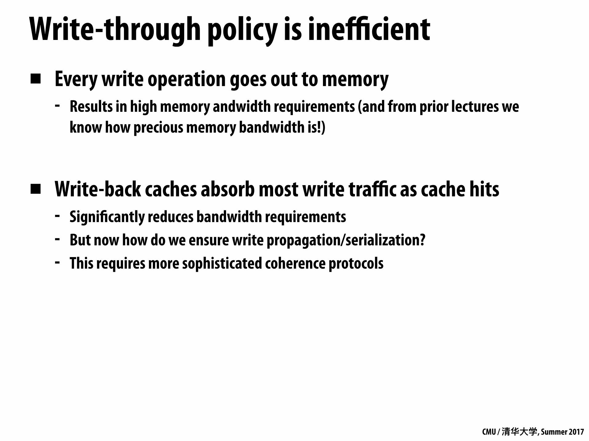
Write-through policy is inefficient▪ Every write operation goes out to memory
- Results in high memory andwidth requirements (and from prior lectures we know how precious memory bandwidth is!)
▪ Write-back caches absorb most write traffic as cache hits - Significantly reduces bandwidth requirements - But now how do we ensure write propagation/serialization? - This requires more sophisticated coherence protocols
CMU / 清华⼤大学, Summer 2017
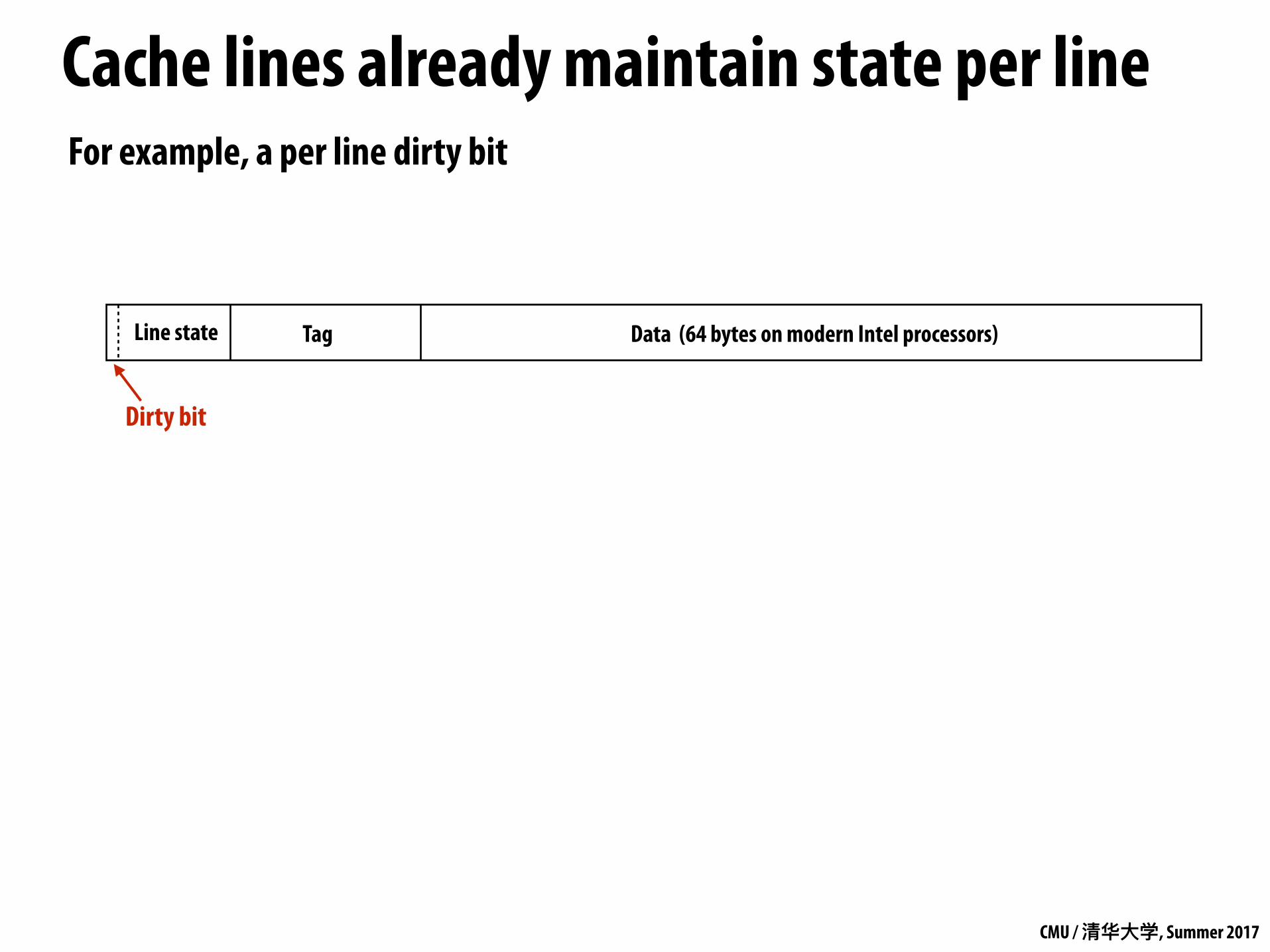
Cache lines already maintain state per line
Data (64 bytes on modern Intel processors)TagLine state
Dirty bit
For example, a per line dirty bit
CMU / 清华⼤大学, Summer 2017
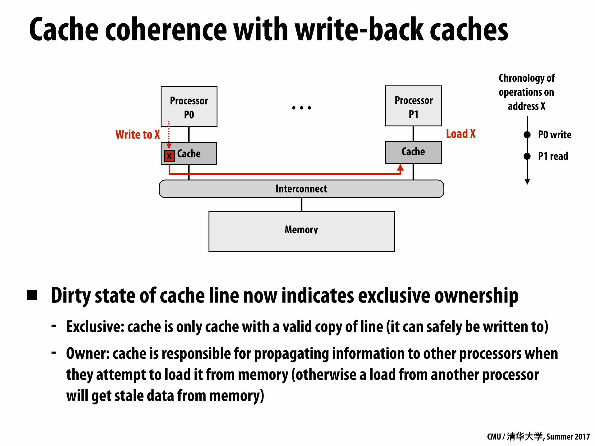
Cache coherence with write-back caches
Cache
Processor P0
Memory
Cache
. . .
Interconnect
Processor P1
X
Write to X Load X
▪ Dirty state of cache line now indicates exclusive ownership - Exclusive: cache is only cache with a valid copy of line (it can safely be written to)
- Owner: cache is responsible for propagating information to other processors when they attempt to load it from memory (otherwise a load from another processor will get stale data from memory)
Chronology of operations on
address X
P0 write
P1 read

CMU / 清华⼤大学, Summer 2017
Invalidation-based write-back protocolKey ideas:
▪ A line in the “exclusive” state can be modified without notifying the other caches
▪ Processor can only write to lines in the exclusive state - Need a way to tell other caches that processor wants exclusive access to the line - We accomplish this by sending all the other caches messages
▪ When cache controller snoops a request for exclusive access to a line it contains - It must invalidate the line in its own cache

CMU / 清华⼤大学, Summer 2017
MSI write-back invalidation protocol▪ Key tasks of protocol
- Ensuring processor obtains exclusive access for a write - Locating most recent copy of cache line’s data on cache miss
▪ Three cache line states - Invalid (I): same as meaning of invalid in uniprocessor cache - Shared (S): line valid in one or more caches - Modified (M): line valid in exactly one cache (a.k.a. “dirty” or “exclusive” state)
▪ Two processor operations (triggered by local CPU) - PrRd (read) - PrWr (write)
▪ Three coherence-related bus transactions (from remote caches) - BusRd: obtain copy of line with no intent to modify - BusRdX: obtain copy of line with intent to modify - flush: write dirty line out to memory

CMU / 清华⼤大学, Summer 2017
MSI state transition diagram *
S (Shared)
M (Modified)
PrRd / -- PrWr / --
PrRd / BusRd
BusRd / flush
Remote processor (coherence) initiated transaction
Local processor initiated transaction
A / B: if action A is observed by cache controller, action B is taken
I (Invalid)
PrWr / BusRdX
PrWr / BusRdX
PrRd / -- BusRdX / --
BusRdX / flush
BusRd / --
flush = flush dirty line to memory
* Remember, all caches are carrying out this logic independently to maintain coherence
CMU / 清华⼤大学, Summer 2017
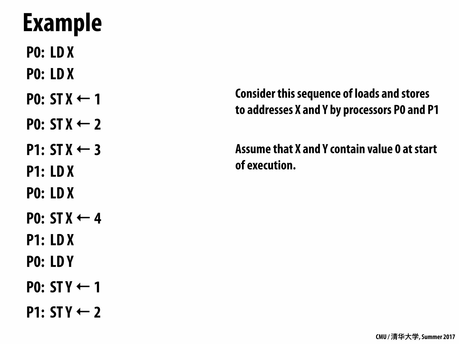
ExampleP0: LD X P0: LD X
P0: ST X ← 1
P0: ST X ← 2
P1: ST X ← 3 P1: LD X P0: LD X
P0: ST X ← 4 P1: LD X P0: LD Y
P0: ST Y ← 1
P1: ST Y ← 2
Consider this sequence of loads and stores to addresses X and Y by processors P0 and P1
Assume that X and Y contain value 0 at start of execution.
CMU / 清华⼤大学, Summer 2017
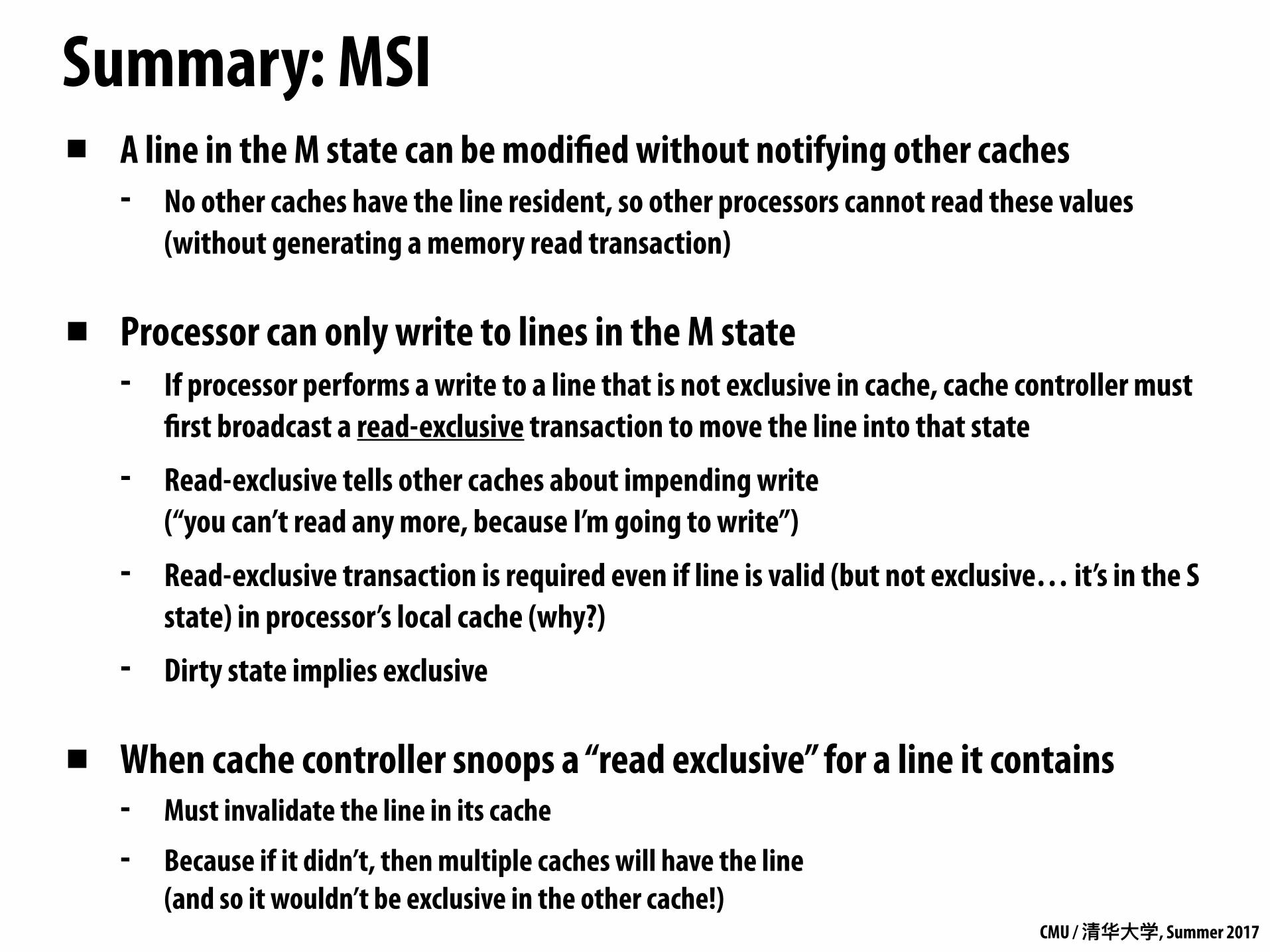
Summary: MSI▪ A line in the M state can be modified without notifying other caches
- No other caches have the line resident, so other processors cannot read these values (without generating a memory read transaction)
▪ Processor can only write to lines in the M state - If processor performs a write to a line that is not exclusive in cache, cache controller must
first broadcast a read-exclusive transaction to move the line into that state
- Read-exclusive tells other caches about impending write (“you can’t read any more, because I’m going to write”)
- Read-exclusive transaction is required even if line is valid (but not exclusive… it’s in the S state) in processor’s local cache (why?)
- Dirty state implies exclusive
▪ When cache controller snoops a “read exclusive” for a line it contains - Must invalidate the line in its cache
- Because if it didn’t, then multiple caches will have the line (and so it wouldn’t be exclusive in the other cache!)
CMU / 清华⼤大学, Summer 2017
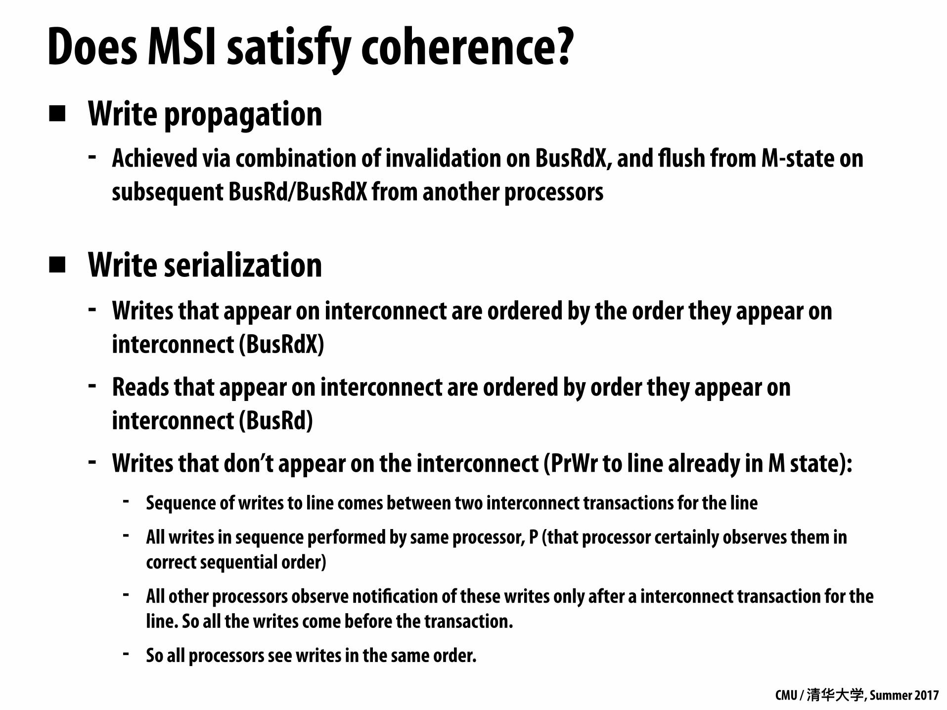
Does MSI satisfy coherence?▪ Write propagation
- Achieved via combination of invalidation on BusRdX, and flush from M-state on subsequent BusRd/BusRdX from another processors
▪ Write serialization - Writes that appear on interconnect are ordered by the order they appear on
interconnect (BusRdX)
- Reads that appear on interconnect are ordered by order they appear on interconnect (BusRd)
- Writes that don’t appear on the interconnect (PrWr to line already in M state): - Sequence of writes to line comes between two interconnect transactions for the line
- All writes in sequence performed by same processor, P (that processor certainly observes them in correct sequential order)
- All other processors observe notification of these writes only after a interconnect transaction for the line. So all the writes come before the transaction.
- So all processors see writes in the same order.
CMU / 清华⼤大学, Summer 2017
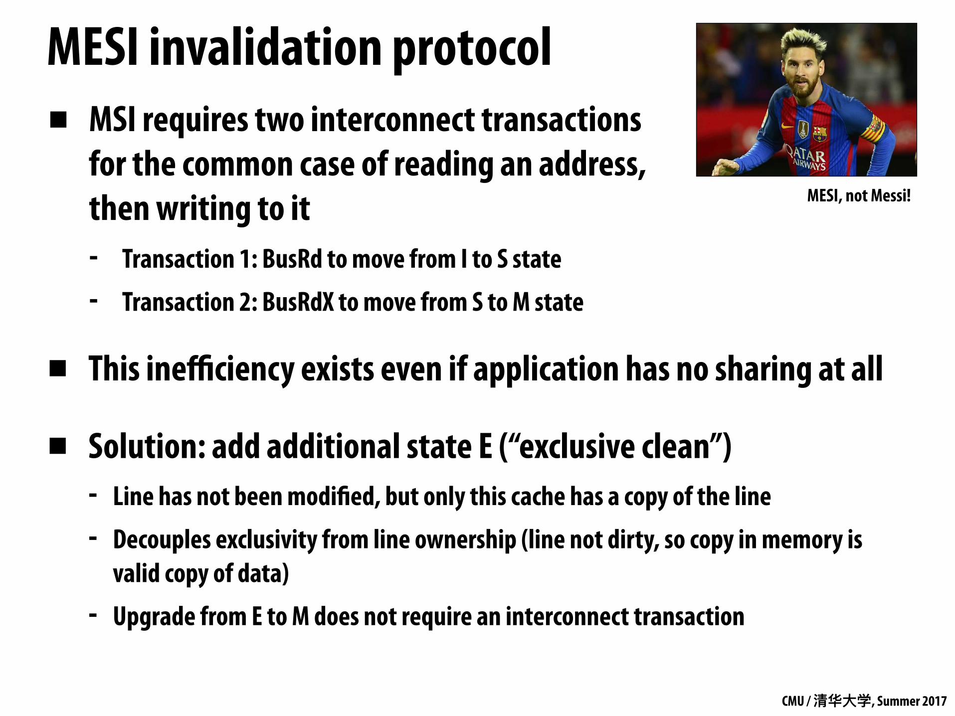
MESI invalidation protocol
▪ This inefficiency exists even if application has no sharing at all
▪ Solution: add additional state E (“exclusive clean”) - Line has not been modified, but only this cache has a copy of the line
- Decouples exclusivity from line ownership (line not dirty, so copy in memory is valid copy of data)
- Upgrade from E to M does not require an interconnect transaction
MESI, not Messi!
▪ MSI requires two interconnect transactions for the common case of reading an address, then writing to it - Transaction 1: BusRd to move from I to S state
- Transaction 2: BusRdX to move from S to M state
CMU / 清华⼤大学, Summer 2017
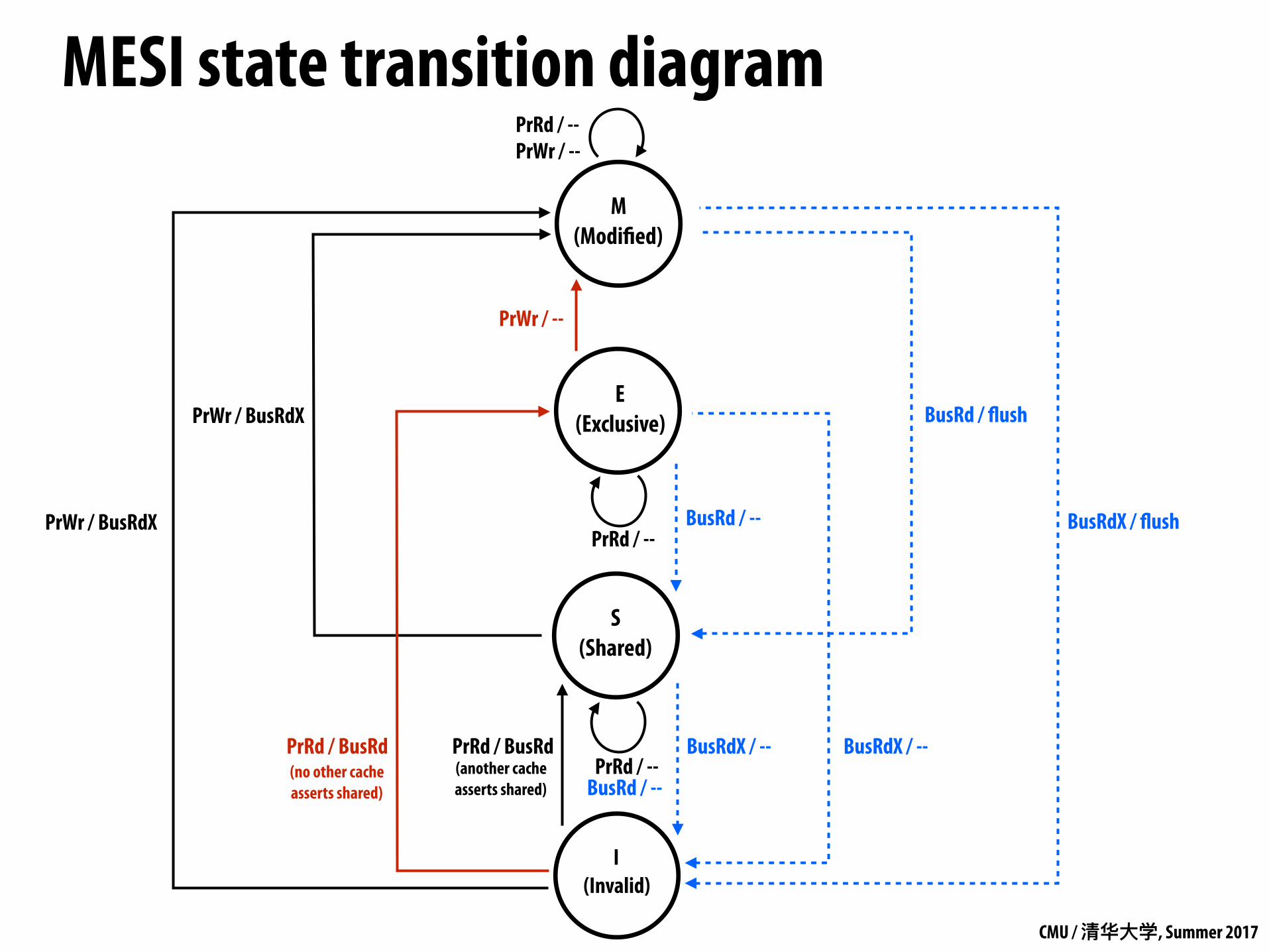
MESI state transition diagram
E (Exclusive)
M (Modified)
PrRd / -- PrWr / --
PrWr / BusRdX BusRd / flush
I (Invalid)
PrWr / BusRdX
PrWr / --
PrRd / --BusRdX / --
BusRdX / flush
BusRd / --
S (Shared)
PrRd / --
PrRd / BusRd (no other cache asserts shared)
PrRd / BusRd
BusRd / --
BusRdX / --(another cache asserts shared)
CMU / 清华⼤大学, Summer 2017
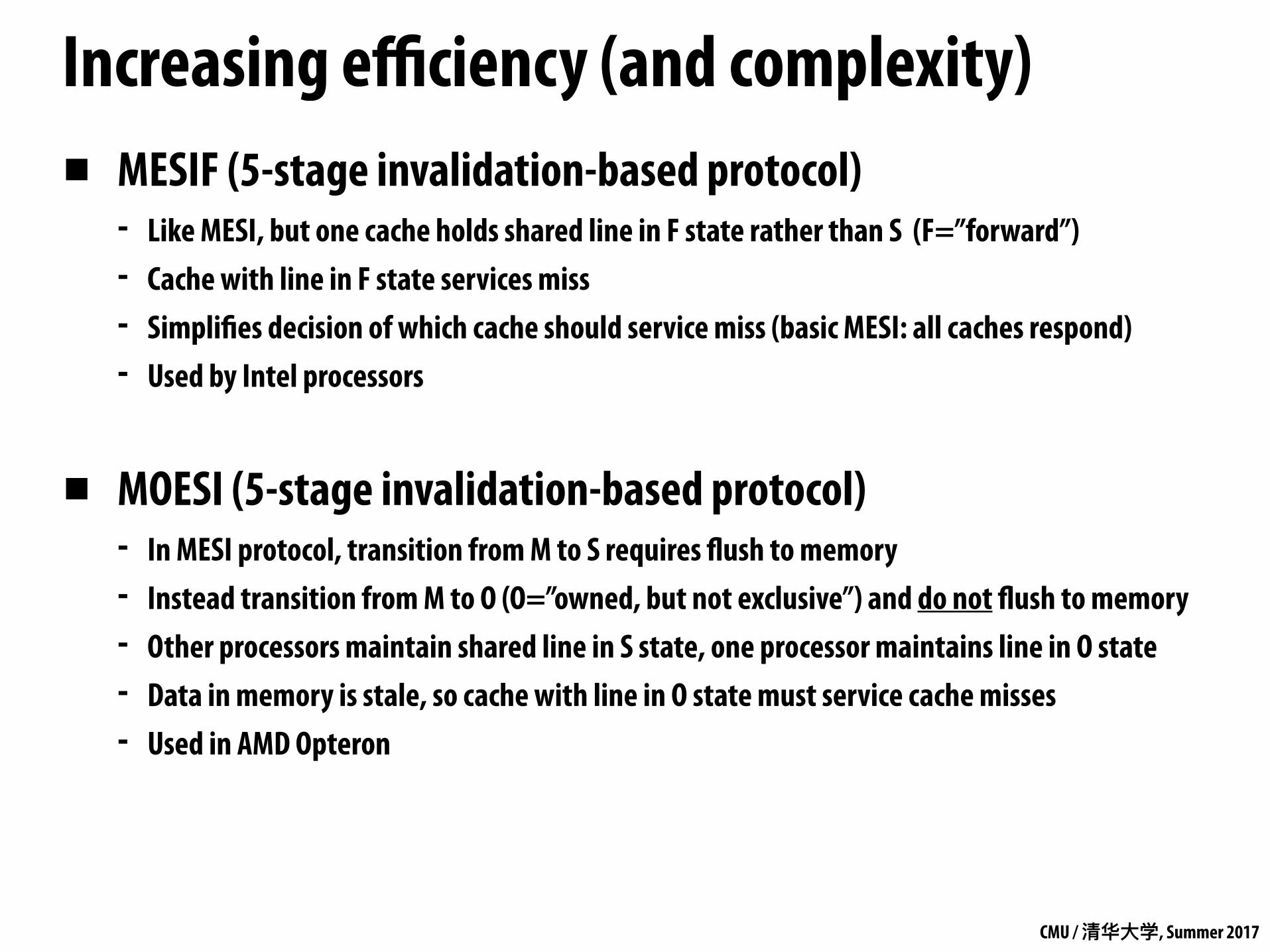
Increasing efficiency (and complexity)▪ MESIF (5-stage invalidation-based protocol)
- Like MESI, but one cache holds shared line in F state rather than S (F=”forward”) - Cache with line in F state services miss - Simplifies decision of which cache should service miss (basic MESI: all caches respond) - Used by Intel processors
▪ MOESI (5-stage invalidation-based protocol) - In MESI protocol, transition from M to S requires flush to memory - Instead transition from M to O (O=”owned, but not exclusive”) and do not flush to memory - Other processors maintain shared line in S state, one processor maintains line in O state - Data in memory is stale, so cache with line in O state must service cache misses - Used in AMD Opteron

CMU / 清华⼤大学, Summer 2017
Reality: multi-level cache hierarchies
Core
L1 Data Cache
L2 Cache
Shared L3 Cache (One bank per core)
Ring Interconnect
Core
L1 Data Cache
L2 Cache
Core
L1 Data Cache
L2 Cache
Core
L1 Data Cache
L2 Cache
Recall Intel Core i7 hierarchy
▪ Challenge: changes made to data at first level cache may not be visible to second level cache controller than snoops the interconnect.
▪ How might snooping work for a cache hierarchy?
1. All caches snoop interconnect independently? (inefficient)
2. Maintain “inclusion”
CMU / 清华⼤大学, Summer 2017
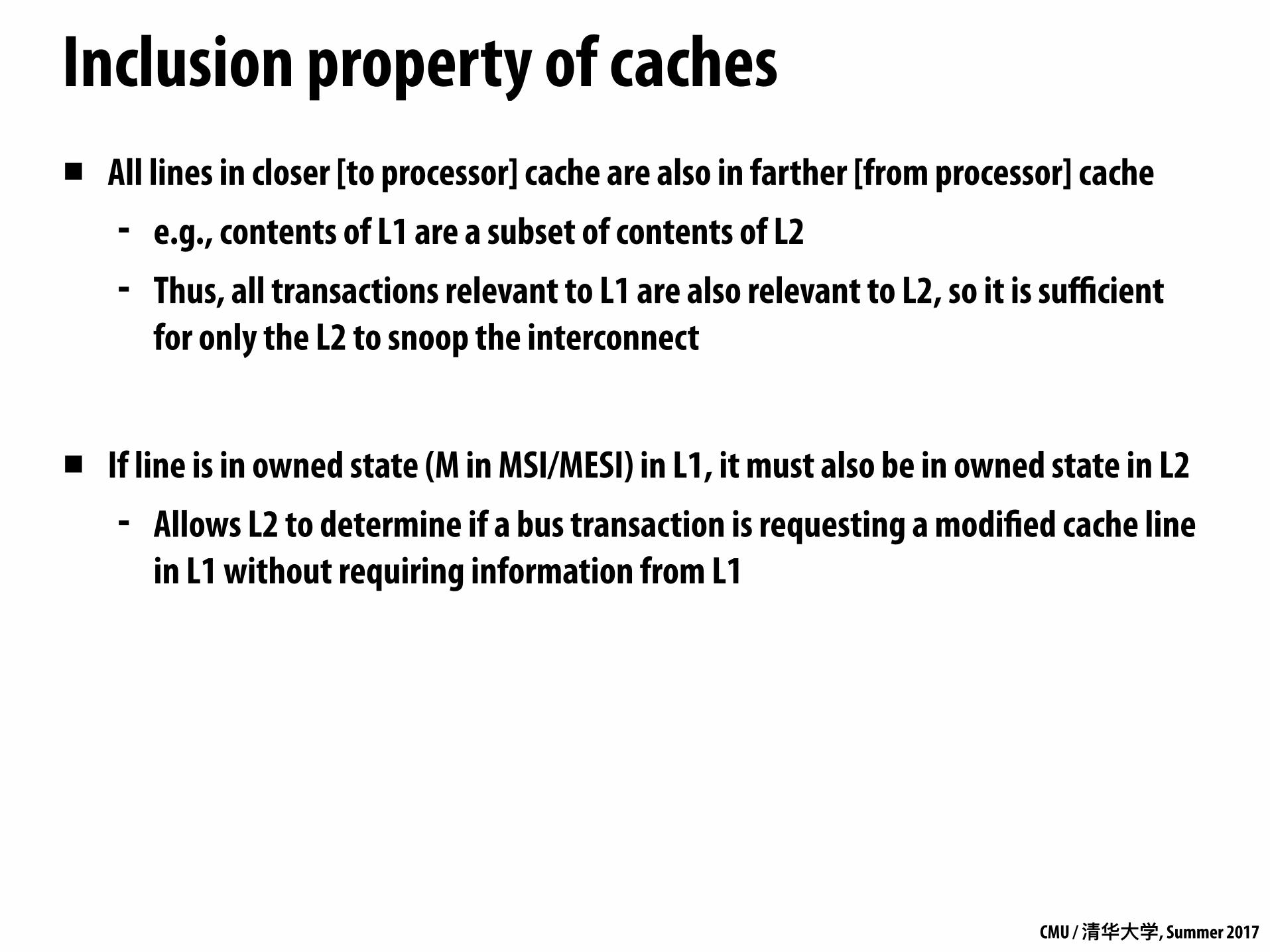
Inclusion property of caches▪ All lines in closer [to processor] cache are also in farther [from processor] cache
- e.g., contents of L1 are a subset of contents of L2
- Thus, all transactions relevant to L1 are also relevant to L2, so it is sufficient for only the L2 to snoop the interconnect
▪ If line is in owned state (M in MSI/MESI) in L1, it must also be in owned state in L2
- Allows L2 to determine if a bus transaction is requesting a modified cache line in L1 without requiring information from L1

CMU / 清华⼤大学, Summer 2017
Is inclusion maintained automatically if L2 is larger than L1?▪ Consider this example:
- Let L2 cache be twice as large as L1 cache - Let L1 and L2 have the same line size, are 2-way set associative, and use LRU replacement policy - Let A, B, C map to the same set of the L1 cache
A
B
A
BL2
Cache
L1 Cache
Processor accesses A (L1+L2 miss)
✘
✘
No!
Set 0 Set 1
Set 0 Set 1
Set 2 Set 3
Processor accesses B (L1+L2 miss).
Processor accesses A many times (all L1 hits).
Processor now accesses C, triggering an L1 and L2 miss. L1 and L2 might choose to evict different lines, because the access histories differ.
As a result, inclusion no longer holds!

CMU / 清华⼤大学, Summer 2017
Maintaining inclusion: handling invalidations
L1 Cache
L2 Cache
Processor
Interconnect
BusRdX / --
When line X is invalidated in L2 cache due to BusRdX from another cache.
Must also invalidate line X in L1
Invalidate
X
X
✘
✘
“in L1” bitOne solution: each L2 line contains an additional state bit indicating if line also exists in L1
This bit tells the L2 invalidations of the cache line due to coherence traffic need to be propagated to L1.
CMU / 清华⼤大学, Summer 2017
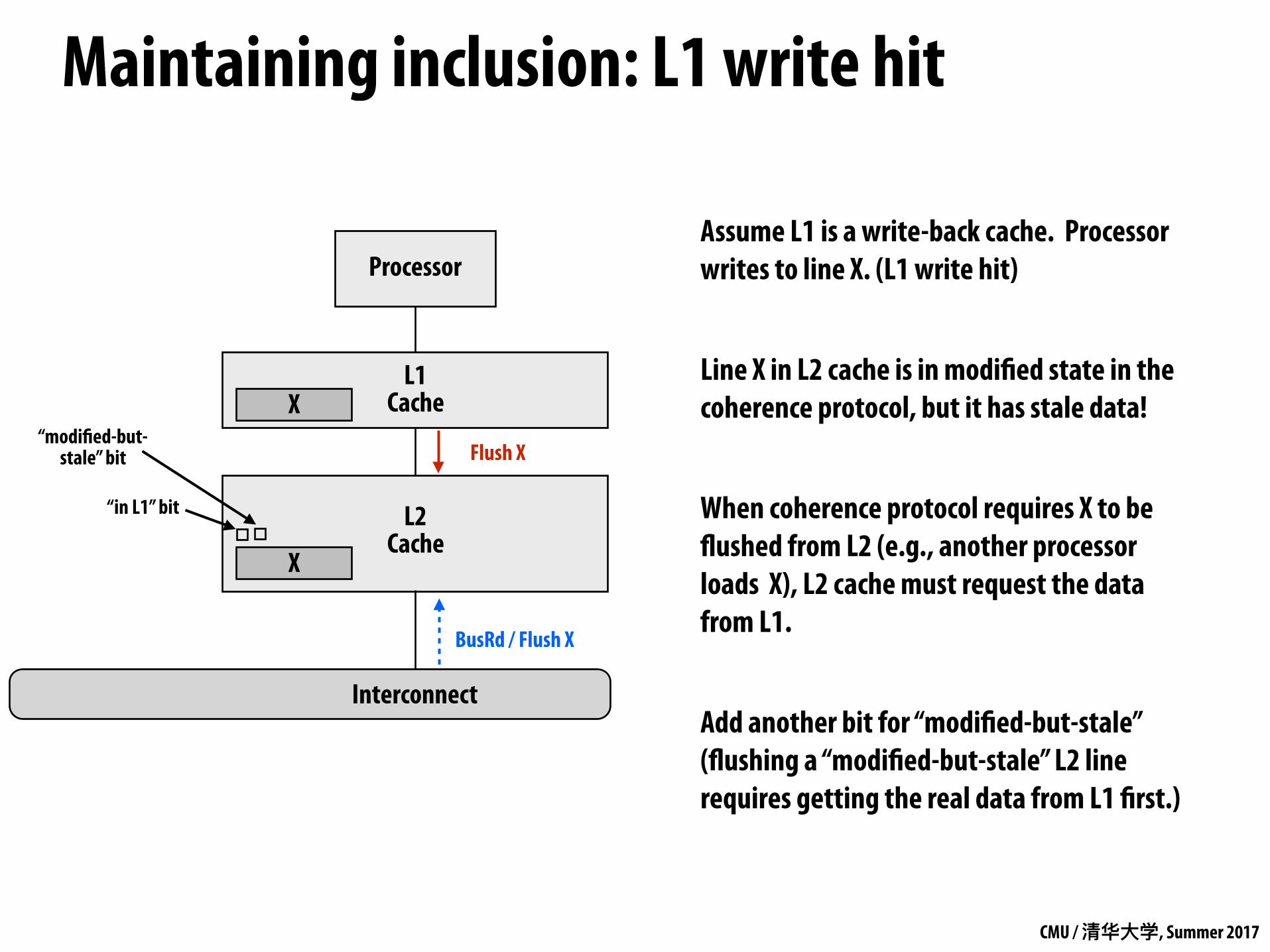
Maintaining inclusion: L1 write hit
L1 Cache
L2 Cache
Processor
Interconnect
Assume L1 is a write-back cache. Processor writes to line X. (L1 write hit)
Line X in L2 cache is in modified state in the coherence protocol, but it has stale data!
When coherence protocol requires X to be flushed from L2 (e.g., another processor loads X), L2 cache must request the data from L1.
Add another bit for “modified-but-stale” (flushing a “modified-but-stale” L2 line requires getting the real data from L1 first.)
Flush X
X
X
“in L1” bit
“modified-but-stale” bit
BusRd / Flush X
CMU / 清华⼤大学, Summer 2017
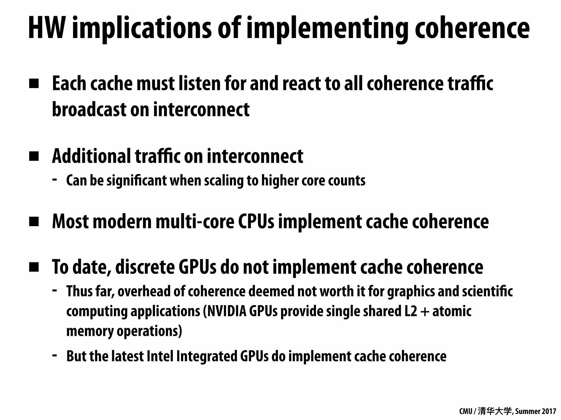
HW implications of implementing coherence
▪ Each cache must listen for and react to all coherence traffic broadcast on interconnect
▪ Additional traffic on interconnect - Can be significant when scaling to higher core counts
▪ Most modern multi-core CPUs implement cache coherence
▪ To date, discrete GPUs do not implement cache coherence - Thus far, overhead of coherence deemed not worth it for graphics and scientific
computing applications (NVIDIA GPUs provide single shared L2 + atomic memory operations)
- But the latest Intel Integrated GPUs do implement cache coherence
CMU / 清华⼤大学, Summer 2017
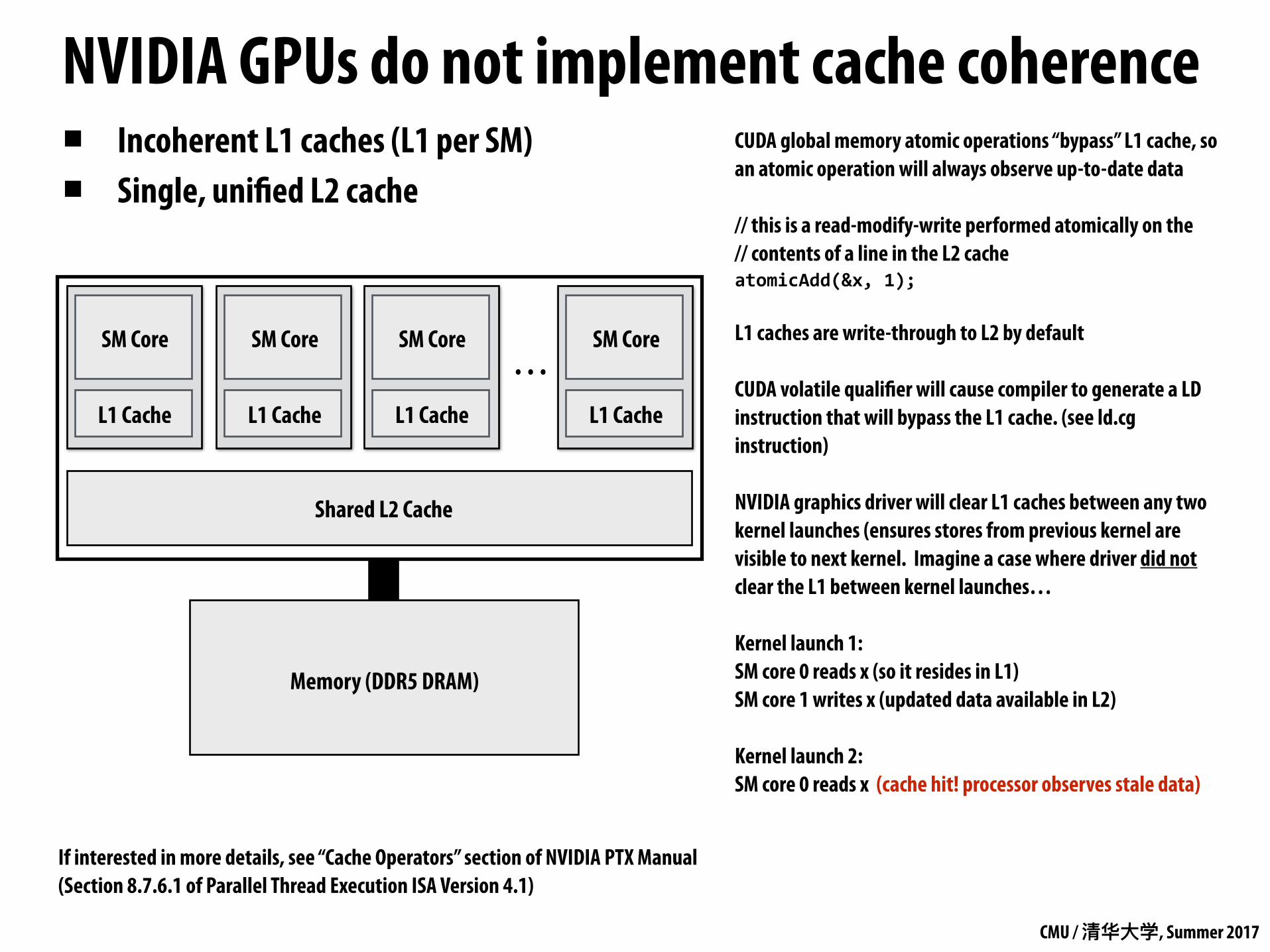
NVIDIA GPUs do not implement cache coherence ▪ Incoherent L1 caches (L1 per SM) ▪ Single, unified L2 cache
Memory (DDR5 DRAM)
Shared L2 Cache
L1 Cache
SM Core
L1 Cache
SM Core
L1 Cache
SM Core
L1 Cache
SM Core. . .
CUDA global memory atomic operations “bypass” L1 cache, so an atomic operation will always observe up-to-date data
// this is a read-modify-write performed atomically on the // contents of a line in the L2 cache atomicAdd(&x,1);
L1 caches are write-through to L2 by default
CUDA volatile qualifier will cause compiler to generate a LD instruction that will bypass the L1 cache. (see ld.cg instruction)
NVIDIA graphics driver will clear L1 caches between any two kernel launches (ensures stores from previous kernel are visible to next kernel. Imagine a case where driver did not clear the L1 between kernel launches…
Kernel launch 1: SM core 0 reads x (so it resides in L1) SM core 1 writes x (updated data available in L2)
Kernel launch 2: SM core 0 reads x (cache hit! processor observes stale data)
If interested in more details, see “Cache Operators” section of NVIDIA PTX Manual (Section 8.7.6.1 of Parallel Thread Execution ISA Version 4.1)
CMU / 清华⼤大学, Summer 2017
Implications of cache coherence to the programmer

CMU / 清华⼤大学, Summer 2017
Artifactual communication via false sharing
What is the potential performance problem with this code? //allocateper-threadvariableforlocalper-threadaccumulation
intmyPerThreadCounter[NUM_THREADS];
Why is this better? //allocateperthreadvariableforlocalaccumulation
structPerThreadState{
intmyPerThreadCounter;
charpadding[CACHE_LINE_SIZE-sizeof(int)];
};
PerThreadStatemyPerThreadCounter[NUM_THREADS];
CMU / 清华⼤大学, Summer 2017
Demo: false sharingvoid*worker(void*arg){volatileint*counter=(int*)arg;
for(inti=0;i<MANY_ITERATIONS;i++)(*counter)++;
returnNULL;}
voidtest1(intnum_threads){
pthread_tthreads[MAX_THREADS];intcounter[MAX_THREADS];
for(inti=0;i<num_threads;i++)pthread_create(&threads[i],NULL,&worker,&counter[i]);
for(inti=0;i<num_threads;i++)pthread_join(threads[i],NULL);}
voidtest2(intnum_threads){
pthread_tthreads[MAX_THREADS];padded_tcounter[MAX_THREADS];
for(inti=0;i<num_threads;i++)pthread_create(&threads[i],NULL,&worker,&(counter[i].counter));
for(inti=0;i<num_threads;i++)pthread_join(threads[i],NULL);}
structpadded_t{intcounter;charpadding[CACHE_LINE_SIZE-sizeof(int)];};
Execution time with num_threads=8 on 4-core system: 7.2 sec
Execution time with num_threads=8 on 4-core system: 3.06 sec
threads update a per-thread counter many times
CMU / 清华⼤大学, Summer 2017
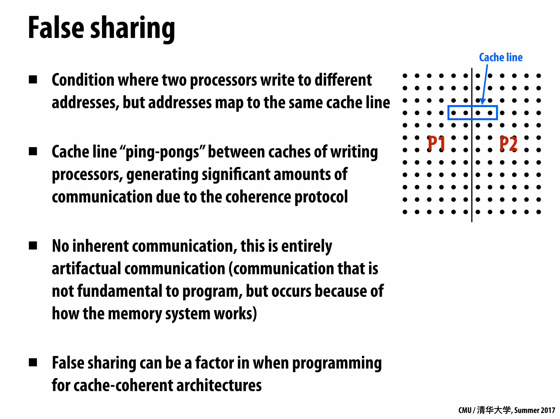
False sharing
▪ Condition where two processors write to different addresses, but addresses map to the same cache line
▪ Cache line “ping-pongs” between caches of writing processors, generating significant amounts of communication due to the coherence protocol
▪ No inherent communication, this is entirely artifactual communication (communication that is not fundamental to program, but occurs because of how the memory system works)
▪ False sharing can be a factor in when programming for cache-coherent architectures
P1 P2
Cache line
CMU / 清华⼤大学, Summer 2017
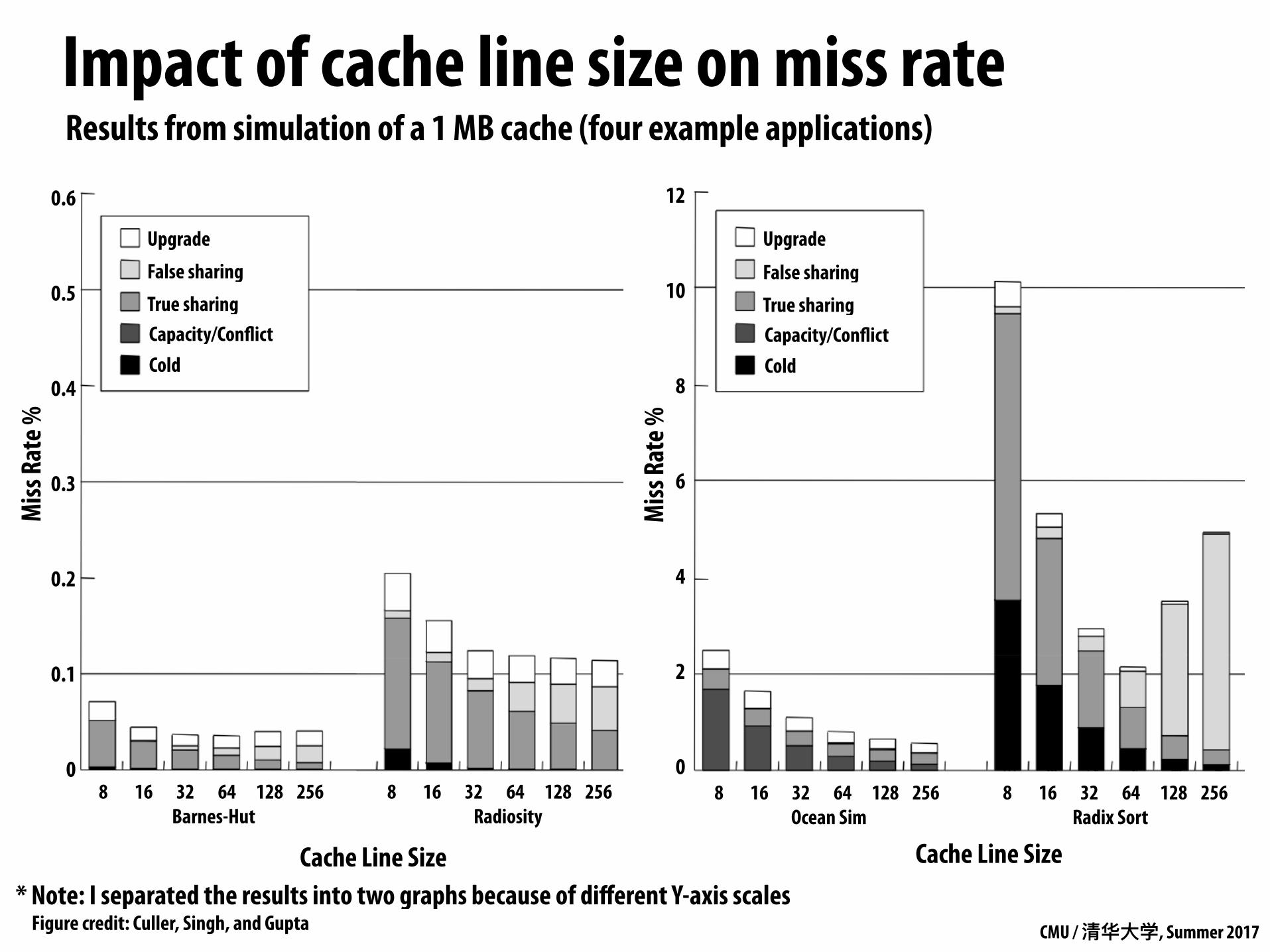
Impact of cache line size on miss rateM
iss R
ate %
0.6
0.5
0.4
0.3
0.2
0.1
0
Upgrade
False sharing
True sharingCapacity/ConflictCold
8 16 32 64 128 256 8 16 32 64 128 256Barnes-Hut Radiosity
Cache Line Size
Miss
Rat
e %
12
10
8
6
4
2
0
Upgrade
False sharing
True sharingCapacity/ConflictCold
8 16 32 64 128 256 8 16 32 64 128 256Ocean Sim Radix Sort
Cache Line Size
Results from simulation of a 1 MB cache (four example applications)
* Note: I separated the results into two graphs because of different Y-axis scalesFigure credit: Culler, Singh, and Gupta
CMU / 清华⼤大学, Summer 2017
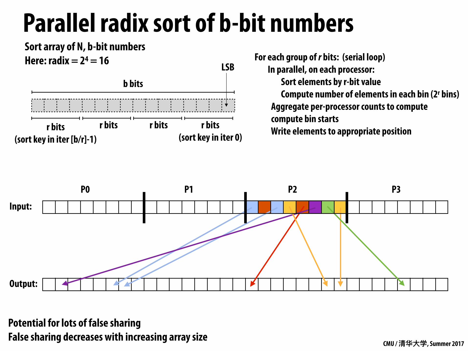
Parallel radix sort of b-bit numbers
Input:
P0 P1 P2 P3
Output:
Sort array of N, b-bit numbers Here: radix = 24 = 16
b bits
r bits (sort key in iter 0)
r bitsr bitsr bits (sort key in iter [b/r]-1)
For each group of r bits: (serial loop) In parallel, on each processor: Sort elements by r-bit value Compute number of elements in each bin (2r bins) Aggregate per-processor counts to compute compute bin starts Write elements to appropriate position
LSB
Potential for lots of false sharing False sharing decreases with increasing array size
CMU / 清华⼤大学, Summer 2017
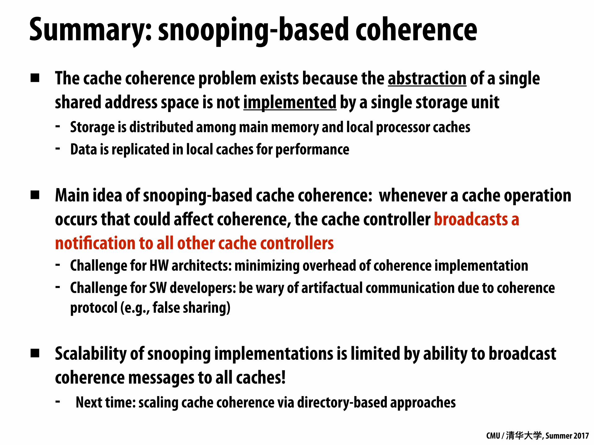
Summary: snooping-based coherence▪ The cache coherence problem exists because the abstraction of a single
shared address space is not implemented by a single storage unit - Storage is distributed among main memory and local processor caches - Data is replicated in local caches for performance
▪ Main idea of snooping-based cache coherence: whenever a cache operation occurs that could affect coherence, the cache controller broadcasts a notification to all other cache controllers - Challenge for HW architects: minimizing overhead of coherence implementation - Challenge for SW developers: be wary of artifactual communication due to coherence
protocol (e.g., false sharing)
▪ Scalability of snooping implementations is limited by ability to broadcast coherence messages to all caches! - Next time: scaling cache coherence via directory-based approaches

CMU / 清华⼤大学, Summer 2017
Directory-based cache coherence
CMU / 清华⼤大学, Summer 2017
What you should know▪ What limits the scalability of snooping-based approaches to
cache coherence?
▪ How does a directory-based scheme avoid these problems?
▪ How can the storage overhead of the directory structure be reduced?
CMU / 清华⼤大学, Summer 2017
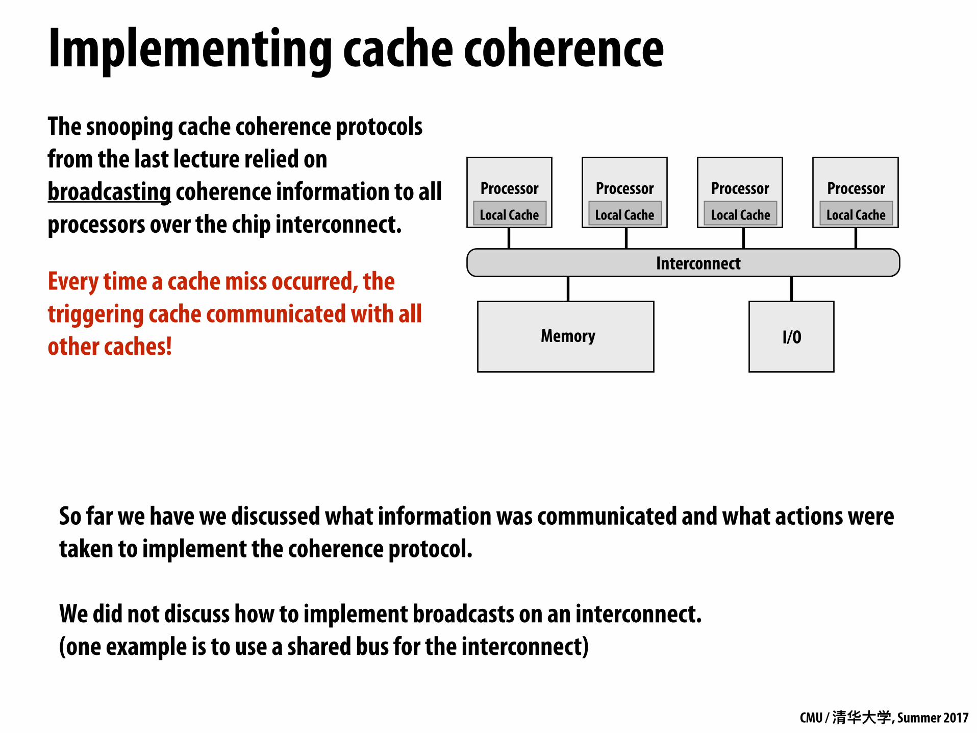
Implementing cache coherence
ProcessorLocal Cache
ProcessorLocal Cache
ProcessorLocal Cache
ProcessorLocal Cache
Interconnect
Memory I/O
The snooping cache coherence protocols from the last lecture relied on broadcasting coherence information to all processors over the chip interconnect.
Every time a cache miss occurred, the triggering cache communicated with all other caches!
So far we have we discussed what information was communicated and what actions were taken to implement the coherence protocol.
We did not discuss how to implement broadcasts on an interconnect. (one example is to use a shared bus for the interconnect)

CMU / 清华⼤大学, Summer 2017
Problem: scaling cache coherence to larger machines
Processor
Local Cache
Memory
Processor
Local Cache
Memory
Processor
Local Cache
Memory
Processor
Local Cache
Memory
Interconnect
Idea: locating regions of memory near the processors increases scalability: it yields higher aggregate bandwidth and reduced latency (especially when there is locality in the application)
But... efficiency of NUMA system does little good if the coherence protocol can’t also be scaled!
Consider this case: processor accesses its local memory (which is good), but to ensure memory coherence it still must broadcast to all other processors it is doing so (which is bad) SGI UV 1000 (4,096 coherent cores)
CMU / 清华⼤大学, Summer 2017
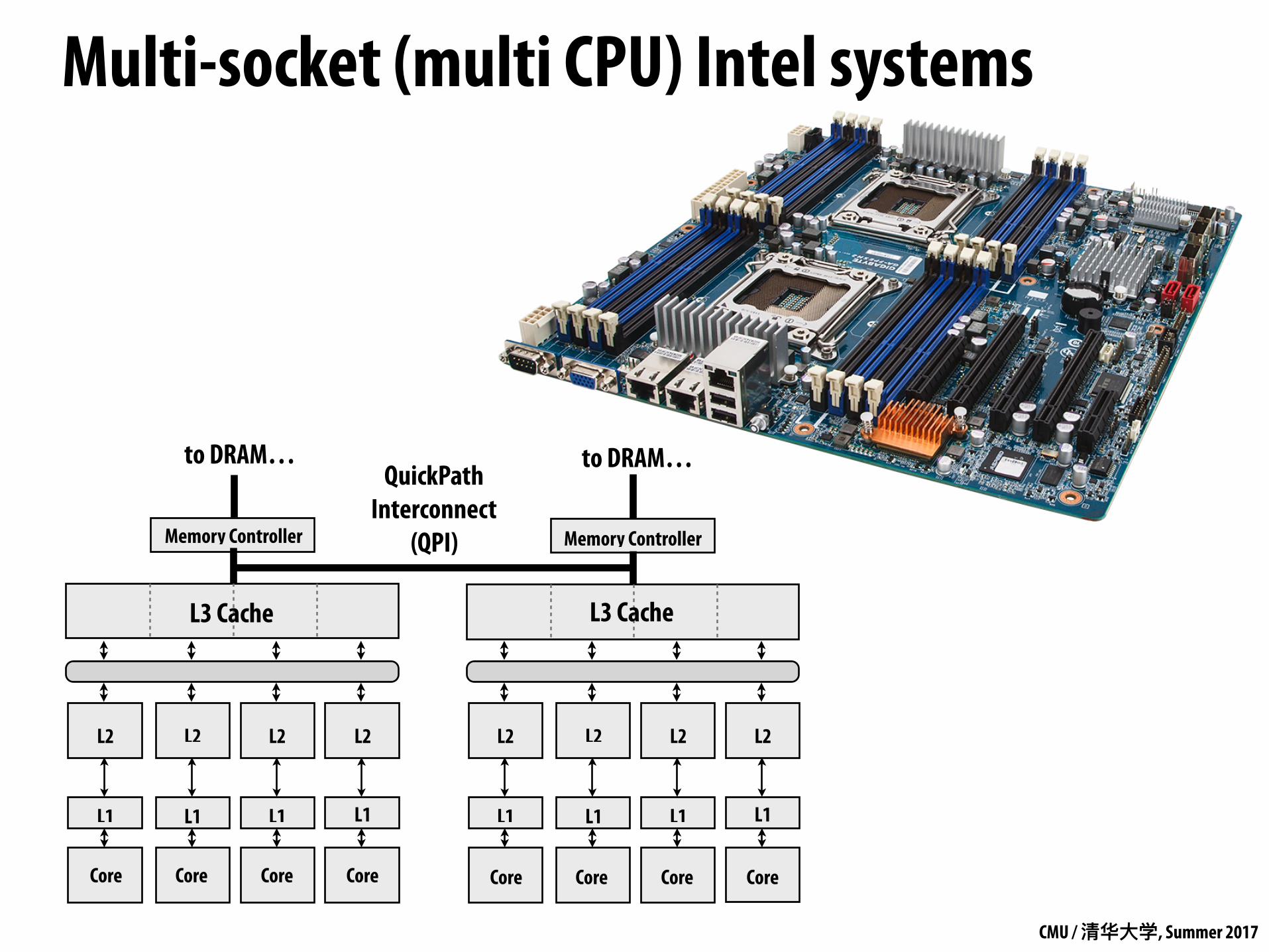
Multi-socket (multi CPU) Intel systems
L1
L2
L3 Cache
L1
L2
L1
L2
L1
L2
Core
L1
L2
L3 Cache
Core
L1
L2
Core
L1
L2
Core
L1
L2
Memory Controller Memory Controller
QuickPath Interconnect
(QPI)
to DRAM… to DRAM…
Core Core Core Core
CMU / 清华⼤大学, Summer 2017
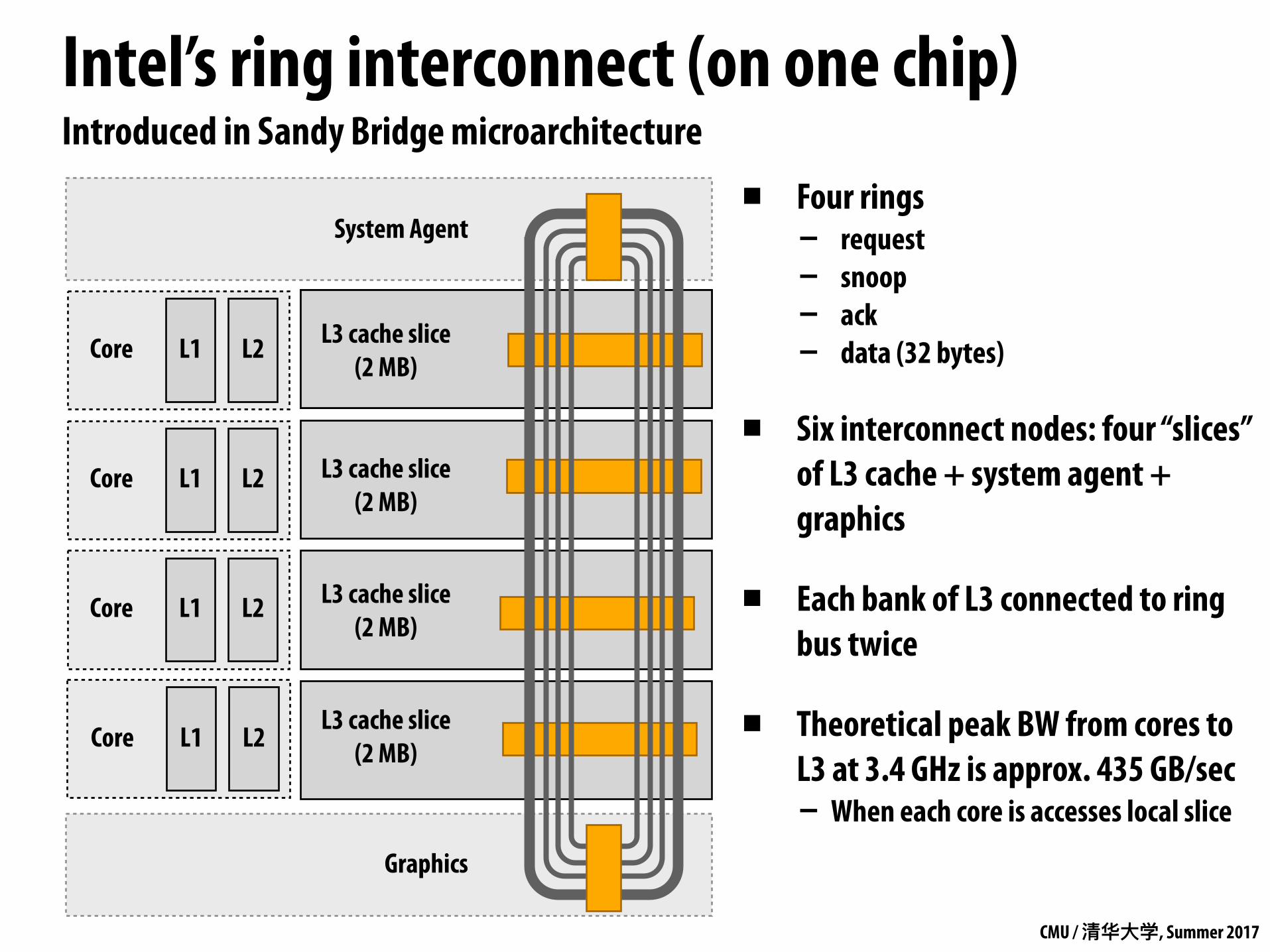
Intel’s ring interconnect (on one chip)Introduced in Sandy Bridge microarchitecture
L3 cache slice (2 MB)
L3 cache slice (2 MB)
L3 cache slice (2 MB)
L3 cache slice (2 MB)
System Agent
Graphics
▪ Four rings - request - snoop - ack - data (32 bytes)
▪ Six interconnect nodes: four “slices” of L3 cache + system agent + graphics
▪ Each bank of L3 connected to ring bus twice
▪ Theoretical peak BW from cores to L3 at 3.4 GHz is approx. 435 GB/sec - When each core is accesses local slice
Core L2L1
Core L2L1
Core L2L1
Core L2L1
CMU / 清华⼤大学, Summer 2017
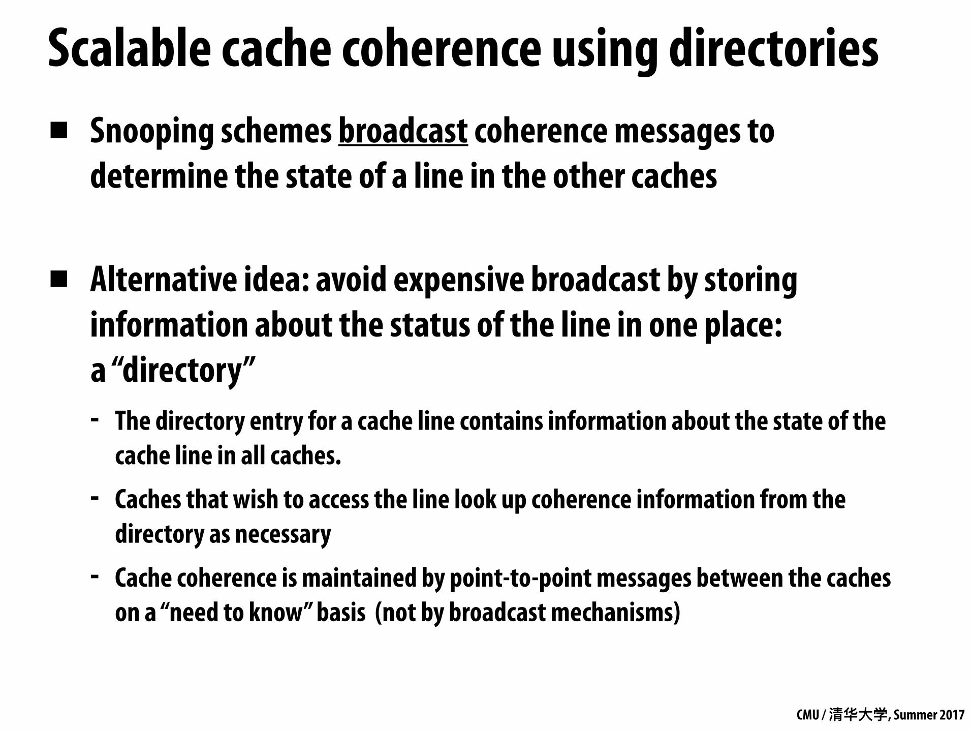
Scalable cache coherence using directories▪ Snooping schemes broadcast coherence messages to
determine the state of a line in the other caches
▪ Alternative idea: avoid expensive broadcast by storing information about the status of the line in one place: a “directory” - The directory entry for a cache line contains information about the state of the
cache line in all caches.
- Caches that wish to access the line look up coherence information from the directory as necessary
- Cache coherence is maintained by point-to-point messages between the caches on a “need to know” basis (not by broadcast mechanisms)
CMU / 清华⼤大学, Summer 2017
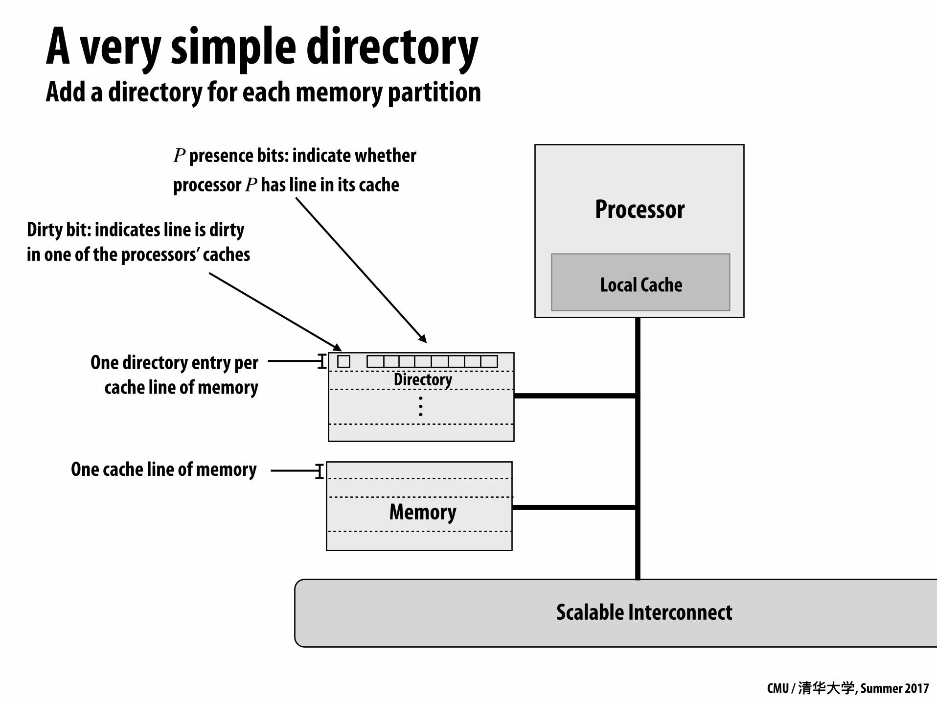
A very simple directoryAdd a directory for each memory partition
Scalable Interconnect
Processor
Local Cache
Directory
Memory
. . .
One cache line of memory
One directory entry per cache line of memory
P presence bits: indicate whether processor P has line in its cache
Dirty bit: indicates line is dirty in one of the processors’ caches
CMU / 清华⼤大学, Summer 2017
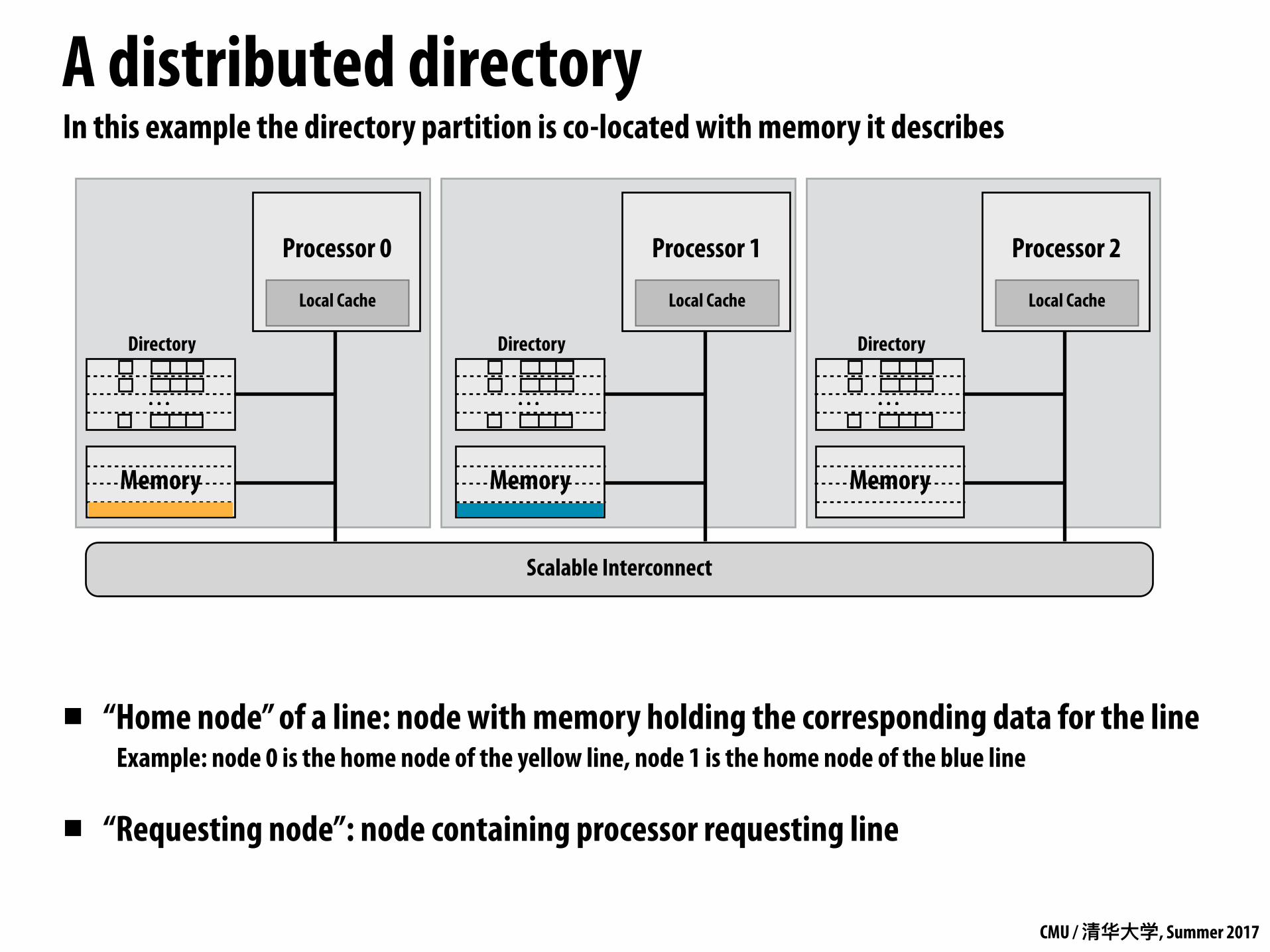
A distributed directory
Scalable Interconnect
Processor 0
Local Cache
Memory
Directory
. . .
Processor 1
Local Cache
Memory
Directory
. . .
Processor 2
Local Cache
Memory
Directory
. . .
▪ “Home node” of a line: node with memory holding the corresponding data for the line Example: node 0 is the home node of the yellow line, node 1 is the home node of the blue line
▪ “Requesting node”: node containing processor requesting line
In this example the directory partition is co-located with memory it describes

CMU / 清华⼤大学, Summer 2017
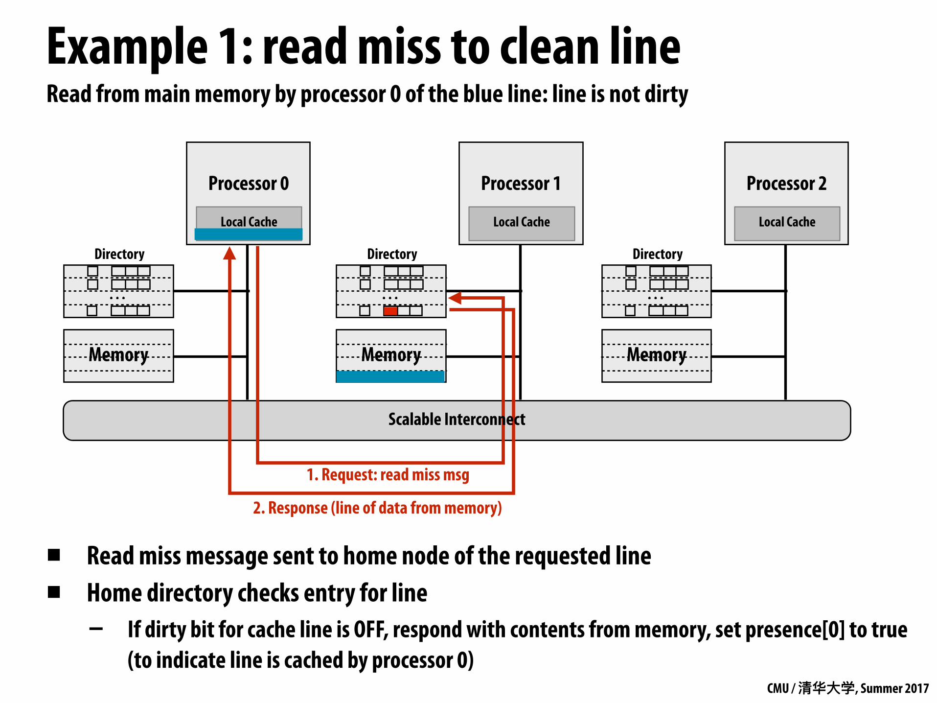
Example 1: read miss to clean line
Processor 0
Local Cache
Memory
Directory
. . .
Processor 1
Local Cache
Memory
Directory
. . .
Processor 2
Local Cache
Memory
Directory
. . .
Read from main memory by processor 0 of the blue line: line is not dirty
▪ Read miss message sent to home node of the requested line
▪ Home directory checks entry for line
1. Request: read miss msg
Scalable Interconnect
CMU / 清华⼤大学, Summer 2017
Example 1: read miss to clean line
Processor 0
Local Cache
Memory
Directory
. . .
Processor 1
Local Cache
Memory
Directory
. . .
Processor 2
Local Cache
Memory
Directory
. . .
Read from main memory by processor 0 of the blue line: line is not dirty
▪ Read miss message sent to home node of the requested line ▪ Home directory checks entry for line - If dirty bit for cache line is OFF, respond with contents from memory, set presence[0] to true
(to indicate line is cached by processor 0)
2. Response (line of data from memory)
1. Request: read miss msg
Scalable Interconnect
CMU / 清华⼤大学, Summer 2017
Example 2: read miss to dirty line
Processor 0
Local Cache
Memory
Directory
. . .
Processor 1
Local Cache
Memory
Directory
. . .
Processor 2
Local Cache
Memory
Directory
. . .
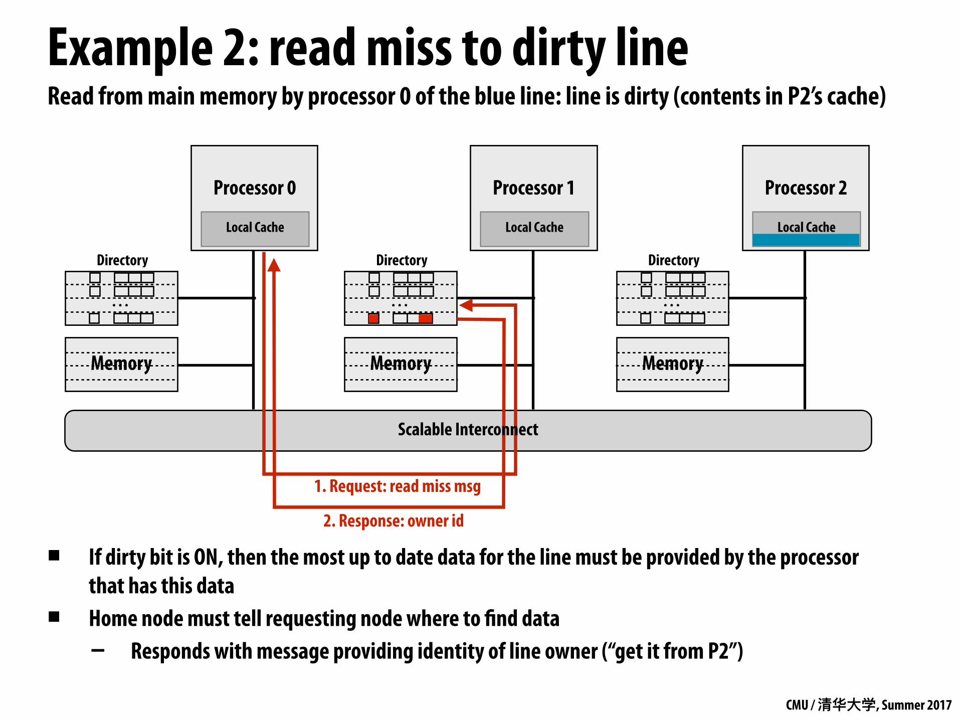
Read from main memory by processor 0 of the blue line: line is dirty (contents in P2’s cache)
▪ If dirty bit is ON, then the most up to date data for the line must be provided by the processor that has this data
▪ Home node must tell requesting node where to find data - Responds with message providing identity of line owner (“get it from P2”)
2. Response: owner id
1. Request: read miss msg
Scalable Interconnect
CMU / 清华⼤大学, Summer 2017
Example 2: read miss to dirty line
Processor 0
Local Cache
Memory
Directory
. . .
Processor 1
Local Cache
Memory
Directory
. . .
Processor 2
Local Cache
Memory
Directory
. . .
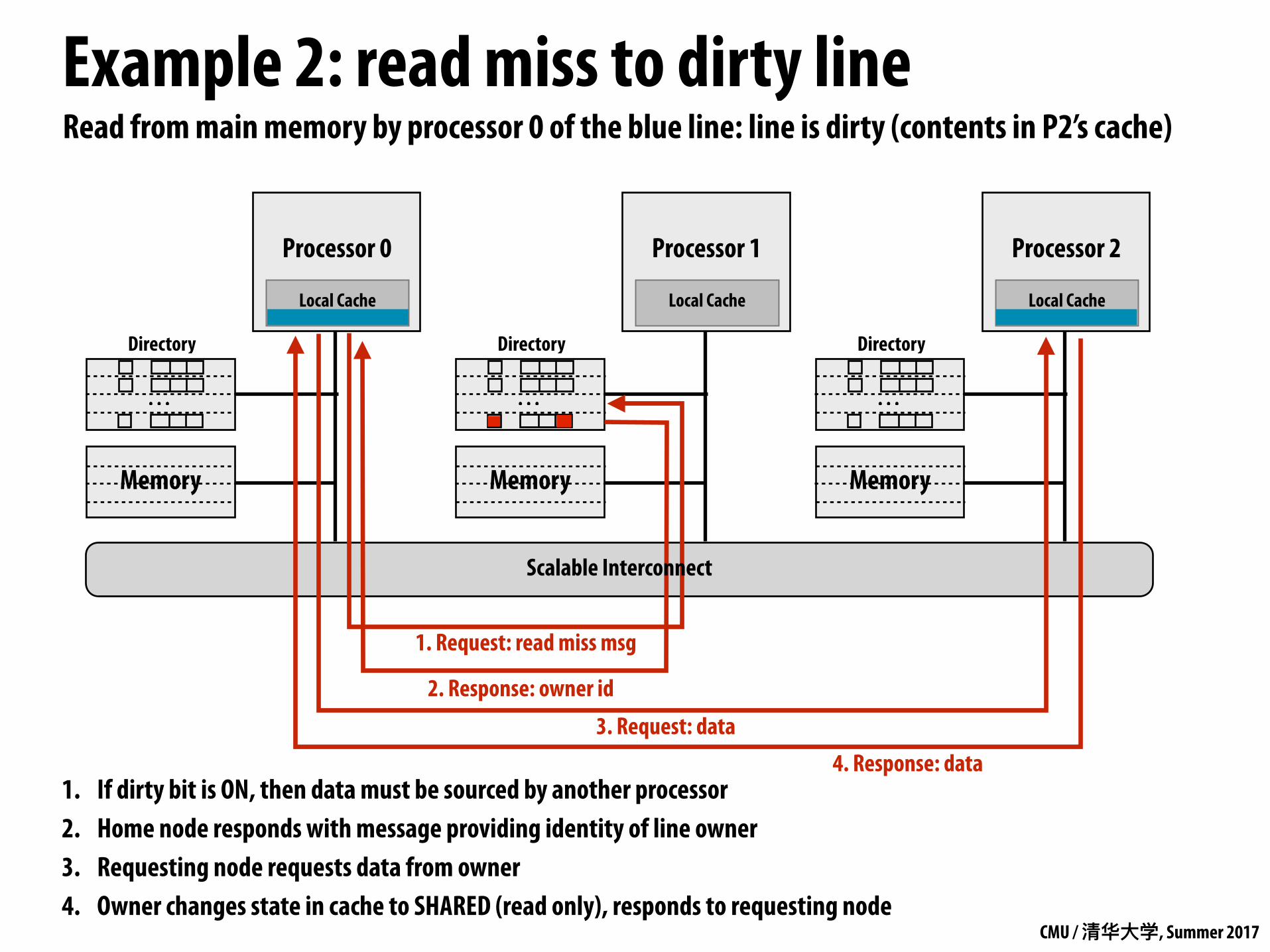
Read from main memory by processor 0 of the blue line: line is dirty (contents in P2’s cache)
1. If dirty bit is ON, then data must be sourced by another processor 2. Home node responds with message providing identity of line owner 3. Requesting node requests data from owner 4. Owner changes state in cache to SHARED (read only), responds to requesting node
2. Response: owner id
1. Request: read miss msg
3. Request: data4. Response: data
Scalable Interconnect
CMU / 清华⼤大学, Summer 2017
Example 2: read miss to dirty line
Processor 0
Local Cache
Memory
Directory
. . .
Processor 1
Local Cache
Memory
Directory
. . .
Processor 2
Local Cache
Memory
Directory
. . .
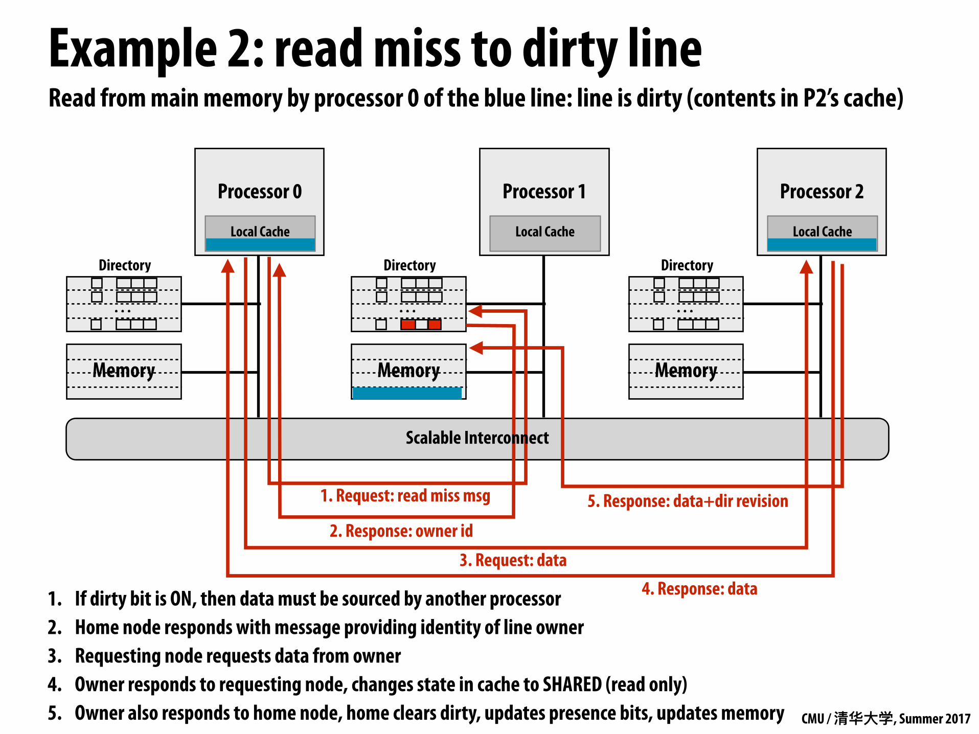
Read from main memory by processor 0 of the blue line: line is dirty (contents in P2’s cache)
1. If dirty bit is ON, then data must be sourced by another processor 2. Home node responds with message providing identity of line owner 3. Requesting node requests data from owner 4. Owner responds to requesting node, changes state in cache to SHARED (read only) 5. Owner also responds to home node, home clears dirty, updates presence bits, updates memory
2. Response: owner id
1. Request: read miss msg
3. Request: data4. Response: data
5. Response: data+dir revision
Scalable Interconnect
CMU / 清华⼤大学, Summer 2017
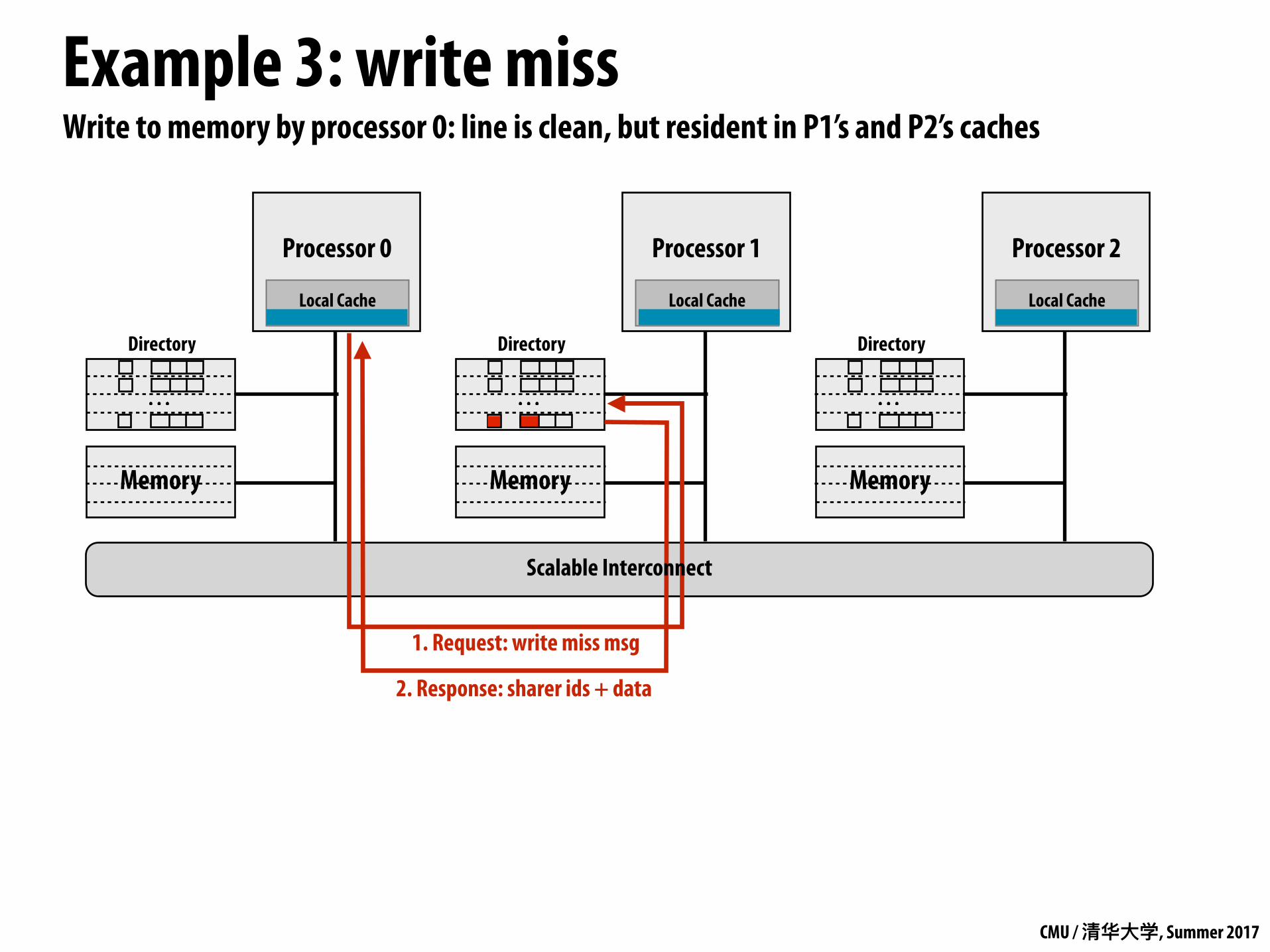
Example 3: write miss
Processor 0
Local Cache
Memory
Directory
. . .
Processor 1
Local Cache
Memory
Directory
. . .
Processor 2
Local Cache
Memory
Directory
. . .
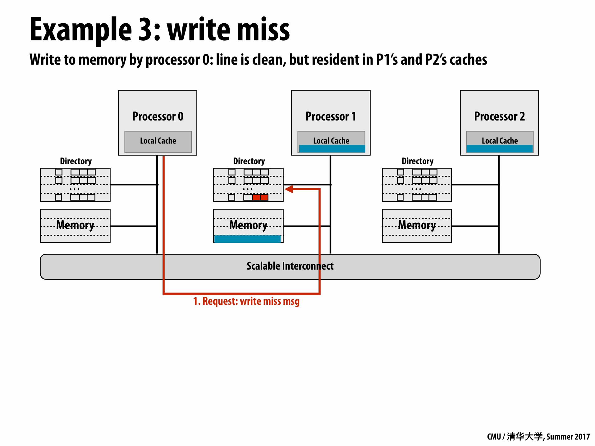
Write to memory by processor 0: line is clean, but resident in P1’s and P2’s caches
1. Request: write miss msg
Scalable Interconnect
CMU / 清华⼤大学, Summer 2017
Example 3: write miss
Processor 0
Local Cache
Memory
Directory
. . .
Processor 1
Local Cache
Memory
Directory
. . .
Processor 2
Local Cache
Memory
Directory
. . .
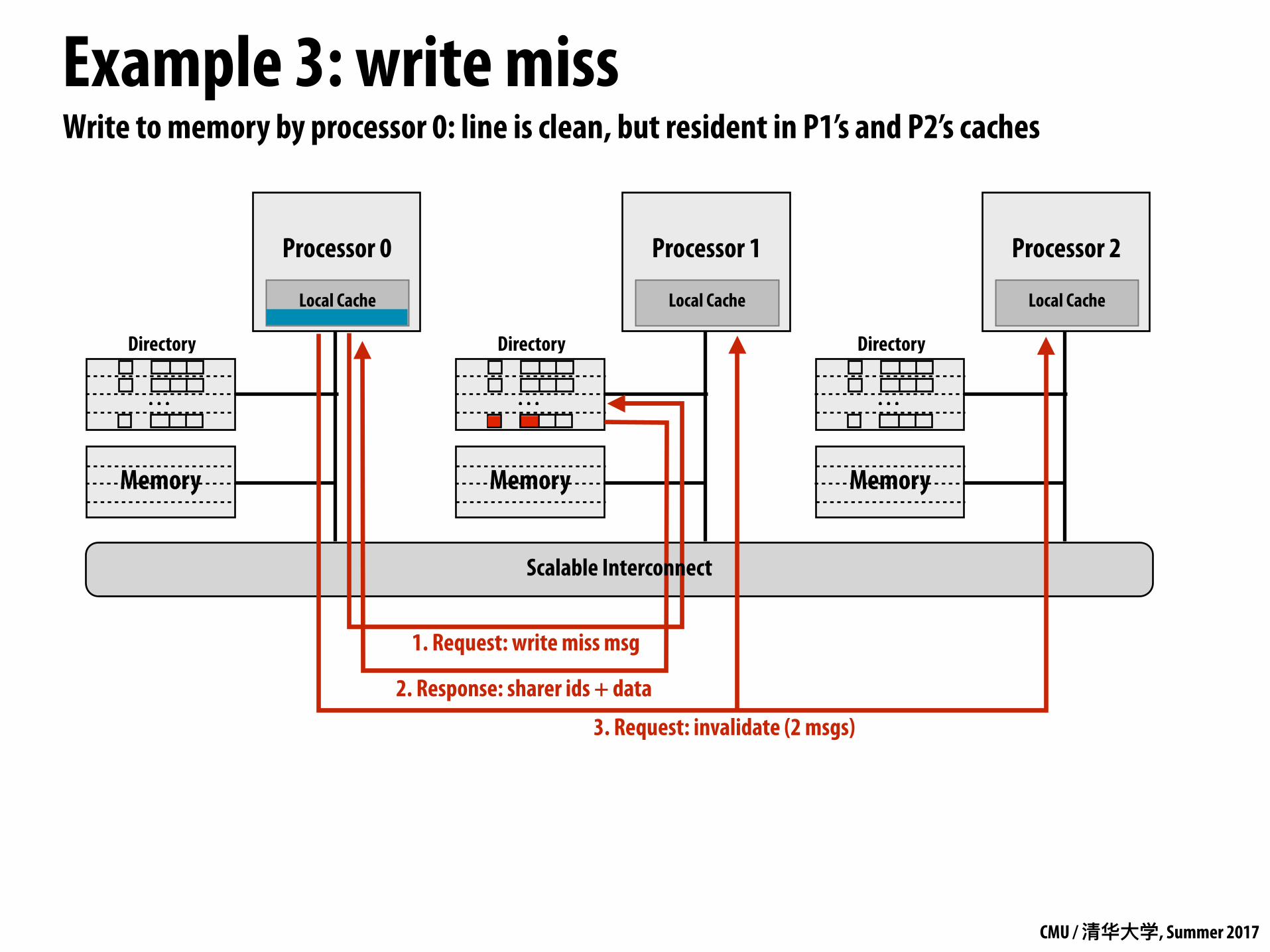
Write to memory by processor 0: line is clean, but resident in P1’s and P2’s caches
1. Request: write miss msg
2. Response: sharer ids + data
Scalable Interconnect
CMU / 清华⼤大学, Summer 2017
Example 3: write miss
Processor 0
Local Cache
Memory
Directory
. . .
Processor 1
Local Cache
Memory
Directory
. . .
Processor 2
Local Cache
Memory
Directory
. . .
Write to memory by processor 0: line is clean, but resident in P1’s and P2’s caches
1. Request: write miss msg
3. Request: invalidate (2 msgs)
2. Response: sharer ids + data
Scalable Interconnect
CMU / 清华⼤大学, Summer 2017
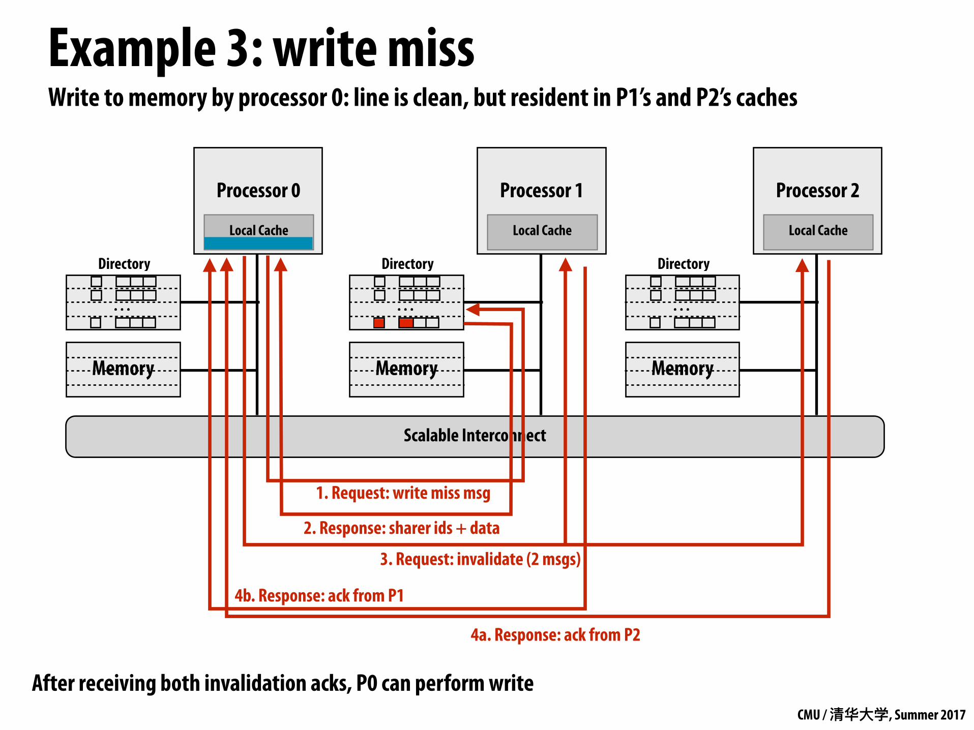
Example 3: write miss
Scalable Interconnect
Processor 0
Local Cache
Memory
Directory
. . .
Processor 1
Local Cache
Memory
Directory
. . .
Processor 2
Local Cache
Memory
Directory
. . .
Write to memory by processor 0: line is clean, but resident in P1’s and P2’s caches
1. Request: write miss msg
3. Request: invalidate (2 msgs)
2. Response: sharer ids + data
4a. Response: ack from P2
4b. Response: ack from P1
After receiving both invalidation acks, P0 can perform write
CMU / 清华⼤大学, Summer 2017
Advantage of directories▪ On reads, the directory tells requesting node exactly where to
get the line from - Either from home node (if the line is clean) - Or from the owning node (if the line is dirty) - Either way, retrieving data involves only point-to-point communication
▪ On writes, the advantage of directories depends on the number of sharers - In the limit, if all caches are sharing data, all caches must be
communicated with (just like broadcast in a snooping protocol)
CMU / 清华⼤大学, Summer 2017
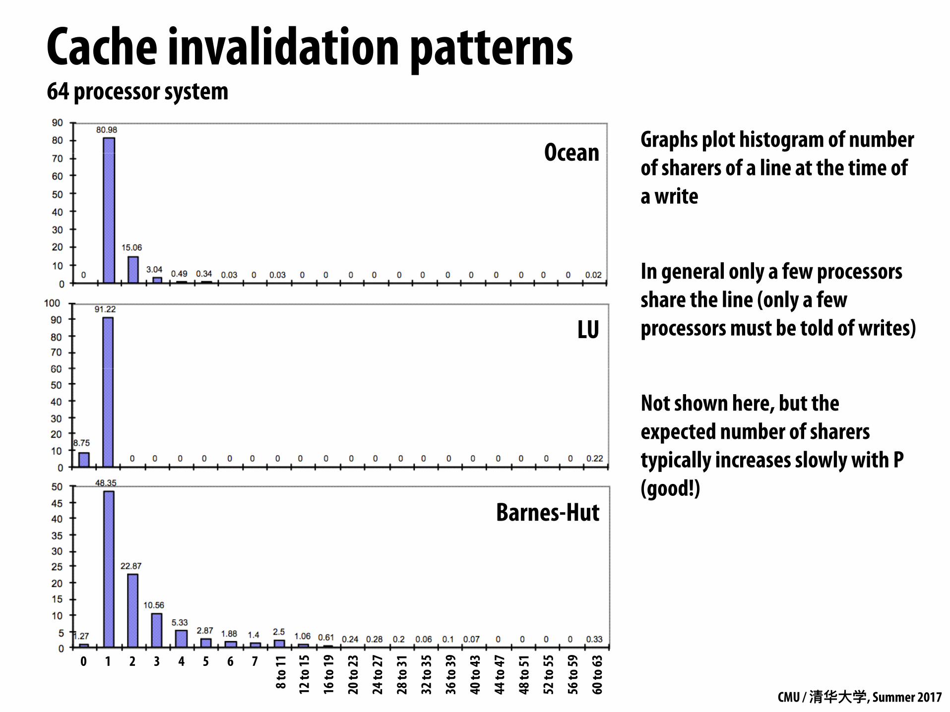
Cache invalidation patterns64 processor system
Barnes-Hut
LU
Ocean
0 1 2 3 4 5 6 7
8 to 1
1
12 to
15
16 to
19
20 to
23
24 to
27
28 to
31
32 to
35
36 to
39
40 to
43
44 to
47
48 to
51
52 to
55
56 to
59
60 to
63
Graphs plot histogram of number of sharers of a line at the time of a write
In general only a few processors share the line (only a few processors must be told of writes)
Not shown here, but the expected number of sharers typically increases slowly with P (good!)
CMU / 清华⼤大学, Summer 2017
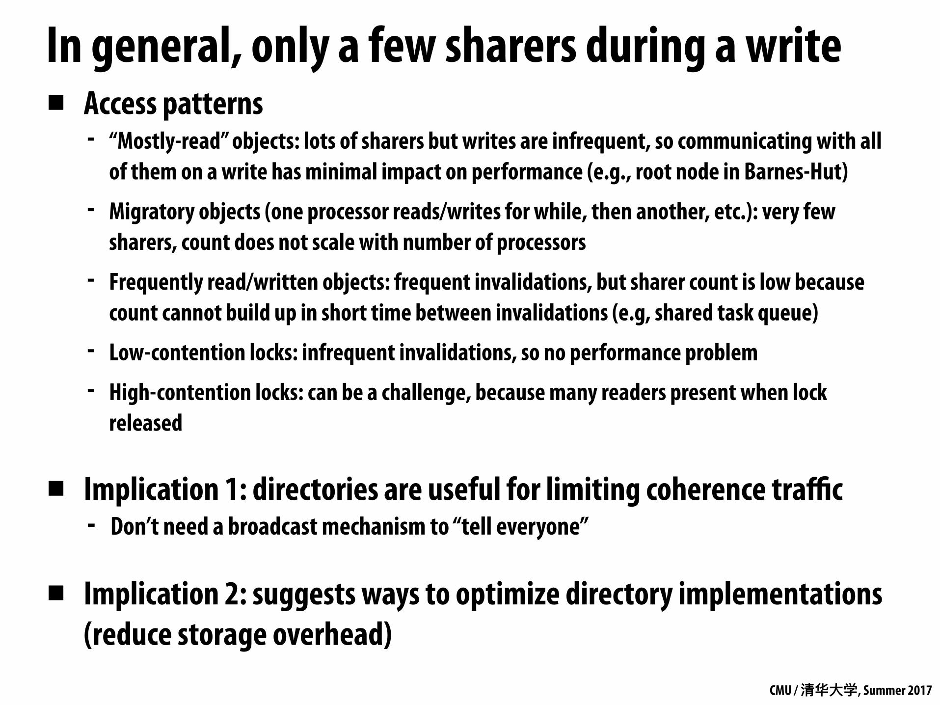
In general, only a few sharers during a write ▪ Access patterns
- “Mostly-read” objects: lots of sharers but writes are infrequent, so communicating with all of them on a write has minimal impact on performance (e.g., root node in Barnes-Hut)
- Migratory objects (one processor reads/writes for while, then another, etc.): very few sharers, count does not scale with number of processors
- Frequently read/written objects: frequent invalidations, but sharer count is low because count cannot build up in short time between invalidations (e.g, shared task queue)
- Low-contention locks: infrequent invalidations, so no performance problem
- High-contention locks: can be a challenge, because many readers present when lock released
▪ Implication 1: directories are useful for limiting coherence traffic - Don’t need a broadcast mechanism to “tell everyone”
▪ Implication 2: suggests ways to optimize directory implementations (reduce storage overhead)
CMU / 清华⼤大学, Summer 2017
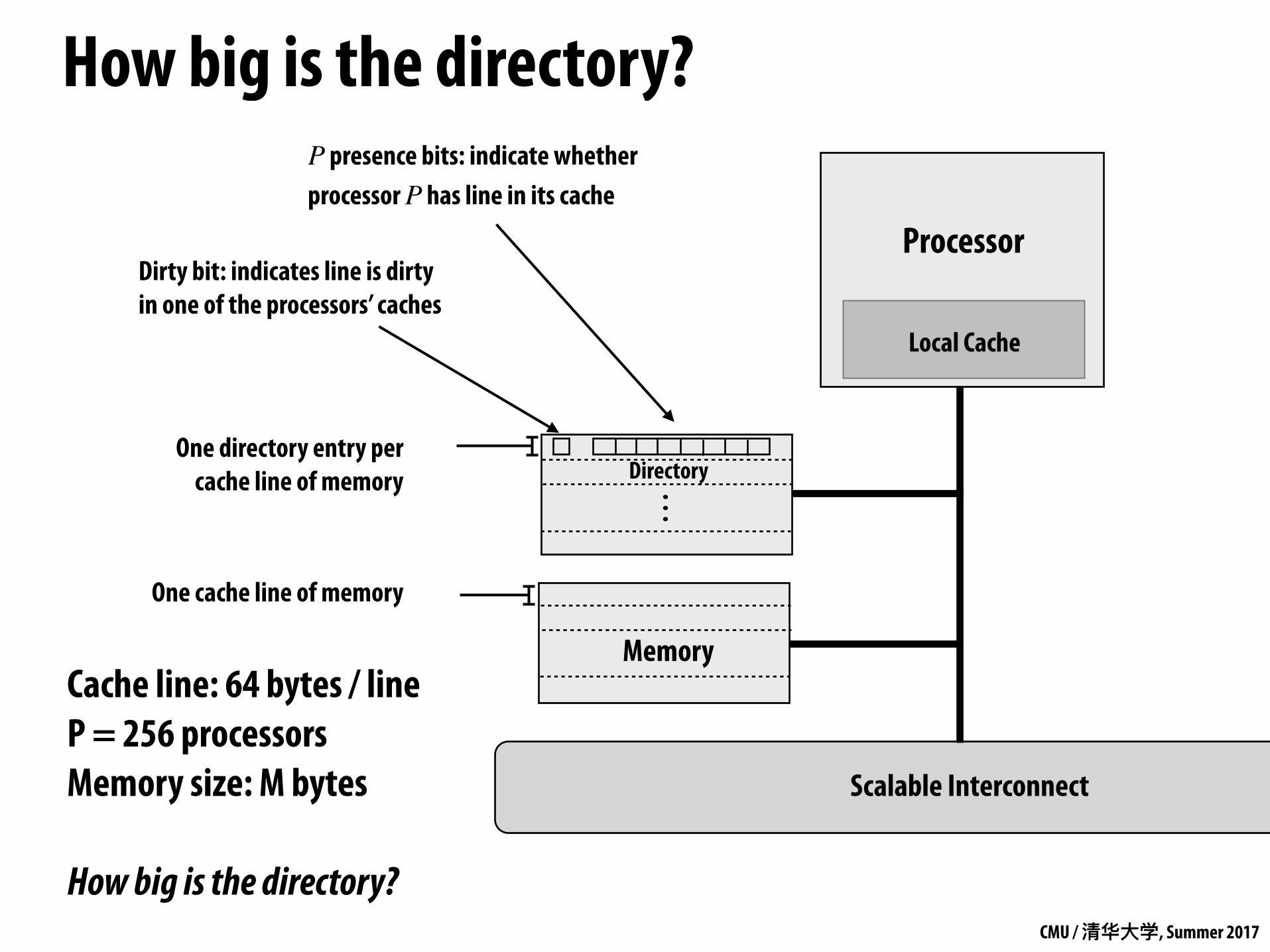
How big is the directory?
Scalable Interconnect
Processor
Local Cache
Directory
Memory. .
.
One cache line of memory
One directory entry per cache line of memory
P presence bits: indicate whether processor P has line in its cache
Dirty bit: indicates line is dirty in one of the processors’ caches
Cache line: 64 bytes / line P = 256 processors Memory size: M bytes
How big is the directory?

CMU / 清华⼤大学, Summer 2017
Full bit vector directory representation▪ Recall: one presence bit per node
▪ Storage proportional to P x M - P = number of nodes (e.g., processors) - M = number of lines in memory
▪ Storage overhead rises with P - Assume 64 byte cache line size (512 bits) - 64 nodes (P=64) →12% overhead - 256 nodes (P=256) → 50% overhead - 1024 nodes (P=1024) → 200% overhead
. . .
P
M
. . .
CMU / 清华⼤大学, Summer 2017
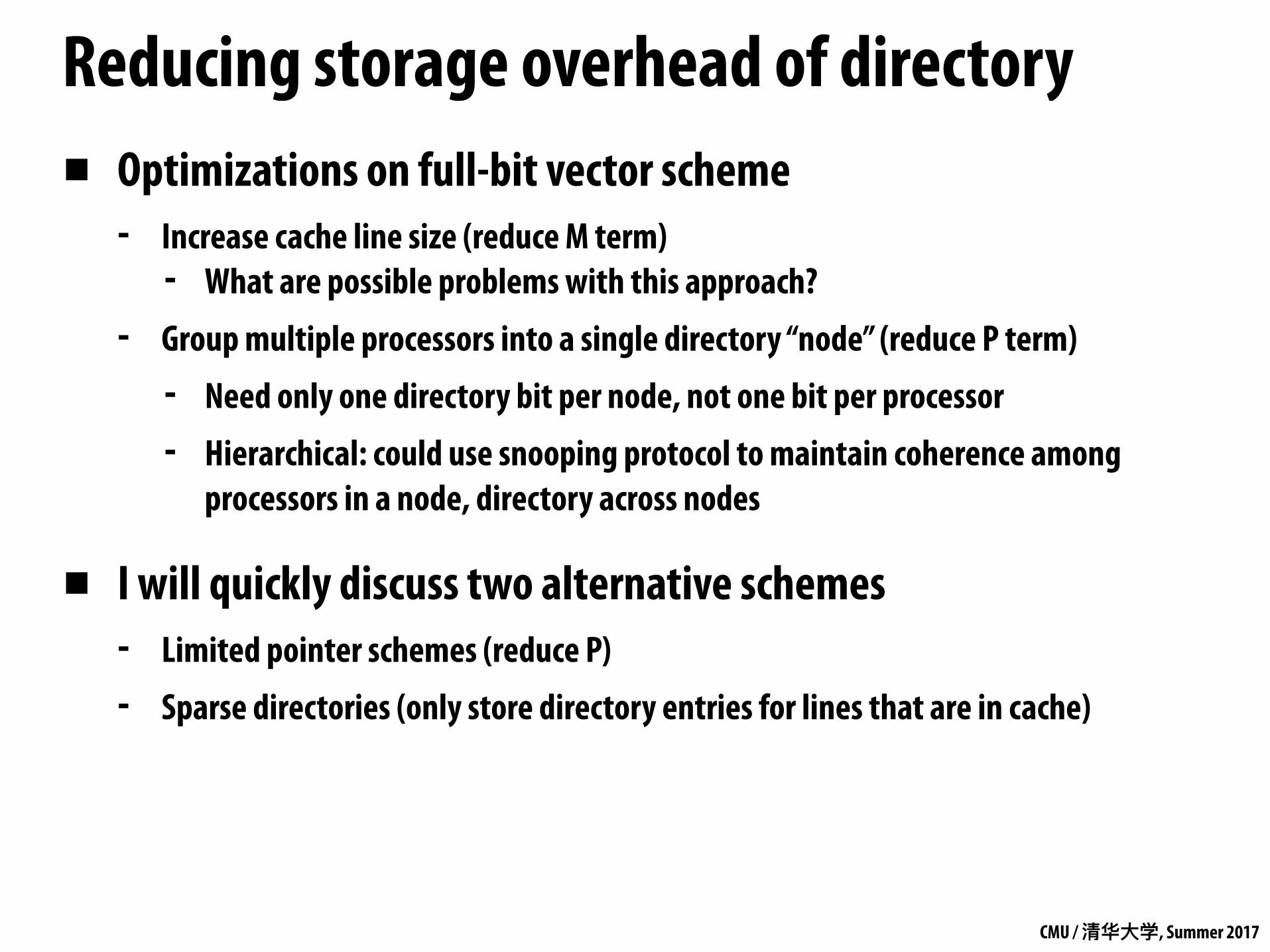
Reducing storage overhead of directory▪ Optimizations on full-bit vector scheme
- Increase cache line size (reduce M term) - What are possible problems with this approach?
- Group multiple processors into a single directory “node” (reduce P term)
- Need only one directory bit per node, not one bit per processor
- Hierarchical: could use snooping protocol to maintain coherence among processors in a node, directory across nodes
▪ I will quickly discuss two alternative schemes - Limited pointer schemes (reduce P)
- Sparse directories (only store directory entries for lines that are in cache)
CMU / 清华⼤大学, Summer 2017
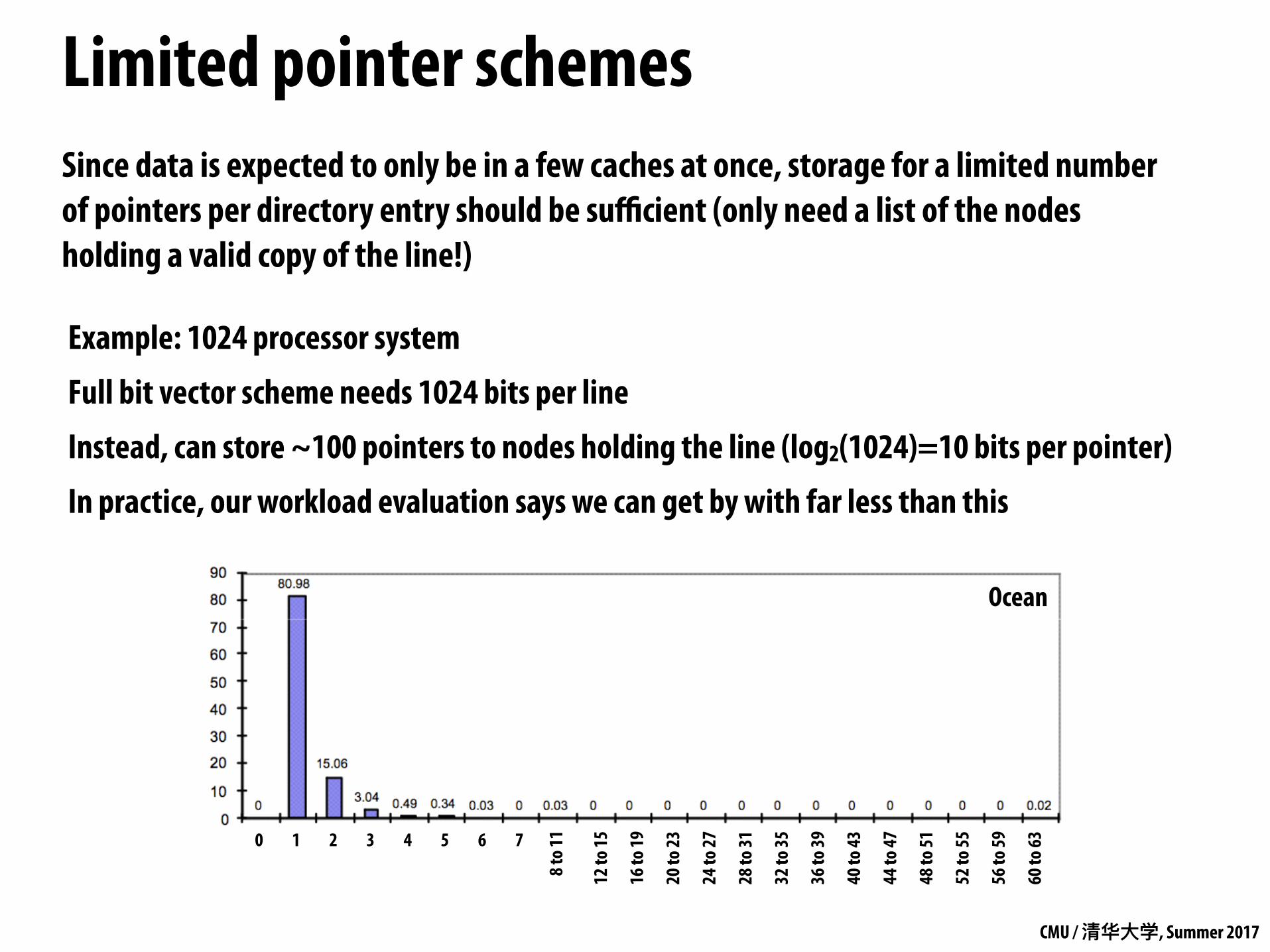
Limited pointer schemesSince data is expected to only be in a few caches at once, storage for a limited number of pointers per directory entry should be sufficient (only need a list of the nodes holding a valid copy of the line!)
Ocean
Example: 1024 processor system
Full bit vector scheme needs 1024 bits per line
Instead, can store ~100 pointers to nodes holding the line (log2(1024)=10 bits per pointer)
In practice, our workload evaluation says we can get by with far less than this
0 1 2 3 4 5 6 7
8 to 1
1
12 to
15
16 to
19
20 to
23
24 to
27
28 to
31
32 to
35
36 to
39
40 to
43
44 to
47
48 to
51
52 to
55
56 to
59
60 to
63

CMU / 清华⼤大学, Summer 2017
Managing overflow in limited pointer schemes
▪ Fallback to broadcast (if broadcast mechanism exists) - When more than max number of sharers, revert to broadcast
▪ If no broadcast mechanism present on machine - Do not allow more than a max number of sharers - On overflow, newest sharer replaces an existing one
(must invalidate line in the old sharer’s cache)
▪ Coarse vector fallback - Revert to bit vector representation representation - Each bit corresponds to K nodes - On write, invalidate all nodes a bit corresponds to
Many possible approaches

CMU / 清华⼤大学, Summer 2017
Optimizing for the common case
Limited pointer schemes are a great example of smartly understanding and optimizing for the common case:
1. Workload-driven observation: in general the number of cache line sharers is low
2. Make the common case simple and fast: array of pointers for first N sharers
3. Uncommon case is still handled correctly, just with a slower, more complicated mechanism (the program still works!)
4. Extra expense of the complicated solution is tolerable, since it happens infrequently
CMU / 清华⼤大学, Summer 2017
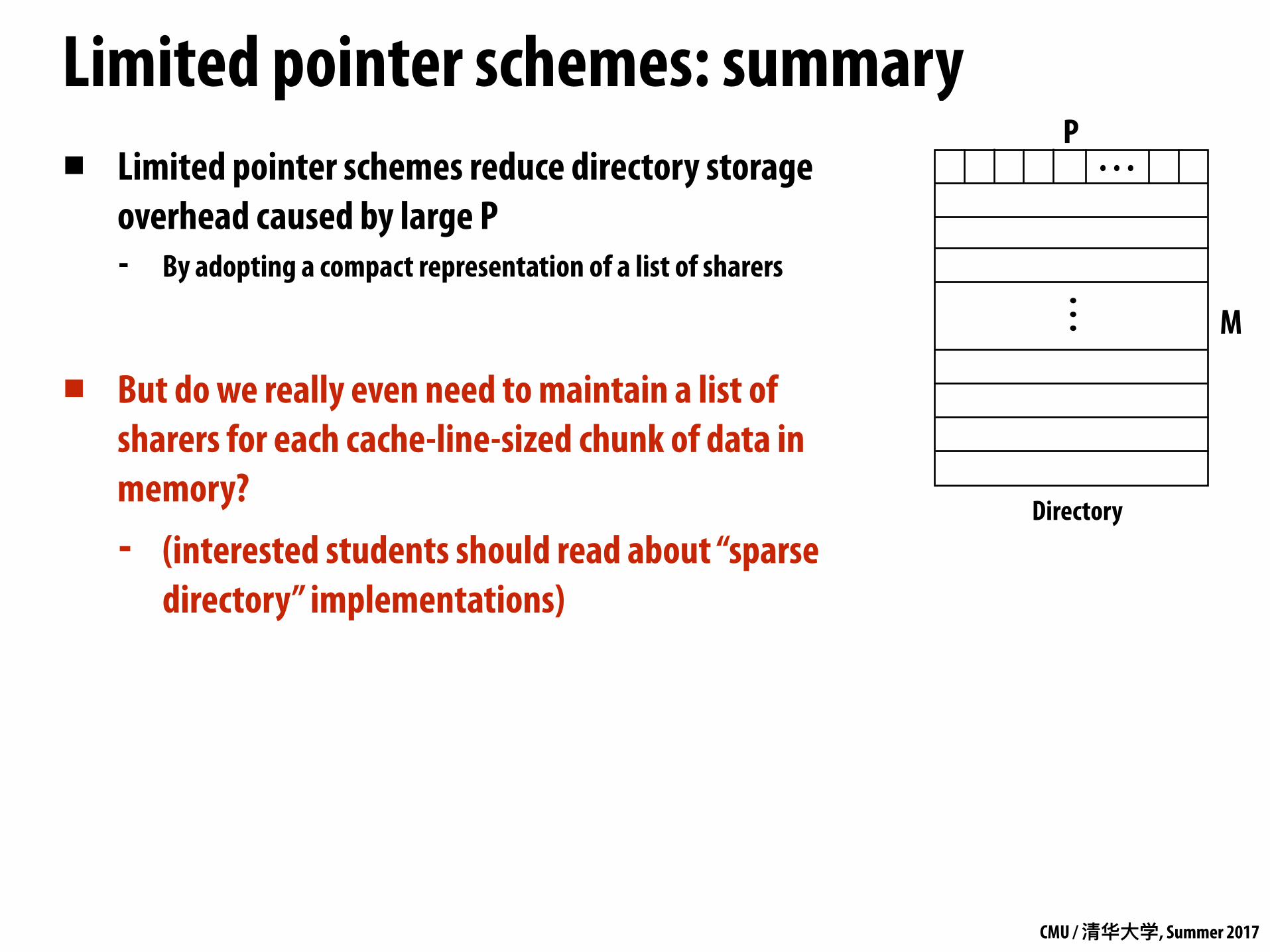
Limited pointer schemes: summary▪ Limited pointer schemes reduce directory storage
overhead caused by large P - By adopting a compact representation of a list of sharers
▪ But do we really even need to maintain a list of sharers for each cache-line-sized chunk of data in memory?
- (interested students should read about “sparse directory” implementations)
. . .
P
M
. . .
Directory

CMU / 清华⼤大学, Summer 2017
Directory coherence in Intel Core i7 CPU▪ L3 stores a directory for all lines
in the L3 cache (note importance of inclusion property… there will be a directory entry for any line in an L2)
▪ Directory maintains list of L2 caches containing line
▪ Instead of broadcasting coherence traffic to all L2’s, only send coherence messages to L2’s that contain the line (Core i7 interconnect is a ring, it is not a bus)
▪ Directory dimensions: - P=4 - M = number of L3 cache lines
Core
L1 Data Cache
L2 Cache
Shared L3 Cache (One bank per core)
Ring Interconnect
Core
L1 Data Cache
L2 Cache
Core
L1 Data Cache
L2 Cache
Core
L1 Data Cache
L2 Cache

CMU / 清华⼤大学, Summer 2017
Coherence in multi-socket Intel systems
Core
L1
L2
L3 Cache
Core
L1
L2
Core
L1
L2
Core
L1
L2
Core
L1
L2
L3 Cache
Core
L1
L2
Core
L1
L2
Core
L1
L2
Cache Agent Cache Agent
Memory Controller Memory Controller
Home Agent Home AgentQuickPath Interconnect
(QPI)
to DRAM… (with in memory directory)
Dir cache (16KB) Dir cache (16KB)
to DRAM… (in memory directory) ▪ L3 directory reduces on-chip
coherence traffic (previous slide)
▪ In-memory directory (cached by home agent/memory controller) reduces coherence traffic between cores
CMU / 清华⼤大学, Summer 2017
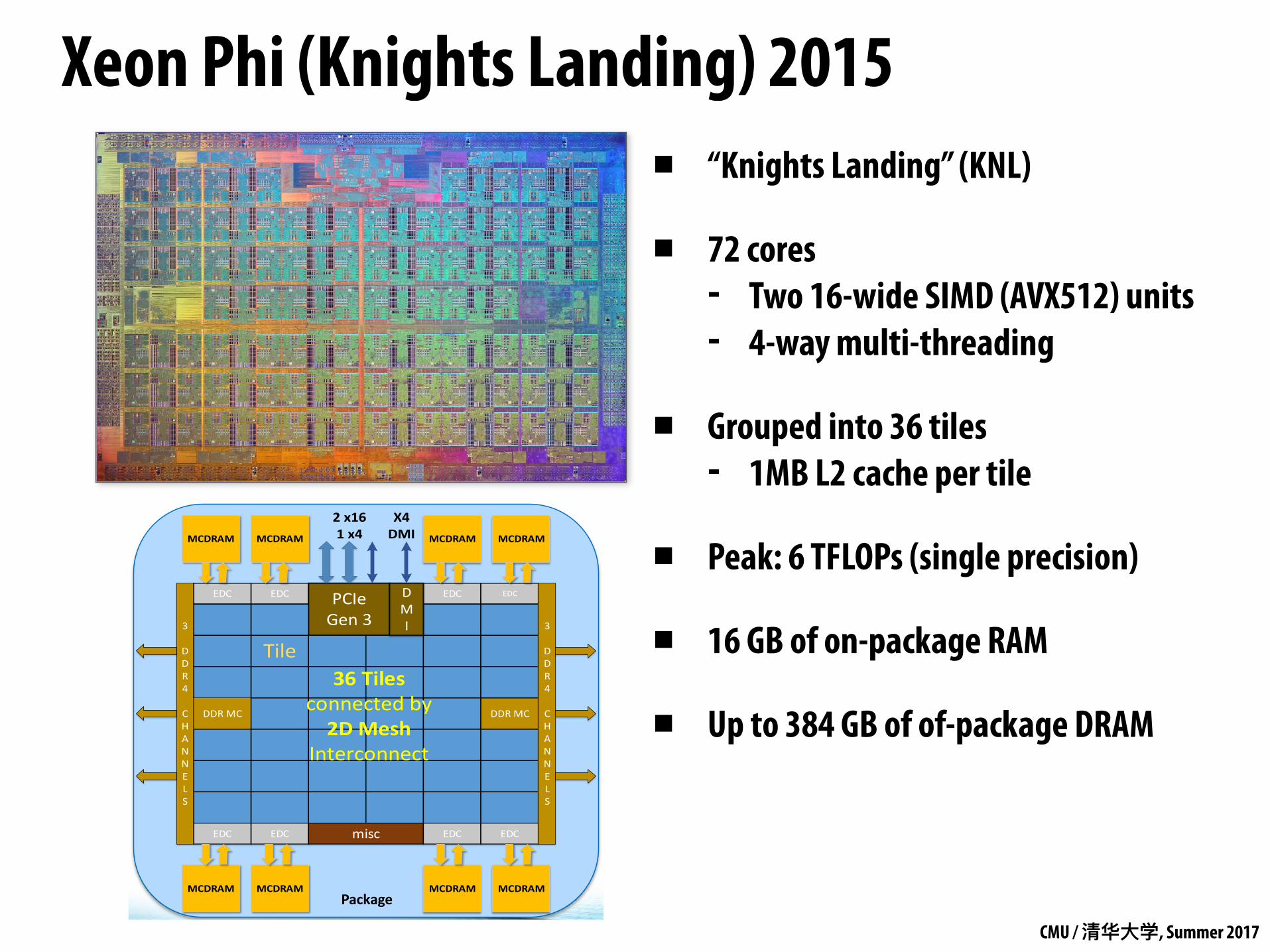
Xeon Phi (Knights Landing) 2015▪ “Knights Landing” (KNL)
▪ 72 cores - Two 16-wide SIMD (AVX512) units - 4-way multi-threading
▪ Grouped into 36 tiles - 1MB L2 cache per tile
▪ Peak: 6 TFLOPs (single precision)
▪ 16 GB of on-package RAM
▪ Up to 384 GB of of-package DRAM
Knights Landing Overview
Chip: 36 Tiles interconnected by 2D Mesh Tile: 2 Cores + 2 VPU/core + 1 MB L2 Memory: MCDRAM: 16 GB on-package; High BW DDR4: 6 channels @ 2400 up to 384GB IO: 36 lanes PCIe Gen3. 4 lanes of DMI for chipset Node: 1-Socket only Fabric: Omni-Path on-package (not shown) Vector Peak Perf: 3+TF DP and 6+TF SP Flops Scalar Perf: ~3x over Knights Corner Streams Triad (GB/s): MCDRAM : 400+; DDR: 90+
TILE
4
2 VPU
Core
2 VPU
Core
1MB L2
CHA
Package
Source Intel: All products, computer systems, dates and figures specified are preliminary based on current expectations, and are subject to change without notice. KNL data are preliminary based on current expectations and are subject to change without notice. 1Binary Compatible with Intel Xeon processors using Haswell Instruction Set (except TSX). 2Bandwidth numbers are based on STREAM-like memory access pattern when MCDRAM used as flat memory. Results have been estimated based on internal Intel analysis and are provided for informational purposes only. Any difference in system hardware or software design or configuration may affect actual performance. Omni-path not shown
EDC EDC PCIe Gen 3
EDC EDC
Tile
DDR MC DDR MC
EDC EDC misc EDC EDC
36 Tiles connected by
2D Mesh Interconnect
MCDRAM MCDRAM MCDRAM MCDRAM
3
DDR4
CHANNELS
3
DDR4
CHANNELS
MCDRAM MCDRAM MCDRAM MCDRAM
DMI
2 x161 x4
X4 DMI
CMU / 清华⼤大学, Summer 2017
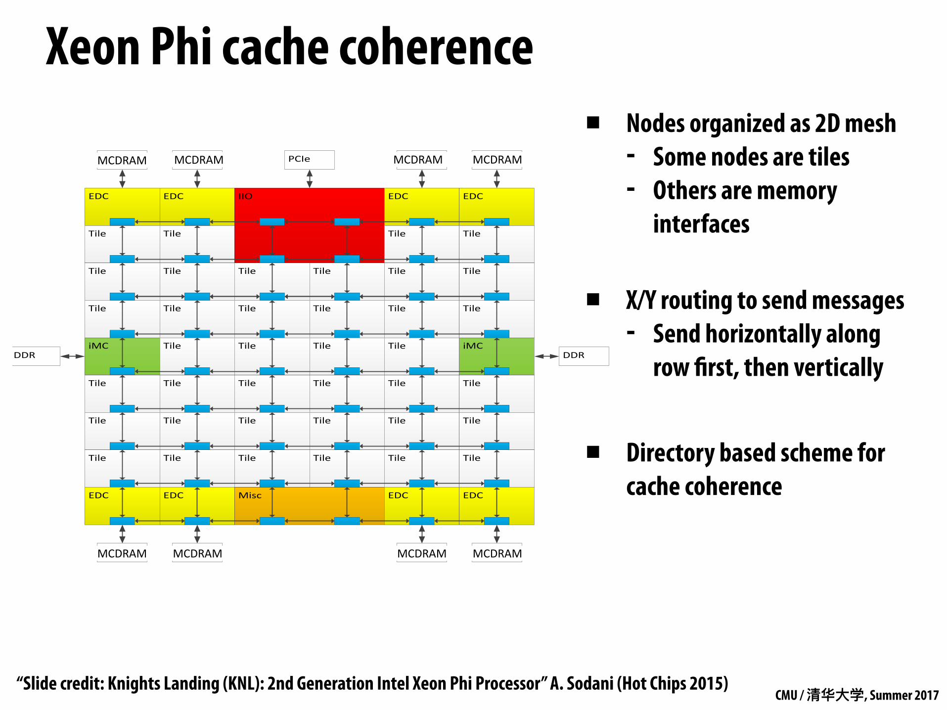
Xeon Phi cache coherenceKNL Mesh Interconnect
Mesh of Rings � Every row and column is a (half) ring
� YX routing: Go in Y Æ Turn Æ Go in X
� Messages arbitrate at injection and on turn
Cache Coherent Interconnect � MESIF protocol (F = Forward)
� Distributed directory to filter snoops
Three Cluster Modes (1) All-to-All (2) Quadrant (3) Sub-NUMA Clustering
Misc
IIOEDC EDC
Tile Tile
Tile Tile Tile
EDC EDC
Tile Tile
Tile Tile Tile
Tile Tile Tile Tile Tile Tile
Tile Tile Tile Tile Tile Tile
Tile Tile Tile Tile Tile Tile
Tile Tile Tile Tile Tile Tile
EDC EDC EDC EDC
iMC Tile Tile Tile Tile iMC
OPIO OPIO OPIO OPIO
OPIO OPIO OPIO OPIO
PCIe
DDR DDR
MCDRAM MCDRAM MCDRAM MCDRAM
MCDRAM MCDRAM MCDRAM MCDRAM
▪ Nodes organized as 2D mesh - Some nodes are tiles - Others are memory
interfaces
▪ X/Y routing to send messages - Send horizontally along
row first, then vertically
▪ Directory based scheme for cache coherence
“Slide credit: Knights Landing (KNL): 2nd Generation Intel Xeon Phi Processor” A. Sodani (Hot Chips 2015)
CMU / 清华⼤大学, Summer 2017
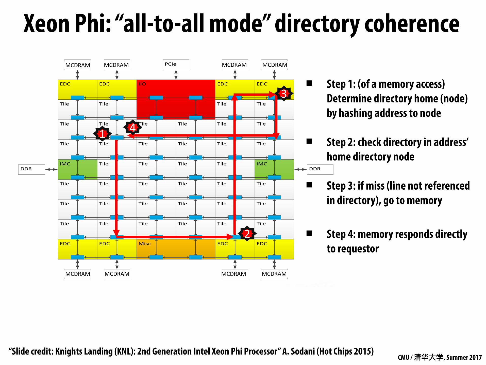
Xeon Phi: “all-to-all mode” directory coherenceCluster Mode: All-to-All Address uniformly hashed across all distributed directories
No affinity between Tile, Directory and Memory
Most general mode. Lower performance than other modes.
Typical Read L2 miss 1. L2 miss encountered
2. Send request to the distributed directory
3. Miss in the directory. Forward to memory
4. Memory sends the data to the requestor
14
Misc
IIOEDC EDC
Tile Tile
Tile Tile Tile
EDC EDC
Tile Tile
Tile Tile Tile
Tile Tile Tile Tile Tile Tile
Tile Tile Tile Tile Tile Tile
Tile Tile Tile Tile Tile Tile
Tile Tile Tile Tile Tile Tile
EDC EDC EDC EDC
iMC Tile Tile Tile Tile iMC
OPIO OPIO OPIO OPIO
OPIO OPIO OPIO OPIO
PCIe
DDR DDR
1
2
3
4
MCDRAM MCDRAM MCDRAM MCDRAM
MCDRAM MCDRAM MCDRAM MCDRAM
▪ Step 1: (of a memory access) Determine directory home (node) by hashing address to node
▪ Step 2: check directory in address’ home directory node
▪ Step 3: if miss (line not referenced in directory), go to memory
▪ Step 4: memory responds directly to requestor
“Slide credit: Knights Landing (KNL): 2nd Generation Intel Xeon Phi Processor” A. Sodani (Hot Chips 2015)
CMU / 清华⼤大学, Summer 2017
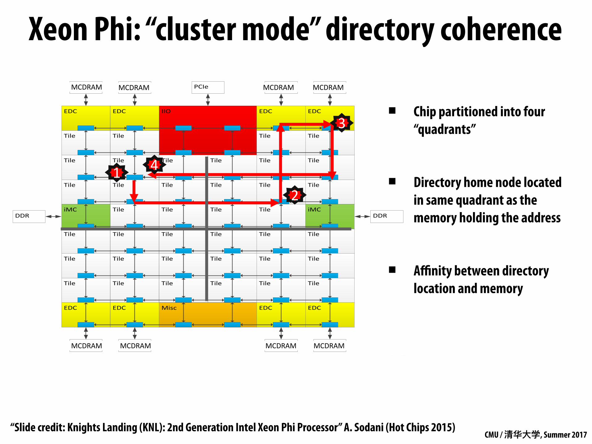
Cluster Mode: Quadrant Chip divided into four virtual Quadrants
Address hashed to a Directory in the same quadrant as the Memory
Affinity between the Directory and Memory
Lower latency and higher BW than all-to-all. SW Transparent.
15
1) L2 miss, 2) Directory access, 3) Memory access, 4) Data return
Misc
IIOEDC EDC
Tile Tile
Tile Tile Tile
EDC EDC
Tile Tile
Tile Tile Tile
Tile Tile Tile Tile Tile Tile
Tile Tile Tile Tile Tile Tile
Tile Tile Tile Tile Tile Tile
Tile Tile Tile Tile Tile Tile
EDC EDC EDC EDC
iMC Tile Tile Tile Tile iMC
OPIO OPIO OPIO OPIO
OPIO OPIO OPIO OPIO
PCIe
DDR DDR
1 2
3
4
MCDRAM MCDRAM MCDRAM MCDRAM
MCDRAM MCDRAM MCDRAM MCDRAM
Xeon Phi: “cluster mode” directory coherence
▪ Chip partitioned into four “quadrants”
▪ Directory home node located in same quadrant as the memory holding the address
▪ Affinity between directory location and memory
“Slide credit: Knights Landing (KNL): 2nd Generation Intel Xeon Phi Processor” A. Sodani (Hot Chips 2015)
CMU / 清华⼤大学, Summer 2017
Summary: directory-based coherence
▪ Primary observation: broadcast does not scale, but luckily we don’t need to broadcast to ensure coherence because often the number of caches containing a copy of a line is small
▪ Instead of snooping, just store the list of sharers in a “directory” and check the list as necessary
▪ One challenge: reducing overhead of directory storage - Use hierarchies of processors or larger line sizes - Limited pointer schemes: exploit fact the most processors not sharing line - Sparse directory schemes: exploit fact that most lines are not in cache