lecture 2 silicon labs c8051f020 system overview
TRANSCRIPT

Lecture 2
Silicon Labs C8051F020
System Overview

2
C8051F020 System Overview
Introduction to CIP-51 C8051F020 system overview Memory organization Program and internal data memories Special function registers I/O ports The digital crossbar 12-Bit analog-to-digital converter 8-Bit analog-to-digital converter Digital-to-analog converter Comparators Voltage reference for ADC and DAC Internal voltage reference generator

3
Introduction to CIP-51
CIP-51 is the CPU of the Silicon Labs C8051F020 MCU
The CIP-51 implements the standard 8051 organization, as well as additional custom peripherals
At 25 MHz, it has a peak throughput of 25 millions of instructions per second (MIPS)
The CIP-51 has a total of 109 instructions

4
C8051F020 System Overview
The Silicon Labs C8051F020 is a fully integrated mixed-signal system-on-a-chip microcontroller available in a 100-pin package Mixed-Signal
Contains both digital and analog peripherals
System-on-a-chip (SOC) Integrates memory, CPU,
peripherals, and clock generator in a single package

5
C8051F020 System Overview—Features
Peak throughput 25 MIPS
FLASH program memory 64 K
On-chip data RAM 4352 bytes
Full-duplex UARTS x 2
16-bit timers x 5
Digital I/O ports 64-pin
12-bit 100 ksps ADC 8 channels
8-bit 500 ksps ADC 8 channels
DAC resolution 12-bit
DAC outputs x 2
Analog comparators x 2
Interrupts 2 levels
PCA (programmable counter arrays) 5 channels
Internal oscillator 25 Mhz
Debug circuitry

6
C8051F020 Functional Block Diagram

7
Memory Organization
The memory organization of C8051F020 is similar to that of a standard 8051
Program and data memory share the same address space but are accessed via different instruction types

8
Program Memory
FLASH memory Can be reprogrammed in-circuit Provides non-volatile data storage Allows field upgrades of the 8051
firmware The C8051F020’s program
memory consists of 65536 bytes of FLASH
512 bytes from addresses 0xFE00 to 0xFFFF are reserved for factory use
128 bytes at address 0x10000 to 0x1007F (scratchpad memory) can be used as non-volatile storage of program constants

9
Internal Data Memory
The internal data memory consists of 256 bytes of RAM
The special function registers (SFR) are accessed when the direct addressing mode is used to access the upper 128 bytes of memory locations from 0x80 to 0xFF
The general purpose RAM are accessed when indirect addressing is used to access the upper 128 bytes
The first 32 bytes of the internal data memory are addressable as four banks of 8 general purpose registers
The next 16 bytes are bit-addressable or byte-addressable

10
Special Function Registers
SFRs provide control and data exchange with the microcontroller’s resources and peripherals
The C8051F020 duplicates the SFRs found in a typical 8051 implementation The C8051F020 implements additional SFRs which are used to
configure and access the sub-systems unique to the microcontroller
This allows the addition of new functionalities while retaining compatibility with the MCS-51 instruction set
The SFRs with addresses ending in 0x0 or 0x8 (e.g. P0, TCON, P1, SCON, IE, etc.) are bit-addressable as well as byte-addressable

11
Special Function Registers
F8 SPI0CN PCA0H PCA0CPH0 PCA0CPH1 PCA0CPH2 PCA0CPH3 PCA0CPH4 WDTCN
F0 B SCON1 SBUF1 SADDR1 TL4 TH4 EIP1 EIP2
E8 ADC0CN PCA0L PCA0CPL0 PCA0CPL1 PCA0CPL2 PCA0CPL3 PCA0CPL4 RSTSRC
E0 ACC XBR0 XBR1 XBR2 RCAP4L RCAP4H EIE1 EIE2
D8 PCA0CN PCA0MD PCA0M0 PCA0CPM1 PCA0CPM2PCA0CPM
3PCA0CPM4
D0 PSW REF0CN DAC0L DAC0H DAC0CN DAC1L DAC1H DAC1CN
C8 T2CON T4CON RCAP2L RCAP2H TL2 TH2 SMB0CR
C0SMB0CN
SMB0STA
SMB0DAT SMB0ADR ADC0GTL ADC0GTH ADC0LTL ADC0LTH
B8 IP SADEN0 AMX0CF AMX0SL ADC0CF P1MDIN ADC0L ADC0H
B0 P3 OSCXCN OSCICN P74OUT FLSCL FLACL
A8 IE SADDR0 ADC1CN ADC1CF AMX1SL P3IF SADEN1 EMI0CN
A0 P2 EMI0TC EMI0CF P0MDOUT P1MDOUT P2MDOUT P3MDOUT
98 SCON0 SBUF0 SPI0CFG SPIODAT ADC1 SPI0CKR CPT0CN CPT1CN
90 P1 TMR3CN TMR3RLL TMR3RLH TMR3L TMR3H P7
88 TCON TMOD TL0 TL1 TH0 TH1 CKCON PSCTL
80 P0 SP DPL DPH P4 P5 P6 PCON
0(8)Bit
addressable1(9) 2(A) 3(B) 4(C) 5(D) 6(E) 7(F)

12
I/O Ports
Ports 0, 1, 2 and 3 are bit- and byte-addressable
Four additional ports (4, 5, 6 and 7) are byte-addressable only
There are a total of 64 general purpose port I/O pins
Access to the ports is possible through reading and writing the corresponding port data registers (P0, P1, etc.)
All port pins are 5 V tolerant and support configurable input/output modes and weak pull-ups
In addition, the pins on Port 1 can be used as analog inputs to ADC1

13
The Digital Crossbar
The digital crossbar is essentially a large digital switching network that allows mapping of internal digital peripherals to the pins on Ports 0 to 3
This is achieved by configuring the crossbar control registers XBR0, XBR1 and XBR2
Allows the system designer to select the exact mix of GPIO and digital resources needed for the particular application

14
12-Bit Analog-to-Digital Converter (ADC0)
On-chip 12-bit successive approximation register (SAR) analog-to-digital converter (ADC0)
9-channel input multiplexer and programmable gain amplifier The ADC is configured via its associated special function registers One input channel is tied to an internal temperature sensor, while the
other 8 channels are available externally

15
8-Bit Analog-to-Digital Converter (ADC1)
On-board 8-bit SAR analog-to-digital converter (ADC1) Port 1 can be configured for analog input 8-channel input multiplexer and programmable gain
amplifier The ADC is configurable via its configuration SFRs

16
Digital-to-Analog Converters
Two 12-bit digital-to- analog converters: DAC0 and DAC1
The DAC voltage reference is supplied via the dedicated VREFD input pin
The DACs are especially useful as references for the comparators
17
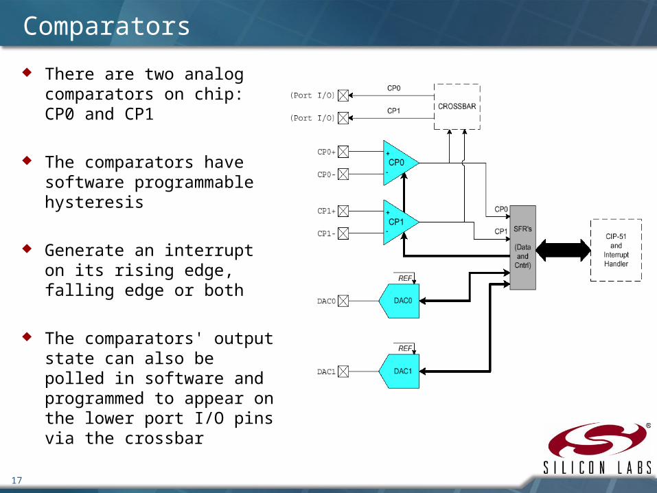
Comparators
There are two analog comparators on chip: CP0 and CP1
The comparators have software programmable hysteresis
Generate an interrupt on its rising edge, falling edge or both
The comparators' output state can also be polled in software and programmed to appear on the lower port I/O pins via the crossbar

18
Voltage Reference for ADC and DAC
A voltage reference has to be used when operating the ADC and DAC
Three external voltage reference input pins: VREF0, VREF1 and VREFD
ADC0 may also reference the DAC0 output internally
ADC1 may also reference the analog power supply voltage (AV+)

19
Internal Voltage Reference Generator
The internal voltage reference circuit consists of a 1.2 V band-gap voltage reference generator and a gain-of-two output buffer amplifier (2.4 V output)
The internal reference may be routed via the VREF pin to external system components or to the voltage reference input pins
The reference control register, REF0CN, enables/disables the internal reference generator and selects the reference inputs for ADC0 and ADC1

www.silabs.com/MCU