lecture 3-layout floorplanningusers.ece.utexas.edu/~mcdermot/vlsi1/main/lectures/lecture_3.pdfstick...
TRANSCRIPT

VLSI-1 Class Notes
Lecture 3:CMOS Layout, Floorplanning & other implementation styles
Mark McDermottElectrical and Computer Engineering
The University of Texas at Austin

VLSI-1 Class Notes
Layout
§ Describes actual layers and geometry on the silicon substrate to implement a function
§ Need to define transistors, interconnection– Transistor widths (for performance)– Spacing, interconnect widths, to reduce defects, satisfy power requirements– Contacts (between poly or active and metal), and vias (between metal
layers)– Wells and their contacts (to power or ground)
§ Layout of lower-level cells constrained by higher-level requirements: floorplanning–
8/26/18 2

VLSI-1 Class Notes
Layout (Cont.)
§ Chips are specified with set of masks
§ Minimum dimensions of masks determine transistor size (and hence speed, cost, and power)
§ Feature size f = distance between source and drain– Set by minimum width of polysilicon
§ Feature size improves 30% every 3 years or so
§ Normalize for feature size when describing design rules
§ Express rules in terms of ll = f/2– E.g. ll = 0.3 µµm in 0.6 µµm process
38/26/18

VLSI-1 Class Notes
CMOS Inverter Layout
48/26/18
SS
DDV
V
Input Output
Note: the N- and P- wellsare not shown here

VLSI-1 Class Notes
Another CMOS Inverter Layout
58/26/18

VLSI-1 Class Notes
CMOS Inverter with Wider Transistors
68/26/18

VLSI-1 Class Notes
Buffer with Two Inverters
78/26/18

VLSI-1 Class Notes
Buffer with Stacked Inverters
88/26/18

VLSI-1 Class Notes
Efficient Buffer with Stacked Inverters
98/26/18

VLSI-1 Class Notes
Simplified Layout of NAND Gate
108/26/18

VLSI-1 Class Notes
Stick Diagram for NAND Gate
118/26/18
§ Identifies actual layers, can be annotated with transistor sizes

VLSI-1 Class Notes
Simplified Design Rules
§ Conservative rules to get you started
128/26/18

VLSI-1 Class Notes
Inverter Layout
§ Transistor dimensions specified as Width / Length– Minimum size 4ll / 2ll,, sometimes called 1 unit or standard pitch– In f = 0.6 µµm process, this is 1.2 µµm wide, 0.6 µµm long
138/26/18

VLSI-1 Class Notes
Typical Layout Densities
§ Typical numbers of high-quality layout§ Derate by 2 for class projects to allow routing and some sloppy
layout.§ Allocate space for big wiring channels
Element AreaRandom logic (2 metal layers) 1000-1500 l2 / transistorDatapath 250 – 750 l2 / transistor
Or 6 WL + 360 l2 / transistorSRAM 1000 l2 / bitDRAM 100 l2 / bitROM 100 l2 / bit
8/26/18 Page 14

VLSI-1 Class Notes
Area Calculation Example: NAND3
§ Horizontal N-diffusion and p-diffusion strips§ Vertical polysilicon gates§ Metal1 VDD rail at top§ Metal1 GND rail at bottom§ 32 ll by 40 ll
8/26/18 Page 15

VLSI-1 Class Notes
Cell Flipping
§ Flip every other cell§ Cells share VDD & GND§ Cells share N-WELL and
substrate connections§ Reduces cell height– Measure contact center to
contact center
Page 168/26/18

VLSI-1 Class Notes
Wiring Tracks
§ A wiring track is the space required for a wire– 4 ll width, 4 ll spacing from neighbor = 8 ll pitch
§ Transistors also consume one wiring track
8/26/18 Page 17
VLSI-1 Class Notes
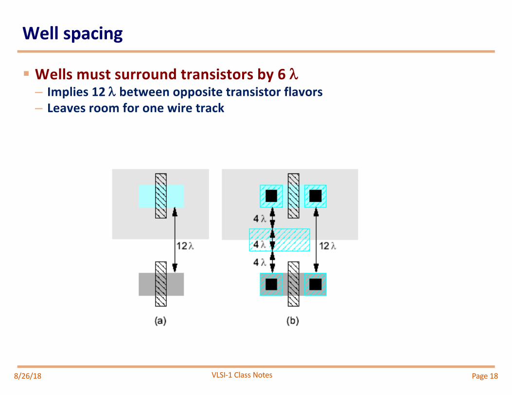
Well spacing
§ Wells must surround transistors by 6 ll– Implies 12 ll between opposite transistor flavors– Leaves room for one wire track
8/26/18 Page 18

VLSI-1 Class Notes
Area Estimation
§ Estimate area by counting wiring tracks– Multiply by 8 to express in ll
8/26/18 Page 19

VLSI-1 Class Notes
Example: O3AI
§ Sketch a stick diagram for O3AI and estimate area
8/26/18
Y = (A + B + C) ¢ D
Page 20

VLSI-1 Class Notes
Example: O3AI
§ Sketch a stick diagram for O3AI and estimate area
8/26/18
Y = (A + B + C) * D
Page 21

VLSI-1 Class Notes
Example: O3AI
§ Sketch a stick diagram for O3AI and estimate area
8/26/18
Y = (A + B + C) * D
Page 22

VLSI-1 Class Notes
The MOSIS Scalable CMOS Rules
§ ll-based rules§ Designs using these rules are fabricated by a variety of companies§ Multiple designs are put on a single die– Each chip wired to a particular design
§ Support for submicron digital CMOS, analog (buried poly layer for capacitor), micromachines, etc.
§ www.mosis.org/Technical/Designrules/scmos/
238/26/18

VLSI-1 Class Notes
Floorplanning
8/26/18 24

VLSI-1 Class Notes
Floorplanning 101
§ Determine block sizes– Function of SC pitch, Cell
Placement, RLM, SC/SDP, Custom/Memory Block Sizing and Block Routing Overhead (Signals, Clocking, Power)
Page 258/26/18

VLSI-1 Class Notes
Floorplanning 101
§ Determine block sizes– Function of SC pitch, Cell Placement, RLM, SC/SDP, Custom/Memory Block
Sizing and Block Routing Overhead (Signals, Clocking, Power)
§ Determine core size– Function of #Blocks, Block sizes, Block Aspect Ratios, Global Routing
Overhead (Signals, Clocking, Power)
§ Determine I/O ring size– Function of the number of I/O, Number of Power Pins and Placement

VLSI-1 Class Notes
Floorplanning
§ How do you estimate block areas?– Begin with block diagram– Each block has
• Inputs• Outputs• Function (draw schematic)• Type: array, datapath, random logic
§ Estimation depends on type of logic– RLM: Random Logic Macro– Datapath– Array

VLSI-1 Class Notes
Area Estimation
§ Arrays:– Layout basic cell– Calculate core area from # of cells– Allow area for decoders, column circuitry
§ Datapaths– Sketch slice plan– Count area of cells from cell library– Ensure wiring is possible
§ Random logic– Compare complexity do a design you have done
8/26/18 Page 28

VLSI-1 Class Notes
Metal Planning
§ Metal layer, width, spacing and shielding are negotiable– “Negotiable” means you have to plead your case to the integration leader– All of these impose a physical constraint for layout
§ Typical 8 layer metal layer allocation– M1,M2 : Local routing (standard cell)– M3,M4, M5, M6 : Data and control– M7,M8 : Power, Ground, Clock, Reset, etc– Assume HVH routing:
• Metal-1: Horizontal• Metal-2: Vertical• Metal-3: Horizontal• Metal-4: Vertical• …..
§ Use standard 'HALO' cells to make the resulting 'floor-plannable' objects 'snap' to the desired power and routing grids.– Added to the boundary of all custom layouts (as well as synthesized blocks).
Page 298/26/18 •29

VLSI-1 Class Notes
Chip & Block Level Clock Routing
§ Watch out for the clock, it’s your most critical net§ Make sure the physical design treats it accordingly§ Help reduce clock power by eliminating unnecessary load§ Make sure the clock net has enough via coverage§ Use a combination of Global (Chip) and Block Level Clock
distribution
Page 308/26/18 •30

VLSI-1 Class Notes
Chip level power routing
§ Power busses are a combination of rings and/or grids.– Rings are generally in the I/O ring. – Grids are used at the chip and block level– Grid pitch is set by horizontal and vertical
routing resource requirements
§ Special consideration needs to be taken for multiple power domains.– There can be any number of power domains
depending on the system architecture– Analog blocks require isolation rings– Interfaces between blocks require level
shifters
Page 318/26/18

VLSI-1 Class Notes
Eye candy: Floorplan examples
8/26/18 Page 32

VLSI-1 Class Notes
Apple A8 SOC (for iPhone)
Page 338/26/18

VLSI-1 Class Notes
Apple A8X SOC (for iPAD)
Page 348/26/18

VLSI-1 Class Notes
Flip chip power mesh for AMD Jaguar
Page 358/26/18
VLSI-1 Class Notes
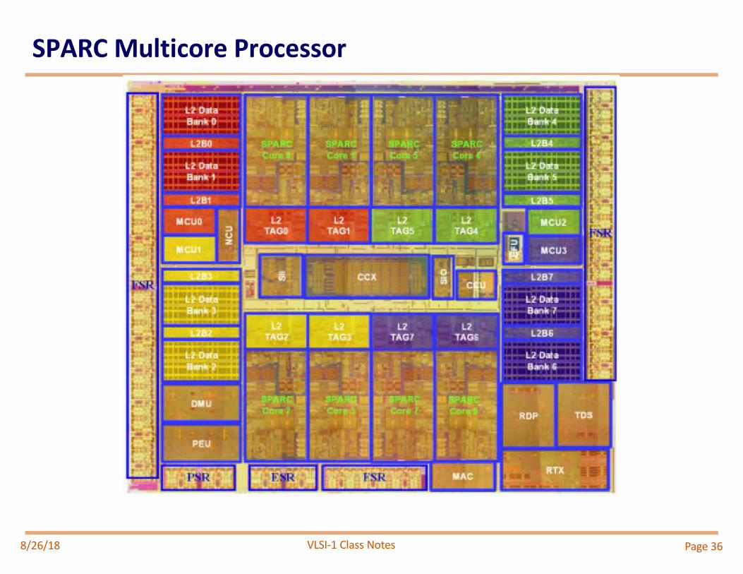
SPARC Multicore Processor
Page 368/26/18

VLSI-1 Class Notes
Xilinx XC2C32A CPLD
Page 378/26/18

VLSI-1 Class Notes
Analog Devices LNA
Page 388/26/18

VLSI-1 Class Notes
Implementation Techniques
8/26/18 39

VLSI-1 Class Notes
Implementation Choices
Custom
Standard CellsCompiled Cells Macro Cells
Cell-based
Pre-diffused(Gate Arrays)
Pre-wired(FPGA's)
Array-based
Semicustom
Digital Circuit Implementation Approaches
8/26/18 40
VLSI-1 Class Notes
RTL Database
Schematic or Gate level RTL
Use RLM library
Create with logic
synthesis
May tweak output by
hand
I want to design
control logic…
Use any existing cell
from the library
Create with text
editor or schematic
capture
I want to design
datapath logic…
LEC
LEC proves
equivalence
of RTL and
Schematics
Create new layout
cells
Create new
schematics
Use new layout cells and
schematic in
Datapath flow to the left
I want to design an
array, complex
dynamic gate,
etc…
Cell LibraryAutomatically Generated Low-Level Netlist
Path from RTL to structural netlist
RLM CUSTOMStructured Datapath
8/26/18 41

VLSI-1 Class Notes
The Custom Approach
Intel 4004
Courtesy Intel© Digital Integrated Circuits2nd
8/26/18 42

VLSI-1 Class Notes
Transition to Automation and Regular Structures
Intel 4004 ( 71)Intel 8080 Intel 8085
Intel 8286Intel 8486Courtesy Intel© Digital Integrated Circuits2nd
8/26/18 43

VLSI-1 Class Notes
Cell-based Design (or standard cells)
Routing channel requirements arereduced by presenceof more interconnectlayers
© Digital Integrated Circuits2nd
8/26/18 44

VLSI-1 Class Notes
Standard Cell — Example
[Brodersen92]
© Digital Integrated Circuits2nd
8/26/18 45
VLSI-1 Class Notes
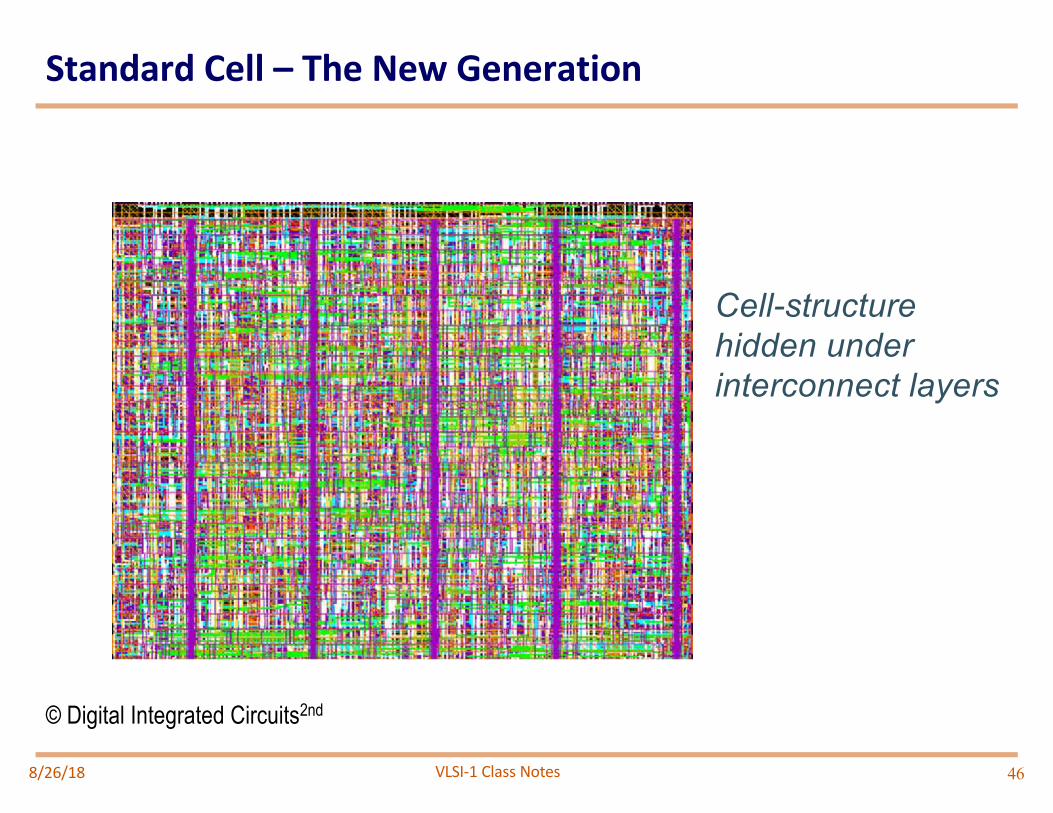
Standard Cell – The New Generation
Cell-structurehidden underinterconnect layers
© Digital Integrated Circuits2nd
8/26/18 46

VLSI-1 Class Notes
Standard Cell - Example
3-input NAND cell(from ST Microelectronics):C = Load capacitanceT = input rise/fall time
© Digital Integrated Circuits2nd
8/26/18 47

VLSI-1 Class Notes
Automatic Cell Generation
Courtesy Cadabra
Initial transistorgeometries
Placedtransistors
Routedcell
Compactedcell
Finishedcell
© Digital Integrated Circuits2nd
8/26/18 48

VLSI-1 Class Notes
MacroModules
256´32 (or 8192 bit) SRAMGenerated by hard-macro module generator
© Digital Integrated Circuits2nd
8/26/18 49

VLSI-1 Class Notes
Soft MacroModules
© Digital Integrated Circuits2nd
8/26/18 50

VLSI-1 Class Notes
Intellectual Property (IP) Cores
A Protocol Processor for Wireless© Digital Integrated Circuits2nd
8/26/18 51

VLSI-1 Class Notes
Semicustom Design Flow
HDL
Logic Synthesis
Floorplanning
Placement
Routing
Tape-out
Circuit Extraction
Pre-Layout Simulation
Post-Layout Simulation
Structural
Physical
BehavioralDesign Capture
Des
ign
Itera
tion
© Digital Integrated Circuits2nd
8/26/18 52

VLSI-1 Class Notes
The Design Closure Problem
Courtesy Synopsys
Iterative Removal of Timing Violations (white lines)
© Digital Integrated Circuits2nd
8/26/18 12. Design Styles 53
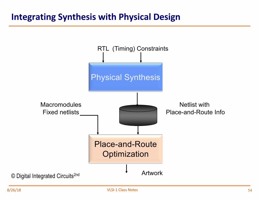
VLSI-1 Class Notes
Integrating Synthesis with Physical Design
Physical Synthesis
RTL (Timing) Constraints
Place-and-RouteOptimization
Artwork
Netlist with Place-and-Route Info
MacromodulesFixed netlists
© Digital Integrated Circuits2nd
8/26/18 54

VLSI-1 Class Notes
Late-Binding Implementation
Pre-diffused(Gate Arrays)
Pre-wired(FPGA's)
Array-based
© Digital Integrated Circuits2nd
8/26/18 55

VLSI-1 Class Notes
Gate Array — Sea-of-gates
rows of
cells
routing channel
uncommitted
VDD
GND
polysilicon
metal
possiblecontact
In1 In2 In3 In4
Out
UncommitedCell
CommittedCell(4-input NOR)
© Digital Integrated Circuits2nd
8/26/18 56

VLSI-1 Class Notes
Sea-of-gate Primitive Cells
NMOS
PMOS
Oxide-isolation
PMOS
NMOS
NMOS
Using oxide-isolation Using gate-isolation
© Digital Integrated Circuits2nd
8/26/18 57

VLSI-1 Class Notes
Example: Base Cell of Gate-Isolated GA
From Smith97© Digital Integrated Circuits2nd
8/26/18 58

VLSI-1 Class Notes
Example: Flip-Flop in Gate-Isolated GA
From Smith97© Digital Integrated Circuits2nd
8/26/18 59

VLSI-1 Class Notes
Sea-of-gates
Random Logic
MemorySubsystem
LSI Logic LEA300K(0.6 µm CMOS)
Courtesy LSI Logic© Digital Integrated Circuits2nd
8/26/18 60

VLSI-1 Class Notes
Prewired Arrays
§ Classification of prewired arrays (or field-programmable devices):– Based on Programming Technique
• Fuse-based (program-once)• Non-volatile EPROM based• RAM based
– Programmable Logic Style• Array-Based• Look-up Table
– Programmable Interconnect Style• Channel-routing• Mesh networks
© Digital Integrated Circuits2nd
8/26/18 Page 61