lecture -36: field effect transistor field effect transistor · lecture -36: field effect...
TRANSCRIPT
Lecture -36: Field Effect Transistor Field Effect Transistor:
The field effect transistor is a semiconductor device, which depends for its operation on the control of current by an electric field. There are two of field effect transistors:
1. JFET (Junction Field Effect Transistor) 2. MOSFET (Metal Oxide Semiconductor Field Effect Transistor)
The FET has several advantages over conventional transistor.
1. In a conventional transistor, the operation depends upon the flow of majority and minority carriers. That is why it is called bipolar transistor. In FET the operation depends upon the flow of majority carriers only. It is called unipolar device.
2. The input to conventional transistor amplifier involves a forward biased PN junction with its inherently low dynamic impedance. The input to FET involves a reverse biased PN junction hence the high input impedance of the order of M-ohm.
3. It is less noisy than a bipolar transistor. 4. It exhibits no offset voltage at zero drain current. 5. It has thermal stability. 6. It is relatively immune to radiation.
The main disadvantage is its relatively small gain bandwidth product in comparison with conventional transistor.
Operation of FET:
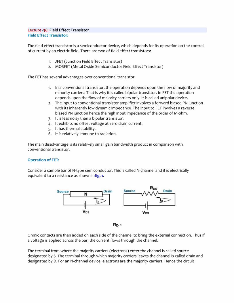
Consider a sample bar of N-type semiconductor. This is called N-channel and it is electrically equivalent to a resistance as shown infig. 1.
Fig. 1
Ohmic contacts are then added on each side of the channel to bring the external connection. Thus if a voltage is applied across the bar, the current flows through the channel.
The terminal from where the majority carriers (electrons) enter the channel is called source designated by S. The terminal through which majority carriers leaves the channel is called drain and designated by D. For an N-channel device, electrons are the majority carriers. Hence the circuit

behaves like a dc voltage VDS applied across a resistance RDS. The resulting current is the drain current ID. If VDS increases, ID increases proportionally.
Now on both sides of the n-type bar heavily doped regions of p-type impurity have been formed by any method for creating pn junction. These impurity regions are called gates (gate1 and gate2) as shown in fig. 2.
Both the gates are internally connected and they are grounded yielding zero gate source voltage (VGS =0). The word gate is used because the potential applied between gate and source controls the channel width and hence the current.
As with all PN junctions, a depletion region is formed on the two sides of the reverse biased PN junction. The current carriers have diffused across the junction, leaving only uncovered positive ions on the n side and negative ions on the p side. The depletion region width increases with the magnitude of reverse bias. The conductivity of this channel is normally zero because of the unavailability of current carriers.
The potential at any point along the channel depends on the distance of that point from the drain, points close to the drain are at a higher positive potential, relative to ground, then points close to the source. Both depletion regions are therefore subject to greater reverse voltage near the drain. Therefore the depletion region width increases as we move towards drain. The flow of electrons from source to drain is now restricted to the narrow channel between the no conducting depletion regions. The width of this channel determines the resistance between drain and source.
Fig. 2
Consider now the behavior of drain current ID vs drain source voltage VDS. The gate source voltage is zero therefore VGS= 0. Suppose that VDS is gradually linearly increased linearly from 0V. ID also increases.

Since the channel behaves as a semiconductor resistance, therefore it follows ohm's law. The region is called ohmic region, with increasing current, the ohmic voltage drop between the source and the channel region reverse biased the junction, the conducting portion of the channel begins to constrict and ID begins to level off until a specific value of VDSis reached, called the pinch of voltage VP.
At this point further increase in VDS do not produce corresponding increase in ID. Instead, as VDS increases, both depletion regions extend further into the channel, resulting in a no more cross section, and hence a higher channel resistance. Thus even though, there is more voltage, the resistance is also greater and the current remains relatively constant. This is called pinch off or saturation region. The current in this region is maximum current that FET can produce and designated by IDSS. (Drain to source current with gate shorted).
Fig. 3
As with all pn junctions, when the reverse voltage exceeds a certain level, avalanche breakdown of pn junction occurs and ID rises very rapidly as shown in fig. 3.
Consider now an N-channel JFET with a reverse gate source voltage as shown in fig. 4.
Fig. 4
Fig. 5
The additional reverse bias, pinch off will occur for smaller values of | VDS |, and the maximum drain current will be smaller. A family of curves for different values of VGS(negative) is shown in fig. 5.
Suppose that VGS= 0 and that due of VDS at a specific point along the channel is +5V with respect to ground. Therefore reverse voltage across either p-n junction is now 5V. If VGS is decreased from 0 to –
1V the net reverse bias near the point is 5 - (-1) = 6V. Thus for any fixed value of VDS, the channel width decreases as VGS is made more negative.
Thus ID value changes correspondingly. When the gate voltage is negative enough, the depletion layers touch each other and the conducting channel pinches off (disappears). In this case the drain current is cut off. The gate voltage that produces cut off is symbolized VGS(off) . It is same as pinch off voltage.
Since the gate source junction is a reverse biased silicon diode, only a very small reverse current flows through it. Ideally gate current is zero. As a result, all the free electrons from the source go to the drain i.e. ID = IS. Because the gate draws almost negligible reverse current the input resistance is very high 10's or 100's of M ohm. Therefore where high input impedance is required, JFET is preferred over BJT. The disadvantage is less control over output current i.e. FET takes larger changes in input voltage to produce changes in output current. For this reason, JFET has less voltage gain than a bipolar amplifier.
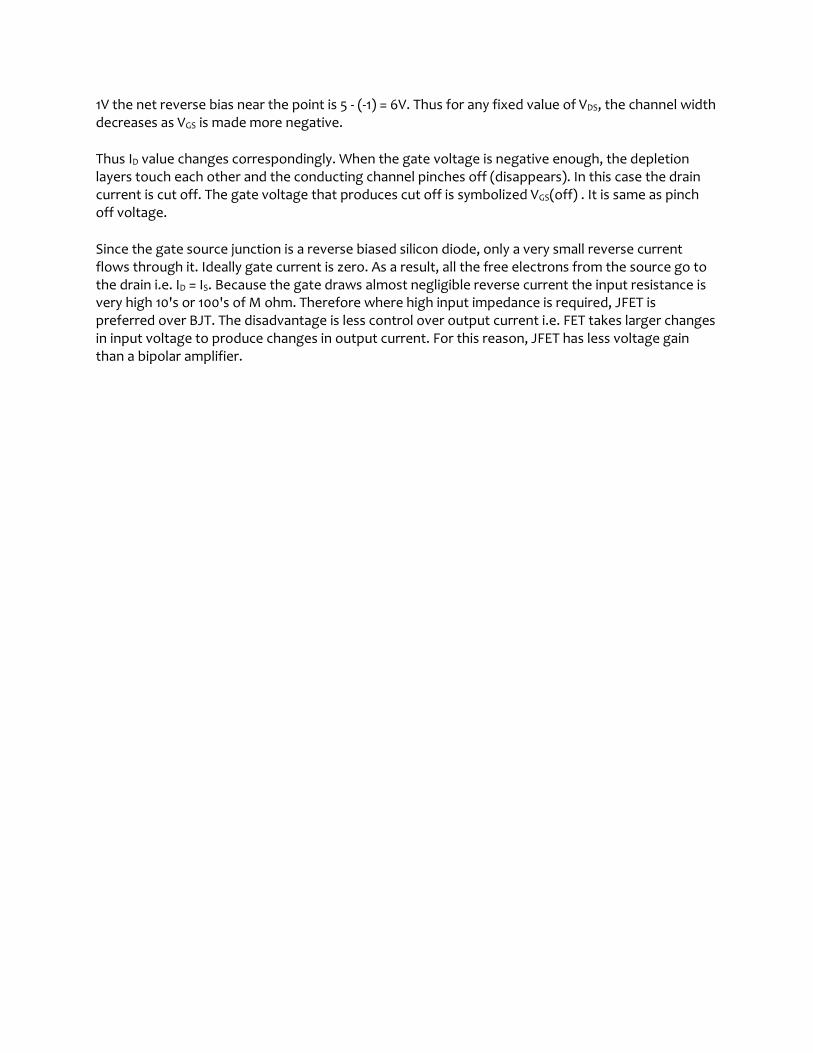
Lecture -37: Biasing the Field Effect Transistor Transductance Curves:
The transductance curve of a JFET is a graph of output current (ID) vs input voltage (VGS) as shown in fig. 1.
Fig. 1
By reading the value of ID and VGS for a particular value of VDS, the transductance curve can be plotted. The transductance curve is a part of parabola. It has an equation of
Data sheet provides only IDSS and VGS(off) value. Using these values the transductance curve can be plotted.
Biasing the FET:
The FET can be biased as an amplifier. Consider the common source drain characteristic of a JFET. For linear amplification, Q point must be selected somewhere in the saturation region. Q point is selected on the basis of ac performance i.e. gain, frequency response, noise, power, current and voltage ratings.
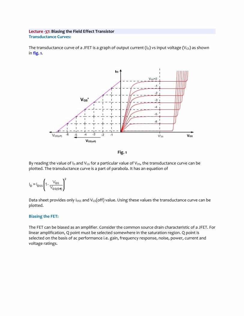
Gate Bias:
Fig. 2, shows a simple gate bias circuit.
Fig. 2
Separate VGS supply is used to set up Q point. This is the worst way to select Q point. The reason is that there is considerable variation between the maximum and minimum values of FET parameters e.g.
IDSS VGS(off)
Minimum 4mA -2V
Maximum 13mA -8V
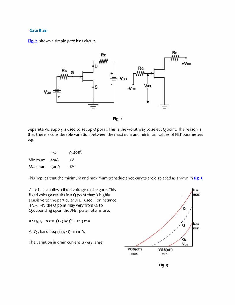
This implies that the minimum and maximum transductance curves are displaced as shown in fig. 3.
Gate bias applies a fixed voltage to the gate. This fixed voltage results in a Q point that is highly sensitive to the particular JFET used. For instance, if VGS= -1V the Q point may very from Q1 to Q2depending upon the JFET parameter is use.
At Q1, ID= 0.016 (1 - (1/8))2 = 12.3 mA
At Q2, ID= 0.004 (1-(1/2))2 = 1 mA.
The variation in drain current is very large.
Fig. 3
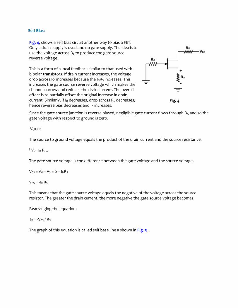
Self Bias:
Fig. 4, shows a self bias circuit another way to bias a FET. Only a drain supply is used and no gate supply. The idea is to use the voltage across RS to produce the gate source reverse voltage.
This is a form of a local feedback similar to that used with bipolar transistors. If drain current increases, the voltage drop across RS increases because the IDRS increases. This increases the gate source reverse voltage which makes the channel narrow and reduces the drain current. The overall effect is to partially offset the original increase in drain current. Similarly, if ID decreases, drop across RS decreases, hence reverse bias decreases and ID increases.
Fig. 4
Since the gate source junction is reverse biased, negligible gate current flows through RG and so the gate voltage with respect to ground is zero.
VG= 0;
The source to ground voltage equals the product of the drain current and the source resistance.
\ VS= ID R S.
The gate source voltage is the difference between the gate voltage and the source voltage.
VGS = VG – VS = 0 – IDRS
VGS = -ID RS.
This means that the gate source voltage equals the negative of the voltage across the source resistor. The greater the drain current, the more negative the gate source voltage becomes.
Rearranging the equation:
ID = -VGS / RS
The graph of this equation is called self base line a shown in Fig. 5.
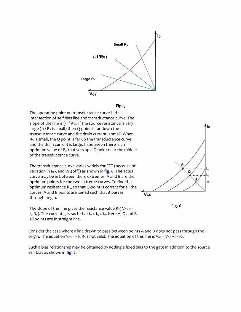
Fig. 5
The operating point on transductance curve is the intersection of self bias line and transductance curve. The slope of the line is (-1 / RS). If the source resistance is very large (-1 / RS is small) then Q-point is far down the transductance curve and the drain current is small. When RS is small, the Q point is far up the transductance curve and the drain current is large. In between there is an optimum value of RS that sets up a Q point near the middle of the transductance curve.
The transductance curve varies widely for FET (because of variation in IDSS and VGS(off)) as shown in fig. 6. The actual curve may be in between there extremes. A and B are the optimum points for the two extreme curves. To find the optimum resistance RS, so that Q-point is correct for all the curves, A and B points are joined such that it passes through origin.
The slope of this line gives the resistance value RS( VGS = -ID RS). The current IQ is such that IA > IQ > IB. Here A, Q and B all points are in straight line.
Fig. 6
Consider the case where a line drawn to pass between points A and B does not pass through the origin. The equation VGS = - ID RSis not valid. The equation of this line is VGS = VGG – ID RS.
Such a bias relationship may be obtained by adding a fixed bias to the gate in addition to the source self bias as shown in fig. 7.
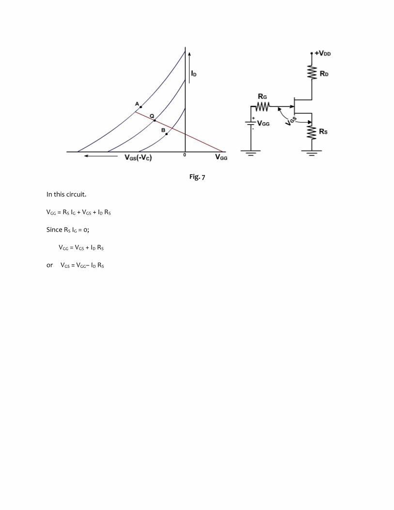
Fig. 7
In this circuit.
VGG = RS IG + VGS + ID RS
Since RS IG = 0;
VGG = VGS + ID RS
or VGS = VGG– ID RS
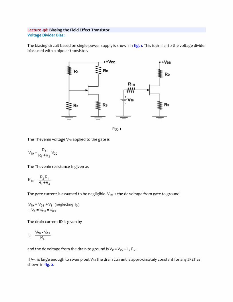
Lecture -38: Biasing the Field Effect Transistor Voltage Divider Bias :
The biasing circuit based on single power supply is shown in fig. 1. This is similar to the voltage divider bias used with a bipolar transistor.
Fig. 1
The Thevenin voltage VTH applied to the gate is
The Thevenin resistance is given as
The gate current is assumed to be negligible. VTH is the dc voltage from gate to ground.
The drain current ID is given by
and the dc voltage from the drain to ground is VD = VDD – ID RD.
If VTH is large enough to swamp out VGS the drain current is approximately constant for any JFET as shown in fig. 2.
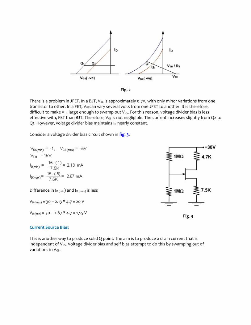
Fig. 2
There is a problem in JFET. In a BJT, VBE is approximately 0.7V, with only minor variations from one transistor to other. In a FET, VGScan vary several volts from one JFET to another. It is therefore, difficult to make VTH large enough to swamp out VGS. For this reason, voltage divider bias is less effective with, FET than BJT. Therefore, VGS is not negligible. The current increases slightly from Q2 to Q1. However, voltage divider bias maintains ID nearly constant.
Consider a voltage divider bias circuit shown in fig. 3.
Difference in ID (min) and ID (max) is less
VD (max) = 30 – 2.13 * 4.7 = 20 V
VD (min) = 30 – 2.67 * 4.7 = 17.5 V
Fig. 3
Current Source Bias:
This is another way to produce solid Q point. The aim is to produce a drain current that is independent of VGS. Voltage divider bias and self bias attempt to do this by swamping out of variations in VGS.
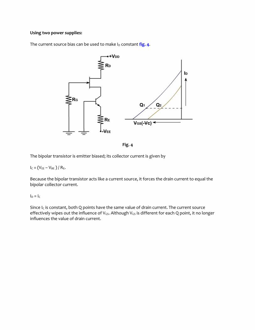
Using two power supplies:
The current source bias can be used to make ID constant fig. 4.
Fig. 4
The bipolar transistor is emitter biased; its collector current is given by
IC = (VEE – VBE ) / RE.
Because the bipolar transistor acts like a current source, it forces the drain current to equal the bipolar collector current.
ID = IC
Since IC is constant, both Q points have the same value of drain current. The current source effectively wipes out the influence of VGS. Although VGS is different for each Q point, it no longer influences the value of drain current.
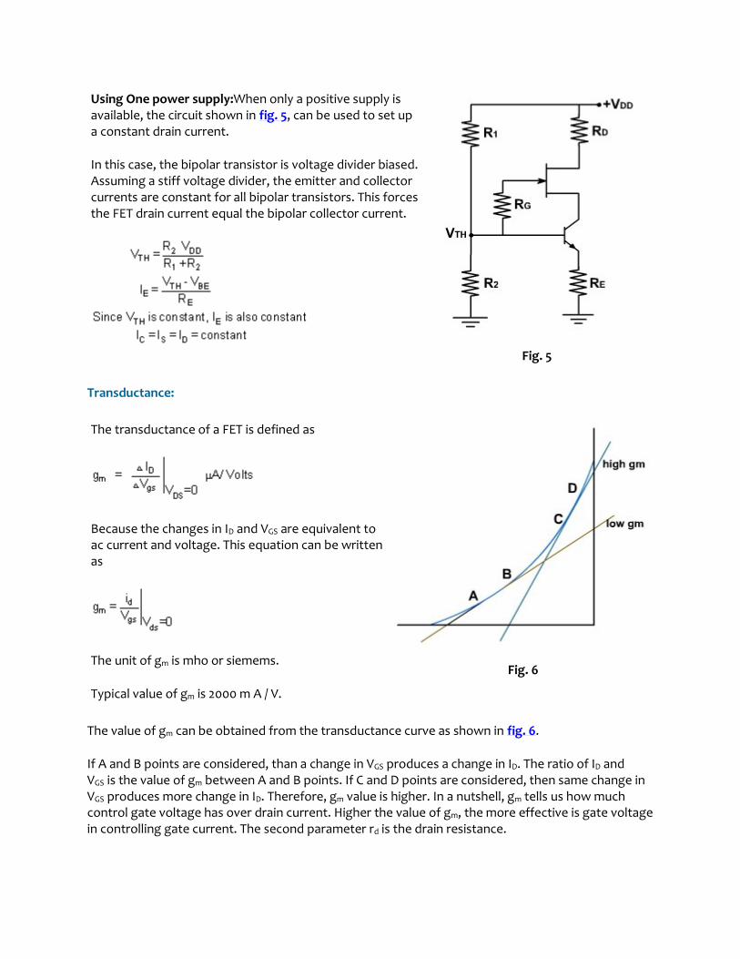
Using One power supply:When only a positive supply is available, the circuit shown in fig. 5, can be used to set up a constant drain current.
In this case, the bipolar transistor is voltage divider biased. Assuming a stiff voltage divider, the emitter and collector currents are constant for all bipolar transistors. This forces the FET drain current equal the bipolar collector current.
Fig. 5
Transductance:
The transductance of a FET is defined as
Because the changes in ID and VGS are equivalent to ac current and voltage. This equation can be written as
The unit of gm is mho or siemems.
Typical value of gm is 2000 m A / V.
Fig. 6
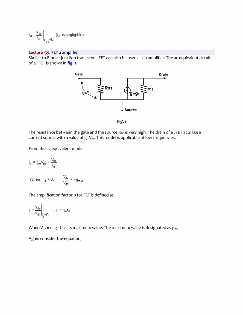
The value of gm can be obtained from the transductance curve as shown in fig. 6.
If A and B points are considered, than a change in VGS produces a change in ID. The ratio of ID and VGS is the value of gm between A and B points. If C and D points are considered, then same change in VGS produces more change in ID. Therefore, gm value is higher. In a nutshell, gm tells us how much control gate voltage has over drain current. Higher the value of gm, the more effective is gate voltage in controlling gate current. The second parameter rd is the drain resistance.
Lecture -39: FET a amplifier Similar to Bipolar junction transistor. JFET can also be used as an amplifier. The ac equivalent circuit of a JFET is shown in fig. 1.
Fig. 1
The resistance between the gate and the source RGS is very high. The drain of a JFET acts like a current source with a value of gmVgs. This model is applicable at low frequencies.
From the ac equivalent model
The amplification factor µ for FET is defined as
When VGS = 0, gm has its maximum value. The maximum value is designated as gmo.
Again consider the equation,
As VGS increases, gm decreases linearly.
Measuring IDSS and gm, VGS(off) can be determined
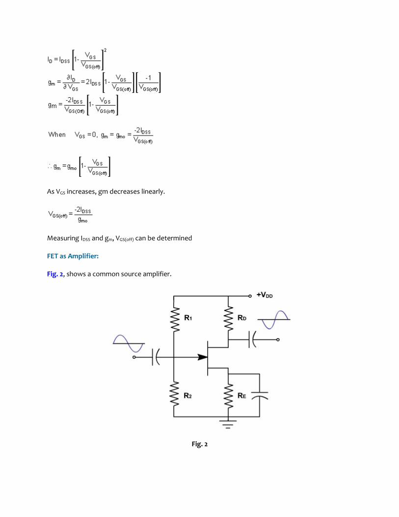
FET as Amplifier:
Fig. 2, shows a common source amplifier.
Fig. 2
When a small ac signal is coupled into the gate it produces variations in gate source voltage. This produces a sinusoidal drain current. Since an ac current flows through the drain resistor. An amplified ac voltage is obtained at the output. An increase in gate source voltage produces more drain current, which means that the drain voltage is decreasing. Since the positive half cycle of input voltage produces the negative half cycle of output voltage, we get phase inversion in a CS amplifier.
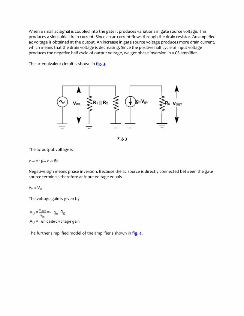
The ac equivalent circuit is shown in fig. 3.
Fig. 3
The ac output voltage is
vout = - gm v gS RD
Negative sign means phase inversion. Because the ac source is directly connected between the gate source terminals therefore ac input voltage equals
Vin = Vgs
The voltage gain is given by
The further simplified model of the amplifieris shown in fig. 4.
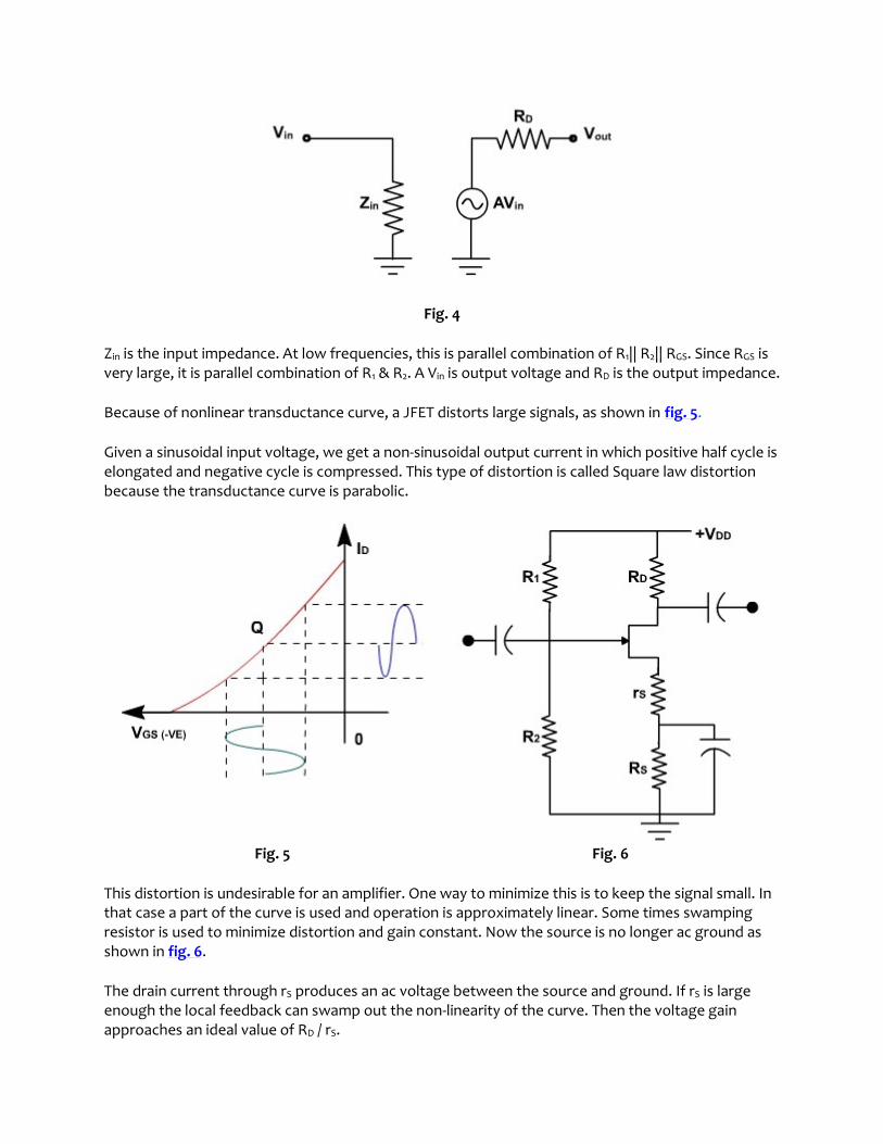
Fig. 4
Zin is the input impedance. At low frequencies, this is parallel combination of R1|| R2|| RGS. Since RGS is very large, it is parallel combination of R1 & R2. A Vin is output voltage and RD is the output impedance.
Because of nonlinear transductance curve, a JFET distorts large signals, as shown in fig. 5.
Given a sinusoidal input voltage, we get a non-sinusoidal output current in which positive half cycle is elongated and negative cycle is compressed. This type of distortion is called Square law distortion because the transductance curve is parabolic.
Fig. 5 Fig. 6
This distortion is undesirable for an amplifier. One way to minimize this is to keep the signal small. In that case a part of the curve is used and operation is approximately linear. Some times swamping resistor is used to minimize distortion and gain constant. Now the source is no longer ac ground as shown in fig. 6.
The drain current through rS produces an ac voltage between the source and ground. If rS is large enough the local feedback can swamp out the non-linearity of the curve. Then the voltage gain approaches an ideal value of RD / rS.
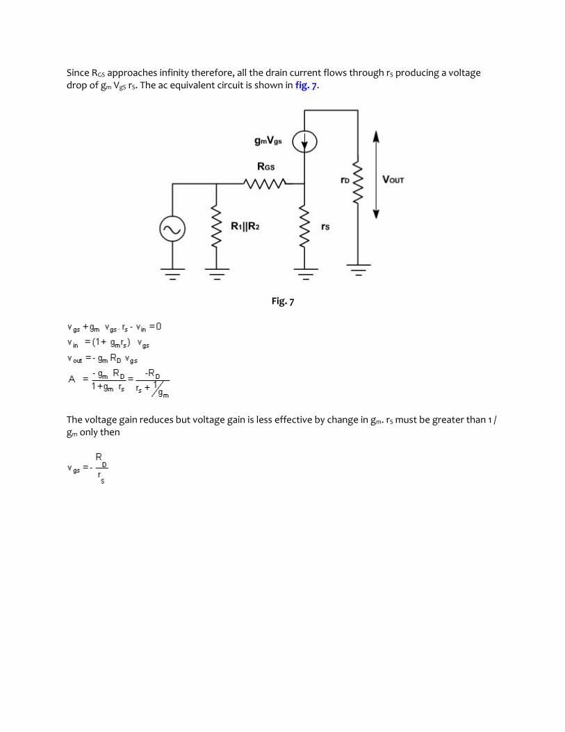
Since RGS approaches infinity therefore, all the drain current flows through rS producing a voltage drop of gm VgS rS. The ac equivalent circuit is shown in fig. 7.
Fig. 7
The voltage gain reduces but voltage gain is less effective by change in gm. rS must be greater than 1 / gm only then
Lecture - 40: JFET Applications Example-1:
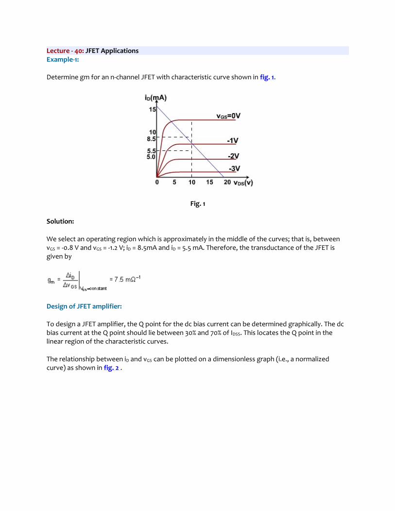
Determine gm for an n-channel JFET with characteristic curve shown in fig. 1.
Fig. 1
Solution:
We select an operating region which is approximately in the middle of the curves; that is, between vGS = -0.8 V and vGS = -1.2 V; iD = 8.5mA and iD = 5.5 mA. Therefore, the transductance of the JFET is given by
Design of JFET amplifier:
To design a JFET amplifier, the Q point for the dc bias current can be determined graphically. The dc bias current at the Q point should lie between 30% and 70% of IDSS. This locates the Q point in the linear region of the characteristic curves.
The relationship between iD and vGS can be plotted on a dimensionless graph (i.e., a normalized curve) as shown in fig. 2 .
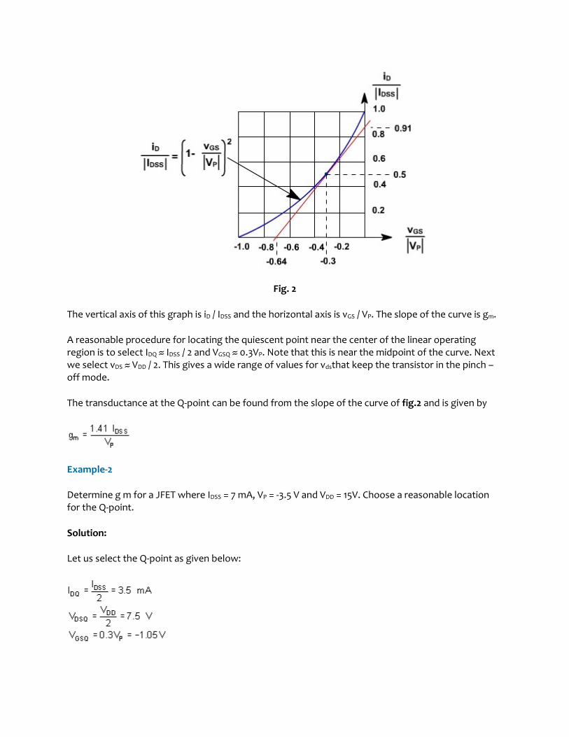
Fig. 2
The vertical axis of this graph is iD / IDSS and the horizontal axis is vGS / VP. The slope of the curve is gm.
A reasonable procedure for locating the quiescent point near the center of the linear operating region is to select IDQ ≈ IDSS / 2 and VGSQ ≈ 0.3VP. Note that this is near the midpoint of the curve. Next we select vDS ≈ VDD / 2. This gives a wide range of values for vdsthat keep the transistor in the pinch –off mode.
The transductance at the Q-point can be found from the slope of the curve of fig.2 and is given by
Example-2
Determine g m for a JFET where IDSS = 7 mA, VP = -3.5 V and VDD = 15V. Choose a reasonable location for the Q-point.
Solution:
Let us select the Q-point as given below:
The transconductance, gm, is found from the slope of the curve at the point iD / IDSS = 0.5 and vGS / VP =0.3. Hence,
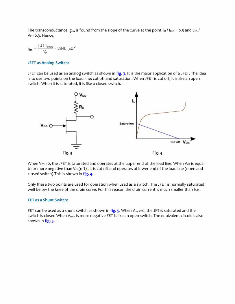
JEFT as Analog Switch:
JFET can be used as an analog switch as shown in fig. 3. It is the major application of a JFET. The idea is to use two points on the load line: cut off and saturation. When JFET is cut off, it is like an open switch. When it is saturated, it is like a closed switch.
Fig. 3 Fig. 4
When VGS =0, the JFET is saturated and operates at the upper end of the load line. When VGS is equal to or more negative than VGS(off) , it is cut off and operates at lower end of the load line (open and closed switch).This is shown in fig. 4.
Only these two points are used for operation when used as a switch. The JFET is normally saturated well below the knee of the drain curve. For this reason the drain current is much smaller than IDSS .
FET as a Shunt Switch:
FET can be used as a shunt switch as shown in fig. 5. When Vcont=0, the JFT is saturated and the switch is closed When Vcont is more negative FET is like an open switch. The equivalent circuit is also shown in fig. 5.
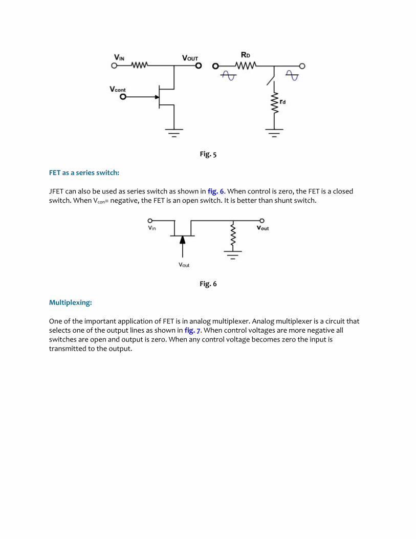
Fig. 5
FET as a series switch:
JFET can also be used as series switch as shown in fig. 6. When control is zero, the FET is a closed switch. When Vcon= negative, the FET is an open switch. It is better than shunt switch.
Fig. 6
Multiplexing:
One of the important application of FET is in analog multiplexer. Analog multiplexer is a circuit that selects one of the output lines as shown in fig. 7. When control voltages are more negative all switches are open and output is zero. When any control voltage becomes zero the input is transmitted to the output.

Fig. 7