lecture 6: integrated circuit resistors
DESCRIPTION
Lecture 6: Integrated Circuit Resistors. Prof. Niknejad. Lecture Outline. Semiconductors Si Diamond Structure Bond Model Intrinsic Carrier Concentration Doping by Ion Implantation Drift Velocity Saturation IC Process Flow Resistor Layout Diffusion. - PowerPoint PPT PresentationTRANSCRIPT
Department of EECS University of California, Berkeley
EECS 105 Fall 2003, Lecture 6
Lecture 6: Integrated Circuit Resistors
Prof. Niknejad
Department of EECS University of California, Berkeley
EECS 105 Fall 2003, Lecture 6 Prof. A. Niknejad
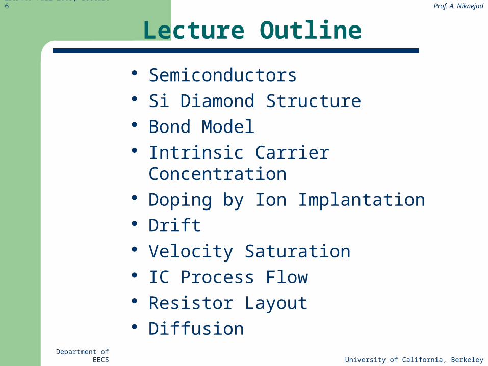
Lecture Outline
Semiconductors Si Diamond Structure Bond Model Intrinsic Carrier Concentration Doping by Ion Implantation Drift Velocity Saturation IC Process Flow Resistor Layout Diffusion
Department of EECS University of California, Berkeley
EECS 105 Fall 2003, Lecture 6 Prof. A. Niknejad
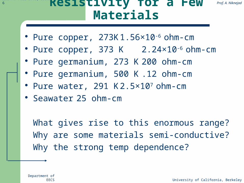
Resistivity for a Few Materials
Pure copper, 273K 1.56×10⁻⁶ ohm-cm Pure copper, 373 K 2.24×10⁻⁶ ohm-cm Pure germanium, 273 K 200 ohm-cm Pure germanium, 500 K .12 ohm-cm Pure water, 291 K 2.5×10⁷ ohm-cm Seawater 25 ohm-cm
What gives rise to this enormous range?
Why are some materials semi-conductive?
Why the strong temp dependence?

Department of EECS University of California, Berkeley
EECS 105 Fall 2003, Lecture 6 Prof. A. Niknejad
Electronic Properties of Silicon
Silicon is in Group IV – Atom electronic structure: 1s22s22p63s23p2
– Crystal electronic structure: 1s22s22p63(sp)4
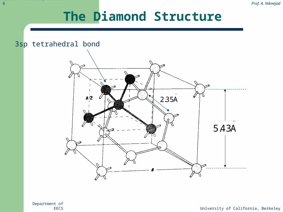
– Diamond lattice, with 0.235 nm bond length Very poor conductor at room temperature:
why?(1s)2
(2s)2
(2p)6 (3sp)4
Hybridized State
Department of EECS University of California, Berkeley
EECS 105 Fall 2003, Lecture 6 Prof. A. Niknejad
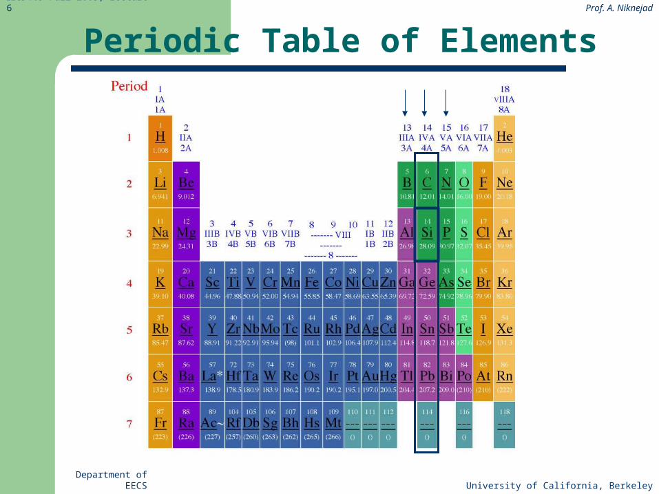
Periodic Table of Elements
Department of EECS University of California, Berkeley
EECS 105 Fall 2003, Lecture 6 Prof. A. Niknejad
The Diamond Structure
3sp tetrahedral bond
A43.5
A35.2
Department of EECS University of California, Berkeley
EECS 105 Fall 2003, Lecture 6 Prof. A. Niknejad
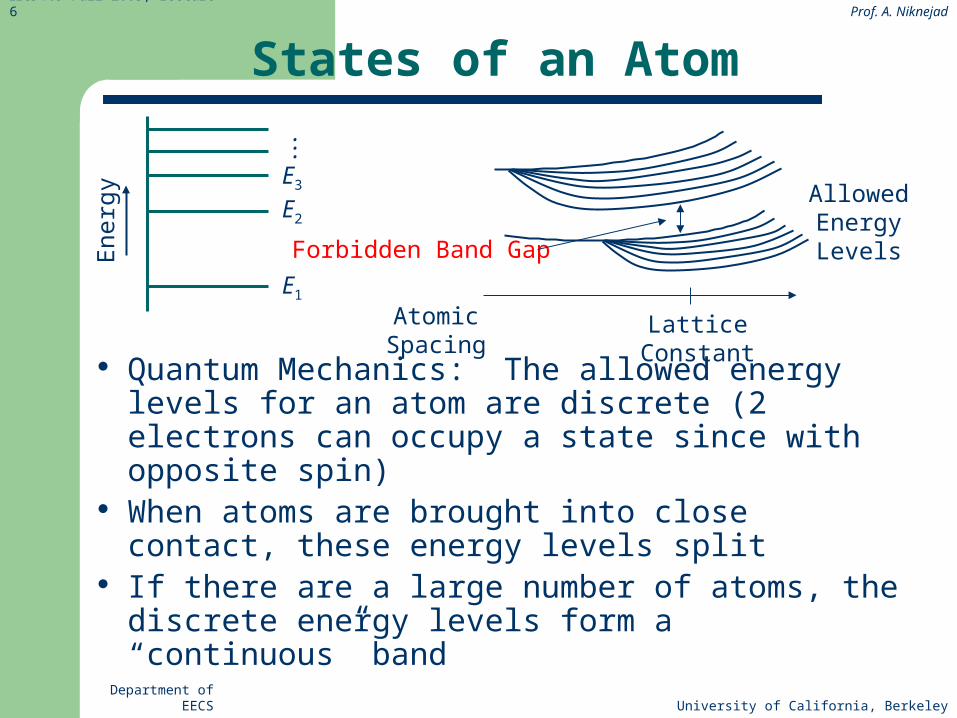
States of an Atom
Quantum Mechanics: The allowed energy levels for an atom are discrete (2 electrons can occupy a state since with opposite spin)
When atoms are brought into close contact, these energy levels split
If there are a large number of atoms, the discrete energy levels form a “continuous” band
Ene
rgy
E1
E2
...E3
Forbidden Band Gap
AllowedEnergyLevels
Lattice ConstantAtomic Spacing
Department of EECS University of California, Berkeley
EECS 105 Fall 2003, Lecture 6 Prof. A. Niknejad
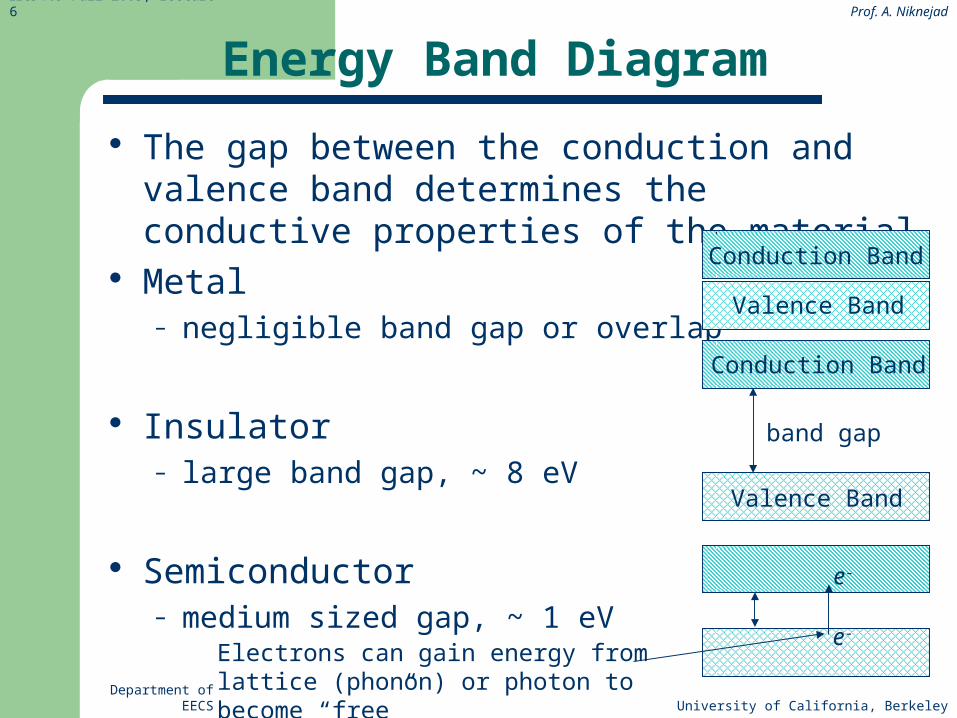
Energy Band Diagram
The gap between the conduction and valence band determines the conductive properties of the material
Metal– negligible band gap or overlap
Insulator – large band gap, ~ 8 eV
Semiconductor– medium sized gap, ~ 1 eV
Valence Band
Conduction Band
Valence Band
Conduction Band
e-
Electrons can gain energy from lattice (phonon) or photon to become “free”
band gap
e-
Department of EECS University of California, Berkeley
EECS 105 Fall 2003, Lecture 6 Prof. A. Niknejad
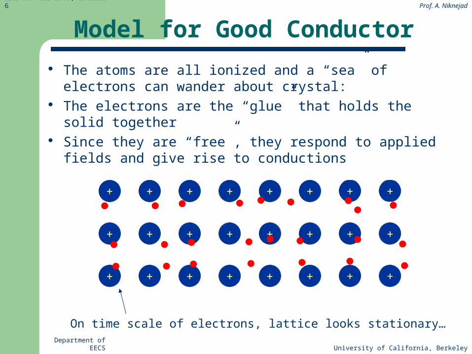
Model for Good Conductor
The atoms are all ionized and a “sea” of electrons can wander about crystal:
The electrons are the “glue” that holds the solid together Since they are “free”, they respond to applied fields and
give rise to conductions
+ + + + + + + +
+ + + + + + + +
+ + + + + + + +
On time scale of electrons, lattice looks stationary…
Department of EECS University of California, Berkeley
EECS 105 Fall 2003, Lecture 6 Prof. A. Niknejad
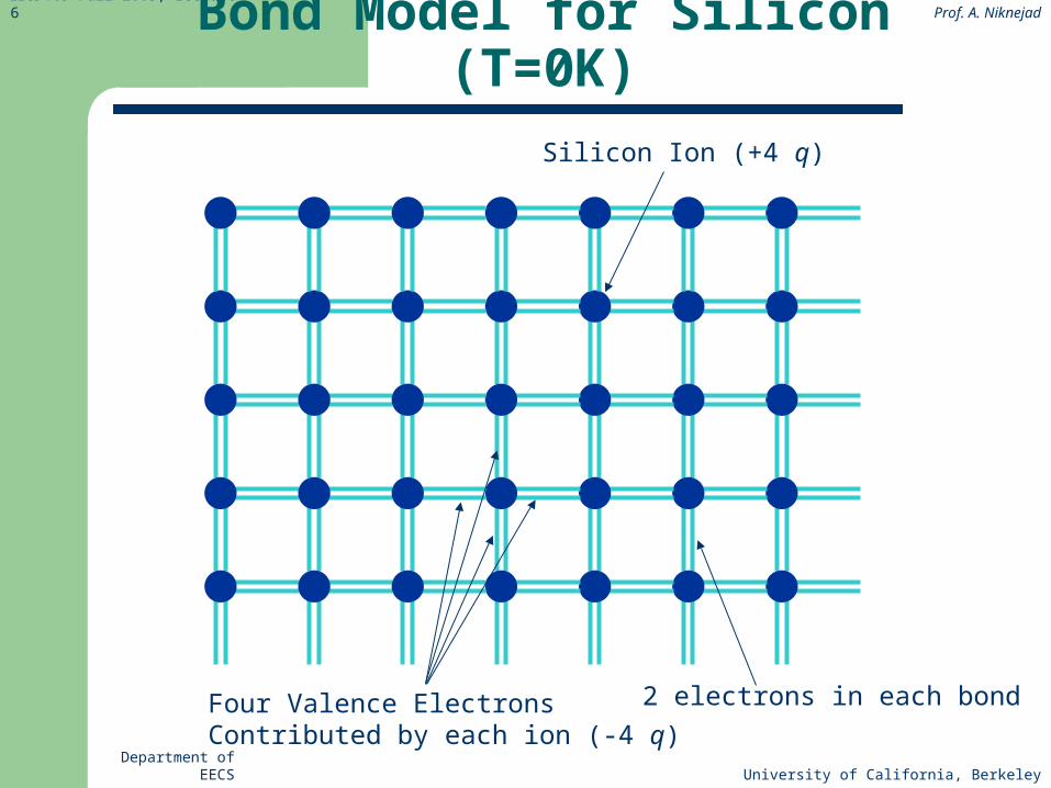
Bond Model for Silicon (T=0K)
Silicon Ion (+4 q)
Four Valence ElectronsContributed by each ion (-4 q)
2 electrons in each bond
Department of EECS University of California, Berkeley
EECS 105 Fall 2003, Lecture 6 Prof. A. Niknejad
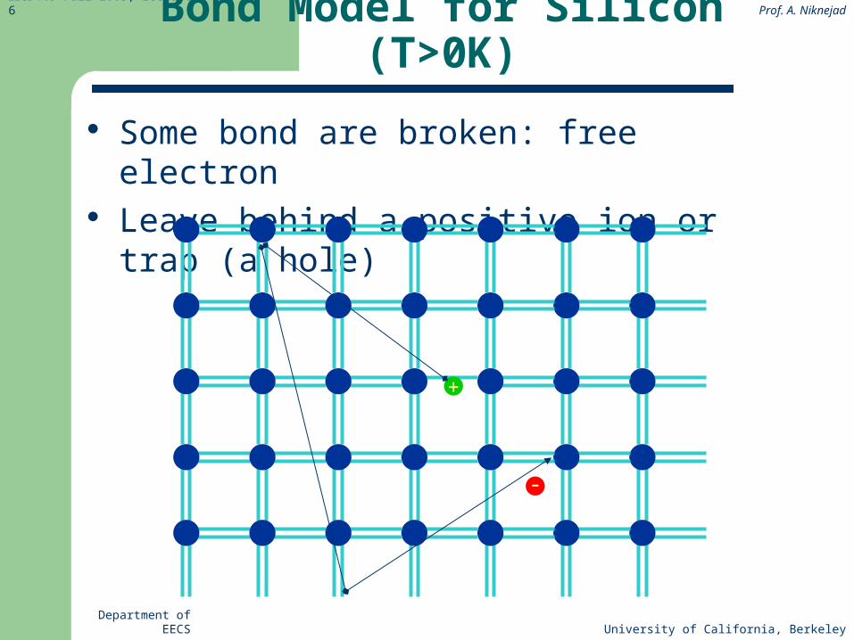
Bond Model for Silicon (T>0K)
Some bond are broken: free electron Leave behind a positive ion or trap (a hole)
+
-
Department of EECS University of California, Berkeley
EECS 105 Fall 2003, Lecture 6 Prof. A. Niknejad
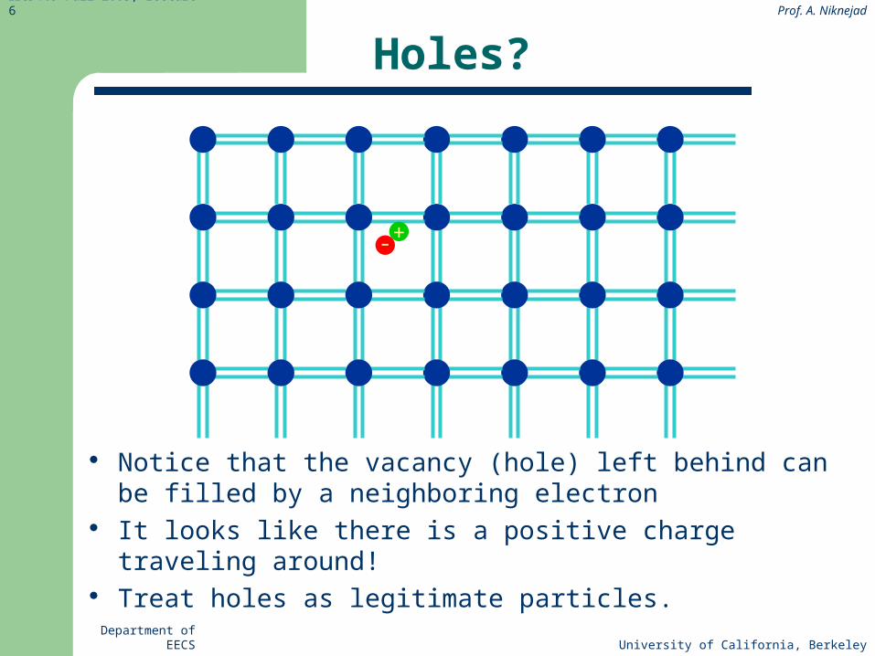
Holes?
Notice that the vacancy (hole) left behind can be filled by a neighboring electron
It looks like there is a positive charge traveling around! Treat holes as legitimate particles.
+-
Department of EECS University of California, Berkeley
EECS 105 Fall 2003, Lecture 6 Prof. A. Niknejad
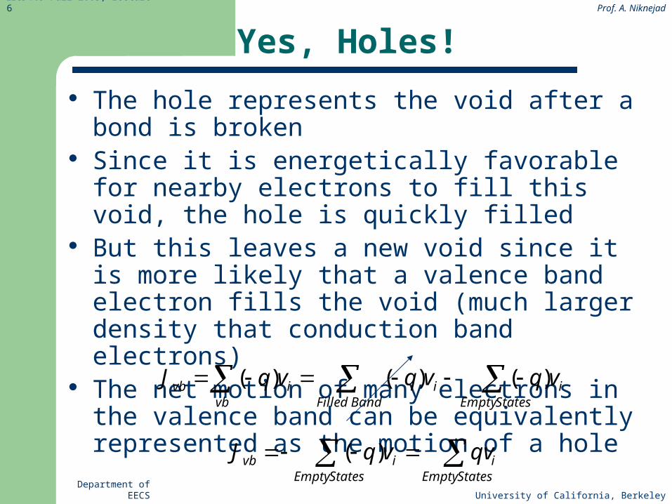
Yes, Holes!
The hole represents the void after a bond is broken Since it is energetically favorable for nearby
electrons to fill this void, the hole is quickly filled But this leaves a new void since it is more likely
that a valence band electron fills the void (much larger density that conduction band electrons)
The net motion of many electrons in the valence band can be equivalently represented as the motion of a hole
BandFilled StatesEmpty
iivb
ivb vqvqvqJ )()()(
StatesEmpty
iStatesEmpty
ivb qvvqJ )(
Department of EECS University of California, Berkeley
EECS 105 Fall 2003, Lecture 6 Prof. A. Niknejad
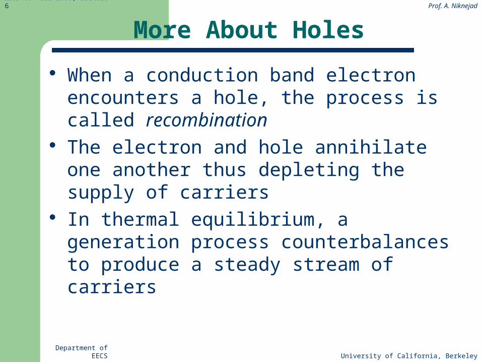
More About Holes
When a conduction band electron encounters a hole, the process is called recombination
The electron and hole annihilate one another thus depleting the supply of carriers
In thermal equilibrium, a generation process counterbalances to produce a steady stream of carriers
Department of EECS University of California, Berkeley
EECS 105 Fall 2003, Lecture 6 Prof. A. Niknejad
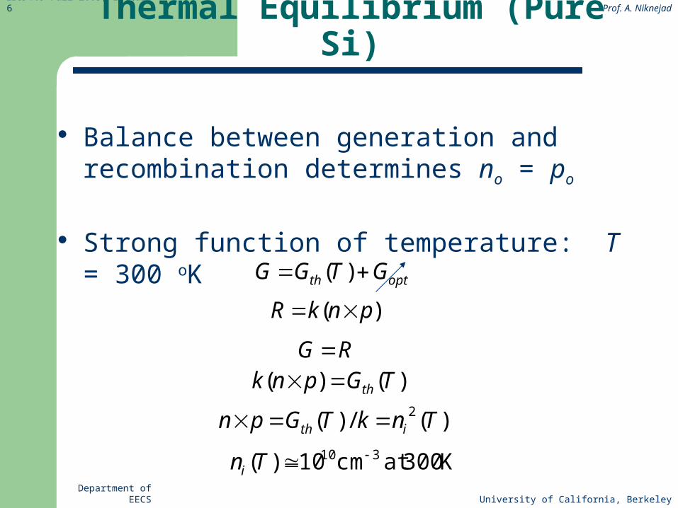
Thermal Equilibrium (Pure Si)
Balance between generation and recombination determines no = po
Strong function of temperature: T = 300 oKoptth GTGG )(
)( pnkR
RG )()( TGpnk th
)(/)( 2 TnkTGpn ith
K300atcm10)( 310 Tni
Department of EECS University of California, Berkeley
EECS 105 Fall 2003, Lecture 6 Prof. A. Niknejad
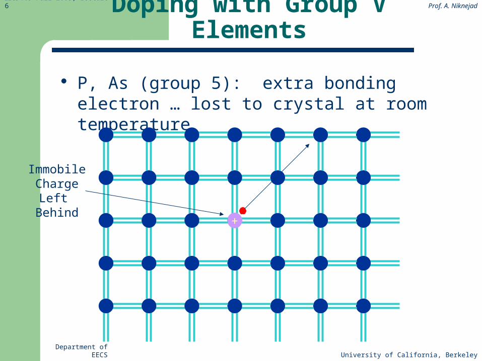
Doping with Group V Elements
P, As (group 5): extra bonding electron … lost to crystal at room temperature
+
ImmobileCharge
Left Behind

Department of EECS University of California, Berkeley
EECS 105 Fall 2003, Lecture 6 Prof. A. Niknejad
Donor Accounting
Each ionized donor will contribute an extra “free” electron
The material is charge neutral, so the total charge concentration must sum to zero:
By Mass-Action Law:
000 dqNqpqn
Free Electrons
Free Holes
Ions(Immobile)
)(2 Tnpn i
00
2
0 di qN
n
nqqn
0022
0 nqNqnqn di
Department of EECS University of California, Berkeley
EECS 105 Fall 2003, Lecture 6 Prof. A. Niknejad
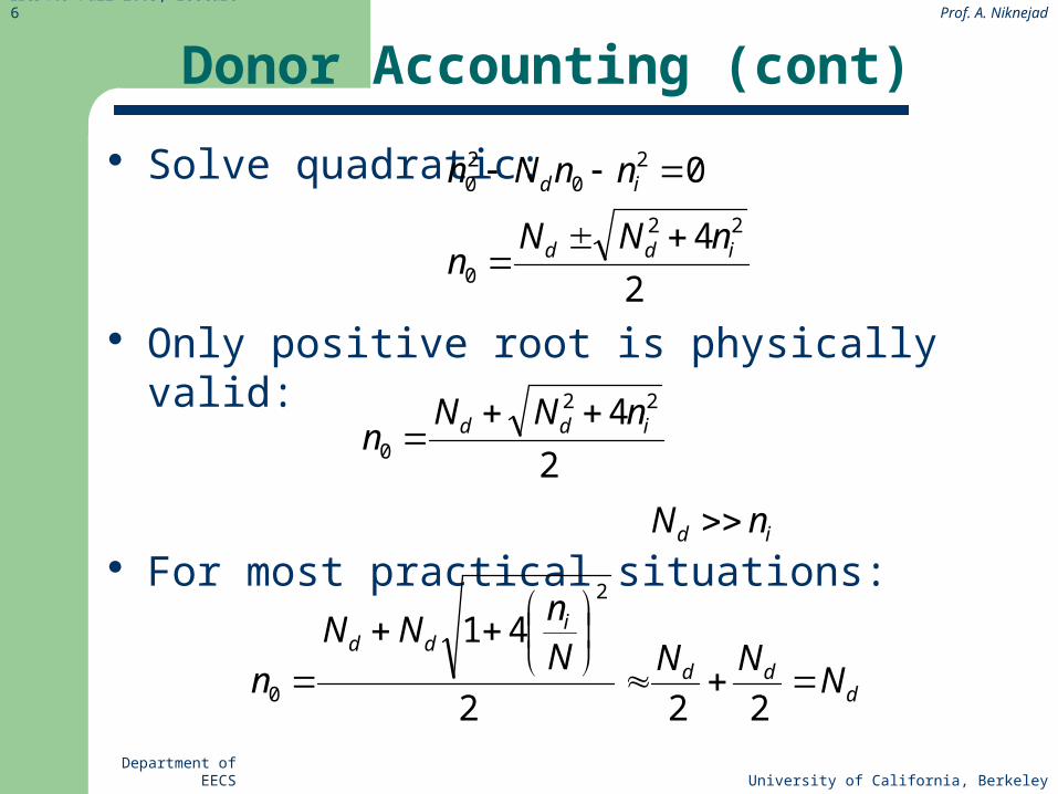
Donor Accounting (cont)
Solve quadratic:
Only positive root is physically valid:
For most practical situations:
2
4
0
22
0
20
20
idd
id
nNNn
nnNn
2
4 22
0idd nNN
n
id nN
ddd
idd
NNNN
nNN
n
222
412
0
Department of EECS University of California, Berkeley
EECS 105 Fall 2003, Lecture 6 Prof. A. Niknejad
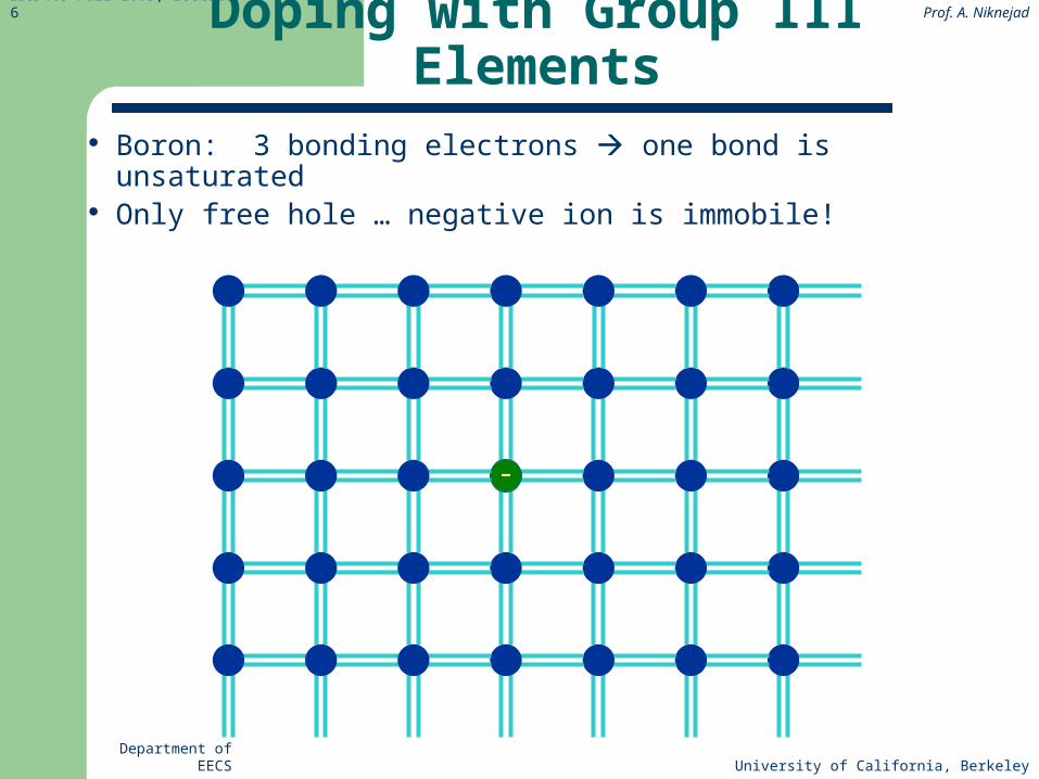
Doping with Group III Elements Boron: 3 bonding electrons one bond is unsaturated Only free hole … negative ion is immobile!
-
Department of EECS University of California, Berkeley
EECS 105 Fall 2003, Lecture 6 Prof. A. Niknejad
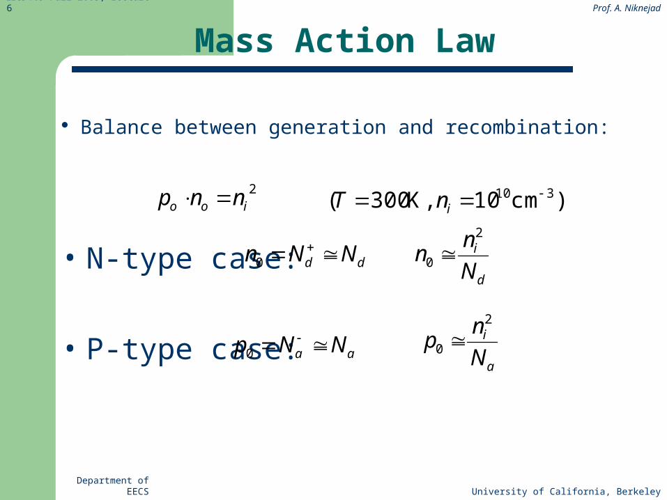
Mass Action Law
Balance between generation and recombination:
2ioo nnp
• N-type case:
• P-type case:
)cm10,K300( 310 inT
dd NNn 0
aa NNp 0
d
i
N
nn
2
0
a
i
N
np
2
0
Department of EECS University of California, Berkeley
EECS 105 Fall 2003, Lecture 6 Prof. A. Niknejad
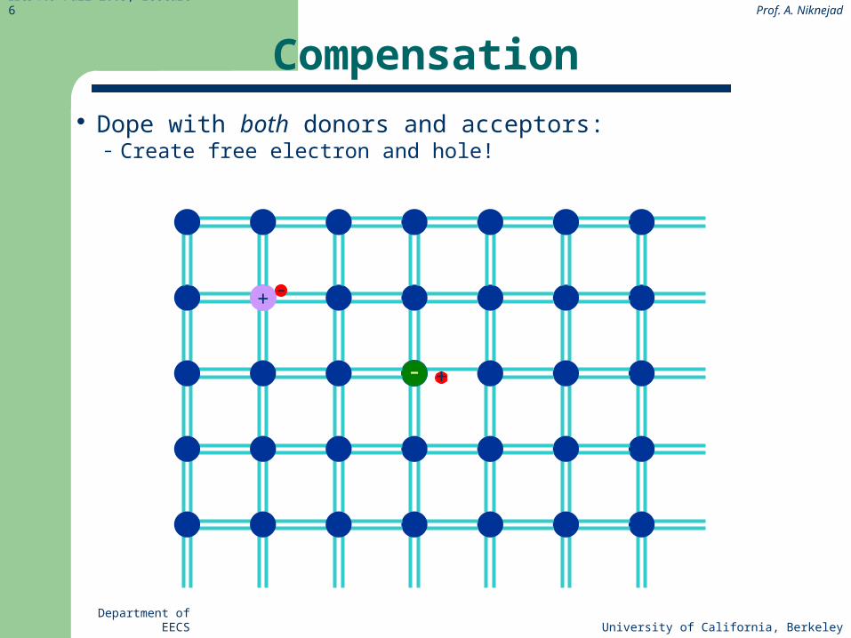
Compensation Dope with both donors and acceptors:
– Create free electron and hole!
+
-
-
+

Department of EECS University of California, Berkeley
EECS 105 Fall 2003, Lecture 6 Prof. A. Niknejad
Compensation (cont.)
More donors than acceptors: Nd > Na
iado nNNn
• More acceptors than donors: Na > Nd
ado NN
np i
2
idao nNNp da
o NN
nn i
2
Department of EECS University of California, Berkeley
EECS 105 Fall 2003, Lecture 6 Prof. A. Niknejad
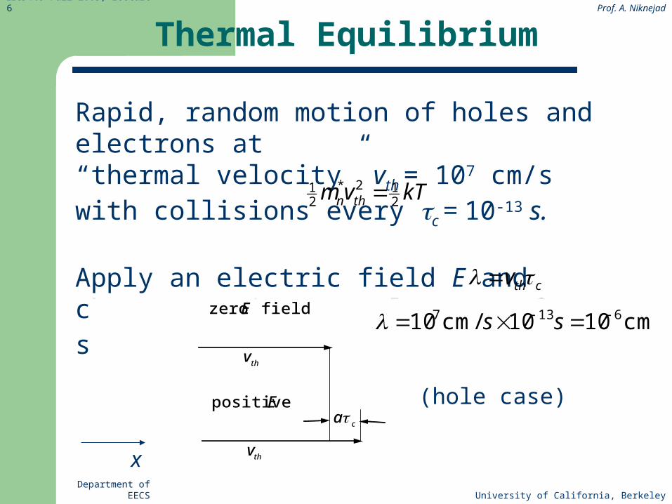
Thermal Equilibrium
Rapid, random motion of holes and electrons at “thermal velocity” vth = 107 cm/s with collisions every c = 10-13 s.
Apply an electric field E and charge carriers accelerate … for c seconds
zero E field
vth
positive E
vth
ac
(hole case)
x
kTvm thn 212*
21
cthv
cm1010/cm10 6137 ss
Department of EECS University of California, Berkeley
EECS 105 Fall 2003, Lecture 6 Prof. A. Niknejad
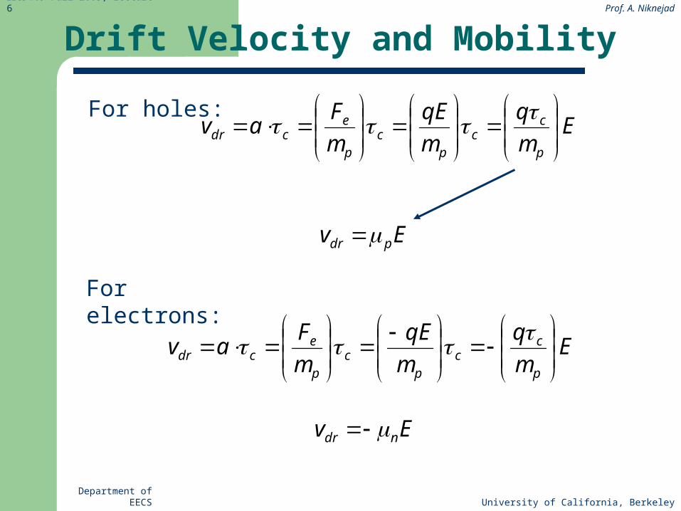
Drift Velocity and Mobility
Ev pdr
Em
q
m
qE
m
Fav
p
cc
pc
p
ecdr
For electrons:
Em
q
m
qE
m
Fav
p
cc
pc
p
ecdr
For holes:
Ev ndr
Department of EECS University of California, Berkeley
EECS 105 Fall 2003, Lecture 6 Prof. A. Niknejad
“default” values:
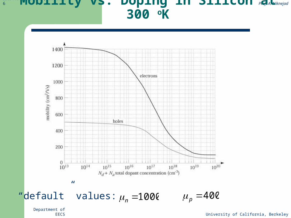
Mobility vs. Doping in Silicon at 300 oK
1000n 400p