lecture 8
TRANSCRIPT
Semiconductor Manufacturing and Processing

2
1950 1955 1960 1975 1980 1985 1990 1995 2000 2001 2002 2003 2004 2005 2006
2006
19523 Amp power Transistor
1960Si-Base Transistor
197916-Bit Processor MC68000
1975MC6800 is first microprocessor used in automotive application
198432-Bit Processor MC68020
1989MC68302 Communications Processor
Late 1980’sDevelopment of the first surface micromachined inertial sensors for the automotive airbag
1991PowerPC® (1) Alliance
1994First PowerPC® (1) MPC601
1991Company becomes leading supplier of automotive embedded processors
1998First PowerQUICC II communications processor (MPC8260)
2001MPC7455 SOI Volume Production
2003Low-K Volume Production
2003First single core modem: MXC. “Smartphone-on –a-postage stamp”
2003The pressure sensor portfolio expands with the tire pressure monitor sensor with capacitive technology to save power
200460 millionth applications processor for portable multimedia devices
2005First PowerQUICC communications processor with QUICC Engine (MPC8360E)
Building on a 50+ Year Heritage of Innovation
1995MPC860 PowerQUICC™
2005i.MX31 processor for mobile multimedia entertainment
2006MC9RS08KA2Ultra-low end MCU with RS08 core
2006MSC8144 multicore DSP targeting wireless and wireline infrastructure
2006Industry’s First Commercial MRAM
Product

Semiconductor Manufacturing In A Nutshell
3
1. Silicon
2. Wafer4. Product
3. Chip

Semiconductor Manufacturing Process Steps
4
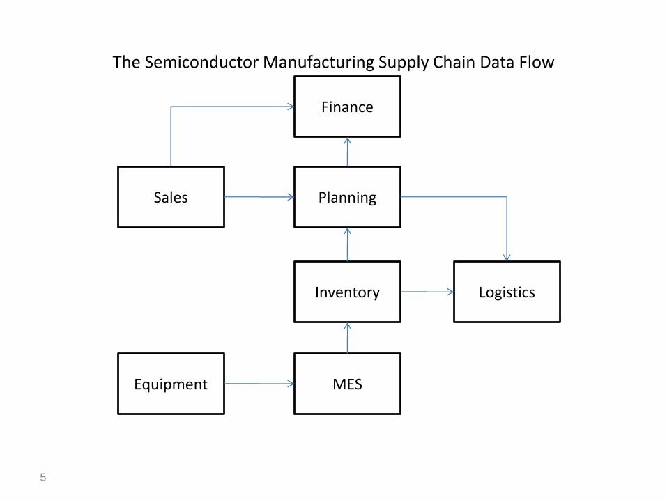
The Semiconductor Manufacturing Supply Chain Data Flow
5
Equipment MES
Inventory Logistics
PlanningSales
Finance
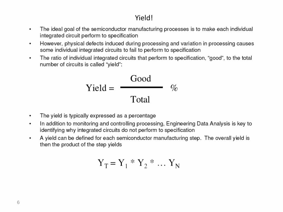
Yield!
6

Data Analysis for Yield Improvement – Wafer Maps
Single Wafer
Multiple Wafer
A single wafer map represents 100’s to 1,000’s of data points; a multiple wafer map can represent 1,000’s to 100,000’s of data points.
Very high performance graphical data visualization …

The IC Market• The semiconductor industry is approaching $300B/yr in sales
Transportation 8%
Consumer Electronics16%
Communications24%
Computers42%
Industrial8%
Military2%
Courtesy of Dr. Bill Flounders, UC Berkeley Microlab

IC Technology AdvancementImprovements in IC performance and cost have been enabled by the steady miniaturization of the transistor
Better Performance/Cost
Market Growth
2000 2005 2010 2015 20201
10
100
GA
TE
LE
NG
TH
(n
m)
YEAR
LOW POWER
HIGH PERFORMANCE
International Technology Roadmap for Semiconductors
Transistor Scaling
Investment
SMIC’s Fab 4 (Beijing, China)
Photo by L.R. Huang, DigiTimes
PITCH
YEAR: 2004 2007 2010 2013 2016
HALF-PITCH: 90nm 65nm 45nm 32nm 22nm

The Nanometer Size Scale
Carbon nanotube
MOSFET

• Goal: Mass fabrication (i.e. simultaneous fabrication) of many IC “chips” on each wafer, each containing millions or billions of transistors
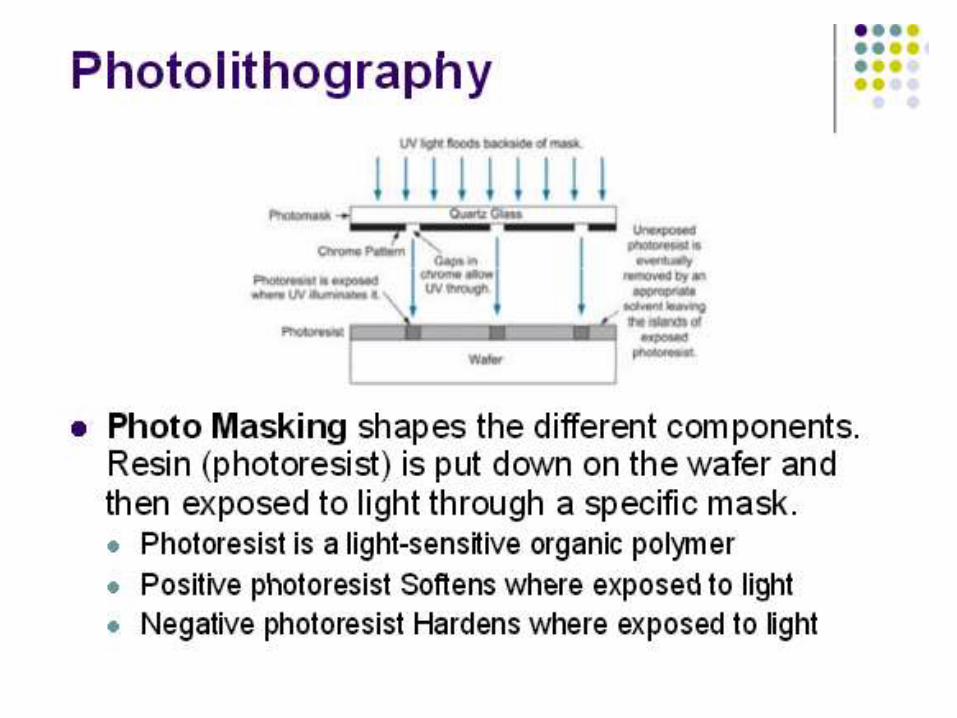
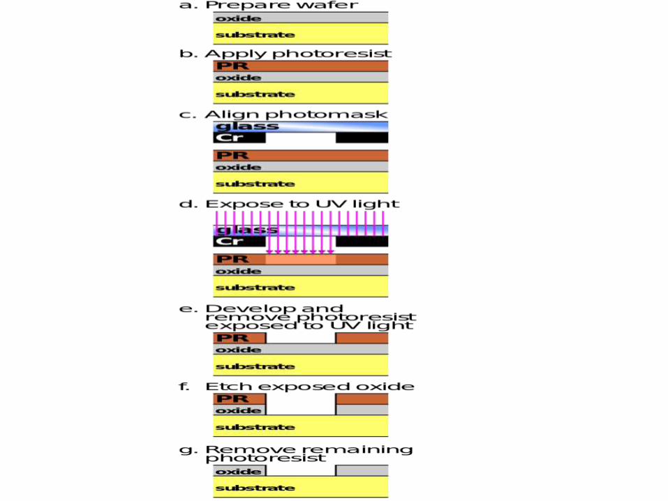
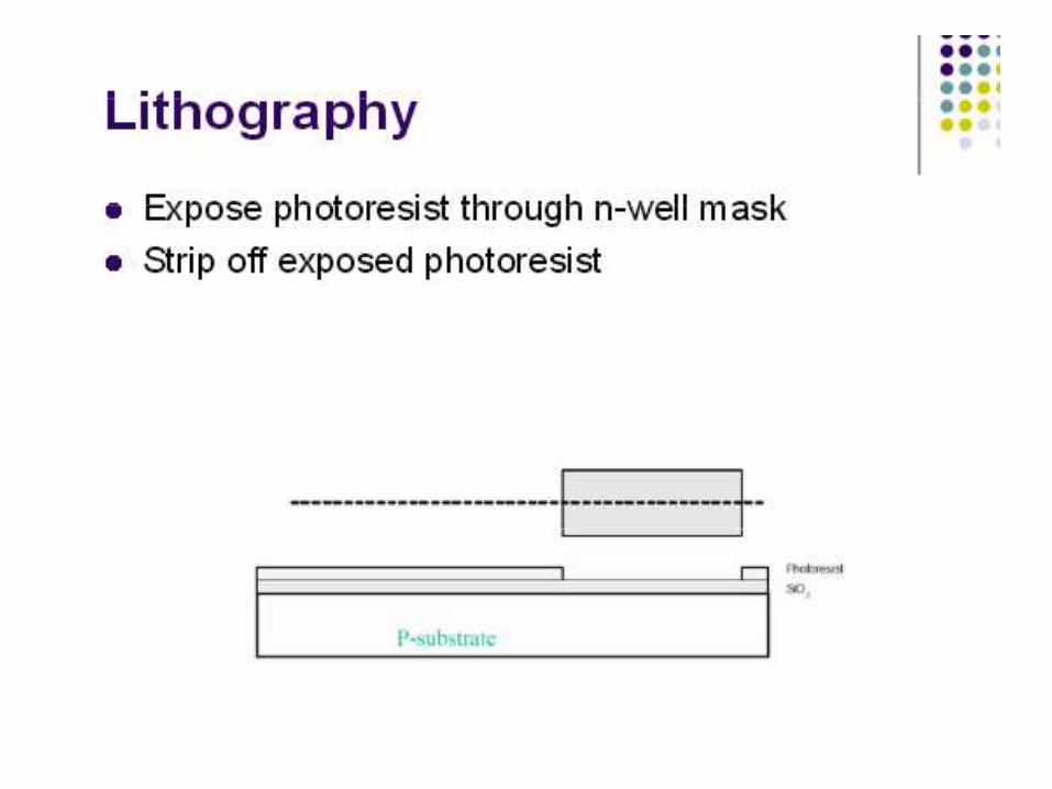
• Approach: Form thin films of semiconductors, metals, and insulators over an entire wafer, and pattern each layer with a process much like printing (lithography).
IC Fabrication
Planar processing consists of a sequence of additive and subtractive steps with lateral patterning
oxidation
deposition
ion implantation
etching lithography

• DEPOSITION of a thin film
• LITHOGRAPHY– Coat with a protective layer– Selectively expose the protective layer– Develop the protective layer
• ETCH to selectively remove the thin film
• Strip (etch) the protective layer
Planar Processing(patented by Fairchild Semiconductor in 1959: J. A. Hoerni, US Patent 3,064,167)
Courtesy of Dr. Bill Flounders, UC Berkeley Microlab

Deposition/growth
Etch
Epitaxy
Anneal
CMP
Ion Implantation
Test
CD SEMMetrology
DefectDetection
Lithography
Mask Pattern Generation
Bare SiliconWafer
ProcessedWafer
Overview of IC Process Steps
Courtesy of Dr. Bill Flounders, UC Berkeley Microlab

G
S D
Si classical
multi-gateG
S DSi
G
high-k gate dielectric
metallic gate
strained Si
Lg (nm): 50 40 30 20 10
MOSFET Scaling Scenario• Advanced structures will enable Si MOSFET scaling to Lg <10 nm
forward body biasing
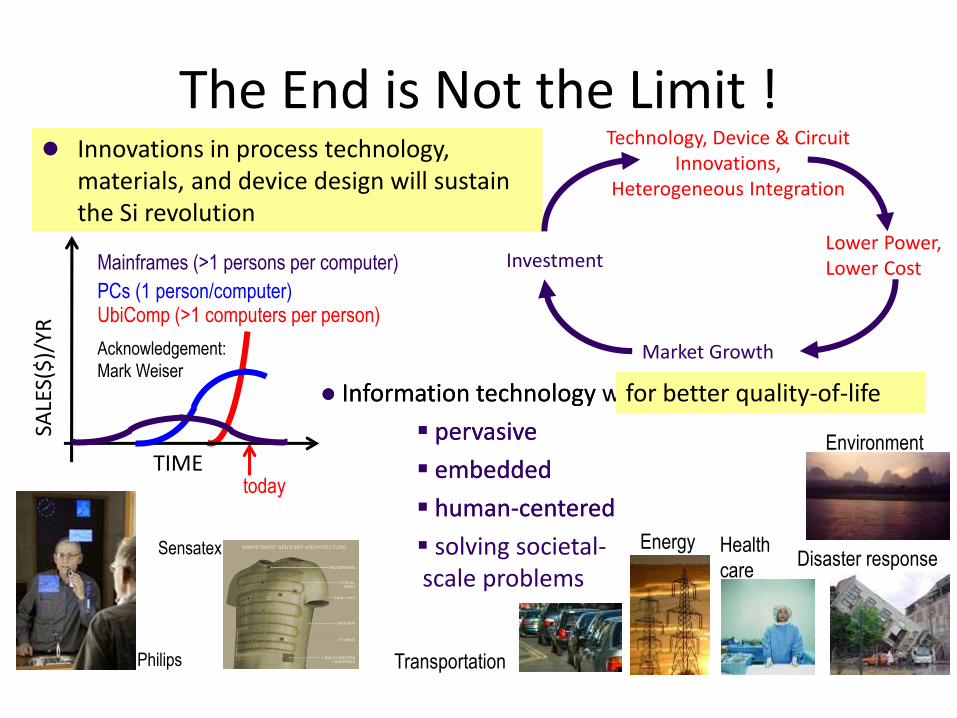
The End is Not the Limit !
Information technology
pervasive
embedded
human-centered
solving societal-scale problems
Philips
Innovations in process technology, materials, and device design will sustain the Si revolution
Lower Power,Lower Cost
Market Growth
Technology, Device & CircuitInnovations,
Heterogeneous Integration
Investment
Acknowledgement:
Mark Weiser
UbiComp (>1 computers per person)
today
SALE
S($
)/YR
TIME
PCs (1 person/computer)
Mainframes (>1 persons per computer)
Transportation
Health
careDisaster response
Energy
Environment
Sensatex
Information technology will be
pervasive
embedded
human-centered
for better quality-of-life