lectures 5-8, page 1 engineering iia, 3b3 switch-mode ...prp/3b3/3b3lec5-8.pdf · simple to use,...
TRANSCRIPT

5 Thyristor Circuits I
5.1 The Thyristor
The thyristor was initially called a silicon controlled rectifier SCR as it has thediode-like property that it conducts in one direction only but with the importantdifference that the onset of conduction could be controlled. The ability tocontrol a rectifier made economical the widespread use of variable voltage ac-dc‘converter’ circuits. The need for such ‘controlled rectification’ at high voltageand high current is undiminished and the thyristor remains attractive. It issimple to use, electrically robust and single units are available with high ratings(e.g. 3000A, 4.5kV).
5.1.1 Thyristor characteristic
With a forward voltage applied, (the anode positive with respect to the cathode),the transition from blocking to conducting occurs when a small positive voltageis applied to the gate. When conducting the device has a forward drop of about 2 V over a wide current range.
A thyristor will not remain conducting after the removal of a gate pulseunless the forward current is above a minimum value, the latching current,about 40 mA for most devices (even big ones). Similarly conduction willstop if the forward current falls below a certain level, the holding current.
Lectures 5-8, Page 1 Engineering IIA, 3B3 Switch-Mode Electronics

If an excessive reverse voltage is applied, the thyristor breaks down and isdestroyed.
If an excessive forward voltage is applied, breakover occurs and the devicebecomes conducting. Although breakover is not necessarily destructive, it is nota recommended mode of operation (except for small ‘diacs’).
A recovery time, typically 25-200µs, is needed after forward conductionbefore forward volts can be sustained. During this time, carriers in thedevice to recombine. The rate of re-application of forward voltage is limited.
5.1.2 Thyristor construction
The thyristor is a four layer device, p-n-p-n.
The forward voltage is blocked by the N1 - P2 junction and the reverse voltageby the N1 - P1 junction.
The operation can be understood by considering the coupled npn and pnptransistors. When the npn device is turned on by the gate pulse, it supplies thebase current of the pnp, which in turn supplies the base current of the npn,enabling the external drive to the gate to be removed.
The current gains of the two transistors are low and they vary with current.Consequently, at a low forward current the base currents are inadequate tomaintain conduction - this is the origin of the holding and latching currents.
Lectures 5-8, Page 2 Engineering IIA, 3B3 Switch-Mode Electronics
5.2 The control of dc power
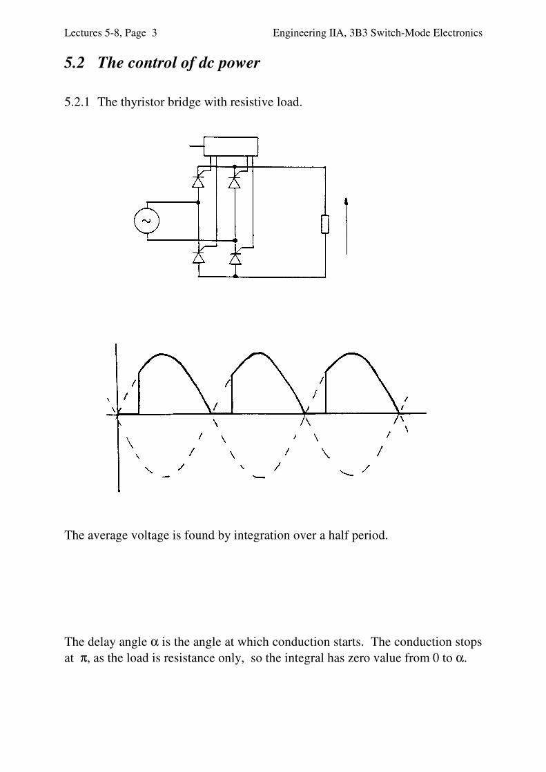
5.2.1 The thyristor bridge with resistive load.
The average voltage is found by integration over a half period.
The delay angle α is the angle at which conduction starts. The conduction stopsat π, as the load is resistance only, so the integral has zero value from 0 to α.
Lectures 5-8, Page 3 Engineering IIA, 3B3 Switch-Mode Electronics

Hence, the dc output voltage is adjustable.
As expected, the average voltage depends on α , the delay angle. Settingα=0, the output becomes a series of complete half sine waves, as in the
bridge rectifier, and the output voltage is then , as found earlier for2 2 V�
the diode bridge.
5.2.2 Load with resistance and inductance, and continuous current
Inductance may be present in the load, as in a dc motor, or may be added forsmoothing, as described in Lecture 3.
Waveforms:
Lectures 5-8, Page 4 Engineering IIA, 3B3 Switch-Mode Electronics
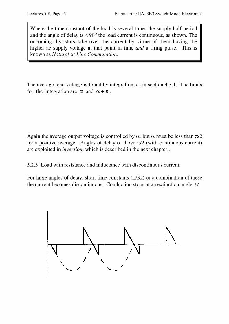
Where the time constant of the load is several times the supply half periodand the angle of delay α < 90O the load current is continuous, as shown. Theoncoming thyristors take over the current by virtue of them having thehigher ac supply voltage at that point in time and a firing pulse. This isknown as Natural or Line Commutation.
The average load voltage is found by integration, as in section 4.3.1. The limitsfor the integration are α and α + π .
Again the average output voltage is controlled by α, but α must be less than π/2for a positive average. Angles of delay α above π/2 (with continuous current)are exploited in inversion, which is described in the next chapter..
5.2.3 Load with resistance and inductance with discontinuous current.
For large angles of delay, short time constants (L/RL) or a combination of thesethe current becomes discontinuous. Conduction stops at an extinction angle ψ.
Lectures 5-8, Page 5 Engineering IIA, 3B3 Switch-Mode Electronics

As usual, the average output voltage is found by integration. The limits ofintegration are , α and ψ.
The angle ψ is found from the differential equation for current
solving for the angle ψ at which i = 0 The Maths is not pleasant (orexaminable!).
5.3 The control of ac power
5.3.1 Back to Back thryristors
The use of two thyristors in inverse parallel permits the control of ac power.Two gate drive circuits are needed.
Lectures 5-8, Page 6 Engineering IIA, 3B3 Switch-Mode Electronics
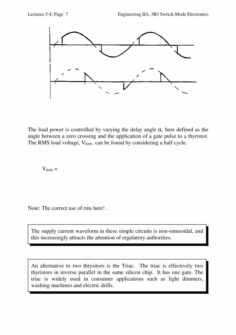
The load power is controlled by varying the delay angle α, here defined as theangle between a zero crossing and the application of a gate pulse to a thyristor.The RMS load voltage, VRMS , can be found by considering a half cycle.
VRMS =
Note: The correct use of rms here! .
The supply current waveform in these simple circuits is non-sinusoidal, andthis increasingly attracts the attention of regulatory authorities.
An alternative to two thrysitors is the Triac. The triac is effectively twothyristors in inverse parallel in the same silicon chip. It has one gate. Thetriac is widely used in consumer applications such as light dimmers,washing machines and electric drills.
Lectures 5-8, Page 7 Engineering IIA, 3B3 Switch-Mode Electronics
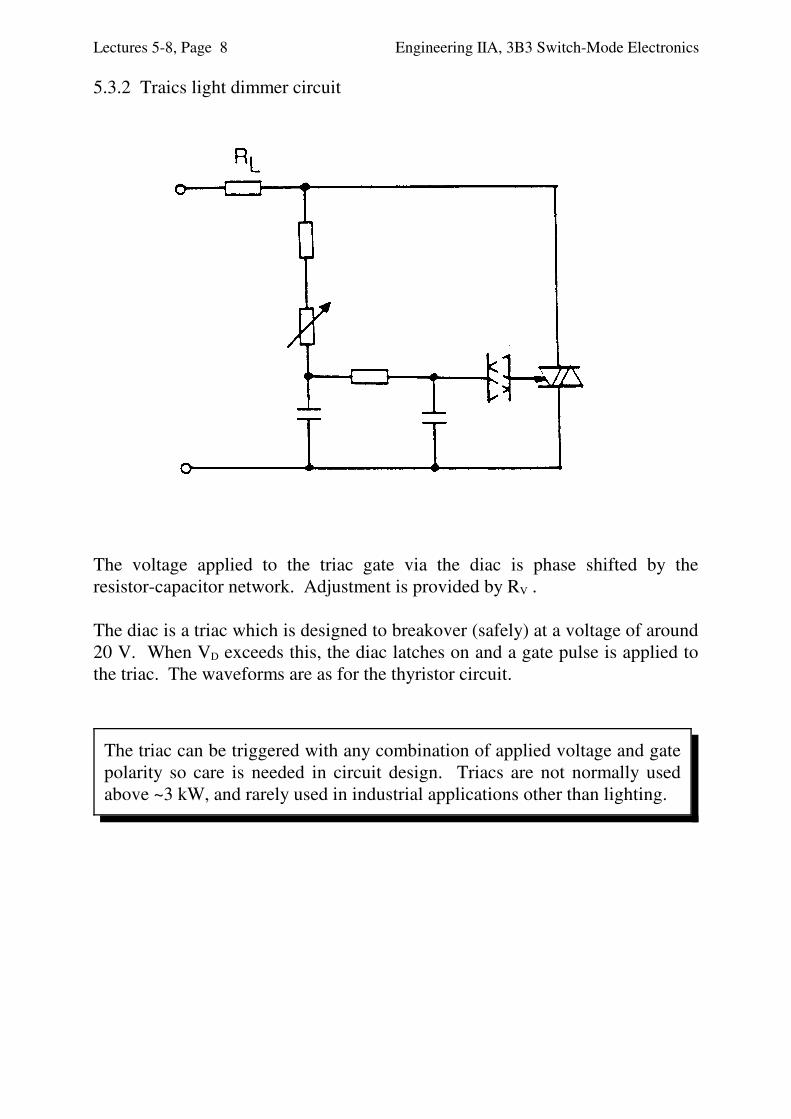
5.3.2 Traics light dimmer circuit
The voltage applied to the triac gate via the diac is phase shifted by theresistor-capacitor network. Adjustment is provided by RV .
The diac is a triac which is designed to breakover (safely) at a voltage of around20 V. When VD exceeds this, the diac latches on and a gate pulse is applied tothe triac. The waveforms are as for the thyristor circuit.
The triac can be triggered with any combination of applied voltage and gatepolarity so care is needed in circuit design. Triacs are not normally usedabove ~3 kW, and rarely used in industrial applications other than lighting.
Lectures 5-8, Page 8 Engineering IIA, 3B3 Switch-Mode Electronics
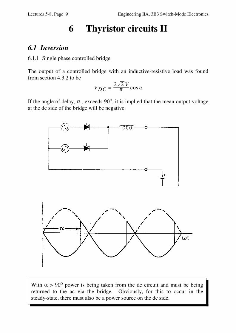
6 Thyristor circuits II
6.1 Inversion6.1.1 Single phase controlled bridge
The output of a controlled bridge with an inductive-resistive load was foundfrom section 4.3.2 to be
V DC = 2 2 V� cos �
If the angle of delay, α , exceeds 90O, it is implied that the mean output voltageat the dc side of the bridge will be negative.
With α > 90O power is being taken from the dc circuit and must be beingreturned to the ac via the bridge. Obviously, for this to occur in thesteady-state, there must also be a power source on the dc side.
Lectures 5-8, Page 9 Engineering IIA, 3B3 Switch-Mode Electronics

This mode of operation, converting dc to ac, is known as inversion. A circuitwhich can act as both a rectifier and inverter, is known as a converter.
In principle the delay angle can be increased to 180O, but thyristors need aminimum recovery time before voltage can be re-applied, as mentioned insection 5.1.1.
6.1.2 Three-phase bridge converters
In practice, the use of thyristor converters is largely confined to three-phasesystems at high powers. The three-phase controlled bridge is similar to thethree-phase bridge rectifier.
Waveforms for a delay angle α = 45O , with all voltages with respect to thesupply star point.
Note the origin for the delay angle α .
Lectures 5-8, Page 10 Engineering IIA, 3B3 Switch-Mode Electronics
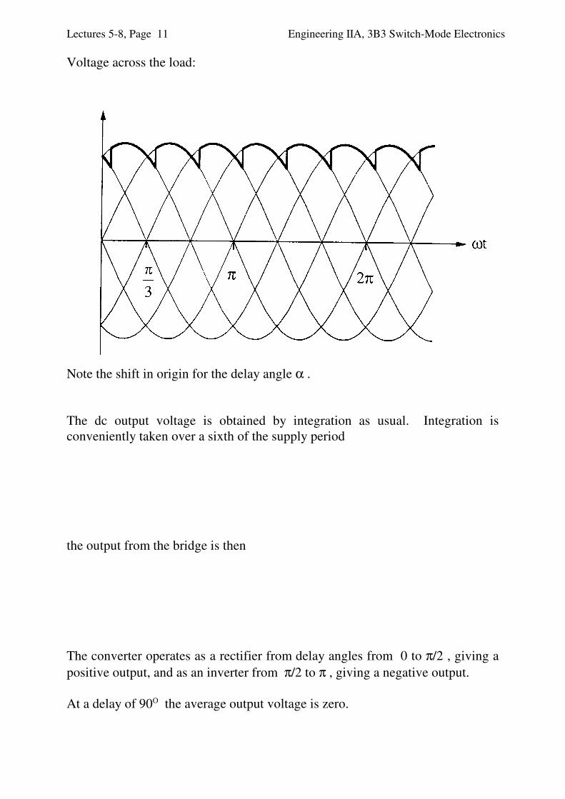
Voltage across the load:
Note the shift in origin for the delay angle α .
The dc output voltage is obtained by integration as usual. Integration isconveniently taken over a sixth of the supply period
the output from the bridge is then
The converter operates as a rectifier from delay angles from 0 to π/2 , giving apositive output, and as an inverter from π/2 to π , giving a negative output.
At a delay of 90O the average output voltage is zero.
Lectures 5-8, Page 11 Engineering IIA, 3B3 Switch-Mode Electronics
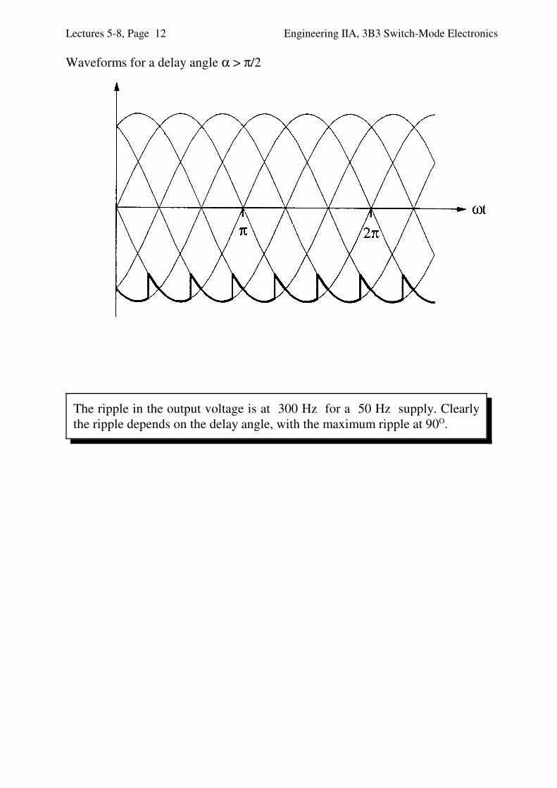
Waveforms for a delay angle α > π/2
The ripple in the output voltage is at 300 Hz for a 50 Hz supply. Clearlythe ripple depends on the delay angle, with the maximum ripple at 90O.
Lectures 5-8, Page 12 Engineering IIA, 3B3 Switch-Mode Electronics

6.2 Thyristor commutation in converters
6.2.1 Angle of overlap in converters
The ac supply, especially if derived from a transformer, can contain significantleakage reactance.
Starting with T1 on: Thyristor T2 is triggered when its supply voltage is higherthan that of T1 , therefore the current prefers the new path through T2 .
However, the series inductance limits the rate of change of the current, so T1 andT2 are on together for a short time and the difference in their supply voltagesforces the current to transfer.
For small angles of overlap, the current transition can be approximated by alinear di/dt. Note the start and end conditions.
The angle of overlap will be a function of the current to be commutated and thedelay angle α , which sets the initial difference in the voltage of the two phases( V1 - V2 = 0 at α = 0 ).
Lectures 5-8, Page 13 Engineering IIA, 3B3 Switch-Mode Electronics

Analysis:
The output voltage VO will have a notch in it, which corresponds to theoverlap time µ and results form the potential divider action of the two phaseinductances, making the output the average of the two instantaneousvoltages for the overlap time.
As the ‘lost’voltage is proportional to the output current, it appears as if there isa resistance in series with the output of the bridge. For the circuit above theresistance has the value
6.2.2 Commutation Failure
Clearly the anode current in the thyristor being commutated falls to zero at theend of the overlap time. The thyristor cannot support any forward volts untilafter the recovery time, tq as described in Section 5. Converter grade thyristorsrecover in about 200 µs.
Commutation failure occurs when forward volts are reapplied to the thyristorbeing commutated before the whole process is complete. This is only a problemat the extreme range of delay α , near 180O.
Commutation failure in inversion may have alarming effects, since theconverter suddenly produces a half cycle of positive voltage!
Lectures 5-8, Page 14 Engineering IIA, 3B3 Switch-Mode Electronics

6.3 Further thyristor applications
If thyristors are to be used with dc supplies natural commutation is not possible.
6.3.1 Load resonant commutation
The least complicated way of using thyristors in dc circuits is to resonate theload such that the current in the thyristors returns to zero following a half cycleof resonance. This will be dealt with in a later lecture under ‘resonantconverters’.
6.3.2 * Forced commutation
Only found in historic equipment - Not examinable.
6.4 The gate turn-off thyristor (GTO)
Recall that the thyristor is a four terminal device and can be thought of as twocoupled transistors.
If the base current of the npn transistor can be diverted, it can be turned off andthe whole device turned off. The thyristor must be specifically designed for thismode of use and as a result they are usually referred to as ‘GTOs’ or ‘IGCTs’.
Although the concept of the gate turn-off thyristor has been known since thediscovery of the thyristor, practical devices only emerged in the 1990s.Such devices are confined to high currents and voltages, where the lowthyristor on-state voltage ~2V is very attractive.
Lectures 5-8, Page 15 Engineering IIA, 3B3 Switch-Mode Electronics

6.4.1 Snubber circuits*
To avoid unwanted latchup, thyristors are always protected by a ‘snubber’consisting of a small inductance in series and a small capacitor resistorcombination in parallel. This filters out high dv/dt ‘s so that capacitive currentsthrough the thyristor are small and do not cause unwanted latch-up.
* Not in exam
Lectures 5-8, Page 16 Engineering IIA, 3B3 Switch-Mode Electronics

7 MOSFET transistors as switches
Transistors are attractive as switches as they can be easily turned on and turnedoff, unlike thyristors. The bipolar transistor was the earliest device, followed bypractical power MOSFETs and most recently by insulated gate bipolartransistors, IGBTs. Each device has its own characteristic and no one devicehas ideal properties. The advance of MOSFET device ratings has led to theirapplication to power levels up to tens of kW.
7.1 Introduction to the power MOSFET
The field effect transistor exists in several variants but most power MOSFETsare n-channel enhancement mode devices. The current flow, which is controlledby the gate voltage, only involves electrons. The MOSFET can be made as alateral device, as in normal integrated circuit technology, or as a vertical device.MOSFETs have two advantageous features as switches. The resistive nature ofthe channel causes sharing of the drain current, avoiding hot-spots in the device,and the capacitor like gate simplifies gate drive arrangements, having a highimpedance at dc and moderate frequencies. Single devices rated at up to 1000 Vand 50 A available.
7.1.1* Construction of MOSFETs
The lateral power MOSFET:
Lateral devices, as used in power integrated circuits, are easily fabricatedand devices on the same chip can be mutually isolated by forming them inan SiO2 ‘bucket’. However, the silicon area is not well utilised for highvoltage devices as a significant lateral distance drain to source is needed towithstand high voltages.
* Not in exam.
Lectures 5-8, Page 17 Engineering IIA, 3B3 Switch-Mode Electronics

The vertical power MOSFET:
The voltage rating still requires a significant distance drain to source, butthis distance is now formed vertically. The surface area of the chip is thenused efficiently. Low doping in the drain extends the depletion layer in thedrain side, as for the equivalent p-n diode. The current rating is increasedby paralleling more cells until the area of silicon becomes limited byfabrication difficulties. Such paralleling is permissible as MOSFETs sharecurrent well.
7.1.2 Operation of MOSFETs
Consider a lateral n-channel device as an example. The silicon under the gate isp-type, so diodes are formed between this region and the n+ source and the n-drain. With the drain biased positive with respect to the source, diode at thedrain is reverse biased and no current can flow.
Making the gate positive with respect to the source, the gate becomes charged inthe manner of a capacitor and electrons in the p-type are attracted to form a thinlayer under the gate. This conducting channel is called the inversion layer.
Lectures 5-8, Page 18 Engineering IIA, 3B3 Switch-Mode Electronics

The channel appears n-type, hence the device is known as an n-channelMOSFET. Drain current can flow if the drain is made positive with respectto the source. Current flow consists of electrons. The threshold voltage, VT
, is the minimum gate-source voltage required to create a channel.
7.1.3 I-V characteristics of MOSFETs
When VDS is high, that is VDS > VGS - VT, the device is said to be saturated. Inthis condition the high drain voltage causes the channel to narrow or pinch off,at the drain. As a result the drain current, ID , is practically independent of VDS
and depends only on VG. In this region, which is used by class AB amplifiercircuits, it can be shown that
At low values of VDS, VDS < VGS - VT, the device is said to be in the linearregion. In this region the channel appears resistive as the drain current isproportional to the drain voltage. The on-resistance of the device, RDSon, isdefined for a high value of VGS, so the on-state voltage is
VDS = ID RDSon
RDSon is given by the channel resistance in series with the drain resistanceand is specified at a particular gate-source voltage and 25OC.
Lectures 5-8, Page 19 Engineering IIA, 3B3 Switch-Mode Electronics
Although p-channel MOSFETs are made, for a device of equal dimensionsthe RDSon will be about three times greater than the equivalent n-channelMOSFET. Hence, p-channel MOSFETs are usually avoided in switchedmode circuits.
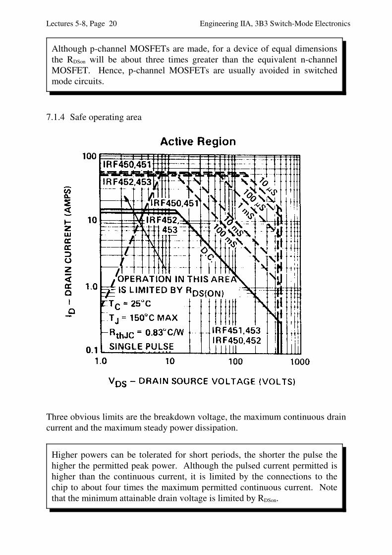
7.1.4 Safe operating area
Three obvious limits are the breakdown voltage, the maximum continuous draincurrent and the maximum steady power dissipation.
Higher powers can be tolerated for short periods, the shorter the pulse thehigher the permitted peak power. Although the pulsed current permitted ishigher than the continuous current, it is limited by the connections to thechip to about four times the maximum permitted continuous current. Notethat the minimum attainable drain voltage is limited by RDSon.
Lectures 5-8, Page 20 Engineering IIA, 3B3 Switch-Mode Electronics

7.2 MOSFET switching behaviour
7.2.1 The inverse parallel Diode
The drain (n), channel (p) and source (n) form an npn bipolar transistor. Thebase is shorted to the emitter to stop any bipolar transistor action. Thiseffectively makes a diode in inverse parallel across the MOSFET.
In modern power MOSFETs, this diode is optimised to be a ‘fast’ diode sothat it can be used if desired.
7.2.2 Device capacitances
CGD, called the Miller capacitance, depends on VGD; CDS is also the capacitanceof a depletion layer so varies with VDS. CGS is the capacitance of the gate tosource and is essentially constant.
Lectures 5-8, Page 21 Engineering IIA, 3B3 Switch-Mode Electronics

On data sheets, the input capacitance Ciss, the output capacitance Coss and thereverse transfer capacitance Crss are quoted. The are obtained from simple tests.The relationships with the capacitances shown are:
As these capacitances vary with voltage, manufacturers often state the totalcharge required at the input for a given drain-source voltage change.
7.2.3 Turn on with a freewheeling inductive load
Assume the load has a high inductance so the load current is essentiallyconstant. The freewheel diode carries the load current when the transistor is off.This is a common situation in switching circuits.
Suppose a step input is applied to the gate circuit. The gate voltage will rise asthe gate capacitance is charged through RG. The turn-on can be divided intofour periods as shown in the waveforms of drain voltage, drain current and gatevoltage.
Lectures 5-8, Page 22 Engineering IIA, 3B3 Switch-Mode Electronics

Period I - The MOSFET is off
In this period, the MOSFET is off. VGS rises until VT is reached, when period IIstarts. The gate voltage is of the form
VT is usually 2 - 4 V.
Period II - The MOSFET turns on
The MOSFET turns on and the drain current rises.
At a gate voltage of VGS2 the MOSFET is carrying the whole load current.
Period III - The MOSFET is carrying the load current
Once the MOSFET is carrying the load current, the drain voltage falls and acurrent flows into the gate through CGD opposing the rise in gate voltage. Thegate voltage remains at VGS2.
Period IV - The MOSFET enters the final on state
The MOSFET enters its linear region as VDS becomes less than VGS - VT. Thegate voltage rises asymptotically to V, and the drain voltage falls to RDSon ID
(provided VGG is large enough)
The rise and fall times are set by circuit capacitances and the gate driveresistance. In the on-state, the voltage across the MOSFET is ID.RDSon
provided VGS is large enough. The device is off if VGS < VT.
Lectures 5-8, Page 23 Engineering IIA, 3B3 Switch-Mode Electronics

7.3 Gate drive circuits
Virtually no steady gate current (< 1nA), is needed, but for fast switchingspeeds substantial currents, 1A or more, are needed to charge and dischargeCiSS. In general a low impedance gate drive is needed.
Circuit 1 - direct drive from CMOS
This circuit is simple but slow as the current drive capability of the CMOS gatesis limited. Gates can be paralleled for greater speed.
Circuit 2 - a drive using discrete devices
The current drive capacity is increased by using a complementary emitterfollower.
Lectures 5-8, Page 24 Engineering IIA, 3B3 Switch-Mode Electronics
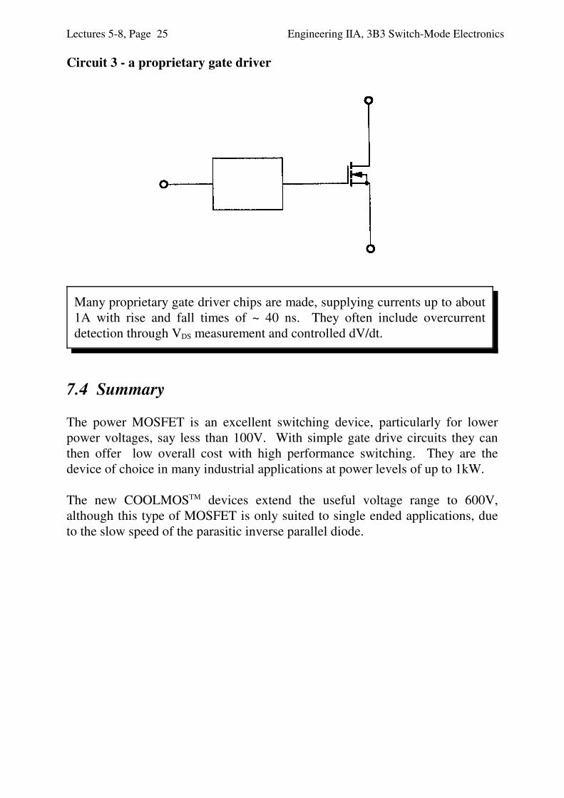
Circuit 3 - a proprietary gate driver
Many proprietary gate driver chips are made, supplying currents up to about1A with rise and fall times of ~ 40 ns. They often include overcurrentdetection through VDS measurement and controlled dV/dt.
7.4 Summary
The power MOSFET is an excellent switching device, particularly for lowerpower voltages, say less than 100V. With simple gate drive circuits they canthen offer low overall cost with high performance switching. They are thedevice of choice in many industrial applications at power levels of up to 1kW.
The new COOLMOSTM devices extend the useful voltage range to 600V,although this type of MOSFET is only suited to single ended applications, dueto the slow speed of the parasitic inverse parallel diode.
Lectures 5-8, Page 25 Engineering IIA, 3B3 Switch-Mode Electronics

8 Bipolar Transistor Switching DevicesThe MOSFET is easy to drive and can switch at a high speed. However, toachieve a low voltage drop in the on-state, RDSon must be made small and thisneeds large devices, which may be expensive.
In contrast, the bipolar transistor has an on-state drop which is nearlyindependent of load current, although a large base current is required for the onstate. A modern compromise is the insulated gate bipolar transistor, IGBT,which for high voltage devices combines the ease of control of a MOSFET withthe low forward drop of a Bipolar transistor.
8.1 The bipolar transistor as a switch8.1.1 * The construction of power bipolar transistors
The vertical power Bipolar Transistor:
* Not in examThe depletion layer for a high breakdown voltage is accommodated in the lowdoped collector region shown, but the base doping, base thickness or both needto be increased to prevent the depletion region of the collector-base junctionfrom punching through the base to the emitter.
As with MOSFETs, bipolar transistors can be lateral devices, as inintegrated circuits, or vertical devices, which make better use of silicon area.Power Bipolar transistors are usually a highly convoluted single devicestructures as current is not easily shared in bipolar devices.
Lectures 5-8, Page 26 Engineering IIA, 3B3 Switch-Mode Electronics

8.1.2 I-V characteristics and saturation
8.1.3 ‘Forced’ current gain
In the on state, the current flows in the transistors as shown.
For a low on-state voltage the wide n- collector region and the base must befilled up with stored charge, which means a large amount of recombinationwill happen and thus a high base current is required for equilibrium.
Lectures 5-8, Page 27 Engineering IIA, 3B3 Switch-Mode Electronics

8.1.4 Measured characteristics
Operating with a forced gain of 10 or less still represents a high power gainas the base drive is drawn from a low voltage. The correct operation of theBipolar Transistor is heavily dependent on the base drive conditions.
8.1.5 Safe operating area
As with MOSFETS, higher powers can be tolerated for short periods, but at highcollector emitter voltages second breakdown creates local hot spots generateextra carriers, allowing more current to crowd into those regions, an effect thatultimately causes the destruction of the device. (See above - A highertemperature gives a higher gain).
Bipolar transistors are usually found in high volume applications such asCompact Fluorescent Lamps, where their operation is tightly constrainedand the base drive and overall performance can be nicely optimised.
Lectures 5-8, Page 28 Engineering IIA, 3B3 Switch-Mode Electronics

In the on state, there is a maximum permitted steady collector current (1), amaximum collector emitter voltage (4) and maximum steady power (2). Thepower dissipation is reduced at high collector emitter voltages by a phenomenonknown as second breakdown (3).
The switching performance is often for a specific circuit, such as the CFLamp.
8.2 Switching the bipolar transistor8.2.1 Base drive considerations
The base current is high in the on state, so any base drive circuit must have alow output resistance. This is most easily obtained using a complementaryemitter follower circuit, as for the MOSFET. As the reverse breakdown voltageof the base emitter junction, usually about 8 V, the negative voltage rail mustnot exceed about 6V.
Lectures 5-8, Page 29 Engineering IIA, 3B3 Switch-Mode Electronics

The Baker's clamp or ‘antisaturation clamp’:
This circuit is often included to reduce the depth of saturation in the onstate. While full saturation reduces the voltage drop, the turn off becomesslow and lossy.
8.3 The power Darlington
Darlington connected power transistors are available, usually made on onepiece of silicon, including the resistors shown. Often slow switching.
Lectures 5-8, Page 30 Engineering IIA, 3B3 Switch-Mode Electronics

8.4 The insulated gate bipolar transistor, IGBT8.4.1* Construction of the IGBT
The desire to combine the ease of drive of the MOSFET and the low on-statedrop of the bipolar transistor has led to the development of the IGBT, whichessentially uses a MOSFET to control the base current of a large BiploarTransistor (a bit like a Darlington).
Vertical IGBT:
Note the labeled ‘collector’ is actually the emitter of the internal pnp!
The MOSFET supplies the base current of the pnp power transistor;
1. Recombination
2. Electron current lost
The on-state drop is typically around 2-4 V. The current handling andvoltage blocking capacity is very high (upto 2000A, 4.5kV) but the turn offmaybe slow with the trade off of a lower on-state voltage. Applications areindustrial motor drives, trains and ships.
Lectures 5-8, Page 31 Engineering IIA, 3B3 Switch-Mode Electronics
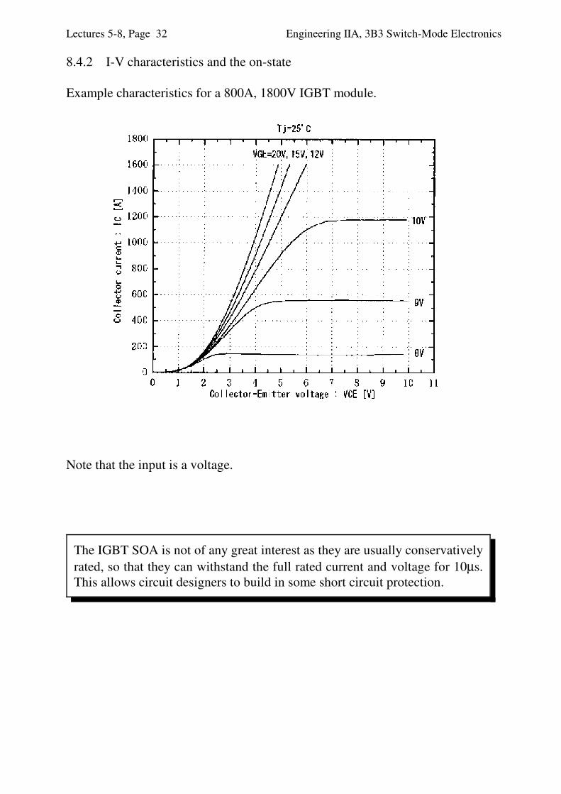
8.4.2 I-V characteristics and the on-state
Example characteristics for a 800A, 1800V IGBT module.
Note that the input is a voltage.
The IGBT SOA is not of any great interest as they are usually conservativelyrated, so that they can withstand the full rated current and voltage for 10µs.This allows circuit designers to build in some short circuit protection.
Lectures 5-8, Page 32 Engineering IIA, 3B3 Switch-Mode Electronics

8.5 The IGBT as a switch
When switching a large IGBT, a gate current of about 1A or more is necessaryto achieve reasonably rapid switching.
The turn on switching waveforms for IGBTs are very similar to those drawnfor the MOSFET in class. However, high voltage devices take a long timeto settle into their final on-state as the bipolar base charge has to build up.
Example waveforms, Turn Off:
At turn off, the trapped charge in the bipolar part of the IGBT allows somecurrent to keep flowing for a little while after turn off. This is known as the‘current tail’. While the current tail is insignificant in appearance, it shouldbe remembered that the IGBT is almost off and the voltage VCE across it ishigh, so the power lost in the IGBT is then quite high. Note also the delay atturn off.
P. R. PalmerOctober, 2008
Lectures 5-8, Page 33 Engineering IIA, 3B3 Switch-Mode Electronics