lessons in electric circuits, volume iii --...
TRANSCRIPT

Fifth Edition, last update January 18, 2006

2

Lessons In Electric Circuits, Volume III – Semiconductors
By Tony R. Kuphaldt
Fourth Edition, last update January 18, 2006

i
c©2000-2006, Tony R. Kuphaldt
This book is published under the terms and conditions of the Design Science License. Theseterms and conditions allow for free copying, distribution, and/or modification of this document bythe general public. The full Design Science License text is included in the last chapter.As an open and collaboratively developed text, this book is distributed in the hope that it
will be useful, but WITHOUT ANY WARRANTY; without even the implied warranty of MER-CHANTABILITY or FITNESS FOR A PARTICULAR PURPOSE. See the Design Science Licensefor more details.Available in its entirety as part of the Open Book Project collection at:
www.ibiblio.org/obp/electricCircuits
PRINTING HISTORY
• First Edition: Printed in June of 2000. Plain-ASCII illustrations for universal computerreadability.
• Second Edition: Printed in September of 2000. Illustrations reworked in standard graphic(eps and jpeg) format. Source files translated to Texinfo format for easy online and printedpublication.
• Third Edition: Printed in January 2002. Source files translated to SubML format. SubML isa simple markup language designed to easily convert to other markups like LATEX, HTML, orDocBook using nothing but search-and-replace substitutions.
• Fourth Edition: Printed in December 2002. New sections added, and error corrections made,since third edition.

ii

Contents
1 AMPLIFIERS AND ACTIVE DEVICES 11.1 From electric to electronic . . . . . . . . . . . . . . . . . . . . . . . . . . . . . . . . . 11.2 Active versus passive devices . . . . . . . . . . . . . . . . . . . . . . . . . . . . . . . 21.3 Amplifiers . . . . . . . . . . . . . . . . . . . . . . . . . . . . . . . . . . . . . . . . . . 21.4 Amplifier gain . . . . . . . . . . . . . . . . . . . . . . . . . . . . . . . . . . . . . . . . 51.5 Decibels . . . . . . . . . . . . . . . . . . . . . . . . . . . . . . . . . . . . . . . . . . . 61.6 Absolute dB scales . . . . . . . . . . . . . . . . . . . . . . . . . . . . . . . . . . . . . 131.7 Contributors . . . . . . . . . . . . . . . . . . . . . . . . . . . . . . . . . . . . . . . . 14
2 SOLID-STATE DEVICE THEORY 152.1 Introduction . . . . . . . . . . . . . . . . . . . . . . . . . . . . . . . . . . . . . . . . . 152.2 Quantum physics . . . . . . . . . . . . . . . . . . . . . . . . . . . . . . . . . . . . . . 152.3 Band theory of solids . . . . . . . . . . . . . . . . . . . . . . . . . . . . . . . . . . . . 272.4 Electrons and ”holes” . . . . . . . . . . . . . . . . . . . . . . . . . . . . . . . . . . . 302.5 The P-N junction . . . . . . . . . . . . . . . . . . . . . . . . . . . . . . . . . . . . . . 302.6 Junction diodes . . . . . . . . . . . . . . . . . . . . . . . . . . . . . . . . . . . . . . . 302.7 Bipolar junction transistors . . . . . . . . . . . . . . . . . . . . . . . . . . . . . . . . 312.8 Junction field-effect transistors . . . . . . . . . . . . . . . . . . . . . . . . . . . . . . 322.9 Insulated-gate field-effect transistors . . . . . . . . . . . . . . . . . . . . . . . . . . . 332.10 Thyristors . . . . . . . . . . . . . . . . . . . . . . . . . . . . . . . . . . . . . . . . . . 342.11 Semiconductor manufacturing techniques . . . . . . . . . . . . . . . . . . . . . . . . 342.12 Superconducting devices . . . . . . . . . . . . . . . . . . . . . . . . . . . . . . . . . . 342.13 Quantum devices . . . . . . . . . . . . . . . . . . . . . . . . . . . . . . . . . . . . . . 352.14 Semiconductor devices in SPICE . . . . . . . . . . . . . . . . . . . . . . . . . . . . . 352.15 Contributors . . . . . . . . . . . . . . . . . . . . . . . . . . . . . . . . . . . . . . . . 35
3 DIODES AND RECTIFIERS 373.1 Introduction . . . . . . . . . . . . . . . . . . . . . . . . . . . . . . . . . . . . . . . . . 373.2 Meter check of a diode . . . . . . . . . . . . . . . . . . . . . . . . . . . . . . . . . . . 453.3 Diode ratings . . . . . . . . . . . . . . . . . . . . . . . . . . . . . . . . . . . . . . . . 493.4 Rectifier circuits . . . . . . . . . . . . . . . . . . . . . . . . . . . . . . . . . . . . . . 503.5 Clipper circuits . . . . . . . . . . . . . . . . . . . . . . . . . . . . . . . . . . . . . . . 563.6 Clamper circuits . . . . . . . . . . . . . . . . . . . . . . . . . . . . . . . . . . . . . . 563.7 Voltage multipliers . . . . . . . . . . . . . . . . . . . . . . . . . . . . . . . . . . . . . 56
iii

iv CONTENTS
3.8 Inductor commutating circuits . . . . . . . . . . . . . . . . . . . . . . . . . . . . . . 563.9 Zener diodes . . . . . . . . . . . . . . . . . . . . . . . . . . . . . . . . . . . . . . . . 593.10 Special-purpose diodes . . . . . . . . . . . . . . . . . . . . . . . . . . . . . . . . . . . 673.11 Other diode technologies . . . . . . . . . . . . . . . . . . . . . . . . . . . . . . . . . . 733.12 Contributors . . . . . . . . . . . . . . . . . . . . . . . . . . . . . . . . . . . . . . . . 73
4 BIPOLAR JUNCTION TRANSISTORS 754.1 Introduction . . . . . . . . . . . . . . . . . . . . . . . . . . . . . . . . . . . . . . . . . 754.2 The transistor as a switch . . . . . . . . . . . . . . . . . . . . . . . . . . . . . . . . . 784.3 Meter check of a transistor . . . . . . . . . . . . . . . . . . . . . . . . . . . . . . . . 814.4 Active mode operation . . . . . . . . . . . . . . . . . . . . . . . . . . . . . . . . . . . 864.5 The common-emitter amplifier . . . . . . . . . . . . . . . . . . . . . . . . . . . . . . 944.6 The common-collector amplifier . . . . . . . . . . . . . . . . . . . . . . . . . . . . . . 1104.7 The common-base amplifier . . . . . . . . . . . . . . . . . . . . . . . . . . . . . . . . 1194.8 Biasing techniques . . . . . . . . . . . . . . . . . . . . . . . . . . . . . . . . . . . . . 1274.9 Input and output coupling . . . . . . . . . . . . . . . . . . . . . . . . . . . . . . . . . 1404.10 Feedback . . . . . . . . . . . . . . . . . . . . . . . . . . . . . . . . . . . . . . . . . . 1474.11 Amplifier impedances . . . . . . . . . . . . . . . . . . . . . . . . . . . . . . . . . . . 1544.12 Current mirrors . . . . . . . . . . . . . . . . . . . . . . . . . . . . . . . . . . . . . . . 1554.13 Transistor ratings and packages . . . . . . . . . . . . . . . . . . . . . . . . . . . . . . 1584.14 BJT quirks . . . . . . . . . . . . . . . . . . . . . . . . . . . . . . . . . . . . . . . . . 159
5 JUNCTION FIELD-EFFECT TRANSISTORS 1615.1 Introduction . . . . . . . . . . . . . . . . . . . . . . . . . . . . . . . . . . . . . . . . . 1615.2 The transistor as a switch . . . . . . . . . . . . . . . . . . . . . . . . . . . . . . . . . 1635.3 Meter check of a transistor . . . . . . . . . . . . . . . . . . . . . . . . . . . . . . . . 1665.4 Active-mode operation . . . . . . . . . . . . . . . . . . . . . . . . . . . . . . . . . . . 1685.5 The common-source amplifier – PENDING . . . . . . . . . . . . . . . . . . . . . . . 1775.6 The common-drain amplifier – PENDING . . . . . . . . . . . . . . . . . . . . . . . . 1785.7 The common-gate amplifier – PENDING . . . . . . . . . . . . . . . . . . . . . . . . 1785.8 Biasing techniques – PENDING . . . . . . . . . . . . . . . . . . . . . . . . . . . . . . 1785.9 Transistor ratings and packages – PENDING . . . . . . . . . . . . . . . . . . . . . . 1785.10 JFET quirks – PENDING . . . . . . . . . . . . . . . . . . . . . . . . . . . . . . . . . 179
6 INSULATED-GATE FIELD-EFFECT TRANSISTORS 1816.1 Introduction . . . . . . . . . . . . . . . . . . . . . . . . . . . . . . . . . . . . . . . . . 1816.2 Depletion-type IGFETs . . . . . . . . . . . . . . . . . . . . . . . . . . . . . . . . . . 1826.3 Enhancement-type IGFETs – PENDING . . . . . . . . . . . . . . . . . . . . . . . . 1926.4 Active-mode operation – PENDING . . . . . . . . . . . . . . . . . . . . . . . . . . . 1926.5 The common-source amplifier – PENDING . . . . . . . . . . . . . . . . . . . . . . . 1936.6 The common-drain amplifier – PENDING . . . . . . . . . . . . . . . . . . . . . . . . 1936.7 The common-gate amplifier – PENDING . . . . . . . . . . . . . . . . . . . . . . . . 1936.8 Biasing techniques – PENDING . . . . . . . . . . . . . . . . . . . . . . . . . . . . . . 1936.9 Transistor ratings and packages – PENDING . . . . . . . . . . . . . . . . . . . . . . 1936.10 IGFET quirks – PENDING . . . . . . . . . . . . . . . . . . . . . . . . . . . . . . . . 1946.11 MESFETs – PENDING . . . . . . . . . . . . . . . . . . . . . . . . . . . . . . . . . . 194

CONTENTS v
6.12 IGBTs . . . . . . . . . . . . . . . . . . . . . . . . . . . . . . . . . . . . . . . . . . . . 194
7 THYRISTORS 1977.1 Hysteresis . . . . . . . . . . . . . . . . . . . . . . . . . . . . . . . . . . . . . . . . . . 1977.2 Gas discharge tubes . . . . . . . . . . . . . . . . . . . . . . . . . . . . . . . . . . . . 1987.3 The Shockley Diode . . . . . . . . . . . . . . . . . . . . . . . . . . . . . . . . . . . . 2027.4 The DIAC . . . . . . . . . . . . . . . . . . . . . . . . . . . . . . . . . . . . . . . . . . 2087.5 The Silicon-Controlled Rectifier (SCR) . . . . . . . . . . . . . . . . . . . . . . . . . . 2097.6 The TRIAC . . . . . . . . . . . . . . . . . . . . . . . . . . . . . . . . . . . . . . . . . 2207.7 Optothyristors . . . . . . . . . . . . . . . . . . . . . . . . . . . . . . . . . . . . . . . 2227.8 The Unijunction Transistor (UJT) – PENDING . . . . . . . . . . . . . . . . . . . . . 2237.9 The Silicon-Controlled Switch (SCS) . . . . . . . . . . . . . . . . . . . . . . . . . . . 2237.10 Field-effect-controlled thyristors . . . . . . . . . . . . . . . . . . . . . . . . . . . . . . 225
8 OPERATIONAL AMPLIFIERS 2278.1 Introduction . . . . . . . . . . . . . . . . . . . . . . . . . . . . . . . . . . . . . . . . . 2278.2 Single-ended and differential amplifiers . . . . . . . . . . . . . . . . . . . . . . . . . . 2288.3 The ”operational” amplifier . . . . . . . . . . . . . . . . . . . . . . . . . . . . . . . . 2328.4 Negative feedback . . . . . . . . . . . . . . . . . . . . . . . . . . . . . . . . . . . . . 2388.5 Divided feedback . . . . . . . . . . . . . . . . . . . . . . . . . . . . . . . . . . . . . . 2418.6 An analogy for divided feedback . . . . . . . . . . . . . . . . . . . . . . . . . . . . . 2448.7 Voltage-to-current signal conversion . . . . . . . . . . . . . . . . . . . . . . . . . . . 2498.8 Averager and summer circuits . . . . . . . . . . . . . . . . . . . . . . . . . . . . . . . 2508.9 Building a differential amplifier . . . . . . . . . . . . . . . . . . . . . . . . . . . . . . 2538.10 The instrumentation amplifier . . . . . . . . . . . . . . . . . . . . . . . . . . . . . . . 2558.11 Differentiator and integrator circuits . . . . . . . . . . . . . . . . . . . . . . . . . . . 2568.12 Positive feedback . . . . . . . . . . . . . . . . . . . . . . . . . . . . . . . . . . . . . . 2598.13 Practical considerations: common-mode gain . . . . . . . . . . . . . . . . . . . . . . 2638.14 Practical considerations: offset voltage . . . . . . . . . . . . . . . . . . . . . . . . . . 2678.15 Practical considerations: bias current . . . . . . . . . . . . . . . . . . . . . . . . . . . 2698.16 Practical considerations: drift . . . . . . . . . . . . . . . . . . . . . . . . . . . . . . . 2748.17 Practical considerations: frequency response . . . . . . . . . . . . . . . . . . . . . . . 2758.18 Operational amplifier models . . . . . . . . . . . . . . . . . . . . . . . . . . . . . . . 2768.19 Data . . . . . . . . . . . . . . . . . . . . . . . . . . . . . . . . . . . . . . . . . . . . . 281
9 PRACTICAL ANALOG SEMICONDUCTOR CIRCUITS 2839.1 Power supply circuits – INCOMPLETE . . . . . . . . . . . . . . . . . . . . . . . . . 2839.2 Amplifier circuits – PENDING . . . . . . . . . . . . . . . . . . . . . . . . . . . . . . 2859.3 Oscillator circuits – PENDING . . . . . . . . . . . . . . . . . . . . . . . . . . . . . . 2859.4 Phase-locked loops – PENDING . . . . . . . . . . . . . . . . . . . . . . . . . . . . . 2859.5 Radio circuits – PENDING . . . . . . . . . . . . . . . . . . . . . . . . . . . . . . . . 2859.6 Computational circuits . . . . . . . . . . . . . . . . . . . . . . . . . . . . . . . . . . . 2859.7 Measurement circuits – PENDING . . . . . . . . . . . . . . . . . . . . . . . . . . . . 3079.8 Control circuits – PENDING . . . . . . . . . . . . . . . . . . . . . . . . . . . . . . . 3079.9 Contributors . . . . . . . . . . . . . . . . . . . . . . . . . . . . . . . . . . . . . . . . 307

vi CONTENTS
10 ACTIVE FILTERS 309
11 DC MOTOR DRIVES 311
12 INVERTERS AND AC MOTOR DRIVES 313
13 ELECTRON TUBES 31513.1 Introduction . . . . . . . . . . . . . . . . . . . . . . . . . . . . . . . . . . . . . . . . . 31513.2 Early tube history . . . . . . . . . . . . . . . . . . . . . . . . . . . . . . . . . . . . . 31613.3 The triode . . . . . . . . . . . . . . . . . . . . . . . . . . . . . . . . . . . . . . . . . . 31913.4 The tetrode . . . . . . . . . . . . . . . . . . . . . . . . . . . . . . . . . . . . . . . . . 32113.5 Beam power tubes . . . . . . . . . . . . . . . . . . . . . . . . . . . . . . . . . . . . . 32213.6 The pentode . . . . . . . . . . . . . . . . . . . . . . . . . . . . . . . . . . . . . . . . . 32313.7 Combination tubes . . . . . . . . . . . . . . . . . . . . . . . . . . . . . . . . . . . . . 32413.8 Tube parameters . . . . . . . . . . . . . . . . . . . . . . . . . . . . . . . . . . . . . . 32713.9 Ionization (gas-filled) tubes . . . . . . . . . . . . . . . . . . . . . . . . . . . . . . . . 32913.10Display tubes . . . . . . . . . . . . . . . . . . . . . . . . . . . . . . . . . . . . . . . . 33313.11Microwave tubes . . . . . . . . . . . . . . . . . . . . . . . . . . . . . . . . . . . . . . 33613.12Tubes versus Semiconductors . . . . . . . . . . . . . . . . . . . . . . . . . . . . . . . 339
A-1 ABOUT THIS BOOK 343
A-2 CONTRIBUTOR LIST 347
A-3 DESIGN SCIENCE LICENSE 351

Chapter 1
AMPLIFIERS AND ACTIVEDEVICES
Contents
1.1 From electric to electronic . . . . . . . . . . . . . . . . . . . . . . . . . . 1
1.2 Active versus passive devices . . . . . . . . . . . . . . . . . . . . . . . . 2
1.3 Amplifiers . . . . . . . . . . . . . . . . . . . . . . . . . . . . . . . . . . . . 2
1.4 Amplifier gain . . . . . . . . . . . . . . . . . . . . . . . . . . . . . . . . . 5
1.5 Decibels . . . . . . . . . . . . . . . . . . . . . . . . . . . . . . . . . . . . . 6
1.6 Absolute dB scales . . . . . . . . . . . . . . . . . . . . . . . . . . . . . . . 13
1.7 Contributors . . . . . . . . . . . . . . . . . . . . . . . . . . . . . . . . . . 14
1.1 From electric to electronic
This third volume of the book series Lessons In Electric Circuits makes a departure from the formertwo in that the transition between electric circuits and electronic circuits is formally crossed. Electriccircuits are connections of conductive wires and other devices whereby the uniform flow of electronsoccurs. Electronic circuits add a new dimension to electric circuits in that some means of control isexerted over the flow of electrons by another electrical signal, either a voltage or a current.In and of itself, the control of electron flow is nothing new to the student of electric circuits.
Switches control the flow of electrons, as do potentiometers, especially when connected as variableresistors (rheostats). Neither the switch nor the potentiometer should be new to your experienceby this point in your study. The threshold marking the transition from electric to electronic, then,is defined by how the flow of electrons is controlled rather than whether or not any form of controlexists in a circuit. Switches and rheostats control the flow of electrons according to the positioning ofa mechanical device, which is actuated by some physical force external to the circuit. In electronics,however, we are dealing with special devices able to control the flow of electrons according to anotherflow of electrons, or by the application of a static voltage. In other words, in an electronic circuit,electricity is able to control electricity.
1

2 CHAPTER 1. AMPLIFIERS AND ACTIVE DEVICES
Historically, the era of electronics began with the invention of the Audion tube, a device controllingthe flow of an electron stream through a vacuum by the application of a small voltage between twometal structures within the tube. A more detailed summary of so-called electron tube or vacuumtube technology is available in the last chapter of this volume for those who are interested.
Electronics technology experienced a revolution in 1948 with the invention of the transistor.This tiny device achieved approximately the same effect as the Audion tube, but in a vastly smalleramount of space and with less material. Transistors control the flow of electrons through solidsemiconductor substances rather than through a vacuum, and so transistor technology is oftenreferred to as solid-state electronics.
1.2 Active versus passive devices
An active device is any type of circuit component with the ability to electrically control electronflow (electricity controlling electricity). In order for a circuit to be properly called electronic, it mustcontain at least one active device. Components incapable of controlling current by means of anotherelectrical signal are called passive devices. Resistors, capacitors, inductors, transformers, and evendiodes are all considered passive devices. Active devices include, but are not limited to, vacuumtubes, transistors, silicon-controlled rectifiers (SCRs), and TRIACs. A case might be made for thesaturable reactor to be defined as an active device, since it is able to control an AC current with aDC current, but I’ve never heard it referred to as such. The operation of each of these active deviceswill be explored in later chapters of this volume.
All active devices control the flow of electrons through them. Some active devices allow a voltageto control this current while other active devices allow another current to do the job. Devices utilizinga static voltage as the controlling signal are, not surprisingly, called voltage-controlled devices.Devices working on the principle of one current controlling another current are known as current-controlled devices. For the record, vacuum tubes are voltage-controlled devices while transistors aremade as either voltage-controlled or current controlled types. The first type of transistor successfullydemonstrated was a current-controlled device.
1.3 Amplifiers
The practical benefit of active devices is their amplifying ability. Whether the device in questionbe voltage-controlled or current-controlled, the amount of power required of the controlling signalis typically far less than the amount of power available in the controlled current. In other words,an active device doesn’t just allow electricity to control electricity; it allows a small amount ofelectricity to control a large amount of electricity.
Because of this disparity between controlling and controlled powers, active devices may be em-ployed to govern a large amount of power (controlled) by the application of a small amount of power(controlling). This behavior is known as amplification.
It is a fundamental rule of physics that energy can neither be created nor destroyed. Statedformally, this rule is known as the Law of Conservation of Energy, and no exceptions to it have beendiscovered to date. If this Law is true – and an overwhelming mass of experimental data suggeststhat it is – then it is impossible to build a device capable of taking a small amount of energy andmagically transforming it into a large amount of energy. All machines, electric and electronic circuits

1.3. AMPLIFIERS 3
included, have an upper efficiency limit of 100 percent. At best, power out equals power in:
Perfect machinePinput Poutput
Efficiency = Poutput
Pinput
= 1 = 100%
Usually, machines fail even to meet this limit, losing some of their input energy in the form ofheat which is radiated into surrounding space and therefore not part of the output energy stream.
Pinput Poutput
Efficiency = Poutput
Pinput
< 1 = less than 100%
Realistic machine
Plost (usually waste heat)
Many people have attempted, without success, to design and build machines that output morepower than they take in. Not only would such a perpetual motion machine prove that the Law ofEnergy Conservation was not a Law after all, but it would usher in a technological revolution suchas the world has never seen, for it could power itself in a circular loop and generate excess powerfor ”free:”
Pinput Poutput
Efficiency = Poutput
Pinput
Perpetual-motionmachine
> 1 = more than 100%
Pinput machinePerpetual-motion
Poutput
P"free"
Despite much effort and many unscrupulous claims of ”free energy” or over-unity machines, notone has ever passed the simple test of powering itself with its own energy output and generating

4 CHAPTER 1. AMPLIFIERS AND ACTIVE DEVICES
energy to spare.
There does exist, however, a class of machines known as amplifiers, which are able to take insmall-power signals and output signals of much greater power. The key to understanding howamplifiers can exist without violating the Law of Energy Conservation lies in the behavior of activedevices.
Because active devices have the ability to control a large amount of electrical power with a smallamount of electrical power, they may be arranged in circuit so as to duplicate the form of the inputsignal power from a larger amount of power supplied by an external power source. The result isa device that appears to magically magnify the power of a small electrical signal (usually an ACvoltage waveform) into an identically-shaped waveform of larger magnitude. The Law of EnergyConservation is not violated because the additional power is supplied by an external source, usuallya DC battery or equivalent. The amplifier neither creates nor destroys energy, but merely reshapesit into the waveform desired:
Pinput PoutputAmplifier
Externalpower source
In other words, the current-controlling behavior of active devices is employed to shape DC powerfrom the external power source into the same waveform as the input signal, producing an outputsignal of like shape but different (greater) power magnitude. The transistor or other active devicewithin an amplifier merely forms a larger copy of the input signal waveform out of the ”raw” DCpower provided by a battery or other power source.
Amplifiers, like all machines, are limited in efficiency to a maximum of 100 percent. Usually,electronic amplifiers are far less efficient than that, dissipating considerable amounts of energy inthe form of waste heat. Because the efficiency of an amplifier is always 100 percent or less, one cannever be made to function as a ”perpetual motion” device.
The requirement of an external source of power is common to all types of amplifiers, electricaland non-electrical. A common example of a non-electrical amplification system would be powersteering in an automobile, amplifying the power of the driver’s arms in turning the steering wheelto move the front wheels of the car. The source of power necessary for the amplification comes fromthe engine. The active device controlling the driver’s ”input signal” is a hydraulic valve shuttlingfluid power from a pump attached to the engine to a hydraulic piston assisting wheel motion. If theengine stops running, the amplification system fails to amplify the driver’s arm power and the carbecomes very difficult to turn.

1.4. AMPLIFIER GAIN 5
1.4 Amplifier gain
Because amplifiers have the ability to increase the magnitude of an input signal, it is useful to beable to rate an amplifier’s amplifying ability in terms of an output/input ratio. The technical termfor an amplifier’s output/input magnitude ratio is gain. As a ratio of equal units (power out / powerin, voltage out / voltage in, or current out / current in), gain is naturally a unitless measurement.Mathematically, gain is symbolized by the capital letter ”A”.
For example, if an amplifier takes in an AC voltage signal measuring 2 volts RMS and outputsan AC voltage of 30 volts RMS, it has an AC voltage gain of 30 divided by 2, or 15:
AV = Voutput
Vinput
AV = 30 V
2 V
AV = 15
Correspondingly, if we know the gain of an amplifier and the magnitude of the input signal, wecan calculate the magnitude of the output. For example, if an amplifier with an AC current gain of3.5 is given an AC input signal of 28 mA RMS, the output will be 3.5 times 28 mA, or 98 mA:
Ioutput = (AV)(Vinput)
Ioutput = (3.5)(28 mA)
Ioutput = 98 mA
In the last two examples I specifically identified the gains and signal magnitudes in terms of”AC.” This was intentional, and illustrates an important concept: electronic amplifiers often responddifferently to AC and DC input signals, and may amplify them to different extents. Another wayof saying this is that amplifiers often amplify changes or variations in input signal magnitude (AC)at a different ratio than steady input signal magnitudes (DC). The specific reasons for this are toocomplex to explain at this time, but the fact of the matter is worth mentioning. If gain calculationsare to be carried out, it must first be understood what type of signals and gains are being dealtwith, AC or DC.
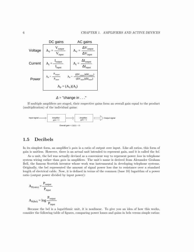
Electrical amplifier gains may be expressed in terms of voltage, current, and/or power, in bothAC and DC. A summary of gain definitions is as follows. The triangle-shaped ”delta” symbol (∆)represents change in mathematics, so ”∆Voutput / ∆Vinput” means ”change in output voltage dividedby change in input voltage,” or more simply, ”AC output voltage divided by AC input voltage”:
6 CHAPTER 1. AMPLIFIERS AND ACTIVE DEVICES
DC gains AC gains
Voltage
Current
Power
AV = Voutput
Vinput
AV = ∆Voutput
∆Vinput
AI =Ioutput
Iinput
AI = ∆Ioutput
∆Iinput
AP = Poutput
Pinput
AP =(∆Voutput)(∆Ioutput)
(∆Vinput)(∆Iinput)
AP = (AV)(AI)
∆ = "change in . . ."
If multiple amplifiers are staged, their respective gains form an overall gain equal to the product(multiplication) of the individual gains:
Amplifiergain = 3
Input signal Output signalAmplifiergain = 5
Overall gain = (3)(5) = 15
1.5 Decibels
In its simplest form, an amplifier’s gain is a ratio of output over input. Like all ratios, this form ofgain is unitless. However, there is an actual unit intended to represent gain, and it is called the bel.
As a unit, the bel was actually devised as a convenient way to represent power loss in telephonesystem wiring rather than gain in amplifiers. The unit’s name is derived from Alexander GrahamBell, the famous Scottish inventor whose work was instrumental in developing telephone systems.Originally, the bel represented the amount of signal power loss due to resistance over a standardlength of electrical cable. Now, it is defined in terms of the common (base 10) logarithm of a powerratio (output power divided by input power):
AP(ratio) = Poutput
Pinput
AP(Bel) = logPoutput
Pinput
Because the bel is a logarithmic unit, it is nonlinear. To give you an idea of how this works,consider the following table of figures, comparing power losses and gains in bels versus simple ratios:

1.5. DECIBELS 7
Loss/gain asa ratio
Loss/gainin bels
1(no loss or gain)
Poutput
Pinput
Poutput
Pinput
log
10
100
1000 3 B
2 B
1 B
0 B
0.1 -1 B
0.01 -2 B
0.001 -3 B
It was later decided that the bel was too large of a unit to be used directly, and so it becamecustomary to apply the metric prefix deci (meaning 1/10) to it, making it decibels, or dB. Now, theexpression ”dB” is so common that many people do not realize it is a combination of ”deci-” and”-bel,” or that there even is such a unit as the ”bel.” To put this into perspective, here is anothertable contrasting power gain/loss ratios against decibels:

8 CHAPTER 1. AMPLIFIERS AND ACTIVE DEVICES
Loss/gain asa ratio
Loss/gain
1(no loss or gain)
Poutput
Pinput
Poutput
Pinput
10
100
1000
0.1
0.01
0.001
10 log
30 dB
20 dB
10 dB
0 dB
-10 dB
-20 dB
-30 dB
in decibels
As a logarithmic unit, this mode of power gain expression covers a wide range of ratios with aminimal span in figures. It is reasonable to ask, ”why did anyone feel the need to invent a logarithmicunit for electrical signal power loss in a telephone system?” The answer is related to the dynamicsof human hearing, the perceptive intensity of which is logarithmic in nature.
Human hearing is highly nonlinear: in order to double the perceived intensity of a sound, theactual sound power must be multiplied by a factor of ten. Relating telephone signal power lossin terms of the logarithmic ”bel” scale makes perfect sense in this context: a power loss of 1 beltranslates to a perceived sound loss of 50 percent, or 1/2. A power gain of 1 bel translates to adoubling in the perceived intensity of the sound.
An almost perfect analogy to the bel scale is the Richter scale used to describe earthquakeintensity: a 6.0 Richter earthquake is 10 times more powerful than a 5.0 Richter earthquake; a 7.0Richter earthquake 100 times more powerful than a 5.0 Richter earthquake; a 4.0 Richter earthquakeis 1/10 as powerful as a 5.0 Richter earthquake, and so on. The measurement scale for chemical pHis likewise logarithmic, a difference of 1 on the scale is equivalent to a tenfold difference in hydrogenion concentration of a chemical solution. An advantage of using a logarithmic measurement scale isthe tremendous range of expression afforded by a relatively small span of numerical values, and it isthis advantage which secures the use of Richter numbers for earthquakes and pH for hydrogen ionactivity.
Another reason for the adoption of the bel as a unit for gain is for simple expression of systemgains and losses. Consider the last system example where two amplifiers were connected tandem toamplify a signal. The respective gain for each amplifier was expressed as a ratio, and the overallgain for the system was the product (multiplication) of those two ratios:
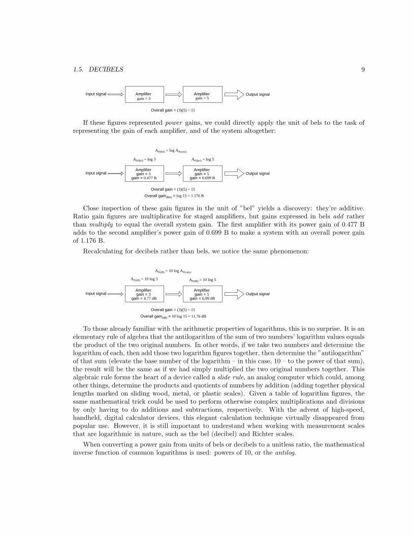
1.5. DECIBELS 9
Amplifiergain = 3
Input signal Output signalAmplifiergain = 5
Overall gain = (3)(5) = 15
If these figures represented power gains, we could directly apply the unit of bels to the task ofrepresenting the gain of each amplifier, and of the system altogether:
AmplifierInput signal Output signal
Amplifier
Overall gain = (3)(5) = 15
AP(Bel) = log AP(ratio)
AP(Bel) = log 3 AP(Bel) = log 5
gain = 3 gain = 5gain = 0.477 B gain = 0.699 B
Overall gain(Bel) = log 15 = 1.176 B
Close inspection of these gain figures in the unit of ”bel” yields a discovery: they’re additive.Ratio gain figures are multiplicative for staged amplifiers, but gains expressed in bels add ratherthan multiply to equal the overall system gain. The first amplifier with its power gain of 0.477 Badds to the second amplifier’s power gain of 0.699 B to make a system with an overall power gainof 1.176 B.
Recalculating for decibels rather than bels, we notice the same phenomenon:
AmplifierInput signal Output signal
Amplifier
Overall gain = (3)(5) = 15
gain = 3 gain = 5
AP(dB) = 10 log AP(ratio)
AP(dB) = 10 log 3 AP(dB) = 10 log 5
gain = 4.77 dB gain = 6.99 dB
Overall gain(dB) = 10 log 15 = 11.76 dB
To those already familiar with the arithmetic properties of logarithms, this is no surprise. It is anelementary rule of algebra that the antilogarithm of the sum of two numbers’ logarithm values equalsthe product of the two original numbers. In other words, if we take two numbers and determine thelogarithm of each, then add those two logarithm figures together, then determine the ”antilogarithm”of that sum (elevate the base number of the logarithm – in this case, 10 – to the power of that sum),the result will be the same as if we had simply multiplied the two original numbers together. Thisalgebraic rule forms the heart of a device called a slide rule, an analog computer which could, amongother things, determine the products and quotients of numbers by addition (adding together physicallengths marked on sliding wood, metal, or plastic scales). Given a table of logarithm figures, thesame mathematical trick could be used to perform otherwise complex multiplications and divisionsby only having to do additions and subtractions, respectively. With the advent of high-speed,handheld, digital calculator devices, this elegant calculation technique virtually disappeared frompopular use. However, it is still important to understand when working with measurement scalesthat are logarithmic in nature, such as the bel (decibel) and Richter scales.
When converting a power gain from units of bels or decibels to a unitless ratio, the mathematicalinverse function of common logarithms is used: powers of 10, or the antilog.

10 CHAPTER 1. AMPLIFIERS AND ACTIVE DEVICES
If:
AP(Bel) = log AP(ratio)
Then:
AP(ratio) = 10AP(Bel)
Converting decibels into unitless ratios for power gain is much the same, only a division factorof 10 is included in the exponent term:
If:
Then:
AP(dB) = 10 log AP(ratio)
AP(ratio) = 10
AP(dB)
10
Because the bel is fundamentally a unit of power gain or loss in a system, voltage or currentgains and losses don’t convert to bels or dB in quite the same way. When using bels or decibels toexpress a gain other than power, be it voltage or current, we must perform the calculation in termsof how much power gain there would be for that amount of voltage or current gain. For a constantload impedance, a voltage or current gain of 2 equates to a power gain of 4 (22); a voltage or currentgain of 3 equates to a power gain of 9 (32). If we multiply either voltage or current by a given factor,then the power gain incurred by that multiplication will be the square of that factor. This relatesback to the forms of Joule’s Law where power was calculated from either voltage or current, andresistance:
P = I2R
P =E2
R
Power is proportional to the squareof either voltage or current
Thus, when translating a voltage or current gain ratio into a respective gain in terms of the belunit, we must include this exponent in the equation(s):
Exponent required
AP(Bel) = log AP(ratio)
AV(Bel) = log AV(ratio)2
AI(Bel) = log AI(ratio)2
The same exponent requirement holds true when expressing voltage or current gains in terms ofdecibels:
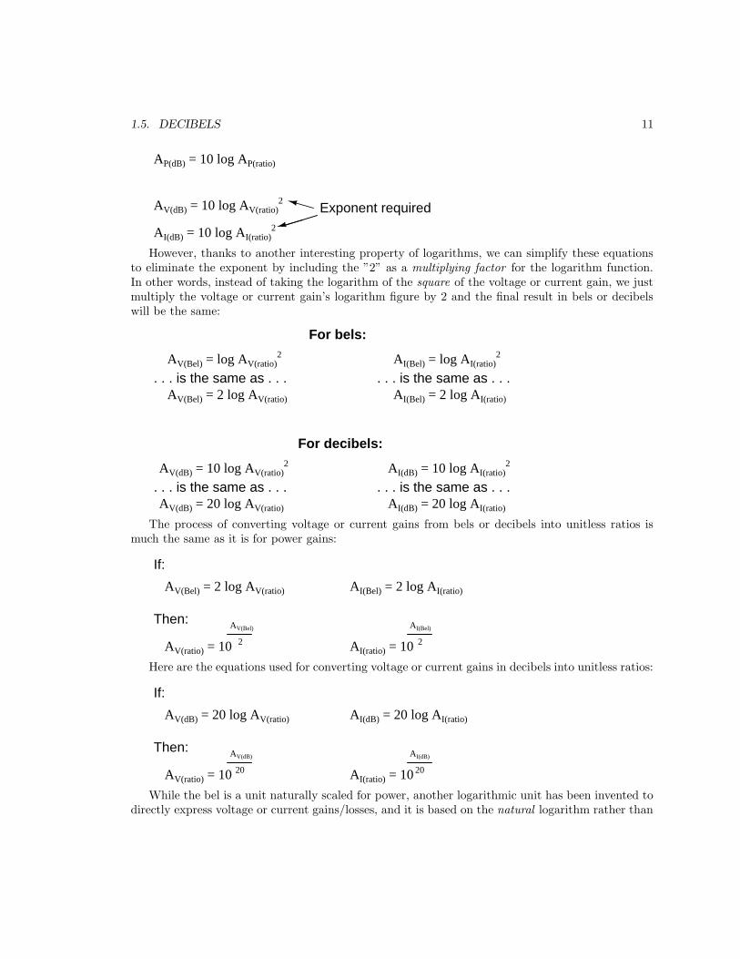
1.5. DECIBELS 11
Exponent required
AP(dB) = 10 log AP(ratio)
AV(dB) = 10 log AV(ratio)2
AI(dB) = 10 log AI(ratio)2
However, thanks to another interesting property of logarithms, we can simplify these equationsto eliminate the exponent by including the ”2” as a multiplying factor for the logarithm function.In other words, instead of taking the logarithm of the square of the voltage or current gain, we justmultiply the voltage or current gain’s logarithm figure by 2 and the final result in bels or decibelswill be the same:
AI(dB) = 10 log AI(ratio)2
. . . is the same as . . .AV(Bel) = log AV(ratio)
2
AV(Bel) = 2 log AV(ratio)
AI(Bel) = log AI(ratio)2
. . . is the same as . . .AI(Bel) = 2 log AI(ratio)
For bels:
For decibels:
. . . is the same as . . . . . . is the same as . . .AI(dB) = 20 log AI(ratio)
AV(dB) = 10 log AV(ratio)2
AV(dB) = 20 log AV(ratio)
The process of converting voltage or current gains from bels or decibels into unitless ratios ismuch the same as it is for power gains:
If:
Then:
AV(Bel) = 2 log AV(ratio)
AV(ratio) = 10 2
AV(Bel)
AI(Bel) = 2 log AI(ratio)
AI(ratio) = 10
AI(Bel)
2
Here are the equations used for converting voltage or current gains in decibels into unitless ratios:
If:
Then:
AV(dB) = 20 log AV(ratio)
AV(ratio) = 10
AV(dB)
20 20
AI(dB) = 20 log AI(ratio)
AI(ratio) = 10
AI(dB)
While the bel is a unit naturally scaled for power, another logarithmic unit has been invented todirectly express voltage or current gains/losses, and it is based on the natural logarithm rather than

12 CHAPTER 1. AMPLIFIERS AND ACTIVE DEVICES
the common logarithm as bels and decibels are. Called the neper, its unit symbol is a lower-case”n.”
AV(neper) = ln AV(ratio)
AV(ratio) = Voutput
Vinput
AI(ratio) =Ioutput
Iinput
AI(neper) = ln AI(ratio)
For better or for worse, neither the neper nor its attenuated cousin, the decineper, is popularlyused as a unit in American engineering applications.
• REVIEW:
• Gains and losses may be expressed in terms of a unitless ratio, or in the unit of bels (B) ordecibels (dB). A decibel is literally a deci -bel: one-tenth of a bel.
• The bel is fundamentally a unit for expressing power gain or loss. To convert a power ratio toeither bels or decibels, use one of these equations:
• AP(Bel) = log AP(ratio) AP(db) = 10 log AP(ratio)
• When using the unit of the bel or decibel to express a voltage or current ratio, it must be castin terms of the an equivalent power ratio. Practically, this means the use of different equations,with a multiplication factor of 2 for the logarithm value corresponding to an exponent of 2 forthe voltage or current gain ratio:
•
AV(Bel) = 2 log AV(ratio) AV(dB) = 20 log AV(ratio)
AI(Bel) = 2 log AI(ratio) AI(dB) = 20 log AI(ratio)
• To convert a decibel gain into a unitless ratio gain, use one of these equations:
•
AV(ratio) = 10
AV(dB)
20
20AI(ratio) = 10
AI(dB)
AP(ratio) = 10
AP(dB)
10
• A gain (amplification) is expressed as a positive bel or decibel figure. A loss (attenuation) isexpressed as a negative bel or decibel figure. Unity gain (no gain or loss; ratio = 1) is expressedas zero bels or zero decibels.
• When calculating overall gain for an amplifier system composed of multiple amplifier stages,individual gain ratios are multiplied to find the overall gain ratio. Bel or decibel figures foreach amplifier stage, on the other hand, are added together to determine overall gain.

1.6. ABSOLUTE DB SCALES 13
1.6 Absolute dB scales
It is also possible to use the decibel as a unit of absolute power, in addition to using it as an expressionof power gain or loss. A common example of this is the use of decibels as a measurement of soundpressure intensity. In cases like these, the measurement is made in reference to some standardizedpower level defined as 0 dB. For measurements of sound pressure, 0 dB is loosely defined as thelower threshold of human hearing, objectively quantified as 1 picowatt of sound power per squaremeter of area.A sound measuring 40 dB on the decibel sound scale would be 104 times greater than the
threshold of hearing. A 100 dB sound would be 1010 (ten billion) times greater than the thresholdof hearing.Because the human ear is not equally sensitive to all frequencies of sound, variations of the decibel
sound-power scale have been developed to represent physiologically equivalent sound intensities atdifferent frequencies. Some sound intensity instruments were equipped with filter networks to givedisproportionate indications across the frequency scale, the intent of which to better represent theeffects of sound on the human body. Three filtered scales became commonly known as the ”A,” ”B,”and ”C” weighted scales. Decibel sound intensity indications measured through these respectivefiltering networks were given in units of dBA, dBB, and dBC. Today, the ”A-weighted scale” ismost commonly used for expressing the equivalent physiological impact on the human body, and isespecially useful for rating dangerously loud noise sources.Another standard-referenced system of power measurement in the unit of decibels has been
established for use in telecommunications systems. This is called the dBm scale. The referencepoint, 0 dBm, is defined as 1 milliwatt of electrical power dissipated by a 600 Ω load. Accordingto this scale, 10 dBm is equal to 10 times the reference power, or 10 milliwatts; 20 dBm is equal to100 times the reference power, or 100 milliwatts. Some AC voltmeters come equipped with a dBmrange or scale (sometimes labeled ”DB”) intended for use in measuring AC signal power across a600 Ω load. 0 dBm on this scale is, of course, elevated above zero because it represents somethinggreater than 0 (actually, it represents 0.7746 volts across a 600 Ω load, voltage being equal to thesquare root of power times resistance; the square root of 0.001 multiplied by 600). When viewedon the face of an analog meter movement, this dBm scale appears compressed on the left side andexpanded on the right in a manner not unlike a resistance scale, owing to its logarithmic nature.An adaptation of the dBm scale for audio signal strength is used in studio recording and broadcast
engineering for standardizing volume levels, and is called the VU scale. VU meters are frequentlyseen on electronic recording instruments to indicate whether or not the recorded signal exceeds themaximum signal level limit of the device, where significant distortion will occur. This ”volumeindicator” scale is calibrated in according to the dBm scale, but does not directly indicate dBm forany signal other than steady sine-wave tones. The proper unit of measurement for a VU meter isvolume units.When relatively large signals are dealt with, and an absolute dB scale would be useful for rep-
resenting signal level, specialized decibel scales are sometimes used with reference points greaterthan the 1mW used in dBm. Such is the case for the dBW scale, with a reference point of 0 dBWestablished at 1 watt. Another absolute measure of power called the dBk scale references 0 dBk at1 kW, or 1000 watts.
• REVIEW:
• The unit of the bel or decibel may also be used to represent an absolute measurement of power

14 CHAPTER 1. AMPLIFIERS AND ACTIVE DEVICES
rather than just a relative gain or loss. For sound power measurements, 0 dB is defined as astandardized reference point of power equal to 1 picowatt per square meter. Another dB scalesuited for sound intensity measurements is normalized to the same physiological effects as a1000 Hz tone, and is called the dBA scale. In this system, 0 dBA is defined as any frequencysound having the same physiological equivalence as a 1 picowatt-per-square-meter tone at 1000Hz.
• An electrical dB scale with an absolute reference point has been made for use in telecommu-nications systems. Called the dBm scale, its reference point of 0 dBm is defined as 1 milliwattof AC signal power dissipated by a 600 Ω load.
• A VU meter reads audio signal level according to the dBm for sine-wave signals. Becauseits response to signals other than steady sine waves is not the same as true dBm, its unit ofmeasurement is volume units.
• dB scales with greater absolute reference points than the dBm scale have been invented forhigh-power signals. The dBW scale has its reference point of 0 dBW defined as 1 watt ofpower. The dBk scale sets 1 kW (1000 watts) as the zero-point reference.
1.7 Contributors
Contributors to this chapter are listed in chronological order of their contributions, from most recentto first. See Appendix 2 (Contributor List) for dates and contact information.
Colin Barnard (November 2003): Correction regarding Alexander Graham Bell’s country oforigin (Scotland, not the United States).

Chapter 2
SOLID-STATE DEVICE THEORY
Contents
2.1 Introduction . . . . . . . . . . . . . . . . . . . . . . . . . . . . . . . . . . 15
2.2 Quantum physics . . . . . . . . . . . . . . . . . . . . . . . . . . . . . . . . 15
2.3 Band theory of solids . . . . . . . . . . . . . . . . . . . . . . . . . . . . . 27
2.4 Electrons and ”holes” . . . . . . . . . . . . . . . . . . . . . . . . . . . . . 30
2.5 The P-N junction . . . . . . . . . . . . . . . . . . . . . . . . . . . . . . . 30
2.6 Junction diodes . . . . . . . . . . . . . . . . . . . . . . . . . . . . . . . . 30
2.7 Bipolar junction transistors . . . . . . . . . . . . . . . . . . . . . . . . . 31
2.8 Junction field-effect transistors . . . . . . . . . . . . . . . . . . . . . . . 32
2.9 Insulated-gate field-effect transistors . . . . . . . . . . . . . . . . . . . . 33
2.10 Thyristors . . . . . . . . . . . . . . . . . . . . . . . . . . . . . . . . . . . . 34
2.11 Semiconductor manufacturing techniques . . . . . . . . . . . . . . . . . 34
2.12 Superconducting devices . . . . . . . . . . . . . . . . . . . . . . . . . . . 34
2.13 Quantum devices . . . . . . . . . . . . . . . . . . . . . . . . . . . . . . . . 35
2.14 Semiconductor devices in SPICE . . . . . . . . . . . . . . . . . . . . . . 35
2.15 Contributors . . . . . . . . . . . . . . . . . . . . . . . . . . . . . . . . . . 35
*** INCOMPLETE ***
2.1 Introduction
This chapter will cover the physics behind the operation of semiconductor devices and show howthese principles are applied in several different types of semiconductor devices. Subsequent chapterswill deal primarily with the practical aspects of these devices in circuits and omit theory as muchas possible.
2.2 Quantum physics
”I think it is safe to say that no one understands quantum mechanics.”
15

16 CHAPTER 2. SOLID-STATE DEVICE THEORY
Physicist Richard P. Feynman
To say that the invention of semiconductor devices was a revolution would not be an exaggeration.Not only was this an impressive technological accomplishment, but it paved the way for develop-ments that would indelibly alter modern society. Semiconductor devices made possible miniaturizedelectronics, including computers, certain types of medical diagnostic and treatment equipment, andpopular telecommunication devices, to name a few applications of this technology.But behind this revolution in technology stands an even greater revolution in general science: the
field of quantum physics. Without this leap in understanding the natural world, the development ofsemiconductor devices (and more advanced electronic devices still under development) would neverhave been possible. Quantum physics is an incredibly complicated realm of science, and this chapteris by no means a complete discussion of it, but rather a brief overview. When scientists of Feynman’scaliber say that ”no one understands [it],” you can be sure it is a complex subject. Without a basicunderstanding of quantum physics, or at least an understanding of the scientific discoveries that led toits formulation, though, it is impossible to understand how and why semiconductor electronic devicesfunction. Most introductory electronics textbooks I’ve read attempt to explain semiconductors interms of ”classical” physics, resulting in more confusion than comprehension.Many of us have seen diagrams of atoms that look something like this:
N
N
N
N
NN
P
PP
PP
P
e
e
e e
e
e
e
N
P
= electron
= proton
= neutron
Tiny particles of matter called protons and neutrons make up the center of the atom, whileelectrons orbit around not unlike planets around a star. The nucleus carries a positive electricalcharge, owing to the presence of protons (the neutrons have no electrical charge whatsoever), whilethe atom’s balancing negative charge resides in the orbiting electrons. The negative electrons tendto be attracted to the positive protons just as planets are gravitationally attracted toward whateverobject(s) they orbit, yet the orbits are stable due to the electrons’ motion. We owe this popularmodel of the atom to the work of Ernest Rutherford, who around the year 1911 experimentallydetermined that atoms’ positive charges were concentrated in a tiny, dense core rather than beingspread evenly about the diameter as was proposed by an earlier researcher, J.J. Thompson.While Rutherford’s atomic model accounted for experimental data better than Thompson’s, it
still wasn’t perfect. Further attempts at defining atomic structure were undertaken, and these efforts

2.2. QUANTUM PHYSICS 17
helped pave the way for the bizarre discoveries of quantum physics. Today our understanding ofthe atom is quite a bit more complex. However, despite the revolution of quantum physics and theimpact it had on our understanding of atomic structure, Rutherford’s solar-system picture of theatom embedded itself in the popular conscience to such a degree that it persists in some areas ofstudy even when inappropriate.Consider this short description of electrons in an atom, taken from a popular electronics textbook:
Orbiting negative electrons are therefore attracted toward the positive nucleus, whichleads us to the question of why the electrons do not fly into the atom’s nucleus. Theanswer is that the orbiting electrons remain in their stable orbit due to two equal butopposite forces. The centrifugal outward force exerted on the electrons due to the orbitcounteracts the attractive inward force (centripetal) trying to pull the electrons towardthe nucleus due to the unlike charges.
In keeping with the Rutherford model, this author casts the electrons as solid chunks of matterengaged in circular orbits, their inward attraction to the oppositely charged nucleus balanced by theirmotion. The reference to ”centrifugal force” is technically incorrect (even for orbiting planets), butis easily forgiven due to its popular acceptance: in reality, there is no such thing as a force pushingany orbiting body away from its center of orbit. It only seems that way because a body’s inertiatends to keep it traveling in a straight line, and since an orbit is a constant deviation (acceleration)from straight-line travel, there is constant inertial opposition to whatever force is attracting thebody toward the orbit center (centripetal), be it gravity, electrostatic attraction, or even the tensionof a mechanical link.The real problem with this explanation, however, is the idea of electrons traveling in circular
orbits in the first place. It is a verifiable fact that accelerating electric charges emit electromagneticradiation, and this fact was known even in Rutherford’s time. Since orbiting motion is a form ofacceleration (the orbiting object in constant acceleration away from normal, straight-line motion),electrons in an orbiting state should be throwing off radiation like mud from a spinning tire. Electronsaccelerated around circular paths in particle accelerators called synchrotrons are known to do this,and the result is called synchrotron radiation. If electrons were losing energy in this way, their orbitswould eventually decay, resulting in collisions with the positively charged nucleus. However, thisdoesn’t ordinarily happen within atoms. Indeed, electron ”orbits” are remarkably stable over a widerange of conditions.Furthermore, experiments with ”excited” atoms demonstrated that electromagnetic energy emit-
ted by an atom occurs only at certain, definite frequencies. Atoms that are ”excited” by outsideinfluences such as light are known to absorb that energy and return it as electromagnetic waves ofvery specific frequencies, like a tuning fork that rings at a fixed pitch no matter how it is struck.When the light emitted by an excited atom is divided into its constituent frequencies (colors) by aprism, distinct lines of color appear in the spectrum, the pattern of spectral lines being unique tothat element. So regular is this phenomenon that it is commonly used to identify atomic elements,and even measure the proportions of each element in a compound or chemical mixture. Accordingto Rutherford’s solar-system atomic model (regarding electrons as chunks of matter free to orbit atany radius) and the laws of classical physics, excited atoms should be able to return energy overa virtually limitless range of frequencies rather than a select few. In other words, if Rutherford’smodel were correct, there would be no ”tuning fork” effect, and the light spectrum emitted by anyatom would appear as a continuous band of colors rather than as a few distinct lines.

18 CHAPTER 2. SOLID-STATE DEVICE THEORY
A pioneering researcher by the name of Niels Bohr attempted to improve upon Rutherford’smodel after studying in Rutherford’s laboratory for several months in 1912. Trying to harmonizethe findings of other physicists (most notably, Max Planck and Albert Einstein), Bohr suggestedthat each electron possessed a certain, specific amount of energy, and that their orbits were likewisequantized such that they could only occupy certain places around the nucleus, somewhat like marblesfixed in circular tracks around the nucleus rather than the free-ranging satellites they were formerlyimagined to be. In deference to the laws of electromagnetics and accelerating charges, Bohr referredto these ”orbits” as stationary states so as to escape the implication that they were in motion.
While Bohr’s ambitious attempt at re-framing the structure of the atom in terms that agreedcloser to experimental results was a milestone in physics, it was by no means complete. His math-ematical analyses produced better predictions of experimental events than analyses belonging toprevious models, but there were still some unanswered questions as to why electrons would behavein such strange ways. The assertion that electrons existed in stationary, quantized states aroundthe nucleus certainly accounted for experimental data better than Rutherford’s model, but he hadno idea what would force electrons to manifest those particular states. The answer to that questionhad to come from another physicist, Louis de Broglie, about a decade later.
De Broglie proposed that electrons, like photons (particles of light) manifested both particle-like and wave-like properties. Building on this proposal, he suggested that an analysis of orbitingelectrons from a wave perspective rather than a particle perspective might make more sense oftheir quantized nature. Indeed, this was the case, and another breakthrough in understanding wasreached.
The atom according to de Broglie consisted of electrons existing in the form of standing waves,a phenomenon well known to physicists in a variety of forms. Like the plucked string of a musicalinstrument vibrating at a resonant frequency, with ”nodes” and ”antinodes” at stable positions alongits length, de Broglie envisioned electrons around atoms standing as waves bent around a circle:
antinode antinode
nodenode node
String vibrating at resonant frequency betweentwo fixed points forms a standing wave.

2.2. QUANTUM PHYSICS 19
nucleus
antinode antinode
antinodeantinode
node node
node
node
"Orbiting" electron as a standing wave aroundthe nucleus. Two cycles per "orbit" shown.
nucleus
antinode
node
"Orbiting" electron as a standing wave aroundthe nucleus. Three cycles per "orbit" shown.
antinode
antinode
antinodeantinode
antinode
node
node
node
node
node
Electrons could only exist in certain, definite ”orbits” around the nucleus because those were theonly distances where the wave ends would match. In any other radius, the wave would destructivelyinterfere with itself and thus cease to exist.De Broglie’s hypothesis gave both mathematical support and a convenient physical analogy
to account for the quantized states of electrons within an atom, but his atomic model was stillincomplete. Within a few years, though, physicists Werner Heisenberg and Erwin Schrodinger,working independently of each other, built upon de Broglie’s concept of a matter-wave duality tocreate more mathematically rigorous models of subatomic particles.This theoretical advance from de Broglie’s primitive standing wave model to Heisenberg’s ma-
trix and Schrodinger’s differential equation models was given the name quantum mechanics, and it

20 CHAPTER 2. SOLID-STATE DEVICE THEORY
introduced a rather shocking characteristic to the world of subatomic particles: the trait of prob-ability, or uncertainty. According to the new quantum theory, it was impossible to determine theexact position and exact momentum of a particle at the same time. Popular explanations of this”uncertainty principle” usually cast it in terms of error caused by the process of measurement (i.e.by attempting to precisely measure the position of an electron, you interfere with its momentumand thus cannot know what it was before the position measurement was taken, and visa versa), butthe truth is actually much more mysterious than simple measurement interference. The startlingimplication of quantum mechanics is that particles do not actually possess precise positions andmomenta, but rather balance the two quantities in a such way that their combined uncertaintiesnever diminish below a certain minimum value.It is interesting to note that this form of ”uncertainty” relationship exists in areas other than
quantum mechanics. As discussed in the ”Mixed-Frequency AC Signals” chapter in volume II ofthis book series, there is a mutually exclusive relationship between the certainty of a waveform’stime-domain data and its frequency-domain data. In simple terms, the more precisely we know itsconstituent frequency(ies), the less precisely we know its amplitude in time, and vice versa. To quotemyself:
A waveform of infinite duration (infinite number of cycles) can be analyzed withabsolute precision, but the less cycles available to the computer for analysis, the lessprecise the analysis. . . The fewer times that a wave cycles, the less certain its frequencyis. Taking this concept to its logical extreme, a short pulse – a waveform that doesn’teven complete a cycle – actually has no frequency, but rather acts as an infinite range offrequencies. This principle is common to all wave-based phenomena, not just AC voltagesand currents.
In order to precisely determine the amplitude of a varying signal, we must sample it over a verynarrow span of time. However, doing this limits our view of the wave’s frequency. Conversely, todetermine a wave’s frequency with great precision, we must sample it over many, many cycles, whichmeans we lose view of its amplitude at any given moment. Thus, we cannot simultaneously know theinstantaneous amplitude and the overall frequency of any wave with unlimited precision. Strangeryet, this uncertainty is much more than observer imprecision; it resides in the very nature of thewave itself. It is not as though it would be possible, given the proper technology, to obtain precisemeasurements of both instantaneous amplitude and frequency at once. Quite literally, a wave cannotpossess both a precise, instantaneous amplitude, and a precise frequency at the same time.Likewise, the minimum uncertainty of a particle’s position and momentum expressed by Heisen-
berg and Schrodinger has nothing to do with limitation in measurement; rather it is an intrinsicproperty of the particle’s matter-wave dual nature. Electrons, therefore, do not really exist in their”orbits” as precisely defined bits of matter, or even as precisely defined waveshapes, but rather as”clouds” – the technical term is wavefunction – of probability distribution, as if each electron were”spread” or ”smeared” over a range of positions and momenta.This radical view of electrons as imprecise clouds at first seems to contradict the original principle
of quantized electron states: that electrons exist in discrete, defined ”orbits” around atomic nuclei.It was, after all, this discovery that led to the formation of quantum theory to explain it. Howodd it seems that a theory developed to explain the discrete behavior of electrons ends up declaringthat electrons exist as ”clouds” rather than as discrete pieces of matter. However, the quantizedbehavior of electrons does not depend on electrons having definite position and momentum values,

2.2. QUANTUM PHYSICS 21
but rather on other properties called quantum numbers. In essence, quantum mechanics dispenseswith commonly held notions of absolute position and absolute momentum, and replaces them withabsolute notions of a sort having no analogue in common experience.
Even though electrons are known to exist in ethereal, ”cloud-like” forms of distributed probabil-ity rather than as discrete chunks of matter, those ”clouds” possess other characteristics that arediscrete. Any electron in an atom can be described in terms of four numerical measures (the previ-ously mentioned quantum numbers), called the Principal, Angular Momentum,Magnetic, andSpin numbers. The following is a synopsis of each of these numbers’ meanings:
Principal Quantum Number: Symbolized by the letter n, this number describes the shellthat an electron resides in. An electron ”shell” is a region of space around an atom’s nucleus thatelectrons are allowed to exist in, corresponding to the stable ”standing wave” patterns of de Broglieand Bohr. Electrons may ”leap” from shell to shell, but cannot exist between the shell regions.
The principle quantum number can be any positive integer (a whole number, greater than orequal to 1). In other words, there is no such thing as a principle quantum number for an electronof 1/2 or -3. These integer values were not arrived at arbitrarily, but rather through experimentalevidence of light spectra: the differing frequencies (colors) of light emitted by excited hydrogenatoms follow a sequence mathematically dependent on specific, integer values.
Each shell has the capacity to hold multiple electrons. An analogy for electron shells is theconcentric rows of seats of an amphitheater. Just as a person seated in an amphitheater must choosea row to sit in (for there is no place to sit in the space between rows), electrons must ”choose” aparticular shell to ”sit” in. Like amphitheater rows, the outermost shells are able to hold moreelectrons than the inner shells. Also, electrons tend to seek the lowest available shell, like people inan amphitheater trying to find the closest seat to the center stage. The higher the shell number,the greater the energy of the electrons in it.
The maximum number of electrons that any shell can hold is described by the equation 2n2,where ”n” is the principle quantum number. Thus, the first shell (n=1) can hold 2 electrons; thesecond shell (n=2) 8 electrons, and the third shell (n=3) 18 electrons.
Electron shells in an atom are sometimes designated by letter rather than by number. The firstshell (n=1) is labeled K, the second shell (n=2) L, the third shell (n=3) M, the fourth shell (n=4)N, the fifth shell (n=5) O, the sixth shell (n=6) P, and the seventh shell (n=7) Q.
Angular Momentum Quantum Number: Within each shell, there are subshells. One mightbe inclined to think of subshells as simple subdivisions of shells, like lanes dividing a road, but thetruth is much stranger than this. Subshells are regions of space where electron ”clouds” are allowed toexist, and different subshells actually have different shapes. The first subshell is shaped like a sphere,which makes sense to most people, visualizing a cloud of electrons surrounding the atomic nucleusin three dimensions. The second subshell, however, resembles a dumbbell, comprised of two ”lobes”joined together at a single point near the atom’s center. The third subshell typically resembles aset of four ”lobes” clustered around the atom’s nucleus. These subshell shapes are reminiscent ofgraphical depictions of radio antenna signal strength, with bulbous lobe-shaped regions extendingfrom the antenna in various directions.
Valid angular momentum quantum numbers are positive integers like principal quantum numbers,but also include zero. These quantum numbers for electrons are symbolized by the letter l. Thenumber of subshells in a shell is equal to the shell’s principal quantum number. Thus, the first shell

22 CHAPTER 2. SOLID-STATE DEVICE THEORY
(n=1) has one subshell, numbered 0; the second shell (n=2) has two subshells, numbered 0 and 1;the third shell (n=3) has three subshells, numbered 0, 1, and 2.
An older convention for subshell description used letters rather than numbers. In this notationalsystem, the first subshell (l=0) was designated s, the second subshell (l=1) designated p, the thirdsubshell (l=2) designated d, and the fourth subshell (l=3) designated f. The letters come from thewords sharp, principal (not to be confused with the principal quantum number, n), diffuse, andfundamental. You will still see this notational convention in many periodic tables, used to designatethe electron configuration of the atoms’ outermost, or valence, shells.
Magnetic Quantum Number: The magnetic quantum number for an electron classifies whichorientation its subshell shape is pointed. For each subshell in each shell, there are multiple directionsin which the ”lobes” can point, and these different orientations are called orbitals. For the firstsubshell (s; l=0), which resembles a sphere, there is no ”direction” it can ”point,” so there is onlyone orbital. For the second (p; l=1) subshell in each shell, which resembles a dumbbell, there arethree different directions they can be oriented (think of three dumbbells intersecting in the middle,each oriented along a different axis in a three-axis coordinate system).
Valid numerical values for this quantum number consist of integers ranging from -l to l, andare symbolized as ml in atomic physics and lz in nuclear physics. To calculate the number oforbitals in any given subshell, double the subshell number and add 1 (2l + 1). For example, the firstsubshell (l=0) in any shell contains a single orbital, numbered 0; the second subshell (l=1) in anyshell contains three orbitals, numbered -1, 0, and 1; the third subshell (l=2) contains five orbitals,numbered -2, -1, 0, 1, and 2; and so on.
Like principal quantum numbers, the magnetic quantum number arose directly from experimentalevidence: the division of spectral lines as a result of exposing an ionized gas to a magnetic field,hence the name ”magnetic” quantum number.
Spin Quantum Number: Like the magnetic quantum number, this property of atomic elec-trons was discovered through experimentation. Close observation of spectral lines revealed that eachline was actually a pair of very closely-spaced lines, and this so-called fine structure was hypothesizedto be the result of each electron ”spinning” on an axis like a planet. Electrons with different ”spins”would give off slightly different frequencies of light when excited, and so the quantum number of”spin” came to be named as such. The concept of a spinning electron is now obsolete, being bettersuited to the (incorrect) view of electrons as discrete chunks of matter rather than as the ”clouds”they really are, but the name remains.
Spin quantum numbers are symbolized as ms in atomic physics and sz in nuclear physics. Foreach orbital in each subshell in each shell, there can be two electrons, one with a spin of +1/2 andthe other with a spin of -1/2.
The physicist Wolfgang Pauli developed a principle explaining the ordering of electrons in anatom according to these quantum numbers. His principle, called the Pauli exclusion principle, statesthat no two electrons in the same atom may occupy the exact same quantum states. That is, eachelectron in an atom has a unique set of quantum numbers. This limits the number of electrons thatmay occupy any given orbital, subshell, and shell.
Shown here is the electron arrangement for a hydrogen atom:

2.2. QUANTUM PHYSICS 23
HydrogenAtomic number (Z) = 1(one proton in nucleus)
K shell(n = 1)
subshell(l)
orbital(ml)
spin(ms)
0 0 1/2 One electron
Spectroscopic notation: 1s1
With one proton in the nucleus, it takes one electron to electrostatically balance the atom (theproton’s positive electric charge exactly balanced by the electron’s negative electric charge). Thisone electron resides in the lowest shell (n=1), the first subshell (l=0), in the only orbital (spatialorientation) of that subshell (ml=0), with a spin value of 1/2. A very common method of describingthis organization is by listing the electrons according to their shells and subshells in a conventioncalled spectroscopic notation. In this notation, the shell number is shown as an integer, the subshellas a letter (s,p,d,f), and the total number of electrons in the subshell (all orbitals, all spins) as asuperscript. Thus, hydrogen, with its lone electron residing in the base level, would be described as1s1.
Proceeding to the next atom type (in order of atomic number), we have the element helium:
K shell(n = 1)
subshell(l)
orbital(ml)
spin(ms)
0 0 1/2
Spectroscopic notation:
HeliumAtomic number (Z) = 2(two protons in nucleus)
0 0 -1/2 electron
electron
1s2
A helium atom has two protons in the nucleus, and this necessitates two electrons to balance thedouble-positive electric charge. Since two electrons – one with spin=1/2 and the other with spin=-1/2 – will fit into one orbital, the electron configuration of helium requires no additional subshellsor shells to hold the second electron.
However, an atom requiring three or more electrons will require additional subshells to hold allelectrons, since only two electrons will fit into the lowest shell (n=1). Consider the next atom in thesequence of increasing atomic numbers, lithium:

24 CHAPTER 2. SOLID-STATE DEVICE THEORY
K shell(n = 1)
subshell(l)
orbital(ml)
spin(ms)
0 0 1/2
Spectroscopic notation:
0 0 -1/2 electron
electron
LithiumAtomic number (Z) = 3
L shell(n = 2)
0 0 1/2 electron
1s22s1
An atom of lithium only uses a fraction of the L shell’s (n=2) capacity. This shell actuallyhas a total capacity of eight electrons (maximum shell capacity = 2n2 electrons). If we examinethe organization of the atom with a completely filled L shell, we will see how all combinations ofsubshells, orbitals, and spins are occupied by electrons:
K shell(n = 1)
subshell(l)
orbital(ml)
spin(ms)
0 0 1/2
0 0 -1/2
L shell(n = 2)
0 0 1/2
NeonAtomic number (Z) = 10
0 0 -1/2
1
1
1
1
1
1
-1 1/2
-1 -1/2
0
0
-1/21/2
1
1 -1/21/2
s subshell(l = 0)
s subshell(l = 0)
p subshell(l = 1)
2 electrons
2 electrons
6 electrons
Spectroscopic notation: 1s22s22p6
Often, when the spectroscopic notation is given for an atom, any shells that are completely filledare omitted, and only the unfilled, or the highest-level filled shell, is denoted. For example, theelement neon (shown in the previous illustration), which has two completely filled shells, may be

2.2. QUANTUM PHYSICS 25
spectroscopically described simply as 2p6 rather than 1s22s22p6. Lithium, with its K shell completelyfilled and a solitary electron in the L shell, may be described simply as 2s1 rather than 1s22s1.
The omission of completely filled, lower-level shells is not just a notational convenience. Italso illustrates a basic principle of chemistry: that the chemical behavior of an element is primarilydetermined by its unfilled shells. Both hydrogen and lithium have a single electron in their outermostshells (1s1 and 2s1, respectively), and this gives the two elements some similar properties. Both arehighly reactive, and reactive in much the same way (bonding to similar elements in similar modes).It matters little that lithium has a completely filled K shell underneath its almost-vacant L shell:the unfilled L shell is the shell that determines its chemical behavior.
Elements having completely filled outer shells are classified as noble, and are distinguished bytheir almost complete non-reactivity with other elements. These elements used to be classified asinert, when it was thought that they were completely unreactive, but it is now known that they mayform compounds with other elements under certain conditions.
Given the fact that elements with identical electron configurations in their outermost shell(s)exhibit similar chemical properties, it makes sense to organize the different elements in a tableaccordingly. Such a table is known as a periodic table of the elements, and modern tables follow thisgeneral form:
PotassiumK 19
39.0983
4s1
CalciumCa 20
4s2
NaSodium
11
3s1
MagnesiumMg 12
3s2
H 1Hydrogen
1s1
LiLithium6.941
3
2s1
BerylliumBe 4
2s2
Sc 21Scandium
3d14s2
Ti 22Titanium
3d24s2
V 23Vanadium50.9415
3d34s2
Cr 24Chromium
3d54s1
Mn 25Manganese
3d54s2
Fe 26Iron
55.847
3d64s2
Co 27Cobalt
3d74s2
Ni 28Nickel
3d84s2
Cu 29Copper63.546
3d104s1
Zn 30Zinc
3d104s2
Ga 31Gallium
4p1
B 5Boron10.81
2p1
C 6Carbon12.011
2p2
N 7Nitrogen14.0067
2p3
O 8Oxygen15.9994
2p4
F 9Fluorine18.9984
2p5
He 2Helium
4.00260
1s2
Ne 10Neon
20.179
2p6
Ar 18Argon
39.948
3p6
Kr 36Krypton83.80
4p6
Xe 54Xenon131.30
5p6
Rn 86Radon(222)
6p6
KPotassium
19
39.0983
4s1
Symbol Atomic number
NameAtomic mass
Electronconfiguration Al 13
Aluminum26.9815
3p1
Si 14Silicon
28.0855
3p2
P 15Phosphorus
30.9738
3p3
S 16Sulfur32.06
3p4
Cl 17Chlorine35.453
3p5
Periodic Table of the Elements
Germanium
4p2
Ge 32 AsArsenic
33
4p3
SeSelenium
34
78.96
4p4
BrBromine
35
79.904
4p5
IIodine
53
126.905
5p5
Rubidium37
85.4678
5s1
SrStrontium
38
87.62
5s2
YttriumY 39
4d15s2
Zr 40Zirconium91.224
4d25s2
Nb 41Niobium92.90638
4d45s1
Mo 42Molybdenum
95.94
4d55s1
Tc 43Technetium
(98)
4d55s2
Ru 44Ruthenium
101.07
4d75s1
Rh 45Rhodium
4d85s1
Pd 46Palladium106.42
4d105s0
Ag 47Silver
107.8682
4d105s1
Cd 48Cadmium112.411
4d105s2
In 49Indium114.82
5p1
Sn 50Tin
118.710
5p2
Sb 51Antimony
121.75
5p3
Te 52Tellurium
127.60
5p4
Po 84Polonium
(209)
6p4
AtAstatine
85
(210)
6p5
Metals
Metalloids Nonmetals
Rb
Cs 55Cesium
132.90543
6s1
Ba 56Barium137.327
6s2
57 - 71Lanthanide
series
Hf 72Hafnium178.49
5d26s2
TaTantalum
73
180.9479
5d36s2
W 74Tungsten183.85
5d46s2
Re 75Rhenium186.207
5d56s2
Os 76Osmium
190.2
5d66s2
Ir 77
192.22Iridium
5d76s2
Pt 78Platinum195.08
5d96s1
AuGold
79
196.96654
5d106s1
Hg 80Mercury200.59
5d106s2
Tl 81Thallium204.3833
6p1
PbLead
82
207.2
6p2
BiBismuth
83
208.98037
6p3
Lanthanideseries
Fr 87Francium
(223)
7s1
Ra 88Radium(226)
7s2
89 - 103Actinideseries
Actinideseries
104UnqUnnilquadium
(261)
6d27s2
Unp 105Unnilpentium
(262)
6d37s2
Unh 106Unnilhexium
(263)
6d47s2
Uns 107Unnilseptium
(262)
108 109
1.00794
9.012182
22.989768 24.3050
40.078 44.955910 47.88 51.9961 54.93805 58.93320 58.69 65.39 69.723 72.61 74.92159
88.90585 102.90550
(averaged according tooccurence on earth)
La 57Lanthanum138.9055
5d16s2
Ce 58Cerium140.115
4f15d16s2
Pr 59Praseodymium
140.90765
4f36s2
Nd 60Neodymium
144.24
4f46s2
Pm 61Promethium
(145)
4f56s2
Sm 62Samarium
150.36
4f66s2
Eu 63Europium151.965
4f76s2
Gd 64Gadolinium
157.25
4f75d16s2
Tb 65
158.92534Terbium
4f96s2
Dy 66Dysprosium
162.50
4f106s2
Ho 67Holmium
164.93032
4f116s2
Er 68Erbium167.26
4f126s2
Tm 69Thulium
168.93421
4f136s2
Yb 70Ytterbium
173.04
4f146s2
Lu 71Lutetium174.967
4f145d16s2
AcActinium
89
(227)
6d17s2
Th 90Thorium232.0381
6d27s2
Pa 91Protactinium231.03588
5f26d17s2
U 92Uranium238.0289
5f36d17s2
Np 93Neptunium
(237)
5f46d17s2
Pu 94Plutonium
(244)
5f66d07s2
Am 95Americium
(243)
5f76d07s2
Cm 96Curium(247)
5f76d17s2
Bk 97Berkelium
(247)
5f96d07s2
Cf 98Californium
(251)
5f106d07s2
Es 99Einsteinium
(252)
5f116d07s2
Fm 100Fermium
(257)
5f126d07s2
Md 101Mendelevium
(258)
5f136d07s2
No 102Nobelium
(259)
6d07s2
Lr 103Lawrencium
(260)
6d17s2
Dmitri Mendeleev, a Russian chemist, was the first to develop a periodic table of the elements.Although Mendeleev organized his table according to atomic mass rather than atomic number, andso produced a table that was not quite as useful as modern periodic tables, his development standsas an excellent example of scientific proof. Seeing the patterns of periodicity (similar chemicalproperties according to atomic mass), Mendeleev hypothesized that all elements would fit into thisordered scheme. When he discovered ”empty” spots in the table, he followed the logic of the existingorder and hypothesized the existence of heretofore undiscovered elements. The subsequent discoveryof those elements granted scientific legitimacy to Mendeleev’s hypothesis, further discoveries leading

26 CHAPTER 2. SOLID-STATE DEVICE THEORY
to the form of the periodic table we use today.This is how science should work: hypotheses followed to their logical conclusions, and accepted,
modified, or rejected as determined by the agreement of experimental data to those conclusions.Any fool can formulate a hypothesis after-the-fact to explain existing experimental data, and manydo. What sets a scientific hypothesis apart from post hoc speculation is the prediction of futureexperimental data yet uncollected, and the possibility of disproof as a result of that data. To boldlyfollow a hypothesis to its logical conclusion(s) and dare to predict the results of future experimentsis not a dogmatic leap of faith, but rather a public test of that hypothesis, open to challengefrom anyone able to produce contradictory data. In other words, scientific hypotheses are always”risky” in the sense that they claim to predict the results of experiments not yet conducted, andare therefore susceptible to disproof if the experiments do not turn out as predicted. Thus, if ahypothesis successfully predicts the results of repeated experiments, there is little probability of itsfalsehood.Quantum mechanics, first as a hypothesis and later as a theory, has proven to be extremely
successful in predicting experimental results, hence the high degree of scientific confidence placed init. Many scientists have reason to believe that it is an incomplete theory, though, as its predictionshold true more so at very small physical scales than at macroscopic dimensions, but nevertheless itis a tremendously useful theory in explaining and predicting the interactions of particles and atoms.As you have already seen in this chapter, quantum physics is essential in describing and pre-
dicting many different phenomena. In the next section, we will see its significance in the electricalconductivity of solid substances, including semiconductors. Simply put, nothing in chemistry orsolid-state physics makes sense within the popular theoretical framework of electrons existing asdiscrete chunks of matter, whirling around atomic nuclei like miniature satellites. It is only whenelectrons are viewed as ”wavefunctions” existing in definite, discrete states that the regular andperiodic behavior of matter can be explained.
• REVIEW:
• Electrons in atoms exist in ”clouds” of distributed probability, not as discrete chunks of matterorbiting the nucleus like tiny satellites, as common illustrations of atoms show.
• Individual electrons around an atomic nucleus seek unique ”states,” described by four quan-tum numbers: the Principal Quantum Number, otherwise known as the shell ; the AngularMomentum Quantum Number, otherwise known as the subshell ; the Magnetic Quantum Num-ber, describing the orbital (subshell orientation); and the Spin Quantum Number, or simplyspin. These states are quantized, meaning that there are no ”in-between” conditions for anelectron other than those states that fit into the quantum numbering scheme.
• The Principal Quantum Number (n) describes the basic level or shell that an electron resides in.The larger this number, the greater radius the electron cloud has from the atom’s nucleus, andthe greater than electron’s energy. Principal quantum numbers are whole numbers (positiveintegers).
• The Angular Momentum Quantum Number (l) describes the shape of the electron cloud withina particular shell or level, and is often known as the ”subshell.” There are as many subshells(electron cloud shapes) in any given shell as that shell’s principal quantum number. Angularmomentum quantum numbers are positive integers beginning at zero and terminating at oneless than the principal quantum number (n-1).
2.3. BAND THEORY OF SOLIDS 27
• The Magnetic Quantum Number (ml) describes which orientation a subshell (electron cloudshape) has. There are as many different orientations for each subshell as the subshell number(l) plus 1, and each unique orientation is called an orbital. These numbers are integers rangingfrom the negative value of the subshell number (l) through 0 to the positive value of thesubshell number.
• The Spin Quantum Number (ms) describes another property of an electron, and can be a valueof +1/2 or -1/2.
• Pauli’s Exclusion Principle says that no two electrons in an atom may share the exact sameset of quantum numbers. Therefore, there is room for two electrons in each orbital (spin=1/2and spin=-1/2), 2l+1 orbitals in every subshell, and n subshells in every shell, and no more.
• Spectroscopic notation is a convention for denoting the electron configuration of an atom.Shells are shown as whole numbers, followed by subshell letters (s,p,d,f), with superscriptednumbers totaling the number of electrons residing in each respective subshell.
• An atom’s chemical behavior is solely determined by the electrons in the unfilled shells. Low-level shells that are completely filled have little or no effect on the chemical bonding charac-teristics of elements.
• Elements with completely filled electron shells are almost entirely unreactive, and are callednoble (formerly known as inert).
2.3 Band theory of solids
Quantum physics describes the states of electrons in an atom according to the four-fold schemeof quantum numbers. The quantum number system describes the allowable states electrons mayassume in an atom. To use the analogy of an amphitheater, quantum numbers describe how manyrows and seats there are. Individual electrons may be described by the combination of quantumnumbers they possess, like a spectator in an amphitheater assigned to a particular row and seat.Like spectators in an amphitheater moving between seats and/or rows, electrons may change
their statuses, given the presence of available spaces for them to fit, and available energy. Sinceshell level is closely related to the amount of energy that an electron possesses, ”leaps” between shell(and even subshell) levels requires transfers of energy. If an electron is to move into a higher-ordershell, it requires that additional energy be given to the electron from an external source. Usingthe amphitheater analogy, it takes an increase in energy for a person to move into a higher row ofseats, because that person must climb to a greater height against the force of gravity. Conversely,an electron ”leaping” into a lower shell gives up some of its energy, like a person jumping down intoa lower row of seats, the expended energy manifesting as heat and sound released upon impact.Not all ”leaps” are equal. Leaps between different shells requires a substantial exchange of energy,
while leaps between subshells or between orbitals require lesser exchanges.When atoms combine to form substances, the outermost shells, subshells, and orbitals merge,
providing a greater number of available energy levels for electrons to assume. When large numbersof atoms exist in close proximity to each other, these available energy levels form a nearly continuousband wherein electrons may transition.

28 CHAPTER 2. SOLID-STATE DEVICE THEORY
3s
3p
Single atom
for an electron to moveto the next higher level
Five atomsin close proximity
Significant leap required
3p
3s
Shorter leap
3p
3s
Overlap
Multitudes of atomsin close proximity
required
Overlap permitselectrons to freely
drift between bands
Electron band overlap in metallic elements
It is the width of these bands and their proximity to existing electrons that determines howmobile those electrons will be when exposed to an electric field. In metallic substances, emptybands overlap with bands containing electrons, meaning that electrons may move to what wouldnormally be (in the case of a single atom) a higher-level state with little or no additional energyimparted. Thus, the outer electrons are said to be ”free,” and ready to move at the beckoning of anelectric field.
Band overlap will not occur in all substances, no matter how many atoms are in close proximityto each other. In some substances, a substantial gap remains between the highest band containingelectrons (the so-called valence band) and the next band, which is empty (the so-called conductionband). As a result, valence electrons are ”bound” to their constituent atoms and cannot becomemobile within the substance without a significant amount of imparted energy. These substances areelectrical insulators:
Multitudes of atomsin close proximity
Electron band separation in insulating substances
Conduction band
Valence band
Significant leap requiredfor an electron to enterthe conduction band and
travel through the material"Energy gap"
Materials that fall within the category of semiconductors have a narrow gap between the valenceand conduction bands. Thus, the amount of energy required to motivate a valence electron into the

2.3. BAND THEORY OF SOLIDS 29
conduction band where it becomes mobile is quite modest:
Multitudes of atomsin close proximity
Conduction band
Valence band
for an electron to enterthe conduction band and
travel through the material"Energy gap"
Electron band separation insemiconducting substances
Small leap required
At low temperatures, there is little thermal energy available to push valence electrons across thisgap, and the semiconducting material acts as an insulator. At higher temperatures, though, theambient thermal energy becomes sufficient to force electrons across the gap, and the material willconduct electricity.
It is difficult to predict the conductive properties of a substance by examining the electronconfigurations of its constituent atoms. While it is true that the best metallic conductors of electricity(silver, copper, and gold) all have outer s subshells with a single electron, the relationship betweenconductivity and valence electron count is not necessarily consistent:
ElementSpecific resistance
Silver (Ag)
(ρ) at 20o Celsius
9.546 Ω⋅cmil/ft 4d105s1
Electronconfiguration
Copper (Cu) 10.09 Ω⋅cmil/ft 3d104s1
Gold (Au) 13.32 Ω⋅cmil/ft 5d106s1
Aluminum (Al) 15.94 Ω⋅cmil/ft 3p1
Tungsten (W) 31.76 Ω⋅cmil/ft 5d46s2
Molybdenum (Mo) 32.12 Ω⋅cmil/ft 4d55s1
Zinc (Zn) 35.49 Ω⋅cmil/ft 3d104s2
Nickel (Ni) 41.69 Ω⋅cmil/ft 3d84s2
Iron (Fe) 57.81 Ω⋅cmil/ft 3d64s2
Platinum (Pt) 63.16 Ω⋅cmil/ft 5d96s1

30 CHAPTER 2. SOLID-STATE DEVICE THEORY
Likewise, the electron band configurations produced by compounds of different elements defieseasy association with the electron configurations of its constituent elements.
• REVIEW:
•
•
•
2.4 Electrons and ”holes”
• REVIEW:
•
•
•
2.5 The P-N junction
• REVIEW:
•
•
•
2.6 Junction diodes
P+
N-
N+
Anode
Cathode
Cathode
Anode
Cross-section
Schematic symbol
Diode

2.7. BIPOLAR JUNCTION TRANSISTORS 31
• REVIEW:
•
•
•
2.7 Bipolar junction transistors
N-
N+
Cross-section
Schematic symbolCollector
Base Emitter
N+
Collector
Emitter
Base
Bipolar junction transistor
P
• REVIEW:
•
•
•

32 CHAPTER 2. SOLID-STATE DEVICE THEORY
2.8 Junction field-effect transistors
P+
N-
N+
Cross-section
Schematic symbol
N+
Gate
Drain
Source
Junction field-effect transistor
Drain
P+
SourceGate
P+
N-
N+
Cross-section
Schematic symbol
N+
Gate
Drain
Source
Junction field-effect transistor
Drain
Source
Gate
(static induction type)
P+ P+ P+
• REVIEW:
•
•
•

2.9. INSULATED-GATE FIELD-EFFECT TRANSISTORS 33
2.9 Insulated-gate field-effect transistors
N-
N+
Cross-section
Schematic symbol
N+
Gate
Drain
Source
Drain
SourceGate
N-channel MOSFET(enhancement-type)
P
N-
N+
Cross-section
Schematic symbol
N+
Gate
Drain
Source
Drain
SourceGate
N-channel "VMOS" transistor
N+P P
• REVIEW:
•
•
•

34 CHAPTER 2. SOLID-STATE DEVICE THEORY
2.10 Thyristors
N-
Cross-section
N+P
Silicon-controlled rectifier (SCR)and Gate Turn-Off thyristor (GTO)
P+
Gate
Anode
Cathode
Anode
CathodeGate
P+
Schematic symbols
Anode
GateCathode
• REVIEW:
•
•
•
2.11 Semiconductor manufacturing techniques
• REVIEW:
•
•
•
2.12 Superconducting devices
• REVIEW:
•
•
•
2.13. QUANTUM DEVICES 35
2.13 Quantum devices
• REVIEW:
•
•
•
2.14 Semiconductor devices in SPICE
• REVIEW:
•
•
•
2.15 Contributors
Contributors to this chapter are listed in chronological order of their contributions, from most recentto first. See Appendix 2 (Contributor List) for dates and contact information.
Maciej Noszczyski (December 2003): Corrected spelling of Niels Bohr’s name.Bill Heath (September 2002): Pointed out error in illustration of carbon atom – the nucleus
was shown with seven protons instead of six.

36 CHAPTER 2. SOLID-STATE DEVICE THEORY

Chapter 3
DIODES AND RECTIFIERS
Contents
3.1 Introduction . . . . . . . . . . . . . . . . . . . . . . . . . . . . . . . . . . 37
3.2 Meter check of a diode . . . . . . . . . . . . . . . . . . . . . . . . . . . . 45
3.3 Diode ratings . . . . . . . . . . . . . . . . . . . . . . . . . . . . . . . . . . 49
3.4 Rectifier circuits . . . . . . . . . . . . . . . . . . . . . . . . . . . . . . . . 50
3.5 Clipper circuits . . . . . . . . . . . . . . . . . . . . . . . . . . . . . . . . . 56
3.6 Clamper circuits . . . . . . . . . . . . . . . . . . . . . . . . . . . . . . . . 56
3.7 Voltage multipliers . . . . . . . . . . . . . . . . . . . . . . . . . . . . . . . 56
3.8 Inductor commutating circuits . . . . . . . . . . . . . . . . . . . . . . . 56
3.9 Zener diodes . . . . . . . . . . . . . . . . . . . . . . . . . . . . . . . . . . 59
3.10 Special-purpose diodes . . . . . . . . . . . . . . . . . . . . . . . . . . . . 67
3.10.1 Schottky diodes . . . . . . . . . . . . . . . . . . . . . . . . . . . . . . . . . 67
3.10.2 Tunnel diodes . . . . . . . . . . . . . . . . . . . . . . . . . . . . . . . . . . 67
3.10.3 Light-emitting diodes . . . . . . . . . . . . . . . . . . . . . . . . . . . . . 68
3.10.4 Laser diodes . . . . . . . . . . . . . . . . . . . . . . . . . . . . . . . . . . 71
3.10.5 Photodiodes . . . . . . . . . . . . . . . . . . . . . . . . . . . . . . . . . . . 72
3.10.6 Varactor diodes . . . . . . . . . . . . . . . . . . . . . . . . . . . . . . . . . 72
3.10.7 Constant-current diodes . . . . . . . . . . . . . . . . . . . . . . . . . . . . 72
3.11 Other diode technologies . . . . . . . . . . . . . . . . . . . . . . . . . . . 73
3.12 Contributors . . . . . . . . . . . . . . . . . . . . . . . . . . . . . . . . . . 73
*** INCOMPLETE ***
3.1 Introduction
A diode is an electrical device allowing current to move through it in one direction with far greaterease than in the other. The most common type of diode in modern circuit design is the semiconductordiode, although other diode technologies exist. Semiconductor diodes are symbolized in schematicdiagrams as such:
37

38 CHAPTER 3. DIODES AND RECTIFIERS
Semiconductor diode
of electron flowpermitted direction
When placed in a simple battery-lamp circuit, the diode will either allow or prevent currentthrough the lamp, depending on the polarity of the applied voltage:
+
-
Diode operation
Current permitted
+
-
Current prohibitedDiode is forward-biased Diode is reverse-biased
When the polarity of the battery is such that electrons are allowed to flow through the diode,the diode is said to be forward-biased. Conversely, when the battery is ”backward” and the diodeblocks current, the diode is said to be reverse-biased. A diode may be thought of as a kind of switch:”closed” when forward-biased and ”open” when reverse-biased.
Oddly enough, the direction of the diode symbol’s ”arrowhead” points against the direction ofelectron flow. This is because the diode symbol was invented by engineers, who predominantly useconventional flow notation in their schematics, showing current as a flow of charge from the positive(+) side of the voltage source to the negative (-). This convention holds true for all semiconductorsymbols possessing ”arrowheads:” the arrow points in the permitted direction of conventional flow,and against the permitted direction of electron flow.
Diode behavior is analogous to the behavior of a hydraulic device called a check valve. A checkvalve allows fluid flow through it in one direction only:

3.1. INTRODUCTION 39
Flow permitted
Flow prohibited
Hydraulic check valve
-+
+-
Check valves are essentially pressure-operated devices: they open and allow flow if the pressureacross them is of the correct ”polarity” to open the gate (in the analogy shown, greater fluid pressureon the right than on the left). If the pressure is of the opposite ”polarity,” the pressure differenceacross the check valve will close and hold the gate so that no flow occurs.
Like check valves, diodes are essentially ”pressure-” operated (voltage-operated) devices. Theessential difference between forward-bias and reverse-bias is the polarity of the voltage droppedacross the diode. Let’s take a closer look at the simple battery-diode-lamp circuit shown earlier, thistime investigating voltage drops across the various components:

40 CHAPTER 3. DIODES AND RECTIFIERS
+
-
+
-
6 V
6 V
+-
V Ω
COMA
0.7 V
-+
V Ω
COMA
5.3 V
V Ω
COMA
V Ω
COMA
6.0 V
0.0 V
Forward-biased
Reverse-biased
When the diode is forward-biased and conducting current, there is a small voltage droppedacross it, leaving most of the battery voltage dropped across the lamp. When the battery’s polarityis reversed and the diode becomes reverse-biased, it drops all of the battery’s voltage and leaves nonefor the lamp. If we consider the diode to be a sort of self-actuating switch (closed in the forward-biasmode and open in the reverse-bias mode), this behavior makes sense. The most substantial differencehere is that the diode drops a lot more voltage when conducting than the average mechanical switch(0.7 volts versus tens of millivolts).
This forward-bias voltage drop exhibited by the diode is due to the action of the depletion regionformed by the P-N junction under the influence of an applied voltage. When there is no voltageapplied across a semiconductor diode, a thin depletion region exists around the region of the P-Njunction, preventing current through it. The depletion region is for the most part devoid of availablecharge carriers and so acts as an insulator:

3.1. INTRODUCTION 41
P-type N-typematerial material
Anode Cathode
Stripe marks cathode
P-N junction representation
Schematic symbol
Real component appearance
Depletion region
If a reverse-biasing voltage is applied across the P-N junction, this depletion region expands,further resisting any current through it:
Depletion region
Reverse-biased
P N
Conversely, if a forward-biasing voltage is applied across the P-N junction, the depletion regionwill collapse and become thinner, so that the diode becomes less resistive to current through it. Inorder for a sustained current to go through the diode, though, the depletion region must be fullycollapsed by the applied voltage. This takes a certain minimum voltage to accomplish, called theforward voltage:

42 CHAPTER 3. DIODES AND RECTIFIERS
Depletion region
P N
Forward-biased
0.4 V
Depletion region
P N
Forward-biased
fully collapsed
0.7 V
For silicon diodes, the typical forward voltage is 0.7 volts, nominal. For germanium diodes, theforward voltage is only 0.3 volts. The chemical constituency of the P-N junction comprising thediode accounts for its nominal forward voltage figure, which is why silicon and germanium diodeshave such different forward voltages. Forward voltage drop remains approximately equal for a widerange of diode currents, meaning that diode voltage drop not like that of a resistor or even a normal(closed) switch. For most purposes of circuit analysis, it may be assumed that the voltage dropacross a conducting diode remains constant at the nominal figure and is not related to the amountof current going through it.
In actuality, things are more complex than this. There is an equation describing the exact currentthrough a diode, given the voltage dropped across the junction, the temperature of the junction,and several physical constants. It is commonly known as the diode equation:

3.1. INTRODUCTION 43
ID = IS (eqVD/NkT - 1)
Where,
ID = Diode current in amps
IS = Saturation current in amps
e = Euler’s constant (~ 2.718281828)q = charge of electron (1.6 x 10⁻¹⁹ coulombs)
VD = Voltage applied across diode in volts
N = "Nonideality" or "emission" coefficient
(typically 1 x 10-12 amps)
(typically between 1 and 2)
T = Junction temperature in degrees Kelvin
k = Boltzmann’s constant (1.38 x 10⁻²³)
The equation kT/q describes the voltage produced within the P-N junction due to the action oftemperature, and is called the thermal voltage, or Vt of the junction. At room temperature, this isabout 26 millivolts. Knowing this, and assuming a ”nonideality” coefficient of 1, we may simplifythe diode equation and re-write it as such:
Where,
ID = Diode current in amps
IS = Saturation current in amps
e = Euler’s constant (~ 2.718281828)
VD = Voltage applied across diode in volts
(typically 1 x 10-12 amps)
ID = IS (eVD/0.026 -1)
You need not be familiar with the ”diode equation” in order to analyze simple diode circuits. Justunderstand that the voltage dropped across a current-conducting diode does change with the amountof current going through it, but that this change is fairly small over a wide range of currents. This iswhy many textbooks simply say the voltage drop across a conducting, semiconductor diode remainsconstant at 0.7 volts for silicon and 0.3 volts for germanium. However, some circuits intentionallymake use of the P-N junction’s inherent exponential current/voltage relationship and thus can onlybe understood in the context of this equation. Also, since temperature is a factor in the diodeequation, a forward-biased P-N junction may also be used as a temperature-sensing device, and thuscan only be understood if one has a conceptual grasp on this mathematical relationship.
A reverse-biased diode prevents current from going through it, due to the expanded depletionregion. In actuality, a very small amount of current can and does go through a reverse-biaseddiode, called the leakage current, but it can be ignored for most purposes. The ability of a diodeto withstand reverse-bias voltages is limited, like it is for any insulating substance or device. Ifthe applied reverse-bias voltage becomes too great, the diode will experience a condition known as

44 CHAPTER 3. DIODES AND RECTIFIERS
breakdown, which is usually destructive. A diode’s maximum reverse-bias voltage rating is knownas the Peak Inverse Voltage, or PIV, and may be obtained from the manufacturer. Like forwardvoltage, the PIV rating of a diode varies with temperature, except that PIV increases with increasedtemperature and decreases as the diode becomes cooler – exactly opposite that of forward voltage.
VD
ID
forward-biasreverse-bias
forward
reverse
breakdown!
0.7V
Typically, the PIV rating of a generic ”rectifier” diode is at least 50 volts at room temperature.Diodes with PIV ratings in the many thousands of volts are available for modest prices.
• REVIEW:
• A diode is an electrical component acting as a one-way valve for current.
• When voltage is applied across a diode in such a way that the diode allows current, the diodeis said to be forward-biased.
• When voltage is applied across a diode in such a way that the diode prohibits current, thediode is said to be reverse-biased.
• The voltage dropped across a conducting, forward-biased diode is called the forward voltage.Forward voltage for a diode varies only slightly for changes in forward current and temperature,and is fixed principally by the chemical composition of the P-N junction.
• Silicon diodes have a forward voltage of approximately 0.7 volts.
• Germanium diodes have a forward voltage of approximately 0.3 volts.
• The maximum reverse-bias voltage that a diode can withstand without ”breaking down” iscalled the Peak Inverse Voltage, or PIV rating.
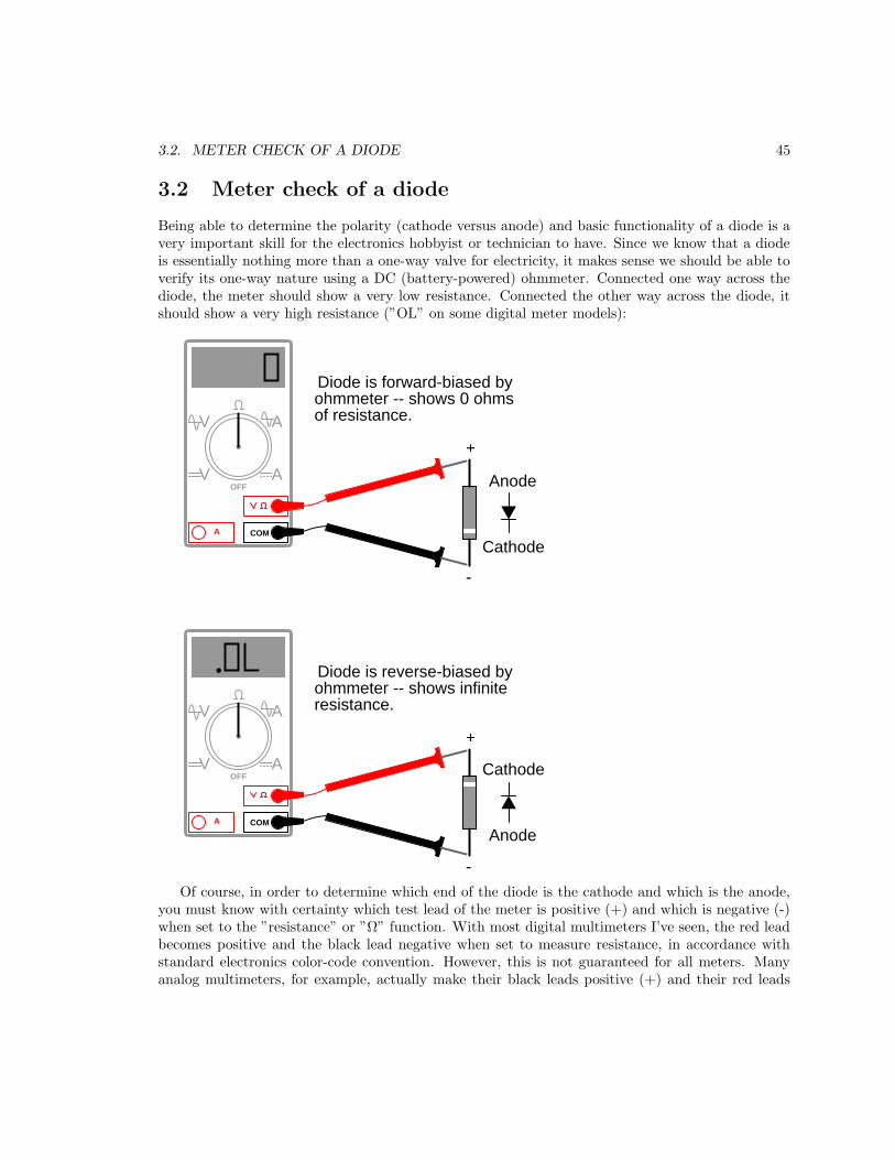
3.2. METER CHECK OF A DIODE 45
3.2 Meter check of a diode
Being able to determine the polarity (cathode versus anode) and basic functionality of a diode is avery important skill for the electronics hobbyist or technician to have. Since we know that a diodeis essentially nothing more than a one-way valve for electricity, it makes sense we should be able toverify its one-way nature using a DC (battery-powered) ohmmeter. Connected one way across thediode, the meter should show a very low resistance. Connected the other way across the diode, itshould show a very high resistance (”OL” on some digital meter models):
COMA
V
V A
AOFF Anode
Cathode
ohmmeter -- shows 0 ohmsDiode is forward-biased by
of resistance.
+
-
COMA
V
V A
AOFF
Anode
Cathode
+
-
Diode is reverse-biased byohmmeter -- shows infiniteresistance.
Of course, in order to determine which end of the diode is the cathode and which is the anode,you must know with certainty which test lead of the meter is positive (+) and which is negative (-)when set to the ”resistance” or ”Ω” function. With most digital multimeters I’ve seen, the red leadbecomes positive and the black lead negative when set to measure resistance, in accordance withstandard electronics color-code convention. However, this is not guaranteed for all meters. Manyanalog multimeters, for example, actually make their black leads positive (+) and their red leads

46 CHAPTER 3. DIODES AND RECTIFIERS
negative (-) when switched to the ”resistance” function, because it is easier to manufacture it thatway!
One problem with using an ohmmeter to check a diode is that the readings obtained only havequalitative value, not quantitative. In other words, an ohmmeter only tells you which way the diodeconducts; the low-value resistance indication obtained while conducting is useless. If an ohmmetershows a value of ”1.73 ohms” while forward-biasing a diode, that figure of 1.73 Ω doesn’t representany real-world quantity useful to us as technicians or circuit designers. It neither represents theforward voltage drop nor any ”bulk” resistance in the semiconductor material of the diode itself,but rather is a figure dependent upon both quantities and will vary substantially with the particularohmmeter used to take the reading.
For this reason, some digital multimeter manufacturers equip their meters with a special ”diodecheck” function which displays the actual forward voltage drop of the diode in volts, rather than a”resistance” figure in ohms. These meters work by forcing a small current through the diode andmeasuring the voltage dropped between the two test leads:
Anode
Cathode
Diode is forward-biased by
+
-
OFF
COMA
V A
V A
meter -- shows a forwardvoltage drop of 0.548 volts.
The forward voltage reading obtained with such a meter will typically be less than the ”normal”drop of 0.7 volts for silicon and 0.3 volts for germanium, because the current provided by the meteris of trivial proportions. If a multimeter with diode-check function isn’t available, or you would liketo measure a diode’s forward voltage drop at some non-trivial current, the following circuit may beconstructed using nothing but a battery, resistor, and a normal voltmeter:

3.2. METER CHECK OF A DIODE 47
+
-COMA
V
V A
AOFF +
-
Resistor
Battery
+V
-
Schematic diagramResistor sized to obtain diodecurrent of desired magnitude.
Connecting the diode backwards to this testing circuit will simply result in the voltmeter indi-cating the full voltage of the battery.
If this circuit were designed so as to provide a constant or nearly constant current throughthe diode despite changes in forward voltage drop, it could be used as the basis of a temperature-measurement instrument, the voltage measured across the diode being inversely proportional to diodejunction temperature. Of course, diode current should be kept to a minimum to avoid self-heating(the diode dissipating substantial amounts of heat energy), which would interfere with temperaturemeasurement.
Beware that some digital multimeters equipped with a ”diode check” function may output a verylow test voltage (less than 0.3 volts) when set to the regular ”resistance” (Ω) function: too low tofully collapse the depletion region of a PN junction. The philosophy here is that the ”diode check”function is to be used for testing semiconductor devices, and the ”resistance” function for anythingelse. By using a very low test voltage to measure resistance, it is easier for a technician to measurethe resistance of non-semiconductor components connected to semiconductor components, since thesemiconductor component junctions will not become forward-biased with such low voltages.
Consider the example of a resistor and diode connected in parallel, soldered in place on a printedcircuit board (PCB). Normally, one would have to unsolder the resistor from the circuit (disconnectit from all other components) before being able to measure its resistance, otherwise any parallel-connected components would affect the reading obtained. However, using a multimeter that outputsa very low test voltage to the probes in the ”resistance” function mode, the diode’s PN junctionwill not have enough voltage impressed across it to become forward-biased, and as such will passnegligible current. Consequently, the meter ”sees” the diode as an open (no continuity), and onlyregisters the resistor’s resistance:
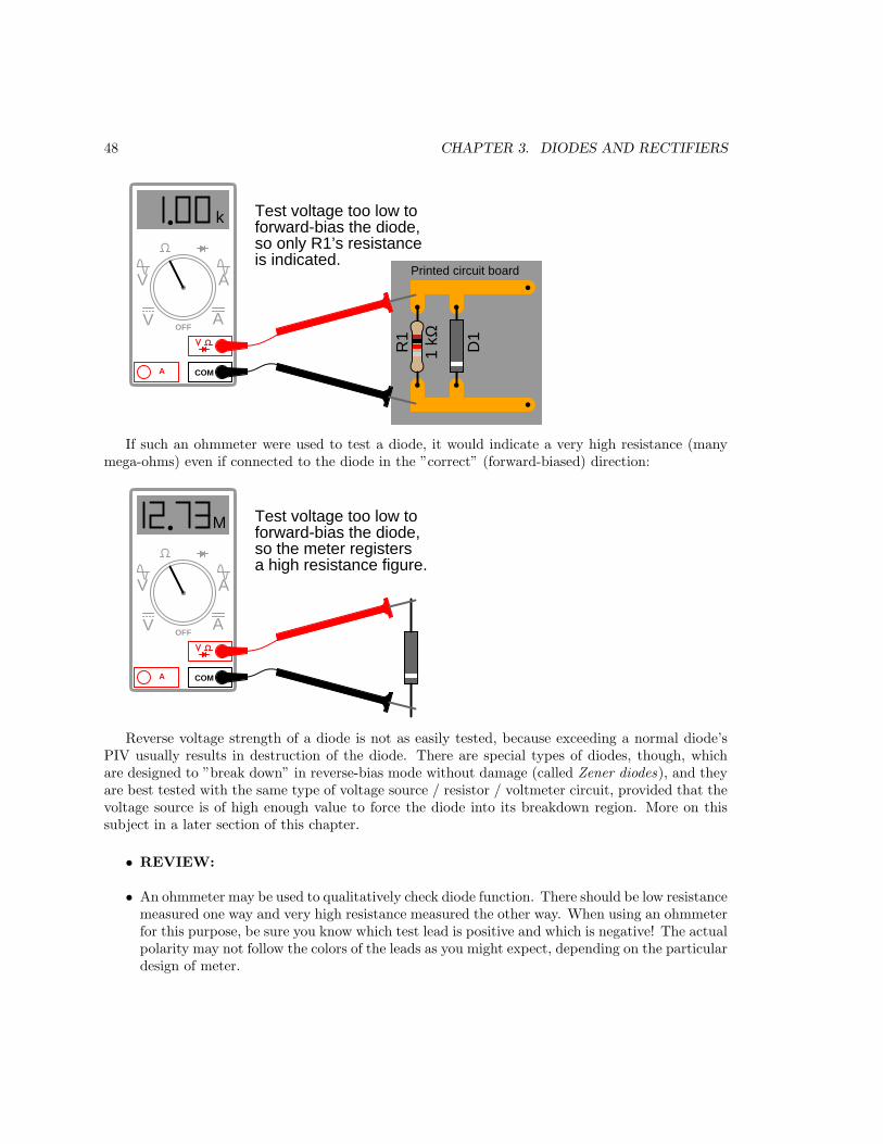
48 CHAPTER 3. DIODES AND RECTIFIERS
OFF
COMA
V A
V APrinted circuit board
R1
D1
1 kΩ
k Test voltage too low toforward-bias the diode,so only R1’s resistanceis indicated.
If such an ohmmeter were used to test a diode, it would indicate a very high resistance (manymega-ohms) even if connected to the diode in the ”correct” (forward-biased) direction:
OFF
COMA
V A
V A
Test voltage too low toforward-bias the diode,so the meter registers
M
a high resistance figure.
Reverse voltage strength of a diode is not as easily tested, because exceeding a normal diode’sPIV usually results in destruction of the diode. There are special types of diodes, though, whichare designed to ”break down” in reverse-bias mode without damage (called Zener diodes), and theyare best tested with the same type of voltage source / resistor / voltmeter circuit, provided that thevoltage source is of high enough value to force the diode into its breakdown region. More on thissubject in a later section of this chapter.
• REVIEW:
• An ohmmeter may be used to qualitatively check diode function. There should be low resistancemeasured one way and very high resistance measured the other way. When using an ohmmeterfor this purpose, be sure you know which test lead is positive and which is negative! The actualpolarity may not follow the colors of the leads as you might expect, depending on the particulardesign of meter.
3.3. DIODE RATINGS 49
• Some multimeters provide a ”diode check” function that displays the actual forward voltage ofthe diode when it’s conducting current. Such meters typically indicate a slightly lower forwardvoltage than what is ”nominal” for a diode, due to the very small amount of current usedduring the check.
3.3 Diode ratings
In addition to forward voltage drop (Vf ) and peak inverse voltage (PIV), there are many other ratingsof diodes important to circuit design and component selection. Semiconductor manufacturers providedetailed specifications on their products – diodes included – in publications known as datasheets.Datasheets for a wide variety of semiconductor components may be found in reference books and onthe internet. I personally prefer the internet as a source of component specifications because all thedata obtained from manufacturer websites are up-to-date.A typical diode datasheet will contain figures for the following parameters:Maximum repetitive reverse voltage = VRRM , the maximum amount of voltage the diode can
withstand in reverse-bias mode, in repeated pulses. Ideally, this figure would be infinite.Maximum DC reverse voltage = VR or VDC , the maximum amount of voltage the diode can
withstand in reverse-bias mode on a continual basis. Ideally, this figure would be infinite.Maximum forward voltage = VF , usually specified at the diode’s rated forward current. Ideally,
this figure would be zero: the diode providing no opposition whatsoever to forward current. Inreality, the forward voltage is described by the ”diode equation.”Maximum (average) forward current = IF (AV ), the maximum average amount of current the
diode is able to conduct in forward bias mode. This is fundamentally a thermal limitation: howmuch heat can the PN junction handle, given that dissipation power is equal to current (I) multipliedby voltage (V or E) and forward voltage is dependent upon both current and junction temperature.Ideally, this figure would be infinite.Maximum (peak or surge) forward current = IFSM or if(surge), the maximum peak amount of
current the diode is able to conduct in forward bias mode. Again, this rating is limited by thediode junction’s thermal capacity, and is usually much higher than the average current rating dueto thermal inertia (the fact that it takes a finite amount of time for the diode to reach maximumtemperature for a given current). Ideally, this figure would be infinite.Maximum total dissipation = PD, the amount of power (in watts) allowable for the diode to
dissipate, given the dissipation (P=IE) of diode current multiplied by diode voltage drop, and alsothe dissipation (P=I2R) of diode current squared multiplied by bulk resistance. Fundamentallylimited by the diode’s thermal capacity (ability to tolerate high temperatures).Operating junction temperature = TJ , the maximum allowable temperature for the diode’s PN
junction, usually given in degrees Celsius (oC). Heat is the ”Achilles’ heel” of semiconductor devices:they must be kept cool to function properly and give long service life.Storage temperature range = TSTG, the range of allowable temperatures for storing a diode (un-
powered). Sometimes given in conjunction with operating junction temperature (TJ ), because themaximum storage temperature and the maximum operating temperature ratings are often identi-cal. If anything, though, maximum storage temperature rating will be greater than the maximumoperating temperature rating.Thermal resistance = R(Θ), the temperature difference between junction and outside air (R(Θ)JA)
or between junction and leads (R(Θ)JL) for a given power dissipation. Expressed in units of degrees

50 CHAPTER 3. DIODES AND RECTIFIERS
Celsius per watt (oC/W). Ideally, this figure would be zero, meaning that the diode package wasa perfect thermal conductor and radiator, able to transfer all heat energy from the junction to theoutside air (or to the leads) with no difference in temperature across the thickness of the diodepackage. A high thermal resistance means that the diode will build up excessive temperature at thejunction (where it’s critical) despite best efforts at cooling the outside of the diode, and thus willlimit its maximum power dissipation.Maximum reverse current = IR, the amount of current through the diode in reverse-bias oper-
ation, with the maximum rated inverse voltage applied (VDC). Sometimes referred to as leakagecurrent. Ideally, this figure would be zero, as a perfect diode would block all current when reverse-biased. In reality, it is very small compared to the maximum forward current.Typical junction capacitance = CJ , the typical amount of capacitance intrinsic to the junction,
due to the depletion region acting as a dielectric separating the anode and cathode connections.This is usually a very small figure, measured in the range of picofarads (pF).Reverse recovery time = trr, the amount of time it takes for a diode to ”turn off” when the
voltage across it alternates from forward-bias to reverse-bias polarity. Ideally, this figure would bezero: the diode halting conduction immediately upon polarity reversal. For a typical rectifier diode,reverse recovery time is in the range of tens of microseconds; for a ”fast switching” diode, it mayonly be a few nanoseconds.Most of these parameters vary with temperature or other operating conditions, and so a single
figure fails to fully describe any given rating. Therefore, manufacturers provide graphs of componentratings plotted against other variables (such as temperature), so that the circuit designer has a betteridea of what the device is capable of.
3.4 Rectifier circuits
Now we come to the most popular application of the diode: rectification. Simply defined, rectificationis the conversion of alternating current (AC) to direct current (DC). This almost always involvesthe use of some device that only allows one-way flow of electrons. As we have seen, this is exactlywhat a semiconductor diode does. The simplest type of rectifier circuit is the half-wave rectifier, socalled because it only allows one half of an AC waveform to pass through to the load:
LoadAC
voltagesource
Half-wave rectifier circuit
+
-
For most power applications, half-wave rectification is insufficient for the task. The harmoniccontent of the rectifier’s output waveform is very large and consequently difficult to filter. Further-more, AC power source only works to supply power to the load once every half-cycle, meaning thatmuch of its capacity is unused. Half-wave rectification is, however, a very simple way to reduce

3.4. RECTIFIER CIRCUITS 51
power to a resistive load. Some two-position lamp dimmer switches apply full AC power to the lampfilament for ”full” brightness and then half-wave rectify it for a lesser light output:
ACvoltagesource
Bright
Dim
In the ”Dim” switch position, the incandescent lamp receives approximately one-half the powerit would normally receive operating on full-wave AC. Because the half-wave rectified power pulsesfar more rapidly than the filament has time to heat up and cool down, the lamp does not blink.Instead, its filament merely operates at a lesser temperature than normal, providing less light output.This principle of ”pulsing” power rapidly to a slow-responding load device in order to control theelectrical power sent to it is very common in the world of industrial electronics. Since the controllingdevice (the diode, in this case) is either fully conducting or fully nonconducting at any given time, itdissipates little heat energy while controlling load power, making this method of power control veryenergy-efficient. This circuit is perhaps the crudest possible method of pulsing power to a load, butit suffices as a proof-of-concept application.
If we need to rectify AC power so as to obtain the full use of both half-cycles of the sine wave,a different rectifier circuit configuration must be used. Such a circuit is called a full-wave rectifier.One type of full-wave rectifier, called the center-tap design, uses a transformer with a center-tappedsecondary winding and two diodes, like this:
LoadAC
voltagesource
Full-wave rectifier circuit
+
-
(center-tap design)
This circuit’s operation is easily understood one half-cycle at a time. Consider the first half-cycle,when the source voltage polarity is positive (+) on top and negative (-) on bottom. At this time,only the top diode is conducting; the bottom diode is blocking current, and the load ”sees” the firsthalf of the sine wave, positive on top and negative on bottom. Only the top half of the transformer’ssecondary winding carries current during this half-cycle:

52 CHAPTER 3. DIODES AND RECTIFIERS
+
-
+
-
+
-
During the next half-cycle, the AC polarity reverses. Now, the other diode and the other half ofthe transformer’s secondary winding carry current while the portions of the circuit formerly carryingcurrent during the last half-cycle sit idle. The load still ”sees” half of a sine wave, of the same polarityas before: positive on top and negative on bottom:
+
-+
-
+
-
One disadvantage of this full-wave rectifier design is the necessity of a transformer with a center-tapped secondary winding. If the circuit in question is one of high power, the size and expense ofa suitable transformer is significant. Consequently, the center-tap rectifier design is seen only inlow-power applications.Another, more popular full-wave rectifier design exists, and it is built around a four-diode bridge
configuration. For obvious reasons, this design is called a full-wave bridge:
Load
ACvoltagesource
Full-wave rectifier circuit
+
-
(bridge design)

3.4. RECTIFIER CIRCUITS 53
Current directions in the full-wave bridge rectifier circuit are as follows for each half-cycle of theAC waveform:
+
-
+
-
+
-
+
-
Remembering the proper layout of diodes in a full-wave bridge rectifier circuit can often befrustrating to the new student of electronics. I’ve found that an alternative representation of thiscircuit is easier both to remember and to comprehend. It’s the exact same circuit, except all diodesare drawn in a horizontal attitude, all ”pointing” the same direction:
Load
ACvoltagesource +
-
Full-wave bridge rectifier circuit(alternative layout)
One advantage of remembering this layout for a bridge rectifier circuit is that it expands easilyinto a polyphase version:

54 CHAPTER 3. DIODES AND RECTIFIERS
Load+
-
Three-phase, full-wavebridge rectifier circuit
3-phaseAC source
Each three-phase line connects between a pair of diodes: one to route power to the positive(+) side of the load, and the other to route power to the negative (-) side of the load. Polyphasesystems with more than three phases are easily accommodated into a bridge rectifier scheme. Takefor instance this six-phase bridge rectifier circuit:
Load+
-
bridge rectifier circuit
AC source
Six-phase, full-wave
6-phase
When polyphase AC is rectified, the phase-shifted pulses overlap each other to produce a DCoutput that is much ”smoother” (has less AC content) than that produced by the rectification ofsingle-phase AC. This is a decided advantage in high-power rectifier circuits, where the sheer physicalsize of filtering components would be prohibitive but low-noise DC power must be obtained. Thefollowing diagram shows the full-wave rectification of three-phase AC:

3.4. RECTIFIER CIRCUITS 55
1 2 3
TIME Resultant DC waveform
In any case of rectification – single-phase or polyphase – the amount of AC voltage mixed withthe rectifier’s DC output is called ripple voltage. In most cases, since ”pure” DC is the desiredgoal, ripple voltage is undesirable. If the power levels are not too great, filtering networks may beemployed to reduce the amount of ripple in the output voltage.
Sometimes, the method of rectification is referred to by counting the number of DC ”pulses”output for every 360o of electrical ”rotation.” A single-phase, half-wave rectifier circuit, then, wouldbe called a 1-pulse rectifier, because it produces a single pulse during the time of one complete cycle(360o) of the AC waveform. A single-phase, full-wave rectifier (regardless of design, center-tap orbridge) would be called a 2-pulse rectifier, because it outputs two pulses of DC during one AC cycle’sworth of time. A three-phase full-wave rectifier would be called a 6-pulse unit.
Modern electrical engineering convention further describes the function of a rectifier circuit byusing a three-field notation of phases, ways, and number of pulses. A single-phase, half-wave rectifiercircuit is given the somewhat cryptic designation of 1Ph1W1P (1 phase, 1 way, 1 pulse), meaningthat the AC supply voltage is single-phase, that current on each phase of the AC supply linesmoves in one direction (way) only, and that there is a single pulse of DC produced for every 360o
of electrical rotation. A single-phase, full-wave, center-tap rectifier circuit would be designated as1Ph1W2P in this notational system: 1 phase, 1 way or direction of current in each winding half, and2 pulses or output voltage per cycle. A single-phase, full-wave, bridge rectifier would be designatedas 1Ph2W2P: the same as for the center-tap design, except current can go both ways through theAC lines instead of just one way. The three-phase bridge rectifier circuit shown earlier would becalled a 3Ph2W6P rectifier.
Is it possible to obtain more pulses than twice the number of phases in a rectifier circuit? Theanswer to this question is yes: especially in polyphase circuits. Through the creative use of trans-formers, sets of full-wave rectifiers may be paralleled in such a way that more than six pulses of DCare produced for three phases of AC. A 30o phase shift is introduced from primary to secondary of athree-phase transformer when the winding configurations are not of the same type. In other words,a transformer connected either Y-∆ or ∆-Y will exhibit this 30o phase shift, while a transformerconnected Y-Y or ∆-∆ will not. This phenomenon may be exploited by having one transformerconnected Y-Y feed a bridge rectifier, and have another transformer connected Y-∆ feed a secondbridge rectifier, then parallel the DC outputs of both rectifiers. Since the ripple voltage waveformsof the two rectifiers’ outputs are phase-shifted 30o from one another, their superposition results inless ripple than either rectifier output considered separately: 12 pulses per 360o instead of just six:

56 CHAPTER 3. DIODES AND RECTIFIERS
+
-DC output
3-phaseAC input
Primary
Secondary
Secondary
3Ph2W12P rectifier circuit
• REVIEW:
• Rectification is the conversion of alternating current (AC) to direct current (DC).
• A half-wave rectifier is a circuit that allows only one half-cycle of the AC voltage waveform tobe applied to the load, resulting in one non-alternating polarity across it. The resulting DCdelivered to the load ”pulsates” significantly.
• A full-wave rectifier is a circuit that converts both half-cycles of the AC voltage waveform toan unbroken series of voltage pulses of the same polarity. The resulting DC delivered to theload doesn’t ”pulsate” as much.
• Polyphase alternating current, when rectified, gives a much ”smoother” DC waveform (lessripple voltage) than rectified single-phase AC.
3.5 Clipper circuits
3.6 Clamper circuits
3.7 Voltage multipliers
3.8 Inductor commutating circuits
A popular use of diodes is for the mitigation of inductive ”kickback:” the pulses of high voltageproduced when direct current through an inductor is interrupted. Take for example this simplecircuit:
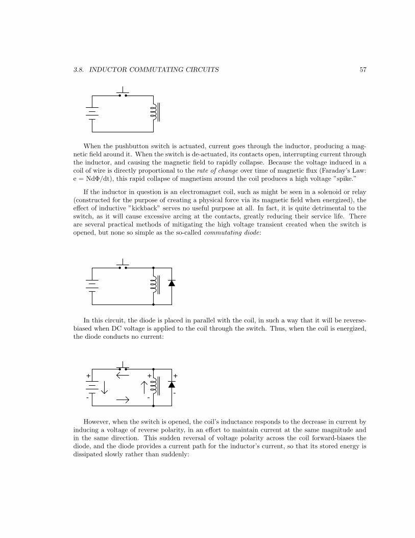
3.8. INDUCTOR COMMUTATING CIRCUITS 57
When the pushbutton switch is actuated, current goes through the inductor, producing a mag-netic field around it. When the switch is de-actuated, its contacts open, interrupting current throughthe inductor, and causing the magnetic field to rapidly collapse. Because the voltage induced in acoil of wire is directly proportional to the rate of change over time of magnetic flux (Faraday’s Law:e = NdΦ/dt), this rapid collapse of magnetism around the coil produces a high voltage ”spike.”
If the inductor in question is an electromagnet coil, such as might be seen in a solenoid or relay(constructed for the purpose of creating a physical force via its magnetic field when energized), theeffect of inductive ”kickback” serves no useful purpose at all. In fact, it is quite detrimental to theswitch, as it will cause excessive arcing at the contacts, greatly reducing their service life. Thereare several practical methods of mitigating the high voltage transient created when the switch isopened, but none so simple as the so-called commutating diode:
In this circuit, the diode is placed in parallel with the coil, in such a way that it will be reverse-biased when DC voltage is applied to the coil through the switch. Thus, when the coil is energized,the diode conducts no current:
+
-
+
-
+
-
However, when the switch is opened, the coil’s inductance responds to the decrease in current byinducing a voltage of reverse polarity, in an effort to maintain current at the same magnitude andin the same direction. This sudden reversal of voltage polarity across the coil forward-biases thediode, and the diode provides a current path for the inductor’s current, so that its stored energy isdissipated slowly rather than suddenly:

58 CHAPTER 3. DIODES AND RECTIFIERS
+
- +
-
+
-
As a result, the voltage induced in the coil by its collapsing magnetic field is quite low: merelythe forward voltage drop of the diode, rather than hundreds of volts as before. Thus, the switchcontacts experience a voltage drop equal to the battery voltage plus about 0.7 volts (if the diode issilicon) during this discharge time.In electronics parlance, commutation refers to the reversal of voltage polarity or current direction.
Thus, the purpose of a commutating diode is to act whenever voltage reverses polarity, in this case,the voltage induced by the inductor coil when current through it is interrupted by the switch. Aless formal term for a commutating diode is snubber, because it ”snubs” or ”squelches” the inductivekickback.A noteworthy disadvantage of this method is the extra time it imparts to the coil’s discharge.
Because the induced voltage is clamped to a very low value, its rate of magnetic flux change over timeis comparatively slow. Remember that Faraday’s Law describes the magnetic flux rate-of-change(dΦ/dt) as being proportional to the induced, instantaneous voltage (e or v). If the instantaneousvoltage is limited to some low figure, then the rate of change of magnetic flux over time will likewisebe limited to a low (slow) figure.If an electromagnet coil is ”snubbed” with a commutating diode, the magnetic field will dissipate
at a relatively slow rate compared to the original scenario (no diode) where the field disappearedalmost instantly upon switch release. The amount of time in question will most likely be less thanone second, but it will be measurably slower than without a commutating diode in place. This maybe an intolerable consequence if the coil is used to actuate an electromechanical relay, because therelay will possess a natural ”time delay” upon coil de-energization, and an unwanted delay of evena fraction of a second may wreak havoc in some circuits.Unfortunately, there is no way to eliminate the high-voltage transient of inductive kickback and
maintain fast de-magnetization of the coil: Faraday’s Law will not be violated. However, if slowde-magnetization is unacceptable, a compromise may be struck between transient voltage and timeby allowing the coil’s voltage to rise to some higher level (but not so high as without a commutatingdiode in place). The following schematic shows how this may be done:
A resistor placed in series with the commutating diode allows the coil’s induced voltage to rise to

3.9. ZENER DIODES 59
a level greater than the diode’s forward voltage drop, thus hastening the process of de-magnetization.This, of course, will place the switch contacts under greater stress, and so the resistor must be sizedto limit that transient voltage at an acceptable maximum level.
3.9 Zener diodes
If we connect a diode and resistor in series with a DC voltage source so that the diode is forward-biased, the voltage drop across the diode will remain fairly constant over a wide range of powersupply voltages:
≈ 0.7 V
According to the ”diode equation,” the current through a forward-biased PN junction is propor-tional to e raised to the power of the forward voltage drop. Because this is an exponential function,current rises quite rapidly for modest increases in voltage drop. Another way of considering this isto say that voltage dropped across a forward-biased diode changes little for large variations in diodecurrent. In the circuit shown above, diode current is limited by the voltage of the power supply, theseries resistor, and the diode’s voltage drop, which as we know doesn’t vary much from 0.7 volts.If the power supply voltage were to be increased, the resistor’s voltage drop would increase almostthe same amount, and the diode’s voltage drop just a little. Conversely, a decrease in power supplyvoltage would result in an almost equal decrease in resistor voltage drop, with just a little decreasein diode voltage drop. In a word, we could summarize this behavior by saying that the diode isregulating the voltage drop at approximately 0.7 volts.
Voltage regulation is a useful diode property to exploit. Suppose we were building some kind ofcircuit which could not tolerate variations in power supply voltage, but needed to be powered bya chemical battery, whose voltage changes over its lifetime. We could form a circuit as shown andconnect the circuit requiring steady voltage across the diode, where it would receive an unchanging0.7 volts.
This would certainly work, but most practical circuits of any kind require a power supply voltagein excess of 0.7 volts to properly function. One way we could increase our voltage regulation pointwould be to connect multiple diodes in series, so that their individual forward voltage drops of0.7 volts each would add to create a larger total. For instance, if we had ten diodes in series, theregulated voltage would be ten times 0.7, or 7 volts:

60 CHAPTER 3. DIODES AND RECTIFIERS
≈ 7.0 V
So long as the battery voltage never sagged below 7 volts, there would always be about 7 voltsdropped across the ten-diode ”stack.”
If larger regulated voltages are required, we could either use more diodes in series (an inelegantoption, in my opinion), or try a fundamentally different approach. We know that diode forwardvoltage is a fairly constant figure under a wide range of conditions, but so is reverse breakdownvoltage, and breakdown voltage is typically much, much greater than forward voltage. If we reversedthe polarity of the diode in our single-diode regulator circuit and increased the power supply voltageto the point where the diode ”broke down” (could no longer withstand the reverse-bias voltageimpressed across it), the diode would similarly regulate the voltage at that breakdown point, notallowing it to increase further:
150 V ≈ 100 V
≈ 50 V
Diode Vbreakdown = 100 V
Unfortunately, when normal rectifying diodes ”break down,” they usually do so destructively.However, it is possible to build a special type of diode that can handle breakdown without failingcompletely. This type of diode is called a zener diode, and its symbol looks like this:

3.9. ZENER DIODES 61
Zener diode
Anode
Cathode
When forward-biased, zener diodes behave much the same as standard rectifying diodes: theyhave a forward voltage drop which follows the ”diode equation” and is about 0.7 volts. In reverse-bias mode, they do not conduct until the applied voltage reaches or exceeds the so-called zenervoltage, at which point the diode is able to conduct substantial current, and in doing so will try tolimit the voltage dropped across it to that zener voltage point. So long as the power dissipated bythis reverse current does not exceed the diode’s thermal limits, the diode will not be harmed.
Zener diodes are manufactured with zener voltages ranging anywhere from a few volts to hundredsof volts. This zener voltage changes slightly with temperature, and like common carbon-compositionresistor values, may be anywhere from 5 percent to 10 percent in error from the manufacturer’sspecifications. However, this stability and accuracy is generally good enough for the zener diode tobe used as a voltage regulator device in common power supply circuit:
Diode Vzener = 12.6 V
≈ 12.6 V
Please take note of the zener diode’s orientation in the above circuit: the diode is reverse-biased,and intentionally so. If we had oriented the diode in the ”normal” way, so as to be forward-biased,it would only drop 0.7 volts, just like a regular rectifying diode. If we want to exploit this diode’sreverse breakdown properties, we must operate it in its reverse-bias mode. So long as the powersupply voltage remains above the zener voltage (12.6 volts, in this example), the voltage droppedacross the zener diode will remain at approximately 12.6 volts.
Like any semiconductor device, the zener diode is sensitive to temperature. Excessive tempera-ture will destroy a zener diode, and because it both drops voltage and conducts current, it producesits own heat in accordance with Joule’s Law (P=IE). Therefore, one must be careful to design theregulator circuit in such a way that the diode’s power dissipation rating is not exceeded. Interest-ingly enough, when zener diodes fail due to excessive power dissipation, they usually fail shortedrather than open. A diode failed in this manner is easy to detect: it drops almost zero voltage whenbiased either way, like a piece of wire.
Let’s examine a zener diode regulating circuit mathematically, determining all voltages, currents,and power dissipations. Taking the same form of circuit shown earlier, we’ll perform calculationsassuming a zener voltage of 12.6 volts, a power supply voltage of 45 volts, and a series resistor valueof 1000 Ω (we’ll regard the zener voltage to be exactly 12.6 volts so as to avoid having to qualify allfigures as ”approximate”):

62 CHAPTER 3. DIODES AND RECTIFIERS
Diode Vzener = 12.6 V
45 V
1 kΩ
12.6 V
If the zener diode’s voltage is 12.6 volts and the power supply’s voltage is 45 volts, there will be32.4 volts dropped across the resistor (45 volts - 12.6 volts = 32.4 volts). 32.4 volts dropped across1000 Ω gives 32.4 mA of current in the circuit:
45 V
1 kΩ
32.4 mA
32.4 mA
32.4 V
12.6 V
Power is calculated by multiplying current by voltage (P=IE), so we can calculate power dissi-pations for both the resistor and the zener diode quite easily:
Presistor = (32.4 mA)(32.4 V)
Pdiode = (32.4 mA)(12.6 V)
Presistor = 1.0498 W
Pdiode = 408.24 mW
A zener diode with a power rating of 0.5 watt would be adequate, as would a resistor rated for1.5 or 2 watts of dissipation.
If excessive power dissipation is detrimental, then why not design the circuit for the least amountof dissipation possible? Why not just size the resistor for a very high value of resistance, thus severelylimiting current and keeping power dissipation figures very low? Take this circuit, for example, witha 100 kΩ resistor instead of a 1 kΩ resistor. Note that both the power supply voltage and the diode’szener voltage are identical to the last example:

3.9. ZENER DIODES 63
45 V
32.4 V
12.6 V
100 kΩ
324 µA
324 µA
With only 1/100 of the current we had before (324 µA instead of 32.4 mA), both power dissipationfigures should be 100 times smaller:
Presistor = (324 µA)(32.4 V)
Presistor = 10.498 mW
Pdiode = (324 µA)(12.6 V)
Pdiode = 4.0824 mW
Seems ideal, doesn’t it? Less power dissipation means lower operating temperatures for both thediode and the resistor, and also less wasted energy in the system, right? A higher resistance valuedoes reduce power dissipation levels in the circuit, but it unfortunately introduces another problem.Remember that the purpose of a regulator circuit is to provide a stable voltage for another circuit.In other words, we’re eventually going to power something with 12.6 volts, and this something willhave a current draw of its own. Consider our first regulator circuit, this time with a 500 Ω loadconnected in parallel with the zener diode:
45 V
1 kΩ
32.4 mA
32.4 mA
32.4 V
12.6 VRload
500 Ω
25.2 mA
25.2 mA
7.2 mA
If 12.6 volts is maintained across a 500 Ω load, the load will draw 25.2 mA of current. In orderfor the 1 kΩ series ”dropping” resistor to drop 32.4 volts (reducing the power supply’s voltage of 45volts down to 12.6 across the zener), it still must conduct 32.4 mA of current. This leaves 7.2 mAof current through the zener diode.
Now consider our ”power-saving” regulator circuit with the 100 kΩ dropping resistor, deliveringpower to the same 500 Ω load. What it is supposed to do is maintain 12.6 volts across the load, justlike the last circuit. However, as we will see, it cannot accomplish this task:

64 CHAPTER 3. DIODES AND RECTIFIERS
45 VRload
500 Ω
100 kΩ
224 mV
44.776 V
447.76 µA
447.76 µA 447.76 µA
447.76 µA
0 µA
With the larger value of dropping resistor in place, there will only be about 224 mV of voltageacross the 500 Ω load, far less than the expected value of 12.6 volts! Why is this? If we actually had12.6 volts across the load, it would draw 25.2 mA of current, as before. This load current would haveto go through the series dropping resistor as it did before, but with a new (much larger!) droppingresistor in place, the voltage dropped across that resistor with 25.2 mA of current going through itwould be 2,520 volts! Since we obviously don’t have that much voltage supplied by the battery, thiscannot happen.
The situation is easier to comprehend if we temporarily remove the zener diode from the circuitand analyze the behavior of the two resistors alone:
45 VRload
500 Ω
100 kΩ
224 mV
44.776 V
447.76 µA
447.76 µA 447.76 µA
447.76 µA
Both the 100 kΩ dropping resistor and the 500 Ω load resistance are in series with each other,giving a total circuit resistance of 100.5 kΩ. With a total voltage of 45 volts and a total resistanceof 100.5 kΩ, Ohm’s Law (I=E/R) tells us that the current will be 447.76 µA. Figuring voltage dropsacross both resistors (E=IR), we arrive at 44.776 volts and 224 mV, respectively. If we were tore-install the zener diode at this point, it would ”see” 224 mV across it as well, being in parallelwith the load resistance. This is far below the zener breakdown voltage of the diode and so it willnot ”break down” and conduct current. For that matter, at this low voltage the diode wouldn’tconduct even if it were forward-biased! Thus, the diode ceases to regulate voltage, for it can do soonly when there is at least 12.6 volts dropped across to ”activate” it.
The analytical technique of removing a zener diode from a circuit and seeing whether or not thereis enough voltage present to make it conduct is a sound one. Just because a zener diode happens tobe connected in a circuit doesn’t guarantee that the full zener voltage will always be dropped acrossit! Remember that zener diodes work by limiting voltage to some maximum level; they cannot makeup for a lack of voltage.
In summary, any zener diode regulating circuit will function so long as the load’s resistance isequal to or greater than some minimum value. If the load resistance is too low, it will draw too much

3.9. ZENER DIODES 65
current, dropping too much voltage across the series dropping resistor, leaving insufficient voltageacross the zener diode to make it conduct. When the zener diode stops conducting current, it canno longer regulate voltage, and the load voltage will fall below the regulation point.
Our regulator circuit with the 100 kΩ dropping resistor must be good for some value of loadresistance, though. To find this acceptable load resistance value, we can use a table to calculateresistance in the two-resistor series circuit (no diode), inserting the known values of total voltageand dropping resistor resistance, and calculating for an expected load voltage of 12.6 volts:
E
I
R
Volts
Amps
Ohms
Rdropping Rload Total
100 k
4512.6
With 45 volts of total voltage and 12.6 volts across the load, we should have 32.4 volts acrossRdropping:
E
I
R
Volts
Amps
Ohms
Rdropping Rload Total
100 k
4512.632.4
With 32.4 volts across the dropping resistor, and 100 kΩ worth of resistance in it, the currentthrough it will be 324 µA:
E
I
R
Volts
Amps
Ohms
Rdropping Rload Total
100 k
4512.632.4
324 µ
Ohm’s Law
I = ER
Being a series circuit, the current is equal through all components at any given time:

66 CHAPTER 3. DIODES AND RECTIFIERS
E
I
R
Volts
Amps
Ohms
Rdropping Rload Total
100 k
4512.632.4
324 µ 324 µ 324 µ
Rule of series circuits:ITotal = I1 = I2 = . . . In
Calculating load resistance is now a simple matter of Ohm’s Law (R = E/I), giving us 38.889kΩ:
E
I
R
Volts
Amps
Ohms
Rdropping Rload Total
100 k
4512.632.4
324 µ 324 µ 324 µ38.889 k
Ohm’s Law
R = EI
Thus, if the load resistance is exactly 38.889 kΩ, there will be 12.6 volts across it, diode or nodiode. Any load resistance smaller than 38.889 kΩ will result in a load voltage less than 12.6 volts,diode or no diode. With the diode in place, the load voltage will be regulated to a maximum of 12.6volts for any load resistance greater than 38.889 kΩ.
With the original value of 1 kΩ for the dropping resistor, our regulator circuit was able toadequately regulate voltage even for a load resistance as low as 500 Ω. What we see is a tradeoffbetween power dissipation and acceptable load resistance. The higher-value dropping resistor gaveus less power dissipation, at the expense of raising the acceptable minimum load resistance value.If we wish to regulate voltage for low-value load resistances, the circuit must be prepared to handlehigher power dissipation.
Zener diodes regulate voltage by acting as complementary loads, drawing more or less current asnecessary to ensure a constant voltage drop across the load. This is analogous to regulating the speedof an automobile by braking rather than by varying the throttle position: not only is it wasteful,but the brakes must be built to handle all the engine’s power when the driving conditions don’tdemand it. Despite this fundamental inefficiency of design, zener diode regulator circuits are widelyemployed due to their sheer simplicity. In high-power applications where the inefficiencies wouldbe unacceptable, other voltage-regulating techniques are applied. But even then, small zener-basedcircuits are often used to provide a ”reference” voltage to drive a more efficient amplifier-type ofcircuit controlling the main power.
• REVIEW:

3.10. SPECIAL-PURPOSE DIODES 67
• Zener diodes are designed to be operated in reverse-bias mode, providing a relatively low,stable breakdown, or zener voltage at which they being to conduct substantial reverse current.
• A zener diode may function as a voltage regulator by acting as an accessory load, drawingmore current from the source if the voltage is too high, and less if it is too low.
3.10 Special-purpose diodes
3.10.1 Schottky diodes
Schottky diodes are constructed of a metal -to-N junction rather than a P-N semiconductor junction.Also known as hot-carrier diodes, Schottky diodes are characterized by fast switching times (lowreverse-recovery time), low forward voltage drop (typically 0.25 to 0.4 volts for a metal-siliconjunction), and low junction capacitance.
The schematic symbol for a Schottky diode is shown here:
Schottky diode
Anode
Cathode
In terms of forward voltage drop (VF ), reverse-recovery time (trr), and junction capacitance(CJ ), Schottky diodes are closer to ideal than the average ”rectifying” diode. This makes them wellsuited for high-frequency applications. Unfortunately, though, Schottky diodes typically have lowerforward current (IF ) and reverse voltage (VRRM and VDC) ratings than rectifying diodes and arethus unsuitable for applications involving substantial amounts of power.
Schottky diode technology finds broad application in high-speed computer circuits, where thefast switching time equates to high speed capability, and the low forward voltage drop equates toless power dissipation when conducting.
3.10.2 Tunnel diodes
Tunnel diodes exploit a strange quantum phenomenon called resonant tunneling to provide inter-esting forward-bias characteristics. When a small forward-bias voltage is applied across a tunneldiode, it begins to conduct current. As the voltage is increased, the current increases and reaches apeak value called the peak current (IP ). If the voltage is increased a little more, the current actuallybegins to decrease until it reaches a low point called the valley current (IV ). If the voltage is in-creased further yet, the current begins to increase again, this time without decreasing into another”valley.” Both the schematic symbol and a current/voltage plot for the tunnel diode are shown inthe following illustration:

68 CHAPTER 3. DIODES AND RECTIFIERS
Anode
Cathode
Tunnel diode
Forward voltage
Forwardcurrent
IP
IV
VP VV
The forward voltages necessary to drive a tunnel diode to its peak and valley currents are knownas peak voltage (VP ) and valley voltage (VV ), respectively. The region on the graph where currentis decreasing while applied voltage is increasing (between VP and VV on the horizontal scale) isknown as the region of negative resistance.
Tunnel diodes, also known as Esaki diodes in honor of their Japanese inventor Leo Esaki, areable to transition between peak and valley current levels very quickly, ”switching” between high andlow states of conduction much faster than even Schottky diodes. Tunnel diode characteristics arealso relatively unaffected by changes in temperature.
Unfortunately, tunnel diodes are not good rectifiers, as they have relatively high ”leakage” currentwhen reverse-biased. Consequently, they find application only in special circuits where their uniquetunnel effect has value. In order to exploit the tunnel effect, these diodes are maintained at a biasvoltage somewhere between the peak and valley voltage levels, always in a forward-biased polarity(anode positive, and cathode negative).
Perhaps the most common application of a tunnel diode is in simple high-frequency oscillatorcircuits, where they allow a DC voltage source to contribute power to an LC ”tank” circuit, thediode conducting when the voltage across it reaches the peak (tunnel) level and effectively insulatingat all other voltages.
3.10.3 Light-emitting diodes
Diodes, like all semiconductor devices, are governed by the principles described in quantum physics.One of these principles is the emission of specific-frequency radiant energy whenever electrons fallfrom a higher energy level to a lower energy level. This is the same principle at work in a neonlamp, the characteristic pink-orange glow of ionized neon due to the specific energy transitions of itselectrons in the midst of an electric current. The unique color of a neon lamp’s glow is due to the factthat it’s neon gas inside the tube, and not due to the particular amount of current through the tubeor voltage between the two electrodes. Neon gas glows pinkish-orange over a wide range of ionizingvoltages and currents. Each chemical element has its own ”signature” emission of radiant energywhen its electrons ”jump” between different, quantized energy levels. Hydrogen gas, for example,glows red when ionized; mercury vapor glows blue. This is what makes spectrographic identificationof elements possible.
Electrons flowing through a PN junction experience similar transitions in energy level, and emitradiant energy as they do so. The frequency of this radiant energy is determined by the crystal

3.10. SPECIAL-PURPOSE DIODES 69
structure of the semiconductor material, and the elements comprising it. Some semiconductorjunctions, composed of special chemical combinations, emit radiant energy within the spectrum ofvisible light as the electrons transition in energy levels. Simply put, these junctions glow whenforward biased. A diode intentionally designed to glow like a lamp is called a light-emitting diode,or LED.Diodes made from a combination of the elements gallium, arsenic, and phosphorus (called
gallium-arsenide-phosphide) glow bright red, and are some of the most common LEDs manufac-tured. By altering the chemical constituency of the PN junction, different colors may be obtained.Some of the currently available colors other than red are green, blue, and infra-red (invisible lightat a frequency lower than red). Other colors may be obtained by combining two or more primary-color (red, green, and blue) LEDs together in the same package, sharing the same optical lens. Forinstance, a yellow LED may be made by merging a red LED with a green LED.The schematic symbol for an LED is a regular diode shape inside of a circle, with two small
arrows pointing away (indicating emitted light):
Anode
Cathode
Light-emitting diode (LED)
This notation of having two small arrows pointing away from the device is common to theschematic symbols of all light-emitting semiconductor devices. Conversely, if a device is light-activated (meaning that incoming light stimulates it), then the symbol will have two small arrowspointing toward it. It is interesting to note, though, that LEDs are capable of acting as light-sensingdevices: they will generate a small voltage when exposed to light, much like a solar cell on a smallscale. This property can be gainfully applied in a variety of light-sensing circuits.Because LEDs are made of different chemical substances than normal rectifying diodes, their
forward voltage drops will be different. Typically, LEDs have much larger forward voltage dropsthan rectifying diodes, anywhere from about 1.6 volts to over 3 volts, depending on the color. Typicaloperating current for a standard-sized LED is around 20 mA. When operating an LED from a DCvoltage source greater than the LED’s forward voltage, a series-connected ”dropping” resistor mustbe included to prevent full source voltage from damaging the LED. Consider this example circuit:
6 V
Red LED,VF = 1.6 V typicalIF = 20 mA typical
Rdropping
220 Ω
With the LED dropping 1.6 volts, there will be 4.4 volts dropped across the resistor. Sizing theresistor for an LED current of 20 mA is as simple as taking its voltage drop (4.4 volts) and dividingby circuit current (20 mA), in accordance with Ohm’s Law (R=E/I). This gives us a figure of 220 Ω.Calculating power dissipation for this resistor, we take its voltage drop and multiply by its current(P=IE), and end up with 88 mW, well within the rating of a 1/8 watt resistor. Higher battery

70 CHAPTER 3. DIODES AND RECTIFIERS
voltages will require larger-value dropping resistors, and possibly higher-power rating resistors aswell. Consider this example for a supply voltage of 24 volts:
Red LED,VF = 1.6 V typicalIF = 20 mA typical
Rdropping
24 V1.12 kΩ
Here, the dropping resistor must be increased to a size of 1.12 kΩ in order to drop 22.4 voltsat 20 mA so that the LED still receives only 1.6 volts. This also makes for a higher resistor powerdissipation: 448 mW, nearly one-half a watt of power! Obviously, a resistor rated for 1/8 watt powerdissipation or even 1/4 watt dissipation will overheat if used here.Dropping resistor values need not be precise for LED circuits. Suppose we were to use a 1 kΩ
resistor instead of a 1.12 kΩ resistor in the circuit shown above. The result would be a slightlygreater circuit current and LED voltage drop, resulting in a brighter light from the LED and slightlyreduced service life. A dropping resistor with too much resistance (say, 1.5 kΩ instead of 1.12 kΩ)will result in less circuit current, less LED voltage, and a dimmer light. LEDs are quite tolerant ofvariation in applied power, so you need not strive for perfection in sizing the dropping resistor.Also because of their unique chemical makeup, LEDs have much, much lower peak-inverse voltage
(PIV) ratings than ordinary rectifying diodes. A typical LED might only be rated at 5 volts inreverse-bias mode. Therefore, when using alternating current to power an LED, you should connecta protective rectifying diode in series with the LED to prevent reverse breakdown every other half-cycle:
Red LED,VF = 1.6 V typicalIF = 20 mA typical
Rdropping
1.12 kΩ24 V
VR = 5 V maximum
rectifying diodeAs lamps, LEDs are superior to incandescent bulbs in many ways. First and foremost is effi-
ciency: LEDs output far more light power per watt than an incandescent lamp. This is a significantadvantage if the circuit in question is battery-powered, efficiency translating to longer battery life.Second is the fact that LEDs are far more reliable, having a much greater service life than an in-candescent lamp. This advantage is primarily due to the fact that LEDs are ”cold” devices: theyoperate at much cooler temperatures than an incandescent lamp with a white-hot metal filament,susceptible to breakage from mechanical and thermal shock. Third is the high speed at which LEDsmay be turned on and off. This advantage is also due to the ”cold” operation of LEDs: they don’thave to overcome thermal inertia in transitioning from off to on or vice versa. For this reason, LEDsare used to transmit digital (on/off) information as pulses of light, conducted in empty space orthrough fiber-optic cable, at very high rates of speed (millions of pulses per second).One major disadvantage of using LEDs as sources of illumination is their monochromatic (single-
color) emission. No one wants to read a book under the light of a red, green, or blue LED. However,
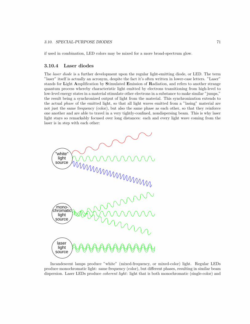
3.10. SPECIAL-PURPOSE DIODES 71
if used in combination, LED colors may be mixed for a more broad-spectrum glow.
3.10.4 Laser diodes
The laser diode is a further development upon the regular light-emitting diode, or LED. The term”laser” itself is actually an acronym, despite the fact it’s often written in lower-case letters. ”Laser”stands for Light Amplification by Stimulated Emission of Radiation, and refers to another strangequantum process whereby characteristic light emitted by electrons transitioning from high-level tolow-level energy states in a material stimulate other electrons in a substance to make similar ”jumps,”the result being a synchronized output of light from the material. This synchronization extends tothe actual phase of the emitted light, so that all light waves emitted from a ”lasing” material arenot just the same frequency (color), but also the same phase as each other, so that they reinforceone another and are able to travel in a very tightly-confined, nondispersing beam. This is why laserlight stays so remarkably focused over long distances: each and every light wave coming from thelaser is in step with each other:
"white"light
source
mono-chromatic
lightsource
laserlight
source
Incandescent lamps produce ”white” (mixed-frequency, or mixed-color) light. Regular LEDsproduce monochromatic light: same frequency (color), but different phases, resulting in similar beamdispersion. Laser LEDs produce coherent light : light that is both monochromatic (single-color) and

72 CHAPTER 3. DIODES AND RECTIFIERS
monophasic (single-phase), resulting in precise beam confinement.
Laser light finds wide application in the modern world: everything from surveying, where astraight and nondispersing light beam is very useful for precise sighting of measurement markers, tothe reading and writing of optical disks, where only the narrowness of a focused laser beam is ableto resolve the microscopic ”pits” in the disk’s surface comprising the binary 1’s and 0’s of digitalinformation.
Some laser diodes require special high-power ”pulsing” circuits to deliver large quantities ofvoltage and current in short bursts. Other laser diodes may be operated continuously at lower power.In the latter case, laser action occurs only within a certain range of diode current, necessitating someform of current-regulator circuit. As laser diodes age, their power requirements may change (morecurrent required for less output power), but it should be remembered that low-power laser diodes,like LEDs, are fairly long-lived devices, with typical service lives in the tens of thousands of hours.
3.10.5 Photodiodes
3.10.6 Varactor diodes
3.10.7 Constant-current diodes
A constant-current diode, also known as a current-limiting diode, or current-regulating diode, doesexactly what its name implies: it regulates current through it to some maximum level. If you tryto force more current through a constant-current diode than its current-regulation point, it simply”fights back” by dropping more voltage. If we were to build the following circuit and plot diodecurrent over diode current, we’d get a graph that rises normally at first and then levels off at thecurrent regulation point:
Rdropping
constant-currentdiode
Vdiode
Idiode
One interesting application for a constant-current diode is to automatically limit current throughan LED or laser diode over a wide range of power supply voltages, like this:

3.11. OTHER DIODE TECHNOLOGIES 73
constant-currentdiode
LED or laserdiode
Of course, the constant-current diode’s regulation point should be chosen to match the LED orlaser diode’s optimum forward current. This is especially important for the laser diode, not so muchfor the LED, as regular LEDs tend to be more tolerant of forward current variations.Another application is in the charging of small secondary-cell batteries, where a constant charging
current leads to very predictable charging times. Of course, large secondary-cell battery banksmight also benefit from constant-current charging, but constant-current diodes tend to be verysmall devices, limited to regulating currents in the milliamp range.
3.11 Other diode technologies
3.12 Contributors
Contributors to this chapter are listed in chronological order of their contributions, from most recentto first. See Appendix 2 (Contributor List) for dates and contact information.
Jered Wierzbicki (December 2002): Pointed out error in diode equation – Boltzmann’s con-stant shown incorrectly.

74 CHAPTER 3. DIODES AND RECTIFIERS

Chapter 4
BIPOLAR JUNCTIONTRANSISTORS
Contents
4.1 Introduction . . . . . . . . . . . . . . . . . . . . . . . . . . . . . . . . . . 75
4.2 The transistor as a switch . . . . . . . . . . . . . . . . . . . . . . . . . . 78
4.3 Meter check of a transistor . . . . . . . . . . . . . . . . . . . . . . . . . 81
4.4 Active mode operation . . . . . . . . . . . . . . . . . . . . . . . . . . . . 86
4.5 The common-emitter amplifier . . . . . . . . . . . . . . . . . . . . . . . 94
4.6 The common-collector amplifier . . . . . . . . . . . . . . . . . . . . . . . 110
4.7 The common-base amplifier . . . . . . . . . . . . . . . . . . . . . . . . . 119
4.8 Biasing techniques . . . . . . . . . . . . . . . . . . . . . . . . . . . . . . . 127
4.9 Input and output coupling . . . . . . . . . . . . . . . . . . . . . . . . . . 140
4.10 Feedback . . . . . . . . . . . . . . . . . . . . . . . . . . . . . . . . . . . . . 147
4.11 Amplifier impedances . . . . . . . . . . . . . . . . . . . . . . . . . . . . . 154
4.12 Current mirrors . . . . . . . . . . . . . . . . . . . . . . . . . . . . . . . . 155
4.13 Transistor ratings and packages . . . . . . . . . . . . . . . . . . . . . . . 158
4.14 BJT quirks . . . . . . . . . . . . . . . . . . . . . . . . . . . . . . . . . . . 159
*** INCOMPLETE ***
4.1 Introduction
The invention of the bipolar transistor in 1948 ushered in a revolution in electronics. Technicalfeats previously requiring relatively large, mechanically fragile, power-hungry vacuum tubes weresuddenly achievable with tiny, mechanically rugged, power-thrifty specks of crystalline silicon. Thisrevolution made possible the design and manufacture of lightweight, inexpensive electronic devicesthat we now take for granted. Understanding how transistors function is of paramount importanceto anyone interested in understanding modern electronics.
75

76 CHAPTER 4. BIPOLAR JUNCTION TRANSISTORS
My intent here is to focus as exclusively as possible on the practical function and application ofbipolar transistors, rather than to explore the quantum world of semiconductor theory. Discussionsof holes and electrons are better left to another chapter in my opinion. Here I want to explore howto use these components, not analyze their intimate internal details. I don’t mean to downplay theimportance of understanding semiconductor physics, but sometimes an intense focus on solid-statephysics detracts from understanding these devices’ functions on a component level. In taking thisapproach, however, I assume that the reader possesses a certain minimum knowledge of semiconduc-tors: the difference between ”P” and ”N” doped semiconductors, the functional characteristics of aPN (diode) junction, and the meanings of the terms ”reverse biased” and ”forward biased.” If theseconcepts are unclear to you, it is best to refer to earlier chapters in this book before proceeding withthis one.A bipolar transistor consists of a three-layer ”sandwich” of doped (extrinsic) semiconductor
materials, either P-N-P or N-P-N. Each layer forming the transistor has a specific name, and eachlayer is provided with a wire contact for connection to a circuit. Shown here are schematic symbolsand physical diagrams of these two transistor types:
schematic symbol
NP
P
emitter
base
collector
base
emitter
collector
PNP transistor
physical diagram
schematic symbol
NP
emitter
base
collector
base
emitter
collector
physical diagram
NPN transistor
N

4.1. INTRODUCTION 77
The only functional difference between a PNP transistor and an NPN transistor is the properbiasing (polarity) of the junctions when operating. For any given state of operation, the currentdirections and voltage polarities for each type of transistor are exactly opposite each other.Bipolar transistors work as current-controlled current regulators. In other words, they restrict
the amount of current that can go through them according to a smaller, controlling current. Themain current that is controlled goes from collector to emitter, or from emitter to collector, dependingon the type of transistor it is (PNP or NPN, respectively). The small current that controls the maincurrent goes from base to emitter, or from emitter to base, once again depending on the type oftransistor it is (PNP or NPN, respectively). According to the confusing standards of semiconductorsymbology, the arrow always points against the direction of electron flow:
CB
E
CB
E
= small, controlling current
= large, controlled current
Bipolar transistors are called bipolar because the main flow of electrons through them takes placein two types of semiconductor material: P and N, as the main current goes from emitter to collector(or vice versa). In other words, two types of charge carriers – electrons and holes – comprise thismain current through the transistor.As you can see, the controlling current and the controlled current always mesh together through
the emitter wire, and their electrons always flow against the direction of the transistor’s arrow. Thisis the first and foremost rule in the use of transistors: all currents must be going in the properdirections for the device to work as a current regulator. The small, controlling current is usuallyreferred to simply as the base current because it is the only current that goes through the basewire of the transistor. Conversely, the large, controlled current is referred to as the collector currentbecause it is the only current that goes through the collector wire. The emitter current is the sumof the base and collector currents, in compliance with Kirchhoff’s Current Law.If there is no current through the base of the transistor, it shuts off like an open switch and
prevents current through the collector. If there is a base current, then the transistor turns on like aclosed switch and allows a proportional amount of current through the collector. Collector currentis primarily limited by the base current, regardless of the amount of voltage available to push it.The next section will explore in more detail the use of bipolar transistors as switching elements.
• REVIEW:
• Bipolar transistors are so named because the controlled current must go through two types

78 CHAPTER 4. BIPOLAR JUNCTION TRANSISTORS
of semiconductor material: P and N. The current consists of both electron and hole flow, indifferent parts of the transistor.
• Bipolar transistors consist of either a P-N-P or an N-P-N semiconductor ”sandwich” structure.
• The three leads of a bipolar transistor are called the Emitter, Base, and Collector.
• Transistors function as current regulators by allowing a small current to control a larger current.The amount of current allowed between collector and emitter is primarily determined by theamount of current moving between base and emitter.
• In order for a transistor to properly function as a current regulator, the controlling (base)current and the controlled (collector) currents must be going in the proper directions: meshingadditively at the emitter and going against the emitter arrow symbol.
4.2 The transistor as a switch
Because a transistor’s collector current is proportionally limited by its base current, it can be used asa sort of current-controlled switch. A relatively small flow of electrons sent through the base of thetransistor has the ability to exert control over a much larger flow of electrons through the collector.
Suppose we had a lamp that we wanted to turn on and off by means of a switch. Such a circuitwould be extremely simple:
switch
For the sake of illustration, let’s insert a transistor in place of the switch to show how it cancontrol the flow of electrons through the lamp. Remember that the controlled current through atransistor must go between collector and emitter. Since it’s the current through the lamp that wewant to control, we must position the collector and emitter of our transistor where the two contactsof the switch are now. We must also make sure that the lamp’s current will move against thedirection of the emitter arrow symbol to ensure that the transistor’s junction bias will be correct:
transistorNPN
In this example I happened to choose an NPN transistor. A PNP transistor could also have beenchosen for the job, and its application would look like this:

4.2. THE TRANSISTOR AS A SWITCH 79
transistorPNP
The choice between NPN and PNP is really arbitrary. All that matters is that the proper currentdirections are maintained for the sake of correct junction biasing (electron flow going against thetransistor symbol’s arrow).Going back to the NPN transistor in our example circuit, we are faced with the need to add
something more so that we can have base current. Without a connection to the base wire of thetransistor, base current will be zero, and the transistor cannot turn on, resulting in a lamp that isalways off. Remember that for an NPN transistor, base current must consist of electrons flowingfrom emitter to base (against the emitter arrow symbol, just like the lamp current). Perhaps thesimplest thing to do would be to connect a switch between the base and collector wires of thetransistor like this:
switch
If the switch is open, the base wire of the transistor will be left ”floating” (not connected toanything) and there will be no current through it. In this state, the transistor is said to be cutoff.If the switch is closed, however, electrons will be able to flow from the emitter through to the baseof the transistor, through the switch and up to the left side of the lamp, back to the positive side ofthe battery. This base current will enable a much larger flow of electrons from the emitter throughto the collector, thus lighting up the lamp. In this state of maximum circuit current, the transistoris said to be saturated.
switch
Of course, it may seem pointless to use a transistor in this capacity to control the lamp. Afterall, we’re still using a switch in the circuit, aren’t we? If we’re still using a switch to control thelamp – if only indirectly – then what’s the point of having a transistor to control the current? Whynot just go back to our original circuit and use the switch directly to control the lamp current?There are a couple of points to be made here, actually. First is the fact that when used in
this manner, the switch contacts need only handle what little base current is necessary to turnthe transistor on, while the transistor itself handles the majority of the lamp’s current. This may

80 CHAPTER 4. BIPOLAR JUNCTION TRANSISTORS
be an important advantage if the switch has a low current rating: a small switch may be usedto control a relatively high-current load. Perhaps more importantly, though, is the fact that thecurrent-controlling behavior of the transistor enables us to use something completely different toturn the lamp on or off. Consider this example, where a solar cell is used to control the transistor,which in turn controls the lamp:
solarcell
Or, we could use a thermocouple to provide the necessary base current to turn the transistor on:
+-
thermocouple
source ofheat
Even a microphone of sufficient voltage and current output could be used to turn the transistoron, provided its output is rectified from AC to DC so that the emitter-base PN junction within thetransistor will always be forward-biased:
microphone
source ofsound
The point should be quite apparent by now: any sufficient source of DC current may be used toturn the transistor on, and that source of current need only be a fraction of the amount of currentneeded to energize the lamp. Here we see the transistor functioning not only as a switch, but asa true amplifier : using a relatively low-power signal to control a relatively large amount of power.Please note that the actual power for lighting up the lamp comes from the battery to the right ofthe schematic. It is not as though the small signal current from the solar cell, thermocouple, or
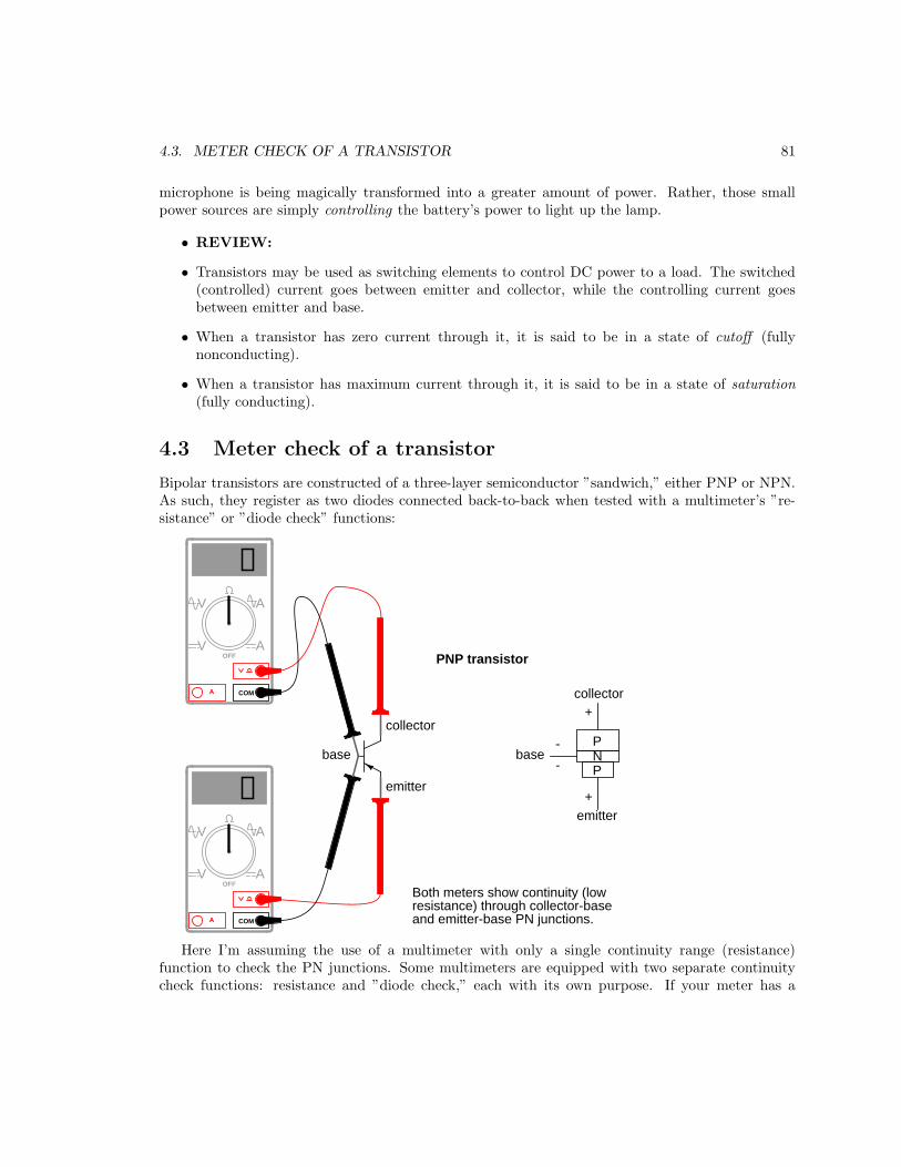
4.3. METER CHECK OF A TRANSISTOR 81
microphone is being magically transformed into a greater amount of power. Rather, those smallpower sources are simply controlling the battery’s power to light up the lamp.
• REVIEW:
• Transistors may be used as switching elements to control DC power to a load. The switched(controlled) current goes between emitter and collector, while the controlling current goesbetween emitter and base.
• When a transistor has zero current through it, it is said to be in a state of cutoff (fullynonconducting).
• When a transistor has maximum current through it, it is said to be in a state of saturation(fully conducting).
4.3 Meter check of a transistor
Bipolar transistors are constructed of a three-layer semiconductor ”sandwich,” either PNP or NPN.As such, they register as two diodes connected back-to-back when tested with a multimeter’s ”re-sistance” or ”diode check” functions:
NP
P
emitter
base
collector
base
emitter
collector
PNP transistor
COMA
V
V A
AOFF
COMA
V
V A
AOFF
+
-
+
-
Both meters show continuity (lowresistance) through collector-baseand emitter-base PN junctions.
Here I’m assuming the use of a multimeter with only a single continuity range (resistance)function to check the PN junctions. Some multimeters are equipped with two separate continuitycheck functions: resistance and ”diode check,” each with its own purpose. If your meter has a
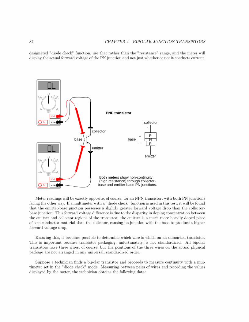
82 CHAPTER 4. BIPOLAR JUNCTION TRANSISTORS
designated ”diode check” function, use that rather than the ”resistance” range, and the meter willdisplay the actual forward voltage of the PN junction and not just whether or not it conducts current.
NP
P
emitter
base
collector
base
emitter
collector
PNP transistor
COMA
V
V A
AOFF
COMA
V
V A
AOFF
+
-
+
-
Both meters show non-continuity(high resistance) through collector-
base and emitter-base PN junctions.
Meter readings will be exactly opposite, of course, for an NPN transistor, with both PN junctionsfacing the other way. If a multimeter with a ”diode check” function is used in this test, it will be foundthat the emitter-base junction possesses a slightly greater forward voltage drop than the collector-base junction. This forward voltage difference is due to the disparity in doping concentration betweenthe emitter and collector regions of the transistor: the emitter is a much more heavily doped pieceof semiconductor material than the collector, causing its junction with the base to produce a higherforward voltage drop.
Knowing this, it becomes possible to determine which wire is which on an unmarked transistor.This is important because transistor packaging, unfortunately, is not standardized. All bipolartransistors have three wires, of course, but the positions of the three wires on the actual physicalpackage are not arranged in any universal, standardized order.
Suppose a technician finds a bipolar transistor and proceeds to measure continuity with a mul-timeter set in the ”diode check” mode. Measuring between pairs of wires and recording the valuesdisplayed by the meter, the technician obtains the following data:

4.3. METER CHECK OF A TRANSISTOR 83
1
2 3
Unknown bipolar transistor
Which wires are emitter,base, and collector?
• Meter touching wire 1 (+) and 2 (-): ”OL”
• Meter touching wire 1 (-) and 2 (+): ”OL”
• Meter touching wire 1 (+) and 3 (-): 0.655 volts
• Meter touching wire 1 (-) and 3 (+): ”OL”
• Meter touching wire 2 (+) and 3 (-): 0.621 volts
• Meter touching wire 2 (-) and 3 (+): ”OL”
The only combinations of test points giving conducting meter readings are wires 1 and 3 (redtest lead on 1 and black test lead on 3), and wires 2 and 3 (red test lead on 2 and black test lead on3). These two readings must indicate forward biasing of the emitter-to-base junction (0.655 volts)and the collector-to-base junction (0.621 volts).Now we look for the one wire common to both sets of conductive readings. It must be the base
connection of the transistor, because the base is the only layer of the three-layer device common toboth sets of PN junctions (emitter-base and collector-base). In this example, that wire is number3, being common to both the 1-3 and the 2-3 test point combinations. In both those sets of meterreadings, the black (-) meter test lead was touching wire 3, which tells us that the base of thistransistor is made of N-type semiconductor material (black = negative). Thus, the transistor is anPNP type with base on wire 3, emitter on wire 1 and collector on wire 2:
1
2 3Base
Emitter
Collector

84 CHAPTER 4. BIPOLAR JUNCTION TRANSISTORS
Please note that the base wire in this example is not the middle lead of the transistor, as onemight expect from the three-layer ”sandwich” model of a bipolar transistor. This is quite oftenthe case, and tends to confuse new students of electronics. The only way to be sure which lead iswhich is by a meter check, or by referencing the manufacturer’s ”data sheet” documentation on thatparticular part number of transistor.
Knowing that a bipolar transistor behaves as two back-to-back diodes when tested with a con-ductivity meter is helpful for identifying an unknown transistor purely by meter readings. It is alsohelpful for a quick functional check of the transistor. If the technician were to measure continuityin any more than two or any less than two of the six test lead combinations, he or she would imme-diately know that the transistor was defective (or else that it wasn’t a bipolar transistor but rathersomething else – a distinct possibility if no part numbers can be referenced for sure identification!).However, the ”two diode” model of the transistor fails to explain how or why it acts as an amplifyingdevice.
To better illustrate this paradox, let’s examine one of the transistor switch circuits using thephysical diagram rather than the schematic symbol to represent the transistor. This way the twoPN junctions will be easier to see:
NP
emitterbasecollector
N
solarcell
A grey-colored diagonal arrow shows the direction of electron flow through the emitter-basejunction. This part makes sense, since the electrons are flowing from the N-type emitter to the P-type base: the junction is obviously forward-biased. However, the base-collector junction is anothermatter entirely. Notice how the grey-colored thick arrow is pointing in the direction of electronflow (upwards) from base to collector. With the base made of P-type material and the collectorof N-type material, this direction of electron flow is clearly backwards to the direction normallyassociated with a PN junction! A normal PN junction wouldn’t permit this ”backward” direction offlow, at least not without offering significant opposition. However, when the transistor is saturated,there is very little opposition to electrons all the way from emitter to collector, as evidenced by thelamp’s illumination!
Clearly then, something is going on here that defies the simple ”two-diode” explanatory modelof the bipolar transistor. When I was first learning about transistor operation, I tried to constructmy own transistor from two back-to-back diodes, like this:
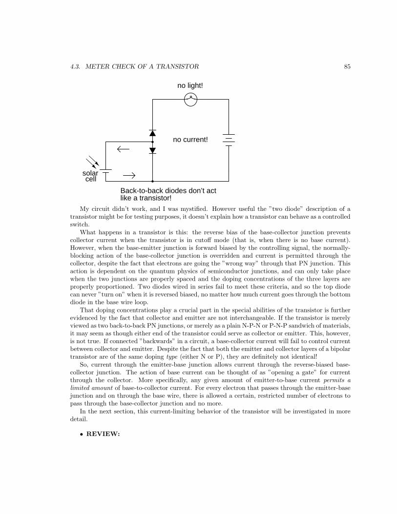
4.3. METER CHECK OF A TRANSISTOR 85
solarcell
no light!
no current!
Back-to-back diodes don’t actlike a transistor!
My circuit didn’t work, and I was mystified. However useful the ”two diode” description of atransistor might be for testing purposes, it doesn’t explain how a transistor can behave as a controlledswitch.What happens in a transistor is this: the reverse bias of the base-collector junction prevents
collector current when the transistor is in cutoff mode (that is, when there is no base current).However, when the base-emitter junction is forward biased by the controlling signal, the normally-blocking action of the base-collector junction is overridden and current is permitted through thecollector, despite the fact that electrons are going the ”wrong way” through that PN junction. Thisaction is dependent on the quantum physics of semiconductor junctions, and can only take placewhen the two junctions are properly spaced and the doping concentrations of the three layers areproperly proportioned. Two diodes wired in series fail to meet these criteria, and so the top diodecan never ”turn on” when it is reversed biased, no matter how much current goes through the bottomdiode in the base wire loop.That doping concentrations play a crucial part in the special abilities of the transistor is further
evidenced by the fact that collector and emitter are not interchangeable. If the transistor is merelyviewed as two back-to-back PN junctions, or merely as a plain N-P-N or P-N-P sandwich of materials,it may seem as though either end of the transistor could serve as collector or emitter. This, however,is not true. If connected ”backwards” in a circuit, a base-collector current will fail to control currentbetween collector and emitter. Despite the fact that both the emitter and collector layers of a bipolartransistor are of the same doping type (either N or P), they are definitely not identical!So, current through the emitter-base junction allows current through the reverse-biased base-
collector junction. The action of base current can be thought of as ”opening a gate” for currentthrough the collector. More specifically, any given amount of emitter-to-base current permits alimited amount of base-to-collector current. For every electron that passes through the emitter-basejunction and on through the base wire, there is allowed a certain, restricted number of electrons topass through the base-collector junction and no more.In the next section, this current-limiting behavior of the transistor will be investigated in more
detail.
• REVIEW:

86 CHAPTER 4. BIPOLAR JUNCTION TRANSISTORS
• Tested with a multimeter in the ”resistance” or ”diode check” modes, a transistor behaves liketwo back-to-back PN (diode) junctions.
• The emitter-base PN junction has a slightly greater forward voltage drop than the collector-base PN junction, due to more concentrated doping of the emitter semiconductor layer.
• The reverse-biased base-collector junction normally blocks any current from going through thetransistor between emitter and collector. However, that junction begins to conduct if currentis drawn through the base wire. Base current can be thought of as ”opening a gate” for acertain, limited amount of current through the collector.
4.4 Active mode operation
When a transistor is in the fully-off state (like an open switch), it is said to be cutoff. Conversely,when it is fully conductive between emitter and collector (passing as much current through thecollector as the collector power supply and load will allow), it is said to be saturated. These are thetwo modes of operation explored thus far in using the transistor as a switch.
However, bipolar transistors don’t have to be restricted to these two extreme modes of operation.As we learned in the previous section, base current ”opens a gate” for a limited amount of currentthrough the collector. If this limit for the controlled current is greater than zero but less than themaximum allowed by the power supply and load circuit, the transistor will ”throttle” the collectorcurrent in a mode somewhere between cutoff and saturation. This mode of operation is called theactive mode.
An automotive analogy for transistor operation is as follows: cutoff is the condition where thereis no motive force generated by the mechanical parts of the car to make it move. In cutoff mode, thebrake is engaged (zero base current), preventing motion (collector current). Active mode is whenthe automobile is cruising at a constant, controlled speed (constant, controlled collector current) asdictated by the driver. Saturation is when the automobile is driving up a steep hill that prevents itfrom going as fast as the driver would wish. In other words, a ”saturated” automobile is one wherethe accelerator pedal is pushed all the way down (base current calling for more collector currentthan can be provided by the power supply/load circuit).
I’ll set up a circuit for SPICE simulation to demonstrate what happens when a transistor is inits active mode of operation:

4.4. ACTIVE MODE OPERATION 87
V1
I1
Q1
Vammeter
0 V
1
0 0 0
2 3
Current source
”Q” is the standard letter designation for a transistor in a schematic diagram, just as ”R” is forresistor and ”C” is for capacitor. In this circuit, we have an NPN transistor powered by a battery(V1) and controlled by current through a current source (I1). A current source is a device thatoutputs a specific amount of current, generating as much or as little voltage as necessary acrossits terminals to ensure that exact amount of current through it. Current sources are notoriouslydifficult to find in nature (unlike voltage sources, which by contrast attempt to maintain a constantvoltage, outputting as much or as little current in the fulfillment of that task), but can be simulatedwith a small collection of electronic components. As we are about to see, transistors themselves tendto mimic the constant-current behavior of a current source in their ability to regulate current at afixed value.
In the SPICE simulation, I’ll set the current source at a constant value of 20 µA, then vary thevoltage source (V1) over a range of 0 to 2 volts and monitor how much current goes through it.The ”dummy” battery (Vammeter) with its output of 0 volts serves merely to provide SPICE witha circuit element for current measurement.
bipolar transistor simulation
i1 0 1 dc 20u
q1 2 1 0 mod1
vammeter 3 2 dc 0
v1 3 0 dc
.model mod1 npn
.dc v1 0 2 0.05
.plot dc i(vammeter)
.end
type npn
is 1.00E-16
bf 100.000
nf 1.000
br 1.000
nr 1.000
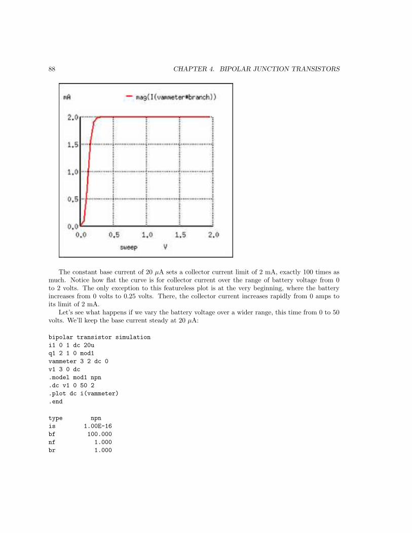
88 CHAPTER 4. BIPOLAR JUNCTION TRANSISTORS
The constant base current of 20 µA sets a collector current limit of 2 mA, exactly 100 times asmuch. Notice how flat the curve is for collector current over the range of battery voltage from 0to 2 volts. The only exception to this featureless plot is at the very beginning, where the batteryincreases from 0 volts to 0.25 volts. There, the collector current increases rapidly from 0 amps toits limit of 2 mA.Let’s see what happens if we vary the battery voltage over a wider range, this time from 0 to 50
volts. We’ll keep the base current steady at 20 µA:
bipolar transistor simulation
i1 0 1 dc 20u
q1 2 1 0 mod1
vammeter 3 2 dc 0
v1 3 0 dc
.model mod1 npn
.dc v1 0 50 2
.plot dc i(vammeter)
.end
type npn
is 1.00E-16
bf 100.000
nf 1.000
br 1.000

4.4. ACTIVE MODE OPERATION 89
nr 1.000
Same result! The collector current holds absolutely steady at 2 mA despite the fact that thebattery (v1) voltage varies all the way from 0 to 50 volts. It would appear from our simulationthat collector-to-emitter voltage has little effect over collector current, except at very low levels (justabove 0 volts). The transistor is acting as a current regulator, allowing exactly 2 mA through thecollector and no more.Now let’s see what happens if we increase the controlling (I1) current from 20 µA to 75 µA, once
again sweeping the battery (V1) voltage from 0 to 50 volts and graphing the collector current:
bipolar transistor simulation
i1 0 1 dc 75u
q1 2 1 0 mod1
vammeter 3 2 dc 0
v1 3 0 dc
.model mod1 npn
.dc v1 0 50 2
.plot dc i(vammeter)
.end
type npn
is 1.00E-16
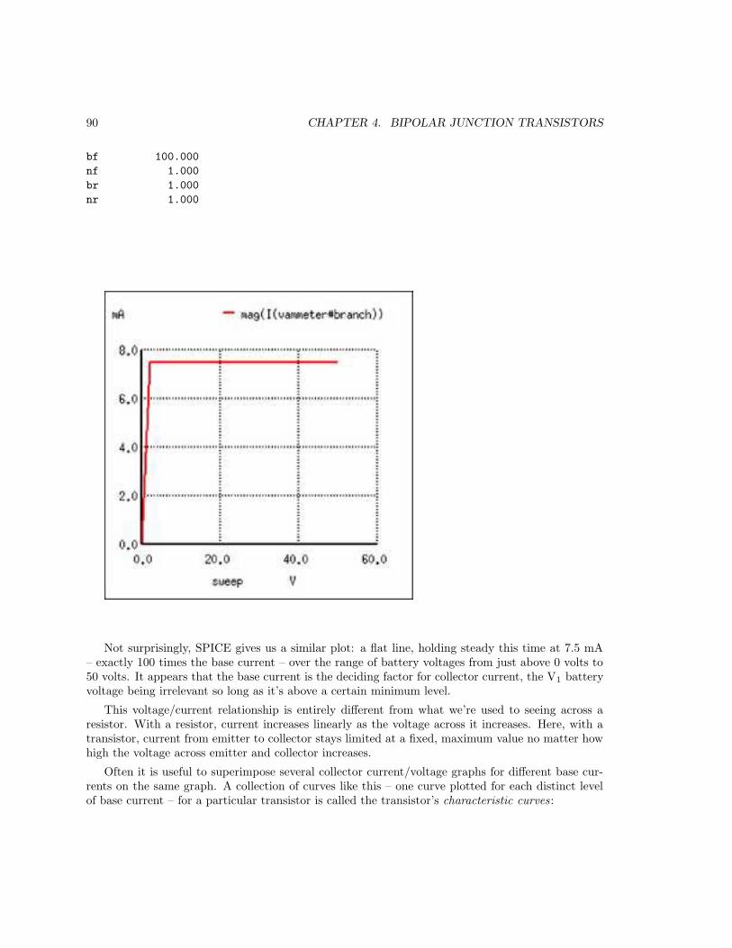
90 CHAPTER 4. BIPOLAR JUNCTION TRANSISTORS
bf 100.000
nf 1.000
br 1.000
nr 1.000
Not surprisingly, SPICE gives us a similar plot: a flat line, holding steady this time at 7.5 mA– exactly 100 times the base current – over the range of battery voltages from just above 0 volts to50 volts. It appears that the base current is the deciding factor for collector current, the V1 batteryvoltage being irrelevant so long as it’s above a certain minimum level.
This voltage/current relationship is entirely different from what we’re used to seeing across aresistor. With a resistor, current increases linearly as the voltage across it increases. Here, with atransistor, current from emitter to collector stays limited at a fixed, maximum value no matter howhigh the voltage across emitter and collector increases.
Often it is useful to superimpose several collector current/voltage graphs for different base cur-rents on the same graph. A collection of curves like this – one curve plotted for each distinct levelof base current – for a particular transistor is called the transistor’s characteristic curves:

4.4. ACTIVE MODE OPERATION 91
Icollector
Ecollector-to-emitter
Ibase = 75 µA
Ibase = 40 µA
Ibase = 20 µA
Ibase = 5 µA
(mA)
0 1 2 3 4 9 105 6 7 8 11 12 13 14
0
1
2
3
4
5
6
7
8
9
(V)
Each curve on the graph reflects the collector current of the transistor, plotted over a range ofcollector-to-emitter voltages, for a given amount of base current. Since a transistor tends to act asa current regulator, limiting collector current to a proportion set by the base current, it is usefulto express this proportion as a standard transistor performance measure. Specifically, the ratio ofcollector current to base current is known as the Beta ratio (symbolized by the Greek letter β):
β = Icollector
Ibase
β is also known as hfe
Sometimes the β ratio is designated as ”hfe,” a label used in a branch of mathematical semicon-ductor analysis known as ”hybrid parameters” which strives to achieve very precise predictions oftransistor performance with detailed equations. Hybrid parameter variables are many, but they areall labeled with the general letter ”h” and a specific subscript. The variable ”hfe” is just another(standardized) way of expressing the ratio of collector current to base current, and is interchangeablewith ”β.” Like all ratios, β is unitless.
β for any transistor is determined by its design: it cannot be altered after manufacture. However,there are so many physical variables impacting β that it is rare to have two transistors of the samedesign exactly match. If a circuit design relies on equal β ratios between multiple transistors,”matched sets” of transistors may be purchased at extra cost. However, it is generally consideredbad design practice to engineer circuits with such dependencies.
It would be nice if the β of a transistor remained stable for all operating conditions, but thisis not true in real life. For an actual transistor, the β ratio may vary by a factor of over 3 withinits operating current limits. For example, a transistor with advertised β of 50 may actually testwith Ic/Ib ratios as low as 30 and as high as 100, depending on the amount of collector current,the transistor’s temperature, and frequency of amplified signal, among other factors. For tutorialpurposes it is adequate to assume a constant β for any given transistor (which is what SPICE tends

92 CHAPTER 4. BIPOLAR JUNCTION TRANSISTORS
to do in a simulation), but just realize that real life is not that simple!
Sometimes it is helpful for comprehension to ”model” complex electronic components with acollection of simpler, better-understood components. The following is a popular model shown inmany introductory electronics texts:
NPN diode-rheostat model
B
C
E
C
E
B
This model casts the transistor as a combination of diode and rheostat (variable resistor). Currentthrough the base-emitter diode controls the resistance of the collector-emitter rheostat (as impliedby the dashed line connecting the two components), thus controlling collector current. An NPNtransistor is modeled in the figure shown, but a PNP transistor would be only slightly different(only the base-emitter diode would be reversed). This model succeeds in illustrating the basicconcept of transistor amplification: how the base current signal can exert control over the collectorcurrent. However, I personally don’t like this model because it tends to miscommunicate the notionof a set amount of collector-emitter resistance for a given amount of base current. If this were true,the transistor wouldn’t regulate collector current at all like the characteristic curves show. Insteadof the collector current curves flattening out after their brief rise as the collector-emitter voltageincreases, the collector current would be directly proportional to collector-emitter voltage, risingsteadily in a straight line on the graph.
A better transistor model, often seen in more advanced textbooks, is this:

4.4. ACTIVE MODE OPERATION 93
B
C
E
C
E
B
NPN diode-current source model
It casts the transistor as a combination of diode and current source, the output of the currentsource being set at a multiple (β ratio) of the base current. This model is far more accurate indepicting the true input/output characteristics of a transistor: base current establishes a certainamount of collector current, rather than a certain amount of collector-emitter resistance as the firstmodel implies. Also, this model is favored when performing network analysis on transistor circuits,the current source being a well-understood theoretical component. Unfortunately, using a currentsource to model the transistor’s current-controlling behavior can be misleading: in no way will thetransistor ever act as a source of electrical energy, which the current source symbol implies is apossibility.
My own personal suggestion for a transistor model substitutes a constant-current diode for thecurrent source:

94 CHAPTER 4. BIPOLAR JUNCTION TRANSISTORS
B
C
E
C
E
B
NPN diode-regulating diode model
Since no diode ever acts as a source of electrical energy, this analogy escapes the false implicationof the current source model as a source of power, while depicting the transistor’s constant-currentbehavior better than the rheostat model. Another way to describe the constant-current diode’saction would be to refer to it as a current regulator, so this transistor illustration of mine might alsobe described as a diode-current regulator model. The greatest disadvantage I see to this model is therelative obscurity of constant-current diodes. Many people may be unfamiliar with their symbologyor even of their existence, unlike either rheostats or current sources, which are commonly known.
• REVIEW:
• A transistor is said to be in its active mode if it is operating somewhere between fully on(saturated) and fully off (cutoff).
• Base current tends to regulate collector current. By regulate, we mean that no more collectorcurrent may exist than what is allowed by the base current.
• The ratio between collector current and base current is called ”Beta” (β) or ”hfe”.
• β ratios are different for every transistor, and they tend to change for different operatingconditions.
4.5 The common-emitter amplifier
At the beginning of this chapter we saw how transistors could be used as switches, operating ineither their ”saturation” or ”cutoff” modes. In the last section we saw how transistors behave

4.5. THE COMMON-EMITTER AMPLIFIER 95
within their ”active” modes, between the far limits of saturation and cutoff. Because transistorsare able to control current in an analog (infinitely divisible) fashion, they find use as amplifiers foranalog signals.One of the simpler transistor amplifier circuits to study is the one used previously for illustrating
the transistor’s switching ability:
solarcell
It is called the common-emitter configuration because (ignoring the power supply battery) boththe signal source and the load share the emitter lead as a common connection point. This is not theonly way in which a transistor may be used as an amplifier, as we will see in later sections of thischapter:
solarcell
Vin
Vout
B
E
C Load
Before, this circuit was shown to illustrate how a relatively small current from a solar cell could beused to saturate a transistor, resulting in the illumination of a lamp. Knowing now that transistorsare able to ”throttle” their collector currents according to the amount of base current supplied byan input signal source, we should be able to see that the brightness of the lamp in this circuit iscontrollable by the solar cell’s light exposure. When there is just a little light shone on the solarcell, the lamp will glow dimly. The lamp’s brightness will steadily increase as more light falls on thesolar cell.Suppose that we were interested in using the solar cell as a light intensity instrument. We want
to be able to measure the intensity of incident light with the solar cell by using its output current todrive a meter movement. It is possible to directly connect a meter movement to a solar cell for thispurpose. In fact, the simplest light-exposure meters for photography work are designed like this:
solarcell
meter movement
+ -

96 CHAPTER 4. BIPOLAR JUNCTION TRANSISTORS
While this approach might work for moderate light intensity measurements, it would not work aswell for low light intensity measurements. Because the solar cell has to supply the meter movement’spower needs, the system is necessarily limited in its sensitivity. Supposing that our need here is tomeasure very low-level light intensities, we are pressed to find another solution.Perhaps the most direct solution to this measurement problem is to use a transistor to amplify
the solar cell’s current so that more meter movement needle deflection may be obtained for lessincident light. Consider this approach:
solarcell
+-
+
-+
-
Current through the meter movement in this circuit will be β times the solar cell current. Witha transistor β of 100, this represents a substantial increase in measurement sensitivity. It is prudentto point out that the additional power to move the meter needle comes from the battery on the farright of the circuit, not the solar cell itself. All the solar cell’s current does is control battery currentto the meter to provide a greater meter reading than the solar cell could provide unaided.Because the transistor is a current-regulating device, and because meter movement indications
are based on the amount of current through their movement coils, meter indication in this circuitshould depend only on the amount of current from the solar cell, not on the amount of voltageprovided by the battery. This means the accuracy of the circuit will be independent of batterycondition, a significant feature! All that is required of the battery is a certain minimum voltage andcurrent output ability to be able to drive the meter full-scale if needed.Another way in which the common-emitter configuration may be used is to produce an output
voltage derived from the input signal, rather than a specific output current. Let’s replace the metermovement with a plain resistor and measure voltage between collector and emitter:
solarcell
+
-+
-
R
Voutput
With the solar cell darkened (no current), the transistor will be in cutoff mode and behave asan open switch between collector and emitter. This will produce maximum voltage drop betweencollector and emitter for maximum Voutput, equal to the full voltage of the battery.At full power (maximum light exposure), the solar cell will drive the transistor into saturation
mode, making it behave like a closed switch between collector and emitter. The result will beminimum voltage drop between collector and emitter, or almost zero output voltage. In actuality,a saturated transistor can never achieve zero voltage drop between collector and emitter due to

4.5. THE COMMON-EMITTER AMPLIFIER 97
the two PN junctions through which collector current must travel. However, this ”collector-emittersaturation voltage” will be fairly low, around several tenths of a volt, depending on the specifictransistor used.
For light exposure levels somewhere between zero and maximum solar cell output, the transistorwill be in its active mode, and the output voltage will be somewhere between zero and full batteryvoltage. An important quality to note here about the common-emitter configuration is that theoutput voltage is inversely proportional to the input signal strength. That is, the output voltagedecreases as the input signal increases. For this reason, the common-emitter amplifier configurationis referred to as an inverting amplifier.
A quick SPICE simulation will verify our qualitative conclusions about this amplifier circuit:
+
-
R
VoutputI1
1
0
2
0 0
35 kΩ
V1 15 VQ1
common-emitter amplifier
i1 0 1 dc
q1 2 1 0 mod1
r 3 2 5000
v1 3 0 dc 15
.model mod1 npn
.dc i1 0 50u 2u
.plot dc v(2,0)
.end
type npn
is 1.00E-16
bf 100.000
nf 1.000
br 1.000
nr 1.000

98 CHAPTER 4. BIPOLAR JUNCTION TRANSISTORS
At the beginning of the simulation where the current source (solar cell) is outputting zero current,the transistor is in cutoff mode and the full 15 volts from the battery is shown at the amplifieroutput (between nodes 2 and 0). As the solar cell’s current begins to increase, the output voltageproportionally decreases, until the transistor reaches saturation at 30 µA of base current (3 mAof collector current). Notice how the output voltage trace on the graph is perfectly linear (1 voltsteps from 15 volts to 1 volt) until the point of saturation, where it never quite reaches zero. Thisis the effect mentioned earlier, where a saturated transistor can never achieve exactly zero voltagedrop between collector and emitter due to internal junction effects. What we do see is a sharpoutput voltage decrease from 1 volt to 0.2261 volts as the input current increases from 28 µA to 30µA, and then a continuing decrease in output voltage from then on (albeit in progressively smallersteps). The lowest the output voltage ever gets in this simulation is 0.1299 volts, asymptoticallyapproaching zero.
So far, we’ve seen the transistor used as an amplifier for DC signals. In the solar cell lightmeter example, we were interested in amplifying the DC output of the solar cell to drive a DCmeter movement, or to produce a DC output voltage. However, this is not the only way in whicha transistor may be employed as an amplifier. In many cases, what is desired is an AC amplifierfor amplifying alternating current and voltage signals. One common application of this is in audioelectronics (radios, televisions, and public-address systems). Earlier, we saw an example where theaudio output of a tuning fork could be used to activate a transistor as a switch. Let’s see if we canmodify that circuit to send power to a speaker rather than to a lamp:

4.5. THE COMMON-EMITTER AMPLIFIER 99
microphone
source ofsound
In the original circuit, a full-wave bridge rectifier was used to convert the microphone’s ACoutput signal into a DC voltage to drive the input of the transistor. All we cared about here wasturning the lamp on with a sound signal from the microphone, and this arrangement sufficed forthat purpose. But now we want to actually reproduce the AC signal and drive a speaker. Thismeans we cannot rectify the microphone’s output anymore, because we need undistorted AC signalto drive the transistor! Let’s remove the bridge rectifier and replace the lamp with a speaker:
microphone
source ofsound
speaker
Since the microphone may produce voltages exceeding the forward voltage drop of the base-emitter PN (diode) junction, I’ve placed a resistor in series with the microphone. Let’s simulate thiscircuit now in SPICE and see what happens:
speaker
V1 15 VQ1
R1
1 kΩ
8 Ω
1
0 0 0
2
3 4
Vinput
1.5 V2 kHz
common-emitter amplifier
vinput 1 0 sin (0 1.5 2000 0 0)
r1 1 2 1k

100 CHAPTER 4. BIPOLAR JUNCTION TRANSISTORS
q1 3 2 0 mod1
rspkr 3 4 8
v1 4 0 dc 15
.model mod1 npn
.tran 0.02m 0.74m
.plot tran v(1,0) i(v1)
.end
The simulation plots both the input voltage (an AC signal of 1.5 volt peak amplitude and 2000Hz frequency) and the current through the 15 volt battery, which is the same as the current throughthe speaker. What we see here is a full AC sine wave alternating in both positive and negativedirections, and a half-wave output current waveform that only pulses in one direction. If we wereactually driving a speaker with this waveform, the sound produced would be horribly distorted.
What’s wrong with the circuit? Why won’t it faithfully reproduce the entire AC waveformfrom the microphone? The answer to this question is found by close inspection of the transistordiode-regulating diode model:

4.5. THE COMMON-EMITTER AMPLIFIER 101
B
C
E
C
E
B
NPN diode-regulating diode model
Collector current is controlled, or regulated, through the constant-current mechanism accordingto the pace set by the current through the base-emitter diode. Note that both current paths throughthe transistor are monodirectional: one way only! Despite our intent to use the transistor to amplifyan AC signal, it is essentially a DC device, capable of handling currents in a single direction only. Wemay apply an AC voltage input signal between the base and emitter, but electrons cannot flow in thatcircuit during the part of the cycle that reverse-biases the base-emitter diode junction. Therefore,the transistor will remain in cutoff mode throughout that portion of the cycle. It will ”turn on” in itsactive mode only when the input voltage is of the correct polarity to forward-bias the base-emitterdiode, and only when that voltage is sufficiently high to overcome the diode’s forward voltage drop.Remember that bipolar transistors are current-controlled devices: they regulate collector currentbased on the existence of base-to-emitter current, not base-to-emitter voltage.
The only way we can get the transistor to reproduce the entire waveform as current through thespeaker is to keep the transistor in its active mode the entire time. This means we must maintaincurrent through the base during the entire input waveform cycle. Consequently, the base-emitterdiode junction must be kept forward-biased at all times. Fortunately, this can be accomplished withthe aid of a DC bias voltage added to the input signal. By connecting a sufficient DC voltage inseries with the AC signal source, forward-bias can be maintained at all points throughout the wavecycle:

102 CHAPTER 4. BIPOLAR JUNCTION TRANSISTORS
speaker
V1 15 VQ1
R1
1 kΩ
8 Ω
1
0 0
2
3 4
Vinput
1.5 V2 kHz
Vbias
5
2.3 V
+ -
common-emitter amplifier
vinput 1 5 sin (0 1.5 2000 0 0)
vbias 5 0 dc 2.3
r1 1 2 1k
q1 3 2 0 mod1
rspkr 3 4 8
v1 4 0 dc 15
.model mod1 npn
.tran 0.02m 0.78m
.plot tran v(1,0) i(v1)
.end

4.5. THE COMMON-EMITTER AMPLIFIER 103
With the bias voltage source of 2.3 volts in place, the transistor remains in its active modethroughout the entire cycle of the wave, faithfully reproducing the waveform at the speaker. Noticethat the input voltage (measured between nodes 1 and 0) fluctuates between about 0.8 volts and3.8 volts, a peak-to-peak voltage of 3 volts just as expected (source voltage = 1.5 volts peak). Theoutput (speaker) current varies between zero and almost 300 mA, 180o out of phase with the input(microphone) signal.
The following illustration is another view of the same circuit, this time with a few oscilloscopes(”scopemeters”) connected at crucial points to display all the pertinent signals:

104 CHAPTER 4. BIPOLAR JUNCTION TRANSISTORS
speaker
V1 15 VQ1
R1
1 kΩ
8 Ω
Vinput
1.5 V2 kHz
Vbias
+ -
The need for biasing a transistor amplifier circuit to obtain full waveform reproduction is animportant consideration. A separate section of this chapter will be devoted entirely to the subjectbiasing and biasing techniques. For now, it is enough to understand that biasing may be necessaryfor proper voltage and current output from the amplifier.Now that we have a functioning amplifier circuit, we can investigate its voltage, current, and
power gains. The generic transistor used in these SPICE analyses has a β of 100, as indicated bythe short transistor statistics printout included in the text output (these statistics were cut from thelast two analyses for brevity’s sake):
type npn
is 1.00E-16
bf 100.000
nf 1.000
br 1.000
nr 1.000
β is listed under the abbreviation ”bf,” which actually stands for ”beta, forward”. If we wantedto insert our own β ratio for an analysis, we could have done so on the .model line of the SPICEnetlist.Since β is the ratio of collector current to base current, and we have our load connected in series
with the collector terminal of the transistor and our source connected in series with the base, theratio of output current to input current is equal to beta. Thus, our current gain for this exampleamplifier is 100, or 40 dB.Voltage gain is a little more complicated to figure than current gain for this circuit. As always,
voltage gain is defined as the ratio of output voltage divided by input voltage. In order to experi-mentally determine this, we need to modify our last SPICE analysis to plot output voltage ratherthan output current so we have two voltage plots to compare:
common-emitter amplifier
vinput 1 5 sin (0 1.5 2000 0 0)
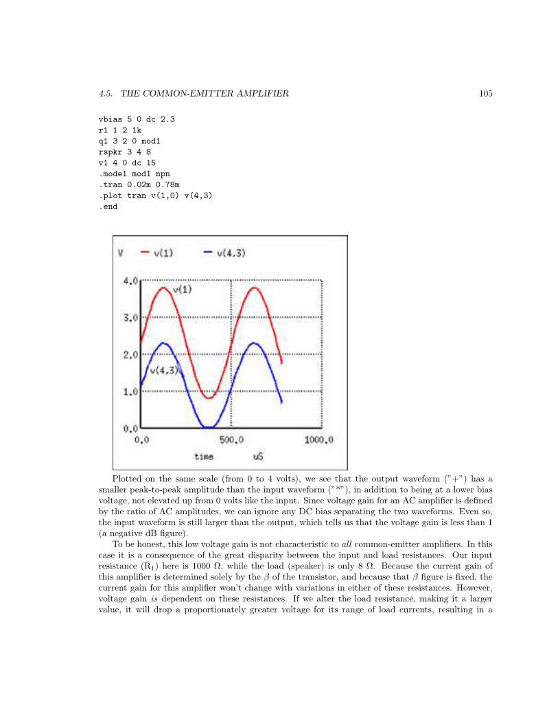
4.5. THE COMMON-EMITTER AMPLIFIER 105
vbias 5 0 dc 2.3
r1 1 2 1k
q1 3 2 0 mod1
rspkr 3 4 8
v1 4 0 dc 15
.model mod1 npn
.tran 0.02m 0.78m
.plot tran v(1,0) v(4,3)
.end
Plotted on the same scale (from 0 to 4 volts), we see that the output waveform (”+”) has asmaller peak-to-peak amplitude than the input waveform (”*”), in addition to being at a lower biasvoltage, not elevated up from 0 volts like the input. Since voltage gain for an AC amplifier is definedby the ratio of AC amplitudes, we can ignore any DC bias separating the two waveforms. Even so,the input waveform is still larger than the output, which tells us that the voltage gain is less than 1(a negative dB figure).To be honest, this low voltage gain is not characteristic to all common-emitter amplifiers. In this
case it is a consequence of the great disparity between the input and load resistances. Our inputresistance (R1) here is 1000 Ω, while the load (speaker) is only 8 Ω. Because the current gain ofthis amplifier is determined solely by the β of the transistor, and because that β figure is fixed, thecurrent gain for this amplifier won’t change with variations in either of these resistances. However,voltage gain is dependent on these resistances. If we alter the load resistance, making it a largervalue, it will drop a proportionately greater voltage for its range of load currents, resulting in a

106 CHAPTER 4. BIPOLAR JUNCTION TRANSISTORS
larger output waveform. Let’s try another simulation, only this time with a 30 Ω load instead of an8 Ω load:
common-emitter amplifier
vinput 1 5 sin (0 1.5 2000 0 0)
vbias 5 0 dc 2.3
r1 1 2 1k
q1 3 2 0 mod1
rspkr 3 4 30
v1 4 0 dc 15
.model mod1 npn
.tran 0.02m 0.78m
.plot tran v(1,0) v(4,3)
.end
This time the output voltage waveform is significantly greater in amplitude than the inputwaveform. Looking closely, we can see that the output waveform (”+”) crests between 0 and about9 volts: approximately 3 times the amplitude of the input voltage.We can perform another computer analysis of this circuit, only this time instructing SPICE to
analyze it from an AC point of view, giving us peak voltage figures for input and output instead ofa time-based plot of the waveforms:

4.5. THE COMMON-EMITTER AMPLIFIER 107
common-emitter amplifier
vinput 1 5 ac 1.5
vbias 5 0 dc 2.3
r1 1 2 1k
q1 3 2 0 mod1
rspkr 3 4 30
v1 4 0 dc 15
.model mod1 npn
.ac lin 1 2000 2000
.print ac v(1,0) v(4,3)
.end
freq v(1) v(4,3)
2.000E+03 1.500E+00 4.418E+00
Peak voltage measurements of input and output show an input of 1.5 volts and an output of4.418 volts. This gives us a voltage gain ratio of 2.9453 (4.418 V / 1.5 V), or 9.3827 dB.
AV = Vout
Vin
AV = 4.418 V1.5 V
AV = 2.9453
AV(dB) = 20 log AV(ratio)
AV(dB) = 9.3827 dB
AV(dB) = 20 log 2.9453
Because the current gain of the common-emitter amplifier is fixed by β, and since the inputand output voltages will be equal to the input and output currents multiplied by their respectiveresistors, we can derive an equation for approximate voltage gain:

108 CHAPTER 4. BIPOLAR JUNCTION TRANSISTORS
AV = β Rout
Rin
AV = (100) 30 Ω1000 Ω
AV = 3
AV(dB) = 20 log AV(ratio)
AV(dB) = 20 log 3
AV(dB) = 9.5424 dB
As you can see, the predicted results for voltage gain are quite close to the simulated results.With perfectly linear transistor behavior, the two sets of figures would exactly match. SPICE doesa reasonable job of accounting for the many ”quirks” of bipolar transistor function in its analysis,hence the slight mismatch in voltage gain based on SPICE’s output.
These voltage gains remain the same regardless of where we measure output voltage in thecircuit: across collector and emitter, or across the series load resistor as we did in the last analysis.The amount of output voltage change for any given amount of input voltage will remain the same.Consider the two following SPICE analyses as proof of this. The first simulation is time-based, toprovide a plot of input and output voltages. You will notice that the two signals are 180o out ofphase with each other. The second simulation is an AC analysis, to provide simple, peak voltagereadings for input and output:
common-emitter amplifier
vinput 1 5 sin (0 1.5 2000 0 0)
vbias 5 0 dc 2.3
r1 1 2 1k
q1 3 2 0 mod1
rspkr 3 4 30
v1 4 0 dc 15
.model mod1 npn
.tran 0.02m 0.74m
.plot tran v(1,0) v(3,0)
.end

4.5. THE COMMON-EMITTER AMPLIFIER 109
common-emitter amplifier
vinput 1 5 ac 1.5
vbias 5 0 dc 2.3
r1 1 2 1k
q1 3 2 0 mod1
rspkr 3 4 30
v1 4 0 dc 15
.model mod1 npn
.ac lin 1 2000 2000
.print ac v(1,0) v(3,0)
.end
freq v(1) v(3)
2.000E+03 1.500E+00 4.418E+00
We still have a peak output voltage of 4.418 volts with a peak input voltage of 1.5 volts. Theonly difference from the last set of simulations is the phase of the output voltage.
So far, the example circuits shown in this section have all used NPN transistors. PNP transistorsare just as valid to use as NPN in any amplifier configuration, so long as the proper polarity andcurrent directions are maintained, and the common-emitter amplifier is no exception. The invertingbehavior and gain properties of a PNP transistor amplifier are the same as its NPN counterpart,just the polarities are different:

110 CHAPTER 4. BIPOLAR JUNCTION TRANSISTORS
Vinput
Vbias
+-
• REVIEW:
• Common-emitter transistor amplifiers are so-called because the input and output voltagepoints share the emitter lead of the transistor in common with each other, not consideringany power supplies.
• Transistors are essentially DC devices: they cannot directly handle voltages or currents thatreverse direction. In order to make them work for amplifying AC signals, the input signal mustbe offset with a DC voltage to keep the transistor in its active mode throughout the entirecycle of the wave. This is called biasing.
• If the output voltage is measured between emitter and collector on a common-emitter amplifier,it will be 180o out of phase with the input voltage waveform. For this reason, the common-emitter amplifier is called an inverting amplifier circuit.
• The current gain of a common-emitter transistor amplifier with the load connected in serieswith the collector is equal to β. The voltage gain of a common-emitter transistor amplifier isapproximately given here:
•AV = β Rout
Rin
• Where ”Rout” is the resistor connected in series with the collector and ”Rin” is the resistorconnected in series with the base.
4.6 The common-collector amplifier
Our next transistor configuration to study is a bit simpler in terms of gain calculations. Called thecommon-collector configuration, its schematic diagram looks like this:

4.6. THE COMMON-COLLECTOR AMPLIFIER 111
Rload
VinVout
It is called the common-collector configuration because (ignoring the power supply battery) boththe signal source and the load share the collector lead as a common connection point:
Rload
VinVout
BC
E
It should be apparent that the load resistor in the common-collector amplifier circuit receivesboth the base and collector currents, being placed in series with the emitter. Since the emitterlead of a transistor is the one handling the most current (the sum of base and collector currents,since base and collector currents always mesh together to form the emitter current), it would bereasonable to presume that this amplifier will have a very large current gain (maximum outputcurrent for minimum input current). This presumption is indeed correct: the current gain for acommon-collector amplifier is quite large, larger than any other transistor amplifier configuration.However, this is not necessarily what sets it apart from other amplifier designs.
Let’s proceed immediately to a SPICE analysis of this amplifier circuit, and you will be able toimmediately see what is unique about this amplifier:
RloadVin
V1 15 V
Q1
5 kΩ
1
0 0 0
1
2
3
2

112 CHAPTER 4. BIPOLAR JUNCTION TRANSISTORS
common-collector amplifier
vin 1 0
q1 2 1 3 mod1
v1 2 0 dc 15
rload 3 0 5k
.model mod1 npn
.dc vin 0 5 0.2
.plot dc v(3,0)
.end
type npn
is 1.00E-16
bf 100.000
nf 1.000
br 1.000
nr 1.000
Unlike the common-emitter amplifier from the previous section, the common-collector producesan output voltage in direct rather than inverse proportion to the rising input voltage. As the inputvoltage increases, so does the output voltage. More than that, a close examination reveals that theoutput voltage is nearly identical to the input voltage, lagging behind only about 0.77 volts.

4.6. THE COMMON-COLLECTOR AMPLIFIER 113
This is the unique quality of the common-collector amplifier: an output voltage that is nearlyequal to the input voltage. Examined from the perspective of output voltage change for a givenamount of input voltage change, this amplifier has a voltage gain of almost exactly unity (1), or 0dB. This holds true for transistors of any β value, and for load resistors of any resistance value.
It is simple to understand why the output voltage of a common-collector amplifier is alwaysnearly equal to the input voltage. Referring back to the diode-regulating diode transistor model,we see that the base current must go through the base-emitter PN junction, which is equivalentto a normal rectifying diode. So long as this junction is forward-biased (the transistor conductingcurrent in either its active or saturated modes), it will have a voltage drop of approximately 0.7 volts,assuming silicon construction. This 0.7 volt drop is largely irrespective of the actual magnitude ofbase current, so we can regard it as being constant:
C
E
B
Rload
Vin
0.7 V+
-+
-
Given the voltage polarities across the base-emitter PN junction and the load resistor, we seethat they must add together to equal the input voltage, in accordance with Kirchhoff’s Voltage Law.In other words, the load voltage will always be about 0.7 volts less than the input voltage for allconditions where the transistor is conducting. Cutoff occurs at input voltages below 0.7 volts, andsaturation at input voltages in excess of battery (supply) voltage plus 0.7 volts.
Because of this behavior, the common-collector amplifier circuit is also known as the voltage-follower or emitter-follower amplifier, in reference to the fact that the input and load voltages followeach other so closely.
Applying the common-collector circuit to the amplification of AC signals requires the same input”biasing” used in the common-emitter circuit: a DC voltage must be added to the AC input signalto keep the transistor in its active mode during the entire cycle. When this is done, the result is anon-inverting amplifier:

114 CHAPTER 4. BIPOLAR JUNCTION TRANSISTORS
RloadVin
V1 15 V
Q1
5 kΩ
1
0 0
1
2
3
2
1.5 V2 kHz
4Vbias
+ -
2.3 V
common-collector amplifier
vin 1 4 sin(0 1.5 2000 0 0)
vbias 4 0 dc 2.3
q1 2 1 3 mod1
v1 2 0 dc 15
rload 3 0 5k
.model mod1 npn
.tran .02m .78m
.plot tran v(1,0) v(3,0)
.end

4.6. THE COMMON-COLLECTOR AMPLIFIER 115
Here’s another view of the circuit, this time with oscilloscopes connected to several points ofinterest:
RloadVin
V1 15 V
5 kΩ
1.5 V2 kHz
+ -
Since this amplifier configuration doesn’t provide any voltage gain (in fact, in practice it actuallyhas a voltage gain of slightly less than 1), its only amplifying factor is current. The common-emitteramplifier configuration examined in the previous section had a current gain equal to the β of thetransistor, being that the input current went through the base and the output (load) current wentthrough the collector, and β by definition is the ratio between the collector and base currents. In

116 CHAPTER 4. BIPOLAR JUNCTION TRANSISTORS
the common-collector configuration, though, the load is situated in series with the emitter, and thusits current is equal to the emitter current. With the emitter carrying collector current and basecurrent, the load in this type of amplifier has all the current of the collector running through it plusthe input current of the base. This yields a current gain of β plus 1:
AI = Iemitter
Ibase
AI = Ibase
Icollector+ Ibase
AI = Icollector
Ibase+ 1
AI = β + 1
Once again, PNP transistors are just as valid to use in the common-collector configuration asNPN transistors. The gain calculations are all the same, as is the non-inverting behavior of theamplifier. The only difference is in voltage polarities and current directions:
RloadVin
+-
A popular application of the common-collector amplifier is for regulated DC power supplies,where an unregulated (varying) source of DC voltage is clipped at a specified level to supply regulated(steady) voltage to a load. Of course, zener diodes already provide this function of voltage regulation:
RloadUnregulatedDC voltage
source
R
Regulated voltageacross load
Zenerdiode

4.6. THE COMMON-COLLECTOR AMPLIFIER 117
However, when used in this direct fashion, the amount of current that may be supplied to theload is usually quite limited. In essence, this circuit regulates voltage across the load by keepingcurrent through the series resistor at a high enough level to drop all the excess power source voltageacross it, the zener diode drawing more or less current as necessary to keep the voltage across itselfsteady. For high-current loads, an plain zener diode voltage regulator would have to be capable ofshunting a lot of current through the diode in order to be effective at regulating load voltage in theevent of large load resistance or voltage source changes.
One popular way to increase the current-handling ability of a regulator circuit like this is to usea common-collector transistor to amplify current to the load, so that the zener diode circuit onlyhas to handle the amount of current necessary to drive the base of the transistor:
RloadUnregulatedDC voltage
source
R
Zenerdiode
There’s really only one caveat to this approach: the load voltage will be approximately 0.7 voltsless than the zener diode voltage, due to the transistor’s 0.7 volt base-emitter drop. However, sincethis 0.7 volt difference is fairly constant over a wide range of load currents, a zener diode with a 0.7volt higher rating can be chosen for the application.
Sometimes the high current gain of a single-transistor, common-collector configuration isn’tenough for a particular application. If this is the case, multiple transistors may be staged togetherin a popular configuration known as a Darlington pair, just an extension of the common-collectorconcept:
B
C
E
An NPN "Darlington pair"

118 CHAPTER 4. BIPOLAR JUNCTION TRANSISTORS
Darlington pairs essentially place one transistor as the common-collector load for another transis-tor, thus multiplying their individual current gains. Base current through the upper-left transistor isamplified through that transistor’s emitter, which is directly connected to the base of the lower-righttransistor, where the current is again amplified. The overall current gain is as follows:
AI = (β1 + 1)(β2 + 1)
Darlington pair current gain
Where,β1 = Beta of first transistorβ2 = Beta of second transistor
Voltage gain is still nearly equal to 1 if the entire assembly is connected to a load in common-collector fashion, although the load voltage will be a full 1.4 volts less than the input voltage:
Rload
VinVout
Vout = Vin - 1.4
+
-
+-0.7 V
+-0.7 V
Darlington pairs may be purchased as discrete units (two transistors in the same package), or maybe built up from a pair of individual transistors. Of course, if even more current gain is desired thanwhat may be obtained with a pair, Darlington triplet or quadruplet assemblies may be constructed.
• REVIEW:
• Common-collector transistor amplifiers are so-called because the input and output voltagepoints share the collector lead of the transistor in common with each other, not consideringany power supplies.
• The output voltage on a common-collector amplifier will be in phase with the input voltage,making the common-collector a non-inverting amplifier circuit.
• The current gain of a common-collector amplifier is equal to β plus 1. The voltage gain isapproximately equal to 1 (in practice, just a little bit less).
• A Darlington pair is a pair of transistors ”piggybacked” on one another so that the emitter ofone feeds current to the base of the other in common-collector form. The result is an overall

4.7. THE COMMON-BASE AMPLIFIER 119
current gain equal to the product (multiplication) of their individual common-collector currentgains (β plus 1).
4.7 The common-base amplifier
The final transistor amplifier configuration we need to study is the common-base. This configurationis more complex than the other two, and is less common due to its strange operating characteristics.
Vin
Rload
It is called the common-base configuration because (DC power source aside), the signal sourceand the load share the base of the transistor as a common connection point:
Vin
Rload
BC
E
Vout
Perhaps the most striking characteristic of this configuration is that the input signal sourcemust carry the full emitter current of the transistor, as indicated by the heavy arrows in the firstillustration. As we know, the emitter current is greater than any other current in the transistor,being the sum of base and collector currents. In the last two amplifier configurations, the signalsource was connected to the base lead of the transistor, thus handling the least current possible.Because the input current exceeds all other currents in the circuit, including the output current,
the current gain of this amplifier is actually less than 1 (notice how Rload is connected to the collector,thus carrying slightly less current than the signal source). In other words, it attenuates current

120 CHAPTER 4. BIPOLAR JUNCTION TRANSISTORS
rather than amplifying it. With common-emitter and common-collector amplifier configurations,the transistor parameter most closely associated with gain was β. In the common-base circuit, wefollow another basic transistor parameter: the ratio between collector current and emitter current,which is a fraction always less than 1. This fractional value for any transistor is called the alpharatio, or α ratio.
Since it obviously can’t boost signal current, it only seems reasonable to expect it to boost signalvoltage. A SPICE simulation will vindicate that assumption:
Vin
Rload
V1 15 V
Q1
5 kΩ
R1
100 Ω
0
1 2
3 4
common-base amplifier
vin 0 1
r1 1 2 100
q1 4 0 2 mod1
v1 3 0 dc 15
rload 3 4 5k
.model mod1 npn
.dc vin 0.6 1.2 .02
.plot dc v(3,4)
.end

4.7. THE COMMON-BASE AMPLIFIER 121
Notice how in this simulation the output voltage goes from practically nothing (cutoff) to 15.75volts (saturation) with the input voltage being swept over a range of 0.6 volts to 1.2 volts. In fact,the output voltage plot doesn’t show a rise until about 0.7 volts at the input, and cuts off (flattens)at about 1.12 volts input. This represents a rather large voltage gain with an output voltage spanof 15.75 volts and an input voltage span of only 0.42 volts: a gain ratio of 37.5, or 31.48 dB. Noticealso how the output voltage (measured across Rload) actually exceeds the power supply (15 volts)at saturation, due to the series-aiding effect of the the input voltage source.
A second set of SPICE analyses with an AC signal source (and DC bias voltage) tells the samestory: a high voltage gain.

122 CHAPTER 4. BIPOLAR JUNCTION TRANSISTORS
Vin
Rload
V1 15 V
Q1
5 kΩ
R1
100 Ω
0
1
2
3 4
Vbias
5
0.12 V2 kHz
0.95 V
Vout
common-base amplifier
vin 0 1 sin (0 0.12 2000 0 0)
vbias 1 5 dc 0.95
r1 5 2 100
q1 4 0 2 mod1
v1 3 0 dc 15
rload 3 4 5k
.model mod1 npn
.tran 0.02m 0.78m
.plot tran v(1,0) v(4,3)
.end

4.7. THE COMMON-BASE AMPLIFIER 123
As you can see, the input and output waveforms are in phase with each other. This tells us thatthe common-base amplifier is non-inverting.
common-base amplifier
vin 0 1 ac 0.12
vbias 1 5 dc 0.95
r1 5 2 100
q1 4 0 2 mod1
v1 3 0 dc 15
rload 3 4 5k
.model mod1 npn
.ac lin 1 2000 2000
.print ac v(1,0) v(3,4)
.end
freq v(1) v(3,4)
2.000E+03 1.200E-01 5.129E+00
Voltage figures from the second analysis (AC mode) show a voltage gain of 42.742 (5.129 V /0.12 V), or 32.617 dB:

124 CHAPTER 4. BIPOLAR JUNCTION TRANSISTORS
AV = Vout
Vin
AV =
AV =
AV(dB) = 20 log AV(ratio)
5.129 V0.12 V
42.742
AV(dB) = 20 log 42.742
AV(dB) = 32.617 dB
Here’s another view of the circuit, showing the phase relations and DC offsets of various signalsin the circuit just simulated:
Vin
Vbias
Rload
. . . and for a PNP transistor:

4.7. THE COMMON-BASE AMPLIFIER 125
Vin
Vbias
Rload
Predicting voltage gain for the common-base amplifier configuration is quite difficult, and in-volves approximations of transistor behavior that are difficult to measure directly. Unlike the otheramplifier configurations, where voltage gain was either set by the ratio of two resistors (common-emitter), or fixed at an unchangeable value (common-collector), the voltage gain of the common-baseamplifier depends largely on the amount of DC bias on the input signal. As it turns out, the internaltransistor resistance between emitter and base plays a major role in determining voltage gain, andthis resistance changes with different levels of current through the emitter.While this phenomenon is difficult to explain, it is rather easy to demonstrate through the use of
computer simulation. What I’m going to do here is run several SPICE simulations on a common-baseamplifier circuit, changing the DC bias voltage slightly while keeping the AC signal amplitude andall other circuit parameters constant. As the voltage gain changes from one simulation to another,different output voltage amplitudes will be noticed as a result.Although these analyses will all be conducted in the AC mode, they were first ”proofed” in
the transient analysis mode (voltage plotted over time) to ensure that the entire wave was beingfaithfully reproduced and not ”clipped” due to improper biasing. No meaningful calculations of gaincan be based on waveforms that are distorted:
common-base amplifier DC bias = 0.85 volts
vin 0 1 ac 0.08
vbias 1 5 dc 0.85
r1 5 2 100
q1 4 0 2 mod1
v1 3 0 dc 15
rload 3 4 5k
.model mod1 npn
.ac lin 1 2000 2000

126 CHAPTER 4. BIPOLAR JUNCTION TRANSISTORS
.print ac v(1,0) v(3,4)
.end
freq v(1) v(3,4)
2.000E+03 8.000E-02 3.005E+00
common-base amplifier dc bias = 0.9 volts
vin 0 1 ac 0.08
vbias 1 5 dc 0.90
r1 5 2 100
q1 4 0 2 mod1
v1 3 0 dc 15
rload 3 4 5k
.model mod1 npn
.ac lin 1 2000 2000
.print ac v(1,0) v(3,4)
.end
freq v(1) v(3,4)
2.000E+03 8.000E-02 3.264E+00
common-base amplifier dc bias = 0.95 volts
vin 0 1 ac 0.08
vbias 1 5 dc 0.95
r1 5 2 100
q1 4 0 2 mod1
v1 3 0 dc 15
rload 3 4 5k
.model mod1 npn
.ac lin 1 2000 2000
.print ac v(1,0) v(3,4)
.end
freq v(1) v(3,4)
2.000E+03 8.000E-02 3.419E+00
A trend should be evident here: with increases in DC bias voltage, voltage gain increases as well.We can see that the voltage gain is increasing because each subsequent simulation produces greateroutput voltage for the exact same input signal voltage (0.08 volts). As you can see, the changes arequite large, and they are caused by miniscule variations in bias voltage!The combination of very low current gain (always less than 1) and somewhat unpredictable
voltage gain conspire against the common-base design, relegating it to few practical applications.
• REVIEW:

4.8. BIASING TECHNIQUES 127
• Common-base transistor amplifiers are so-called because the input and output voltage pointsshare the base lead of the transistor in common with each other, not considering any powersupplies.
• The current gain of a common-base amplifier is always less than 1. The voltage gain is afunction of input and output resistances, and also the internal resistance of the emitter-basejunction, which is subject to change with variations in DC bias voltage. Suffice to say that thevoltage gain of a common-base amplifier can be very high.
• The ratio of a transistor’s collector current to emitter current is called α. The α value for anytransistor is always less than unity, or in other words, less than 1.
4.8 Biasing techniques
In the common-emitter section of this chapter, we saw a SPICE analysis where the output waveformresembled a half-wave rectified shape: only half of the input waveform was reproduced, with theother half being completely cut off. Since our purpose at that time was to reproduce the entirewaveshape, this constituted a problem. The solution to this problem was to add a small bias voltageto the amplifier input so that the transistor stayed in active mode throughout the entire wave cycle.This addition was called a bias voltage.
There are applications, though, where a half-wave output is not problematic. In fact, someapplications may necessitate this very type of amplification. Because it is possible to operate anamplifier in modes other than full-wave reproduction, and because there are specific applicationsrequiring different ranges of reproduction, it is useful to describe the degree to which an amplifierreproduces the input waveform by designating it according to class. Amplifier class operation iscategorized by means of alphabetical letters: A, B, C, and AB.
Class A operation is where the entire input waveform is faithfully reproduced. Although I didn’tintroduce this concept back in the common-emitter section, this is what we were hoping to attain inour simulations. Class A operation can only be obtained when the transistor spends its entire timein the active mode, never reaching either cutoff or saturation. To achieve this, sufficient DC biasvoltage is usually set at the level necessary to drive the transistor exactly halfway between cutoffand saturation. This way, the AC input signal will be perfectly ”centered” between the amplifier’shigh and low signal limit levels.

128 CHAPTER 4. BIPOLAR JUNCTION TRANSISTORS
Vinput
Vbias
Amplifier
Class A operation
Class B operation is what we had the first time an AC signal was applied to the common-emitteramplifier with no DC bias voltage. The transistor spent half its time in active mode and the otherhalf in cutoff with the input voltage too low (or even of the wrong polarity!) to forward-bias itsbase-emitter junction.
Vinput
Amplifier
Class B operation
Little or noDC bias voltage
By itself, an amplifier operating in class B mode is not very useful. In most circumstances, thesevere distortion introduced into the waveshape by eliminating half of it would be unacceptable.However, class B operation is a useful mode of biasing if two amplifiers are operated as a push-pullpair, each amplifier handling only half of the waveform at a time:

4.8. BIASING TECHNIQUES 129
Voutput
Input componentsomitted for simplicity
Powersupply
Q1
Q2
Transistor Q1 ”pushes” (drives the output voltage in a positive direction with respect to ground),while transistor Q2 ”pulls” the output voltage (in a negative direction, toward 0 volts with respectto ground). Individually, each of these transistors is operating in class B mode, active only forone-half of the input waveform cycle. Together, however, they function as a team to produce anoutput waveform identical in shape to the input waveform.
A decided advantage of the class B (push-pull) amplifier design over the class A design is greateroutput power capability. With a class A design, the transistor dissipates a lot of energy in the formof heat because it never stops conducting current. At all points in the wave cycle it is in the active(conducting) mode, conducting substantial current and dropping substantial voltage. This meansthere is substantial power dissipated by the transistor throughout the cycle. In a class B design, eachtransistor spends half the time in cutoff mode, where it dissipates zero power (zero current = zeropower dissipation). This gives each transistor a time to ”rest” and cool while the other transistorcarries the burden of the load. Class A amplifiers are simpler in design, but tend to be limited tolow-power signal applications for the simple reason of transistor heat dissipation.
There is another class of amplifier operation known as class AB, which is somewhere betweenclass A and class B: the transistor spends more than 50% but less than 100% of the time conductingcurrent.
If the input signal bias for an amplifier is slightly negative (opposite of the bias polarity forclass A operation), the output waveform will be further ”clipped” than it was with class B biasing,resulting in an operation where the transistor spends the majority of the time in cutoff mode:

130 CHAPTER 4. BIPOLAR JUNCTION TRANSISTORS
Vinput
Amplifier
Class C operation
Vbias
At first, this scheme may seem utterly pointless. After all, how useful could an amplifier be if itclips the waveform as badly as this? If the output is used directly with no conditioning of any kind,it would indeed be of questionable utility. However, with the application of a tank circuit (parallelresonant inductor-capacitor combination) to the output, the occasional output surge produced bythe amplifier can set in motion a higher-frequency oscillation maintained by the tank circuit. Thismay be likened to a machine where a heavy flywheel is given an occasional ”kick” to keep it spinning:
Vinput
Amplifier
Class C operation
Vbias
with resonant output
Called class C operation, this scheme also enjoys high power efficiency due to the fact thatthe transistor(s) spend the vast majority of time in the cutoff mode, where they dissipate zeropower. The rate of output waveform decay (decreasing oscillation amplitude between ”kicks” fromthe amplifier) is exaggerated here for the benefit of illustration. Because of the tuned tank circuiton the output, this type of circuit is usable only for amplifying signals of definite, fixed frequency.Another type of amplifier operation, significantly different from Class A, B, AB, or C, is called
Class D. It is not obtained by applying a specific measure of bias voltage as are the other classes ofoperation, but requires a radical re-design of the amplifier circuit itself. It’s a little too early in this

4.8. BIASING TECHNIQUES 131
chapter to investigate exactly how a class D amplifier is built, but not too early to discuss its basicprinciple of operation.A class D amplifier reproduces the profile of the input voltage waveform by generating a rapidly-
pulsing squarewave output. The duty cycle of this output waveform (time ”on” versus total cycletime) varies with the instantaneous amplitude of the input signal. The following plots demonstratethis principle:
Input
Output
Class D operation
The greater the instantaneous voltage of the input signal, the greater the duty cycle of the outputsquarewave pulse. If there can be any goal stated of the class D design, it is to avoid active-modetransistor operation. Since the output transistor of a class D amplifier is never in the active mode,only cutoff or saturated, there will be little heat energy dissipated by it. This results in very highpower efficiency for the amplifier. Of course, the disadvantage of this strategy is the overwhelmingpresence of harmonics on the output. Fortunately, since these harmonic frequencies are typicallymuch greater than the frequency of the input signal, they can be filtered out by a low-pass filterwith relative ease, resulting in an output more closely resembling the original input signal waveform.Class D technology is typically seen where extremely high power levels and relatively low frequenciesare encountered, such as in industrial inverters (devices converting DC into AC power to run motorsand other large devices) and high-performance audio amplifiers.A term you will likely come across in your studies of electronics is something called quiescent,
which is a modifier designating the normal, or zero input signal, condition of a circuit. Quiescentcurrent, for example, is the amount of current in a circuit with zero input signal voltage applied. Biasvoltage in a transistor circuit forces the transistor to operate at a different level of collector currentwith zero input signal voltage than it would without that bias voltage. Therefore, the amount ofbias in an amplifier circuit determines its quiescent values.In a class A amplifier, the quiescent current should be exactly half of its saturation value (halfway
between saturation and cutoff, cutoff by definition being zero). Class B and class C amplifiers havequiescent current values of zero, since they are supposed to be cutoff with no signal applied. ClassAB amplifiers have very low quiescent current values, just above cutoff. To illustrate this graphically,
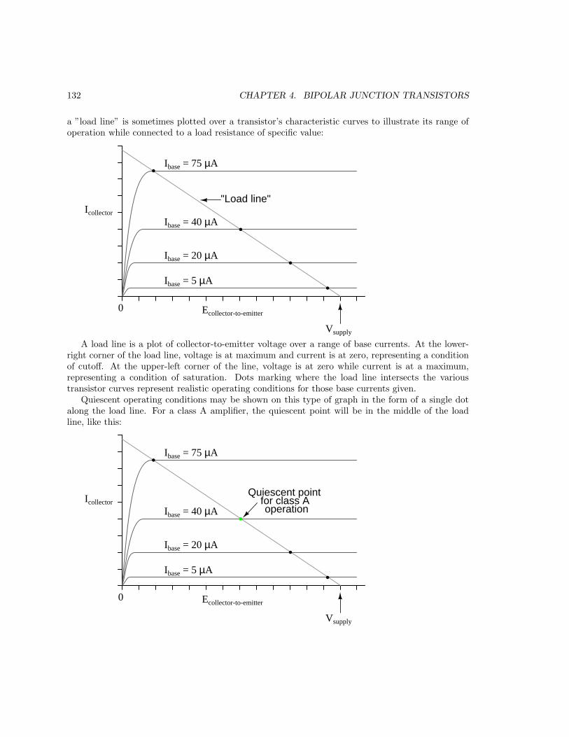
132 CHAPTER 4. BIPOLAR JUNCTION TRANSISTORS
a ”load line” is sometimes plotted over a transistor’s characteristic curves to illustrate its range ofoperation while connected to a load resistance of specific value:
Icollector
Ecollector-to-emitter
"Load line"
Vsupply
0
Ibase = 75 µA
Ibase = 40 µA
Ibase = 20 µA
Ibase = 5 µA
A load line is a plot of collector-to-emitter voltage over a range of base currents. At the lower-right corner of the load line, voltage is at maximum and current is at zero, representing a conditionof cutoff. At the upper-left corner of the line, voltage is at zero while current is at a maximum,representing a condition of saturation. Dots marking where the load line intersects the varioustransistor curves represent realistic operating conditions for those base currents given.Quiescent operating conditions may be shown on this type of graph in the form of a single dot
along the load line. For a class A amplifier, the quiescent point will be in the middle of the loadline, like this:
Icollector
Ecollector-to-emitter
Vsupply
0
Quiescent pointfor class A operation
Ibase = 75 µA
Ibase = 40 µA
Ibase = 20 µA
Ibase = 5 µA
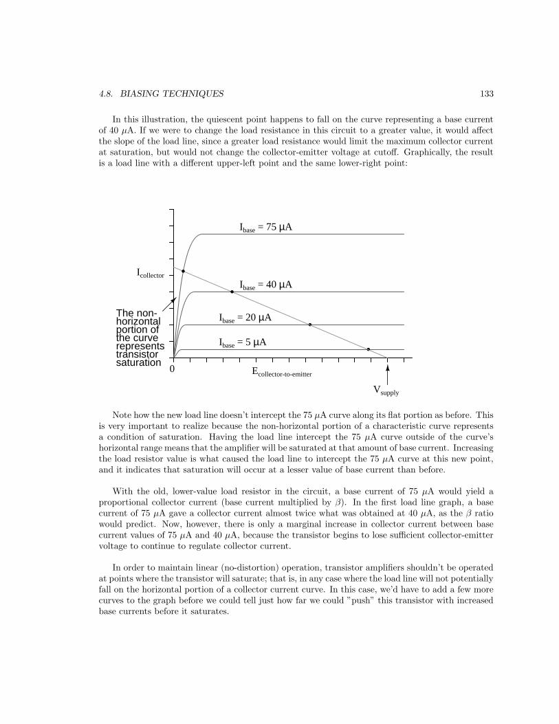
4.8. BIASING TECHNIQUES 133
In this illustration, the quiescent point happens to fall on the curve representing a base currentof 40 µA. If we were to change the load resistance in this circuit to a greater value, it would affectthe slope of the load line, since a greater load resistance would limit the maximum collector currentat saturation, but would not change the collector-emitter voltage at cutoff. Graphically, the resultis a load line with a different upper-left point and the same lower-right point:
Icollector
Ecollector-to-emitter
Vsupply
0
Ibase = 75 µA
Ibase = 40 µA
Ibase = 20 µA
Ibase = 5 µA
The non-horizontalportion ofthe curverepresentstransistorsaturation
Note how the new load line doesn’t intercept the 75 µA curve along its flat portion as before. Thisis very important to realize because the non-horizontal portion of a characteristic curve representsa condition of saturation. Having the load line intercept the 75 µA curve outside of the curve’shorizontal range means that the amplifier will be saturated at that amount of base current. Increasingthe load resistor value is what caused the load line to intercept the 75 µA curve at this new point,and it indicates that saturation will occur at a lesser value of base current than before.
With the old, lower-value load resistor in the circuit, a base current of 75 µA would yield aproportional collector current (base current multiplied by β). In the first load line graph, a basecurrent of 75 µA gave a collector current almost twice what was obtained at 40 µA, as the β ratiowould predict. Now, however, there is only a marginal increase in collector current between basecurrent values of 75 µA and 40 µA, because the transistor begins to lose sufficient collector-emittervoltage to continue to regulate collector current.
In order to maintain linear (no-distortion) operation, transistor amplifiers shouldn’t be operatedat points where the transistor will saturate; that is, in any case where the load line will not potentiallyfall on the horizontal portion of a collector current curve. In this case, we’d have to add a few morecurves to the graph before we could tell just how far we could ”push” this transistor with increasedbase currents before it saturates.

134 CHAPTER 4. BIPOLAR JUNCTION TRANSISTORS
Icollector
Ecollector-to-emitter
Vsupply
0
Ibase = 50 µA
Ibase = 40 µA
Ibase = 75 µA
Ibase = 20 µA
Ibase = 5 µA
Ibase = 60 µA
It appears in this graph that the highest-current point on the load line falling on the straightportion of a curve is the point on the 50 µA curve. This new point should be considered the maximumallowable input signal level for class A operation. Also for class A operation, the bias should be setso that the quiescent point is halfway between this new maximum point and cutoff:
Icollector
Ecollector-to-emitter
Vsupply
0
Ibase = 50 µA
Ibase = 40 µA
Ibase = 75 µA
Ibase = 20 µA
Ibase = 5 µA
Ibase = 60 µA
New quiescent point
Now that we know a little more about the consequences of different DC bias voltage levels, itis time to investigate practical biasing techniques. So far, I’ve shown a small DC voltage source(battery) connected in series with the AC input signal to bias the amplifier for whatever desiredclass of operation. In real life, the connection of a precisely-calibrated battery to the input of anamplifier is simply not practical. Even if it were possible to customize a battery to produce justthe right amount of voltage for any given bias requirement, that battery would not remain at its

4.8. BIASING TECHNIQUES 135
manufactured voltage indefinitely. Once it started to discharge and its output voltage drooped, theamplifier would begin to drift in the direction of class B operation.
Take this circuit, illustrated in the common-emitter section for a SPICE simulation, for instance:
speaker
V1 15 VQ1
R1
1 kΩ
8 Ω
1
0 0
2
3 4
Vinput
1.5 V2 kHz
Vbias
5
2.3 V
+ -
That 2.3 volt ”Vbias” battery would not be practical to include in a real amplifier circuit. A farmore practical method of obtaining bias voltage for this amplifier would be to develop the necessary2.3 volts using a voltage divider network connected across the 15 volt battery. After all, the 15 voltbattery is already there by necessity, and voltage divider circuits are very easy to design and build.Let’s see how this might look:
speaker
V1 15 VQ1
R1
1 kΩ
8 Ω
1
0 0
2
3 4
Vinput
1.5 V2 kHz
Vbias
4
0
R2
R3
0
If we choose a pair of resistor values for R2 and R3 that will produce 2.3 volts across R3 from atotal of 15 volts (such as 8466 Ω for R2 and 1533 Ω for R3), we should have our desired value of 2.3volts between base and emitter for biasing with no signal input. The only problem is, this circuitconfiguration places the AC input signal source directly in parallel with R3 of our voltage divider.This is not acceptable, as the AC source will tend to overpower any DC voltage dropped across R3.Parallel components must have the same voltage, so if an AC voltage source is directly connectedacross one resistor of a DC voltage divider, the AC source will ”win” and there will be no DC biasvoltage added to the signal.
One way to make this scheme work, although it may not be obvious why it will work, is to placea coupling capacitor between the AC voltage source and the voltage divider like this:

136 CHAPTER 4. BIPOLAR JUNCTION TRANSISTORS
speaker
V1 15 VQ1
R1
1 kΩ
8 Ω
1
0 0
2
3 4
Vinput
1.5 V2 kHz
4
0
R2
R3
0
5C
5
8.466 kΩ
1.533 kΩ
The capacitor forms a high-pass filter between the AC source and the DC voltage divider, passingalmost all of the AC signal voltage on to the transistor while blocking all DC voltage from beingshorted through the AC signal source. This makes much more sense if you understand the super-position theorem and how it works. According to superposition, any linear, bilateral circuit can beanalyzed in a piecemeal fashion by only considering one power source at a time, then algebraicallyadding the effects of all power sources to find the final result. If we were to separate the capacitorand R2−−R3 voltage divider circuit from the rest of the amplifier, it might be easier to understandhow this superposition of AC and DC would work.
With only the AC signal source in effect, and a capacitor with an arbitrarily low impedance atsignal frequency, almost all the AC voltage appears across R3:
Vinput
1.5 V2 kHz
R2
R31.533
kΩ
8.466kΩ
Due to the capacitor’s very low impedance at
≈ 1.5 V2 kHz
signal frequency, it behaves much like a straightpiece of wire and thus can be omitted for the purpose of this step in superposition analysis.
With only the DC source in effect, the capacitor appears to be an open circuit, and thus neitherit nor the shorted AC signal source will have any effect on the operation of the R2−−R3 voltagedivider:

4.8. BIASING TECHNIQUES 137
R2
R31.533
kΩ
8.466kΩ
V1 15 V
2.3 V
The capacitor appears to be an open circuitas far as DC analysis is concerned
Combining these two separate analyses, we get a superposition of (almost) 1.5 volts AC and 2.3volts DC, ready to be connected to the base of the transistor:
V1 15 VVinput
1.5 V2 kHz
R2
R3
C
1.533kΩ
8.466kΩ
Enough talk – it’s about time for a SPICE simulation of the whole amplifier circuit. I’ll use acapacitor value of 100 µF to obtain an arbitrarily low (0.796 Ω) impedance at 2000 Hz:
voltage divider biasing
vinput 1 0 sin (0 1.5 2000 0 0)
c1 1 5 100u
r1 5 2 1k
r2 4 5 8466
r3 5 0 1533
q1 3 2 0 mod1
rspkr 3 4 8
v1 4 0 dc 15
.model mod1 npn
.tran 0.02m 0.78m
.plot tran v(1,0) i(v1)
.end

138 CHAPTER 4. BIPOLAR JUNCTION TRANSISTORS
Notice that there is substantial distortion in the output waveform here: the sine wave is beingclipped during most of the input signal’s negative half-cycle. This tells us the transistor is enteringinto cutoff mode when it shouldn’t (I’m assuming a goal of class A operation as before). Why isthis? This new biasing technique should give us exactly the same amount of DC bias voltage asbefore, right?
With the capacitor and R2−−R3 resistor network unloaded, it will provide exactly 2.3 voltsworth of DC bias. However, once we connect this network to the transistor, it is no longer unloaded.Current drawn through the base of the transistor will load the voltage divider, thus reducing theDC bias voltage available for the transistor. Using the diode-regulating diode transistor model toillustrate, the bias problem becomes evident:
speaker
V1
Q1
R1
Vinput
R2
R3
C
IR3
Ibias
IR3 + Ibias
IR3
A voltage divider’s output depends not only on the size of its constituent resistors, but also on

4.8. BIASING TECHNIQUES 139
how much current is being divided away from it through a load. In this case, the base-emitter PNjunction of the transistor is a load that decreases the DC voltage dropped across R3, due to the factthat the bias current joins with R3’s current to go through R2, upsetting the divider ratio formerlyset by the resistance values of R2 and R3. In order to obtain a DC bias voltage of 2.3 volts, thevalues of R2 and/or R3 must be adjusted to compensate for the effect of base current loading. Inthis case, we want to increase the DC voltage dropped across R3, so we can lower the value of R2,raise the value of R3, or both.
voltage divider biasing
vinput 1 0 sin (0 1.5 2000 0 0)
c1 1 5 100u
r1 5 2 1k
r2 4 5 6k <--- R2 decreased to 6 k ohms
r3 5 0 4k <--- R3 increased to 4 k ohms
q1 3 2 0 mod1
rspkr 3 4 8
v1 4 0 dc 15
.model mod1 npn
.tran 0.02m 0.78m
.plot tran v(1,0) i(v1)
.end

140 CHAPTER 4. BIPOLAR JUNCTION TRANSISTORS
As you can see, the new resistor values of 6 kΩ and 4 kΩ (R2 and R3, respectively) results inclass A waveform reproduction, just the way we wanted.
• REVIEW:
• Class A operation is where an amplifier is biased so as to be in the active mode throughoutthe entire waveform cycle, thus faithfully reproducing the whole waveform.
• Class B operation is where an amplifier is biased so that only half of the input waveform getsreproduced: either the positive half or the negative half. The transistor spends half its timein the active mode and half its time cutoff. Complementary pairs of transistors running inclass B operation are often used to deliver high power amplification in audio signal systems,each transistor of the pair handling a separate half of the waveform cycle. Class B operationdelivers better power efficiency than a class A amplifier of similar output power.
• Class AB operation is where an amplifier is biased at a point somewhere between class A andclass B.
• Class C operation is where an amplifier’s bias forces it to amplify only a small portion of thewaveform. A majority of the transistor’s time is spent in cutoff mode. In order for there tobe a complete waveform at the output, a resonant tank circuit is often used as a ”flywheel”to maintain oscillations for a few cycles after each ”kick” from the amplifier. Because thetransistor is not conducting most of the time, power efficiencies are very high for a class Camplifier.
• Class D operation requires an advanced circuit design, and functions on the principle of repre-senting instantaneous input signal amplitude by the duty cycle of a high-frequency squarewave.The output transistor(s) never operate in active mode, only cutoff and saturation. Thus, thereis very little heat energy dissipated and energy efficiency is high.
• DC bias voltage on the input signal, necessary for certain classes of operation (especially classA and class C), may be obtained through the use of a voltage divider and coupling capacitorrather than a battery connected in series with the AC signal source.
4.9 Input and output coupling
To overcome the challenge of creating necessary DC bias voltage for an amplifier’s input signalwithout resorting to the insertion of a battery in series with the AC signal source, we used a voltagedivider connected across the DC power source. To make this work in conjunction with an AC inputsignal, we ”coupled” the signal source to the divider through a capacitor, which acted as a high-passfilter. With that filtering in place, the low impedance of the AC signal source couldn’t ”short out”the DC voltage dropped across the bottom resistor of the voltage divider. A simple solution, butnot without any disadvantages.Most obvious is the fact that using a high-pass filter capacitor to couple the signal source to
the amplifier means that the amplifier can only amplify AC signals. A steady, DC voltage appliedto the input would be blocked by the coupling capacitor just as much as the voltage divider biasvoltage is blocked from the input source. Furthermore, since capacitive reactance is frequency-dependent, lower-frequency AC signals will not be amplified as much as higher-frequency signals.

4.9. INPUT AND OUTPUT COUPLING 141
Non-sinusoidal signals will tend to be distorted, as the capacitor responds differently to each of thesignal’s constituent harmonics. An extreme example of this would be a low-frequency square-wavesignal:
V1
Vinput
R2
R3
C
Incidentally, this same problem occurs when oscilloscope inputs are set to the ”AC coupling”mode. In this mode, a coupling capacitor is inserted in series with the measured voltage signal toeliminate any vertical offset of the displayed waveform due to DC voltage combined with the signal.This works fine when the AC component of the measured signal is of a fairly high frequency, and thecapacitor offers little impedance to the signal. However, if the signal is of a low frequency, and/orcontains considerable levels of harmonics over a wide frequency range, the oscilloscope’s display ofthe waveform will not be accurate.
trigger
timebase
s/divDC GND AC
X
GNDDCV/div
vertical
OSCILLOSCOPE
Y
AC
Hz
FUNCTION GENERATOR
1 10 100 1k 10k 100k 1M
outputDCfinecoarse
40.00
With DC coupling, the oscilloscope properly indicates the shapeof the square wave coming from the signal generator.

142 CHAPTER 4. BIPOLAR JUNCTION TRANSISTORS
trigger
timebase
s/divDC GND AC
X
GNDDCV/div
vertical
OSCILLOSCOPE
Y
AC
Hz
FUNCTION GENERATOR
1 10 100 1k 10k 100k 1M
outputDCfinecoarse
40.00
With AC coupling, the high-pass filtering of the coupling capacitordistorts the square wave’s shape so that what is seen is notan accurate representation of the real voltage signal.
In applications where the limitations of capacitive coupling would be intolerable, another solutionmay be used: direct coupling. Direct coupling avoids the use of capacitors or any other frequency-dependent coupling component in favor of resistors. A direct-coupled amplifier circuit might looksomething like this:
speaker
V1Q11
0 0
2
3 4
Vinput
4
0
R2
R3
0
Rinput
With no capacitor to filter the input signal, this form of coupling exhibits no frequency depen-dence. DC and AC signals alike will be amplified by the transistor with the same gain (the transistoritself may tend to amplify some frequencies better than others, but that is another subject entirely!).
If direct coupling works for DC as well as for AC signals, then why use capacitive coupling forany application? One reason might be to avoid any unwanted DC bias voltage naturally presentin the signal to be amplified. Some AC signals may be superimposed on an uncontrolled DCvoltage right from the source, and an uncontrolled DC voltage would make reliable transistor biasing

4.9. INPUT AND OUTPUT COUPLING 143
impossible. The high-pass filtering offered by a coupling capacitor would work well here to avoidbiasing problems.
Another reason to use capacitive coupling rather than direct is its relative lack of signal atten-uation. Direct coupling through a resistor has the disadvantage of diminishing, or attenuating, theinput signal so that only a fraction of it reaches the base of the transistor. In many applications,some attenuation is necessary anyway to prevent normal signal levels from ”overdriving” the transis-tor into cutoff and saturation, so any attenuation inherent to the coupling network is useful anyway.However, some applications require that there be no signal loss from the input connection to thetransistor’s base for maximum voltage gain, and a direct coupling scheme with a voltage divider forbias simply won’t suffice.
So far, we’ve discussed a couple of methods for coupling an input signal to an amplifier, buthaven’t addressed the issue of coupling an amplifier’s output to a load. The example circuit used toillustrate input coupling will serve well to illustrate the issues involved with output coupling.
In our example circuit, the load is a speaker. Most speakers are electromagnetic in design: thatis, they use the force generated by an lightweight electromagnet coil suspended within a strongpermanent-magnet field to move a thin paper or plastic cone, producing vibrations in the air whichour ears interpret as sound. An applied voltage of one polarity moves the cone outward, while avoltage of the opposite polarity will move the cone inward. To exploit cone’s full freedom of motion,the speaker must receive true (unbiased) AC voltage. DC bias applied to the speaker coil tends tooffset the cone from its natural center position, and this tends to limit the amount of back-and-forthmotion it can sustain from the applied AC voltage without overtraveling. However, our examplecircuit applies a varying voltage of only one polarity across the speaker, because the speaker isconnected in series with the transistor which can only conduct current one way. This situationwould be unacceptable in the case of any high-power audio amplifier.
Somehow we need to isolate the speaker from the DC bias of the collector current so that it onlyreceives AC voltage. One way to achieve this goal is to couple the transistor collector circuit to thespeaker through a transformer:

144 CHAPTER 4. BIPOLAR JUNCTION TRANSISTORS
speaker
V1Q1
Vinput
RR
R
Voltage induced in the secondary (speaker-side) of the transformer will be strictly due to varia-tions in collector current, because the mutual inductance of a transformer only works on changes inwinding current. In other words, only the AC portion of the collector current signal will be coupledto the secondary side for powering the speaker. The speaker will ”see” true alternating current atits terminals, without any DC bias.
Transformer output coupling works, and has the added benefit of being able to provide impedancematching between the transistor circuit and the speaker coil with custom winding ratios. However,transformers tend to be large and heavy, especially for high-power applications. Also, it is difficultto engineer a transformer to handle signals over a wide range of frequencies, which is almost alwaysrequired for audio applications. To make matters worse, DC current through the primary windingadds to the magnetization of the core in one polarity only, which tends to make the transformercore saturate more easily in one AC polarity cycle than the other. This problem is reminiscent ofhaving the speaker directly connected in series with the transistor: a DC bias current tends to limithow much output signal amplitude the system can handle without distortion. Generally, though, atransformer can be designed to handle a lot more DC bias current than a speaker without runninginto trouble, so transformer coupling is still a viable solution in most cases.
Another method to isolate the speaker from DC bias in the output signal is to alter the circuita bit and use a coupling capacitor in a manner similar to coupling the input signal to the amplifier:

4.9. INPUT AND OUTPUT COUPLING 145
speaker
V1Q1
Vinput
CR
R
R
R
This circuit resembles the more conventional form of common-emitter amplifier, with the tran-sistor collector connected to the battery through a resistor. The capacitor acts as a high-pass filter,passing most of the AC voltage to the speaker while blocking all DC voltage. Again, the valueof this coupling capacitor is chosen so that its impedance at the expected signal frequency will bearbitrarily low.
The blocking of DC voltage from an amplifier’s output, be it via a transformer or a capacitor,is useful not only in coupling an amplifier to a load, but also in coupling one amplifier to anotheramplifier. ”Staged” amplifiers are often used to achieve higher power gains than what would bepossible using a single transistor:
VinputVoutput
First stage Second stage Third stage
Three-stage common-emitter amplifier
While it is possible to directly couple each stage to the next (via a resistor rather than a capac-itor), this makes the whole amplifier very sensitive to variations in the DC bias voltage of the firststage, since that DC voltage will be amplified along with the AC signal until the last stage. In other

146 CHAPTER 4. BIPOLAR JUNCTION TRANSISTORS
words, the biasing of the first stage will affect the biasing of the second stage, and so on. However,if the stages are capacitively coupled as shown in the above illustration, the biasing of one stagehas no effect on the biasing of the next, because DC voltage is blocked from passing on to the nextstage.
Transformer coupling between amplifier stages is also a possibility, but less often seen due tosome of the problems inherent to transformers mentioned previously. One notable exception to thisrule is in the case of radio-frequency amplifiers where coupling transformers are typically small, haveair cores (making them immune to saturation effects), and can be made part of a resonant circuitso as to block unwanted harmonic frequencies from passing on to subsequent stages. The use ofresonant circuits assumes that the signal frequency remains constant, of course, but this is typicallythe case in radio circuitry. Also, the ”flywheel” effect of LC tank circuits allows for class C operationfor high efficiency:
VinputVoutput
First stage Second stage Third stage
Three-stage tuned (RF) amplifier
Having said all this, it must be mentioned that it is possible to use direct coupling within a multi-stage transistor amplifier circuit. In cases where the amplifier is expected to handle DC signals, thisis the only alternative.
• REVIEW:
• Capacitive coupling acts like a high-pass filter on the input of an amplifier. This tends to makethe amplifier’s voltage gain decrease at lower signal frequencies. Capacitive-coupled amplifiersare all but unresponsive to DC input signals.
• Direct coupling with a series resistor instead of a series capacitor avoids the problem offrequency-dependent gain, but has the disadvantage of reducing amplifier gain for all signalfrequencies by attenuating the input signal.
• Transformers and capacitors may be used to couple the output of an amplifier to a load, toeliminate DC voltage from getting to the load.
• Multi-stage amplifiers often make use of capacitive coupling between stages to eliminate prob-lems with the bias from one stage affecting the bias of another.

4.10. FEEDBACK 147
4.10 Feedback
If some percentage of an amplifier’s output signal is connected to the input, so that the amplifieramplifies part of its own output signal, we have what is known as feedback. Feedback comes intwo varieties: positive (also called regenerative), and negative (also called degenerative). Positivefeedback reinforces the direction of an amplifier’s output voltage change, while negative feedbackdoes just the opposite.
A familiar example of feedback happens in public-address (”PA”) systems where someone holdsthe microphone too close to a speaker: a high-pitched ”whine” or ”howl” ensues, because the audioamplifier system is detecting and amplifying its own noise. Specifically, this is an example of positiveor regenerative feedback, as any sound detected by the microphone is amplified and turned into alouder sound by the speaker, which is then detected by the microphone again, and so on . . . theresult being a noise of steadily increasing volume until the system becomes ”saturated” and cannotproduce any more volume.
One might wonder what possible benefit feedback is to an amplifier circuit, given such an annoyingexample as PA system ”howl.” If we introduce positive, or regenerative, feedback into an amplifiercircuit, it has the tendency of creating and sustaining oscillations, the frequency of which determinedby the values of components handling the feedback signal from output to input. This is one wayto make an oscillator circuit to produce AC from a DC power supply. Oscillators are very usefulcircuits, and so feedback has a definite, practical application for us.
Negative feedback, on the other hand, has a ”dampening” effect on an amplifier: if the outputsignal happens to increase in magnitude, the feedback signal introduces a decreasing influence intothe input of the amplifier, thus opposing the change in output signal. While positive feedbackdrives an amplifier circuit toward a point of instability (oscillations), negative feedback drives it theopposite direction: toward a point of stability.
An amplifier circuit equipped with some amount of negative feedback is not only more stable,but it tends to distort the input waveform to a lesser degree and is generally capable of amplifying awider range of frequencies. The tradeoff for these advantages (there just has to be a disadvantage tonegative feedback, right?) is decreased gain. If a portion of an amplifier’s output signal is ”fed back”to the input in such a way as to oppose any changes in the output, it will require a greater inputsignal amplitude to drive the amplifier’s output to the same amplitude as before. This constitutesa decreased gain. However, the advantages of stability, lower distortion, and greater bandwidth areworth the tradeoff in reduced gain for many applications.
Let’s examine a simple amplifier circuit and see how we might introduce negative feedback intoit:
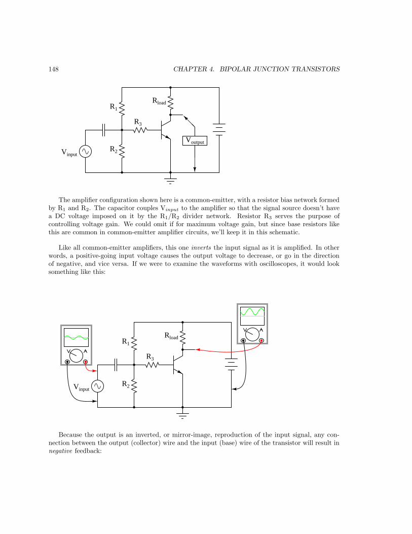
148 CHAPTER 4. BIPOLAR JUNCTION TRANSISTORS
Rload
Vinput
R1
R2
R3
Voutput
The amplifier configuration shown here is a common-emitter, with a resistor bias network formedby R1 and R2. The capacitor couples Vinput to the amplifier so that the signal source doesn’t havea DC voltage imposed on it by the R1/R2 divider network. Resistor R3 serves the purpose ofcontrolling voltage gain. We could omit if for maximum voltage gain, but since base resistors likethis are common in common-emitter amplifier circuits, we’ll keep it in this schematic.
Like all common-emitter amplifiers, this one inverts the input signal as it is amplified. In otherwords, a positive-going input voltage causes the output voltage to decrease, or go in the directionof negative, and vice versa. If we were to examine the waveforms with oscilloscopes, it would looksomething like this:
Rload
Vinput
R1
R2
R3
Because the output is an inverted, or mirror-image, reproduction of the input signal, any con-nection between the output (collector) wire and the input (base) wire of the transistor will result innegative feedback:

4.10. FEEDBACK 149
Rload
Vinput
R1
R2
R3
Rfeedback
The resistances of R1, R2, R3, and Rfeedback function together as a signal-mixing network sothat the voltage seen at the base of the transistor (in reference to ground) is a weighted average ofthe input voltage and the feedback voltage, resulting in signal of reduced amplitude going into thetransistor. As a result, the amplifier circuit will have reduced voltage gain, but improved linearity(reduced distortion) and increased bandwidth.
A resistor connecting collector to base is not the only way to introduce negative feedback into thisamplifier circuit, though. Another method, although more difficult to understand at first, involvesthe placement of a resistor between the transistor’s emitter terminal and circuit ground, like this:
Rload
Vinput
R1
R2
R3
Rfeedback
A different method of introducingnegative feedback into the circuit
This new feedback resistor drops voltage proportional to the emitter current through the transis-tor, and it does so in such a way as to oppose the input signal’s influence on the base-emitter junctionof the transistor. Let’s take a closer look at the emitter-base junction and see what difference thisnew resistor makes:

150 CHAPTER 4. BIPOLAR JUNCTION TRANSISTORS
Vinput
+
-
Ibase
Iemitter
Icollector
+-
VB-E
With no feedback resistor connecting the emitter to ground, whatever level of input signal(Vinput) makes it through the coupling capacitor and R1/R2/R3 resistor network will be impresseddirectly across the base-emitter junction as the transistor’s input voltage (VB−E). In other words,with no feedback resistor, VB−E equals Vinput. Therefore, if Vinput increases by 100 mV, thenVB−E likewise increases by 100 mV: a change in one is the same as a change in the other, since thetwo voltages are equal to each other.
Now let’s consider the effects of inserting a resistor (Rfeedback) between the transistor’s emitterlead and ground:
Vinput
+
-
Ibase
Iemitter
Icollector
+-
VB-E
Rfeedback
+
-Vfeedback
Note how the voltage dropped across Rfeedback adds with VB−E to equal Vinput. With Rfeedback
in the Vinput −− VB−E loop, VB−E will no longer be equal to Vinput. We know that Rfeedback
will drop a voltage proportional to emitter current, which is in turn controlled by the base current,which is in turn controlled by the voltage dropped across the base-emitter junction of the transistor(VB−E). Thus, if Vinput were to increase in a positive direction, it would increase VB−E , causingmore base current, causing more collector (load) current, causing more emitter current, and causingmore feedback voltage to be dropped across Rfeedback. This increase of voltage drop across thefeedback resistor, though, subtracts from Vinput to reduce the VB−E , so that the actual voltageincrease for VB−E will be less than the voltage increase of Vinput. No longer will a 100 mV increasein Vinput result in a full 100 mV increase for VB−E , because the two voltages are not equal to eachother.
Consequently, the input voltage has less control over the transistor than before, and the voltagegain for the amplifier is reduced: just what we expected from negative feedback.
In practical common-emitter circuits, negative feedback isn’t just a luxury; it’s a necessity forstable operation. In a perfect world, we could build and operate a common-emitter transistoramplifier with no negative feedback, and have the full amplitude of Vinput impressed across the
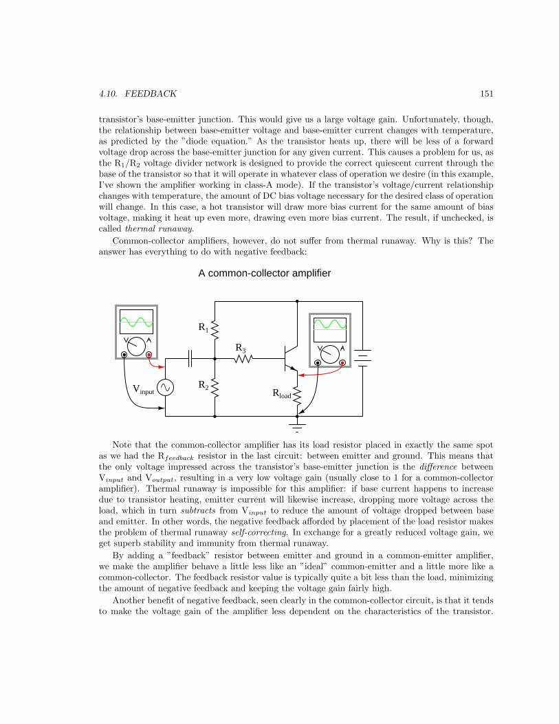
4.10. FEEDBACK 151
transistor’s base-emitter junction. This would give us a large voltage gain. Unfortunately, though,the relationship between base-emitter voltage and base-emitter current changes with temperature,as predicted by the ”diode equation.” As the transistor heats up, there will be less of a forwardvoltage drop across the base-emitter junction for any given current. This causes a problem for us, asthe R1/R2 voltage divider network is designed to provide the correct quiescent current through thebase of the transistor so that it will operate in whatever class of operation we desire (in this example,I’ve shown the amplifier working in class-A mode). If the transistor’s voltage/current relationshipchanges with temperature, the amount of DC bias voltage necessary for the desired class of operationwill change. In this case, a hot transistor will draw more bias current for the same amount of biasvoltage, making it heat up even more, drawing even more bias current. The result, if unchecked, iscalled thermal runaway.
Common-collector amplifiers, however, do not suffer from thermal runaway. Why is this? Theanswer has everything to do with negative feedback:
RloadVinput
R1
R2
R3
A common-collector amplifier
Note that the common-collector amplifier has its load resistor placed in exactly the same spotas we had the Rfeedback resistor in the last circuit: between emitter and ground. This means thatthe only voltage impressed across the transistor’s base-emitter junction is the difference betweenVinput and Voutput, resulting in a very low voltage gain (usually close to 1 for a common-collectoramplifier). Thermal runaway is impossible for this amplifier: if base current happens to increasedue to transistor heating, emitter current will likewise increase, dropping more voltage across theload, which in turn subtracts from Vinput to reduce the amount of voltage dropped between baseand emitter. In other words, the negative feedback afforded by placement of the load resistor makesthe problem of thermal runaway self-correcting. In exchange for a greatly reduced voltage gain, weget superb stability and immunity from thermal runaway.
By adding a ”feedback” resistor between emitter and ground in a common-emitter amplifier,we make the amplifier behave a little less like an ”ideal” common-emitter and a little more like acommon-collector. The feedback resistor value is typically quite a bit less than the load, minimizingthe amount of negative feedback and keeping the voltage gain fairly high.
Another benefit of negative feedback, seen clearly in the common-collector circuit, is that it tendsto make the voltage gain of the amplifier less dependent on the characteristics of the transistor.

152 CHAPTER 4. BIPOLAR JUNCTION TRANSISTORS
Note that in a common-collector amplifier, voltage gain is nearly equal to unity (1), regardless of thetransistor’s β. This means, among other things, that we could replace the transistor in a common-collector amplifier with one having a different β and not see any significant changes in voltage gain.In a common-emitter circuit, the voltage gain is highly dependent on β. If we were to replace thetransistor in a common-emitter circuit with another of differing β, the voltage gain for the amplifierwould change significantly. In a common-emitter amplifier equipped with negative feedback, thevoltage gain will still be dependent upon transistor β to some degree, but not as much as before,making the circuit more predictable despite variations in transistor β.The fact that we have to introduce negative feedback into a common-emitter amplifier to avoid
thermal runaway is an unsatisfying solution. It would be nice, after all, to avoid thermal runawaywithout having to suppress the amplifier’s inherently high voltage gain. A best-of-both-worldssolution to this dilemma is available to us if we closely examine the nature of the problem: thevoltage gain that we have to minimize in order to avoid thermal runaway is the DC voltage gain,not the AC voltage gain. After all, it isn’t the AC input signal that fuels thermal runaway: it’s theDC bias voltage required for a certain class of operation: that quiescent DC signal that we use to”trick” the transistor (fundamentally a DC device) into amplifying an AC signal. We can suppressDC voltage gain in a common-emitter amplifier circuit without suppressing AC voltage gain if wefigure out a way to make the negative feedback function with DC only. That is, if we only feed backan inverted DC signal from output to input, but not an inverted AC signal.The Rfeedback emitter resistor provides negative feedback by dropping a voltage proportional to
load current. In other words, negative feedback is accomplished by inserting an impedance into theemitter current path. If we want to feed back DC but not AC, we need an impedance that is highfor DC but low for AC. What kind of circuit presents a high impedance to DC but a low impedanceto AC? A high-pass filter, of course!By connecting a capacitor in parallel with the feedback resistor, we create the very situation we
need: a path from emitter to ground that is easier for AC than it is for DC:
Rload
Vinput
R1
R2
R3
Rfeedback Cbypass
High AC voltage gain re-establishedby adding Cbypass in parallel with Rfeedback
The new capacitor ”bypasses” AC from the transistor’s emitter to ground, so that no appreciableAC voltage will be dropped from emitter to ground to ”feed back” to the input and suppress voltagegain. Direct current, on the other hand, cannot go through the bypass capacitor, and so must travel

4.10. FEEDBACK 153
through the feedback resistor, dropping a DC voltage between emitter and ground which lowers theDC voltage gain and stabilizes the amplifier’s DC response, preventing thermal runaway. Because wewant the reactance of this capacitor (XC) to be as low as possible, Cbypass should be sized relativelylarge. Because the polarity across this capacitor will never change, it is safe to use a polarized(electrolytic) capacitor for the task.
Another approach to the problem of negative feedback reducing voltage gain is to use multi-stage amplifiers rather than single-transistor amplifiers. If the attenuated gain of a single transistoris insufficient for the task at hand, we can use more than one transistor to make up for the reductioncaused by feedback. Here is an example circuit showing negative feedback in a three-stage common-emitter amplifier:
VinputVoutput
Rin
Rfeedback
Note how there is but one ”path” for feedback, from the final output to the input through a singleresistor, Rfeedback. Since each stage is a common-emitter amplifier – and thus inverting in nature– and there are an odd number of stages from input to output, the output signal will be invertedwith respect to the input signal, and the feedback will be negative (degenerative). Relatively largeamounts of feedback may be used without sacrificing voltage gain, because the three amplifier stagesprovide so much gain to begin with.
At first, this design philosophy may seem inelegant and perhaps even counter-productive. Isn’tthis a rather crude way to overcome the loss in gain incurred through the use of negative feedback,to simply recover gain by adding stage after stage? What is the point of creating a huge voltagegain using three transistor stages if we’re just going to attenuate all that gain anyway with negativefeedback? The point, though perhaps not apparent at first, is increased predictability and stabilityfrom the circuit as a whole. If the three transistor stages are designed to provide an arbitrarily highvoltage gain (in the tens of thousands, or greater) with no feedback, it will be found that the additionof negative feedback causes the overall voltage gain to become less dependent of the individual stagegains, and approximately equal to the simple ratio Rfeedback/Rin. The more voltage gain the circuithas (without feedback), the more closely the voltage gain will approximate Rfeedback/Rin oncefeedback is established. In other words, voltage gain in this circuit is fixed by the values of tworesistors, and nothing more.
This advantage has profound impact on mass-production of electronic circuitry: if amplifiersof predictable gain may be constructed using transistors of widely varied β values, it makes theselection and replacement of components very easy and inexpensive. It also means the amplifier’sgain varies little with changes in temperature. This principle of stable gain control through a high-gain amplifier ”tamed” by negative feedback is elevated almost to an art form in electronic circuits

154 CHAPTER 4. BIPOLAR JUNCTION TRANSISTORS
called operational amplifiers, or op-amps. You may read much more about these circuits in a laterchapter of this book!
• REVIEW:
• Feedback is the coupling of an amplifier’s output to its input.
• Positive, or regenerative feedback has the tendency of making an amplifier circuit unstable, sothat it produces oscillations (AC). The frequency of these oscillations is largely determined bythe components in the feedback network.
• Negative, or degenerative feedback has the tendency of making an amplifier circuit more stable,so that its output changes less for a given input signal than without feedback. This reduces thegain of the amplifier, but has the advantage of decreasing distortion and increasing bandwidth(the range of frequencies the amplifier can handle).
• Negative feedback may be introduced into a common-emitter circuit by coupling collector tobase, or by inserting a resistor between emitter and ground.
• An emitter-to-ground ”feedback” resistor is usually found in common-emitter circuits as apreventative measure against thermal runaway.
• Negative feedback also has the advantage of making amplifier voltage gain more dependent onresistor values and less dependent on the transistor’s characteristics.
• Common-collector amplifiers have a lot of negative feedback, due to the placement of the loadresistor between emitter and ground. This feedback accounts for the extremely stable voltagegain of the amplifier, as well as its immunity against thermal runaway.
• Voltage gain for a common-emitter circuit may be re-established without sacrificing immunityto thermal runaway, by connecting a bypass capacitor in parallel with the emitter ”feedbackresistor.”
• If the voltage gain of an amplifier is arbitrarily high (tens of thousands, or greater), andnegative feedback is used to reduce the gain to reasonable levels, it will be found that the gainwill approximately equal Rfeedback/Rin. Changes in transistor β or other internal componentvalues will have comparatively little effect on voltage gain with feedback in operation, resultingin an amplifier that is stable and easy to design.
4.11 Amplifier impedances
*** PENDING ***
• REVIEW:
•
•
•

4.12. CURRENT MIRRORS 155
4.12 Current mirrors
An interesting and often-used circuit applying the bipolar junction transistor is the so-called currentmirror, which serves as a simple current regulator, supplying nearly constant current to a load overa wide range of load resistances.
We know that in a transistor operating in its active mode, collector current is equal to basecurrent multiplied by the ratio β. We also know that the ratio between collector current and emittercurrent is called α. Because collector current is equal to base current multiplied by β, and emittercurrent is the sum of the base and collector currents, α should be mathematically derivable from β.If you do the algebra, you’ll find that α = β/(β+1) for any transistor.
We’ve seen already how maintaining a constant base current through an active transistor resultsin the regulation of collector current, according to the β ratio. Well, the α ratio works similarly: ifemitter current is held constant, collector current will remain at a stable, regulated value so longas the transistor has enough collector-to-emitter voltage drop to maintain it in its active mode.Therefore, if we have a way of holding emitter current constant through a transistor, the transistorwill work to regulate collector current at a constant value.
Remember that the base-emitter junction of a BJT is nothing more than a PN junction, just likea diode, and that the ”diode equation” specifies how much current will go through a PN junctiongiven forward voltage drop and junction temperature:
ID = IS (eqVD/NkT - 1)
Where,
ID = Diode current in amps
IS = Saturation current in amps
e = Euler’s constant (~ 2.718281828)q = charge of electron (1.6 x 10⁻¹⁹ coulombs)
VD = Voltage applied across diode in volts
N = "Nonideality" or "emission" coefficient
(typically 1 x 10-12 amps)
(typically between 1 and 2)
T = Junction temperature in degrees Kelvin
k = Boltzmann’s constant (1.38 x 10⁻²³)
If both junction voltage and temperature are held constant, then the PN junction current willlikewise be constant. Following this rationale, if we were to hold the base-emitter voltage of a tran-sistor constant, then its emitter current should likewise be constant, given a constant temperature:

156 CHAPTER 4. BIPOLAR JUNCTION TRANSISTORS
Rload
Vbase(constant)
(constant)
β (constant)
Icollector(constant)
Ibase
Iemitter(constant)
α (constant)
This constant emitter current, multiplied by a constant α ratio, gives a constant collector currentthrough Rload, provided that there is enough battery voltage to keep the transistor in its active modefor any change in Rload’s resistance.
Maintaining a constant voltage across the transistor’s base-emitter junction is easy: use aforward-biased diode to establish a constant voltage of approximately 0.7 volts, and connect itin parallel with the base-emitter junction:
Rload
(constant)
Ibase(constant)
β (constant)
Icollector(constant)
0.7 V Idiode(constant)
Iemitter(constant)
α (constant)
Rbias
Now, here’s where it gets interesting. The voltage dropped across the diode probably won’t be0.7 volts exactly. The exact amount of forward voltage dropped across it depends on the currentthrough the diode, and the diode’s temperature, all in accordance with the diode equation. Ifdiode current is increased (say, by reducing the resistance of Rbias), its voltage drop will increaseslightly, increasing the voltage drop across the transistor’s base-emitter junction, which will increasethe emitter current by the same proportion, assuming the diode’s PN junction and the transistor’sbase-emitter junction are well-matched to each other. In other words, transistor emitter currentwill closely equal diode current at any given time. If you change the diode current by changing theresistance value of Rbias, then the transistor’s emitter current will follow suit, because the emittercurrent is described by the same equation as the diode’s, and both PN junctions experience the samevoltage drop.
Remember, the transistor’s collector current is almost equal to its emitter current, as the α ratioof a typical transistor is almost unity (1). If we have control over the transistor’s emitter currentby setting diode current with a simple resistor adjustment, then we likewise have control over thetransistor’s collector current. In other words, collector current mimics, or mirrors, diode current.
Current through resistor Rload is therefore a function of current set by the bias resistor, the two

4.12. CURRENT MIRRORS 157
being nearly equal. This is the function of the current mirror circuit: to regulate current through theload resistor by conveniently adjusting the value of Rbias. It is very easy to create a set amount ofdiode current, as current through the diode is described by a simple equation: power supply voltageminus diode voltage (almost a constant value), divided by the resistance of Rbias.To better match the characteristics of the two PN junctions (the diode junction and the transistor
base-emitter junction), a transistor may be used in place of a regular diode, like this:
RloadRbias
A current mirror circuitusing two transistors
Because temperature is a factor in the ”diode equation,” and we want the two PN junctions tobehave identically under all operating conditions, we should maintain the two transistors at exactlythe same temperature. This is easily done using discrete components by gluing the two transistorcases back-to-back. If the transistors are manufactured together on a single chip of silicon (as aso-called integrated circuit, or IC ), the designers should locate the two transistors very close to oneanother to facilitate heat transfer between them.The current mirror circuit shown with two NPN transistors is sometimes called a current-sinking
type, because the regulating transistor conducts current to the load from ground (”sinking” current),rather than from the positive side of the battery (”sourcing” current). If we wish to have a groundedload, and a current sourcing mirror circuit, we could use PNP transistors like this:
RloadRbias
A current-sourcing mirror circuit
• REVIEW:

158 CHAPTER 4. BIPOLAR JUNCTION TRANSISTORS
• A current mirror is a transistor circuit that regulates current through a load resistance, theregulation point being set by a simple resistor adjustment.
• Transistors in a current mirror circuit must be maintained at the same temperature for pre-cise operation. When using discrete transistors, you may glue their cases together to helpaccomplish this.
• Current mirror circuits may be found in two basic varieties: the current sinking configuration,where the regulating transistor connects the load to ground; and the current sourcing config-uration, where the regulating transistor connects the load to the positive terminal of the DCpower supply.
4.13 Transistor ratings and packages
*** INCOMPLETE ***Like all electrical and electronic components, transistors are limited in the amounts of voltage
and current they can handle without sustaining damage. Since transistors are a bit more complexthan some of the other components you’re used to seeing at this point, they tend to have more kindsof ratings. What follows is an itemized description of some typical transistor ratings.Power dissipation: When a transistor conducts current between collector and emitter, it also
drops voltage between those two points. At any given time, the power dissipated by a transistoris equal to the product (multiplication) of collector current and collector-emitter voltage. Justlike resistors, transistors are rated in terms of how many watts they can safely dissipate withoutsustaining damage. High temperature is the mortal enemy of all semiconductor devices, and bipolartransistors tend to be more susceptible to thermal damage than most. Power ratings are alwaysgiven in reference to the temperature of ambient (surrounding) air. When transistors are to beused in hotter-than-normal environments, their power ratings must be derated to avoid a shortenedservice life.Reverse voltages: As with diodes, bipolar transistors are rated for maximum allowable reverse-
bias voltage across their PN junctions. This includes voltage ratings for the base-emitter junction,base-collector junction, and also from collector to emitter. The rating for maximum collector-emittervoltage can be thought of in terms of the maximum voltage it can withstand while in full-cutoff mode(no base current). This rating is of particular importance when using a bipolar transistor as a switch.Collector current : A maximum value for collector current will be given by the manufacturer in
amps. Understand that this maximum figure assumes a saturated state (minimum collector-emittervoltage drop). If the transistor is not saturated, and in fact is dropping substantial voltage betweencollector and emitter, the maximum power dissipation rating will probably be exceeded before themaximum collector current rating will. Just something to keep in mind when designing a transistorcircuit!Saturation voltages: Ideally, a saturated transistor acts as a closed switch contact between col-
lector and emitter, dropping zero voltage at full collector current. In reality this is never true.Manufacturers will specify the maximum voltage drop of a transistor at saturation, both betweenthe collector and emitter, and also between base and emitter (forward voltage drop of that PNjunction). Collector-emitter voltage drop at saturation is generally expected to be 0.3 volts or less,but this figure is of course dependent on the specific type of transistor. Base-emitter forward voltagedrop is very similar to that of an equivalent diode, which should come as no surprise.

4.14. BJT QUIRKS 159
Beta: The ratio of collector current to base current, β is the fundamental parameter character-izing the amplifying ability of a bipolar transistor. β is usually assumed to be a constant figurein circuit calculations, but unfortunately this is far from true in practice. As such, manufacturersprovide a set of β (or ”hfe”) figures for a given transistor over a wide range of operating conditions,usually in the form of maximum/minimum/typical ratings. It may surprise you to see just howwidely β can be expected to vary within normal operating limits. One popular small-signal tran-sistor, the 2N3903, is advertised as having a β ranging from 15 to 150 depending on the amount ofcollector current. Generally, β is highest for medium collector currents, decreasing for very low andvery high collector currents.Alpha: the ratio of collector current to emitter current, α may be derived from β, being equal to
β/(β+1).Bipolar transistors come in a wide variety of physical packages. Package type is primarily de-
pendent upon the power dissipation of the transistor, much like resistors: the greater the maximumpower dissipation, the larger the device has to be to stay cool. There are several standardized pack-age types for three-terminal semiconductor devices, any of which may be used to house a bipolartransistor. This is an important fact to consider: there are many other semiconductor devices otherthan bipolar transistors which have three connection points. It is impossible to positively identifya three-terminal semiconductor device without referencing the part number printed on it, and/orsubjecting it to a set of electrical tests.
• REVIEW:
•
•
•
4.14 BJT quirks
*** PENDING ***Nonlinearity Temperature drift Thermal runaway Junction capacitance Noise Mismatch (problem
with paralleling transistors) β cutoff frequency Alpha cutoff frequency
• REVIEW:
•
•
•

160 CHAPTER 4. BIPOLAR JUNCTION TRANSISTORS

Chapter 5
JUNCTION FIELD-EFFECTTRANSISTORS
Contents
5.1 Introduction . . . . . . . . . . . . . . . . . . . . . . . . . . . . . . . . . . 161
5.2 The transistor as a switch . . . . . . . . . . . . . . . . . . . . . . . . . . 163
5.3 Meter check of a transistor . . . . . . . . . . . . . . . . . . . . . . . . . 166
5.4 Active-mode operation . . . . . . . . . . . . . . . . . . . . . . . . . . . . 168
5.5 The common-source amplifier – PENDING . . . . . . . . . . . . . . . 177
5.6 The common-drain amplifier – PENDING . . . . . . . . . . . . . . . . 178
5.7 The common-gate amplifier – PENDING . . . . . . . . . . . . . . . . . 178
5.8 Biasing techniques – PENDING . . . . . . . . . . . . . . . . . . . . . . 178
5.9 Transistor ratings and packages – PENDING . . . . . . . . . . . . . . 178
5.10 JFET quirks – PENDING . . . . . . . . . . . . . . . . . . . . . . . . . . 179
*** INCOMPLETE ***
5.1 Introduction
A transistor is a linear semiconductor device that controls current with the application of a lower-power electrical signal. Transistors may be roughly grouped into two major divisions: bipolar andfield-effect. In the last chapter we studied bipolar transistors, which utilize a small current to controla large current. In this chapter, we’ll introduce the general concept of the field-effect transistor –a device utilizing a small voltage to control current – and then focus on one particular type: thejunction field-effect transistor. In the next chapter we’ll explore another type of field-effect transistor,the insulated gate variety.All field-effect transistors are unipolar rather than bipolar devices. That is, the main current
through them is comprised either of electrons through an N-type semiconductor or holes through aP-type semiconductor. This becomes more evident when a physical diagram of the device is seen:
161

162 CHAPTER 5. JUNCTION FIELD-EFFECT TRANSISTORS
schematic symbol physical diagram
P Ngate
drain
source
drain
source
gate
N-channel JFET
In a junction field-effect transistor, or JFET, the controlled current passes from source to drain,or from drain to source as the case may be. The controlling voltage is applied between the gateand source. Note how the current does not have to cross through a PN junction on its way betweensource and drain: the path (called a channel) is an uninterrupted block of semiconductor material.In the image just shown, this channel is an N-type semiconductor. P-type channel JFETs are alsomanufactured:
schematic symbol physical diagram
PNgate
drain
source
drain
source
gate
P-channel JFET
Generally, N-channel JFETs are more commonly used than P-channel. The reasons for this haveto do with obscure details of semiconductor theory, which I’d rather not discuss in this chapter. Aswith bipolar transistors, I believe the best way to introduce field-effect transistor usage is to avoidtheory whenever possible and concentrate instead on operational characteristics. The only practicaldifference between N- and P-channel JFETs you need to concern yourself with now is biasing of thePN junction formed between the gate material and the channel.With no voltage applied between gate and source, the channel is a wide-open path for electrons to
flow. However, if a voltage is applied between gate and source of such polarity that it reverse-biasesthe PN junction, the flow between source and drain connections becomes limited, or regulated, justas it was for bipolar transistors with a set amount of base current. Maximum gate-source voltage

5.2. THE TRANSISTOR AS A SWITCH 163
”pinches off” all current through source and drain, thus forcing the JFET into cutoff mode. Thisbehavior is due to the depletion region of the PN junction expanding under the influence of a reverse-bias voltage, eventually occupying the entire width of the channel if the voltage is great enough.This action may be likened to reducing the flow of a liquid through a flexible hose by squeezing it:with enough force, the hose will be constricted enough to completely block the flow.
waterhose nozzle
Hose constricted by squeezing,water flow reduced or stopped
water
Note how this operational behavior is exactly opposite of the bipolar junction transistor. Bipolartransistors are normally-off devices: no current through the base, no current through the collectoror the emitter. JFETs, on the other hand, are normally-on devices: no voltage applied to the gateallows maximum current through the source and drain. Also take note that the amount of currentallowed through a JFET is determined by a voltage signal rather than a current signal as with bipolartransistors. In fact, with the gate-source PN junction reverse-biased, there should be nearly zerocurrent through the gate connection. For this reason, we classify the JFET as a voltage-controlleddevice, and the bipolar transistor as a current-controlled device.If the gate-source PN junction is forward-biased with a small voltage, the JFET channel will
”open” a little more to allow greater currents through. However, the PN junction of a JFET is notbuilt to handle any substantial current itself, and thus it is not recommended to forward-bias thejunction under any circumstances.This is a very condensed overview of JFET operation. In the next section, we’ll explore the use
of the JFET as a switching device.
5.2 The transistor as a switch
Like its bipolar cousin, the field-effect transistor may be used as an on/off switch controlling electricalpower to a load. Let’s begin our investigation of the JFET as a switch with our familiar switch/lampcircuit:
switch

164 CHAPTER 5. JUNCTION FIELD-EFFECT TRANSISTORS
Remembering that the controlled current in a JFET flows between source and drain, we substitutethe source and drain connections of a JFET for the two ends of the switch in the above circuit:
If you haven’t noticed by now, the source and drain connections on a JFET look identical on theschematic symbol. Unlike the bipolar junction transistor where the emitter is clearly distinguishedfrom the collector by the arrowhead, a JFET’s source and drain lines both run perpendicular intothe bar representing the semiconductor channel. This is no accident, as the source and drain linesof a JFET are often interchangeable in practice! In other words, JFETs are usually able to handlechannel current in either direction, from source to drain or from drain to source.
Now all we need in the circuit is a way to control the JFET’s conduction. With zero appliedvoltage between gate and source, the JFET’s channel will be ”open,” allowing full current to thelamp. In order to turn the lamp off, we will need to connect another source of DC voltage betweenthe gate and source connections of the JFET like this:
switch
Closing this switch will ”pinch off” the JFET’s channel, thus forcing it into cutoff and turningthe lamp off:
switch
Note that there is no current going through the gate. As a reverse-biased PN junction, it firmlyopposes the flow of any electrons through it. As a voltage-controlled device, the JFET requiresnegligible input current. This is an advantageous trait of the JFET over the bipolar transistor:there is virtually zero power required of the controlling signal.
Opening the control switch again should disconnect the reverse-biasing DC voltage from the gate,thus allowing the transistor to turn back on. Ideally, anyway, this is how it works. In practice thismay not work at all:
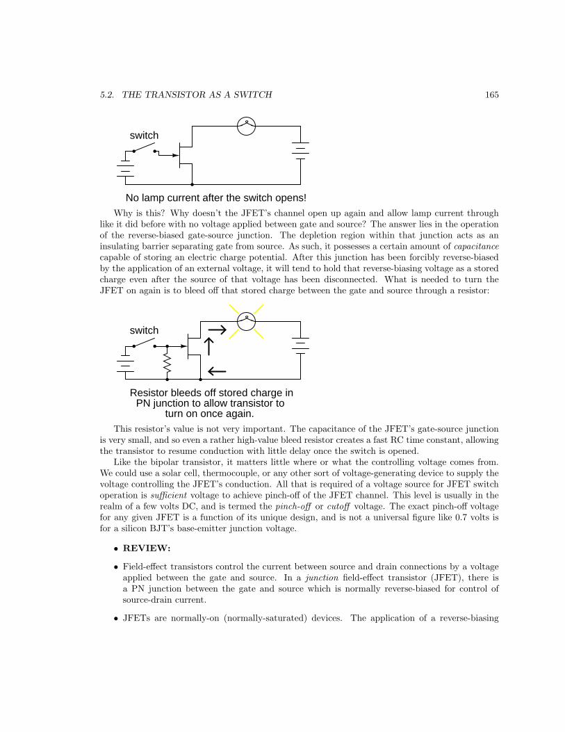
5.2. THE TRANSISTOR AS A SWITCH 165
switch
No lamp current after the switch opens!Why is this? Why doesn’t the JFET’s channel open up again and allow lamp current through
like it did before with no voltage applied between gate and source? The answer lies in the operationof the reverse-biased gate-source junction. The depletion region within that junction acts as aninsulating barrier separating gate from source. As such, it possesses a certain amount of capacitancecapable of storing an electric charge potential. After this junction has been forcibly reverse-biasedby the application of an external voltage, it will tend to hold that reverse-biasing voltage as a storedcharge even after the source of that voltage has been disconnected. What is needed to turn theJFET on again is to bleed off that stored charge between the gate and source through a resistor:
switch
Resistor bleeds off stored charge inPN junction to allow transistor to
turn on once again.This resistor’s value is not very important. The capacitance of the JFET’s gate-source junction
is very small, and so even a rather high-value bleed resistor creates a fast RC time constant, allowingthe transistor to resume conduction with little delay once the switch is opened.Like the bipolar transistor, it matters little where or what the controlling voltage comes from.
We could use a solar cell, thermocouple, or any other sort of voltage-generating device to supply thevoltage controlling the JFET’s conduction. All that is required of a voltage source for JFET switchoperation is sufficient voltage to achieve pinch-off of the JFET channel. This level is usually in therealm of a few volts DC, and is termed the pinch-off or cutoff voltage. The exact pinch-off voltagefor any given JFET is a function of its unique design, and is not a universal figure like 0.7 volts isfor a silicon BJT’s base-emitter junction voltage.
• REVIEW:
• Field-effect transistors control the current between source and drain connections by a voltageapplied between the gate and source. In a junction field-effect transistor (JFET), there isa PN junction between the gate and source which is normally reverse-biased for control ofsource-drain current.
• JFETs are normally-on (normally-saturated) devices. The application of a reverse-biasing
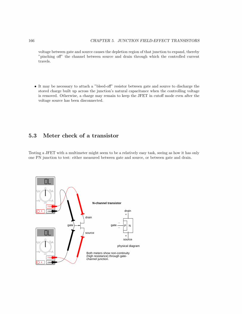
166 CHAPTER 5. JUNCTION FIELD-EFFECT TRANSISTORS
voltage between gate and source causes the depletion region of that junction to expand, thereby”pinching off” the channel between source and drain through which the controlled currenttravels.
• It may be necessary to attach a ”bleed-off” resistor between gate and source to discharge thestored charge built up across the junction’s natural capacitance when the controlling voltageis removed. Otherwise, a charge may remain to keep the JFET in cutoff mode even after thevoltage source has been disconnected.
5.3 Meter check of a transistor
Testing a JFET with a multimeter might seem to be a relatively easy task, seeing as how it has onlyone PN junction to test: either measured between gate and source, or between gate and drain.
COMA
V
V A
AOFF
COMA
V
V A
AOFF
+
-
+
-
N-channel transistor
gate
drain
source
physical diagram
P Ngate
drain
source
Both meters show non-continuity(high resistance) through gate-channel junction.

5.3. METER CHECK OF A TRANSISTOR 167
COMA
V
V A
AOFF
COMA
V
V A
AOFF
+
-
+
-
N-channel transistor
gate
drain
source
physical diagram
P Ngate
drain
source
Both meters show continuity (lowresistance) through gate-channeljunction.
Testing continuity through the drain-source channel is another matter, though. Remember fromthe last section how a stored charge across the capacitance of the gate-channel PN junction couldhold the JFET in a pinched-off state without any external voltage being applied across it? Thiscan occur even when you’re holding the JFET in your hand to test it! Consequently, any meterreading of continuity through that channel will be unpredictable, since you don’t necessarily knowif a charge is being stored by the gate-channel junction. Of course, if you know beforehand whichterminals on the device are the gate, source, and drain, you may connect a jumper wire betweengate and source to eliminate any stored charge and then proceed to test source-drain continuitywith no problem. However, if you don’t know which terminals are which, the unpredictability of thesource-drain connection may confuse your determination of terminal identity.
A good strategy to follow when testing a JFET is to insert the pins of the transistor into anti-static foam (the material used to ship and store static-sensitive electronic components) just prior totesting. The conductivity of the foam will make a resistive connection between all terminals of thetransistor when it is inserted. This connection will ensure that all residual voltage built up acrossthe gate-channel PN junction will be neutralized, thus ”opening up” the channel for an accuratemeter test of source-to-drain continuity.
Since the JFET channel is a single, uninterrupted piece of semiconductor material, there is usuallyno difference between the source and drain terminals. A resistance check from source to drain shouldyield the same value as a check from drain to source. This resistance should be relatively low (a fewhundred ohms at most) when the gate-source PN junction voltage is zero. By applying a reverse-bias voltage between gate and source, pinch-off of the channel should be apparent by an increasedresistance reading on the meter.

168 CHAPTER 5. JUNCTION FIELD-EFFECT TRANSISTORS
5.4 Active-mode operation
JFETs, like bipolar transistors, are able to ”throttle” current in a mode between cutoff and saturationcalled the active mode. To better understand JFET operation, let’s set up a SPICE simulationsimilar to the one used to explore basic bipolar transistor function:
V1Q1
Vammeter
0 V
1
0 0 0
2 3
Vin
jfet simulation
vin 0 1 dc 1
j1 2 1 0 mod1
vammeter 3 2 dc 0
v1 3 0 dc
.model mod1 njf
.dc v1 0 2 0.05
.plot dc i(vammeter)
.end
Note that the transistor labeled ”Q1” in the schematic is represented in the SPICE netlist asj1. Although all transistor types are commonly referred to as ”Q” devices in circuit schematics –just as resistors are referred to by ”R” designations, and capacitors by ”C” – SPICE needs to betold what type of transistor this is by means of a different letter designation: q for bipolar junctiontransistors, and j for junction field-effect transistors.

5.4. ACTIVE-MODE OPERATION 169
Here, the controlling signal is a steady voltage of 1 volt, applied with negative towards theJFET gate and positive toward the JFET source, to reverse-bias the PN junction. In the first BJTsimulation of chapter 4, a constant-current source of 20 µA was used for the controlling signal, butremember that a JFET is a voltage-controlled device, not a current-controlled device like the bipolarjunction transistor.
Like the BJT, the JFET tends to regulate the controlled current at a fixed level above a certainpower supply voltage, no matter how high that voltage may climb. Of course, this current regulationhas limits in real life – no transistor can withstand infinite voltage from a power source – and withenough drain-to-source voltage the transistor will ”break down” and drain current will surge. Butwithin normal operating limits the JFET keeps the drain current at a steady level independent ofpower supply voltage. To verify this, we’ll run another computer simulation, this time sweeping thepower supply voltage (V1) all the way to 50 volts:
jfet simulation
vin 0 1 dc 1
j1 2 1 0 mod1
vammeter 3 2 dc 0
v1 3 0 dc
.model mod1 njf
.dc v1 0 50 2
.plot dc i(vammeter)
.end
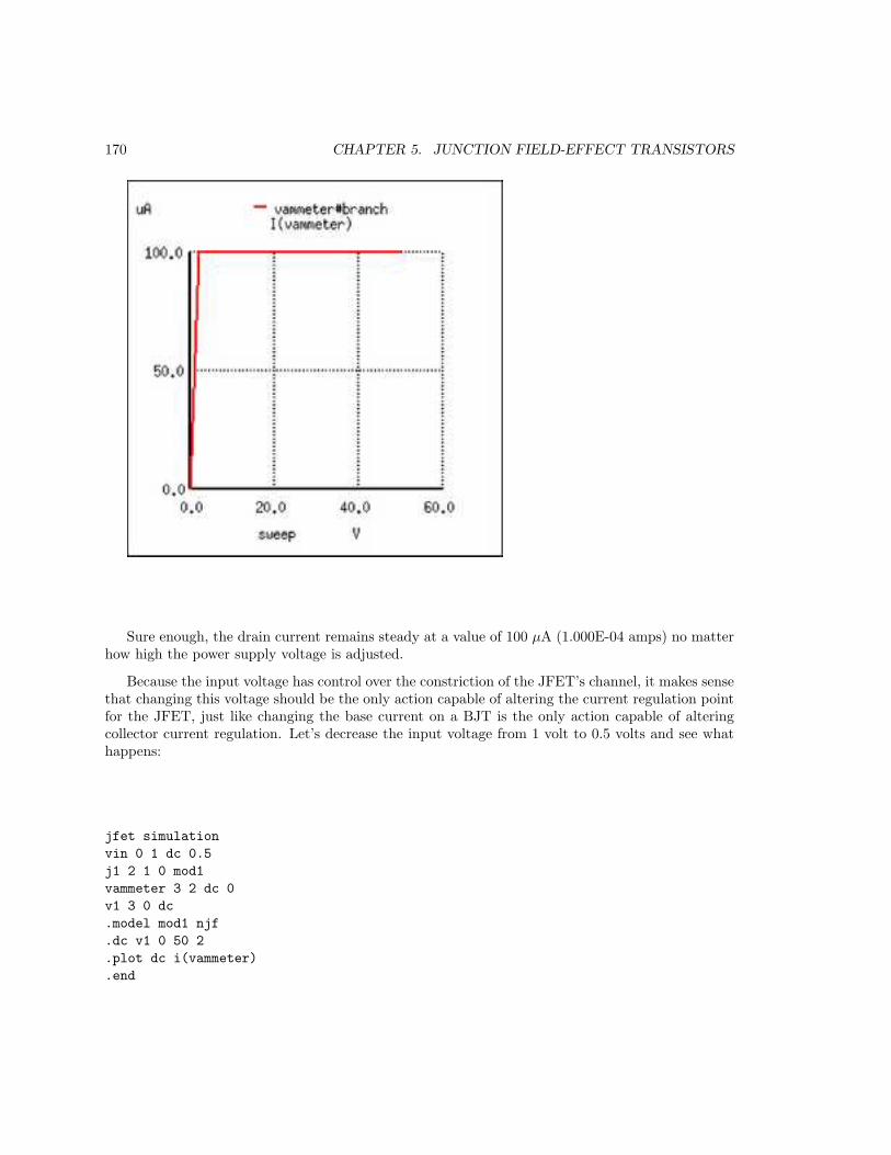
170 CHAPTER 5. JUNCTION FIELD-EFFECT TRANSISTORS
Sure enough, the drain current remains steady at a value of 100 µA (1.000E-04 amps) no matterhow high the power supply voltage is adjusted.
Because the input voltage has control over the constriction of the JFET’s channel, it makes sensethat changing this voltage should be the only action capable of altering the current regulation pointfor the JFET, just like changing the base current on a BJT is the only action capable of alteringcollector current regulation. Let’s decrease the input voltage from 1 volt to 0.5 volts and see whathappens:
jfet simulation
vin 0 1 dc 0.5
j1 2 1 0 mod1
vammeter 3 2 dc 0
v1 3 0 dc
.model mod1 njf
.dc v1 0 50 2
.plot dc i(vammeter)
.end
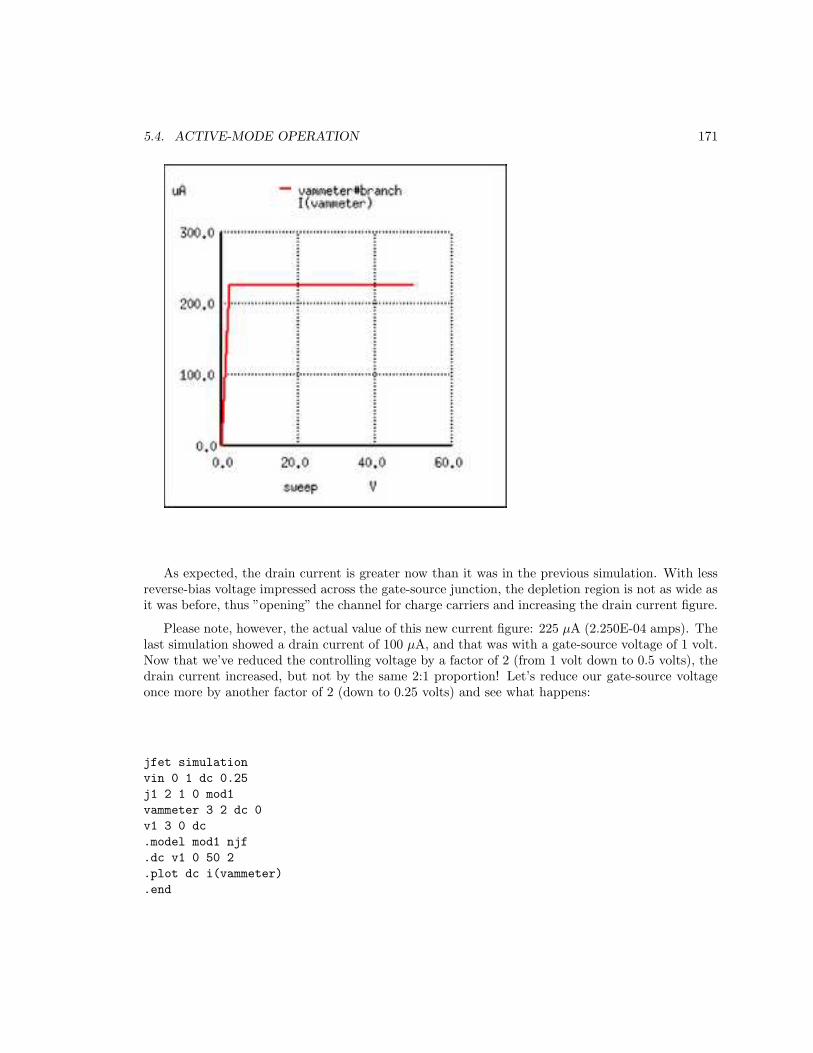
5.4. ACTIVE-MODE OPERATION 171
As expected, the drain current is greater now than it was in the previous simulation. With lessreverse-bias voltage impressed across the gate-source junction, the depletion region is not as wide asit was before, thus ”opening” the channel for charge carriers and increasing the drain current figure.
Please note, however, the actual value of this new current figure: 225 µA (2.250E-04 amps). Thelast simulation showed a drain current of 100 µA, and that was with a gate-source voltage of 1 volt.Now that we’ve reduced the controlling voltage by a factor of 2 (from 1 volt down to 0.5 volts), thedrain current increased, but not by the same 2:1 proportion! Let’s reduce our gate-source voltageonce more by another factor of 2 (down to 0.25 volts) and see what happens:
jfet simulation
vin 0 1 dc 0.25
j1 2 1 0 mod1
vammeter 3 2 dc 0
v1 3 0 dc
.model mod1 njf
.dc v1 0 50 2
.plot dc i(vammeter)
.end

172 CHAPTER 5. JUNCTION FIELD-EFFECT TRANSISTORS
With the gate-source voltage set to 0.25 volts, one-half what it was before, the drain currentis 306.3 µA. Although this is still an increase over the 225 µA from the prior simulation, it isn’tproportional to the change of the controlling voltage.
To obtain a better understanding of what is going on here, we should run a different kind ofsimulation: one that keeps the power supply voltage constant and instead varies the controlling(voltage) signal. When this kind of simulation was run on a BJT, the result was a straight-linegraph, showing how the input current / output current relationship of a BJT is linear. Let’s seewhat kind of relationship a JFET exhibits:
jfet simulation
vin 0 1 dc
j1 2 1 0 mod1
vammeter 3 2 dc 0
v1 3 0 dc 25
.model mod1 njf
.dc vin 0 2 0.1
.plot dc i(vammeter)
.end

5.4. ACTIVE-MODE OPERATION 173
This simulation directly reveals an important characteristic of the junction field-effect transistor:the control effect of gate voltage over drain current is nonlinear. Notice how the drain current doesnot decrease linearly as the gate-source voltage is increased. With the bipolar junction transistor,collector current was directly proportional to base current: output signal proportionately followedinput signal. Not so with the JFET! The controlling signal (gate-source voltage) has less and lesseffect over the drain current as it approaches cutoff. In this simulation, most of the controlling action(75 percent of drain current decrease – from 400 µA to 100 µA) takes place within the first volt ofgate-source voltage (from 0 to 1 volt), while the remaining 25 percent of drain current reductiontakes another whole volt worth of input signal. Cutoff occurs at 2 volts input.
Linearity is generally important for a transistor because it allows it to faithfully amplify a wave-form without distorting it. If a transistor is nonlinear in its input/output amplification, the shape ofthe input waveform will become corrupted in some way, leading to the production of harmonics inthe output signal. The only time linearity is not important in a transistor circuit is when it’s beingoperated at the extreme limits of cutoff and saturation (off and on, respectively, like a switch).
A JFET’s characteristic curves display the same current-regulating behavior as for a BJT, andthe nonlinearity between gate-to-source voltage and drain current is evident in the disproportionatevertical spacings between the curves:

174 CHAPTER 5. JUNCTION FIELD-EFFECT TRANSISTORS
Idrain
Edrain-to-source
Vgate-to-source =
Vgate-to-source =
Vgate-to-source =
0 V
1 V
2 V = VP (pinch-off)
Vgate-to-source = 0.5 V
|VDS| = |VP| - |VGS|
Above pinch-offBelow pinch-off
Saturation region
Ohmic region
Triode region
To better comprehend the current-regulating behavior of the JFET, it might be helpful to drawa model made up of simpler, more common components, just as we did for the BJT:
G
S
D
N-channel JFET diode-regulating diode model
S
D
G
In the case of the JFET, it is the voltage across the reverse-biased gate-source diode which setsthe current regulation point for the pair of constant-current diodes. A pair of opposing constant-current diodes is included in the model to facilitate current in either direction between source and

5.4. ACTIVE-MODE OPERATION 175
drain, a trait made possible by the unipolar nature of the channel. With no PN junctions for thesource-drain current to traverse, there is no polarity sensitivity in the controlled current. For thisreason, JFETs are often referred to as bilateral devices.
A contrast of the JFET’s characteristic curves against the curves for a bipolar transistor revealsa notable difference: the linear (straight) portion of each curve’s non-horizontal area is surprisinglylong compared to the respective portions of a BJT’s characteristic curves:
Idrain
Edrain-to-source
Vgate-to-source =
Vgate-to-source =
Vgate-to-source =
0 V
1 V
2 V (pinch-off)
Vgate-to-source = 0.5 V
"Ohmic regions"
Icollector
Ecollector-to-emitter
Ibase = 75 µA
Ibase = 40 µA
Ibase = 20 µA
Ibase = 5 µA
A JFET transistor operated in the triode region tends to act very much like a plain resistor asmeasured from drain to source. Like all simple resistances, its current/voltage graph is a straightline. For this reason, the triode region (non-horizontal) portion of a JFET’s characteristic curveis sometimes referred to as the ohmic region. In this mode of operation where there isn’t enough

176 CHAPTER 5. JUNCTION FIELD-EFFECT TRANSISTORS
drain-to-source voltage to bring drain current up to the regulated point, the drain current is directlyproportional to the drain-to-source voltage. In a carefully designed circuit, this phenomenon can beused to an advantage. Operated in this region of the curve, the JFET acts like a voltage-controlledresistance rather than a voltage-controlled current regulator, and the appropriate model for thetransistor is different:
N-channel JFET diode-rheostat model(for saturation, or "ohmic," mode only!)
G
D
S
S
D
G
Here and here alone the rheostat (variable resistor) model of a transistor is accurate. It mustbe remembered, however, that this model of the transistor holds true only for a narrow range ofits operation: when it is extremely saturated (far less voltage applied between drain and sourcethan what is needed to achieve full regulated current through the drain). The amount of resistance(measured in ohms) between drain and source in this mode is controlled by how much reverse-biasvoltage is applied between gate and source. The less gate-to-source voltage, the less resistance(steeper line on graph).
Because JFETs are voltage-controlled current regulators (at least when they’re allowed to operatein their active), their inherent amplification factor cannot be expressed as a unitless ratio as withBJTs. In other words, there is no β ratio for a JFET. This is true for all voltage-controlled activedevices, including other types of field-effect transistors and even electron tubes. There is, however,an expression of controlled (drain) current to controlling (gate-source) voltage, and it is calledtransconductance. Its unit is Siemens, the same unit for conductance (formerly known as the mho).
Why this choice of units? Because the equation takes on the general form of current (outputsignal) divided by voltage (input signal).
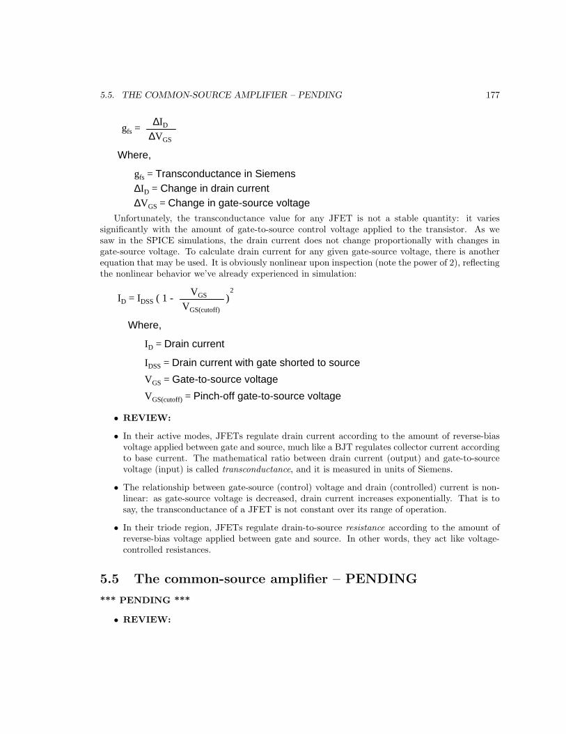
5.5. THE COMMON-SOURCE AMPLIFIER – PENDING 177
Where,
gfs = Transconductance in Siemens
gfs =∆ID
∆VGS
∆ID = Change in drain current∆VGS = Change in gate-source voltage
Unfortunately, the transconductance value for any JFET is not a stable quantity: it variessignificantly with the amount of gate-to-source control voltage applied to the transistor. As wesaw in the SPICE simulations, the drain current does not change proportionally with changes ingate-source voltage. To calculate drain current for any given gate-source voltage, there is anotherequation that may be used. It is obviously nonlinear upon inspection (note the power of 2), reflectingthe nonlinear behavior we’ve already experienced in simulation:
ID = IDSS ( 1 - VGS
VGS(cutoff)
)2
Where,
ID = Drain current
IDSS = Drain current with gate shorted to source
VGS = Gate-to-source voltage
VGS(cutoff) = Pinch-off gate-to-source voltage
• REVIEW:
• In their active modes, JFETs regulate drain current according to the amount of reverse-biasvoltage applied between gate and source, much like a BJT regulates collector current accordingto base current. The mathematical ratio between drain current (output) and gate-to-sourcevoltage (input) is called transconductance, and it is measured in units of Siemens.
• The relationship between gate-source (control) voltage and drain (controlled) current is non-linear: as gate-source voltage is decreased, drain current increases exponentially. That is tosay, the transconductance of a JFET is not constant over its range of operation.
• In their triode region, JFETs regulate drain-to-source resistance according to the amount ofreverse-bias voltage applied between gate and source. In other words, they act like voltage-controlled resistances.
5.5 The common-source amplifier – PENDING
*** PENDING ***
• REVIEW:

178 CHAPTER 5. JUNCTION FIELD-EFFECT TRANSISTORS
•
•
•
5.6 The common-drain amplifier – PENDING
*** PENDING ***
• REVIEW:
•
•
•
5.7 The common-gate amplifier – PENDING
*** PENDING ***
• REVIEW:
•
•
•
5.8 Biasing techniques – PENDING
*** PENDING ***
• REVIEW:
•
•
•
5.9 Transistor ratings and packages – PENDING
*** PENDING ***
• REVIEW:
•
•
•

5.10. JFET QUIRKS – PENDING 179
5.10 JFET quirks – PENDING
*** PENDING ***
• REVIEW:
•
•
•

180 CHAPTER 5. JUNCTION FIELD-EFFECT TRANSISTORS

Chapter 6
INSULATED-GATEFIELD-EFFECT TRANSISTORS
Contents
6.1 Introduction . . . . . . . . . . . . . . . . . . . . . . . . . . . . . . . . . . 181
6.2 Depletion-type IGFETs . . . . . . . . . . . . . . . . . . . . . . . . . . . . 182
6.3 Enhancement-type IGFETs – PENDING . . . . . . . . . . . . . . . . . 192
6.4 Active-mode operation – PENDING . . . . . . . . . . . . . . . . . . . . 192
6.5 The common-source amplifier – PENDING . . . . . . . . . . . . . . . 193
6.6 The common-drain amplifier – PENDING . . . . . . . . . . . . . . . . 193
6.7 The common-gate amplifier – PENDING . . . . . . . . . . . . . . . . . 193
6.8 Biasing techniques – PENDING . . . . . . . . . . . . . . . . . . . . . . 193
6.9 Transistor ratings and packages – PENDING . . . . . . . . . . . . . . 193
6.10 IGFET quirks – PENDING . . . . . . . . . . . . . . . . . . . . . . . . . 194
6.11 MESFETs – PENDING . . . . . . . . . . . . . . . . . . . . . . . . . . . 194
6.12 IGBTs . . . . . . . . . . . . . . . . . . . . . . . . . . . . . . . . . . . . . . 194
*** INCOMPLETE ***
6.1 Introduction
As was stated in the last chapter, there is more than one type of field-effect transistor. The junctionfield-effect transistor, or JFET, uses voltage applied across a reverse-biased PN junction to controlthe width of that junction’s depletion region, which then controls the conductivity of a semiconduc-tor channel through which the controlled current moves. Another type of field-effect device – theinsulated gate field-effect transistor, or IGFET – exploits a similar principle of a depletion regioncontrolling conductivity through a semiconductor channel, but it differs primarily from the JFETin that there is no direct connection between the gate lead and the semiconductor material itself.Rather, the gate lead is insulated from the transistor body by a thin barrier, hence the term insulated
181

182 CHAPTER 6. INSULATED-GATE FIELD-EFFECT TRANSISTORS
gate. This insulating barrier acts like the dielectric layer of a capacitor, and allows gate-to-sourcevoltage to influence the depletion region electrostatically rather than by direct connection.
In addition to a choice of N-channel versus P-channel design, IGFETs come in two major types:enhancement and depletion. The depletion type is more closely related to the JFET, so we willbegin our study of IGFETs with it.
6.2 Depletion-type IGFETs
Insulated gate field-effect transistors are unipolar devices just like JFETs: that is, the controlledcurrent does not have to cross a PN junction. There is a PN junction inside the transistor, butits only purpose is to provide that nonconducting depletion region which is used to restrict currentthrough the channel.
Here is a diagram of an N-channel IGFET of the ”depletion” type:
schematic symbol physical diagram
PNgate
drain
source
drain
source
gatesubstrate
N-channel, D-type IGFET
insulatingbarrier
substrate
Notice how the source and drain leads connect to either end of the N channel, and how the gatelead attaches to a metal plate separated from the channel by a thin insulating barrier. That barrieris sometimes made from silicon dioxide (the primary chemical compound found in sand), whichis a very good insulator. Due to this Metal (gate) - Oxide (barrier) - Semiconductor (channel)construction, the IGFET is sometimes referred to as a MOSFET. There are other types of IGFETconstruction, though, and so ”IGFET” is the better descriptor for this general class of transistors.
Notice also how there are four connections to the IGFET. In practice, the substrate lead is directlyconnected to the source lead to make the two electrically common. Usually, this connection is madeinternally to the IGFET, eliminating the separate substrate connection, resulting in a three-terminaldevice with a slightly different schematic symbol:
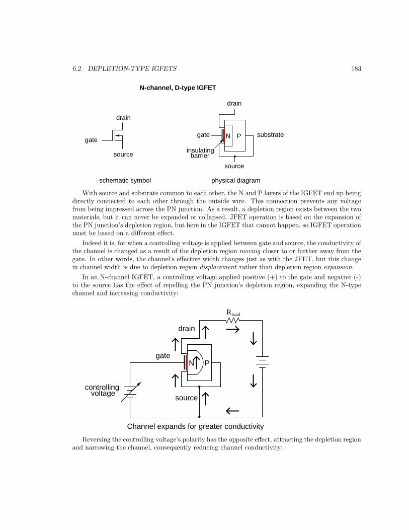
6.2. DEPLETION-TYPE IGFETS 183
schematic symbol physical diagram
PNgate
drain
source
drain
source
gate
N-channel, D-type IGFET
insulatingbarrier
substrate
With source and substrate common to each other, the N and P layers of the IGFET end up beingdirectly connected to each other through the outside wire. This connection prevents any voltagefrom being impressed across the PN junction. As a result, a depletion region exists between the twomaterials, but it can never be expanded or collapsed. JFET operation is based on the expansion ofthe PN junction’s depletion region, but here in the IGFET that cannot happen, so IGFET operationmust be based on a different effect.
Indeed it is, for when a controlling voltage is applied between gate and source, the conductivity ofthe channel is changed as a result of the depletion region moving closer to or further away from thegate. In other words, the channel’s effective width changes just as with the JFET, but this changein channel width is due to depletion region displacement rather than depletion region expansion.
In an N-channel IGFET, a controlling voltage applied positive (+) to the gate and negative (-)to the source has the effect of repelling the PN junction’s depletion region, expanding the N-typechannel and increasing conductivity:
PNgate
drain
source
Rload
controllingvoltage
Channel expands for greater conductivity
Reversing the controlling voltage’s polarity has the opposite effect, attracting the depletion regionand narrowing the channel, consequently reducing channel conductivity:

184 CHAPTER 6. INSULATED-GATE FIELD-EFFECT TRANSISTORS
PNgate
drain
source
Rload
controllingvoltage
Channel narrows for less conductivity
The insulated gate allows for controlling voltages of any polarity without danger of forward-biasing a junction, as was the concern with JFETs. This type of IGFET, although it’s called a”depletion-type,” actually has the capability of having its channel either depleted (channel narrowed)or enhanced (channel expanded). Input voltage polarity determines which way the channel will beinfluenced.
Understanding which polarity has which effect is not as difficult as it may seem. The key isto consider the type of semiconductor doping used in the channel (N-channel or P-channel?), thenrelate that doping type to the side of the input voltage source connected to the channel by means ofthe source lead. If the IGFET is an N-channel and the input voltage is connected so that the positive(+) side is on the gate while the negative (-) side is on the source, the channel will be enhanced asextra electrons build up on the channel side of the dielectric barrier. Think, ”negative (-) correlateswith N -type, thus enhancing the channel with the right type of charge carrier (electrons) and makingit more conductive.” Conversely, if the input voltage is connected to an N-channel IGFET the otherway, so that negative (-) connects to the gate while positive (+) connects to the source, free electronswill be ”robbed” from the channel as the gate-channel capacitor charges, thus depleting the channelof majority charge carriers and making it less conductive.
For P-channel IGFETs, the input voltage polarity and channel effects follow the same rule. Thatis to say, it takes just the opposite polarity as an N-channel IGFET to either deplete or enhance:

6.2. DEPLETION-TYPE IGFETS 185
P Ngate
drain
source
Rload
controllingvoltage
Channel expands for greater conductivity
PN
gate
drain
source
Rload
controllingvoltage
Channel narrows for less conductivity
Illustrating the proper biasing polarities with standard IGFET symbols:

186 CHAPTER 6. INSULATED-GATE FIELD-EFFECT TRANSISTORS
N-channel P-channel
Enhanced(more drain
current)
Depleted(less draincurrent)
+
-
+
- +
-
+
-
When there is zero voltage applied between gate and source, the IGFET will conduct currentbetween source and drain, but not as much current as it would if it were enhanced by the propergate voltage. This places the depletion-type, or simply D-type, IGFET in a category of its own in thetransistor world. Bipolar junction transistors are normally-off devices: with no base current, theyblock any current from going through the collector. Junction field-effect transistors are normally-ondevices: with zero applied gate-to-source voltage, they allow maximum drain current (actually, youcan coax a JFET into greater drain currents by applying a very small forward-bias voltage betweengate and source, but this should never be done in practice for risk of damaging its fragile PNjunction). D-type IGFETs, however, are normally half-on devices: with no gate-to-source voltage,their conduction level is somewhere between cutoff and full saturation. Also, they will tolerateapplied gate-source voltages of any polarity, the PN junction being immune from damage due to theinsulating barrier and especially the direct connection between source and substrate preventing anyvoltage differential across the junction.
Ironically, the conduction behavior of a D-type IGFET is strikingly similar to that of an electrontube of the triode/tetrode/pentode variety. These devices were voltage-controlled current regulatorsthat likewise allowed current through them with zero controlling voltage applied. A controllingvoltage of one polarity (grid negative and cathode positive) would diminish conductivity throughthe tube while a voltage of the other polarity (grid positive and cathode negative) would enhanceconductivity. I find it curious that one of the later transistor designs invented exhibits the samebasic properties of the very first active (electronic) device.
A few SPICE analyses will demonstrate the current-regulating behavior of D-type IGFETs. First,a test with zero input voltage (gate shorted to source) and the power supply swept from 0 to 50volts. The graph shows drain current:

6.2. DEPLETION-TYPE IGFETS 187
Q1V1
Vammeter
0 V
0
0
0
1 2
n-channel igfet characteristic curve
m1 1 0 0 0 mod1
vammeter 2 1 dc 0
v1 2 0
.model mod1 nmos vto=-1
.dc v1 0 50 2
.plot dc i(vammeter)
.end
As expected for any transistor, the controlled current holds steady at a regulated value over awide range of power supply voltages. In this case, that regulated point is 10 µA (1.000E-05). Now

188 CHAPTER 6. INSULATED-GATE FIELD-EFFECT TRANSISTORS
let’s see what happens when we apply a negative voltage to the gate (with reference to the source)and sweep the power supply over the same range of 0 to 50 volts:
Q1V1
Vammeter
0 V
0 0
1 2
3
0.5 V
n-channel igfet characteristic curve
m1 1 3 0 0 mod1
vin 0 3 dc 0.5
vammeter 2 1 dc 0
v1 2 0
.model mod1 nmos vto=-1
.dc v1 0 50 2
.plot dc i(vammeter)
.end

6.2. DEPLETION-TYPE IGFETS 189
Not surprisingly, the drain current is now regulated at a lower value of 2.5 µA (down from 10µA with zero input voltage). Now let’s apply an input voltage of the other polarity, to enhance theIGFET:
Q1V1
Vammeter
0 V
0 0
1 2
3
0.5 V
n-channel igfet characteristic curve
m1 1 3 0 0 mod1
vin 3 0 dc 0.5
vammeter 2 1 dc 0
v1 2 0
.model mod1 nmos vto=-1
.dc v1 0 50 2
.plot dc i(vammeter)
.end

190 CHAPTER 6. INSULATED-GATE FIELD-EFFECT TRANSISTORS
With the transistor enhanced by the small controlling voltage, the drain current is now at anincreased value of 22.5 µA (2.250E-05). It should be apparent from these three sets of voltage andcurrent figures that the relationship of drain current to gate-source voltage is nonlinear just as itwas with the JFET. With 1/2 volt of depleting voltage, the drain current is 2.5 µA; with 0 voltsinput the drain current goes up to 10 µA; and with 1/2 volt of enhancing voltage, the current isat 22.5 µA. To obtain a better understanding of this nonlinearity, we can use SPICE to plot thedrain current over a range of input voltage values, sweeping from a negative (depleting) figure to apositive (enhancing) figure, maintaining the power supply voltage of V1 at a constant value:
n-channel igfet
m1 1 3 0 0 mod1
vin 3 0
vammeter 2 1 dc 0
v1 2 0 dc 24
.model mod1 nmos vto=-1
.dc vin -1 1 0.1
.plot dc i(vammeter)
.end

6.2. DEPLETION-TYPE IGFETS 191
Just as it was with JFETs, this inherent nonlinearity of the IGFET has the potential to causedistortion in an amplifier circuit, as the input signal will not be reproduced with 100 percent accuracyat the output. Also notice that a gate-source voltage of about 1 volt in the depleting direction isable to pinch off the channel so that there is virtually no drain current. D-type IGFETs, like JFETs,have a certain pinch-off voltage rating. This rating varies with the precise unique of the transistor,and may not be the same as in our simulation here.
Plotting a set of characteristic curves for the IGFET, we see a pattern not unlike that of theJFET:

192 CHAPTER 6. INSULATED-GATE FIELD-EFFECT TRANSISTORS
Idrain
Edrain-to-source
Vgate-to-source =
Vgate-to-source =
0 VVgate-to-source =
-0.5 V
+0.5 V
• REVIEW:
•
•
•
6.3 Enhancement-type IGFETs – PENDING
• REVIEW:
•
•
•
6.4 Active-mode operation – PENDING
• REVIEW:
•
•
•

6.5. THE COMMON-SOURCE AMPLIFIER – PENDING 193
6.5 The common-source amplifier – PENDING
• REVIEW:
•
•
•
6.6 The common-drain amplifier – PENDING
• REVIEW:
•
•
•
6.7 The common-gate amplifier – PENDING
• REVIEW:
•
•
•
6.8 Biasing techniques – PENDING
• REVIEW:
•
•
•
6.9 Transistor ratings and packages – PENDING
• REVIEW:
•
•
•

194 CHAPTER 6. INSULATED-GATE FIELD-EFFECT TRANSISTORS
6.10 IGFET quirks – PENDING
• REVIEW:
•
•
•
6.11 MESFETs – PENDING
• REVIEW:
•
•
•
6.12 IGBTs
Because of their insulated gates, IGFETs of all types have extremely high current gain: there can beno sustained gate current if there is no continuous gate circuit in which electrons may continuallyflow. The only current we see through the gate terminal of an IGFET, then, is whatever transient(brief surge) may be required to charge the gate-channel capacitance and displace the depletionregion as the transistor switches from an ”on” state to an ”off” state, or vice versa.This high current gain would at first seem to place IGFET technology at a decided advantage
over bipolar transistors for the control of very large currents. If a bipolar junction transistor is usedto control a large collector current, there must be a substantial base current sourced or sunk bysome control circuitry, in accordance with the β ratio. To give an example, in order for a powerBJT with a β of 20 to conduct a collector current of 100 amps, there must be at least 5 amps ofbase current, a substantial amount of current in itself for miniature discrete or integrated controlcircuitry to handle:
β = 20
Rload
100 A
105 A
Controlcircuitry
5 A

6.12. IGBTS 195
It would be nice from the standpoint of control circuitry to have power transistors with highcurrent gain, so that far less current is needed for control of load current. Of course, we can useDarlington pair transistors to increase the current gain, but this kind of arrangement still requiresfar more controlling current than an equivalent power IGFET:
β = 20
Rload
100 A
105 A
Controlcircuitry
5 A
0.238 A
Rload
100 A
Controlcircuitry
100 A
≈ 0 A
Unfortunately, though, IGFETs have problems of their own controlling high current: they typi-cally exhibit greater drain-to-source voltage drop while saturated than the collector-to-emitter volt-age drop of a saturated BJT. This greater voltage drop equates to higher power dissipation for thesame amount of load current, limiting the usefulness of IGFETs as high-power devices. Althoughsome specialized designs such as the so-called VMOS transistor have been designed to minimize thisinherent disadvantage, the bipolar junction transistor is still superior in its ability to switch highcurrents.
An interesting solution to this dilemma leverages the best features of IGFETs with the best offeatures of BJTs, in one device called an Insulated-Gate Bipolar Transistor, or IGBT. Also knownas an Bipolar-mode MOSFET, a Conductivity-Modulated Field-Effect Transistor (COMFET ), orsimply as an Insulated-Gate Transistor (IGT ), it is equivalent to a Darlington pair of IGFET andBJT:

196 CHAPTER 6. INSULATED-GATE FIELD-EFFECT TRANSISTORS
Insulated-Gate Bipolar Transistor (IGBT)
Schematic symbols Equivalent circuit
(N-channel)
Collector
Gate
Emitter
CollectorCollector
EmitterEmitterGate
Gate
In essence, the IGFET controls the base current of a BJT, which handles the main load currentbetween collector and emitter. This way, there is extremely high current gain (since the insulatedgate of the IGFET draws practically no current from the control circuitry), but the collector-to-emitter voltage drop during full conduction is as low as that of an ordinary BJT.One disadvantage of the IGBT over a standard BJT is its slower turn-off time. For fast switching
and high current-handling capacity, it’s difficult to beat the bipolar junction transistor. Faster turn-off times for the IGBT may be achieved by certain changes in design, but only at the expense of ahigher saturated voltage drop between collector and emitter. However, the IGBT provides a goodalternative to IGFETs and BJTs for high-power control applications.
• REVIEW:
•
•
•

Chapter 7
THYRISTORS
Contents
7.1 Hysteresis . . . . . . . . . . . . . . . . . . . . . . . . . . . . . . . . . . . . 197
7.2 Gas discharge tubes . . . . . . . . . . . . . . . . . . . . . . . . . . . . . . 198
7.3 The Shockley Diode . . . . . . . . . . . . . . . . . . . . . . . . . . . . . . 202
7.4 The DIAC . . . . . . . . . . . . . . . . . . . . . . . . . . . . . . . . . . . . 208
7.5 The Silicon-Controlled Rectifier (SCR) . . . . . . . . . . . . . . . . . . 209
7.6 The TRIAC . . . . . . . . . . . . . . . . . . . . . . . . . . . . . . . . . . . 220
7.7 Optothyristors . . . . . . . . . . . . . . . . . . . . . . . . . . . . . . . . . 222
7.8 The Unijunction Transistor (UJT) – PENDING . . . . . . . . . . . . . 223
7.9 The Silicon-Controlled Switch (SCS) . . . . . . . . . . . . . . . . . . . . 223
7.10 Field-effect-controlled thyristors . . . . . . . . . . . . . . . . . . . . . . 225
*** INCOMPLETE ***
7.1 Hysteresis
Thyristors are a class of semiconductor components exhibiting hysteresis, that property whereby asystem fails to return to its original state after some cause of state change has been removed. A verysimple example of hysteresis is the mechanical action of a toggle switch: when the lever is pushed, itflips to one of two extreme states (positions) and will remain there even after the source of motion isremoved (after you remove your hand from the switch lever). To illustrate the absence of hysteresis,consider the action of a ”momentary” pushbutton switch, which returns to its original state afterthe button is no longer pressed: when the stimulus is removed (your hand), the system (switch)immediately and fully returns to its prior state with no ”latching” behavior.Bipolar, junction field-effect, and insulated gate field-effect transistors are all non-hysteretic de-
vices. That is, they do not inherently ”latch” into a state after being stimulated by a voltage orcurrent signal. For any given input signal at any given time, a transistor will exhibit a predictableoutput response as defined by its characteristic curve. Thyristors, on the other hand, are semicon-ductor devices that tend to stay ”on” once turned on, and tend to stay ”off” once turned off. A
197

198 CHAPTER 7. THYRISTORS
momentary event is able to flip these devices into either their on or off states where they will remainthat way on their own, even after the cause of the state change is taken away. As such, they areuseful only as on/off switching devices – much like a toggle switch – and cannot be used as analogsignal amplifiers.Thyristors are constructed using the same technology as bipolar junction transistors, and in fact
may be analyzed as circuits comprised of transistor pairs. How then, can a hysteretic device (athyristor) be made from non-hysteretic devices (transistors)? The answer to this question is positivefeedback, also known as regenerative feedback. As you should recall, feedback is the condition wherea percentage of the output signal is ”fed back” to the input of an amplifying device. Negative, ordegenerative, feedback results in a diminishing of voltage gain with increases in stability, linearity,and bandwidth. Positive feedback, on the other hand, results in a kind of instability where theamplifier’s output tends to ”saturate.” In the case of thyristors, this saturating tendency equates tothe device ”wanting” to stay on once turned on, and off once turned off.In this chapter we will explore several different kinds of thyristors, most of which stem from a
single, basic two-transistor core circuit. Before we do that, though, it would be beneficial to studythe technological predecessor to thyristors: gas discharge tubes.
7.2 Gas discharge tubes
If you’ve ever witnessed a lightning storm, you’ve seen electrical hysteresis in action (and probablydidn’t realize what you were seeing). The action of strong wind and rain accumulates tremendousstatic electric charges between cloud and earth, and between clouds as well. Electric charge imbal-ances manifest themselves as high voltages, and when the electrical resistance of air can no longerhold these high voltages at bay, huge surges of current travel between opposing poles of electricalcharge which we call ”lightning.”The buildup of high voltages by wind and rain is a fairly continuous process, the rate of charge
accumulation increasing under the proper atmospheric conditions. However, lightning bolts areanything but continuous: they exist as relatively brief surges rather than continuous discharges.Why is this? Why don’t we see soft, glowing lightning arcs instead of violently brief lightning bolts?The answer lies in the nonlinear (and hysteretic) resistance of air.Under ordinary conditions, air has an extremely high amount of resistance. It is so high, in
fact, that we typically treat its resistance as infinite and electrical conduction through the air asnegligible. The presence of water and/or dust in air lowers its resistance some, but it is still aninsulator for most practical purposes. When a sufficient amount of high voltage is applied acrossa distance of air, though, its electrical properties change: electrons become ”stripped” from theirnormal positions around their respective atoms and are liberated to constitute a current. In thisstate, air is considered to be ionized and is referred to as a plasma rather than a normal gas. Thisusage of the word ”plasma” is not to be confused with the medical term (meaning the fluid portionof blood), but is a fourth state of matter, the other three being solid, liquid, and vapor (gas). Plasmais a relatively good conductor of electricity, its specific resistance being much lower than that of thesame substance in its gaseous state.As an electric current moves through the plasma, there is energy dissipated in the plasma in
the form of heat, just as current through a solid resistor dissipates energy in the form of heat. Inthe case of lightning, the temperatures involved are extremely high. High temperatures are alsosufficient to convert gaseous air into a plasma or maintain plasma in that state without the presence

7.2. GAS DISCHARGE TUBES 199
of high voltage. As the voltage between cloud and earth, or between cloud and cloud, decreases asthe charge imbalance is neutralized by the current of the lightning bolt, the heat dissipated by thebolt maintains the air path in a plasma state, keeping its resistance low. The lightning bolt remainsa plasma until the voltage decreases to too low a level to sustain enough current to dissipate enoughheat. Finally, the air returns to a normal, gaseous state and stops conducting current, thus allowingvoltage to build up once more.
Note how throughout this cycle, the air exhibits hysteresis. When not conducting electricity, ittends to remain an insulator until voltage builds up past a critical threshold point. Then, once itchanges state and becomes a plasma, it tends to remain a conductor until voltage falls below a lowercritical threshold point. Once ”turned on” it tends to stay ”on,” and once ”turned off” it tends tostay ”off.” This hysteresis, combined with a steady buildup of voltage due to the electrostatic effectsof wind and rain, explains the action of lightning as brief bursts.
In electronic terms, what we have here in the action of lightning is a simple relaxation oscillator.Oscillators are electronic circuits that produce an oscillating (AC) voltage from a steady supply ofDC power. A relaxation oscillator is one that works on the principle of a charging capacitor thatis suddenly discharged every time its voltage reaches a critical threshold value. One of the simplestrelaxation oscillators in existence is comprised of three components (not counting the DC powersupply): a resistor, capacitor, and neon lamp:
R
C Neon lamp
Simple relaxation oscillator
Neon lamps are nothing more than two metal electrodes inside a sealed glass bulb, separated bythe neon gas inside. At room temperatures and with no applied voltage, the lamp has nearly infiniteresistance. However, once a certain threshold voltage is exceeded (this voltage depends on the gaspressure and geometry of the lamp), the neon gas will become ionized (turned into a plasma) andits resistance dramatically reduced. In effect, the neon lamp exhibits the same characteristics as airin a lightning storm, complete with the emission of light as a result of the discharge, albeit on amuch smaller scale.
The capacitor in the relaxation oscillator circuit shown above charges at an inverse exponentialrate determined by the size of the resistor. When its voltage reaches the threshold voltage of thelamp, the lamp suddenly ”turns on” and quickly discharges the capacitor to a low voltage value.Once discharged, the lamp ”turns off” and allows the capacitor to build up a charge once more. Theresult is a series of brief flashes of light from the lamp, the rate of which dictated by battery voltage,resistor resistance, capacitor capacitance, and lamp threshold voltage.
While gas-discharge lamps are more commonly used as sources of illumination, their hysteretic

200 CHAPTER 7. THYRISTORS
properties were leveraged in slightly more sophisticated variants known as thyratron tubes. Es-sentially a gas-filled triode tube (a triode being a three-element vacuum electron tube performingmuch a similar function to the N-channel, D-type IGFET), the thyratron tube could be turnedon with a small control voltage applied between grid and cathode, and turned off by reducing theplate-to-cathode voltage.
Rload
controlvoltage
ThyratronTube high voltage
AC source
+
-
(Simple) Thyratron control circuit
In essence, thyratron tubes were controlled versions of neon lamps built specifically for switchingcurrent to a load. The dot inside the circle of the schematic symbol indicates a gas fill, as opposedto the hard vacuum normally seen in other electron tube designs. In the circuit shown above, thethyratron tube allows current through the load in one direction (note the polarity across the loadresistor) when triggered by the small DC control voltage connected between grid and cathode. Notethat the load’s power source is AC, which provides a clue as to how the thyratron turns off afterit’s been triggered on: since AC voltage periodically passes through a condition of 0 volts betweenhalf-cycles, the current through an AC-powered load must also periodically halt. This brief pauseof current between half-cycles gives the tube’s gas time to cool, letting it return to its normal ”off”state. Conduction may resume only if there is enough voltage applied by the AC power source (someother time in the wave’s cycle) and if the DC control voltage allows it.An oscilloscope display of load voltage in such a circuit would look something like this:
AC supply voltage
Load voltage
Threshold voltage
As the AC supply voltage climbs from zero volts to its first peak, the load voltage remains atzero (no load current) until the threshold voltage is reached. At that point, the tube switches ”on”

7.2. GAS DISCHARGE TUBES 201
and begins to conduct, the load voltage now following the AC voltage through the rest of the halfcycle. Notice how there is load voltage (and thus load current) even when the AC voltage waveformhas dropped below the threshold value of the tube. This is hysteresis at work: the tube stays in itsconductive mode past the point where it first turned on, continuing to conduct until there the supplyvoltage drops off to almost zero volts. Because thyratron tubes are one-way (diode) devices, thereis no voltage across the load through the negative half-cycle of AC. In practical thyratron circuits,multiple tubes arranged in some form of full-wave rectifier circuit to facilitate full-wave DC powerto the load.Although I’m not sure if this was ever done, someone could have applied the thyratron tube
to a relaxation oscillator circuit and control the frequency with a small DC voltage between gridand cathode, making a crude voltage-controlled oscillator, otherwise known as a VCO. Relaxationoscillators tend to have poor frequency control, not to mention a very non-sinusoidal output, andso they exist mostly as demonstration circuits (as is the case here) or in applications where precisefrequency control isn’t important. Consequently, this use of a thyratron tube would not have beena very practical one.
R
C
Controllingvoltage
I speak of thyratron tubes in the past tense for good reason: modern semiconductor componentshave obsoleted thyratron tube technology for all but a few very special applications. It is no co-incidence that the word thyristor bears so much similarity to the word thyratron, for this class ofsemiconductor components does much the same thing: use hysteretically switch current on and off.It is these modern devices that we now turn our attention to.
• REVIEW:
• Electrical hysteresis, the tendency for a component to remain ”on” (conducting) after it beginsto conduct and to remain ”off” (nonconducting) after it ceases to conduct, helps to explainwhy lightning bolts exist as momentary surges of current rather than continuous dischargesthrough the air.
• Simple gas-discharge tubes such as neon lamps exhibit electrical hysteresis.
• More advanced gas-discharge tubes have been made with control elements so that their ”turn-on” voltage could be adjusted by an external signal. The most common of these tubes wascalled the thyratron.
• Simple oscillator circuits called relaxation oscillators may be created with nothing more thana resistor-capacitor charging network and a hysteretic device connected across the capacitor.

202 CHAPTER 7. THYRISTORS
7.3 The Shockley Diode
Our exploration of thyristors begins with a device called the four-layer diode, also known as a PNPNdiode, or a Shockley diode after its inventor, William Shockley. This is not to be confused with aSchottky diode, that two-layer metal-semiconductor device known for its high switching speed. Acrude illustration of the Shockley diode, often seen in textbooks, is a four-layer sandwich of P-N-P-Nsemiconductor material:
P
P
N
N
Shockley, or 4-layer,diode
Anode
Cathode
Unfortunately, this simple illustration does nothing to enlighten the viewer on how it works orwhy. Consider an alternative rendering of the device’s construction:
P
P
N
N
Shockley, or 4-layer,diode
Anode
Cathode
N
P
Shown like this, it appears to be a set of interconnected bipolar transistors, one PNP and theother NPN. Drawn using standard schematic symbols, and respecting the layer doping concentrationsnot shown in the last image, the Shockley diode looks like this:

7.3. THE SHOCKLEY DIODE 203
P
P
N
N
Anode
N
P
Cathode Cathode
Anode
Physical diagram Equivalent schematic Schematic symbol
Let’s connect one of these devices to a source of variable voltage and see what happens:
Shockley diodeequivalent circuit
With no voltage applied, of course there will be no current. As voltage is initially increased,there will still be no current because neither transistor is able to turn on: both will be in cutoffmode. To understand why this is, consider what it takes to turn a bipolar junction transistor on:current through the base-emitter junction. As you can see in the diagram, base current throughthe lower transistor is controlled by the upper transistor, and the base current through the uppertransistor is controlled by the lower transistor. In other words, neither transistor can turn on untilthe other transistor turns on. What we have here, in vernacular terms, is known as a Catch-22.
So how can a Shockley diode ever conduct current, if its constituent transistors stubbornlymaintain themselves in a state of cutoff? The answer lies in the behavior of real transistors asopposed to ideal transistors. An ideal bipolar transistor will never conduct collector current if thereis no base current, no matter how much or little voltage we apply between collector and emitter.Real transistors, on the other hand, have definite limits to how much collector-emitter voltage theycan withstand before they break down and conduct. If two real transistors are connected togetherin this fashion to form a Shockley diode, they will be able to conduct if there is sufficient voltageapplied by the battery between anode and cathode to cause one of them to break down. Once onetransistor breaks down and begins to conduct, it will allow base current through the other transistor,causing it to turn on in a normal fashion, which then allows base current through the first transistor.The end result is that both transistors will be saturated, now keeping each other turned on insteadof off.
So, we can force a Shockley diode to turn on by applying sufficient voltage between anode andcathode. As we have seen, this will inevitably cause one of the transistors to turn on, which then turnsthe other transistor on, ultimately ”latching” both transistors on where they will tend to remain.But how do we now get the two transistors to turn off again? Even if the applied voltage is reduced

204 CHAPTER 7. THYRISTORS
to a point well below what it took to get the Shockley diode conducting, it will remain conductingbecause both transistors now have base current to maintain regular, controlled conduction. Theanswer to this is to reduce the applied voltage to a much lower point where there is too little currentto maintain transistor bias, at which point one of the transistors will cutoff, which then halts basecurrent through the other transistor, sealing both transistors in the ”off” state as they were beforeany voltage was applied at all.
If we graph this sequence of events and plot the results on an I/V graph, the hysteresis is veryevident. First, we will observe the circuit as the DC voltage source (battery) is set to zero voltage:
Applied voltage
Circuitcurrent
Zero applied voltage; zero current
Next, we will steadily increase the DC voltage. Current through the circuit is at or nearly atzero, as the breakdown limit has not been reached for either transistor:
Applied voltage
Circuitcurrent
Some voltage applied, still no appreciable current
When the voltage breakdown limit of one transistor is reached, it will begin to conduct collectorcurrent even though no base current has gone through it yet. Normally, this sort of treatmentwould destroy a bipolar junction transistor, but the PNP junctions comprising a Shockley diode areengineered to take this kind of abuse, similar to the way a Zener diode is built to handle reversebreakdown without sustaining damage. For the sake of illustration I’ll assume the lower transistorbreaks down first, sending current through the base of the upper transistor:

7.3. THE SHOCKLEY DIODE 205
Applied voltage
Circuitcurrent
More voltage applied; lower transistor breaks down
As the upper transistor receives base current, it turns on as expected. This action allows thelower transistor to conduct normally, the two transistors ”sealing” themselves in the ”on” state. Fullcurrent is very quickly seen in the circuit:
Applied voltage
Circuitcurrent
Transistors now fully conducting
The positive feedback mentioned earlier in this chapter is clearly evident here. When one tran-sistor breaks down, it allows current through the device structure. This current may be viewed asthe ”output” signal of the device. Once an output current is established, it works to hold bothtransistors in saturation, thus ensuring the continuation of a substantial output current. In otherwords, an output current ”feeds back” positively to the input (transistor base current) to keep bothtransistors in the ”on” state, thus reinforcing (or regenerating) itself.
With both transistors maintained in a state of saturation with the presence of ample base current,they will continue to conduct even if the applied voltage is greatly reduced from the breakdown level.The effect of positive feedback is to keep both transistors in a state of saturation despite the lossof input stimulus (the original, high voltage needed to break down one transistor and cause a basecurrent through the other transistor):

206 CHAPTER 7. THYRISTORS
Applied voltage
Circuitcurrent
Current maintained even when voltage is reduced
If the DC voltage source is turned down too far, though, the circuit will eventually reach a pointwhere there isn’t enough current to sustain both transistors in saturation. As one transistor passesless and less collector current, it reduces the base current for the other transistor, thus reducing basecurrent for the first transistor. The vicious cycle continues rapidly until both transistors fall intocutoff:
Applied voltage
Circuitcurrent
If the voltage drops too low, both transistors shut off
Here, positive feedback is again at work: the fact that the cause/effect cycle between both tran-sistors is ”vicious” (a decrease in current through one works to decrease current through the other,further decreasing current through the first transistor) indicates a positive relationship betweenoutput (controlled current) and input (controlling current through the transistors’ bases).
The resulting curve on the graph is classicly hysteretic: as the input signal (voltage) is increasedand decreased, the output (current) does not follow the same path going down as it did going up:
Applied voltage
Circuitcurrent

7.3. THE SHOCKLEY DIODE 207
Put in simple terms, the Shockley diode tends to stay on once it’s turned on, and stay off onceit’s turned off. There is no ”in-between” or ”active” mode in its operation: it is a purely on or offdevice, as are all thyristors.There are a few special terms applied to Shockley diodes and all other thyristor devices built
upon the Shockley diode foundation. First is the term used to describe its ”on” state: latched. Theword ”latch” is reminiscent of a door lock mechanism, which tends to keep the door closed once ithas been pushed shut. The term firing refers to the initiation of a latched state. In order to get aShockley diode to latch, the applied voltage must be increased until breakover is attained. Despitethe fact that this action is best described in terms of transistor breakdown, the term breakoveris used instead because the end result is a pair of transistors in mutual saturation rather thandestruction as would be the case with a normal transistor. A latched Shockley diode is re-set backinto its nonconducting state by reducing current through it until low-current dropout occurs.It should be noted that Shockley diodes may be fired in a way other than breakover: excessive
voltage rise, or dv/dt. This is when the applied voltage across the diode increases at a high rate ofchange. This is able to cause latching (turning on) of the diode due to inherent junction capacitanceswithin the transistors. Capacitors, as you may recall, oppose changes in voltage by drawing orsupplying current. If the applied voltage across a Shockley diode rises at too fast a rate, thosetiny capacitances will draw enough current during that time to activate the transistor pair, turningthem both on. Usually, this form of latching is undesirable, and can be minimized by filtering high-frequency (fast voltage rises) from the diode with series inductors and/or parallel resistor-capacitornetworks called snubbers:
RC "snubber"
Series inductor
Both the series inductor and the parallelresistor-capacitor "snubber" circuit helpminimize the Shockley diode’s exposureto excessively rising voltages.
Shockleydiode
The voltage rise limit of a Shockley diode is referred to as the critical rate of voltage rise.Manufacturers usually provide this specification for the devices they sell.
• REVIEW:
• Shockley diodes are four-layer PNPN semiconductor devices. They behave as a pair of inter-connected PNP and NPN transistors.

208 CHAPTER 7. THYRISTORS
• Like all thyristors, Shockley diodes tend to stay on once they’ve been turned on (latched), andstay off once they’ve been turned off.
• There are two ways to latch a Shockley diode: exceed the anode-to-cathode breakover voltage,or exceed the anode-to-cathode critical rate of voltage rise.
• There is only one way to cause a Shockley diode to stop conducting, and that is to reduce thecurrent going through it to a level below its low-current dropout threshold.
7.4 The DIAC
Like all diodes, Shockley diodes are unidirectional devices; that is, they only conduct current in onedirection. If bidirectional (AC) operation is desired, two Shockley diodes may be joined in parallelfacing different directions to form a new kind of thyristor, the DIAC :
DIAC equivalent circuit DIAC schematic symbol
A DIAC operated with a DC voltage across it behaves exactly the same as a Shockley diode.With AC, however, the behavior is different from what one might expect. Because alternatingcurrent repeatedly reverses direction, DIACs will not stay latched longer than one-half cycle. If aDIAC becomes latched, it will continue to conduct current only as long as there is voltage availableto push enough current in that direction. When the AC polarity reverses, as it must twice percycle, the DIAC will drop out due to insufficient current, necessitating another breakover before itconducts again. The result is a current waveform that looks like this:
AC supply voltage
DIAC current
Breakover voltage
Breakover voltage
DIACs are almost never used alone, but in conjunction with other thyristor devices.

7.5. THE SILICON-CONTROLLED RECTIFIER (SCR) 209
7.5 The Silicon-Controlled Rectifier (SCR)
Shockley diodes are curious devices, but rather limited in application. Their usefulness may beexpanded, however, by equipping them with another means of latching. In doing so, they becometrue amplifying devices (if only in an on/off mode), and we refer to them as silicon-controlledrectifiers, or SCRs.
The progression from Shockley diode to SCR is achieved with one small addition, actually nothingmore than a third wire connection to the existing PNPN structure:
P
P
N
N
Anode
N
P
Cathode Cathode
Anode
Physical diagram Equivalent schematic Schematic symbol
GateGate
The Silicon-Controlled Rectifier (SCR)
Cathode
Gate
Anode
If an SCR’s gate is left floating (disconnected), it behaves exactly as a Shockley diode. It maybe latched by breakover voltage or by exceeding the critical rate of voltage rise between anode andcathode, just as with the Shockley diode. Dropout is accomplished by reducing current until one orboth internal transistors fall into cutoff mode, also like the Shockley diode. However, because thegate terminal connects directly to the base of the lower transistor, it may be used as an alternativemeans to latch the SCR. By applying a small voltage between gate and cathode, the lower transistorwill be forced on by the resulting base current, which will cause the upper transistor to conduct,which then supplies the lower transistor’s base with current so that it no longer needs to be activatedby a gate voltage. The necessary gate current to initiate latch-up, of course, will be much lowerthan the current through the SCR from cathode to anode, so the SCR does achieve a measure ofamplification.
This method of securing SCR conduction is called triggering, and it is by far the most commonway that SCRs are latched in actual practice. In fact, SCRs are usually chosen so that their breakovervoltage is far beyond the greatest voltage expected to be experienced from the power source, so thatit can be turned on only by an intentional voltage pulse applied to the gate.
It should be mentioned that SCRs may sometimes be turned off by directly shorting their gateand cathode terminals together, or by ”reverse-triggering” the gate with a negative voltage (inreference to the cathode), so that the lower transistor is forced into cutoff. I say this is ”sometimes”possible because it involves shunting all of the upper transistor’s collector current past the lowertransistor’s base. This current may be substantial, making triggered shut-off of an SCR difficult atbest. A variation of the SCR, called a Gate-Turn-Off thyristor, or GTO, makes this task easier.But even with a GTO, the gate current required to turn it off may be as much as 20% of the anode(load) current! The schematic symbol for a GTO is shown in the following illustration:

210 CHAPTER 7. THYRISTORS
Gate Turn-Off thyristor (GTO)
Anode
GateCathode
SCRs and GTOs share the same equivalent schematics (two transistors connected in a positive-feedback fashion), the only differences being details of construction designed to grant the NPNtransistor a greater β than the PNP. This allows a smaller gate current (forward or reverse) to exerta greater degree of control over conduction from cathode to anode, with the PNP transistor’s latchedstate being more dependent upon the NPN’s than vice versa. The Gate-Turn-Off thyristor is alsoknown by the name of Gate-Controlled Switch, or GCS.
A rudimentary test of SCR function, or at least terminal identification, may be performed withan ohmmeter. Because the internal connection between gate and cathode is a single PN junction, ameter should indicate continuity between these terminals with the red test lead on the gate and theblack test lead on the cathode like this:
COMA
V
V A
AOFF
gatecathode
All other continuity measurements performed on an SCR will show ”open” (”OL” on some digitalmultimeter displays). It must be understood that this test is very crude and does not constitute acomprehensive assessment of the SCR. It is possible for an SCR to give good ohmmeter indicationsand still be defective. Ultimately, the only way to test an SCR is to subject it to a load current.
If you are using a multimeter with a ”diode check” function, the gate-to-cathode junction voltageindication you get may or may not correspond to what’s expected of a silicon PN junction (approx-imately 0.7 volts). In some cases, you will read a much lower junction voltage: mere hundredthsof a volt. This is due to an internal resistor connected between the gate and cathode incorporatedwithin some SCRs. This resistor is added to make the SCR less susceptible to false triggering byspurious voltage spikes, from circuit ”noise” or from static electric discharge. In other words, hav-ing a resistor connected across the gate-cathode junction requires that a strong triggering signal(substantial current) be applied to latch the SCR. This feature is often found in larger SCRs, not

7.5. THE SILICON-CONTROLLED RECTIFIER (SCR) 211
on small SCRs. Bear in mind that an SCR with an internal resistor connected between gate andcathode will indicate continuity in both directions between those two terminals:
Cathode
Anode
Gate
Gate-to-Cathoderesistor
”Normal” SCRs, lacking this internal resistor, are sometimes referred to as sensitive gate SCRsdue to their ability to be triggered by the slightest positive gate signal.
The test circuit for an SCR is both practical as a diagnostic tool for checking suspected SCRs andalso an excellent aid to understanding basic SCR operation. A DC voltage source is used for poweringthe circuit, and two pushbutton switches are used to latch and unlatch the SCR, respectively:
SCR undertest
on
off
SCR testing circuit
Actuating the normally-open ”on” pushbutton switch connects the gate to the anode, allowingcurrent from the negative terminal of the battery, through the cathode-gate PN junction, throughthe switch, through the load resistor, and back to the battery. This gate current should force theSCR to latch on, allowing current to go directly from cathode to anode without further triggeringthrough the gate. When the ”on” pushbutton is released, the load should remain energized.
Pushing the normally-closed ”off” pushbutton switch breaks the circuit, forcing current throughthe SCR to halt, thus forcing it to turn off (low-current dropout).
If the SCR fails to latch, the problem may be with the load and not the SCR. There is a certainminimum amount of load current required to hold the SCR latched in the ”on” state. This minimumcurrent level is called the holding current. A load with too great a resistance value may not drawenough current to keep an SCR latched when gate current ceases, thus giving the false impressionof a bad (unlatchable) SCR in the test circuit. Holding current values for different SCRs should

212 CHAPTER 7. THYRISTORS
be available from the manufacturers. Typical holding current values range from 1 milliamp to 50milliamps or more for larger units.For the test to be fully comprehensive, more than the triggering action needs to be tested. The
forward breakover voltage limit of the SCR could be tested by increasing the DC voltage supply(with no pushbuttons actuated) until the SCR latches all on its own. Beware that a breakover testmay require very high voltage: many power SCRs have breakover voltage ratings of 600 volts ormore! Also, if a pulse voltage generator is available, the critical rate of voltage rise for the SCRcould be tested in the same way: subject it to pulsing supply voltages of different V/time rates withno pushbutton switches actuated and see when it latches.In this simple form, the SCR test circuit could suffice as a start/stop control circuit for a DC
motor, lamp, or other practical load:
SCR undertest
on
offMotor
DC motor start/stopcontrol circuit
Another practical use for the SCR in a DC circuit is as a crowbar device for overvoltage protection.A ”crowbar” circuit consists of an SCR placed in parallel with the output of a DC power supply,for the purpose of placing a direct short-circuit on the output of that supply to prevent excessivevoltage from reaching the load. Damage to the SCR and power supply is prevented by the judiciousplacement of a fuse or substantial series resistance ahead of the SCR to limit short-circuit current:
Transformer
Rectifier
Filter
ACpowersource
Fuse
Crowbar
Load
(triggering circuitomitted for simplicity)
Crowbar as used in an AC-DC power supply
Some device or circuit sensing the output voltage will be connected to the gate of the SCR, sothat when an overvoltage condition occurs, voltage will be applied between the gate and cathode,triggering the SCR and forcing the fuse to blow. The effect will be approximately the same as

7.5. THE SILICON-CONTROLLED RECTIFIER (SCR) 213
dropping a solid steel crowbar directly across the output terminals of the power supply, hence thename of the circuit.Most applications of the SCR are for AC power control, despite the fact that SCRs are inherently
DC (unidirectional) devices. If bidirectional circuit current is required, multiple SCRs may be used,with one or more facing each direction to handle current through both half-cycles of the AC wave.The primary reason SCRs are used at all for AC power control applications is the unique responseof a thyristor to an alternating current. As we saw in the case of the thyratron tube (the electrontube version of the SCR) and the DIAC, a hysteretic device triggered on during a portion of anAC half-cycle will latch and remain on throughout the remainder of the half-cycle until the ACcurrent decreases to zero, as it must to begin the next half-cycle. Just prior to the zero-crossoverpoint of the current waveform, the thyristor will turn off due to insufficient current (this behavioris also known as natural commutation) and must be fired again during the next cycle. The result isa circuit current equivalent to a ”chopped up” sine wave. For review, here is the graph of a DIAC’sresponse to an AC voltage whose peak exceeds the breakover voltage of the DIAC:
AC supply voltage
DIAC current
Breakover voltage
Breakover voltage
With the DIAC, that breakover voltage limit was a fixed quantity. With the SCR, we havecontrol over exactly when the device becomes latched by triggering the gate at any point in timealong the waveform. By connecting a suitable control circuit to the gate of an SCR, we can ”chop”the sine wave at any point to allow for time-proportioned power control to a load.Take the following circuit as an example. Here, an SCR is positioned in a circuit to control power
to a load from an AC source:
Load
ACsource SCR
Being a unidirectional (one-way) device, at most we can only deliver half-wave power to theload, in the half-cycle of AC where the supply voltage polarity is positive on the top and negative onthe bottom. However, for demonstrating the basic concept of time-proportional control, this simplecircuit is better than one controlling full-wave power (which would require two SCRs).With no triggering to the gate, and the AC source voltage well below the SCR’s breakover voltage
rating, the SCR will never turn on. Connecting the SCR gate to the anode through a normalrectifying diode (to prevent reverse current through the gate in the event of the SCR containing

214 CHAPTER 7. THYRISTORS
a built-in gate-cathode resistor), will allow the SCR to be triggered almost immediately at thebeginning of every positive half-cycle:
Load
ACsource
AC source voltage
Load current
Gate connected directly to anode through a diode;nearly complete half-wave current through load
We can delay the triggering of the SCR, however, by inserting some resistance into the gatecircuit, thus increasing the amount of voltage drop required before there is enough gate current totrigger the SCR. In other words, if we make it harder for electrons to flow through the gate byadding a resistance, the AC voltage will have to reach a higher point in its cycle before there willbe enough gate current to turn the SCR on. The result looks like this:
Load
ACsource
AC source voltage
Load current
Resistance inserted in gate circuit;less than half-wave current through load
With the half-sine wave chopped up to a greater degree by delayed triggering of the SCR, theload receives less average power (power is delivered for less time throughout a cycle). By makingthe series gate resistor variable, we can make adjustments to the time-proportioned power:

7.5. THE SILICON-CONTROLLED RECTIFIER (SCR) 215
Load
ACsource
triggerthreshold
Increasing the resistance raises the threshold level,causing less power to be delivered to the load.
Decreasing the resistance lowers the threshold level,causing more power to be delivered to the load.
Unfortunately, this control scheme has a significant limitation. In using the AC source waveformfor our SCR triggering signal, we limit control to the first half of the waveform’s half-cycle. In otherwords, there is no way for us to wait until after the wave’s peak to trigger the SCR. This means wecan turn down the power only to the point where the SCR turns on at the very peak of the wave:
Load
ACsource
triggerthreshold
Circuit at minimum power setting
Raising the trigger threshold any more will cause the circuit to not trigger at all, since not eventhe peak of the AC power voltage will be enough to trigger the SCR. The result will be no power tothe load.
An ingenious solution to this control dilemma is found in the addition of a phase-shifting capacitorto the circuit:

216 CHAPTER 7. THYRISTORS
Load
ACsource
Capacitor voltage
The smaller waveform shown on the graph is voltage across the capacitor. For the sake ofillustrating the phase shift, I’m assuming a condition of maximum control resistance where the SCRis not triggering at all and there is no load current, save for what little current goes through thecontrol resistor and capacitor. This capacitor voltage will be phase-shifted anywhere from 0o to90o lagging behind the power source AC waveform. When this phase-shifted voltage reaches a highenough level, the SCR will trigger.
Assuming there is periodically enough voltage across the capacitor to trigger the SCR, the re-sulting load current waveform will look something like this:
Load
ACsource
Capacitor voltage
triggerthresholdload
current
Because the capacitor waveform is still rising after the main AC power waveform has reached itspeak, it becomes possible to trigger the SCR at a threshold level beyond that peak, thus choppingthe load current wave further than it was possible with the simpler circuit. In reality, the capacitorvoltage waveform is a bit more complex that what is shown here, its sinusoidal shape distorted everytime the SCR latches on. However, what I’m trying to illustrate here is the delayed triggering actiongained with the phase-shifting RC network, and so a simplified, undistorted waveform serves thepurpose well.
SCRs may also be triggered, or ”fired,” by more complex circuits. While the circuit previouslyshown is sufficient for a simple application like a lamp control, large industrial motor controls often
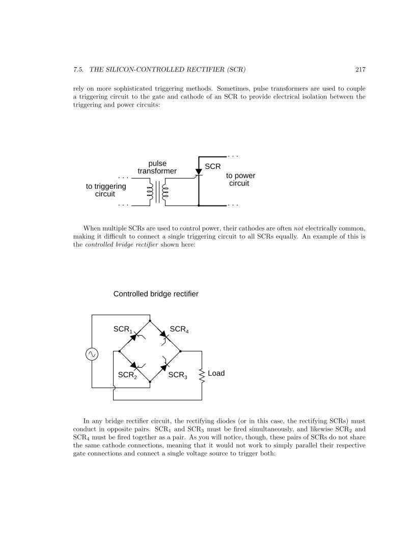
7.5. THE SILICON-CONTROLLED RECTIFIER (SCR) 217
rely on more sophisticated triggering methods. Sometimes, pulse transformers are used to couplea triggering circuit to the gate and cathode of an SCR to provide electrical isolation between thetriggering and power circuits:
. . .
. . .
to triggeringcircuit
. . .
. . .
to powercircuit
pulsetransformer
SCR
When multiple SCRs are used to control power, their cathodes are often not electrically common,making it difficult to connect a single triggering circuit to all SCRs equally. An example of this isthe controlled bridge rectifier shown here:
Load
Controlled bridge rectifier
SCR1
SCR2 SCR3
SCR4
In any bridge rectifier circuit, the rectifying diodes (or in this case, the rectifying SCRs) mustconduct in opposite pairs. SCR1 and SCR3 must be fired simultaneously, and likewise SCR2 andSCR4 must be fired together as a pair. As you will notice, though, these pairs of SCRs do not sharethe same cathode connections, meaning that it would not work to simply parallel their respectivegate connections and connect a single voltage source to trigger both:

218 CHAPTER 7. THYRISTORS
Load
SCR1
SCR2 SCR3
SCR4
This strategy will not work for triggering SCR2 and SCR4together as a pair!
triggeringvoltage
(pulse voltagesource)
Although the triggering voltage source shown will trigger SCR4, it will not trigger SCR2 properlybecause the two thyristors do not share a common cathode connection to reference that triggeringvoltage. Pulse transformers connecting the two thyristor gates to a common triggering voltage sourcewill work, however:
Load
SCR1
SCR2 SCR3
SCR4 pulsevoltagesource
Bear in mind that this circuit only shows the gate connections for two out of the four SCRs.Pulse transformers and triggering sources for SCR1 and SCR3, as well as the details of the pulsesources themselves, have been omitted for the sake of simplicity.
Controlled bridge rectifiers are not limited to single-phase designs. In most industrial controlsystems, AC power is available in three-phase form for maximum efficiency, and solid-state controlcircuits are built to take advantage of that. A three-phase controlled rectifier circuit built withSCRs, without pulse transformers or triggering circuitry shown, would look like this:
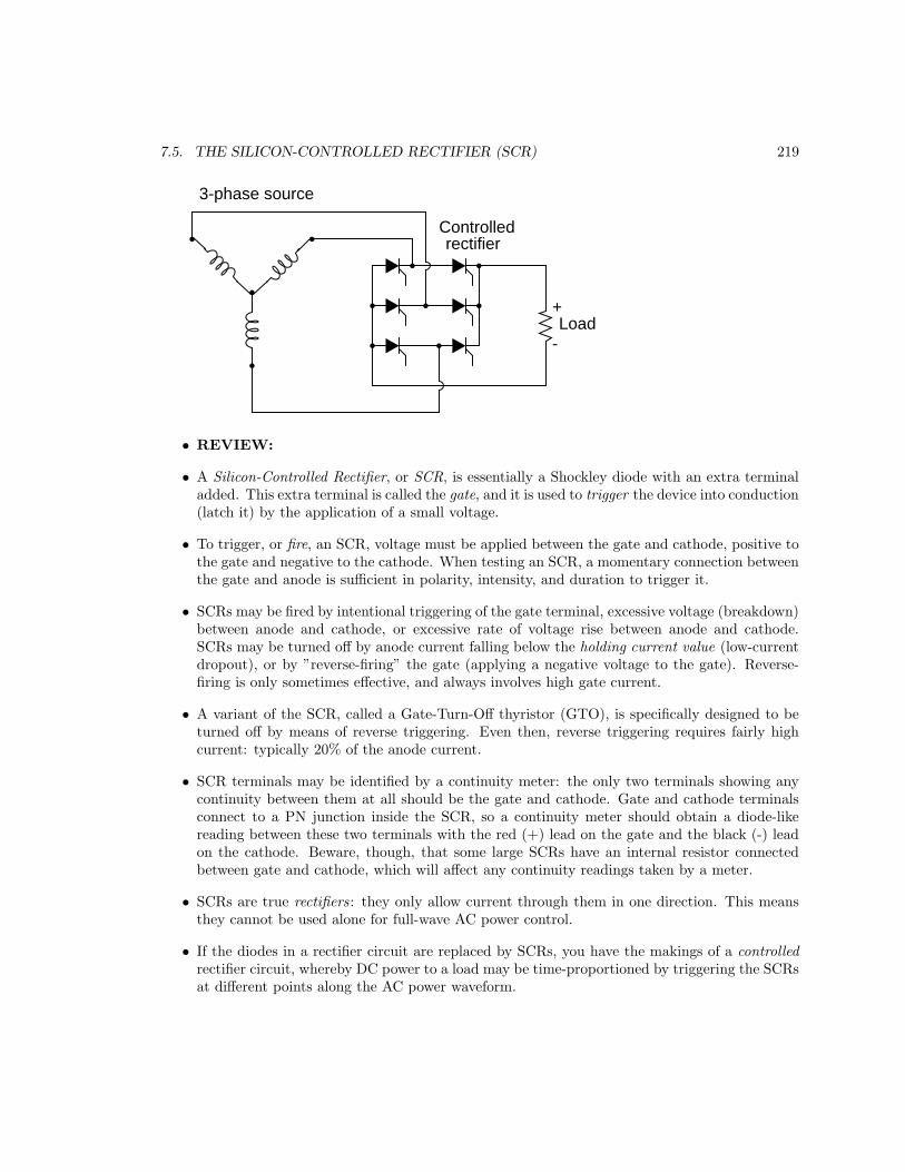
7.5. THE SILICON-CONTROLLED RECTIFIER (SCR) 219
Load
3-phase source
Controlledrectifier
+
-
• REVIEW:
• A Silicon-Controlled Rectifier, or SCR, is essentially a Shockley diode with an extra terminaladded. This extra terminal is called the gate, and it is used to trigger the device into conduction(latch it) by the application of a small voltage.
• To trigger, or fire, an SCR, voltage must be applied between the gate and cathode, positive tothe gate and negative to the cathode. When testing an SCR, a momentary connection betweenthe gate and anode is sufficient in polarity, intensity, and duration to trigger it.
• SCRs may be fired by intentional triggering of the gate terminal, excessive voltage (breakdown)between anode and cathode, or excessive rate of voltage rise between anode and cathode.SCRs may be turned off by anode current falling below the holding current value (low-currentdropout), or by ”reverse-firing” the gate (applying a negative voltage to the gate). Reverse-firing is only sometimes effective, and always involves high gate current.
• A variant of the SCR, called a Gate-Turn-Off thyristor (GTO), is specifically designed to beturned off by means of reverse triggering. Even then, reverse triggering requires fairly highcurrent: typically 20% of the anode current.
• SCR terminals may be identified by a continuity meter: the only two terminals showing anycontinuity between them at all should be the gate and cathode. Gate and cathode terminalsconnect to a PN junction inside the SCR, so a continuity meter should obtain a diode-likereading between these two terminals with the red (+) lead on the gate and the black (-) leadon the cathode. Beware, though, that some large SCRs have an internal resistor connectedbetween gate and cathode, which will affect any continuity readings taken by a meter.
• SCRs are true rectifiers: they only allow current through them in one direction. This meansthey cannot be used alone for full-wave AC power control.
• If the diodes in a rectifier circuit are replaced by SCRs, you have the makings of a controlledrectifier circuit, whereby DC power to a load may be time-proportioned by triggering the SCRsat different points along the AC power waveform.

220 CHAPTER 7. THYRISTORS
7.6 The TRIAC
SCRs are unidirectional (one-way) current devices, making them useful for controlling DC only.If two SCRs are joined in back-to-back parallel fashion just like two Shockley diodes were joinedtogether to form a DIAC, we have a new device known as the TRIAC :
TRIAC equivalent circuit TRIAC schematic symbol
Gate
Main Terminal 1
Main Terminal 2(MT2)
(MT1)
Main Terminal 2(MT2)
Main Terminal 1(MT1)
Gate
Because individual SCRs are more flexible to use in advanced control systems, they are morecommonly seen in circuits like motor drives, while TRIACs are usually seen in simple, low-powerapplications like household dimmer switches. A simple lamp dimmer circuit is shown here, completewith the phase-shifting resistor-capacitor network necessary for after-peak firing.
ACsource
Lamp
TRIACs are notorious for not firing symmetrically. This means they usually won’t trigger atthe exact same gate voltage level for one polarity as for the other. Generally speaking, this isundesirable, because unsymmetrical firing results in a current waveform with a greater variety ofharmonic frequencies. Waveforms that are symmetrical above and below their average centerlines arecomprised of only odd-numbered harmonics. Unsymmetrical waveforms, on the other hand, containeven-numbered harmonics (which may or may not be accompanied by odd-numbered harmonics aswell).
In the interest of reducing total harmonic content in power systems, the fewer and less diverse theharmonics, the better – one more reason why individual SCRs are favored over TRIACs for complex,high-power control circuits. One way to make the TRIAC’s current waveform more symmetrical isto use a device external to the TRIAC to time the triggering pulse. A DIAC placed in series withthe gate does a fair job of this:

7.6. THE TRIAC 221
ACsource
Lamp
DIAC breakover voltages tend to be much more symmetrical (the same in one polarity as theother) than TRIAC triggering voltage thresholds. Since the DIAC prevents any gate current untilthe triggering voltage has reached a certain, repeatable level in either direction, the firing point ofthe TRIAC from one half-cycle to the next tends to be more consistent, and the waveform moresymmetrical above and below its centerline.
Practically all the characteristics and ratings of SCRs apply equally to TRIACs, except thatTRIACs of course are bidirectional (can handle current in both directions). Not much more needsto be said about this device except for an important caveat concerning its terminal designations.
From the equivalent circuit diagram shown earlier, one might think that main terminals 1 and 2were interchangeable. They are not! Although it is helpful to imagine the TRIAC as being composedof two SCRs joined together, it in fact is constructed from a single piece of semiconducting material,appropriately doped and layered. The actual operating characteristics may differ slightly from thatof the equivalent model.
This is made most evident by contrasting two simple circuit designs, one that works and one thatdoesn’t. The following two circuits are a variation of the lamp dimmer circuit shown earlier, thephase-shifting capacitor and DIAC removed for simplicity’s sake. Although the resulting circuit lacksthe fine control ability of the more complex version (with capacitor and DIAC), it does function:
ACsource
Lamp
Suppose we were to swap the two main terminals of the TRIAC around. According to theequivalent circuit diagram shown earlier in this section, the swap should make no difference. Thecircuit ought to work:
ACsource
Lamp
This circuit will not work!

222 CHAPTER 7. THYRISTORS
However, if this circuit is built, it will be found that it does not work! The load will receive nopower, the TRIAC refusing to fire at all, no matter how low or high a resistance value the controlresistor is set to. The key to successfully triggering a TRIAC is to make sure the gate receives itstriggering current from the main terminal 2 side of the circuit (the main terminal on the oppositeside of the TRIAC symbol from the gate terminal). Identification of the MT1 and MT2 terminalsmust be done via the TRIAC’s part number with reference to a data sheet or book.
• REVIEW:
• A TRIAC acts much like two SCRs connected back-to-back for bidirectional (AC) operation.
• TRIAC controls are more often seen in simple, low-power circuits than complex, high-powercircuits. In large power control circuits, multiple SCRs tend to be favored.
• When used to control AC power to a load, TRIACs are often accompanied by DIACs connectedin series with their gate terminals. The DIAC helps the TRIAC fire more symmetrically (moreconsistently from one polarity to another).
• Main terminals 1 and 2 on a TRIAC are not interchangeable.
• To successfully trigger a TRIAC, gate current must come from the main terminal 2 (MT2)side of the circuit!
7.7 Optothyristors
Like bipolar transistors, SCRs and TRIACs are also manufactured as light-sensitive devices, theaction of impinging light replacing the function of triggering voltage.Optically-controlled SCRs are often known by the acronym LASCR, or Light Activated SCR.
Its symbol, not surprisingly, looks like this:
Light Activated SCR
LASCR
Optically-controlled TRIACs don’t receive the honor of having their own acronym, but insteadare humbly known as opto-TRIACs. Their schematic symbol looks like this:
Opto-TRIAC
Optothyristors (a general term for either the LASCR or the opto-TRIAC) are commonly foundinside sealed ”optoisolator” modules.

7.8. THE UNIJUNCTION TRANSISTOR (UJT) – PENDING 223
7.8 The Unijunction Transistor (UJT) – PENDING
Programmable Unijunction Transistors (PUTs).
• REVIEW:
•
•
•
7.9 The Silicon-Controlled Switch (SCS)
If we take the equivalent circuit for an SCR and add another external terminal, connected to thebase of the top transistor and the collector of the bottom transistor, we have a device known as asilicon-controlled-switch, or SCS :
P
P
N
N
Anode
N
P
Cathode Cathode
Anode
Physical diagram Equivalent schematic Schematic symbol
Gate
Cathode
Anode
The Silicon-Controlled Switch (SCS)
Cathode GateAnode
CathodeGate
AnodeGate
CathodeGate
AnodeGate
This extra terminal allows more control to be exerted over the device, particularly in the modeof forced commutation, where an external signal forces it to turn off while the main current throughthe device has not yet fallen below the holding current value. Consider the following circuit:

224 CHAPTER 7. THYRISTORS
on
off
Motor
DC motor start/stopcircuit using an SCS
R1
R2
on
off
Motor
R1 R2
Equivalent schematic with two transistors
SCS
SCS
When the ”on” pushbutton switch is actuated, there is a voltage applied between the cathodegate and the cathode, forward-biasing the lower transistor’s base-emitter junction, and turning iton. The top transistor of the SCS is ready to conduct, having been supplied with a current pathfrom its emitter terminal (the SCS’s anode terminal) through resistor R2 to the positive side of thepower supply. As in the case of the SCR, both transistors turn on and maintain each other in the”on” mode. When the lower transistor turns on, it conducts the motor’s load current, and the motorstarts and runs.
The motor may be stopped by interrupting the power supply, as with an SCR, and this is callednatural commutation. However, the SCS provides us with another means of turning off: forcedcommutation by shorting the anode terminal to the cathode. If this is done (by actuating the ”off”pushbutton switch), the upper transistor within the SCS will lose its emitter current, thus haltingcurrent through the base of the lower transistor. When the lower transistor turns off, it breaks thecircuit for base current through the top transistor (securing its ”off” state), and the motor (makingit stop). The SCS will remain in the off condition until such time that the ”on” pushbutton switchis re-actuated.
• REVIEW:
• A silicon-controlled switch, or SCS, is essentially an SCR with an extra gate terminal.
• Typically, the load current through an SCS is carried by the anode gate and cathode terminals,with the cathode gate and anode terminals sufficing as control leads.
• An SCS is turned on by applying a positive voltage between the cathode gate and cathodeterminals. It may be turned off (forced commutation) by applying a negative voltage betweenthe anode and cathode terminals, or simply by shorting those two terminals together. Theanode terminal must be kept positive with respect to the cathode in order for the SCS tolatch.

7.10. FIELD-EFFECT-CONTROLLED THYRISTORS 225
7.10 Field-effect-controlled thyristors
Two relatively recent technologies designed to reduce the ”driving” (gate trigger current) require-ments of classic thyristor devices are the MOS-gated thyristor and the MOS Controlled Thyristor,or MCT.
The MOS-gated thyristor uses a MOSFET to initiate conduction through the upper (PNP)transistor of a normal thyristor structure, thus triggering the device. Since a MOSFET requiresnegligible current to ”drive” (cause it to saturate), this makes the thyristor as a whole very easy totrigger:
Cathode
Anode
Gate
MOS-gated thyristorequivalent circuit
Given the fact that ordinary SCRs are quite easy to ”drive” as it is, the practical advantage ofusing an even more sensitive device (a MOSFET) to initiate triggering is debatable. Also, placinga MOSFET at the gate input of the thyristor now makes it impossible to turn it off by a reverse-triggering signal. Only low-current dropout can make this device stop conducting after it has beenlatched.
A device of arguably greater value would be a fully-controllable thyristor, whereby a small gatesignal could both trigger the thyristor and force it to turn off. Such a device does exist, and it iscalled the MOS Controlled Thyristor, or MCT. It uses a pair of MOSFETs connected to a commongate terminal, one to trigger the thyristor and the other to ”untrigger” it:
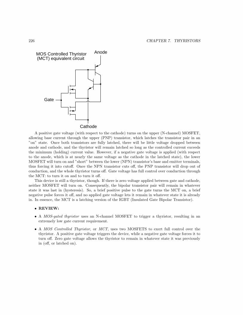
226 CHAPTER 7. THYRISTORS
Cathode
Anode
Gate
MOS Controlled Thyristor(MCT) equivalent circuit
A positive gate voltage (with respect to the cathode) turns on the upper (N-channel) MOSFET,allowing base current through the upper (PNP) transistor, which latches the transistor pair in an”on” state. Once both transistors are fully latched, there will be little voltage dropped betweenanode and cathode, and the thyristor will remain latched so long as the controlled current exceedsthe minimum (holding) current value. However, if a negative gate voltage is applied (with respectto the anode, which is at nearly the same voltage as the cathode in the latched state), the lowerMOSFET will turn on and ”short” between the lower (NPN) transistor’s base and emitter terminals,thus forcing it into cutoff. Once the NPN transistor cuts off, the PNP transistor will drop out ofconduction, and the whole thyristor turns off. Gate voltage has full control over conduction throughthe MCT: to turn it on and to turn it off.This device is still a thyristor, though. If there is zero voltage applied between gate and cathode,
neither MOSFET will turn on. Consequently, the bipolar transistor pair will remain in whateverstate it was last in (hysteresis). So, a brief positive pulse to the gate turns the MCT on, a briefnegative pulse forces it off, and no applied gate voltage lets it remain in whatever state it is alreadyin. In essence, the MCT is a latching version of the IGBT (Insulated Gate Bipolar Transistor).
• REVIEW:
• A MOS-gated thyristor uses an N-channel MOSFET to trigger a thyristor, resulting in anextremely low gate current requirement.
• A MOS Controlled Thyristor, or MCT, uses two MOSFETS to exert full control over thethyristor. A positive gate voltage triggers the device, while a negative gate voltage forces it toturn off. Zero gate voltage allows the thyristor to remain in whatever state it was previouslyin (off, or latched on).
Chapter 8
OPERATIONAL AMPLIFIERS
Contents
8.1 Introduction . . . . . . . . . . . . . . . . . . . . . . . . . . . . . . . . . . 227
8.2 Single-ended and differential amplifiers . . . . . . . . . . . . . . . . . . 228
8.3 The ”operational” amplifier . . . . . . . . . . . . . . . . . . . . . . . . . 232
8.4 Negative feedback . . . . . . . . . . . . . . . . . . . . . . . . . . . . . . . 238
8.5 Divided feedback . . . . . . . . . . . . . . . . . . . . . . . . . . . . . . . . 241
8.6 An analogy for divided feedback . . . . . . . . . . . . . . . . . . . . . . 244
8.7 Voltage-to-current signal conversion . . . . . . . . . . . . . . . . . . . . 249
8.8 Averager and summer circuits . . . . . . . . . . . . . . . . . . . . . . . . 250
8.9 Building a differential amplifier . . . . . . . . . . . . . . . . . . . . . . . 253
8.10 The instrumentation amplifier . . . . . . . . . . . . . . . . . . . . . . . . 255
8.11 Differentiator and integrator circuits . . . . . . . . . . . . . . . . . . . . 256
8.12 Positive feedback . . . . . . . . . . . . . . . . . . . . . . . . . . . . . . . . 259
8.13 Practical considerations: common-mode gain . . . . . . . . . . . . . . . 263
8.14 Practical considerations: offset voltage . . . . . . . . . . . . . . . . . . 267
8.15 Practical considerations: bias current . . . . . . . . . . . . . . . . . . . 269
8.16 Practical considerations: drift . . . . . . . . . . . . . . . . . . . . . . . . 274
8.17 Practical considerations: frequency response . . . . . . . . . . . . . . . 275
8.18 Operational amplifier models . . . . . . . . . . . . . . . . . . . . . . . . 276
8.19 Data . . . . . . . . . . . . . . . . . . . . . . . . . . . . . . . . . . . . . . . 281
8.1 Introduction
The operational amplifier is arguably the most useful single device in analog electronic circuitry.With only a handful of external components, it can be made to perform a wide variety of analogsignal processing tasks. It is also quite affordable, most general-purpose amplifiers selling for undera dollar apiece. Modern designs have been engineered with durability in mind as well: several ”op-amps” are manufactured that can sustain direct short-circuits on their outputs without damage.
227

228 CHAPTER 8. OPERATIONAL AMPLIFIERS
One key to the usefulness of these little circuits is in the engineering principle of feedback,particularly negative feedback, which constitutes the foundation of almost all automatic controlprocesses. The principles presented here in operational amplifier circuits, therefore, extend wellbeyond the immediate scope of electronics. It is well worth the electronics student’s time to learnthese principles and learn them well.
8.2 Single-ended and differential amplifiers
For ease of drawing complex circuit diagrams, electronic amplifiers are often symbolized by a simpletriangle shape, where the internal components are not individually represented. This symbology isvery handy for cases where an amplifier’s construction is irrelevant to the greater function of theoverall circuit, and it is worthy of familiarization:
Input Output
+Vsupply
-Vsupply
General amplifier circuit symbol
The +V and -V connections denote the positive and negative sides of the DC power supply,respectively. The input and output voltage connections are shown as single conductors, because it isassumed that all signal voltages are referenced to a common connection in the circuit called ground.Often (but not always!), one pole of the DC power supply, either positive or negative, is that groundreference point. A practical amplifier circuit (showing the input voltage source, load resistance, andpower supply) might look like this:
Rload
Vinput
Input Output
+V
-V
30 V+
-
Without having to analyze the actual transistor design of the amplifier, you can readily discernthe whole circuit’s function: to take an input signal (Vin), amplify it, and drive a load resistance(Rload). To complete the above schematic, it would be good to specify the gains of that amplifier(AV , AI , AP ) and the Q (bias) point for any needed mathematical analysis.
If it is necessary for an amplifier to be able to output true AC voltage (reversing polarity) tothe load, a split DC power supply may be used, whereby the ground point is electrically ”centered”
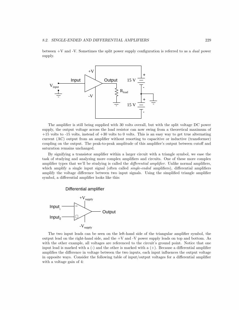
8.2. SINGLE-ENDED AND DIFFERENTIAL AMPLIFIERS 229
between +V and -V. Sometimes the split power supply configuration is referred to as a dual powersupply.
Rload
Vinput
Input Output
+V
-V
+
-
+
-
15 V
15 V
The amplifier is still being supplied with 30 volts overall, but with the split voltage DC powersupply, the output voltage across the load resistor can now swing from a theoretical maximum of+15 volts to -15 volts, instead of +30 volts to 0 volts. This is an easy way to get true alternatingcurrent (AC) output from an amplifier without resorting to capacitive or inductive (transformer)coupling on the output. The peak-to-peak amplitude of this amplifier’s output between cutoff andsaturation remains unchanged.
By signifying a transistor amplifier within a larger circuit with a triangle symbol, we ease thetask of studying and analyzing more complex amplifiers and circuits. One of these more complexamplifier types that we’ll be studying is called the differential amplifier. Unlike normal amplifiers,which amplify a single input signal (often called single-ended amplifiers), differential amplifiersamplify the voltage difference between two input signals. Using the simplified triangle amplifiersymbol, a differential amplifier looks like this:
−
+
Input1
Input2
+Vsupply
-Vsupply
Output
Differential amplifier
The two input leads can be seen on the left-hand side of the triangular amplifier symbol, theoutput lead on the right-hand side, and the +V and -V power supply leads on top and bottom. Aswith the other example, all voltages are referenced to the circuit’s ground point. Notice that oneinput lead is marked with a (-) and the other is marked with a (+). Because a differential amplifieramplifies the difference in voltage between the two inputs, each input influences the output voltagein opposite ways. Consider the following table of input/output voltages for a differential amplifierwith a voltage gain of 4:

230 CHAPTER 8. OPERATIONAL AMPLIFIERS
Output
(-) Input1
(+) Input2
0
0
0
0 0 0 1 2.5 7
0 0 01 2.5 7
4 10 28 -4 -10 -28
3
3
-3
3
0 24
-2
-7
-20
Voltage output equation: Vout = AV(Input2 - Input1)
orVout = AV(Input(+) - Input(-))
An increasingly positive voltage on the (+) input tends to drive the output voltage more positive,and an increasingly positive voltage on the (-) input tends to drive the output voltage more negative.Likewise, an increasingly negative voltage on the (+) input tends to drive the output negative aswell, and an increasingly negative voltage on the (-) input does just the opposite. Because of thisrelationship between inputs and polarities, the (-) input is commonly referred to as the invertinginput and the (+) as the noninverting input.
It may be helpful to think of a differential amplifier as a variable voltage source controlled by asensitive voltmeter, as such:
G
-
+
+V
-V
-
+
Bear in mind that the above illustration is only a model to aid in understanding the behavior of adifferential amplifier. It is not a realistic schematic of its actual design. The ”G” symbol representsa galvanometer, a sensitive voltmeter movement. The potentiometer connected between +V and -Vprovides a variable voltage at the output pin (with reference to one side of the DC power supply),that variable voltage set by the reading of the galvanometer. It must be understood that any loadpowered by the output of a differential amplifier gets its current from the DC power source (battery),not the input signal. The input signal (to the galvanometer) merely controls the output.
This concept may at first be confusing to students new to amplifiers. With all these polaritiesand polarity markings (- and +) around, it’s easy to get confused and not know what the output ofa differential amplifier will be. To address this potential confusion, here’s a simple rule to remember:

8.2. SINGLE-ENDED AND DIFFERENTIAL AMPLIFIERS 231
−
+Differential
input voltage
-
+
+
-Outputvoltage
Differentialinput voltage
-
+ −
++
-voltageOutput
When the polarity of the differential voltage matches the markings for inverting and noninvertinginputs, the output will be positive. When the polarity of the differential voltage clashes with theinput markings, the output will be negative. This bears some similarity to the mathematical signdisplayed by digital voltmeters based on input voltage polarity. The red test lead of the voltmeter(often called the ”positive” lead because of the color red’s popular association with the positive sideof a power supply in electronic wiring) is more positive than the black, the meter will display apositive voltage figure, and vice versa:
Differentialinput voltage
-
+
Differentialinput voltage
-
+
6 V
6 V
-
+
-
+red
blk
blk
red
Digital Voltmeter
Digital Voltmeter
+ 6.00 V
- 6.00 V
Just as a voltmeter will only display the voltage between its two test leads, an ideal differentialamplifier only amplifies the potential difference between its two input connections, not the voltagebetween any one of those connections and ground. The output polarity of a differential amplifier, justlike the signed indication of a digital voltmeter, depends on the relative polarities of the differentialvoltage between the two input connections.
If the input voltages to this amplifier represented mathematical quantities (as is the case withinanalog computer circuitry), or physical process measurements (as is the case within analog electronicinstrumentation circuitry), you can see how a device such as a differential amplifier could be veryuseful. We could use it to compare two quantities to see which is greater (by the polarity of theoutput voltage), or perhaps we could compare the difference between two quantities (such as thelevel of liquid in two tanks) and flag an alarm (based on the absolute value of the amplifier output) ifthe difference became too great. In basic automatic control circuitry, the quantity being controlled(called the process variable) is compared with a target value (called the setpoint), and decisionsare made as to how to act based on the discrepancy between these two values. The first step inelectronically controlling such a scheme is to amplify the difference between the process variable and

232 CHAPTER 8. OPERATIONAL AMPLIFIERS
the setpoint with a differential amplifier. In simple controller designs, the output of this differentialamplifier can be directly utilized to drive the final control element (such as a valve) and keep theprocess reasonably close to setpoint.
• REVIEW:
• A ”shorthand” symbol for an electronic amplifier is a triangle, the wide end signifying theinput side and the narrow end signifying the output. Power supply lines are often omitted inthe drawing for simplicity.
• To facilitate true AC output from an amplifier, we can use what is called a split or dual powersupply, with two DC voltage sources connected in series with the middle point grounded, givinga positive voltage to ground (+V) and a negative voltage to ground (-V). Split power supplieslike this are frequently used in differential amplifier circuits.
• Most amplifiers have one input and one output. Differential amplifiers have two inputs andone output, the output signal being proportional to the difference in signals between the twoinputs.
• The voltage output of a differential amplifier is determined by the following equation: Vout =AV (Vnoninv - Vinv)
8.3 The ”operational” amplifier
Long before the advent of digital electronic technology, computers were built to electronically per-form calculations by employing voltages and currents to represent numerical quantities. This wasespecially useful for the simulation of physical processes. A variable voltage, for instance, might rep-resent velocity or force in a physical system. Through the use of resistive voltage dividers and voltageamplifiers, the mathematical operations of division and multiplication could be easily performed onthese signals.The reactive properties of capacitors and inductors lend themselves well to the simulation of
variables related by calculus functions. Remember how the current through a capacitor was afunction of the voltage’s rate of change, and how that rate of change was designated in calculus asthe derivative? Well, if voltage across a capacitor were made to represent the velocity of an object,the current through the capacitor would represent the force required to accelerate or decelerate thatobject, the capacitor’s capacitance representing the object’s mass:
iC = C dvdt
F = m dvdt
Where, Where,
iC =
C =
dvdt
=
Instantaneous current through capacitorCapacitance in farads
Rate of change of voltage over time
F =
m =
dvdt
=
Force applied to object
Mass of object
Rate of change of velocity over time

8.3. THE ”OPERATIONAL” AMPLIFIER 233
This analog electronic computation of the calculus derivative function is technically known asdifferentiation, and it is a natural function of a capacitor’s current in relation to the voltage appliedacross it. Note that this circuit requires no ”programming” to perform this relatively advancedmathematical function as a digital computer would.
Electronic circuits are very easy and inexpensive to create compared to complex physical systems,so this kind of analog electronic simulation was widely used in the research and development ofmechanical systems. For realistic simulation, though, amplifier circuits of high accuracy and easyconfigurability were needed in these early computers.
It was found in the course of analog computer design that differential amplifiers with extremelyhigh voltage gains met these requirements of accuracy and configurability better than single-endedamplifiers with custom-designed gains. Using simple components connected to the inputs and outputof the high-gain differential amplifier, virtually any gain and any function could be obtained from thecircuit, overall, without adjusting or modifying the internal circuitry of the amplifier itself. Thesehigh-gain differential amplifiers came to be known as operational amplifiers, or op-amps, because oftheir application in analog computers’ mathematical operations.
Modern op-amps, like the popular model 741, are high-performance, inexpensive integrated cir-cuits. Their input impedances are quite high, the inputs drawing currents in the range of halfa microamp (maximum) for the 741, and far less for op-amps utilizing field-effect input transis-tors. Output impedance is typically quite low, about 75 Ω for the model 741, and many modelshave built-in output short circuit protection, meaning that their outputs can be directly shortedto ground without causing harm to the internal circuitry. With direct coupling between op-amps’internal transistor stages, they can amplify DC signals just as well as AC (up to certain maximumvoltage-risetime limits). It would cost far more in money and time to design a comparable discrete-transistor amplifier circuit to match that kind of performance, unless high power capability wasrequired. For these reasons, op-amps have all but obsoleted discrete-transistor signal amplifiers inmany applications.
The following diagram shows the pin connections for single op-amps (741 included) when housedin an 8-pin DIP (Dual Inline Package) integrated circuit:

234 CHAPTER 8. OPERATIONAL AMPLIFIERS
Typical 8-pin "DIP" op-ampintegrated circuit
8 7 6
1 2 3 4
5
− ++V
-V
OutputNo
connectionOffset
null
Offsetnull
Some models of op-amp come two to a package, including the popular models TL082 and 1458.These are called ”dual” units, and are typically housed in an 8-pin DIP package as well, with thefollowing pin connections:
8 7 6
1 2 3 4
5
Dual op-amp in 8-pin DIP
+V
-V
−
+
−
+
Operational amplifiers are also available four to a package, usually in 14-pin DIP arrangements.Unfortunately, pin assignments aren’t as standard for these ”quad” op-amps as they are for the”dual” or single units. Consult the manufacturer datasheet(s) for details.Practical operational amplifier voltage gains are in the range of 200,000 or more, which makes

8.3. THE ”OPERATIONAL” AMPLIFIER 235
them almost useless as an analog differential amplifier by themselves. For an op-amp with a voltagegain (AV ) of 200,000 and a maximum output voltage swing of +15V/-15V, all it would take is adifferential input voltage of 75 µV (microvolts) to drive it to saturation or cutoff! Before we takea look at how external components are used to bring the gain down to a reasonable level, let’sinvestigate applications for the ”bare” op-amp by itself.
One application is called the comparator. For all practical purposes, we can say that the outputof an op-amp will be saturated fully positive if the (+) input is more positive than the (-) input,and saturated fully negative if the (+) input is less positive than the (-) input. In other words,an op-amp’s extremely high voltage gain makes it useful as a device to compare two voltages andchange output voltage states when one input exceeds the other in magnitude.
−
+
+V
-V
LEDVin
In the above circuit, we have an op-amp connected as a comparator, comparing the input voltagewith a reference voltage set by the potentiometer (R1). If Vin drops below the voltage set by R1,the op-amp’s output will saturate to +V, thereby lighting up the LED. Otherwise, if Vin is abovethe reference voltage, the LED will remain off. If Vin is a voltage signal produced by a measuringinstrument, this comparator circuit could function as a ”low” alarm, with the trip-point set by R1.Instead of an LED, the op-amp output could drive a relay, a transistor, an SCR, or any other devicecapable of switching power to a load such as a solenoid valve, to take action in the event of a lowalarm.
Another application for the comparator circuit shown is a square-wave converter. Suppose thatthe input voltage applied to the inverting (-) input was an AC sine wave rather than a stable DCvoltage. In that case, the output voltage would transition between opposing states of saturationwhenever the input voltage was equal to the reference voltage produced by the potentiometer. Theresult would be a square wave:

236 CHAPTER 8. OPERATIONAL AMPLIFIERS
−
+
+V
-V
VoutVin
Vin Vout
Adjustments to the potentiometer setting would change the reference voltage applied to thenoninverting (+) input, which would change the points at which the sine wave would cross, changingthe on/off times, or duty cycle of the square wave:
−
+
+V
-V
VoutVin
Vin Vout
It should be evident that the AC input voltage would not have to be a sine wave in particularfor this circuit to perform the same function. The input voltage could be a triangle wave, sawtoothwave, or any other sort of wave that ramped smoothly from positive to negative to positive again.This sort of comparator circuit is very useful for creating square waves of varying duty cycle. Thistechnique is sometimes referred to as pulse-width modulation, or PWM (varying, or modulating awaveform according to a controlling signal, in this case the signal produced by the potentiometer).
Another comparator application is that of the bargraph driver. If we had several op-ampsconnected as comparators, each with its own reference voltage connected to the inverting input, but

8.3. THE ”OPERATIONAL” AMPLIFIER 237
each one monitoring the same voltage signal on their noninverting inputs, we could build a bargraph-style meter such as what is commonly seen on the face of stereo tuners and graphic equalizers. As thesignal voltage (representing radio signal strength or audio sound level) increased, each comparatorwould ”turn on” in sequence and send power to its respective LED. With each comparator switching”on” at a different level of audio sound, the number of LED’s illuminated would indicate how strongthe signal was.
−
+
−
+
−
+
−
+
+V
-V
Vin
-V
LED1
LED2
LED3
LED4
Simple bargraph driver circuit
In the circuit shown above, LED1 would be the first to light up as the input voltage increased ina positive direction. As the input voltage continued to increase, the other LED’s would illuminatein succession, until all were lit.This very same technology is used in some analog-to-digital signal converters, namely the flash
converter, to translate an analog signal quantity into a series of on/off voltages representing a digitalnumber.
• REVIEW:
• A triangle shape is the generic symbol for an amplifier circuit, the wide end signifying theinput and the narrow end signifying the output.
• Unless otherwise specified, all voltages in amplifier circuits are referenced to a common groundpoint, usually connected to one terminal of the power supply. This way, we can speak ofa certain amount of voltage being ”on” a single wire, while realizing that voltage is alwaysmeasured between two points.

238 CHAPTER 8. OPERATIONAL AMPLIFIERS
• A differential amplifier is one amplifying the voltage difference between two signal inputs. Insuch a circuit, one input tends to drive the output voltage to the same polarity of the inputsignal, while the other input does just the opposite. Consequently, the first input is called thenoninverting (+) input and the second is called the inverting (-) input.
• An operational amplifier (or op-amp for short) is a differential amplifier with an extremely highvoltage gain (AV = 200,000 or more). Its name hails from its original use in analog computercircuitry (performing mathematical operations).
• Op-amps typically have very high input impedances and fairly low output impedances.
• Sometimes op-amps are used as signal comparators, operating in full cutoff or saturation modedepending on which input (inverting or noninverting) has the greatest voltage. Comparatorsare useful in detecting ”greater-than” signal conditions (comparing one to the other).
• One comparator application is called the pulse-width modulator, and is made by comparing asine-wave AC signal against a DC reference voltage. As the DC reference voltage is adjusted,the square-wave output of the comparator changes its duty cycle (positive versus negativetimes). Thus, the DC reference voltage controls, or modulates the pulse width of the outputvoltage.
8.4 Negative feedback
If we connect the output of an op-amp to its inverting input and apply a voltage signal to thenoninverting input, we find that the output voltage of the op-amp closely follows that input voltage(I’ve neglected to draw in the power supply, +V/-V wires, and ground symbol for simplicity):
−
+Vin
Vout
As Vin increases, Vout will increase in accordance with the differential gain. However, as Vout
increases, that output voltage is fed back to the inverting input, thereby acting to decrease thevoltage differential between inputs, which acts to bring the output down. What will happen for anygiven voltage input is that the op-amp will output a voltage very nearly equal to Vin, but just lowenough so that there’s enough voltage difference left between Vin and the (-) input to be amplifiedto generate the output voltage.The circuit will quickly reach a point of stability (known as equilibrium in physics), where the
output voltage is just the right amount to maintain the right amount of differential, which in turnproduces the right amount of output voltage. Taking the op-amp’s output voltage and couplingit to the inverting input is a technique known as negative feedback, and it is the key to having aself-stabilizing system (this is true not only of op-amps, but of any dynamic system in general). Thisstability gives the op-amp the capacity to work in its linear (active) mode, as opposed to merelybeing saturated fully ”on” or ”off” as it was when used as a comparator, with no feedback at all.Because the op-amp’s gain is so high, the voltage on the inverting input can be maintained almost
equal to Vin. Let’s say that our op-amp has a differential voltage gain of 200,000. If Vin equals
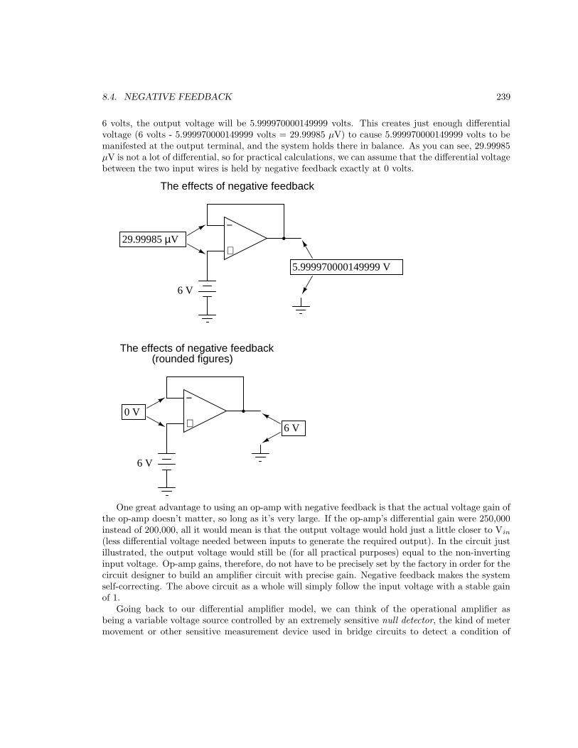
8.4. NEGATIVE FEEDBACK 239
6 volts, the output voltage will be 5.999970000149999 volts. This creates just enough differentialvoltage (6 volts - 5.999970000149999 volts = 29.99985 µV) to cause 5.999970000149999 volts to bemanifested at the output terminal, and the system holds there in balance. As you can see, 29.99985µV is not a lot of differential, so for practical calculations, we can assume that the differential voltagebetween the two input wires is held by negative feedback exactly at 0 volts.
−
+
6 V
5.999970000149999 V
29.99985 µV
The effects of negative feedback
−
+
6 V
The effects of negative feedback
0 V
6 V
(rounded figures)
One great advantage to using an op-amp with negative feedback is that the actual voltage gain ofthe op-amp doesn’t matter, so long as it’s very large. If the op-amp’s differential gain were 250,000instead of 200,000, all it would mean is that the output voltage would hold just a little closer to Vin
(less differential voltage needed between inputs to generate the required output). In the circuit justillustrated, the output voltage would still be (for all practical purposes) equal to the non-invertinginput voltage. Op-amp gains, therefore, do not have to be precisely set by the factory in order for thecircuit designer to build an amplifier circuit with precise gain. Negative feedback makes the systemself-correcting. The above circuit as a whole will simply follow the input voltage with a stable gainof 1.Going back to our differential amplifier model, we can think of the operational amplifier as
being a variable voltage source controlled by an extremely sensitive null detector, the kind of metermovement or other sensitive measurement device used in bridge circuits to detect a condition of

240 CHAPTER 8. OPERATIONAL AMPLIFIERS
balance (zero volts). The ”potentiometer” inside the op-amp creating the variable voltage will moveto whatever position it must to ”balance” the inverting and noninverting input voltages so that the”null detector” has zero voltage across it:
null
-
+
+V
-V
6 V
6 V
0 V
As the ”potentiometer” will move to provide an output voltage necessary to satisfy the ”nulldetector” at an ”indication” of zero volts, the output voltage becomes equal to the input voltage:in this case, 6 volts. If the input voltage changes at all, the ”potentiometer” inside the op-amp willchange position to hold the ”null detector” in balance (indicating zero volts), resulting in an outputvoltage approximately equal to the input voltage at all times.This will hold true within the range of voltages that the op-amp can output. With a power
supply of +15V/-15V, and an ideal amplifier that can swing its output voltage just as far, it willfaithfully ”follow” the input voltage between the limits of +15 volts and -15 volts. For this reason,the above circuit is known as a voltage follower. Like its one-transistor counterpart, the common-collector (”emitter-follower”) amplifier, it has a voltage gain of 1, a high input impedance, a lowoutput impedance, and a high current gain. Voltage followers are also known as voltage buffers,and are used to boost the current-sourcing ability of voltage signals too weak (too high of sourceimpedance) to directly drive a load. The op-amp model shown in the last illustration depicts howthe output voltage is essentially isolated from the input voltage, so that current on the output pinis not supplied by the input voltage source at all, but rather from the power supply powering theop-amp.It should be mentioned that many op-amps cannot swing their output voltages exactly to +V/-V
power supply rail voltages. The model 741 is one of those that cannot: when saturated, its outputvoltage peaks within about one volt of the +V power supply voltage and within about 2 volts ofthe -V power supply voltage. Therefore, with a split power supply of +15/-15 volts, a 741 op-amp’soutput may go as high as +14 volts or as low as -13 volts (approximately), but no further. This isdue to its bipolar transistor design. These two voltage limits are known as the positive saturationvoltage and negative saturation voltage, respectively. Other op-amps, such as the model 3130 withfield-effect transistors in the final output stage, have the ability to swing their output voltages withinmillivolts of either power supply rail voltage. Consequently, their positive and negative saturationvoltages are practically equal to the supply voltages.
• REVIEW:
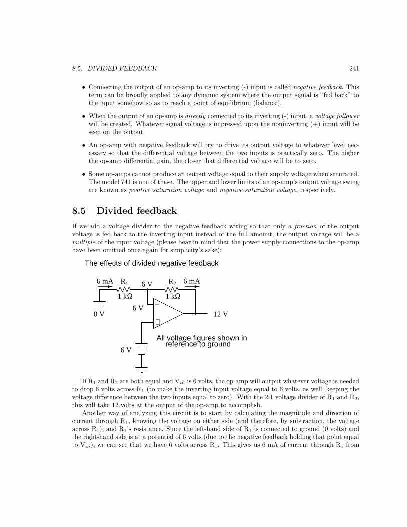
8.5. DIVIDED FEEDBACK 241
• Connecting the output of an op-amp to its inverting (-) input is called negative feedback. Thisterm can be broadly applied to any dynamic system where the output signal is ”fed back” tothe input somehow so as to reach a point of equilibrium (balance).
• When the output of an op-amp is directly connected to its inverting (-) input, a voltage followerwill be created. Whatever signal voltage is impressed upon the noninverting (+) input will beseen on the output.
• An op-amp with negative feedback will try to drive its output voltage to whatever level nec-essary so that the differential voltage between the two inputs is practically zero. The higherthe op-amp differential gain, the closer that differential voltage will be to zero.
• Some op-amps cannot produce an output voltage equal to their supply voltage when saturated.The model 741 is one of these. The upper and lower limits of an op-amp’s output voltage swingare known as positive saturation voltage and negative saturation voltage, respectively.
8.5 Divided feedback
If we add a voltage divider to the negative feedback wiring so that only a fraction of the outputvoltage is fed back to the inverting input instead of the full amount, the output voltage will be amultiple of the input voltage (please bear in mind that the power supply connections to the op-amphave been omitted once again for simplicity’s sake):
−
+
6 V
The effects of divided negative feedback
R1 R2
1 kΩ 1 kΩ
0 V
6 V
6 V12 V
All voltage figures shown inreference to ground
6 mA 6 mA
If R1 and R2 are both equal and Vin is 6 volts, the op-amp will output whatever voltage is neededto drop 6 volts across R1 (to make the inverting input voltage equal to 6 volts, as well, keeping thevoltage difference between the two inputs equal to zero). With the 2:1 voltage divider of R1 and R2,this will take 12 volts at the output of the op-amp to accomplish.Another way of analyzing this circuit is to start by calculating the magnitude and direction of
current through R1, knowing the voltage on either side (and therefore, by subtraction, the voltageacross R1), and R1’s resistance. Since the left-hand side of R1 is connected to ground (0 volts) andthe right-hand side is at a potential of 6 volts (due to the negative feedback holding that point equalto Vin), we can see that we have 6 volts across R1. This gives us 6 mA of current through R1 from

242 CHAPTER 8. OPERATIONAL AMPLIFIERS
left to right. Because we know that both inputs of the op-amp have extremely high impedance,we can safely assume they won’t add or subtract any current through the divider. In other words,we can treat R1 and R2 as being in series with each other: all of the electrons flowing through R1
must flow through R2. Knowing the current through R2 and the resistance of R2, we can calculatethe voltage across R2 (6 volts), and its polarity. Counting up voltages from ground (0 volts) to theright-hand side of R2, we arrive at 12 volts on the output.Upon examining the last illustration, one might wonder, ”where does that 1 mA of current go?”
The last illustration doesn’t show the entire current path, but in reality it comes from the negativeside of the DC power supply, through ground, through R1, through R2, through the output pin of theop-amp, and then back to the positive side of the DC power supply through the output transistor(s)of the op-amp. Using the null detector/potentiometer model of the op-amp, the current path lookslike this:
null
-
+
+V
-V
6 V
R1 R2
1 kΩ 1 kΩ
The 6 volt signal source does not have to supply any current for the circuit: it merely commandsthe op-amp to balance voltage between the inverting (-) and noninverting (+) input pins, and in sodoing produce an output voltage that is twice the input due to the dividing effect of the two 1 kΩresistors.We can change the voltage gain of this circuit, overall, just by adjusting the values of R1 and R2
(changing the ratio of output voltage that is fed back to the inverting input). Gain can be calculatedby the following formula:
AV = R2
R1+ 1
Note that the voltage gain for this design of amplifier circuit can never be less than 1. If we wereto lower R2 to a value of zero ohms, our circuit would be essentially identical to the voltage follower,with the output directly connected to the inverting input. Since the voltage follower has a gain of1, this sets the lower gain limit of the noninverting amplifier. However, the gain can be increasedfar beyond 1, by increasing R2 in proportion to R1.Also note that the polarity of the output matches that of the input, just as with a voltage
follower. A positive input voltage results in a positive output voltage, and vice versa (with respect

8.5. DIVIDED FEEDBACK 243
to ground). For this reason, this circuit is referred to as a noninverting amplifier.Just as with the voltage follower, we see that the differential gain of the op-amp is irrelevant, so
long as it’s very high. The voltages and currents in this circuit would hardly change at all if theop-amp’s voltage gain were 250,000 instead of 200,000. This stands as a stark contrast to single-transistor amplifier circuit designs, where the Beta of the individual transistor greatly influencedthe overall gains of the amplifier. With negative feedback, we have a self-correcting system thatamplifies voltage according to the ratios set by the feedback resistors, not the gains internal to theop-amp.Let’s see what happens if we retain negative feedback through a voltage divider, but apply the
input voltage at a different location:
−
+
6 V
R1 R2
1 kΩ 1 kΩ
0 VAll voltage figures shown in
reference to ground
0 V
-6 V
6 mA 6 mA
By grounding the noninverting input, the negative feedback from the output seeks to hold theinverting input’s voltage at 0 volts, as well. For this reason, the inverting input is referred to inthis circuit as a virtual ground, being held at ground potential (0 volts) by the feedback, yet notdirectly connected to (electrically common with) ground. The input voltage this time is applied tothe left-hand end of the voltage divider (R1 = R2 = 1 kΩ again), so the output voltage must swingto -6 volts in order to balance the middle at ground potential (0 volts). Using the same techniquesas with the noninverting amplifier, we can analyze this circuit’s operation by determining currentmagnitudes and directions, starting with R1, and continuing on to determining the output voltage.We can change the overall voltage gain of this circuit, overall, just by adjusting the values of R1
and R2 (changing the ratio of output voltage that is fed back to the inverting input). Gain can becalculated by the following formula:
AV = R2
R1
Note that this circuit’s voltage gain can be less than 1, depending solely on the ratio of R2 to R1.Also note that the output voltage is always the opposite polarity of the input voltage. A positiveinput voltage results in a negative output voltage, and vice versa (with respect to ground). For thisreason, this circuit is referred to as an inverting amplifier. Sometimes, the gain formula contains anegative sign (before the R2/R1 fraction) to reflect this reversal of polarities.These two amplifier circuits we’ve just investigated serve the purpose of multiplying or dividing
the magnitude of the input voltage signal. This is exactly how the mathematical operations ofmultiplication and division are typically handled in analog computer circuitry.
• REVIEW:
• By connecting the inverting (-) input of an op-amp directly to the output, we get negativefeedback, which gives us a voltage follower circuit. By connecting that negative feedback

244 CHAPTER 8. OPERATIONAL AMPLIFIERS
through a resistive voltage divider (feeding back a fraction of the output voltage to the invertinginput), the output voltage becomes a multiple of the input voltage.
• A negative-feedback op-amp circuit with the input signal going to the noninverting (+) inputis called a noninverting amplifier. The output voltage will be the same polarity as the input.Voltage gain is given by the following equation: AV = (R2/R1) + 1
• A negative-feedback op-amp circuit with the input signal going to the ”bottom” of the resistivevoltage divider, with the noninverting (+) input grounded, is called an inverting amplifier. Itsoutput voltage will be the opposite polarity of the input. Voltage gain is given by the followingequation: AV = R2/R1
8.6 An analogy for divided feedback
A helpful analogy for understanding divided feedback amplifier circuits is that of a mechanical lever,with relative motion of the lever’s ends representing change in input and output voltages, and thefulcrum (pivot point) representing the location of the ground point, real or virtual.Take for example the following noninverting op-amp circuit. We know from the prior section
that the voltage gain of a noninverting amplifier configuration can never be less than unity (1). Ifwe draw a lever diagram next to the amplifier schematic, with the distance between fulcrum andlever ends representative of resistor values, the motion of the lever will signify changes in voltage atthe input and output terminals of the amplifier:
−
+
R1 R2
1 kΩ 1 kΩ
0 V
Vin
Vin
Vout
R1 R2
Vout = 2(Vin)
Vout
Physicists call this type of lever, with the input force (effort) applied between the fulcrum andoutput (load), a third-class lever. It is characterized by an output displacement (motion) at leastas large than the input displacement – a ”gain” of at least 1 – and in the same direction. Applying

8.6. AN ANALOGY FOR DIVIDED FEEDBACK 245
a positive input voltage to this op-amp circuit is analogous to displacing the ”input” point on thelever upward:
−
+
R1 R2
1 kΩ 1 kΩ
0 V
Vin
Vin
Vout
Vout = 2(Vin)
Vout
+
-
+
-
Due to the displacement-amplifying characteristics of the lever, the ”output” point will movetwice as far as the ”input” point, and in the same direction. In the electronic circuit, the outputvoltage will equal twice the input, with the same polarity. Applying a negative input voltage isanalogous to moving the lever downward from its level ”zero” position, resulting in an amplifiedoutput displacement that is also negative:

246 CHAPTER 8. OPERATIONAL AMPLIFIERS
−
+
R1 R2
1 kΩ 1 kΩ
0 V
Vin
Vin
Vout
Vout = 2(Vin)
Vout
+
-
+
-
If we alter the resistor ratio R2/R1, we change the gain of the op-amp circuit. In lever terms,this means moving the input point in relation to the fulcrum and lever end, which similarly changesthe displacement ”gain” of the machine:
−
+
R1 R2
1 kΩ
0 V
Vin
Vin
Vout
R1 R2
Vout
3 kΩ
Vout = 4(Vin)
Now, any input signal will become amplified by a factor of four instead of by a factor of two:

8.6. AN ANALOGY FOR DIVIDED FEEDBACK 247
−
+
R1 R2
1 kΩ
0 V
Vin
Vin
Vout
Vout
3 kΩ
Vout = 4(Vin)
+
-
+
-
Inverting op-amp circuits may be modeled using the lever analogy as well. With the invertingconfiguration, the ground point of the feedback voltage divider is the op-amp’s inverting input withthe input to the left and the output to the right. This is mechanically equivalent to a first-classlever, where the input force (effort) is on the opposite side of the fulcrum from the output (load):
−
+
R1 R2
1 kΩ 1 kΩVin
Vout
Vin Vout
Vout = -(Vin)
R1 R2
With equal-value resistors (equal-lengths of lever on each side of the fulcrum), the output voltage(displacement) will be equal in magnitude to the input voltage (displacement), but of the oppositepolarity (direction). A positive input results in a negative output:

248 CHAPTER 8. OPERATIONAL AMPLIFIERS
−
+
R1 R2
1 kΩ 1 kΩVin
Vout
Vin
Vout
Vout = -(Vin)
+
--
+
Changing the resistor ratio R2/R1 changes the gain of the amplifier circuit, just as changing thefulcrum position on the lever changes its mechanical displacement ”gain.” Consider the followingexample, where R2 is made twice as large as R1:
−
+
R1 R2
1 kΩVin
Vout
Vin
Vout
+
--
+2 kΩ
Vout = -2(Vin)
With the inverting amplifier configuration, though, gains of less than 1 are possible, just as withfirst-class levers. Reversing R2 and R1 values is analogous to moving the fulcrum to its complemen-tary position on the lever: one-third of the way from the output end. There, the output displacementwill be one-half the input displacement:

8.7. VOLTAGE-TO-CURRENT SIGNAL CONVERSION 249
−
+
R1 R2
1 kΩVin
Vout
Vin
Vout
+
--
+2 kΩ
Vout = -0.5(Vin)
8.7 Voltage-to-current signal conversion
In instrumentation circuitry, DC signals are often used as analog representations of physical mea-surements such as temperature, pressure, flow, weight, and motion. Most commonly, DC currentsignals are used in preference to DC voltage signals, because current signals are exactly equal inmagnitude throughout the series circuit loop carrying current from the source (measuring device)to the load (indicator, recorder, or controller), whereas voltage signals in a parallel circuit may varyfrom one end to the other due to resistive wire losses. Furthermore, current-sensing instruments typ-ically have low impedances (while voltage-sensing instruments have high impedances), which givescurrent-sensing instruments greater electrical noise immunity.
In order to use current as an analog representation of a physical quantity, we have to have someway of generating a precise amount of current within the signal circuit. But how do we generatea precise current signal when we might not know the resistance of the loop? The answer is to usean amplifier designed to hold current to a prescribed value, applying as much or as little voltage asnecessary to the load circuit to maintain that value. Such an amplifier performs the function of acurrent source. An op-amp with negative feedback is a perfect candidate for such a task:

250 CHAPTER 8. OPERATIONAL AMPLIFIERS
−
+
Vin 1 to 5 volt signal range
Rload
250 Ω 4 to 20 mA
4 to 20 mA
+
-
+
-
The input voltage to this circuit is assumed to be coming from some type of physical trans-ducer/amplifier arrangement, calibrated to produce 1 volt at 0 percent of physical measurement,and 5 volts at 100 percent of physical measurement. The standard analog current signal range is 4mA to 20 mA, signifying 0% to 100% of measurement range, respectively. At 5 volts input, the 250 Ω(precision) resistor will have 5 volts applied across it, resulting in 20 mA of current in the large loopcircuit (with Rload). It does not matter what resistance value Rload is, or how much wire resistanceis present in that large loop, so long as the op-amp has a high enough power supply voltage tooutput the voltage necessary to get 20 mA flowing through Rload. The 250 Ω resistor establishes therelationship between input voltage and output current, in this case creating the equivalence of 1-5V in / 4-20 mA out. If we were converting the 1-5 volt input signal to a 10-50 mA output signal (anolder, obsolete instrumentation standard for industry), we’d use a 100 Ω precision resistor instead.Another name for this circuit is transconductance amplifier. In electronics, transconductance is
the mathematical ratio of current change divided by voltage change (∆I / ∆ V), and it is measuredin the unit of Siemens, the same unit used to express conductance (the mathematical reciprocal ofresistance: current/voltage). In this circuit, the transconductance ratio is fixed by the value of the250 Ω resistor, giving a linear current-out/voltage-in relationship.
• REVIEW:
• In industry, DC current signals are often used in preference to DC voltage signals as analogrepresentations of physical quantities. Current in a series circuit is absolutely equal at allpoints in that circuit regardless of wiring resistance, whereas voltage in a parallel-connectedcircuit may vary from end to end because of wire resistance, making current-signaling moreaccurate from the ”transmitting” to the ”receiving” instrument.
• Voltage signals are relatively easy to produce directly from transducer devices, whereas accu-rate current signals are not. Op-amps can be used to ”convert” a voltage signal into a currentsignal quite easily. In this mode, the op-amp will output whatever voltage is necessary tomaintain current through the signaling circuit at the proper value.
8.8 Averager and summer circuits
If we take three equal resistors and connect one end of each to a common point, then apply threeinput voltages (one to each of the resistors’ free ends), the voltage seen at the common point will be

8.8. AVERAGER AND SUMMER CIRCUITS 251
the mathematical average of the three.
R1
R2
R3
V1 V2 V3
Vout
V1 V2 V3
=+ +R1 R2 R3
R1+ R2
+ R3
1 1 1
"Passive averager" circuit
With equal value resistors:
Vout = V1 V2 V3+ +
3
This circuit is really nothing more than a practical application of Millman’s Theorem:
R1 R2 R3
V1 V2 V3
Vout
V1 V2 V3
=+ +R1 R2 R3
R1+ R2
+ R3
1 1 1
This circuit is commonly known as a passive averager, because it generates an average voltagewith non-amplifying components. Passive simply means that it is an unamplified circuit. Thelarge equation to the right of the averager circuit comes from Millman’s Theorem, which describesthe voltage produced by multiple voltage sources connected together through individual resistances.Since the three resistors in the averager circuit are equal to each other, we can simplify Millman’sformula by writing R1, R2, and R3 simply as R (one, equal resistance instead of three individualresistances):

252 CHAPTER 8. OPERATIONAL AMPLIFIERS
V1 V2 V3+ +
+ +1 1 1
Vout = V1 V2 V3+ +
3
Vout = R R R
R R R
Vout =
V1 V2 V3+ +R
3R
If we take a passive averager and use it to connect three input voltages into an op-amp amplifiercircuit with a gain of 3, we can turn this averaging function into an addition function. The result iscalled a noninverting summer circuit:
−
+
1 kΩ 2 kΩ
R
R
R
V1
V2
V3
Vout
With a voltage divider composed of a 2 kΩ / 1 kΩ combination, the noninverting amplifier circuitwill have a voltage gain of 3. By taking the voltage from the passive averager, which is the sumof V1, V2, and V3 divided by 3, and multiplying that average by 3, we arrive at an output voltageequal to the sum of V1, V2, and V3:
Vout = 3V1 + V2 + V3
3
Vout = V1 + V2 + V3
Much the same can be done with an inverting op-amp amplifier, using a passive averager as partof the voltage divider feedback circuit. The result is called an inverting summer circuit:

8.9. BUILDING A DIFFERENTIAL AMPLIFIER 253
−
+
R
R
R
V1
V2
V3Vout
R
I1
I3
I2
I1 + I2 + I30 V
0 V
Now, with the right-hand sides of the three averaging resistors connected to the virtual groundpoint of the op-amp’s inverting input, Millman’s Theorem no longer directly applies as it did before.The voltage at the virtual ground is now held at 0 volts by the op-amp’s negative feedback, whereasbefore it was free to float to the average value of V1, V2, and V3. However, with all resistorvalues equal to each other, the currents through each of the three resistors will be proportional totheir respective input voltages. Since those three currents will add at the virtual ground node, thealgebraic sum of those currents through the feedback resistor will produce a voltage at Vout equalto V1 + V2 + V3, except with reversed polarity. The reversal in polarity is what makes this circuitan inverting summer:
Vout = -(V1 + V2 + V3)
Summer (adder) circuits are quite useful in analog computer design, just as multiplier and dividercircuits would be. Again, it is the extremely high differential gain of the op-amp which allows us tobuild these useful circuits with a bare minimum of components.
• REVIEW:
• A summer circuit is one that sums, or adds, multiple analog voltage signals together. Thereare two basic varieties of op-amp summer circuits: noninverting and inverting.
8.9 Building a differential amplifier
An op-amp with no feedback is already a differential amplifier, amplifying the voltage differencebetween the two inputs. However, its gain cannot be controlled, and it is generally too high to beof any practical use. So far, our application of negative feedback to op-amps has resulting in thepractical loss of one of the inputs, the resulting amplifier only good for amplifying a single voltagesignal input. With a little ingenuity, however, we can construct an op-amp circuit maintaining bothvoltage inputs, yet with a controlled gain set by external resistors.

254 CHAPTER 8. OPERATIONAL AMPLIFIERS
−
+
V1
V2
Vout
R R
R R
If all the resistor values are equal, this amplifier will have a differential voltage gain of 1. Theanalysis of this circuit is essentially the same as that of an inverting amplifier, except that thenoninverting input (+) of the op-amp is at a voltage equal to a fraction of V2, rather than beingconnected directly to ground. As would stand to reason, V2 functions as the noninverting input andV1 functions as the inverting input of the final amplifier circuit. Therefore:
Vout = V2 - V1
If we wanted to provide a differential gain of anything other than 1, we would have to adjustthe resistances in both upper and lower voltage dividers, necessitating multiple resistor changes andbalancing between the two dividers for symmetrical operation. This is not always practical, forobvious reasons.
Another limitation of this amplifier design is the fact that its input impedances are rather lowcompared to that of some other op-amp configurations, most notably the noninverting (single-ended input) amplifier. Each input voltage source has to drive current through a resistance, whichconstitutes far less impedance than the bare input of an op-amp alone. The solution to this problem,fortunately, is quite simple. All we need to do is ”buffer” each input voltage signal through a voltagefollower like this:
−
+
V1
V2
Vout
R R
R R
−
+
−
+
Now the V1 and V2 input lines are connected straight to the inputs of two voltage-follower op-amps, giving very high impedance. The two op-amps on the left now handle the driving of currentthrough the resistors instead of letting the input voltage sources (whatever they may be) do it. Theincreased complexity to our circuit is minimal for a substantial benefit.

8.10. THE INSTRUMENTATION AMPLIFIER 255
8.10 The instrumentation amplifier
As suggested before, it is beneficial to be able to adjust the gain of the amplifier circuit withouthaving to change more than one resistor value, as is necessary with the previous design of differentialamplifier. The so-called instrumentation builds on the last version of differential amplifier to giveus that capability:
−
+
V1
V2
Vout
R R
R R
−
+
−
+
R
R
Rgain
3
1
2
4
This intimidating circuit is constructed from a buffered differential amplifier stage with threenew resistors linking the two buffer circuits together. Consider all resistors to be of equal valueexcept for Rgain. The negative feedback of the upper-left op-amp causes the voltage at point 1 (topof Rgain) to be equal to V1. Likewise, the voltage at point 2 (bottom of Rgain) is held to a valueequal to V2. This establishes a voltage drop across Rgain equal to the voltage difference between V1
and V2. That voltage drop causes a current through Rgain, and since the feedback loops of the twoinput op-amps draw no current, that same amount of current through Rgain must be going throughthe two ”R” resistors above and below it. This produces a voltage drop between points 3 and 4equal to:
V3-4 = (V2 - V1)(1 + 2RRgain
)
The regular differential amplifier on the right-hand side of the circuit then takes this voltagedrop between points 3 and 4, and amplifies it by a gain of 1 (assuming again that all ”R” resistorsare of equal value). Though this looks like a cumbersome way to build a differential amplifier,it has the distinct advantages of possessing extremely high input impedances on the V1 and V2
inputs (because they connect straight into the noninverting inputs of their respective op-amps), andadjustable gain that can be set by a single resistor. Manipulating the above formula a bit, we havea general expression for overall voltage gain in the instrumentation amplifier:
2RRgain
)AV = (1 +
Though it may not be obvious by looking at the schematic, we can change the differential gainof the instrumentation amplifier simply by changing the value of one resistor: Rgain. Yes, we couldstill change the overall gain by changing the values of some of the other resistors, but this wouldnecessitate balanced resistor value changes for the circuit to remain symmetrical. Please note that

256 CHAPTER 8. OPERATIONAL AMPLIFIERS
the lowest gain possible with the above circuit is obtained with Rgain completely open (infiniteresistance), and that gain value is 1.
• REVIEW:
• An instrumentation amplifier is a differential op-amp circuit providing high input impedanceswith ease of gain adjustment through the variation of a single resistor.
8.11 Differentiator and integrator circuits
By introducing electrical reactance into the feedback loops of op-amp amplifier circuits, we cancause the output to respond to changes in the input voltage over time. Drawing their names fromtheir respective calculus functions, the integrator produces a voltage output proportional to theproduct (multiplication) of the input voltage and time; and the differentiator (not to be confusedwith differential) produces a voltage output proportional to the input voltage’s rate of change.
Capacitance can be defined as the measure of a capacitor’s opposition to changes in voltage.The greater the capacitance, the more the opposition. Capacitors oppose voltage change by creatingcurrent in the circuit: that is, they either charge or discharge in response to a change in appliedvoltage. So, the more capacitance a capacitor has, the greater its charge or discharge current willbe for any given rate of voltage change across it. The equation for this is quite simple:
ChangingDC
voltage
C
i = C dvdt
The dv/dt fraction is a calculus expression representing the rate of voltage change over time. Ifthe DC supply in the above circuit were steadily increased from a voltage of 15 volts to a voltageof 16 volts over a time span of 1 hour, the current through the capacitor would most likely be verysmall, because of the very low rate of voltage change (dv/dt = 1 volt / 3600 seconds). However, ifwe steadily increased the DC supply from 15 volts to 16 volts over a shorter time span of 1 second,the rate of voltage change would be much higher, and thus the charging current would be muchhigher (3600 times higher, to be exact). Same amount of change in voltage, but vastly different ratesof change, resulting in vastly different amounts of current in the circuit.
To put some definite numbers to this formula, if the voltage across a 47 µF capacitor was changingat a linear rate of 3 volts per second, the current ”through” the capacitor would be (47 µF)(3 V/s)= 141 µA.
We can build an op-amp circuit which measures change in voltage by measuring current througha capacitor, and outputs a voltage proportional to that current:

8.11. DIFFERENTIATOR AND INTEGRATOR CIRCUITS 257
−
+
Vin
Vout
CR
0 V
0 V
0 V
Differentiator
The right-hand side of the capacitor is held to a voltage of 0 volts, due to the ”virtual ground”effect. Therefore, current ”through” the capacitor is solely due to change in the input voltage. Asteady input voltage won’t cause a current through C, but a changing input voltage will.
Capacitor current moves through the feedback resistor, producing a drop across it, which is thesame as the output voltage. A linear, positive rate of input voltage change will result in a steadynegative voltage at the output of the op-amp. Conversely, a linear, negative rate of input voltagechange will result in a steady positive voltage at the output of the op-amp. This polarity inversionfrom input to output is due to the fact that the input signal is being sent (essentially) to the invertinginput of the op-amp, so it acts like the inverting amplifier mentioned previously. The faster the rateof voltage change at the input (either positive or negative), the greater the voltage at the output.
The formula for determining voltage output for the differentiator is as follows:
Vout = -RCdvin
dt
Applications for this, besides representing the derivative calculus function inside of an analogcomputer, include rate-of-change indicators for process instrumentation. One such rate-of-changesignal application might be for monitoring (or controlling) the rate of temperature change in afurnace, where too high or too low of a temperature rise rate could be detrimental. The DC voltageproduced by the differentiator circuit could be used to drive a comparator, which would signal analarm or activate a control if the rate of change exceeded a pre-set level.
In process control, the derivative function is used to make control decisions for maintaining aprocess at setpoint, by monitoring the rate of process change over time and taking action to preventexcessive rates of change, which can lead to an unstable condition. Analog electronic controllers usevariations of this circuitry to perform the derivative function.
On the other hand, there are applications where we need precisely the opposite function, calledintegration in calculus. Here, the op-amp circuit would generate an output voltage proportionalto the magnitude and duration that an input voltage signal has deviated from 0 volts. Stateddifferently, a constant input signal would generate a certain rate of change in the output voltage:differentiation in reverse. To do this, all we have to do is swap the capacitor and resistor in theprevious circuit:

258 CHAPTER 8. OPERATIONAL AMPLIFIERS
−
+
Vin
Vout
CR
0 V
0 V
0 V
Integrator
As before, the negative feedback of the op-amp ensures that the inverting input will be held at0 volts (the virtual ground). If the input voltage is exactly 0 volts, there will be no current throughthe resistor, therefore no charging of the capacitor, and therefore the output voltage will not change.We cannot guarantee what voltage will be at the output with respect to ground in this condition,but we can say that the output voltage will be constant.However, if we apply a constant, positive voltage to the input, the op-amp output will fall negative
at a linear rate, in an attempt to produce the changing voltage across the capacitor necessary tomaintain the current established by the voltage difference across the resistor. Conversely, a constant,negative voltage at the input results in a linear, rising (positive) voltage at the output. The outputvoltage rate-of-change will be proportional to the value of the input voltage.The formula for determining voltage output for the integrator is as follows:
dvout
dt= -
Vin
RC
or
Vin
RCdt + c
t
0
Where,c = Output voltage at start time (t=0)
Vout = ∫ -
One application for this device would be to keep a ”running total” of radiation exposure, ordosage, if the input voltage was a proportional signal supplied by an electronic radiation detector.Nuclear radiation can be just as damaging at low intensities for long periods of time as it is athigh intensities for short periods of time. An integrator circuit would take both the intensity (inputvoltage magnitude) and time into account, generating an output voltage representing total radiationdosage.Another application would be to integrate a signal representing water flow, producing a signal
representing total quantity of water that has passed by the flowmeter. This application of anintegrator is sometimes called a totalizer in the industrial instrumentation trade.
• REVIEW:

8.12. POSITIVE FEEDBACK 259
• A differentiator circuit produces a constant output voltage for a steadily changing input volt-age.
• An integrator circuit produces a steadily changing output voltage for a constant input voltage.
• Both types of devices are easily constructed, using reactive components (usually capacitorsrather than inductors) in the feedback part of the circuit.
8.12 Positive feedback
As we’ve seen, negative feedback is an incredibly useful principle when applied to operational am-plifiers. It is what allows us to create all these practical circuits, being able to precisely set gains,rates, and other significant parameters with just a few changes of resistor values. Negative feedbackmakes all these circuits stable and self-correcting.
The basic principle of negative feedback is that the output tends to drive in a direction thatcreates a condition of equilibrium (balance). In an op-amp circuit with no feedback, there is nocorrective mechanism, and the output voltage will saturate with the tiniest amount of differentialvoltage applied between the inputs. The result is a comparator:
With negative feedback (the output voltage ”fed back” somehow to the inverting input), thecircuit tends to prevent itself from driving the output to full saturation. Rather, the output voltagedrives only as high or as low as needed to balance the two inputs’ voltages:
−
+0 V
Vin
Vout
Vout = Vin
Negative feedback
Whether the output is directly fed back to the inverting (-) input or coupled through a set ofcomponents, the effect is the same: the extremely high differential voltage gain of the op-amp willbe ”tamed” and the circuit will respond according to the dictates of the feedback ”loop” connectingoutput to inverting input.
Another type of feedback, namely positive feedback, also finds application in op-amp circuits.Unlike negative feedback, where the output voltage is ”fed back” to the inverting (-) input, withpositive feedback the output voltage is somehow routed back to the noninverting (+) input. In itssimplest form, we could connect a straight piece of wire from output to noninverting input and seewhat happens:

260 CHAPTER 8. OPERATIONAL AMPLIFIERS
−
+
Vout
Positive feedback
The inverting input remains disconnected from the feedback loop, and is free to receive anexternal voltage. Let’s see what happens if we ground the inverting input:
−
+
Vout
0 V
With the inverting input grounded (maintained at zero volts), the output voltage will be dictatedby the magnitude and polarity of the voltage at the noninverting input. If that voltage happensto be positive, the op-amp will drive its output positive as well, feeding that positive voltage backto the noninverting input, which will result in full positive output saturation. On the other hand,if the voltage on the noninverting input happens to start out negative, the op-amp’s output willdrive in the negative direction, feeding back to the noninverting input and resulting in full negativesaturation.
What we have here is a circuit whose output is bistable: stable in one of two states (saturatedpositive or saturated negative). Once it has reached one of those saturated states, it will tend toremain in that state, unchanging. What is necessary to get it to switch states is a voltage placedupon the inverting (-) input of the same polarity, but of a slightly greater magnitude. For example,if our circuit is saturated at an output voltage of +12 volts, it will take an input voltage at theinverting input of at least +12 volts to get the output to change. When it changes, it will saturatefully negative.
So, an op-amp with positive feedback tends to stay in whatever output state it’s already in. It”latches” between one of two states, saturated positive or saturated negative. Technically, this isknown as hysteresis.
Hysteresis can be a useful property for a comparator circuit to have. As we’ve seen before,comparators can be used to produce a square wave from any sort of ramping waveform (sine wave,triangle wave, sawtooth wave, etc.) input. If the incoming AC waveform is noise-free (that is, a”pure” waveform), a simple comparator will work just fine.

8.12. POSITIVE FEEDBACK 261
−
+
+V
-V
VoutVin
AC inputvoltage
Square waveoutput voltage
DC referencevoltage
A "clean" AC input waveform produces predictabletransition points on the output voltage square wave
However, if there exist any anomalies in the waveform such as harmonics or ”spikes” which causethe voltage to rise and fall significantly within the timespan of a single cycle, a comparator’s outputmight switch states unexpectedly:
−
+
+V
-V
VoutVin
AC inputvoltage
Square waveoutput voltage
DC referencevoltage
Any time there is a transition through the reference voltage level, no matter how tiny thattransition may be, the output of the comparator will switch states, producing a square wave with”glitches.”
If we add a little positive feedback to the comparator circuit, we will introduce hysteresis intothe output. This hysteresis will cause the output to remain in its current state unless the AC inputvoltage undergoes a major change in magnitude.

262 CHAPTER 8. OPERATIONAL AMPLIFIERS
−
+
+V
-V
VoutVin
Positive feedbackresistor
What this feedback resistor creates is a dual-reference for the comparator circuit. The voltageapplied to the noninverting (+) input as a reference which to compare with the incoming ACvoltage changes depending on the value of the op-amp’s output voltage. When the op-amp output issaturated positive, the reference voltage at the noninverting input will be more positive than before.Conversely, when the op-amp output is saturated negative, the reference voltage at the noninvertinginput will be more negative than before. The result is easier to understand on a graph:
DC reference voltagesupper
centerlower
output voltagesquare wave
AC inputvoltage
When the op-amp output is saturated positive, the upper reference voltage is in effect, and theoutput won’t drop to a negative saturation level unless the AC input rises above that upper referencelevel. Conversely, when the op-amp output is saturated negative, the lower reference voltage is ineffect, and the output won’t rise to a positive saturation level unless the AC input drops below thatlower reference level. The result is a clean square-wave output again, despite significant amounts ofdistortion in the AC input signal. In order for a ”glitch” to cause the comparator to switch fromone state to another, it would have to be at least as big (tall) as the difference between the upperand lower reference voltage levels, and at the right point in time to cross both those levels.
Another application of positive feedback in op-amp circuits is in the construction of oscillatorcircuits. An oscillator is a device that produces an alternating (AC), or at least pulsing, outputvoltage. Technically, it is known as an astable device: having no stable output state (no equilibriumwhatsoever). Oscillators are very useful devices, and they are easily made with just an op-amp anda few external components.

8.13. PRACTICAL CONSIDERATIONS: COMMON-MODE GAIN 263
−
+Vout
CR
RR
Vramp
Vref
Vref
Vramp
Vout is a square wave just like Vref, only taller
Oscillator circuit using positive feedback
When the output is saturated positive, the Vref will be positive, and the capacitor will chargeup in a positive direction. When Vramp exceeds Vref by the tiniest margin, the output will saturatenegative, and the capacitor will charge in the opposite direction (polarity). Oscillation occurs becausethe positive feedback is instantaneous and the negative feedback is delayed (by means of an RC timeconstant). The frequency of this oscillator may be adjusted by varying the size of any component.
• REVIEW:
• Negative feedback creates a condition of equilibrium (balance). Positive feedback creates acondition of hysteresis (the tendency to ”latch” in one of two extreme states).
• An oscillator is a device producing an alternating or pulsing output voltage.
8.13 Practical considerations: common-mode gain
As stated before, an ideal differential amplifier only amplifies the voltage difference between its twoinputs. If the two inputs of a differential amplifier were to be shorted together (thus ensuring zeropotential difference between them), there should be no change in output voltage for any amount ofvoltage applied between those two shorted inputs and ground:

264 CHAPTER 8. OPERATIONAL AMPLIFIERS
−
+Vout
Vcommon-mode
Vout should remain the sameregardless of Vcommon-mode
Voltage that is common between either of the inputs and ground, as ”Vcommon−mode” is inthis case, is called common-mode voltage. As we vary this common voltage, the perfect differentialamplifier’s output voltage should hold absolutely steady (no change in output for any arbitrarychange in common-mode input). This translates to a common-mode voltage gain of zero.
AV =Change in Vout
Change in Vin
Change in Vin
0= 0
. . . if change in Vout = 0 . . .
AV = 0
The operational amplifier, being a differential amplifier with high differential gain, would ideallyhave zero common-mode gain as well. In real life, however, this is not easily attained. Thus,common-mode voltages will invariably have some effect on the op-amp’s output voltage.
The performance of a real op-amp in this regard is most commonly measured in terms of itsdifferential voltage gain (how much it amplifies the difference between two input voltages) versusits common-mode voltage gain (how much it amplifies a common-mode voltage). The ratio of theformer to the latter is called the common-mode rejection ratio, abbreviated as CMRR:
CMRR = Differential AV
Common-mode AV
An ideal op-amp, with zero common-mode gain would have an infinite CMRR. Real op-ampshave high CMRRs, the ubiquitous 741 having something around 70 dB, which works out to a littleover 3,000 in terms of a ratio.
Because the common mode rejection ratio in a typical op-amp is so high, common-mode gainis usually not a great concern in circuits where the op-amp is being used with negative feedback.If the common-mode input voltage of an amplifier circuit were to suddenly change, thus producinga corresponding change in the output due to common-mode gain, that change in output would bequickly corrected as negative feedback and differential gain (being much greater than common-mode

8.13. PRACTICAL CONSIDERATIONS: COMMON-MODE GAIN 265
gain) worked to bring the system back to equilibrium. Sure enough, a change might be seen at theoutput, but it would be a lot smaller than what you might expect.A consideration to keep in mind, though, is common-mode gain in differential op-amp circuits
such as instrumentation amplifiers. Outside of the op-amp’s sealed package and extremely highdifferential gain, we may find common-mode gain introduced by an imbalance of resistor values. Todemonstrate this, we’ll run a SPICE analysis on an instrumentation amplifier with inputs shortedtogether (no differential voltage), imposing a common-mode voltage to see what happens. First,we’ll run the analysis showing the output voltage of a perfectly balanced circuit. We should expectto see no change in output voltage as the common-mode voltage changes:
−
+
V1
Vout
−
+
−
+
Rgain
3
2
R1
R2
2
1
5
6
5
4
7
8
8
7
9
9
0
E1
E2
E3
R3 R4
R5 R6
0
Rjump
(jumperwire)
instrumentation amplifier
v1 1 0
rin1 1 0 9e12
rjump 1 4 1e-12
rin2 4 0 9e12
e1 3 0 1 2 999k
e2 6 0 4 5 999k
e3 9 0 8 7 999k
rload 9 0 10k
r1 2 3 10k
rgain 2 5 10k
r2 5 6 10k
r3 3 7 10k
r4 7 9 10k
r5 6 8 10k
r6 8 0 10k
.dc v1 0 10 1
.print dc v(9)
.end
v1 v(9)
0.000E+00 0.000E+00
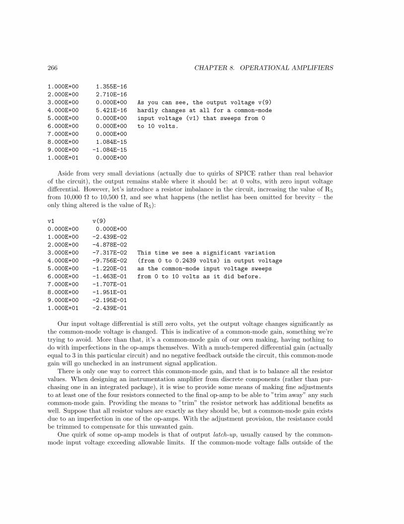
266 CHAPTER 8. OPERATIONAL AMPLIFIERS
1.000E+00 1.355E-16
2.000E+00 2.710E-16
3.000E+00 0.000E+00 As you can see, the output voltage v(9)
4.000E+00 5.421E-16 hardly changes at all for a common-mode
5.000E+00 0.000E+00 input voltage (v1) that sweeps from 0
6.000E+00 0.000E+00 to 10 volts.
7.000E+00 0.000E+00
8.000E+00 1.084E-15
9.000E+00 -1.084E-15
1.000E+01 0.000E+00
Aside from very small deviations (actually due to quirks of SPICE rather than real behaviorof the circuit), the output remains stable where it should be: at 0 volts, with zero input voltagedifferential. However, let’s introduce a resistor imbalance in the circuit, increasing the value of R5
from 10,000 Ω to 10,500 Ω, and see what happens (the netlist has been omitted for brevity – theonly thing altered is the value of R5):
v1 v(9)
0.000E+00 0.000E+00
1.000E+00 -2.439E-02
2.000E+00 -4.878E-02
3.000E+00 -7.317E-02 This time we see a significant variation
4.000E+00 -9.756E-02 (from 0 to 0.2439 volts) in output voltage
5.000E+00 -1.220E-01 as the common-mode input voltage sweeps
6.000E+00 -1.463E-01 from 0 to 10 volts as it did before.
7.000E+00 -1.707E-01
8.000E+00 -1.951E-01
9.000E+00 -2.195E-01
1.000E+01 -2.439E-01
Our input voltage differential is still zero volts, yet the output voltage changes significantly asthe common-mode voltage is changed. This is indicative of a common-mode gain, something we’retrying to avoid. More than that, it’s a common-mode gain of our own making, having nothing todo with imperfections in the op-amps themselves. With a much-tempered differential gain (actuallyequal to 3 in this particular circuit) and no negative feedback outside the circuit, this common-modegain will go unchecked in an instrument signal application.There is only one way to correct this common-mode gain, and that is to balance all the resistor
values. When designing an instrumentation amplifier from discrete components (rather than pur-chasing one in an integrated package), it is wise to provide some means of making fine adjustmentsto at least one of the four resistors connected to the final op-amp to be able to ”trim away” any suchcommon-mode gain. Providing the means to ”trim” the resistor network has additional benefits aswell. Suppose that all resistor values are exactly as they should be, but a common-mode gain existsdue to an imperfection in one of the op-amps. With the adjustment provision, the resistance couldbe trimmed to compensate for this unwanted gain.One quirk of some op-amp models is that of output latch-up, usually caused by the common-
mode input voltage exceeding allowable limits. If the common-mode voltage falls outside of the
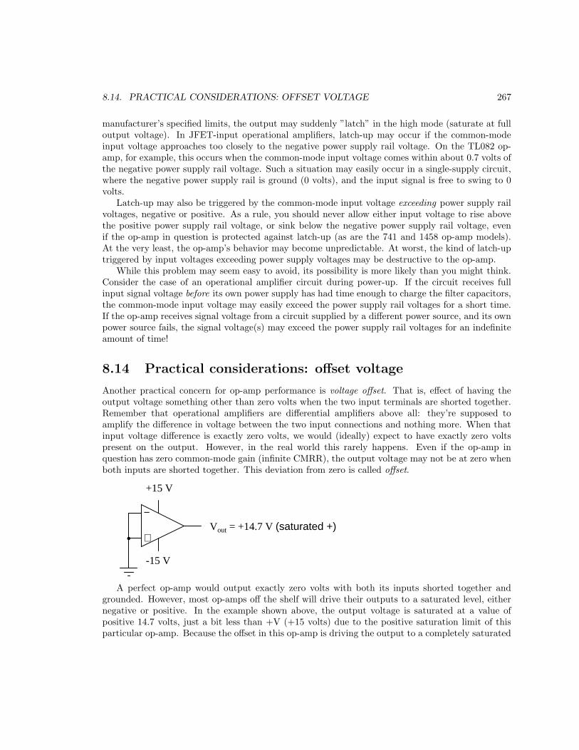
8.14. PRACTICAL CONSIDERATIONS: OFFSET VOLTAGE 267
manufacturer’s specified limits, the output may suddenly ”latch” in the high mode (saturate at fulloutput voltage). In JFET-input operational amplifiers, latch-up may occur if the common-modeinput voltage approaches too closely to the negative power supply rail voltage. On the TL082 op-amp, for example, this occurs when the common-mode input voltage comes within about 0.7 volts ofthe negative power supply rail voltage. Such a situation may easily occur in a single-supply circuit,where the negative power supply rail is ground (0 volts), and the input signal is free to swing to 0volts.Latch-up may also be triggered by the common-mode input voltage exceeding power supply rail
voltages, negative or positive. As a rule, you should never allow either input voltage to rise abovethe positive power supply rail voltage, or sink below the negative power supply rail voltage, evenif the op-amp in question is protected against latch-up (as are the 741 and 1458 op-amp models).At the very least, the op-amp’s behavior may become unpredictable. At worst, the kind of latch-uptriggered by input voltages exceeding power supply voltages may be destructive to the op-amp.While this problem may seem easy to avoid, its possibility is more likely than you might think.
Consider the case of an operational amplifier circuit during power-up. If the circuit receives fullinput signal voltage before its own power supply has had time enough to charge the filter capacitors,the common-mode input voltage may easily exceed the power supply rail voltages for a short time.If the op-amp receives signal voltage from a circuit supplied by a different power source, and its ownpower source fails, the signal voltage(s) may exceed the power supply rail voltages for an indefiniteamount of time!
8.14 Practical considerations: offset voltage
Another practical concern for op-amp performance is voltage offset. That is, effect of having theoutput voltage something other than zero volts when the two input terminals are shorted together.Remember that operational amplifiers are differential amplifiers above all: they’re supposed toamplify the difference in voltage between the two input connections and nothing more. When thatinput voltage difference is exactly zero volts, we would (ideally) expect to have exactly zero voltspresent on the output. However, in the real world this rarely happens. Even if the op-amp inquestion has zero common-mode gain (infinite CMRR), the output voltage may not be at zero whenboth inputs are shorted together. This deviation from zero is called offset.
−
+
+15 V
-15 V
Vout = +14.7 V (saturated +)
A perfect op-amp would output exactly zero volts with both its inputs shorted together andgrounded. However, most op-amps off the shelf will drive their outputs to a saturated level, eithernegative or positive. In the example shown above, the output voltage is saturated at a value ofpositive 14.7 volts, just a bit less than +V (+15 volts) due to the positive saturation limit of thisparticular op-amp. Because the offset in this op-amp is driving the output to a completely saturated

268 CHAPTER 8. OPERATIONAL AMPLIFIERS
point, there’s no way of telling how much voltage offset is present at the output. If the +V/-V splitpower supply was of a high enough voltage, who knows, maybe the output would be several hundredvolts one way or the other due to the effects of offset!
For this reason, offset voltage is usually expressed in terms of the equivalent amount of inputvoltage differential producing this effect. In other words, we imagine that the op-amp is perfect (nooffset whatsoever), and a small voltage is being applied in series with one of the inputs to force theoutput voltage one way or the other away from zero. Being that op-amp differential gains are sohigh, the figure for ”input offset voltage” doesn’t have to be much to account for what we see withshorted inputs:
−
+
+15 V
-15 V
Vout = +14.7 V (saturated +)
Input offset voltage(internal to the real op-amp,external to this ideal op-amp)
Offset voltage will tend to introduce slight errors in any op-amp circuit. So how do we compensatefor it? Unlike common-mode gain, there are usually provisions made by the manufacturer to trimthe offset of a packaged op-amp. Usually, two extra terminals on the op-amp package are reservedfor connecting an external ”trim” potentiometer. These connection points are labeled offset nulland are used in this general way:
−
+
Potentiometer adjusted so thatVout = 0 volts with inputs shorted together
Vout
+15 V
-15 V
On single op-amps such as the 741 and 3130, the offset null connection points are pins 1 and 5on the 8-pin DIP package. Other models of op-amp may have the offset null connections located ondifferent pins, and/or require a slightly difference configuration of trim potentiometer connection.Some op-amps don’t provide offset null pins at all! Consult the manufacturer’s specifications fordetails.
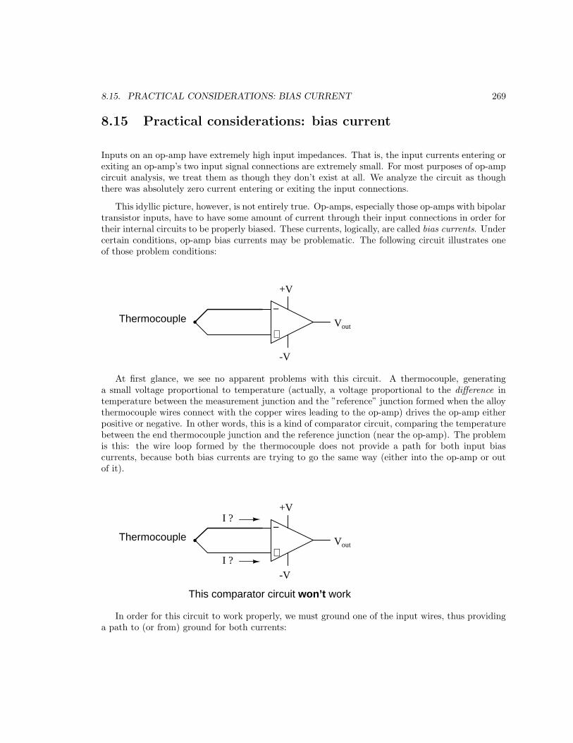
8.15. PRACTICAL CONSIDERATIONS: BIAS CURRENT 269
8.15 Practical considerations: bias current
Inputs on an op-amp have extremely high input impedances. That is, the input currents entering orexiting an op-amp’s two input signal connections are extremely small. For most purposes of op-ampcircuit analysis, we treat them as though they don’t exist at all. We analyze the circuit as thoughthere was absolutely zero current entering or exiting the input connections.
This idyllic picture, however, is not entirely true. Op-amps, especially those op-amps with bipolartransistor inputs, have to have some amount of current through their input connections in order fortheir internal circuits to be properly biased. These currents, logically, are called bias currents. Undercertain conditions, op-amp bias currents may be problematic. The following circuit illustrates oneof those problem conditions:
−
+Thermocouple Vout
+V
-V
At first glance, we see no apparent problems with this circuit. A thermocouple, generatinga small voltage proportional to temperature (actually, a voltage proportional to the difference intemperature between the measurement junction and the ”reference” junction formed when the alloythermocouple wires connect with the copper wires leading to the op-amp) drives the op-amp eitherpositive or negative. In other words, this is a kind of comparator circuit, comparing the temperaturebetween the end thermocouple junction and the reference junction (near the op-amp). The problemis this: the wire loop formed by the thermocouple does not provide a path for both input biascurrents, because both bias currents are trying to go the same way (either into the op-amp or outof it).
−
+Thermocouple Vout
+V
-V
I ?
I ?
This comparator circuit won’t work
In order for this circuit to work properly, we must ground one of the input wires, thus providinga path to (or from) ground for both currents:
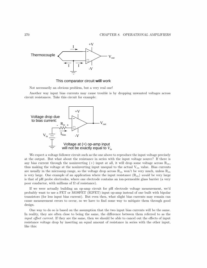
270 CHAPTER 8. OPERATIONAL AMPLIFIERS
−
+Thermocouple Vout
+V
-VI I
I
This comparator circuit will work
Not necessarily an obvious problem, but a very real one!
Another way input bias currents may cause trouble is by dropping unwanted voltages acrosscircuit resistances. Take this circuit for example:
−
+Vout
+V
-V
- +Rin
VinIbias
Voltage drop dueto bias current:
Voltage at (+) op-amp inputwill not be exactly equal to Vin
We expect a voltage follower circuit such as the one above to reproduce the input voltage preciselyat the output. But what about the resistance in series with the input voltage source? If there isany bias current through the noninverting (+) input at all, it will drop some voltage across Rin,thus making the voltage at the noninverting input unequal to the actual Vin value. Bias currentsare usually in the microamp range, so the voltage drop across Rin won’t be very much, unless Rin
is very large. One example of an application where the input resistance (Rin) would be very largeis that of pH probe electrodes, where one electrode contains an ion-permeable glass barrier (a verypoor conductor, with millions of Ω of resistance).
If we were actually building an op-amp circuit for pH electrode voltage measurement, we’dprobably want to use a FET or MOSFET (IGFET) input op-amp instead of one built with bipolartransistors (for less input bias current). But even then, what slight bias currents may remain cancause measurement errors to occur, so we have to find some way to mitigate them through gooddesign.
One way to do so is based on the assumption that the two input bias currents will be the same.In reality, they are often close to being the same, the difference between them referred to as theinput offset current. If they are the same, then we should be able to cancel out the effects of inputresistance voltage drop by inserting an equal amount of resistance in series with the other input,like this:

8.15. PRACTICAL CONSIDERATIONS: BIAS CURRENT 271
−
+Vout
+V
-V
- +
VinIbias
Rin(-)
Rin(+)
Ibias
- +
With the additional resistance added to the circuit, the output voltage will be closer to Vin thanbefore, even if there is some offset between the two input currents.For both inverting and noninverting amplifier circuits, the bias current compensating resistor is
placed in series with the noninverting (+) input to compensate for bias current voltage drops in thedivider network:
−
+Vout
Vin
Rcomp
R1 R2
Noninverting amplifier withcompensating resistor
Rcomp = R1 // R2
−
+Vout
Vin
Rcomp
R1 R2
compensating resistor
Rcomp = R1 // R2
Inverting amplifier with

272 CHAPTER 8. OPERATIONAL AMPLIFIERS
In either case, the compensating resistor value is determined by calculating the parallel resistancevalue of R1 and R2. Why is the value equal to the parallel equivalent of R1 and R2? When usingthe Superposition Theorem to figure how much voltage drop will be produced by the inverting (-)input’s bias current, we treat the bias current as though it were coming from a current source insidethe op-amp and short-circuit all voltage sources (Vin and Vout). This gives two parallel paths forbias current (through R1 and through R2, both to ground). We want to duplicate the bias current’seffect on the noninverting (+) input, so the resistor value we choose to insert in series with thatinput needs to be equal to R1 in parallel with R2.
A related problem, occasionally experienced by students just learning to build operational ampli-fier circuits, is caused by a lack of a common ground connection to the power supply. It is imperativeto proper op-amp function that some terminal of the DC power supply be common to the ”ground”connection of the input signal(s). This provides a complete path for the bias currents, feedbackcurrent(s), and for the load (output) current. Take this circuit illustration, for instance, showing aproperly grounded power supply:
null
-
+
+V
-V
6 V
R1 R2
1 kΩ 1 kΩ
Here, arrows denote the path of electron flow through the power supply batteries, both forpowering the op-amp’s internal circuitry (the ”potentiometer” inside of it that controls outputvoltage), and for powering the feedback loop of resistors R1 and R2. Suppose, however, that theground connection for this ”split” DC power supply were to be removed. The effect of doing this isprofound:

8.15. PRACTICAL CONSIDERATIONS: BIAS CURRENT 273
null
-
+
+V
-V
6 V
R1 R2
1 kΩ 1 kΩ
brokenconnection
A power supply ground is essential to circuit operation!
No electrons may flow in or out of the op-amp’s output terminal, because the pathway to thepower supply is a ”dead end.” Thus, no electrons flow through the ground connection to the left ofR1, neither through the feedback loop. This effectively renders the op-amp useless: it can neithersustain current through the feedback loop, nor through a grounded load, since there is no connectionfrom any point of the power supply to ground.
The bias currents are also stopped, because they rely on a path to the power supply and backto the input source through ground. The following diagram shows the bias currents (only), as theygo through the input terminals of the op-amp, through the base terminals of the input transistors,and eventually through the power supply terminal(s) and back to ground.

274 CHAPTER 8. OPERATIONAL AMPLIFIERS
-
+
+V
6 V
Ibias
-V
Ibias
Bias current paths shown, through power supply
Without a ground reference on the power supply, the bias currents will have no complete pathfor a circuit, and they will halt. Since bipolar junction transistors are current-controlled devices,this renders the input stage of the op-amp useless as well, as both input transistors will be forcedinto cutoff by the complete lack of base current.
• REVIEW:
• Op-amp inputs usually conduct very small currents, called bias currents, needed to properlybias the first transistor amplifier stage internal to the op-amps’ circuitry. Bias currents aresmall (in the microamp range), but large enough to cause problems in some applications.
• Bias currents in both inputs must have paths to flow to either one of the power supply ”rails”or to ground. It is not enough to just have a conductive path from one input to the other.
• To cancel any offset voltages caused by bias current flowing through resistances, just add anequivalent resistance in series with the other op-amp input (called a compensating resistor).This corrective measure is based on the assumption that the two input bias currents will beequal.
• Any inequality between bias currents in an op-amp constitutes what is called an input offsetcurrent.
• It is essential for proper op-amp operation that there be a ground reference on some terminalof the power supply, to form complete paths for bias currents, feedback current(s), and loadcurrent.
8.16 Practical considerations: drift
Being semiconductor devices, op-amps are subject to slight changes in behavior with changes in op-erating temperature. Any changes in op-amp performance with temperature fall under the category

8.17. PRACTICAL CONSIDERATIONS: FREQUENCY RESPONSE 275
of op-amp drift. Drift parameters can be specified for bias currents, offset voltage, and the like.Consult the manufacturer’s data sheet for specifics on any particular op-amp.
To minimize op-amp drift, we can select an op-amp made to have minimum drift, and/or wecan do our best to keep the operating temperature as stable as possible. The latter action mayinvolve providing some form of temperature control for the inside of the equipment housing theop-amp(s). This is not as strange as it may first seem. Laboratory-standard precision voltagereference generators, for example, are sometimes known to employ ”ovens” for keeping their sensitivecomponents (such as zener diodes) at constant temperatures. If extremely high accuracy is desiredover the usual factors of cost and flexibility, this may be an option worth looking at.
• REVIEW:
• Op-amps, being semiconductor devices, are susceptible to variations in temperature. Anyvariations in amplifier performance resulting from changes in temperature is known as drift.Drift is best minimized with environmental temperature control.
8.17 Practical considerations: frequency response
With their incredibly high differential voltage gains, op-amps are prime candidates for a phenomenonknown as feedback oscillation. You’ve probably heard the equivalent audio effect when the volume(gain) on a public-address or other microphone amplifier system is turned too high: that high pitchedsqueal resulting from the sound waveform ”feeding back” through the microphone to be amplifiedagain. An op-amp circuit can manifest this same effect, with the feedback happening electricallyrather than audibly.
A case example of this is seen in the 3130 op-amp, if it is connected as a voltage follower with thebare minimum of wiring connections (the two inputs, output, and the power supply connections).The output of this op-amp will self-oscillate due to its high gain, no matter what the input voltage. Tocombat this, a small compensation capacitor must be connected to two specially-provided terminalson the op-amp. The capacitor provides a high-impedance path for negative feedback to occur withinthe op-amp’s circuitry, thus decreasing the AC gain and inhibiting unwanted oscillations. If theop-amp is being used to amplify high-frequency signals, this compensation capacitor may not beneeded, but it is absolutely essential for DC or low-frequency AC signal operation.
Some op-amps, such as the model 741, have a compensation capacitor built in to minimize theneed for external components. This improved simplicity is not without a cost: due to that capacitor’spresence inside the op-amp, the negative feedback tends to get stronger as the operating frequencyincreases (that capacitor’s reactance decreases with higher frequencies). As a result, the op-amp’sdifferential voltage gain decreases as frequency goes up: it becomes a less effective amplifier at higherfrequencies.
Op-amp manufacturers will publish the frequency response curves for their products. Since asufficiently high differential gain is absolutely essential to good feedback operation in op-amp circuits,the gain/frequency response of an op-amp effectively limits its ”bandwidth” of operation. The circuitdesigner must take this into account if good performance is to be maintained over the required rangeof signal frequencies.
• REVIEW:

276 CHAPTER 8. OPERATIONAL AMPLIFIERS
• Due to capacitances within op-amps, their differential voltage gain tends to decrease as theinput frequency increases. Frequency response curves for op-amps are available from themanufacturer.
8.18 Operational amplifier models
While mention of operational amplifiers typically provokes visions of semiconductor devices built asintegrated circuits on a miniature silicon chip, the first op-amps were actually vacuum tube circuits.The first commercial, general purpose operational amplifier was manufactured by the George A.Philbrick Researches, Incorporated, in 1952. Designated the K2-W, it was built around two twin-triode tubes mounted in an assembly with an octal (8-pin) socket for easy installation and servicingin electronic equipment chassis of that era. The assembly looked something like this:
The Philbrick Researchesop-amp, model K2-W
GAP/RMODELK2-W
4 inchesapprox.
The schematic diagram shows the two tubes, along with ten resistors and two capacitors, a fairlysimple circuit design even by 1952 standards:

8.18. OPERATIONAL AMPLIFIER MODELS 277
12AX7
+300 V
220 kΩ
220 kΩ
-300 V
Inverting (-)input
Noninverting (+)input
1 MΩ
2.2 MΩ
510 kΩ
120 kΩ 4.7 MΩ221 kΩ
9.1 kΩ
12AX7
680 kΩ
7.5 pF
500 pF
NE-68
Output
The Philbrick Researches op-amp, model K2-W
In case you’re unfamiliar with the operation of vacuum tubes, they operate similarly to N-channeldepletion-type IGFET transistors: that is, they conduct more current when the control grid (thedashed line) is made more positive with respect to the cathode (the bent line near the bottom of thetube symbol), and conduct less current when the control grid is made less positive (or more negative)than the cathode. The twin triode tube on the left functions as a differential pair, converting thedifferential inputs (inverting and noninverting input voltage signals) into a single, amplified voltagesignal which is then fed to the control grid of the left triode of the second triode pair through avoltage divider (1 MΩ −− 2.2 MΩ). That triode amplifies and inverts the output of the differentialpair for a larger voltage gain, then the amplified signal is coupled to the second triode of the samedual-triode tube in a noninverting amplifier configuration for a larger current gain. The two neon”glow tubes” act as voltage regulators, similar to the behavior of semiconductor zener diodes, toprovide a bias voltage in the coupling between the two single-ended amplifier triodes.
With a dual-supply voltage of +300/-300 volts, this op-amp could only swing its output +/-50 volts, which is very poor by today’s standards. It had an open-loop voltage gain of 15,000 to20,000, a slew rate of +/- 12 volts/µsecond, a maximum output current of 1 mA, a quiescent powerconsumption of over 3 watts (not including power for the tubes’ filaments!), and cost about $24 in1952 dollars. Better performance could have been attained using a more sophisticated circuit design,but only at the expense of greater power consumption, greater cost, and decreased reliability.
With the advent of solid-state transistors, op-amps with far less quiescent power consumptionand increased reliability became feasible, but many of the other performance parameters remainedabout the same. Take for instance Philbrick’s model P55A, a general-purpose solid-state op-ampcirca 1966. The P55A sported an open-loop gain of 40,000, a slew rate of 1.5 volt/µsecond and anoutput swing of +/- 11 volts (at a power supply voltage of +/- 15 volts), a maximum output currentof 2.2 mA, and a cost of $49 (or about $21 for the ”utility grade” version). The P55A, as well as otherop-amps in Philbrick’s lineup of the time, was of discrete-component construction, its constituenttransistors, resistors, and capacitors housed in a solid ”brick” resembling a large integrated circuitpackage.
It isn’t very difficult to build a crude operational amplifier using discrete components. A

278 CHAPTER 8. OPERATIONAL AMPLIFIERS
schematic of one such circuit is shown here:
Q1 Q2
Q3 Q4
Q5 Q6
-V
+V
(-) inputinput (+)
Output
A simple operationalamplifier made fromdiscrete components
While its performance is rather dismal by modern standards, it demonstrates that complexityis not necessary to create a minimally functional op-amp. Transistors Q3 and Q4 form the heart ofanother differential pair circuit, the semiconductor equivalent of the first triode tube in the K2-Wschematic. As it was in the vacuum tube circuit, the purpose of a differential pair is to amplify andconvert a differential voltage between the two input terminals to a single-ended output voltage.
With the advent of integrated-circuit (IC) technology, op-amp designs experienced a dramaticincrease in performance, reliability, density, and economy. Between the years of 1964 and 1968, theFairchild corporation introduced three models of IC op-amps: the 702, 709, and the still-popular741. While the 741 is now considered outdated in terms of performance, it is still a favorite amonghobbyists for its simplicity and fault tolerance (short-circuit protection on the output, for instance).Personal experience abusing many 741 op-amps has led me to the conclusion that it is a hard chipto kill . . .
The internal schematic diagram for a model 741 op-amp is as follows:

8.18. OPERATIONAL AMPLIFIER MODELS 279
Q3 Q4
Q1 Q2
Q5 Q6
R1 R2R3 R4
Q7
Q10
Q8 Q9 Q12
Q11
R5(+) input
(-) input
Q13
offset nulloffset null
+V
-V
Q23
Q16
R9 R8
C1
Q17
Q24
Q22
Q19
Q18
R10
Q15
Q14
R6
OutputR7
Q21
Q20
R11
Internal schematic of a model 741 operational amplifier
By integrated circuit standards, the 741 is a very simple device: an example of small-scaleintegration, or SSI technology. It would be no small matter to build this circuit using discretecomponents, so you can see the advantages of even the most primitive integrated circuit technologyover discrete components where high parts counts are involved.For the hobbyist, student, or engineer desiring greater performance, there are literally hundreds
of op-amp models to choose from. Many sell for less than a dollar apiece, even retail! Special-purpose instrumentation and radio-frequency (RF) op-amps may be quite a bit more expensive.In this section I will showcase several popular and affordable op-amps, comparing and contrastingtheir performance specifications. The venerable 741 is included as a ”benchmark” for comparison,although it is, as I said before, considered an obsolete design.
OPAMP NUMBER OF PWR SUPPLY BAND- MAX. BIAS SLEW MAX. OUT
MODEL AMPLIFIERS VOLTAGE WIDTH CURRENT RATE CURRENT
NUMBER IN PACKAGE MIN./MAX. (MHz) (nA) (V/us) (mA)
TL082 2 12 / 36 4 8 13 17
LM301A 1 10 / 36 1 250 0.5 25
LM318 1 10 / 40 15 500 70 20
LM324 4 3 / 32 1 45 0.25 20
LF353 2 12 / 36 4 8 13 20
LF356 1 10 / 36 5 8 12 25
LF411 1 10 / 36 4 20 15 25
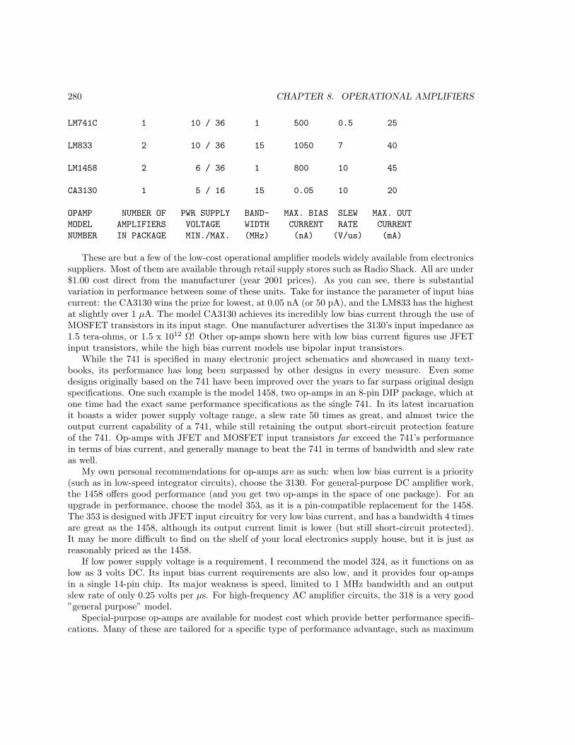
280 CHAPTER 8. OPERATIONAL AMPLIFIERS
LM741C 1 10 / 36 1 500 0.5 25
LM833 2 10 / 36 15 1050 7 40
LM1458 2 6 / 36 1 800 10 45
CA3130 1 5 / 16 15 0.05 10 20
OPAMP NUMBER OF PWR SUPPLY BAND- MAX. BIAS SLEW MAX. OUT
MODEL AMPLIFIERS VOLTAGE WIDTH CURRENT RATE CURRENT
NUMBER IN PACKAGE MIN./MAX. (MHz) (nA) (V/us) (mA)
These are but a few of the low-cost operational amplifier models widely available from electronicssuppliers. Most of them are available through retail supply stores such as Radio Shack. All are under$1.00 cost direct from the manufacturer (year 2001 prices). As you can see, there is substantialvariation in performance between some of these units. Take for instance the parameter of input biascurrent: the CA3130 wins the prize for lowest, at 0.05 nA (or 50 pA), and the LM833 has the highestat slightly over 1 µA. The model CA3130 achieves its incredibly low bias current through the use ofMOSFET transistors in its input stage. One manufacturer advertises the 3130’s input impedance as1.5 tera-ohms, or 1.5 x 10¹² Ω! Other op-amps shown here with low bias current figures use JFETinput transistors, while the high bias current models use bipolar input transistors.While the 741 is specified in many electronic project schematics and showcased in many text-
books, its performance has long been surpassed by other designs in every measure. Even somedesigns originally based on the 741 have been improved over the years to far surpass original designspecifications. One such example is the model 1458, two op-amps in an 8-pin DIP package, which atone time had the exact same performance specifications as the single 741. In its latest incarnationit boasts a wider power supply voltage range, a slew rate 50 times as great, and almost twice theoutput current capability of a 741, while still retaining the output short-circuit protection featureof the 741. Op-amps with JFET and MOSFET input transistors far exceed the 741’s performancein terms of bias current, and generally manage to beat the 741 in terms of bandwidth and slew rateas well.My own personal recommendations for op-amps are as such: when low bias current is a priority
(such as in low-speed integrator circuits), choose the 3130. For general-purpose DC amplifier work,the 1458 offers good performance (and you get two op-amps in the space of one package). For anupgrade in performance, choose the model 353, as it is a pin-compatible replacement for the 1458.The 353 is designed with JFET input circuitry for very low bias current, and has a bandwidth 4 timesare great as the 1458, although its output current limit is lower (but still short-circuit protected).It may be more difficult to find on the shelf of your local electronics supply house, but it is just asreasonably priced as the 1458.If low power supply voltage is a requirement, I recommend the model 324, as it functions on as
low as 3 volts DC. Its input bias current requirements are also low, and it provides four op-ampsin a single 14-pin chip. Its major weakness is speed, limited to 1 MHz bandwidth and an outputslew rate of only 0.25 volts per µs. For high-frequency AC amplifier circuits, the 318 is a very good”general purpose” model.Special-purpose op-amps are available for modest cost which provide better performance specifi-
cations. Many of these are tailored for a specific type of performance advantage, such as maximum

8.19. DATA 281
bandwidth or minimum bias current. Take for instance these op-amps, both designed for highbandwidth:
OPAMP NUMBER OF PWR SUPPLY BAND- MAX. BIAS SLEW MAX. OUT
MODEL AMPLIFIERS VOLTAGE WIDTH CURRENT RATE CURRENT
NUMBER IN PACKAGE MIN./MAX. (MHz) (nA) (V/us) (mA)
CLC404 1 10 / 14 232 44,000 2600 70
CLC425 1 5 / 14 1,900 40,000 350 90
The CLC404 lists at $21.80 (almost as much as George Philbrick’s first commercial op-amp,albeit without correction for inflation), while the CLC425 is quite a bit less expensive at $3.23 perunit. In both cases high speed is achieved at the expense of high bias currents and restrictive powersupply voltage ranges. Here are some other op-amps, designed for high power output:
OPAMP NUMBER OF PWR SUPPLY BAND- MAX. BIAS SLEW MAX. OUT
MODEL AMPLIFIERS VOLTAGE WIDTH CURRENT RATE CURRENT
NUMBER IN PACKAGE MIN./MAX. (MHz) (nA) (V/us) (mA)
LM12CL 1 15 / 80 0.7 1,000 9 13,000
LM7171 1 5.5 / 36 200 12,000 4100 100
Yes, the LM12CL actually has an output current rating of 13 amps (13,000 milliamps)! It listsat $14.40, which is not a lot of money, considering the raw power of the device. The LM7171, onthe other hand, trades high current output ability for fast voltage output ability (a high slew rate).It lists at $1.19, about as low as some ”general purpose” op-amps.Amplifier packages may also be purchased as complete application circuits as opposed to bare
operational amplifiers. The Burr-Brown and Analog Devices corporations, for example, both longknown for their precision amplifier product lines, offer instrumentation amplifiers in pre-designedpackages as well as other specialized amplifier devices. In designs where high precision and repeata-bility after repair is important, it might be advantageous for the circuit designer to choose such apre-engineered amplifier ”block” rather than build the circuit from individual op-amps. Of course,these units typically cost quite a bit more than individual op-amps.
8.19 Data
Parametrical data for all semiconductor op-amp models except the CA3130 comes from NationalSemiconductor’s online resources, available at this website: (http://www.national.com). Data forthe CA3130 comes from Harris Semiconductor’s CA3130/CA3130A datasheet (file number 817.4).

282 CHAPTER 8. OPERATIONAL AMPLIFIERS

Chapter 9
PRACTICAL ANALOGSEMICONDUCTOR CIRCUITS
Contents
9.1 Power supply circuits – INCOMPLETE . . . . . . . . . . . . . . . . . . 283
9.1.1 Unregulated . . . . . . . . . . . . . . . . . . . . . . . . . . . . . . . . . . . 283
9.1.2 Linear regulated . . . . . . . . . . . . . . . . . . . . . . . . . . . . . . . . 284
9.1.3 Switching . . . . . . . . . . . . . . . . . . . . . . . . . . . . . . . . . . . . 284
9.1.4 Ripple regulated . . . . . . . . . . . . . . . . . . . . . . . . . . . . . . . . 285
9.2 Amplifier circuits – PENDING . . . . . . . . . . . . . . . . . . . . . . . 285
9.3 Oscillator circuits – PENDING . . . . . . . . . . . . . . . . . . . . . . . 285
9.4 Phase-locked loops – PENDING . . . . . . . . . . . . . . . . . . . . . . 285
9.5 Radio circuits – PENDING . . . . . . . . . . . . . . . . . . . . . . . . . 285
9.6 Computational circuits . . . . . . . . . . . . . . . . . . . . . . . . . . . . 285
9.7 Measurement circuits – PENDING . . . . . . . . . . . . . . . . . . . . 307
9.8 Control circuits – PENDING . . . . . . . . . . . . . . . . . . . . . . . . 307
9.9 Contributors . . . . . . . . . . . . . . . . . . . . . . . . . . . . . . . . . . 307
*** INCOMPLETE ***
9.1 Power supply circuits – INCOMPLETE
There are three major kinds of power supplies: unregulated (also called brute force), linear regulated,and switching. A fourth type of power supply circuit called the ripple-regulated, is a hybrid betweenthe ”brute force” and ”switching” designs, and merits a subsection to itself.
9.1.1 Unregulated
An unregulated power supply is the most rudimentary type, consisting of a transformer, rectifier,and low-pass filter. These power supplies typically exhibit a lot of ripple voltage (i.e. rapidly-varying
283

284 CHAPTER 9. PRACTICAL ANALOG SEMICONDUCTOR CIRCUITS
instability) and other AC ”noise” superimposed on the DC power. If the input voltage varies, theoutput voltage will vary by a proportional amount. The advantage of an unregulated supply is thatit’s cheap, simple, and efficient.
9.1.2 Linear regulated
A linear regulated supply is simply a ”brute force” (unregulated) power supply followed by a tran-sistor circuit operating in its ”active,” or ”linear” mode, hence the name linear regulator. (Obviousin retrospect, isn’t it?) A typical linear regulator is designed to output a fixed voltage for a widerange of input voltages, and it simply drops any excess input voltage to allow a maximum outputvoltage to the load. This excess voltage drop results in significant power dissipation in the form ofheat. If the input voltage gets too low, the transistor circuit will lose regulation, meaning that itwill fail to keep the voltage steady. It can only drop excess voltage, not make up for a deficiencyin voltage from the brute force section of the circuit. Therefore, you have to keep the input voltageat least 1 to 3 volts higher than the desired output, depending on the regulator type. This meansthe power equivalent of at least 1 to 3 volts multiplied by the full load current will be dissipatedby the regulator circuit, generating a lot of heat. This makes linear regulated power supplies ratherinefficient. Also, to get rid of all that heat they have to use large heat sinks which makes them large,heavy, and expensive.
9.1.3 Switching
A switching regulated power supply (”switcher”) is an effort to realize the advantages of bothbrute force and linear regulated designs (small, efficient, and cheap, but also ”clean,” stable outputvoltage). Switching power supplies work on the principle of rectifying the incoming AC power linevoltage into DC, re-converting it into high-frequency square-wave AC through transistors operatedas on/off switches, stepping that AC voltage up or down by using a lightweight transformer, thenrectifying the transformer’s AC output into DC and filtering for final output. Voltage regulationis achieved by altering the ”duty cycle” of the DC-to-AC inversion on the transformer’s primaryside. In addition to lighter weight because of a smaller transformer core, switchers have anothertremendous advantage over the prior two designs: this type of power supply can be made so totallyindependent of the input voltage that it can work on any electric power system in the world; theseare called ”universal” power supplies.
The downside of switchers is that they are more complex, and due to their operation they tend togenerate a lot of high-frequency AC ”noise” on the power line. Most switchers also have significantripple voltage on their outputs. With the cheaper types, this noise and ripple can be as bad as foran unregulated power supply; such low-end switchers aren’t worthless, because they still provide astable average output voltage, and there’s the ”universal” input capability.
Expensive switchers are ripple-free and have noise nearly as low as for some a linear types; theseswitchers tend to be as expensive as linear supplies. The reason to use an expensive switcher insteadof a good linear is if you need universal power system compatibility or high efficiency. High efficiency,light weight, and small size are the reasons switching power supplies are almost universally used forpowering digital computer circuitry.

9.2. AMPLIFIER CIRCUITS – PENDING 285
9.1.4 Ripple regulated
A ripple-regulated power supply is an alternative to the linear regulated design scheme: a ”bruteforce” power supply (transformer, rectifier, filter) constitutes the ”front end” of the circuit, but atransistor operated strictly in its on/off (saturation/cutoff) modes transfers DC power to a largecapacitor as needed to maintain the output voltage between a high and a low setpoint. As inswitchers, the transistor in a ripple regulator never passes current while in its ”active,” or ”linear,”mode for any substantial length of time, meaning that very little energy will be wasted in the formof heat. However, the biggest drawback to this regulation scheme is the necessary presence of someripple voltage on the output, as the DC voltage varies between the two voltage control setpoints.Also, this ripple voltage varies in frequency depending on load current, which makes final filteringof the DC power more difficult.
Ripple regulator circuits tend to be quite a bit simpler than switcher circuitry, and they neednot handle the high power line voltages that switcher transistors must handle, making them saferto work on.
9.2 Amplifier circuits – PENDING
9.3 Oscillator circuits – PENDING
9.4 Phase-locked loops – PENDING
9.5 Radio circuits – PENDING
9.6 Computational circuits
When someone mentions the word ”computer,” a digital device is what usually comes to mind.Digital circuits represent numerical quantities in binary format: patterns of 1’s and 0’s representedby a multitude of transistor circuits operating in saturated or cutoff states. However, analog circuitrymay also be used to represent numerical quantities and perform mathematical calculations, by usingvariable voltage signals instead of discrete on/off states.
Here is a simple example of binary (digital) representation versus analog representation of thenumber ”twenty-five:”

286 CHAPTER 9. PRACTICAL ANALOG SEMICONDUCTOR CIRCUITS
1
2
4
8
16
32
16 + 8 + 1 = 25
A digital circuit representing the number 25:
100 V 050
100
Voltmeter
An analog circuit representing the number 25:
Digital circuits are very different from circuits built on analog principles. Digital computationalcircuits can be incredibly complex, and calculations must often be performed in sequential ”steps” toobtain a final answer, much as a human being would perform arithmetical calculations in steps withpencil and paper. Analog computational circuits, on the other hand, are quite simple in comparison,and perform their calculations in continuous, real-time fashion. There is a disadvantage to usinganalog circuitry to represent numbers, though: imprecision. The digital circuit shown above isrepresenting the number twenty-five, precisely. The analog circuit shown above may or may not beexactly calibrated to 25.000 volts, but is subject to ”drift” and error.In applications where precision is not critical, analog computational circuits are very practical
and elegant. Shown here are a few op-amp circuits for performing analog computation:
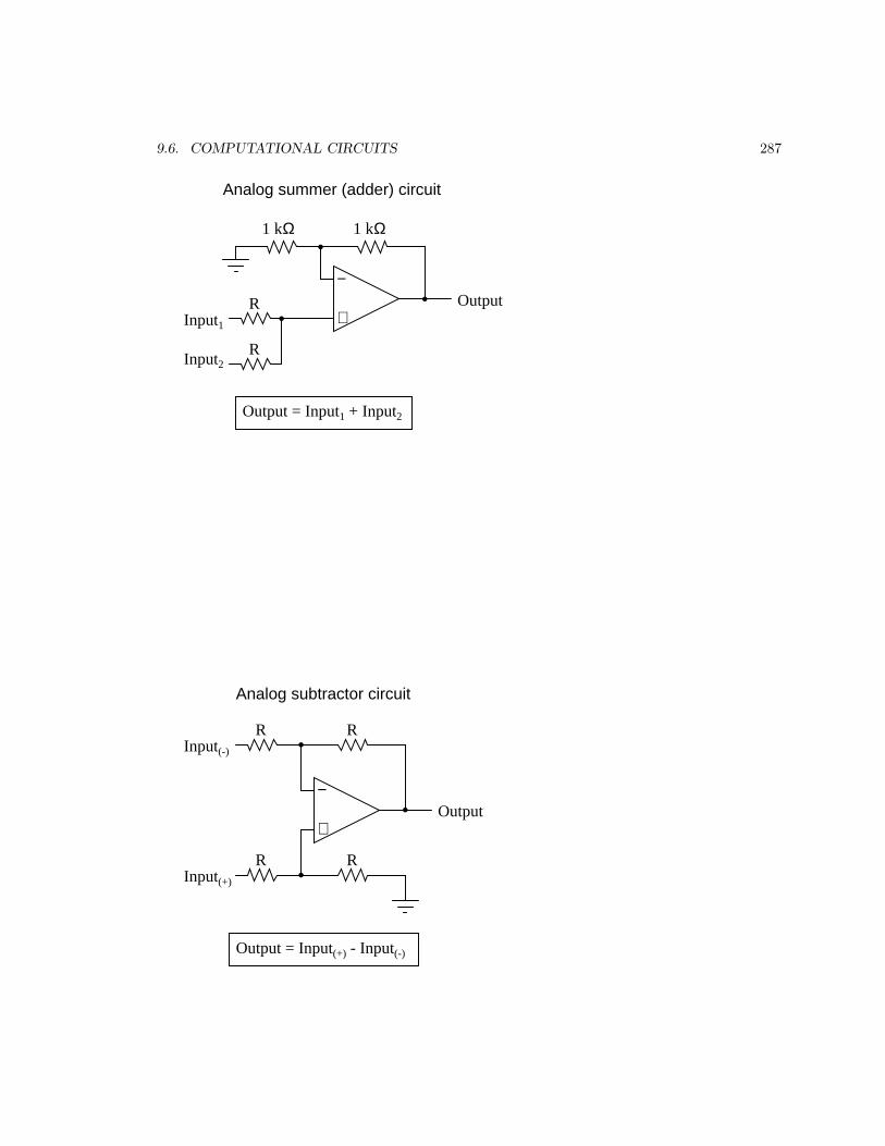
9.6. COMPUTATIONAL CIRCUITS 287
−
+
1 kΩ
R
R
Input1
Input2
Output
Analog summer (adder) circuit
Output = Input1 + Input2
1 kΩ
−
+
R R
R RInput(+)
Input(-)
Output
Analog subtractor circuit
Output = Input(+) - Input(-)

288 CHAPTER 9. PRACTICAL ANALOG SEMICONDUCTOR CIRCUITS
R
R
Input1
Input2
Output
Analog averager circuit
Output = Input1 + Input2
2
−
+ (Buffer optional)
Output−
+
Analog inverter (sign reverser) circuit
RRInput
Output = - Input
Output−
+ Input
K
Output = (K)(Input)
Analog "multiply-by-constant" circuit

9.6. COMPUTATIONAL CIRCUITS 289
Output
Output =
−
+ (Buffer optional)
Input
K
Input
K
Analog "divide-by-constant" circuit
Output−
+
Input
Output = - (K)(Input)
K
Analog inverting "multiply/divide-by-constant" circuit
Each of these circuits may be used in modular fashion to create a circuit capable of multiplecalculations. For instance, suppose that we needed to subtract a certain fraction of one variablefrom another variable. By combining a divide-by-constant circuit with a subtractor circuit, wecould obtain the required function:

290 CHAPTER 9. PRACTICAL ANALOG SEMICONDUCTOR CIRCUITS
−
+
R R
R R
Output
Divide-by-constant
K
−
+
Subtractor
Output = Input1 - Input2
K
Input1
Input2
Devices called analog computers used to be common in universities and engineering shops, wheredozens of op-amp circuits could be ”patched” together with removable jumper wires to model math-ematical statements, usually for the purpose of simulating some physical process whose underlyingequations were known. Digital computers have made analog computers all but obsolete, but ana-log computational circuitry cannot be beaten by digital in terms of sheer elegance and economy ofnecessary components.
Analog computational circuitry excels at performing the calculus operations integration anddifferentiation with respect to time, by using capacitors in an op-amp feedback loop. To fullyunderstand these circuits’ operation and applications, though, we must first grasp the meaning ofthese fundamental calculus concepts. Fortunately, the application of op-amp circuits to real-worldproblems involving calculus serves as an excellent means to teach basic calculus. In the words ofJohn I. Smith, taken from his outstanding textbook, Modern Operational Circuit Design:
”A note of encouragement is offered to certain readers: integral calculus is one of themathematical disciplines that operational [amplifier] circuitry exploits and, in the process,rather demolishes as a barrier to understanding.” (pg. 4)
Mr. Smith’s sentiments on the pedagogical value of analog circuitry as a learning tool for mathe-matics are not unique. Consider the opinion of engineer George Fox Lang, in an article he wrote forthe August 2000 issue of the journal Sound and Vibration, entitled, ”Analog was not a ComputerTrademark!”:
”Creating a real physical entity (a circuit) governed by a particular set of equationsand interacting with it provides unique insight into those mathematical statements. Thereis no better way to develop a ”gut feel” for the interplay between physics and mathematicsthan to experience such an interaction. The analog computer was a powerful interdis-ciplinary teaching tool; its obsolescence is mourned by many educators in a variety offields.” (pg. 23)

9.6. COMPUTATIONAL CIRCUITS 291
Differentiation is the first operation typically learned by beginning calculus students. Simplyput, differentiation is determining the instantaneous rate-of-change of one variable as it relates toanother. In analog differentiator circuits, the independent variable is time, and so the rates of changewe’re dealing with are rates of change for an electronic signal (voltage or current) with respect totime.
Suppose we were to measure the position of a car, traveling in a direct path (no turns), from itsstarting point. Let us call this measurement, x. If the car moves at a rate such that its distance from”start” increases steadily over time, its position will plot on a graph as a linear function (straightline):
x
x
Time
Position
If we were to calculate the derivative of the car’s position with respect to time (that is, determinethe rate-of-change of the car’s position with respect to time), we would arrive at a quantity repre-senting the car’s velocity. The differentiation function is represented by the fractional notation d/d,so when differentiating position (x ) with respect to time (t), we denote the result (the derivative)as dx/dt :
x
x
Time
Position
Time
dxdt
Velocity
For a linear graph of x over time, the derivate of position (dx/dt), otherwise and more commonlyknown as velocity, will be a flat line, unchanging in value. The derivative of a mathematical functionmay be graphically understood as its slope when plotted on a graph, and here we can see that the

292 CHAPTER 9. PRACTICAL ANALOG SEMICONDUCTOR CIRCUITS
position (x ) graph has a constant slope, which means that its derivative (dx/dt) must be constantover time.
Now, suppose the distance traveled by the car increased exponentially over time: that is, it beganits travel in slow movements, but covered more additional distance with each passing period in time.We would then see that the derivative of position (dx/dt), otherwise known as velocity (v), wouldnot be constant over time, but would increase:
x
x
Time
Position
Time
dxdt
Velocity
The height of points on the velocity graph correspond to the rates-of-change, or slope, of pointsat corresponding times on the position graph:
x
Time
Position
Time
dxdt
Velocity
What does this have to do with analog electronic circuits? Well, if we were to have an analogvoltage signal represent the car’s position (think of a huge potentiometer whose wiper was attachedto the car, generating a voltage proportional to the car’s position), we could connect a differentiatorcircuit to this signal and have the circuit continuously calculate the car’s velocity, displaying theresult via a voltmeter connected to the differentiator circuit’s output:

9.6. COMPUTATIONAL CIRCUITS 293
x
x
−
++
V-
+V
- dx
dt
Differentiator
Position
Velocity
Recall from the last chapter that a differentiator circuit outputs a voltage proportional to theinput voltage’s rate-of-change over time (d/dt). Thus, if the input voltage is changing over time ata constant rate, the output voltage will be at a constant value. If the car moves in such a way thatits elapsed distance over time builds up at a steady rate, then that means the car is traveling at aconstant velocity, and the differentiator circuit will output a constant voltage proportional to thatvelocity. If the car’s elapsed distance over time changes in a non-steady manner, the differentiatorcircuit’s output will likewise be non-steady, but always at a level representative of the input’s rate-of-change over time.
Note that the voltmeter registering velocity (at the output of the differentiator circuit) is con-nected in ”reverse” polarity to the output of the op-amp. This is because the differentiator circuitshown is inverting : outputting a negative voltage for a positive input voltage rate-of-change. Ifwe wish to have the voltmeter register a positive value for velocity, it will have to be connected tothe op-amp as shown. As impractical as it may be to connect a giant potentiometer to a movingobject such as an automobile, the concept should be clear: by electronically performing the calculusfunction of differentiation on a signal representing position, we obtain a signal representing velocity.
Beginning calculus students learn symbolic techniques for differentiation. However, this requiresthat the equation describing the original graph be known. For example, calculus students learnhow to take a function such as y = 3x and find its derivative with respect to x (d/dx ), 3, simplyby manipulating the equation. We may verify the accuracy of this manipulation by comparing thegraphs of the two functions:

294 CHAPTER 9. PRACTICAL ANALOG SEMICONDUCTOR CIRCUITS
y
x
y
xx = 1; slope = 3
x = 2; slope = 3x = 2.5; slope = 3
y = 3x
x = 1; y = 3
x = 2; y = 3
x = 2.5; y = 3
dx3x = 3
(y = 3)
d
Nonlinear functions such as y = 3x2 may also be differentiated by symbolic means. In this case,the derivative of y = 3x2 with respect to x is 6x :
y
x
y
x
dxy = 3x2
x = 0; slope = 0
x = 1; slope = 6
3x2 = 6x
(y = 6x)x = 2; slope = 12
x = 0; y = 0
x = 1; y = 6
x = 2; y = 12
d
In real life, though, we often cannot describe the behavior of any physical event by a simpleequation like y = 3x, and so symbolic differentiation of the type learned by calculus students may beimpossible to apply to a physical measurement. If someone wished to determine the derivative of ourhypothetical car’s position (dx/dt = velocity) by symbolic means, they would first have to obtainan equation describing the car’s position over time, based on position measurements taken froma real experiment – a nearly impossible task unless the car is operated under carefully controlledconditions leading to a very simple position graph. However, an analog differentiator circuit, byexploiting the behavior of a capacitor with respect to voltage, current, and time i = C(dv/dt),naturally differentiates any real signal in relation to time, and would be able to output a signalcorresponding to instantaneous velocity (dx/dt) at any moment. By logging the car’s position signalalong with the differentiator’s output signal using a chart recorder or other data acquisition device,both graphs would naturally present themselves for inspection and analysis.

9.6. COMPUTATIONAL CIRCUITS 295
We may take the principle of differentiation one step further by applying it to the velocity signalusing another differentiator circuit. In other words, use it to calculate the rate-of-change of velocity,which we know is the rate-of-change of position. What practical measure would we arrive at if wedid this? Think of this in terms of the units we use to measure position and velocity. If we wereto measure the car’s position from its starting point in miles, then we would probably express itsvelocity in units of miles per hour (dx/dt). If we were to differentiate the velocity (measured in milesper hour) with respect to time, we would end up with a unit of miles per hour per hour. Introductoryphysics classes teach students about the behavior of falling objects, measuring position in meters,velocity in meters per second, and change in velocity over time in meters per second, per second.This final measure is called acceleration: the rate of change of velocity over time:
x
x
Time
Position
Time
dxdt
Velocity
Time
Acceleration
d2x
dt2
Differentiation Differentiation
The expression d2x/dt2 is called the second derivative of position (x ) with regard to time (t). Ifwe were to connect a second differentiator circuit to the output of the first, the last voltmeter wouldregister acceleration:

296 CHAPTER 9. PRACTICAL ANALOG SEMICONDUCTOR CIRCUITS
x
x
−
++
V-
+V
- dx
dt
Differentiator
Position
Velocity
−
+
Differentiator
+V
-Acceleration
d2x
dt2
Deriving velocity from position, and acceleration from velocity, we see the principle of differen-tiation very clearly illustrated. These are not the only physical measurements related to each otherin this way, but they are, perhaps, the most common. Another example of calculus in action is therelationship between liquid flow (q) and liquid volume (v) accumulated in a vessel over time:
LT
Water
v = volume
dvdt
= flowWatersupply
A ”Level Transmitter” device mounted on a water storage tank provides a signal directly propor-tional to water level in the tank, which – if the tank is of constant cross-sectional area throughout itsheight – directly equates water volume stored. If we were to take this volume signal and differentiateit with respect to time (dv/dt), we would obtain a signal proportional to the water flow rate throughthe pipe carrying water to the tank. A differentiator circuit connected in such a way as to receivethis volume signal would produce an output signal proportional to flow, possibly substituting for a

9.6. COMPUTATIONAL CIRCUITS 297
flow-measurement device (”Flow Transmitter”) installed in the pipe.
Returning to the car experiment, suppose that our hypothetical car were equipped with a tacho-generator on one of the wheels, producing a voltage signal directly proportional to velocity. Wecould differentiate the signal to obtain acceleration with one circuit, like this:
x
−
++
V-
+V
-
Differentiator
Velocity
v
d2x
dt2Acceleration
dv
dt=
Gen+ -
By its very nature, the tachogenerator differentiates the car’s position with respect to time,generating a voltage proportional to how rapidly the wheel’s angular position changes over time.This provides us with a raw signal already representative of velocity, with only a single step ofdifferentiation needed to obtain an acceleration signal. A tachogenerator measuring velocity, ofcourse, is a far more practical example of automobile instrumentation than a giant potentiometermeasuring its physical position, but what we gain in practicality we lose in position measurement.No matter how many times we differentiate, we can never infer the car’s position from a velocitysignal. If the process of differentiation brought us from position to velocity to acceleration, thensomehow we need to perform the ”reverse” process of differentiation to go from velocity to position.Such a mathematical process does exist, and it is called integration. The ”integrator” circuit maybe used to perform this function of integration with respect to time:
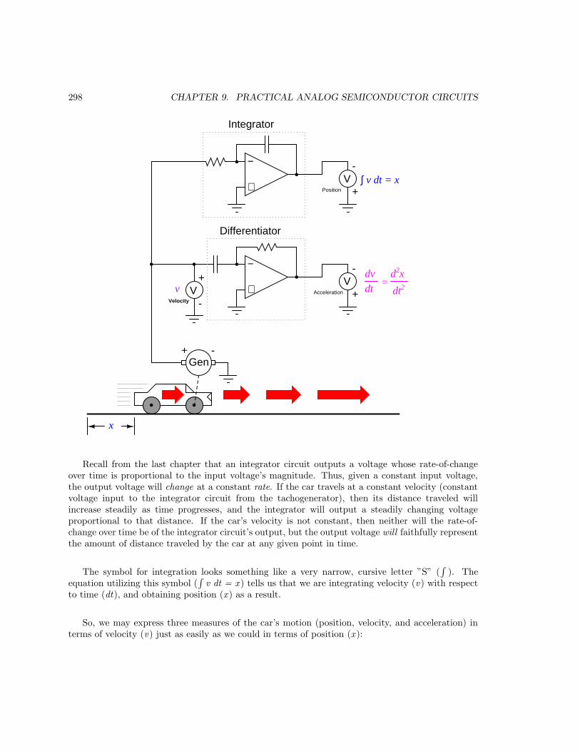
298 CHAPTER 9. PRACTICAL ANALOG SEMICONDUCTOR CIRCUITS
x
−
++
V-
+V
-
Differentiator
Velocity
v
d2x
dt2Acceleration
dv
dt=
Gen+ -
−
+
Integrator
+V
-
Position
∫ v dt = x
Recall from the last chapter that an integrator circuit outputs a voltage whose rate-of-changeover time is proportional to the input voltage’s magnitude. Thus, given a constant input voltage,the output voltage will change at a constant rate. If the car travels at a constant velocity (constantvoltage input to the integrator circuit from the tachogenerator), then its distance traveled willincrease steadily as time progresses, and the integrator will output a steadily changing voltageproportional to that distance. If the car’s velocity is not constant, then neither will the rate-of-change over time be of the integrator circuit’s output, but the output voltage will faithfully representthe amount of distance traveled by the car at any given point in time.
The symbol for integration looks something like a very narrow, cursive letter ”S” (∫). The
equation utilizing this symbol (∫v dt = x ) tells us that we are integrating velocity (v) with respect
to time (dt), and obtaining position (x ) as a result.
So, we may express three measures of the car’s motion (position, velocity, and acceleration) interms of velocity (v) just as easily as we could in terms of position (x ):

9.6. COMPUTATIONAL CIRCUITS 299
x
Time
Position
Time
Velocity
Time
Acceleration
DifferentiationIntegration
v dv
dt∫ v dt
If we had an accelerometer attached to the car, generating a signal proportional to the rateof acceleration or deceleration, we could (hypothetically) obtain a velocity signal with one step ofintegration, and a position signal with a second step of integration:
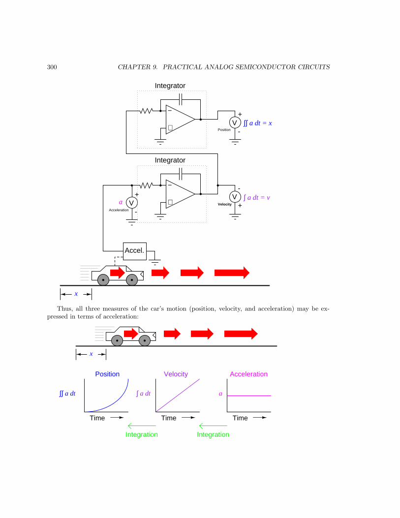
300 CHAPTER 9. PRACTICAL ANALOG SEMICONDUCTOR CIRCUITS
x
−
++
V-
+V
-
Velocity
Acceleration
−
+
Integrator
+V
-Position
Accel.
a
Integrator
∫ a dt = v
∫∫ a dt = x
Thus, all three measures of the car’s motion (position, velocity, and acceleration) may be ex-pressed in terms of acceleration:
x
Time
Position
Time
Velocity
Time
Acceleration
Integration Integration
a∫∫ a dt ∫ a dt

9.6. COMPUTATIONAL CIRCUITS 301
As you might have suspected, the process of integration may be illustrated in, and applied to,other physical systems as well. Take for example the water storage tank and flow example shownearlier. If flow rate is the derivative of tank volume with respect to time (q = dv/dt), then we couldalso say that volume is the integral of flow rate with respect to time:
Water
Watersupply
FT f = flow
∫ f dt = volume
If we were to use a ”Flow Transmitter” device to measure water flow, then by time-integration wecould calculate the volume of water accumulated in the tank over time. Although it is theoreticallypossible to use a capacitive op-amp integrator circuit to derive a volume signal from a flow signal,mechanical and digital electronic ”integrator” devices are more suitable for integration over longperiods of time, and find frequent use in the water treatment and distribution industries.
Just as there are symbolic techniques for differentiation, there are also symbolic techniques forintegration, although they tend to be more complex and varied. Applying symbolic integration toa real-world problem like the acceleration of a car, though, is still contingent on the availability ofan equation precisely describing the measured signal – often a difficult or impossible thing to derivefrom measured data. However, electronic integrator circuits perform this mathematical functioncontinuously, in real time, and for any input signal profile, thus providing a powerful tool for scientistsand engineers.
Having said this, there are caveats to the using calculus techniques to derive one type of mea-surement from another. Differentiation has the undesirable tendency of amplifying ”noise” foundin the measured variable, since the noise will typically appear as frequencies much higher than themeasured variable, and high frequencies by their very nature possess high rates-of-change over time.
To illustrate this problem, suppose we were deriving a measurement of car acceleration from thevelocity signal obtained from a tachogenerator with worn brushes or commutator bars. Points ofpoor contact between brush and commutator will produce momentary ”dips” in the tachogenerator’soutput voltage, and the differentiator circuit connected to it will interpret these dips as very rapidchanges in velocity. For a car moving at constant speed – neither accelerating nor decelerating – theacceleration signal should be 0 volts, but ”noise” in the velocity signal caused by a faulty tachogen-erator will cause the differentiated (acceleration) signal to contain ”spikes,” falsely indicating briefperiods of high acceleration and deceleration:

302 CHAPTER 9. PRACTICAL ANALOG SEMICONDUCTOR CIRCUITS
x
−
++
V-
+V
-
Differentiator
Velocity
v Acceleration
dv
dt
Gen+ -
Noise voltage present in a signal to be differentiated need not be of significant amplitude to causetrouble: all that is required is that the noise profile have fast rise or fall times. In other words, anyelectrical noise with a high dv/dt component will be problematic when differentiated, even if it is oflow amplitude.
It should be noted that this problem is not an artifact (an idiosyncratic error of the measur-ing/computing instrument) of the analog circuitry; rather, it is inherent to the process of differ-entiation. No matter how we might perform the differentiation, ”noise” in the velocity signal willinvariably corrupt the output signal. Of course, if we were differentiating a signal twice, as we didto obtain both velocity and acceleration from a position signal, the amplified noise signal output bythe first differentiator circuit will be amplified again by the next differentiator, thus compoundingthe problem:

9.6. COMPUTATIONAL CIRCUITS 303
x
x
−
++
V-
+V
- dx
dt
Differentiator
Position
Velocity
−
+
Differentiator
+V
-Acceleration
d2x
dt2
little noisemore noise even more noise!
Integration does not suffer from this problem, because integrators act as low-pass filters, atten-uating high-frequency input signals. In effect, all the high and low peaks resulting from noise onthe signal become averaged together over time, for a diminished net result. One might suppose,then, that we could avoid all trouble by measuring acceleration directly and integrating that signalto obtain velocity; in effect, calculating in ”reverse” from the way shown previously:

304 CHAPTER 9. PRACTICAL ANALOG SEMICONDUCTOR CIRCUITS
x
−
++
V-
+V
-
Velocity
Acceleration
Accel.
a
Integrator
∫ a dt = v
Unfortunately, following this methodology might lead us into other difficulties, one being acommon artifact of analog integrator circuits known as drift. All op-amps have some amount ofinput bias current, and this current will tend to cause a charge to accumulate on the capacitor inaddition to whatever charge accumulates as a result of the input voltage signal. In other words,all analog integrator circuits suffer from the tendency of having their output voltage ”drift” or”creep” even when there is absolutely no voltage input, accumulating error over time as a result.Also, imperfect capacitors will tend to lose their stored charge over time due to internal resistance,resulting in ”drift” toward zero output voltage. These problems are artifacts of the analog circuitry,and may be eliminated through the use of digital computation.
Circuit artifacts notwithstanding, possible errors may result from the integration of one mea-surement (such as acceleration) to obtain another (such as velocity) simply because of the wayintegration works. If the ”zero” calibration point of the raw signal sensor is not perfect, it will out-put a slight positive or negative signal even in conditions when it should output nothing. Considera car with an imperfectly calibrated accelerometer, or one that is influenced by gravity to detect aslight acceleration unrelated to car motion. Even with a perfect integrating computer, this sensorerror will cause the integrator to accumulate error, resulting in an output signal indicating a changeof velocity when the car is neither accelerating nor decelerating.

9.6. COMPUTATIONAL CIRCUITS 305
x
−
++
V-
+V
-
Velocity
Acceleration
Accel.
a
Integrator
∫ a dt = v
(no motion)
(slight positivevoltage)
(small rateof change)(calibration error)
As with differentiation, this error will also compound itself if the integrated signal is passed onto another integrator circuit, since the ”drifting” output of the first integrator will very soon presenta significant positive or negative signal for the next integrator to integrate. Therefore, care shouldbe taken when integrating sensor signals: if the ”zero” adjustment of the sensor is not perfect, theintegrated result will drift, even if the integrator circuit itself is perfect.
So far, the only integration errors discussed have been artificial in nature: originating fromimperfections in the circuitry and sensors. There also exists a source of error inherent to the processof integration itself, and that is the unknown constant problem. Beginning calculus students learnthat whenever a function is integrated, there exists an unknown constant (usually represented asthe variable C ) added to the result. This uncertainty is easiest to understand by comparing thederivatives of several functions differing only by the addition of a constant value:

306 CHAPTER 9. PRACTICAL ANALOG SEMICONDUCTOR CIRCUITS
y
x x
dx
y = 3x2
3x2 = 6xd
(y’ = 6x) y’
y = 3x2 - 6
y = 3x2 + 4
3x2 + 4 = 6x
3x2 - 6 = 6x
dxd
dxd
Note how each of the parabolic curves (y = 3x2 + C ) share the exact same shape, differingfrom each other in regard to their vertical offset. However, they all share the exact same derivativefunction: y’ = (d/dx)( 3x2 + C) = 6x, because they all share identical rates of change (slopes)at corresponding points along the x axis. While this seems quite natural and expected from theperspective of differentiation (different equations sharing a common derivative), it usually strikesbeginning students as odd from the perspective of integration, because there are multiple correctanswers for the integral of a function. Going from an equation to its derivative, there is only oneanswer, but going from that derivative back to the original equation leads us to a range of correctsolutions. In honor of this uncertainty, the symbolic function of integration is called the indefiniteintegral.
When an integrator performs live signal integration with respect to time, the output is the sumof the integrated input signal over time and an initial value of arbitrary magnitude, representingthe integrator’s pre-existing output at the time integration began. For example, if I integrate thevelocity of a car driving in a straight line away from a city, calculating that a constant velocity of50 miles per hour over a time of 2 hours will produce a distance (
∫v dt) of 100 miles, that does not
necessarily mean the car will be 100 miles away from the city after 2 hours. All it tells us is thatthe car will be 100 miles further away from the city after 2 hours of driving. The actual distancefrom the city after 2 hours of driving depends on how far the car was from the city when integrationbegan. If we do not know this initial value for distance, we cannot determine the car’s exact distancefrom the city after 2 hours of driving.
This same problem appears when we integrate acceleration with respect to time to obtain velocity:

9.7. MEASUREMENT CIRCUITS – PENDING 307
x
−
++
V-
+V
-
Velocity
Acceleration
Accel.
a
Integrator
∫ dt
∫ a dt = v + v0
Where,v0 = Initial velocity
In this integrator system, the calculated velocity of the car will only be valid if the integratorcircuit is initialized to an output value of zero when the car is stationary (v = 0). Otherwise, theintegrator could very well be outputting a non-zero signal for velocity (v0) when the car is stationary,for the accelerometer cannot tell the difference between a stationary state (0 miles per hour) anda state of constant velocity (say, 60 miles per hour, unchanging). This uncertainty in integratoroutput is inherent to the process of integration, and not an artifact of the circuitry or of the sensor.In summary, if maximum accuracy is desired for any physical measurement, it is best to measure
that variable directly rather than compute it from other measurements. This is not to say thatcomputation is worthless. Quite to the contrary, often it is the only practical means of obtaininga desired measurement. However, the limits of computation must be understood and respected inorder that precise measurements be obtained.
9.7 Measurement circuits – PENDING
9.8 Control circuits – PENDING
9.9 Contributors
Contributors to this chapter are listed in chronological order of their contributions, from most recentto first. See Appendix 2 (Contributor List) for dates and contact information.
Warren Young (August 2002): Initial idea and text for ”Power supply circuits” section. Para-graphs modified by Tony Kuphaldt (changes in vocabulary, plus inclusion of additional concepts).

308 CHAPTER 9. PRACTICAL ANALOG SEMICONDUCTOR CIRCUITS

Chapter 10
ACTIVE FILTERS
Contents
*** PENDING ***
309

310 CHAPTER 10. ACTIVE FILTERS

Chapter 11
DC MOTOR DRIVES
Contents
*** PENDING ***
311

312 CHAPTER 11. DC MOTOR DRIVES
Chapter 12
INVERTERS AND AC MOTORDRIVES
Contents
*** PENDING ***
313

314 CHAPTER 12. INVERTERS AND AC MOTOR DRIVES

Chapter 13
ELECTRON TUBES
Contents
13.1 Introduction . . . . . . . . . . . . . . . . . . . . . . . . . . . . . . . . . . 315
13.2 Early tube history . . . . . . . . . . . . . . . . . . . . . . . . . . . . . . . 316
13.3 The triode . . . . . . . . . . . . . . . . . . . . . . . . . . . . . . . . . . . . 319
13.4 The tetrode . . . . . . . . . . . . . . . . . . . . . . . . . . . . . . . . . . . 321
13.5 Beam power tubes . . . . . . . . . . . . . . . . . . . . . . . . . . . . . . . 322
13.6 The pentode . . . . . . . . . . . . . . . . . . . . . . . . . . . . . . . . . . 323
13.7 Combination tubes . . . . . . . . . . . . . . . . . . . . . . . . . . . . . . 324
13.8 Tube parameters . . . . . . . . . . . . . . . . . . . . . . . . . . . . . . . . 327
13.9 Ionization (gas-filled) tubes . . . . . . . . . . . . . . . . . . . . . . . . . 329
13.10Display tubes . . . . . . . . . . . . . . . . . . . . . . . . . . . . . . . . . . 333
13.11Microwave tubes . . . . . . . . . . . . . . . . . . . . . . . . . . . . . . . . 336
13.12Tubes versus Semiconductors . . . . . . . . . . . . . . . . . . . . . . . . 339
13.1 Introduction
An often neglected area of study in modern electronics is that of tubes, more precisely known asvacuum tubes or electron tubes. Almost completely overshadowed by semiconductor, or ”solid-state”components in most modern applications, tube technology once dominated electronic circuit design.In fact, the historical transition from ”electric” to ”electronic” circuits really began with tubes,
for it was with tubes that we entered into a whole new realm of circuit function: a way of controllingthe flow of electrons (current) in a circuit by means of another electric signal (in the case of mosttubes, the controlling signal is a small voltage). The semiconductor counterpart to the tube, ofcourse, is the transistor. Transistors perform much the same function as tubes: controlling the flowof electrons in a circuit by means of another flow of electrons in the case of the bipolar transistor,and controlling the flow of electrons by means of a voltage in the case of the field-effect transistor.In either case, a relatively small electric signal controls a relatively large electric current. This is the
315

316 CHAPTER 13. ELECTRON TUBES
essence of the word ”electronic,” so as to distinguish it from ”electric,” which has more to do withhow electron flow is regulated by Ohm’s Law and the physical attributes of wire and components.Though tubes are now obsolete for all but a few specialized applications, they are still a worthy
area of study. If nothing else, it is fascinating to explore ”the way things used to be done” in orderto better appreciate modern technology.
13.2 Early tube history
Thomas Edison, that prolific American inventor, is often credited with the invention of the incandes-cent lamp. More accurately, it could be said that Edison was the man who perfected the incandescentlamp. Edison’s successful design of 1879 was actually preceded by 77 years by the British scientistSir Humphry Davy, who first demonstrated the principle of using electric current to heat a thin stripof metal (called a ”filament”) to the point of incandescence (glowing white hot).Edison was able to achieve his success by placing his filament (made of carbonized sewing thread)
inside of a clear glass bulb from which the air had been forcibly removed. In this vacuum, the filamentcould glow at white-hot temperatures without being consumed by combustion:
clear, glass bulb
air removed
filament
In the course of his experimentation (sometime around 1883), Edison placed a strip of metalinside of an evacuated (vacuum) glass bulb along with the filament. Between this metal strip andone of the filament connections he attached a sensitive ammeter. What he found was that electronswould flow through the meter whenever the filament was hot, but ceased when the filament cooleddown:
+A
-
metal strip
The white-hot filament in Edison’s lamp was liberating free electrons into the vacuum of thelamp, those electrons finding their way to the metal strip, through the galvanometer, and back
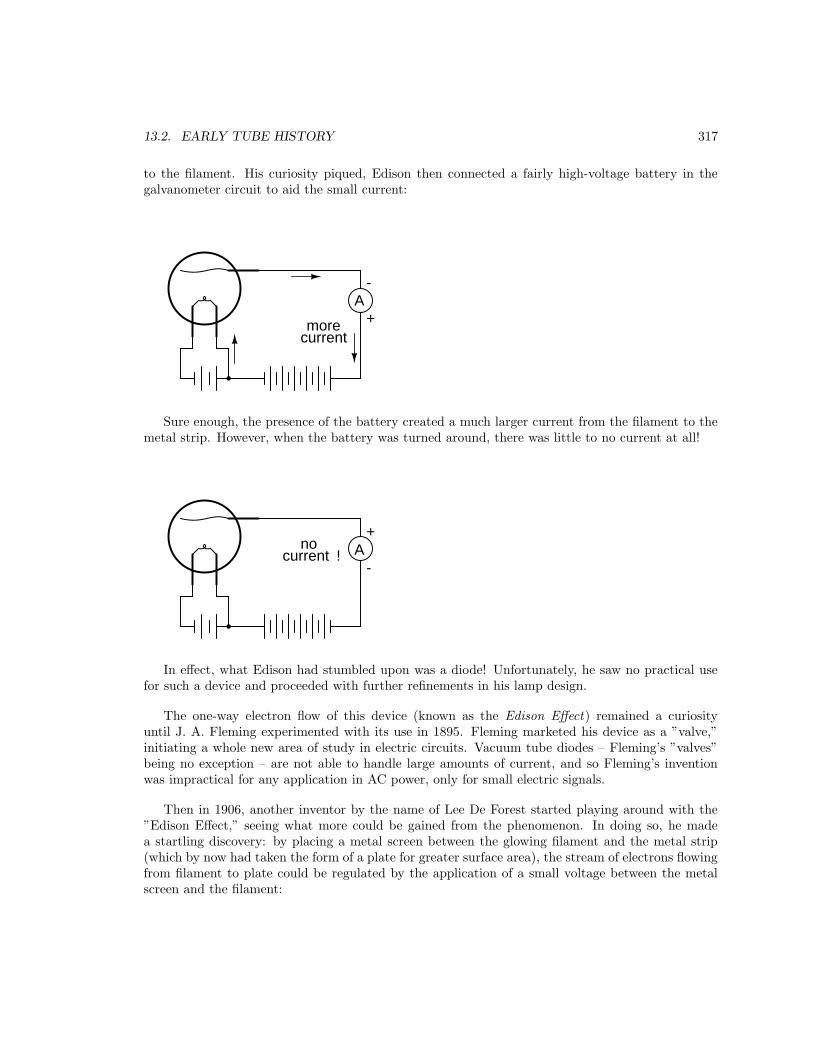
13.2. EARLY TUBE HISTORY 317
to the filament. His curiosity piqued, Edison then connected a fairly high-voltage battery in thegalvanometer circuit to aid the small current:
+A
-
morecurrent
Sure enough, the presence of the battery created a much larger current from the filament to themetal strip. However, when the battery was turned around, there was little to no current at all!
+A
-current
no!
In effect, what Edison had stumbled upon was a diode! Unfortunately, he saw no practical usefor such a device and proceeded with further refinements in his lamp design.
The one-way electron flow of this device (known as the Edison Effect) remained a curiosityuntil J. A. Fleming experimented with its use in 1895. Fleming marketed his device as a ”valve,”initiating a whole new area of study in electric circuits. Vacuum tube diodes – Fleming’s ”valves”being no exception – are not able to handle large amounts of current, and so Fleming’s inventionwas impractical for any application in AC power, only for small electric signals.
Then in 1906, another inventor by the name of Lee De Forest started playing around with the”Edison Effect,” seeing what more could be gained from the phenomenon. In doing so, he madea startling discovery: by placing a metal screen between the glowing filament and the metal strip(which by now had taken the form of a plate for greater surface area), the stream of electrons flowingfrom filament to plate could be regulated by the application of a small voltage between the metalscreen and the filament:
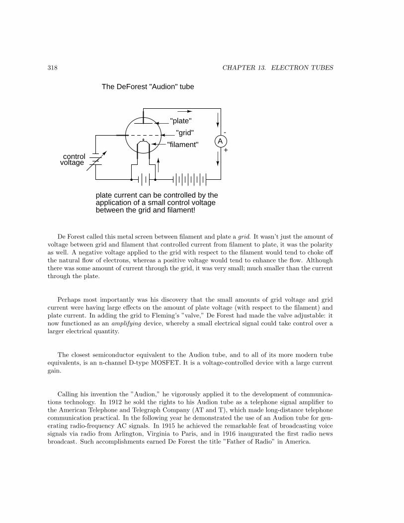
318 CHAPTER 13. ELECTRON TUBES
+A
-
controlvoltage
"plate"
"grid"
"filament"
plate current can be controlled by theapplication of a small control voltagebetween the grid and filament!
The DeForest "Audion" tube
De Forest called this metal screen between filament and plate a grid. It wasn’t just the amount ofvoltage between grid and filament that controlled current from filament to plate, it was the polarityas well. A negative voltage applied to the grid with respect to the filament would tend to choke offthe natural flow of electrons, whereas a positive voltage would tend to enhance the flow. Althoughthere was some amount of current through the grid, it was very small; much smaller than the currentthrough the plate.
Perhaps most importantly was his discovery that the small amounts of grid voltage and gridcurrent were having large effects on the amount of plate voltage (with respect to the filament) andplate current. In adding the grid to Fleming’s ”valve,” De Forest had made the valve adjustable: itnow functioned as an amplifying device, whereby a small electrical signal could take control over alarger electrical quantity.
The closest semiconductor equivalent to the Audion tube, and to all of its more modern tubeequivalents, is an n-channel D-type MOSFET. It is a voltage-controlled device with a large currentgain.
Calling his invention the ”Audion,” he vigorously applied it to the development of communica-tions technology. In 1912 he sold the rights to his Audion tube as a telephone signal amplifier tothe American Telephone and Telegraph Company (AT and T), which made long-distance telephonecommunication practical. In the following year he demonstrated the use of an Audion tube for gen-erating radio-frequency AC signals. In 1915 he achieved the remarkable feat of broadcasting voicesignals via radio from Arlington, Virginia to Paris, and in 1916 inaugurated the first radio newsbroadcast. Such accomplishments earned De Forest the title ”Father of Radio” in America.

13.3. THE TRIODE 319
13.3 The triode
De Forest’s Audion tube came to be known as the triode tube, because it had three elements:filament, grid, and plate (just as the ”di” in the name diode refers to two elements, filament andplate). Later developments in diode tube technology led to the refinement of the electron emitter:instead of using the filament directly as the emissive element, another metal strip called the cathodecould be heated by the filament.This refinement was necessary in order to avoid some undesired effects of an incandescent filament
as an electron emitter. First, a filament experiences a voltage drop along its length, as currentovercomes the resistance of the filament material and dissipates heat energy. This meant that thevoltage potential between different points along the length of the filament wire and other elementsin the tube would not be constant. For this and similar reasons, alternating current used as a powersource for heating the filament wire would tend to introduce unwanted AC ”noise” in the rest ofthe tube circuit. Furthermore, the surface area of a thin filament was limited at best, and limitedsurface area on the electron emitting element tends to place a corresponding limit on the tube’scurrent-carrying capacity.The cathode was a thin metal cylinder fitting snugly over the twisted wire of the filament. The
cathode cylinder would be heated by the filament wire enough to freely emit electrons, without theundesirable side effects of actually carrying the heating current as the filament wire had to. Thetube symbol for a triode with an indirectly-heated cathode looks like this:
plate
grid
cathode filament
Since the filament is necessary for all but a few types of vacuum tubes, it is often omitted in the

320 CHAPTER 13. ELECTRON TUBES
symbol for simplicity, or it may be included in the drawing but with no power connections drawn toit:
...
...
...
to filament wiresno connections shownno filament
shown at all
A simple triode circuit is shown to illustrate its basic operation as an amplifier:
R
voltageoutput
inputvoltage
DC powersource
"plate supply"
Triode amplifier circuit
The low-voltage AC signal connected between the grid and cathode alternately suppresses, thenenhances the electron flow between cathode and plate. This causes a change in voltage on theoutput of the circuit (between plate and cathode). The AC voltage and current magnitudes on thetube’s grid are generally quite small compared with the variation of voltage and current in the platecircuit. Thus, the triode functions as an amplifier of the incoming AC signal (taking high-voltage,high-current DC power supplied from the large DC source on the right and ”throttling” it by meansof the tube’s controlled conductivity).In the triode, the amount of current from cathode to plate (the ”controlled” current is a func-
tion both of grid-to-cathode voltage (the controlling signal) and the plate-to-cathode voltage (theelectromotive force available to push electrons through the vacuum). Unfortunately, neither of theseindependent variables have a purely linear effect on the amount of current through the device (oftenreferred to simply as the ”plate current”). That is, triode current does not necessarily respond in adirect, proportional manner to the voltages applied.In this particular amplifier circuit the nonlinearities are compounded, as plate voltage (with
respect to cathode) changes along with the grid voltage (also with respect to cathode) as plate

13.4. THE TETRODE 321
current is throttled by the tube. The result will be an output voltage waveform that doesn’t preciselyresemble the waveform of the input voltage. In other words, the quirkiness of the triode tube andthe dynamics of this particular circuit will distort the waveshape. If we really wanted to get complexabout how we stated this, we could say that the tube introduces harmonics by failing to exactlyreproduce the input waveform.
Another problem with triode behavior is that of stray capacitance. Remember that any time wehave two conductive surfaces separated by an insulating medium, a capacitor will be formed. Anyvoltage between those two conductive surfaces will generate an electric field within that insulatingregion, potentially storing energy and introducing reactance into a circuit. Such is the case with thetriode, most problematically between the grid and the plate. It is as if there were tiny capacitorsconnected between the pairs of elements in the tube:
Cgrid-plate
Cgrid-cathode
Cplate-cathode
Now, this stray capacitance is quite small, and the reactive impedances usually high. Usually,that is, unless radio frequencies are being dealt with. As we saw with De Forest’s Audion tube,radio was probably the prime application for this new technology, so these ”tiny” capacitancesbecame more than just a potential problem. Another refinement in tube technology was necessaryto overcome the limitations of the triode.
13.4 The tetrode
As the name suggests, the tetrode tube contained four elements: cathode (with the implicit filament,or ”heater”), grid, plate, and a new element called the screen. Similar in construction to the grid, thescreen was a wire mesh or coil positioned between the grid and plate, connected to a source of positiveDC potential (with respect to the cathode, as usual) equal to a fraction of the plate voltage. Whenconnected to ground through an external capacitor, the screen had the effect of electrostaticallyshielding the grid from the plate. Without the screen, the capacitive linking between the plate andthe grid could cause significant signal feedback at high frequencies, resulting in unwanted oscillations.
The screen, being of less surface area and lower positive potential than the plate, didn’t attractmany of the electrons passing through the grid from the cathode, so the vast majority of electronsin the tube still flew by the screen to be collected by the plate:

322 CHAPTER 13. ELECTRON TUBES
R
inputvoltage
DC powersource
"plate supply""screen"
R
R C
Tetrode amplifier circuit
With a constant DC screen voltage, electron flow from cathode to plate became almost exclusivelydependent upon grid voltage, meaning the plate voltage could vary over a wide range with little effecton plate current. This made for more stable gains in amplifier circuits, and better linearity for moreaccurate reproduction of the input signal waveform.Despite the advantages realized by the addition of a screen, there were some disadvantages as
well. The most significant disadvantage was related to something known as secondary emission.When electrons from the cathode strike the plate at high velocity, they can cause free electrons tobe jarred loose from atoms in the metal of the plate. These electrons, knocked off the plate by theimpact of the cathode electrons, are said to be ”secondarily emitted.” In a triode tube, secondaryemission is not that great a problem, but in a tetrode with a positively-charged screen grid in closeproximity, these secondary electrons will be attracted to the screen rather than the plate from whichthey came, resulting in a loss of plate current. Less plate current means less gain for the amplifier,which is not good.Two different strategies were developed to address this problem of the tetrode tube: beam power
tubes and pentodes. Both solutions resulted in new tube designs with approximately the sameelectrical characteristics.
13.5 Beam power tubes
In the beam power tube, the basic four-element structure of the tetrode was maintained, but the gridand screen wires were carefully arranged along with a pair of auxiliary plates to create an interestingeffect: focused beams or ”sheets” of electrons traveling from cathode to plate. These electron beamsformed a stationary ”cloud” of electrons between the screen and plate (called a ”space charge”)which acted to repel secondary electrons emitted from the plate back to the plate. A set of ”beam-forming” plates, each connected to the cathode, were added to help maintain proper electron beamfocus. Grid and screen wire coils were arranged in such a way that each turn or wrap of the screenfell directly behind a wrap of the grid, which placed the screen wires in the ”shadow” formed by thegrid. This precise alignment enabled the screen to still perform its shielding function with minimalinterference to the passage of electrons from cathode to plate.

13.6. THE PENTODE 323
platecathode
grid wires(cross-sectional view)
(cross-sectional view)screen wires
beam-forming plates(2)
electron beams
-
-- --------- -
-------------- ---- -
- -
--
---
----
-
"space charge"
This resulted in lower screen current (and more plate current!) than an ordinary tetrode tube,with little added expense to the construction of the tube.
Beam power tetrodes were often distinguished from their non-beam counterparts by a differentschematic symbol, showing the beam-forming plates:
cathode
plate
screengrid
The "Beam power" tetrode tube
13.6 The pentode
Another strategy for addressing the problem of secondary electrons being attracted by the screenwas the addition of a fifth wire element to the tube structure: a suppressor. These five-elementtubes were naturally called pentodes.

324 CHAPTER 13. ELECTRON TUBES
cathode
grid
plate
screensuppressor
The pentode tube
The suppressor was another wire coil or mesh situated between the screen and the plate, usuallyconnected directly to ground potential. In some pentode tube designs, the suppressor was internallyconnected to the cathode so as to minimize the number of connection pins having to penetrate thetube envelope:
cathode
grid
plate
screen
(suppressor internallyconnected to cathode)
The suppressor’s job was to repel any secondarily emitted electrons back to the plate: a structuralequivalent of the beam power tube’s space charge. This, of course, increased plate current anddecreased screen current, resulting in better gain and overall performance. In some instances itallowed for greater operating plate voltage as well.
13.7 Combination tubes
Similar in thought to the idea of the integrated circuit, tube designers tried integrating differenttube functions into single tube envelopes to reduce space requirements in more modern tube-typeelectronic equipment. A common combination seen within a single glass shell was two either diodesor two triodes. The idea of fitting pairs of diodes inside a single envelope makes a lot of sense inlight of power supply full-wave rectifier designs, always requiring multiple diodes.Of course, it would have been quite impossible to combine thousands of tube elements into a
single tube envelope the way that thousands of transistors can be etched onto a single piece of silicon,but engineers still did their best to push the limits of tube miniaturization and consolidation. Someof these tubes, whimsically called compactrons, held four or more complete tube elements within asingle envelope.Sometimes the functions of two different tubes could be integrated into a single, combination
tube in a way that simply worked more elegantly than two tubes ever could. An example of thiswas the pentagrid converter, more generally called a heptode, used in some superheterodyne radiodesigns. These tubes contained seven elements: 5 grids plus a cathode and a plate. Two of the

13.7. COMBINATION TUBES 325
grids were normally reserved for signal input, the other three relegated to screening and suppression(performance-enhancing) functions. Combining the superheterodyne functions of oscillator and sig-nal mixer together in one tube, the signal coupling between these two stages was intrinsic. Ratherthan having separate oscillator and mixer circuits, the oscillator creating an AC voltage and themixer ”mixing” that voltage with another signal, the pentagrid converter’s oscillator section createdan electron stream that oscillated in intensity which then directly passed through another grid for”mixing” with another signal.
This same tube was sometimes used in a different way: by applying a DC voltage to one of thecontrol grids, the gain of the tube could be changed for a signal impressed on the other controlgrid. This was known as variable-mu operation, because the ”mu” (µ) of the tube (its amplificationfactor, measured as a ratio of plate-to-cathode voltage change over grid-to-cathode voltage changewith a constant plate current) could be altered at will by a DC control voltage signal.
Enterprising electronics engineers also discovered ways to exploit such multi-variable capabilitiesof ”lesser” tubes such as tetrodes and pentodes. One such way was the so-called ultralinear audiopower amplifier, invented by a pair of engineers named Hafler and Keroes, utilizing a tetrode tube incombination with a ”tapped” output transformer to provide substantial improvements in amplifierlinearity (decreases in distortion levels). Consider a ”single-ended” triode tube amplifier with anoutput transformer coupling power to the speaker:
inputvoltage
Speaker
If we substitute a tetrode for a triode in this circuit, we will see improvements in circuit gain re-sulting from the electrostatic shielding offered by the screen, preventing unwanted feedback betweenthe plate and control grid:

326 CHAPTER 13. ELECTRON TUBES
inputvoltage
SpeakerStandard configuration
of tetrode tubein a single-endedaudio amplifier
However, the tetrode’s screen may be used for functions other than merely shielding the gridfrom the plate. It can also be used as another control element, like the grid itself. If a ”tap” is madeon the transformer’s primary winding, and this tap connected to the screen, the screen will receivea voltage that varies with the signal being amplified (feedback). More specifically, the feedbacksignal is proportional to the rate-of-change of magnetic flux in the transformer core (dΦ/dt), thusimproving the amplifier’s ability to reproduce the input signal waveform at the speaker terminalsand not just in the primary winding of the transformer:
inputvoltage
Speakerconfiguration
of tetrode tubein a single-endedaudio amplifier
"Ultralinear"
This signal feedback results in significant improvements in amplifier linearity (and consequently,distortion), so long as precautions are taken against ”overpowering” the screen with too great a

13.8. TUBE PARAMETERS 327
positive voltage with respect to the cathode. As a concept, the ultralinear (screen-feedback) designdemonstrates the flexibility of operation granted by multiple grid-elements inside a single tube: acapability rarely matched by semiconductor components.
Some tube designs combined multiple tube functions in a most economic way: dual plates witha single cathode, the currents for each of the plates controlled by separate sets of control grids.Common examples of these tubes were triode-heptode and triode-hexode tubes (a hexode tube is atube with four grids, one cathode, and one plate).
Other tube designs simply incorporated separate tube structures inside a single glass envelopefor greater economy. Dual diode (rectifier) tubes were quite common, as were dual triode tubes,especially when the power dissipation of each tube was relatively low.
Dual triode tube
The 12AX7 and 12AU7 models are common examples of dual-triode tubes, both of low-powerrating. The 12AX7 is especially common as a preamplifier tube in electric guitar amplifier circuits.
13.8 Tube parameters
For bipolar junction transistors, the fundamental measure of amplification is the Beta ratio (β),defined as the ratio of collector current to base current (IC/IB). Other transistor characteristicssuch as junction resistance, which in some amplifier circuits may impact performance as much as β,are quantified for the benefit of circuit analysis. Electron tubes are no different, their performancecharacteristics having been explored and quantified long ago by electrical engineers.
Before we can speak meaningfully on these characteristics, we must define several mathematicalvariables used for expressing common voltage, current, and resistance measurements as well as someof the more complex quantities:

328 CHAPTER 13. ELECTRON TUBES
µ = amplification factor, pronounced "mu"
gm = mutual conductance, in siemens(unitless)
Eg = grid-to-cathode voltage
Ip = plate current
Ep = plate-to-cathode voltage
Ik = cathode current
Es = input signal voltage
rp = dynamic plate resistance, in ohms
∆ = delta, the Greek symbol for change
The two most basic measures of an amplifying tube’s characteristics are its amplification factor(µ) and its mutual conductance (gm), also known as transconductance. Transconductance is definedhere just the same as it is for field-effect transistors, another category of voltage-controlled devices.Here are the two equations defining each of these performance characteristics:
µ =∆Ep
∆Eg
with constant Ip (plate current)
gm = ∆Ip
∆Eg
with constant Ep (plate voltage)
Another important, though more abstract, measure of tube performance is its plate resistance.This is the measurement of plate voltage change over plate current change for a constant value ofgrid voltage. In other words, this is an expression of how much the tube acts like a resistor for anygiven amount of grid voltage, analogous to the operation of a JFET in its ohmic mode:
∆Eprp = ∆Ip
with constant Eg (grid voltage)
The astute reader will notice that plate resistance may be determined by dividing the amplifica-tion factor by the transconductance:

13.9. IONIZATION (GAS-FILLED) TUBES 329
∆Eprp = ∆Ip
µ = ∆Ep
∆Eg
gm = ∆Eg
∆Ip
. . . dividing µ by gm . . .
∆Ep
∆Eg
∆Ip
∆Eg
rp =
rp =∆Ep
∆Eg
∆Eg
∆Ip
These three performance measures of tubes are subject to change from tube to tube (just as βratios between two ”identical” bipolar transistors are never precisely the same) and between differentoperating conditions. This variability is due partly to the unavoidable nonlinearities of electron tubesand partly due to how they are defined. Even supposing the existence of a perfectly linear tube,it will be impossible for all three of these measures to be constant over the allowable ranges ofoperation. Consider a tube that perfectly regulates current at any given amount of grid voltage (likea bipolar transistor with an absolutely constant β): that tube’s plate resistance must vary withplate voltage, because plate current will not change even though plate voltage does.Nevertheless, tubes were (and are) rated by these values at given operating conditions, and may
have their characteristic curves published just like transistors.
13.9 Ionization (gas-filled) tubes
So far, we’ve explored tubes which are totally ”evacuated” of all gas and vapor inside their glassenvelopes, properly known as vacuum tubes. With the addition of certain gases or vapors, however,tubes take on significantly different characteristics, and are able to fulfill certain special roles inelectronic circuits.When a high enough voltage is applied across a distance occupied by a gas or vapor, or when
that gas or vapor is heated sufficiently, the electrons of those gas molecules will be stripped awayfrom their respective nuclei, creating a condition of ionization. Having freed the electrons from theirelectrostatic bonds to the atoms’ nuclei, they are free to migrate in the form of a current, makingthe ionized gas a relatively good conductor of electricity. In this state, the gas is more properlyreferred to as a plasma.Ionized gas is not a perfect conductor. As such, the flow of electrons through ionized gas will
tend to dissipate energy in the form of heat, thereby helping to keep the gas in a state of ionization.The result of this is a tube that will begin to conduct under certain conditions, then tend to stay

330 CHAPTER 13. ELECTRON TUBES
in a state of conduction until the applied voltage across the gas and/or the heat-generating currentdrops to a minimum level.
The astute observer will note that this is precisely the kind of behavior exhibited by a class ofsemiconductor devices called ”thyristors,” which tend to stay ”on” once turned ”on” and tend to stay”off” once turned ”off.” Gas-filled tubes, it can be said, manifest this same property of hysteresis.
Unlike their vacuum counterparts, ionization tubes were often manufactured with no filament(heater) at all. These were called cold-cathode tubes, with the heated versions designated as hot-cathode tubes. Whether or not the tube contained a source of heat obviously impacted the charac-teristics of a gas-filled tube, but not to the extent that lack of heat would impact the performanceof a hard-vacuum tube.
The simplest type of ionization device is not necessarily a tube at all; rather, it is constructedof two electrodes separated by a gas-filled gap. Simply called a spark gap, the gap between theelectrodes may be occupied by ambient air, other times a special gas, in which case the device musthave a sealed envelope of some kind.
electrodes
enclosure (optional)Spark gap
A prime application for spark gaps is in overvoltage protection. Engineered not to ionize, or”break down” (begin conducting), with normal system voltage applied across the electrodes, thespark gap’s function is to conduct in the event of a significant increase in voltage. Once conducting,it will act as a heavy load, holding the system voltage down through its large current draw andsubsequent voltage drop along conductors and other series impedances. In a properly engineeredsystem, the spark gap will stop conducting (”extinguish”) when the system voltage decreases to anormal level, well below the voltage required to initiate conduction.
One major caveat of spark gaps is their significantly finite life. The discharge generated by sucha device can be quite violent, and as such will tend to deteriorate the surfaces of the electrodesthrough pitting and/or melting.
Spark gaps can be made to conduct on command by placing a third electrode (usually with asharp edge or point) between the other two and applying a high voltage pulse between that electrodeand one of the other electrodes. The pulse will create a small spark between the two electrodes,ionizing part of the pathway between the two large electrodes, and enabling conduction betweenthem if the applied voltage is high enough:

13.9. IONIZATION (GAS-FILLED) TUBES 331
third electrode
Load
triggering voltage
mainvoltagesource
source(high voltage, low current)
(high voltage,high current)
spark gap
Triggered spark gap
Spark gaps of both the triggered and untriggered variety can be built to handle huge amountsof current, some even into the range of mega-amps (millions of amps)! Physical size is the primarylimiting factor to the amount of current a spark gap can safely and reliably handle.
When the two main electrodes are placed in a sealed tube filled with a special gas, a dischargetube is formed. The most common type of discharge tube is the neon light, used popularly as asource of colorful illumination, the color of the light emitted being dependent on the type of gasfilling the tube.
Construction of neon lamps closely resembles that of spark gaps, but the operational character-istics are quite different:

332 CHAPTER 13. ELECTRON TUBES
electrode electrode
glass tube
current through the tubecauses the neon gas to glow
NEON LAMP
high voltage power supply (AC or DC)
small neonindicator lamp
Neon lamp schematic symbol
By controlling the spacing of the electrodes and the type of gas in the tube, neon lights canbe made to conduct without drawing the excessive currents that spark gaps do. They still exhibithysteresis in that it takes a higher voltage to initiate conduction than it does to make them ”ex-tinguish,” and their resistance is definitely nonlinear (the more voltage applied across the tube, themore current, thus more heat, thus lower resistance). Given this nonlinear tendency, the voltageacross a neon tube must not be allowed to exceed a certain limit, lest the tube be damaged byexcessive temperatures.
This nonlinear tendency gives the neon tube an application other than colorful illumination: itcan act somewhat like a zener diode, ”clamping” the voltage across it by drawing more and morecurrent if the voltage decreases. When used in this fashion, the tube is known as a glow tube, orvoltage-regulator tube, and was a popular means of voltage regulation in the days of electron tubecircuit design.
Rload
Rseries
glow-dischargevoltage regulator
tube
voltage across loadheld relative constant
with variations of voltagesource and load resistance
Please take note of the black dot found in the tube symbol shown above (and in the neon lampsymbol shown before that). That marker indicates the tube is gas-filled. It is a common markerused in all gas-filled tube symbols.
One example of a glow tube designed for voltage regulation was the VR-150, with a nominalregulating voltage of 150 volts. Its resistance throughout the allowable limits of current could vary

13.10. DISPLAY TUBES 333
from 5 kΩ to 30 kΩ, a 6:1 span. Like zener diode regulator circuits of today, glow tube regulatorscould be coupled to amplifying tubes for better voltage regulation and higher load current ranges.
If a regular triode was filled with gas instead of a hard vacuum, it would manifest all thehysteresis and nonlinearity of other gas tubes with one major advantage: the amount of voltageapplied between grid and cathode would determine the minimum plate-to cathode voltage necessaryto initiate conduction. In essence, this tube was the equivalent of the semiconductor SCR (Silicon-Controlled Rectifier), and was called the thyratron.
Rload
controlvoltage
ThyratronTube high voltage
AC source
+
-
(Simple) Thyratron control circuit
It should be noted that the schematic shown above is greatly simplified for most purposes andthyratron tube designs. Some thyratrons, for instance, required that the grid voltage switch polaritybetween their ”on” and ”off” states in order to properly work. Also, some thyratrons had more thanone grid!
Thyratrons found use in much the same way as SCR’s find use today: controlling rectified ACto large loads such as motors. Thyratron tubes have been manufactured with different types of gasfillings for different characteristics: inert (chemically non-reactive) gas, hydrogen gas, and mercury(vaporized into a gas form when activated). Deuterium, a rare isotope of hydrogen, was used insome special applications requiring the switching of high voltages.
13.10 Display tubes
In addition to performing tasks of amplification and switching, tubes can be designed to serve asdisplay devices.
Perhaps the best-known display tube is the cathode ray tube, or CRT. Originally invented as aninstrument to study the behavior of ”cathode rays” (electrons) in a vacuum, these tubes developedinto instruments useful in detecting voltage, then later as video projection devices with the adventof television. The main difference between CRTs used in oscilloscopes and CRTs used in televisionsis that the oscilloscope variety exclusively use electrostatic (plate) deflection, while televisions useelectromagnetic (coil) deflection. Plates function much better than coils over a wider range of signalfrequencies, which is great for oscilloscopes but irrelevant for televisions, since a television electronbeam sweeps vertically and horizontally at fixed frequencies. Electromagnetic deflection coils aremuch preferred in television CRT construction because they do not have to penetrate the glass

334 CHAPTER 13. ELECTRON TUBES
envelope of the tube, thus decreasing the production costs and increasing tube reliability.
An interesting ”cousin” to the CRT is the Cat-Eye or Magic-Eye indicator tube. Essentially,this tube is a voltage-measuring device with a display resembling a glowing green ring. Electronsemitted by the cathode of this tube impinge on a fluorescent screen, causing the green-colored lightto be emitted. The shape of the glow produced by the fluorescent screen varies as the amount ofvoltage applied to a grid changes:
minimal shadowslight shadowlarge shadow
"Cat-Eye" indicator tube displays
The width of the shadow is directly determined by the potential difference between the controlelectrode and the fluorescent screen. The control electrode is a narrow rod placed between thecathode and the fluorescent screen. If that control electrode (rod) is significantly more negativethan the fluorescent screen, it will deflect some electrons away from the that area of the screen. Thearea of the screen ”shadowed” by the control electrode will appear darker when there is a significantvoltage difference between the two. When the control electrode and fluorescent screen are at equalpotential (zero voltage between them), the shadowing effect will be minimal and the screen will beequally illuminated.
The schematic symbol for a ”cat-eye” tube looks something like this:
screenplatecontrol
amplifiergrid
cathode
electrode
fluorescent
"Cat-Eye" or "Magic-Eye"indicator tube
Here is a photograph of a cat-eye tube, showing the circular display region as well as the glassenvelope, socket (black, at far end of tube), and some of its internal structure:

13.10. DISPLAY TUBES 335
Normally, only the end of the tube would protrude from a hole in an instrument panel, so theuser could view the circular, fluorescent screen.
In its simplest usage, a ”cat-eye” tube could be operated without the use of the amplifier grid.However, in order to make it more sensitive, the amplifier grid is used, and it is used like this:
R
signal
As the signal voltage increases, current through
"Cat-Eye" indicator tube circuit
the tube is choked off. This decreases the voltage
lessening the shadow effect (shadow narrows). between the plate and the fluorescent screen,
The cathode, amplifier grid, and plate act as a triode to create large changes in plate-to-cathodevoltage for small changes in grid-to-cathode voltage. Because the control electrode is internallyconnected to the plate, it is electrically common to it and therefore possesses the same amount ofvoltage with respect to the cathode that the plate does. Thus, the large voltage changes inducedon the plate due to small voltage changes on the amplifier grid end up causing large changes in thewidth of the shadow seen by whoever is viewing the tube.

336 CHAPTER 13. ELECTRON TUBES
Control electrode negative with
This is caused by a positive amplifier grid voltage (with respect to the cathode).
This is caused by a negativeamplifier grid voltage (with respect to the cathode).
respect to the fluorescent screen.No voltage between controlelectrode and flourescent screen.
”Cat-eye” tubes were never accurate enough to be equipped with a graduated scale as is the casewith CRT’s and electromechanical meter movements, but they served well as null detectors in bridgecircuits, and as signal strength indicators in radio tuning circuits. An unfortunate limitation to the”cat-eye” tube as a null detector was the fact that it was not directly capable of voltage indicationin both polarities.
13.11 Microwave tubes
For extremely high-frequency applications (above 1 GHz), the interelectrode capacitances and transit-time delays of standard electron tube construction become prohibitive. However, there seems to beno end to the creative ways in which tubes may be constructed, and several high-frequency electrontube designs have been made to overcome these challenges.It was discovered in 1939 that a toroidal cavity made of conductive material called a cavity
resonator surrounding an electron beam of oscillating intensity could extract power from the beamwithout actually intercepting the beam itself. The oscillating electric and magnetic fields associatedwith the beam ”echoed” inside the cavity, in a manner similar to the sounds of traveling automobilesechoing in a roadside canyon, allowing radio-frequency energy to be transferred from the beam to awaveguide or coaxial cable connected to the resonator with a coupling loop. The tube was called aninductive output tube, or IOT :
DC supply
RFsignalinput
toroidal cavity
coaxialoutputcable
electron beam
RF power output
The inductive output tube (IOT)
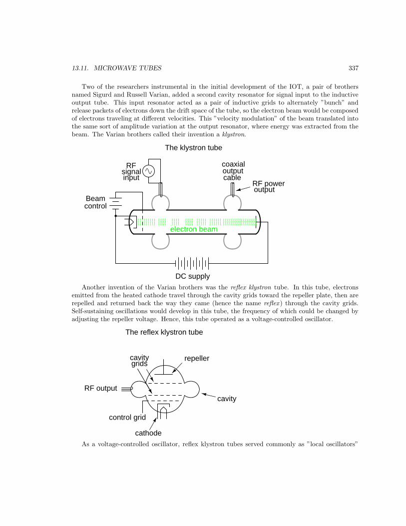
13.11. MICROWAVE TUBES 337
Two of the researchers instrumental in the initial development of the IOT, a pair of brothersnamed Sigurd and Russell Varian, added a second cavity resonator for signal input to the inductiveoutput tube. This input resonator acted as a pair of inductive grids to alternately ”bunch” andrelease packets of electrons down the drift space of the tube, so the electron beam would be composedof electrons traveling at different velocities. This ”velocity modulation” of the beam translated intothe same sort of amplitude variation at the output resonator, where energy was extracted from thebeam. The Varian brothers called their invention a klystron.
DC supply
RFsignalinput
coaxialoutputcable
electron beam
RF power output
The klystron tube
Beamcontrol
Another invention of the Varian brothers was the reflex klystron tube. In this tube, electronsemitted from the heated cathode travel through the cavity grids toward the repeller plate, then arerepelled and returned back the way they came (hence the name reflex ) through the cavity grids.Self-sustaining oscillations would develop in this tube, the frequency of which could be changed byadjusting the repeller voltage. Hence, this tube operated as a voltage-controlled oscillator.
repeller
RF outputcavity
cathode
cavitygrids
control grid
The reflex klystron tube
As a voltage-controlled oscillator, reflex klystron tubes served commonly as ”local oscillators”

338 CHAPTER 13. ELECTRON TUBES
for radar equipment and microwave receivers:
Reflex klystron tube used asa voltage-controlled oscillator
Initially developed as low-power devices whose output required further amplification for radiotransmitter use, reflex klystron design was refined to the point where the tubes could serve as powerdevices in their own right. Reflex klystrons have since been superseded by semiconductor devices inthe application of local oscillators, but amplification klystrons continue to find use in high-power,high-frequency radio transmitters and in scientific research applications.
One microwave tube performs its task so well and so cost-effectively that it continues to reignsupreme in the competitive realm of consumer electronics: the magnetron tube. This device formsthe heart of every microwave oven, generating several hundred watts of microwave RF energy usedto heat food and beverages, and doing so under the most grueling conditions for a tube: poweredon and off at random times and for random durations.
Magnetron tubes are representative of an entirely different kind of tube than the IOT andklystron. Whereas the latter tubes use a linear electron beam, the magnetron directs its electronbeam in a circular pattern by means of a strong magnetic field:

13.12. TUBES VERSUS SEMICONDUCTORS 339
cathode
electron
beam
cavityresonators
RF output
The magnetron tube
Once again, cavity resonators are used as microwave-frequency ”tank circuits,” extracting energyfrom the passing electron beam inductively. Like all microwave-frequency devices using a cavityresonator, at least one of the resonator cavities is tapped with a coupling loop: a loop of wiremagnetically coupling the coaxial cable to the resonant structure of the cavity, allowing RF powerto be directed out of the tube to a load. In the case of the microwave oven, the output power isdirected through a waveguide to the food or drink to be heated, the water molecules within actingas tiny load resistors, dissipating the electrical energy in the form of heat.
The magnet required for magnetron operation is not shown in the diagram. Magnetic flux runsperpendicular to the plane of the circular electron path. In other words, from the view of the tubeshown in the diagram, you are looking straight at one of the magnetic poles.
13.12 Tubes versus Semiconductors
Devoting a whole chapter in a modern electronics text to the design and function of electron tubesmay seem a bit strange, seeing as how semiconductor technology has all but obsoleted tubes in almostevery application. However, there is merit in exploring tubes not just for historical purposes, butalso for those niche applications that necessitate the qualifying phrase ”almost every application”in regard to semiconductor supremacy.
In some applications, electron tubes not only continue to see practical use, but perform theirrespective tasks better than any solid-state device yet invented. In some cases the performance andreliability of electron tube technology is far superior.
In the fields of high-power, high-speed circuit switching, specialized tubes such as hydrogenthyratrons and krytrons are able to switch far larger amounts of current, far faster than any semi-conductor device designed to date. The thermal and temporal limits of semiconductor physics placelimitations on switching ability that tubes – which do not operate on the same principles – areexempt from.
In high-power microwave transmitter applications, the excellent thermal tolerance of tubes alonesecures their dominance over semiconductors. Electron conduction through semiconducting ma-terials is greatly impacted by temperature. Electron conduction through a vacuum is not. As a

340 CHAPTER 13. ELECTRON TUBES
consequence, the practical thermal limits of semiconductor devices are rather low compared to thatof tubes. Being able to operate tubes at far greater temperatures than equivalent semiconductordevices allows tubes to dissipate more thermal energy for a given amount of dissipation area, whichmakes them smaller and lighter in continuous high power applications.
Another decided advantage of tubes over semiconductor components in high-power applicationsis their rebuildability. When a large tube fails, it may be disassembled and repaired at far lowercost than the purchase price of a new tube. When a semiconductor component fails, large or small,there is generally no means of repair.
The following photograph shows the front panel of a 1960’s vintage 5 kW AM radio transmitter.One of two ”Eimac” brand power tubes can be seen in a recessed area, behind the glass door.According to the station engineer who gave the facility tour, the rebuild cost for such a tube is only$800: quite inexpensive compared to the cost of a new tube, and still quite reasonable in contrastto the price of a new, comparable semiconductor component!
Tubes, being less complex in their manufacture than semiconductor components, are potentiallycheaper to produce as well, although the huge volume of semiconductor device production in theworld greatly offsets this theoretical advantage. Semiconductor manufacture is quite complex, in-volving many dangerous chemical substances and necessitating super-clean assembly environments.Tubes are essentially nothing more than glass and metal, with a vacuum seal. Physical tolerancesare ”loose” enough to permit hand-assembly of vacuum tubes, and the assembly work need not bedone in a ”clean room” environment as is necessary for semiconductor manufacture.
One modern area where electron tubes enjoy supremacy over semiconductor components is inthe professional and high-end audio amplifier markets, although this is partially due to musical cul-ture. Many professional guitar players, for example, prefer tube amplifiers over transistor amplifiersbecause of the specific distortion produced by tube circuits. An electric guitar amplifier is designedto produce distortion rather than avoid distortion as is the case with audio-reproduction amplifiers(this is why an electric guitar sounds so much different than an acoustical guitar), and the type ofdistortion produced by an amplifier is as much a matter of personal taste as it is technical mea-surement. Since rock music in particular was born with guitarists playing tube-amplifier equipment,there is a significant level of ”tube appeal” inherent to the genre itself, and this appeal shows itselfin the continuing demand for ”tubed” guitar amplifiers among rock guitarists.
As an illustration of the attitude among some guitarists, consider the following quote taken fromthe technical glossary page of a tube-amplifier website which will remain nameless:

13.12. TUBES VERSUS SEMICONDUCTORS 341
Solid State: A component that has been specifically designed to make a guitar am-plifier sound bad. Compared to tubes, these devices can have a very long lifespan, whichguarantees that your amplifier will retain its thin, lifeless, and buzzy sound for a longtime to come.
In the area of audio reproduction amplifiers (music studio amplifiers and home entertainmentamplifiers), it is best for an amplifier to reproduce the musical signal with as little distortion aspossible. Paradoxically, in contrast to the guitar amplifier market where distortion is a designgoal, high-end audio is another area where tube amplifiers enjoy continuing consumer demand.Though one might suppose the objective, technical requirement of low distortion would eliminateany subjective bias on the part of audiophiles, one would be very wrong. The market for high-end”tubed” amplifier equipment is quite volatile, changing rapidly with trends and fads, driven byhighly subjective claims of ”magical” sound from audio system reviewers and salespeople. As in theelectric guitar world, there is no small measure of cult-like devotion to tube amplifiers among somequarters of the audiophile world. As an example of this irrationality, consider the design of manyultra-high-end amplifiers, with chassis built to display the working tubes openly, even though thisphysical exposure of the tubes obviously enhances the undesirable effect of microphonics (changesin tube performance as a result of sound waves vibrating the tube structure).Having said this, though, there is a wealth of technical literature contrasting tubes against
semiconductors for audio power amplifier use, especially in the area of distortion analysis. Morethan a few competent electrical engineers prefer tube amplifier designs over transistors, and are ableto produce experimental evidence in support of their choice. The primary difficulty in quantifyingaudio system performance is the uncertain response of human hearing. All amplifiers distort theirinput signal to some degree, especially when overloaded, so the question is which type of amplifierdesign distorts the least. However, since human hearing is very nonlinear, people do not interpretall types of acoustic distortion equally, and so some amplifiers will sound ”better” than others evenif a quantitative distortion analysis with electronic instruments indicates similar distortion levels.To determine what type of audio amplifier will distort a musical signal ”the least,” we must regardthe human ear and brain as part of the whole acoustical system. Since no complete model yet existsfor human auditory response, objective assessment is difficult at best. However, some researchindicates that the characteristic distortion of tube amplifier circuits (especially when overloaded) isless objectionable than distortion produced by transistors.Tubes also possess the distinct advantage of low ”drift” over a wide range of operating conditions.
Unlike semiconductor components, whose barrier voltages, β ratios, bulk resistances, and junctioncapacitances may change substantially with changes in device temperature and/or other operatingconditions, the fundamental characteristics of a vacuum tube remain nearly constant over a widerange in operating conditions, because those characteristics are determined primarily by the physicaldimensions of the tube’s structural elements (cathode, grid(s), and plate) rather than the interactionsof subatomic particles in a crystalline lattice.This is one of the major reasons solid-state amplifier designers typically engineer their circuits
to maximize power-efficiency even when it compromises distortion performance, because a power-inefficient amplifier dissipates a lot of energy in the form of waste heat, and transistor characteristicstend to change substantially with temperature. Temperature-induced ”drift” makes it difficult tostabilize ”Q” points and other important performance-related measures in an amplifier circuit. Un-fortunately, power efficiency and low distortion seem to be mutually exclusive design goals.For example, class A audio amplifier circuits typically exhibit very low distortion levels, but are

342 CHAPTER 13. ELECTRON TUBES
very wasteful of power, meaning that it would be difficult to engineer a solid-state class A amplifierof any substantial power rating due to the consequent drift of transistor characteristics. Thus, mostsolid-state audio amplifier designers choose class B circuit configurations for greater efficiency, eventhough class B designs are notorious for producing a type of distortion known as crossover distortion.However, with tubes it is easy to design a stable class A audio amplifier circuit because tubes arenot as adversely affected by the changes in temperature experienced in a such a power-inefficientcircuit configuration.Tube performance parameters, though, tend to ”drift” more than semiconductor devices when
measured over long periods of time (years). One major mechanism of tube ”aging” appears tobe vacuum leaks: when air enters the inside of a vacuum tube, its electrical characteristics becomeirreversibly altered. This same phenomenon is a major cause of tube mortality, or why tubes typicallydo not last as long as their respective solid-state counterparts. When tube vacuum is maintainedat a high level, though, excellent performance and life is possible. An example of this is a klystrontube (used to produce the high-frequency radio waves used in a radar system) that lasted for 240,000hours of operation (cited by Robert S. Symons of Litton Electron Devices Division in his informativepaper, ”Tubes: Still vital after all these years,” printed in the April 1998 issue of IEEE Spectrummagazine).If nothing else, the tension between audiophiles over tubes versus semiconductors has spurred
a remarkable degree of experimentation and technical innovation, serving as an excellent resourcefor those wishing to educate themselves on amplifier theory. Taking a wider view, the versatilityof electron tube technology (different physical configurations, multiple control grids) hints at thepotential for circuit designs of far greater variety than is possible using semiconductors. For thisand other reasons, electron tubes will never be ”obsolete,” but will continue to serve in niche roles,and to foster innovation for those electronics engineers, inventors, and hobbyists who are unwillingto let their minds by stifled by convention.

Appendix A-1
ABOUT THIS BOOK
A-1.1 Purpose
They say that necessity is the mother of invention. At least in the case of this book, that adageis true. As an industrial electronics instructor, I was forced to use a sub-standard textbook duringmy first year of teaching. My students were daily frustrated with the many typographical errorsand obscure explanations in this book, having spent much time at home struggling to comprehendthe material within. Worse yet were the many incorrect answers in the back of the book to selectedproblems. Adding insult to injury was the $100+ price.
Contacting the publisher proved to be an exercise in futility. Even though the particular text Iwas using had been in print and in popular use for a couple of years, they claimed my complaintwas the first they’d ever heard. My request to review the draft for the next edition of their bookwas met with disinterest on their part, and I resolved to find an alternative text.
Finding a suitable alternative was more difficult than I had imagined. Sure, there were plenty oftexts in print, but the really good books seemed a bit too heavy on the math and the less intimidatingbooks omitted a lot of information I felt was important. Some of the best books were out of print,and those that were still being printed were quite expensive.
It was out of frustration that I compiled Lessons in Electric Circuits from notes and ideas I hadbeen collecting for years. My primary goal was to put readable, high-quality information into thehands of my students, but a secondary goal was to make the book as affordable as possible. Over theyears, I had experienced the benefit of receiving free instruction and encouragement in my pursuitof learning electronics from many people, including several teachers of mine in elementary and highschool. Their selfless assistance played a key role in my own studies, paving the way for a rewardingcareer and fascinating hobby. If only I could extend the gift of their help by giving to other peoplewhat they gave to me . . .
So, I decided to make the book freely available. More than that, I decided to make it ”open,”following the same development model used in the making of free software (most notably the variousUNIX utilities released by the Free Software Foundation, and the Linux operating system, whosefame is growing even as I write). The goal was to copyright the text – so as to protect my authorship
343

344 APPENDIX A-1. ABOUT THIS BOOK
– but expressly allow anyone to distribute and/or modify the text to suit their own needs with aminimum of legal encumbrance. This willful and formal revoking of standard distribution limitationsunder copyright is whimsically termed copyleft. Anyone can ”copyleft” their creative work simplyby appending a notice to that effect on their work, but several Licenses already exist, covering thefine legal points in great detail.The first such License I applied to my work was the GPL – General Public License – of the
Free Software Foundation (GNU). The GPL, however, is intended to copyleft works of computersoftware, and although its introductory language is broad enough to cover works of text, its wordingis not as clear as it could be for that application. When other, less specific copyleft Licenses beganappearing within the free software community, I chose one of them (the Design Science License, orDSL) as the official notice for my project.In ”copylefting” this text, I guaranteed that no instructor would be limited by a text insufficient
for their needs, as I had been with error-ridden textbooks from major publishers. I’m sure this bookin its initial form will not satisfy everyone, but anyone has the freedom to change it, leveraging myefforts to suit variant and individual requirements. For the beginning student of electronics, learnwhat you can from this book, editing it as you feel necessary if you come across a useful piece ofinformation. Then, if you pass it on to someone else, you will be giving them something better thanwhat you received. For the instructor or electronics professional, feel free to use this as a referencemanual, adding or editing to your heart’s content. The only ”catch” is this: if you plan to distributeyour modified version of this text, you must give credit where credit is due (to me, the originalauthor, and anyone else whose modifications are contained in your version), and you must ensurethat whoever you give the text to is aware of their freedom to similarly share and edit the text. Thenext chapter covers this process in more detail.It must be mentioned that although I strive to maintain technical accuracy in all of this book’s
content, the subject matter is broad and harbors many potential dangers. Electricity maims andkills without provocation, and deserves the utmost respect. I strongly encourage experimentationon the part of the reader, but only with circuits powered by small batteries where there is no risk ofelectric shock, fire, explosion, etc. High-power electric circuits should be left to the care of trainedprofessionals! The Design Science License clearly states that neither I nor any contributors to thisbook bear any liability for what is done with its contents.
A-1.2 The use of SPICE
One of the best ways to learn how things work is to follow the inductive approach: to observespecific instances of things working and derive general conclusions from those observations. Inscience education, labwork is the traditionally accepted venue for this type of learning, althoughin many cases labs are designed by educators to reinforce principles previously learned throughlecture or textbook reading, rather than to allow the student to learn on their own through a trulyexploratory process.Having taught myself most of the electronics that I know, I appreciate the sense of frustration
students may have in teaching themselves from books. Although electronic components are typicallyinexpensive, not everyone has the means or opportunity to set up a laboratory in their own homes,and when things go wrong there’s no one to ask for help. Most textbooks seem to approach the taskof education from a deductive perspective: tell the student how things are supposed to work, thenapply those principles to specific instances that the student may or may not be able to explore by
A-1.3. ACKNOWLEDGEMENTS 345
themselves. The inductive approach, as useful as it is, is hard to find in the pages of a book.However, textbooks don’t have to be this way. I discovered this when I started to learn a
computer program called SPICE. It is a text-based piece of software intended to model circuits andprovide analyses of voltage, current, frequency, etc. Although nothing is quite as good as buildingreal circuits to gain knowledge in electronics, computer simulation is an excellent alternative. Inlearning how to use this powerful tool, I made a discovery: SPICE could be used within a textbookto present circuit simulations to allow students to ”observe” the phenomena for themselves. Thisway, the readers could learn the concepts inductively (by interpreting SPICE’s output) as well asdeductively (by interpreting my explanations). Furthermore, in seeing SPICE used over and overagain, they should be able to understand how to use it themselves, providing a perfectly safe meansof experimentation on their own computers with circuit simulations of their own design.Another advantage to including computer analyses in a textbook is the empirical verification
it adds to the concepts presented. Without demonstrations, the reader is left to take the author’sstatements on faith, trusting that what has been written is indeed accurate. The problem withfaith, of course, is that it is only as good as the authority in which it is placed and the accuracyof interpretation through which it is understood. Authors, like all human beings, are liable to errand/or communicate poorly. With demonstrations, however, the reader can immediately see forthemselves that what the author describes is indeed true. Demonstrations also serve to clarify themeaning of the text with concrete examples.SPICE is introduced early in volume I (DC) of this book series, and hopefully in a gentle enough
way that it doesn’t create confusion. For those wishing to learn more, a chapter in the Referencevolume (volume V) contains an overview of SPICE with many example circuits. There may be moreflashy (graphic) circuit simulation programs in existence, but SPICE is free, a virtue complementingthe charitable philosophy of this book very nicely.
A-1.3 Acknowledgements
First, I wish to thank my wife, whose patience during those many and long evenings (and weekends!)of typing has been extraordinary.I also wish to thank those whose open-source software development efforts have made this en-
deavor all the more affordable and pleasurable. The following is a list of various free computersoftware used to make this book, and the respective programmers:
• GNU/Linux Operating System – Linus Torvalds, Richard Stallman, and a host of others toonumerous to mention.
• Vim text editor – Bram Moolenaar and others.
• Xcircuit drafting program – Tim Edwards.
• SPICE circuit simulation program – too many contributors to mention.
• TEX text processing system – Donald Knuth and others.
• Texinfo document formatting system – Free Software Foundation.
• LATEX document formatting system – Leslie Lamport and others.

346 APPENDIX A-1. ABOUT THIS BOOK
• Gimp image manipulation program – too many contributors to mention.
Appreciation is also extended to Robert L. Boylestad, whose first edition of Introductory CircuitAnalysis taught me more about electric circuits than any other book. Other important texts inmy electronics studies include the 1939 edition of The ”Radio” Handbook, Bernard Grob’s secondedition of Introduction to Electronics I, and Forrest Mims’ original Engineer’s Notebook.Thanks to the staff of the Bellingham Antique Radio Museum, who were generous enough to let
me terrorize their establishment with my camera and flash unit.I wish to specifically thank Jeffrey Elkner and all those at Yorktown High School for being willing
to host my book as part of their Open Book Project, and to make the first effort in contributing to itsform and content. Thanks also to David Sweet (website: (http://www.andamooka.org)) and BenCrowell (website: (http://www.lightandmatter.com)) for providing encouragement, constructivecriticism, and a wider audience for the online version of this book.Thanks to Michael Stutz for drafting his Design Science License, and to Richard Stallman for
pioneering the concept of copyleft.Last but certainly not least, many thanks to my parents and those teachers of mine who saw in
me a desire to learn about electricity, and who kindled that flame into a passion for discovery andintellectual adventure. I honor you by helping others as you have helped me.
Tony Kuphaldt, July 2001
”A candle loses nothing of its light when lighting another”Kahlil Gibran

Appendix A-2
CONTRIBUTOR LIST
A-2.1 How to contribute to this book
As a copylefted work, this book is open to revision and expansion by any interested parties. Theonly ”catch” is that credit must be given where credit is due. This is a copyrighted work: it is notin the public domain!If you wish to cite portions of this book in a work of your own, you must follow the same
guidelines as for any other copyrighted work. Here is a sample from the Design Science License:
The Work is copyright the Author. All rights to the Work are reserved
by the Author, except as specifically described below. This License
describes the terms and conditions under which the Author permits you
to copy, distribute and modify copies of the Work.
In addition, you may refer to the Work, talk about it, and (as
dictated by "fair use") quote from it, just as you would any
copyrighted material under copyright law.
Your right to operate, perform, read or otherwise interpret and/or
execute the Work is unrestricted; however, you do so at your own risk,
because the Work comes WITHOUT ANY WARRANTY -- see Section 7 ("NO
WARRANTY") below.
If you wish to modify this book in any way, you must document the nature of those modificationsin the ”Credits” section along with your name, and ideally, information concerning how you may becontacted. Again, the Design Science License:
Permission is granted to modify or sample from a copy of the Work,
producing a derivative work, and to distribute the derivative work
under the terms described in the section for distribution above,
347

348 APPENDIX A-2. CONTRIBUTOR LIST
provided that the following terms are met:
(a) The new, derivative work is published under the terms of this
License.
(b) The derivative work is given a new name, so that its name or
title can not be confused with the Work, or with a version of
the Work, in any way.
(c) Appropriate authorship credit is given: for the differences
between the Work and the new derivative work, authorship is
attributed to you, while the material sampled or used from
the Work remains attributed to the original Author; appropriate
notice must be included with the new work indicating the nature
and the dates of any modifications of the Work made by you.
Given the complexities and security issues surrounding the maintenance of files comprising thisbook, it is recommended that you submit any revisions or expansions to the original author (Tony R.Kuphaldt). You are, of course, welcome to modify this book directly by editing your own personalcopy, but we would all stand to benefit from your contributions if your ideas were incorporated intothe online “master copy” where all the world can see it.
A-2.2 Credits
All entries arranged in alphabetical order of surname. Major contributions are listed by individualname with some detail on the nature of the contribution(s), date, contact info, etc. Minor contri-butions (typo corrections, etc.) are listed by name only for reasons of brevity. Please understandthat when I classify a contribution as “minor,” it is in no way inferior to the effort or value of a“major” contribution, just smaller in the sense of less text changed. Any and all contributions aregratefully accepted. I am indebted to all those who have given freely of their own knowledge, time,and resources to make this a better book!
A-2.2.1 Dennis Crunkilton
• Date(s) of contribution(s): May 2005 to present
• Nature of contribution: Nutmeg-spice plots added to chapters 4,5, & 6; 04/2006
• Nature of contribution: Mini table of contents, all chapters except appedicies; html, latex,ps, pdf; See Devel/tutorial.html; 01/2006.
• Contact at: dcrunkilton(at)att(dot)net

A-2.2. CREDITS 349
A-2.2.2 Tony R. Kuphaldt
• Date(s) of contribution(s): 1996 to present
• Nature of contribution: Original author.
• Contact at: [email protected]
A-2.2.3 Warren Young
• Date(s) of contribution(s): August 2002
• Nature of contribution: Provided initial text for ”Power supply circuits” section of chapter9.
A-2.2.4 Your name here
• Date(s) of contribution(s): Month and year of contribution
• Nature of contribution: Insert text here, describing how you contributed to the book.
• Contact at: my [email protected]
A-2.2.5 Typo corrections and other “minor” contributions
• line-allaboutcircuits.com (June 2005) Typographical error correction in Volumes 1,2,3,5,various chapters ,(:s/visa-versa/vice versa/).
• The students of Bellingham Technical College’s Instrumentation program.
• Clifford Bailey (July 2005) Correction, Ch 1.4, s/V/I equations in 13026.eps.
• Colin Barnard (November 2003) Correction on the nationality of Alexander Graham Bell.
• Jeff DeFreitas (March 2006)Improve appearance: replace “/” and ”/” Chapters: A1, A2.
• Sean Donner (April 2005) Typographical error correction in ”Voltage and current” section,Chapter 4: BIPOLAR JUNCTION TRANSISTORS,(by a the/ by the) (no longer loaded/ nolonger unloaded).
• Sulev Eesmaa (February 2006) Correction, Ch 4, beta by definition- collector and emitter/collector and base//.
• Bill Heath (September-December 2002) Correction on illustration of atomic structure, andcorrections of several typographical errors.
• Maciej Noszczyski (December 2003) Corrected spelling of Niels Bohr’s name.
• Dino Rosaldi (April 2006) Clarification, CH 4, concerning JFET Ohmic region.
• Don Stalkowski (June 2002) Technical help with PostScript-to-PDF file format conversion.

350 APPENDIX A-2. CONTRIBUTOR LIST
• Joseph Teichman (June 2002) Suggestion and technical help regarding use of PNG imagesinstead of JPEG.
• Jered Wierzbicki (December 2002) Correction on diode equation: Boltzmann’s constantshown incorrectly.

Appendix A-3
DESIGN SCIENCE LICENSE
Copyright c© 1999-2000 Michael Stutz [email protected]
Verbatim copying of this document is permitted, in any medium.
A-3.1 0. Preamble
Copyright law gives certain exclusive rights to the author of a work, including the rights to copy,modify and distribute the work (the ”reproductive,” ”adaptative,” and ”distribution” rights).
The idea of ”copyleft” is to willfully revoke the exclusivity of those rights under certain termsand conditions, so that anyone can copy and distribute the work or properly attributed derivativeworks, while all copies remain under the same terms and conditions as the original.
The intent of this license is to be a general ”copyleft” that can be applied to any kind of workthat has protection under copyright. This license states those certain conditions under which a workpublished under its terms may be copied, distributed, and modified.
Whereas ”design science” is a strategy for the development of artifacts as a way to reform theenvironment (not people) and subsequently improve the universal standard of living, this DesignScience License was written and deployed as a strategy for promoting the progress of science andart through reform of the environment.
A-3.2 1. Definitions
”License” shall mean this Design Science License. The License applies to any work which containsa notice placed by the work’s copyright holder stating that it is published under the terms of thisDesign Science License.
”Work” shall mean such an aforementioned work. The License also applies to the output ofthe Work, only if said output constitutes a ”derivative work” of the licensed Work as defined bycopyright law.
”Object Form” shall mean an executable or performable form of the Work, being an embodimentof the Work in some tangible medium.
351

352 APPENDIX A-3. DESIGN SCIENCE LICENSE
”Source Data” shall mean the origin of the Object Form, being the entire, machine-readable,preferred form of the Work for copying and for human modification (usually the language, encodingor format in which composed or recorded by the Author); plus any accompanying files, scripts orother data necessary for installation, configuration or compilation of the Work.
(Examples of ”Source Data” include, but are not limited to, the following: if the Work is animage file composed and edited in ’PNG’ format, then the original PNG source file is the SourceData; if the Work is an MPEG 1.0 layer 3 digital audio recording made from a ’WAV’ format audiofile recording of an analog source, then the original WAV file is the Source Data; if the Work wascomposed as an unformatted plaintext file, then that file is the the Source Data; if the Work wascomposed in LaTeX, the LaTeX file(s) and any image files and/or custom macros necessary forcompilation constitute the Source Data.)
”Author” shall mean the copyright holder(s) of the Work.
The individual licensees are referred to as ”you.”
A-3.3 2. Rights and copyright
The Work is copyright the Author. All rights to the Work are reserved by the Author, exceptas specifically described below. This License describes the terms and conditions under which theAuthor permits you to copy, distribute and modify copies of the Work.
In addition, you may refer to the Work, talk about it, and (as dictated by ”fair use”) quote fromit, just as you would any copyrighted material under copyright law.
Your right to operate, perform, read or otherwise interpret and/or execute the Work is unre-stricted; however, you do so at your own risk, because the Work comes WITHOUT ANY WAR-RANTY – see Section 7 (”NO WARRANTY”) below.
A-3.4 3. Copying and distribution
Permission is granted to distribute, publish or otherwise present verbatim copies of the entire SourceData of the Work, in any medium, provided that full copyright notice and disclaimer of warranty,where applicable, is conspicuously published on all copies, and a copy of this License is distributedalong with the Work.
Permission is granted to distribute, publish or otherwise present copies of the Object Form ofthe Work, in any medium, under the terms for distribution of Source Data above and also providedthat one of the following additional conditions are met:
(a) The Source Data is included in the same distribution, distributed under the terms of thisLicense; or
(b) A written offer is included with the distribution, valid for at least three years or for as longas the distribution is in print (whichever is longer), with a publicly-accessible address (such as aURL on the Internet) where, for a charge not greater than transportation and media costs, anyonemay receive a copy of the Source Data of the Work distributed according to the section above; or
(c) A third party’s written offer for obtaining the Source Data at no cost, as described in para-graph (b) above, is included with the distribution. This option is valid only if you are a non-commercial party, and only if you received the Object Form of the Work along with such an offer.
A-3.5. 4. MODIFICATION 353
You may copy and distribute the Work either gratis or for a fee, and if desired, you may offerwarranty protection for the Work.
The aggregation of the Work with other works which are not based on the Work – such as butnot limited to inclusion in a publication, broadcast, compilation, or other media – does not bringthe other works in the scope of the License; nor does such aggregation void the terms of the Licensefor the Work.
A-3.5 4. Modification
Permission is granted to modify or sample from a copy of the Work, producing a derivative work,and to distribute the derivative work under the terms described in the section for distribution above,provided that the following terms are met:
(a) The new, derivative work is published under the terms of this License.
(b) The derivative work is given a new name, so that its name or title can not be confused withthe Work, or with a version of the Work, in any way.
(c) Appropriate authorship credit is given: for the differences between the Work and the newderivative work, authorship is attributed to you, while the material sampled or used from the Workremains attributed to the original Author; appropriate notice must be included with the new workindicating the nature and the dates of any modifications of the Work made by you.
A-3.6 5. No restrictions
You may not impose any further restrictions on the Work or any of its derivative works beyond thoserestrictions described in this License.
A-3.7 6. Acceptance
Copying, distributing or modifying the Work (including but not limited to sampling from the Workin a new work) indicates acceptance of these terms. If you do not follow the terms of this License,any rights granted to you by the License are null and void. The copying, distribution or modificationof the Work outside of the terms described in this License is expressly prohibited by law.
If for any reason, conditions are imposed on you that forbid you to fulfill the conditions of thisLicense, you may not copy, distribute or modify the Work at all.
If any part of this License is found to be in conflict with the law, that part shall be interpretedin its broadest meaning consistent with the law, and no other parts of the License shall be affected.
A-3.8 7. No warranty
THE WORK IS PROVIDED ”AS IS,” AND COMES WITH ABSOLUTELY NO WARRANTY,EXPRESS OR IMPLIED, TO THE EXTENT PERMITTED BY APPLICABLE LAW, INCLUD-ING BUT NOT LIMITED TO THE IMPLIED WARRANTIES OF MERCHANTABILITY ORFITNESS FOR A PARTICULAR PURPOSE.

354 APPENDIX A-3. DESIGN SCIENCE LICENSE
A-3.9 8. Disclaimer of liability
IN NO EVENT SHALL THE AUTHOR OR CONTRIBUTORS BE LIABLE FOR ANY DIRECT,INDIRECT, INCIDENTAL, SPECIAL, EXEMPLARY, OR CONSEQUENTIAL DAMAGES (IN-CLUDING, BUT NOT LIMITED TO, PROCUREMENT OF SUBSTITUTE GOODS OR SER-VICES; LOSS OF USE, DATA, OR PROFITS; OR BUSINESS INTERRUPTION) HOWEVERCAUSED AND ON ANY THEORY OF LIABILITY, WHETHER IN CONTRACT, STRICT LI-ABILITY, OR TORT (INCLUDING NEGLIGENCE OR OTHERWISE) ARISING IN ANY WAYOUT OF THE USE OF THIS WORK, EVEN IF ADVISED OF THE POSSIBILITY OF SUCHDAMAGE.
END OF TERMS AND CONDITIONS
[$Id: dsl.txt,v 1.25 2000/03/14 13:14:14 m Exp m $]

Index
α ratio, 119, 155β ratio, 91, 15510-50 milliamp signal, 2504-20 milliamp signal, 2504-layer diode, 202741 operational amplifier, 233
A-weighted dB scale, 13A/D converter, 237AC-DC power supply schematic, 212Active device, 2Active mode, transistor, 86Alpha ratio, 119, 155Amplification, definition, 2Amplifier, differential, 229Amplifier, inverting, 243Amplifier, noninverting, 242Amplifier, single-ended, 229Analog-to-digital converter, 237Angular Momentum quantum number, 21Anti-static foam, 167Antilogarithm, 9Artifact, measurement, 302Astable, 262Averager, 251
Band, electron, 27Bandwidth, amplifier, 147Beam power tube, 322Bel, 6Beta ratio, 91, 155Beta ratio, bipolar transistor, 327Beta variations, 91Bias current, op-amp, 269Bias, diode, 38Bias, transistor, 101, 127Bilateral, 174
Bipolar-mode MOSFET, 195Bistable, 260Breakdown, diode, 43Breakdown, transistor, 207Breakover, thyristor, 207Bridge rectifier circuit, 52Bridge rectifier circuit, polyphase, 53Bypass capacitor, 152
Calculus, 232, 257, 290Capacitance, diode, 50Capacitor, bypass, 152Capacitor, coupling, 135Capacitor, op-amp compensation, 275Cat-Eye tube, 334Cathode, 319Cathode Ray Tube, 333Center-tap rectifier circuit, 51Characteristic curves, transistor, 90, 173Check valve, 38Clamper circuit, 56Class A amplifier operation, 127Class AB amplifier operation, 129Class B amplifier operation, 128Class C amplifier operation, 130Class D amplifier operation, 130Class, amplifier operation, 127Clipper circuit, 56CMRR, 264Coherent light, 71Cold-cathode tube, 330COMFET, 195Common-base amplifier, 119Common-collector amplifier, 110Common-emitter amplifier, 95Common-mode rejection ratio, 264Common-mode voltage, 264
355

356 INDEX
Commutating diode, 57, 58Commutation, 58Commutation time, diode, 50Commutation, forced, 223, 224Commutation, natural, 213, 224Comparator, 235Compensation capacitor, op-amp, 275Conduction band, 28Conductivity-Modulated Field-Effect Transis-
tor, 195Constant-current diode, 72, 93Controlled rectifier, 217Conventional flow, 38Coupling capacitor, 135Coupling loop, resonator, 336, 339Critical rate of voltage rise, 207, 209Crossover distortion, 341Crowbar, 212CRT, 333Current mirror, 155Current source, 87, 249Current sourcing vs. sinking, 157Current, diode leakage, 50Current-limiting diode, 72Current-regulating diode, 72Curve, characteristic, 90, 173Cutoff voltage, 165Cutoff, transistor, 79, 86
Darlington pair, 117Datasheet, component, 49dB, 7dB, absolute power measurements, 13dB, sound measurements, 13dBA, 13dBk, 13dBm, 13dBW, 13DC restorer circuit, 56Decibel, 7Decineper, 12Degenerative feedback, 147Derivative, calculus, 291DIAC, 208Differential amplifier, 229Differential pair, 277, 278
Differentiation, 232Differentiation, calculus, 257, 290Diode, 37Diode check, meter function, 46, 82Diode equation, the, 42Diode junction capacitance, 50Diode leakage current, 50Diode PIV rating, 43Diode tube, 319Diode, constant-current, 72, 93Diode, Esaki, 68Diode, four-layer, 202Diode, laser, 71Diode, light-activated, 72Diode, light-emitting, 68Diode, PNPN, 202Diode, Schottky, 67Diode, Shockley, 202Diode, tunnel, 67Diode, varactor, 72Diode, zener, 60DIP, 233Discharge tube, 331Distortion, amplifier, 147Distortion, crossover, 341dn, 12Drift, op-amp, 274Dropout, thyristor, 207Dual Inline Package, 233Dual power supply, 228Duty cycle, square wave, 236Duty cycle, squarewave, 131
Edison effect, 317Effect, Edison, 317Electrode, cathode, 319Electrode, grid, 318Electrode, screen, 321Electrode, suppressor, 323Electron, 16Electron flow, 38Emitter follower, 113Equation, diode, 42Equilibrium, 238Esaki diode, 68Exclusion principle, 22

INDEX 357
Failure mode, zener diode, 61Faraday’s Law, 57, 58Feedback, amplifier, 147Feedback, negative, 238Feedback, positive, 259Firing, thyristor, 207Flash converter, 237Floating, 79, 209Flow, electron vs. conventional, 38Foam, anti-static, 167Forced commutation, 223, 224Forward bias, 38Forward voltage, diode, 41Four-layer diode, 202Frequency response, op-amp, 275Full-wave rectifier circuit, 51, 52
Gain, 5Gain, AC versus DC, 5Gate-Controlled Switch, 209Gate-Turn-Off thyristor, 209GCS, 209Glow tube, 332Grid, 318Ground, 228Ground, virtual, 243GTO, 209
Half-wave rectifier circuit, 50Harmonic, 220Harmonic, even vs. odd, 220Harmonics and waveform symmetry, 220Heptode, 324hfe, 91Holding current, SCR, 211Hot-cathode tube, 330Hybrid parameters, 91Hysteresis, 260, 330
IC, 157IGBT, 195, 226IGT, 195, 226Inductive output tube, 336Inert elements, 25Input, inverting, 230Input, noninverting, 230
Insulated-Gate Bipolar Transistor, 195, 226Insulated-Gate Transistor, 195, 226Integrated circuit, 157Integration, calculus, 257, 290Inverting amplifier, 97, 243Inverting summer, 252Ionization, 198, 329
Joule’s Law, 10, 61Junction capacitance, diode, 50
Kickback, inductive, 56Kirchhoff’s Current Law, 77Kirchhoff’s Voltage Law, 113Klystron, 336
Laser diode, 71Laser light, 71Latch-up, 266Latching, thyristor, 207Leakage current, diode, 43, 50LED, 68Light-emitting diode, 68Load line, 131Logarithm, 9
Magic-Eye tube, 334Magnetic quantum number, 21Mechanics, quantum, 19Mho, 176Microphonics, electron tube, 341Monochromatic light, 71MOS Controlled Thyristor, 225MOS-gated thyristor, 225Mu, tube amplification factor, 325Multiplier circuit, diode, 56
Natural commutation, 213, 224Negative feedback, 147, 238Negative resistance, 68Neper, 11Neutron, 16Noble elements, 25Noninverting amplifier, 242Noninverting summer, 252Number, quantum, 20

358 INDEX
Offset null, op-amp, 268Offset voltage, op-amp, 267Ohmic region, JFET, 175Op-amp, 153, 233Operational amplifier, 153, 233Orbital, electron, 22Oscillator, 147Oscillator, op-amp, 262Oscillator, relaxation, 199Oscillator, voltage-controlled, 337Over-unity machine, 3
Passive averager, 251Passive device, 2PCB, 47Pentagrid tube, 324Pentode tube, 186Perpetual motion machine, 3Photodiode, 72Pinch-off voltage, 165PIV rating, diode, 43Plasma, 198, 329PNPN diode, 202Polyphase bridge rectifier circuit, 53Positive feedback, 147, 198, 259Power supply schematic, AC-DC, 212Principal quantum number, 21Printed circuit board, 47Process variable, 231Proton, 16Pulse-width modulation, 236Push-pull amplifier, 128PWM, 236
Quantum mechanics, 19Quantum number, 20Quantum physics, 16Quiescent, 131
Rail voltage, 240Rectifier circuit, 50Rectifier circuit, full-wave, 51, 52Rectifier circuit, half-wave, 50Rectifier, controlled, 217Reference junction, thermocouple, 269Reflex klystron, 337
Regenerative feedback, 147, 198Regulator, voltage, 116Relaxation oscillator, 199Resistance, negative, 68Restorer circuit, 56Reverse bias, 38Reverse recovery time, diode, 50Reverse voltage rating, diode, 43Rheostat, 92, 176Richter scale, 8Ripple voltage, 55Runaway, thermal, 150
s,p,d,f subshell notation, 22Saturable reactor, 2Saturation voltage, 240Saturation, transistor, 79, 86Schottky diode, 67SCR, 209, 333SCR bridge rectifier, 217Screen, 321SCS, 223Secondary emission, 322Semiconductor, defined, 28Sensitive gate, SCR, 211Setpoint, 231Shell, electron, 21Shockley diode, 202Siemens, 176, 250Signal, 10-50 milliamp, 250Signal, 4-20 milliamp, 250Silicon-controlled rectifier, 209, 333Silicon-controlled switch, 223Single-ended amplifier, 229Sink, current, 157Slicer circuit, 56Slide rule, 9Small-scale integration, 279Snubber, 58Solid-state, 2Sound intensity measurement, 13Spark gap, 330Spin quantum number, 21Split power supply, 228SSI, 279Subshell, electron, 21

INDEX 359
Superposition theorem, 136Suppressor, 323Switching time, diode, 50
Tetrode tube, 186, 321Theorem, Superposition, 136Thermal runaway, BJT, 150Thermal voltage, diode, 43Thermocouple, 269Three-phase bridge rectifier circuit, 53Thyratron, 333Thyratron tube, 199Thyristor, 330Time, diode switching, 50Totalizer, 258Transconductance, 176, 250Transconductance amplifier, 250Triode tube, 186, 199, 319Tube, discharge, 331Tunnel diode, 67
Unit, bel, 6Unit, decineper, 12Unit, mho, 176Unit, neper, 11Unit, siemens, 176, 250
Valence band, 28Valence shell, 22Valve, check—hyperpage, 38Varactor diode, 72VCO, 201Virtual ground, 243VMOS transistor, 195Voltage buffer, 240Voltage doubler circuit, 56Voltage follower, 113, 240Voltage multiplier circuit, 56Voltage regulator, 116Voltage regulator tube, 332Voltage rise, critical rate of, 207, 209Voltage, bias, 101, 127Voltage, common-mode, 264Voltage, forward, 41Voltage, op-amp output saturation, 240Voltage, ripple, 55
Voltage-controlled oscillator, 201, 337Volume units, 13VU scale, 13
Waveform symmetry and harmonics, 220
Zener diode, 60Zener diode failure mode, 61