life prediction in leadfree solder joint and pcb
TRANSCRIPT

Life Prediction in Leadfree Solder Joint and PCB Metallization Under
Shock and Vibration
by
Arjun Angral
A thesis submitted to the Graduate Faculty of
Auburn University
in partial fulfillment of the
requirements for the Degree of
Master of Science
Auburn, Alabama
August 6, 2011
Keywords: Solder Joint Reliability, Life Prediction for Electronics,
Electronic Packaging, Fatigue, Lead-Free Solder, Cu-Traces
Approved by
Pradeep Lall, Chair, Thomas Walter Professor of Mechanical Engineering
George T. Flowers, Professor of Mechanical Engineering
Barton C. Prorok, Associate Professor of Materials Engineering

ii
Abstract
In the age of portable communication devices, with electronics playing a vital role
in all aspects of our daily lives, their reliability is of great concern to the industry. In the
highly competitive portable electronics market, the product life-cycles are constantly
shrinking, as new technologies emerge, making older ones obsolete at unprecedented
rates. As a result, the OEMs face the challenge of developing novel products within
shorter development cycles. Furthermore, with increased consumer expectations of
superior performance and high quality, the reliability of the products is no more an
afterthought in the product design process.
The consumer electronics industry is largely driven by tends towards
miniaturization and high functionality. Due to their smaller and lighter construction,
paired with careless handling at the hands of the consumer, portable electronics are under
constant risk of mechanical abuse in the form of accidental drops. This work serves to
address the need for reliability models, which predict the useful life of electronic
components without carrying out exhaustive testing procedures. The study explores the
feasibility of employing the Finite Element Method to simulate mechanical phenomenon,
as an alternative to conducting experimental tests. The study demonstrates the use of
validated Finite Element simulations based results to develop life prediction models for
electronic components subjected to drop and shock loadings.

iii
In this work, the drop and shock reliability of electronic components has been
extensively researched. The study investigates the reliability aspects associated with
contemporary packaging architectures, such as Ball Grid Arrays (BGAs) and Package-
On-Package (PoP) structures; with special focus on second level interconnects, fabricated
with novel Pb-free solder alloys. The Finite Element Method has been employed to
predict stresses and strains in solder interconnect, during transient-dynamic shock events.
Digital Image Correlation based strain measurements on the test vehicle have been used
to validate the FE models. The Levenberg-Marquardt Algorithm, a non linear least
squares minimizing method, has been used to evaluate constants which relate the
interconnect life-in; terms of shock-events-to-failure; to the stain levels it experiences
during each event.
The study also looks at the reliability issues associated with Copper Traces on the
PCB surface, investigating the effects of variation in their geometries and orientation on
their reliability. Furthermore, a fatigue life model, derived from the experimental data, is
presented for enabling life prediction of Cu-traces in drop/shock. The reliability studies
presented in this work, offer an insight into BGA and PoP solder interconnect and PCB
metallization failure mechanisms. The developed life prediction models enable easy yet
effective assessment of electronic component reliability, eliminating the need for
exhaustive testing procedures, thereby shortening the product development cycle.

iv
Acknowledgments
Pride Praise and Perfection belong to the almighty alone. So, first of all I would
like to offer my heartfelt salutation to the Supreme Being for the physical and mental
strength bestowed upon me and in whose faith, I was able to complete this task.
With an overwhelming sense of legitimate pride and genuine obligation, which
gives me exuberant privilege, I reiterate my indebtedness to my research advisor Dr.
Pradeep Lall, for his incessant guidance, innovative ideas, prompt help and keen interest
during the study.
I humbly express my sincere thanks to Dr. George T. Flowers and Dr. Barton C.
Prorok for agreeing to serve on my committee. Their candid discussions, honest appraisal
and constructive criticism, helped me a great deal in completing this work.
Every effort is motivated by an ambition and all ambitions have an inspiration
behind. I owe this pride place to my Pa- Ashok Angral and Ma - Nirmal Angral. Their
unwavering, ecstatic love, dedication and encouragement has always rejuvenated my
strength and rekindled my sense of duty.
Fortunately the spirit has been sustained by unsustained, unflinching support,
which has been forthcoming perpetually from my friends, Muralidharan, Mahendra,
Sonali, Vijay, Ananthakrishnan and Jaspreet who are always with me for every reason.
With heartfelt obligation and love, I thank Mistu, her moral support, encouragement and
advice helped me throughout my graduate student life.

v
It is a rare privilege to get to work in a place where every single colleague is a
great friend. I thank all my colleagues: Ryan, Prashant, Mandar, Rahul, Vikrant, Sandeep
and Dinesh for all the help. It was a pleasure knowing and working with all of you.
Lastly, I would like to acknowledge the financial support that the Center for
Advanced Vehicle and Extreme Environment Electronics provided me. I thoroughly
enjoyed each of the CAVE Review meetings and firmly believe that the exposure and
knowledge the center provided me with is a valuable addition to my intellectual assets.

vi
Table of Contents
Abstract ............................................................................................................................... ii
Acknowledgments ............................................................................................................. iv
List of Figures .................................................................................................................... ix
List of Tables .....................................................................................................................xv
1. Introduction ......................................................................................................................1
1.1 Electronic Packaging Overview .........................................................................1
1.2 Reliability Concerns...........................................................................................7
1.3 Vibration and Shock Reliability.......................................................................10
1.4 Finite Element Modeling for Transient Dynamic Simulations ........................13
1.5 Digital Image Correlation ................................................................................15
1.6 Thesis layout ....................................................................................................18
2. Literature Review...........................................................................................................21
2.1 Solder Joint Reliability ....................................................................................21
2.1.1 Lead-Free (Pb-Free) Solders .............................................................23
2.2 Drop and Shock Testing...................................................................................25
2.3 Finite Element Modeling for Transient Dynamic Simulations ........................28
2.4 Digital Image Correlation ................................................................................30
vii
3.Fatigue Constants For Life Prediction Of Second Level Solder Interconnects
Subjected To Drop & Shock ......................................................................................33
3.1 Introduction ......................................................................................................33
3.2 Experimental Test Boards, Setup and Procedure .............................................36
3.3 Evaluation of Fatigue Constants for Lead-Free Solder Interconnects .............40
3.4 Life Prediction of Lead-Free Alloy Based Solder Interconnects ....................69
3.5 Failure Analysis and Effect of Thermal Aging on Drop/Shock Reliability.....70
4. Board Trace Fatigue Models And Design Guidelines For Electronics Under Shock-
Impact .........................................................................................................................72
4.1 Introduction ......................................................................................................72
4.2 Test Vehicle .....................................................................................................75
4.3 Accelerated Testing .........................................................................................80
4.4 Finite Element Modeling .................................................................................82
4.5 Trace Design Assessment ................................................................................91
4.6 Copper Trace Design Guidelines .....................................................................98
5. Reliability Studies On Package-On-Package Components In Drop And Shock
Environments ............................................................................................................101
5.1 Introduction ....................................................................................................101
5.2 Package-on-Package (PoP) Architecture ......................................................102
5.3 PoP Test Vehicle ............................................................................................104
5.4 PoP: Surface Mount Assembly ......................................................................110
5.5 Reflow Parameters .........................................................................................114
5.6 PoP: Drop Testing ..........................................................................................120
5.7 Finite Element Models For Reliability Evaluation ........................................124
5.8 PoP Vs BGA: Susceptibility to failure...........................................................135

viii
5.9 Failure Analysis .............................................................................................136
6. Summary and Conclusions .........................................................................................140
Bibliography ...................................................................................................................144

ix
List of Figures
Figure 1.1: Electronic packaging industry: trends .............................................................. 3
Figure 1.2: Different types of Electronic Packages, classified according to their
mounting type and lead structures. [Source: Renesas Electronics Corporation]..........4
Figure 1.3: Increasing complexity and performance capabilities of modern chip-
carriers. [Source: Corporate Package Development, STMicroelectronics] ................ 5
Figure 1.4: Hierarchy of electronic packaging. .................................................................. 6
Figure 1.5 : Typical ball grid array (bga) electronic package architecture ......................... 8
Figure 1.6: Vibration testing profiles for survivability assessment of electronic
components [Ref: MIL-STD-810F] .......................................................................... 11
Figure 1.7: JEDEC standard shock pulse [Ref: JEDEC, JESD22-B111] ......................... 12
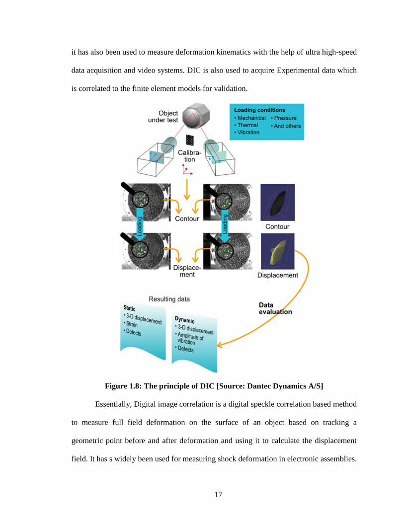
Figure 1.8: The principle of DIC [Source: Dantec Dynamics A/S] .................................. 17
Figure 2.1: Typical drop test apparatus and mounting scheme for PCB assembly .......... 28
Figure 3.1: Test vehicle used for the study and the dropping orientations. ...................... 37
Figure 3.2: Experimental set-up and schematic for controlled drop test with high
speed cameras for DIC based strain measurements. ................................................. 38
Figure 3.3: Package Strain and corresponding continuity history, with peaks in
continuity indicating failure. ..................................................................................... 39
Figure 3.4: Shematic describing methodology adopted for development of life
prediction models for leadfree solder interconnects.. ................................................ 39

x
Figure 3.5: Schematic explaining basic principle of Rainflow Counting Algorithm. ...... 42
Figure 3.6: SAC105 Pristine- Interconnect strain history and corresponding strain
amplitude histogram .................................................................................................. 43
Figure 3.7: SAC105 Thermally Aged- Interconnect strain history and corresponding
strain amplitude histogram ........................................................................................ 44
Figure 3.8: Sn3.5Ag Pristine- Interconnect strain history and corresponding strain
amplitude histogram .................................................................................................. 45
Figure 3.9: Sn3.5Ag Thermally Aged- Interconnect strain history and corresponding
strain amplitude histogram ........................................................................................ 46
Figure 3.10: SAC305 Pristine-Interconnect strain history and corresponding strain
amplitude histogram .................................................................................................. 47
Figure 3.11: SAC305 Thermally Aged- Interconnect strain history and corresponding
strain amplitude histogram ........................................................................................ 48
Figure 3.12: 3d Error Space - variation of error with „A‟ and „n‟ .................................... 50
Figure 3.13: Depiction of convergence of global minima in hybrid methods. ................. 54
Figure 3.14: Variation in initial guesses to the „A‟ and „n‟ values given as an iNput to
the algorithm. ............................................................................................................. 56
Figure 3.15: Variation of „A‟ and „n‟ values across bounded error space and error
minimization. ............................................................................................................. 57
Figure 3.16: Fatigue constants computation for Pristine SAC105 Interconnects based
on solder interconnect strain history using LM Algorithm based error
minimization. ............................................................................................................. 59
Figure 3.17: Fatigue constants computation for thermally aged SAC105 alloys based
on solder interconnect strain history using LM algorithm based error
minimization. ............................................................................................................. 61
Figure 3.18: Fatigue constants computation for Pristine Sn3.5Ag Interconnects based
on solder interconnect strain history using LM algorithm based error
minimization. ............................................................................................................. 63
Figure 3.19: Fatigue constants computation for thermally aged Sn3.5Ag interconnects
based on solder interconnect strain history using LM algorithm based error
minimization. ............................................................................................................. 65

xi
Figure 3.20: Fatigue constants computation for pristine SAC305 interconnects based
on solder interconnect strain history using LM algorithm based error
minimization. ............................................................................................................. 67
Figure 3.21: Fatigue constants computation for thermally aged SAC305 alloys based
on solder interconnect strain history using LM algorithm based error
minimization. ............................................................................................................. 69
Figure 4.1 : Schematic showing methodology adopted for development of fatigue
constants and evaluation of copper trace reliability .................................................. 74
Figure 4.2: Test vehicle schematic and photograph showing the location and layout of
traces on both sides of the board. .............................................................................. 76
Figure 4.3: 3D-Digital Image Correlation – principle ...................................................... 79
Figure 4.4: Schematic showing nature and direction of loading for accelerated testing .. 81
Figure 4.5: Contour plot (global model) showing variation of longitudinal tensile
stresses on the PCB ................................................................................................... 83
Figure 4.6 Schematic describing the finite element modeling methodology used, with
implementation of global-local submodeling ............................................................ 84
Figure 4.7: Global local submodeling: Using outputs from driving nodes of the
validated global model to drive corresponding driven nodes of the submodel ......... 85
Figure 4.8: Submodels for different straight pad-trace junction geometries .................... 86
Figure 4.9: Sub models for different angled pad/trace junction geometries ..................... 86
Figure 4.10: Multidirectional Trace Sub-models. ............................................................. 87
Figure 4.11: Comparison of strains contours as obtained by DIC and as predicted by
Finite Element Analysis. ........................................................................................... 88
Figure 4.12 : Variation of longitudinal stresses along the length for different trace
geometries ................................................................................................................. 89
Figure 4.13: Failure locations, as observed from FE simulations and accelerated tests
for straight traces ....................................................................................................... 89
Figure 4.14: Model predictions of stress concentrations and observed ............................ 90
Figure 4.15: Comparison of peak strains in different trace/pad geometries. .................... 91

xii
Figure 4.16: Increasing stress concentration with increasing difference in trace width
and pad diameter. ...................................................................................................... 92
Figure 4.17: Variation in maximum principal stress with angle made with longitudinal
direction of the board ................................................................................................ 93
Figure 4.18: Effect of trace orientation on max principal strain ....................................... 94
Figure 4.19: A comparison of stress concentrations developed at the trace-pad
junctions for angled traces. ........................................................................................ 95
Figure 4.20: Stress concentrations at sharp angles between traces. .................................. 96
Figure 4.21 : Figure showing optimum trace orientation for maximum reliability .......... 97
Figure 4.22: Fatigue curve describing the low cycle fatigue behavior of copper traces .. 98
Figure 5.1: A schematic of package-on-package stack showing both the constituent
packages viz. the bottom (PSvfBGA) and the top (CSP) packages. ....................... 103
Figure 5.2: A schematic of package-on-package test vehicle developed, showing the
three different daisy chain channels and other board attributes. ............................. 105
Figure 5.3: Schematic describing test vehicle channels and other attributes .................. 106
Figure 5.4: Single component JEDEC standard Package-on-Package test vehicle,
fabricated and used for the study. ............................................................................ 106
Figure 5.5: Schematic showing matching daisy chain net-lists on the top of the bottom
package (PSvfBGA) and the bottom of top package (CSP) .................................... 107
Figure 5.6 : Schematic showing matching daisy chain net-lists on the bottom of the
bottom package (PsvfBGA) and the PCB ............................................................... 108
Figure 5.7 : Schematics showing the classification of the two tiers of Solder
Interconnects into three daisy chain net-lists for the test component used in the
study (Source: Amkor Technology) ........................................................................ 109
Figure 5.8: Schematic of PoP stack with relevant dimensions. ...................................... 110
Figure 5.9: A comparison between regular and PoP-specific solder paste, showing a
difference in amount of transcription achieved by dipping. .................................... 112
Figure 5.10: Process flow adopted for assembling package-on-package components
on the test vehicle .................................................................................................... 113
xiii
Figure 5.11: Mechanism of warpage due to CTE mismatch. ........................................ 114
Figure 5.12: Solder reflow defect: Excessive warpage and tombstoning resulting in
open connections ..................................................................................................... 116
Figure 5.13: Solder reflow defect: Improper reflow due to low peak temperature and
less TAL resulting in un-collapsed solder joints ..................................................... 116
Figure 5.14: Solder reflow defect: Bridging of interconnections leading to short-
circuits, resulting from high peak temperature and/or high TAL............................ 117
Figure 5.15: Solder reflow defect : Head-in-Pillow defect resulting from premature
activation of flux due to high ramp rate and failure in removal of oxide film. ....... 117
Figure 5.16: Solder reflow defect : Sliding of the package owing to high warpage due
to thermal shock ...................................................................................................... 118
Figure 5.17: Good solder interconnections obtained by optimized reflow profile. ....... 118
Figure 5.18: Different reflow profiles adopted with different parameters. The
optimum profile (Profile-2) is highlighted in red. ................................................... 119
Figure 5.19: Effect of reflow parameters on PoP assembly and induced defects. ......... 120
Figure 5.20: Schematic of experimental set-up for controlled drop test with DIC and
DAQ systems ........................................................................................................... 121
Figure 5.21: Experimental set-up for controlled JEDEC drop test using
LANSMONT™ drop test tower. ............................................................................. 122
Figure 5.22: 3D-Digital Image Correlation- basic principle [Panchagade, 2006] ........ 123
Figure 5.23: Strain repeatability through different shock events .................................. 124
Figure 5.24: Global-local Submodeling: outputs from defeatured global model used
to drive submodel preserving geometrical and material detail of the area of
interest. .................................................................................................................... 125
Figure 5.25:Detailed submodel preserving the geometrical detail and various material
layers of the PoP stack with the corner solder balls modeled in detail while all
other I/Os are modeled as Timoshenko beam elements. ......................................... 126
Figure 5.26: PoP assembly submodel- critical corner interconnect .............................. 127
Figure 5.27: Figure showing correlation between DIC and FE simulation based strain
contours on the test vehicle surface- incurred during drop event. ........................... 128

xiv
Figure 5.28: A comparison of out of plane displacements as evaluated by DIC and
predicted by FE simulations .................................................................................... 129
Figure 5.29: Strain histories extracted at the four corner interconnects in the bottom
tier of solder balls. ................................................................................................... 131
Figure 5.30: Strain histories extracted at the four corner interconnects in the top tier
of solder balls. ......................................................................................................... 131
Figure 5.31: A comparison of strain cycles experienced by solder interconnects in the
top and bottom tiers located at corner-1 as shown in schematic ............................. 132
Figure 5.32: A comparison of strain cycles experienced by solder interconnects in the
top and bottom tiers located at the corner-2 as shown in the schematic ................. 132
Figure 5.33: A comparison of maximum and minimum out of plane strains
experienced by corner solder interconnects in the bottom tier. ............................... 133
Figure 5.34: A comparison of maximum and minimum out of plane strains
experienced by corner solder interconnects in the top tier. ..................................... 133
Figure 5.35: Stress distribution in the critical corner interconnect at different time
steps during shock event. ......................................................................................... 134
Figure 5.36: A comparison of stresses induced in a corner interconnect for .................. 135
Figure 5.37: A comparison of out-of-plane stresses induced in corner PCB side
copper pads interconnect for PoP and BGA packages ............................................ 136
Figure 5.38: Figures showing failure locations as observed by cross sectioning and as
predicted by FE simulations .................................................................................... 137

xv
List of Tables
Table 1.1 Thermal and mechanical properties of various packaging materials .................. 8
Table 3.1: Package architecture of 100 I/O CABGA on test board .................................. 38
Table 3.2: Fatigue constants and life predictions.............................................................. 70
Table 4.1: Different pad/trace geometric combinations incorporated .............................. 77
Table 5.1: PoP submodel: elements and material properties used .................................. 127

1
CHAPTER 1
INTRODUCTION
1.1 Electronic Packaging Overview
The field of electronic packaging has been constantly evolving and adapting to
meet the ever accelerating demands of the consumer electronics market. Electronic
Packaging is traditionally defined as the back-end-of-the-line process that transforms
silicon based integrated circuits (IC) into functional assemblies. Packaging brings
together the fundamentals of Mechanical Engineering, Physics and Electronics towards
the development of highly functional computing devices. Development and
characterization of reliable materials for packaging and establishment of interconnections
between different layers of an electronic component has remained the cornerstone of
leading research in electronic packaging for the past few decades. Leadfree and halogen-
free solder alloy materials in particular have attracted great research attention. Their
compliance with recently established Restriction of Hazardous Substances directive
(RoHS) has accounted for their proliferation throughout the packaging industry.
Furthermore, their high degree of comparability with conventional tin-lead based solder
alloys with regard to manufacturability and production has made them quite acceptable as
primary soldering materials. But, much waits to be explored as the reliability concerns
associated with these novels materials have started to surface.

2
Gordon Moore, co-founder of Intel, referring to the state-of-art in the
semiconductor industry, famously stated in 1965 “The amount of transistors which can be
inexpensively placed on an Integrated Circuit device doubles every 18 months". The
statement, initially made in the form of an observation and forecast, has since been
widely accepted and become the trend driving the semiconductor industry [Moore et al,
1998].
The electronic packaging industry is not oblivious to the market trends that drive
the semiconductor industry, its similarities with which tread a very fine line. With
decrease in IC feature size and consequential reduction in cost per IC, there is an
evolving need for cost-effective and reliable packaging solutions also. While the future
IC chips are predicted to be larger in size and to have more I/Os, the advancements in
electronic packaging are consequentially going to be driven by the market requirements
for cost-effectiveness, miniaturization and high functionality. In compliance with the
consumer electronics market trends, as the products continue to become smaller and more
functionally packed, exhaustion of horizontal packaging space has further led to
development of 3D stacking solutions. 3D package or die stacking provides more
functionality in smaller dimensions through expanding packages in the vertical
dimension. System-In-Package (SiP) architectures are being widely accepted as a
solution to system integration. System-in-Package incorporates electronic and non-
electronic devices such as optical (cameras, proximity sensors), and Micro-Electro-
Mechanical-Systems(MEMS) devices (such as accelerometers and gyroscopes), and their
interconnections in a single package, to form smart structures. With these fast paced
developments in the Electronic packaging industry, the reliability aspects of novel

3
systems need to be thoroughly addressed before they can be introduces in commercial
products.
Figure 1.1: Electronic packaging industry: Trends
[Adapted from JISSO Japan Technology Roadmap, 2001 Edition and S.L. Buedo
(Universidad Autonoma de Madrid)]
Electronic Packaging Systems can be broadly classified either on the basis of their
mounting type as 1) Surface Mount Components and 2) Through Hole Components; or
on the basis of their packaging type as 1) Hermetically Packaged or 2) Plastic
Encapsulated packages. The former classification of electronics packaging is the most
widely accepted.
Thru Hole•DIP•PGA
Surface Mount•QFP•TSOP•SOJ•BGA
Chip Scale•CSP•Flip Chip•WLP
3D Packaging?
•PoP•Stacked Die

4
Figure 1.2: Different types of electronic packages, classified according to their
mounting type and lead structures. [Source: Renesas Electronics Corporation]
Surface Mount Type
Area Array Package
Gull Wing Lead Package
Non-Lead Package
J-Lead Package
Passive Devices
BGA,FBGA,HFBGA,HBGATHBGA,LBGA,TFBGA,
VFBGA
TFLGA
QFP,HQFP, LQFP,HLQFP,TQFP,
HTQFP
SOP, SSOP,HSOP,HSSOP,
LSSOP,TSSOP
VQFN, HVQFN, WQFN, HWQFN
VSON, WSON, HWSON
SOJ, QFJ
SC-62, SC-70, SC-74, SC-
88, TSSOP, HWSON, LDPAK, DPAK, D2PAK,
UFP, URP
DIP, SDIP, SIP, ZIP
TO-3P, TO-220, DPAK(L),
LDPAK(L)
Lead type Package
Passives
Pin – Insertion Type

5
Figure 1.3: Increasing complexity and performance capabilities of modern chip-
carriers. [Source: Corporate Package Development, STMicroelectronics]
For facilitating ease of identification electronics are further classified within a
system. The electronic packaging hierarchy classifies an electronic system in four levels.
The zeroth level constitutes non-repairable parts, such as integrated circuits or passive
devices. The first level identifies small components such as BGAs and QFPs which house
the zeroth level devices and are mounted on PCBs daughter-cards. The second level
packaging constitutes the PCBs that house different second level packages together into
one functional unit. Lastly, the third and highest level of packaging identifies
motherboards and pullout chassis on electrical cabinets which house several PCBs
together to form a standalone electrical unit. The interconnects between the zeroth (chip)
and the first (package) level of packaging are the wire-bonds. These are referred to as
first level interconnects while the solder balls or leads, which connect the packages to
their landing pads on the PCB are called second level interconnects.

6
Figure 1.4: Hierarchy of electronic packaging. [Adapted from ‘Mechanical Design
of Electronic Systems’ by Dally, Lall and Suhling, 2008]
Silicon Wafer
IC Chip
First Level Package(BGA)
Second Level Package
(PCB or Card)
Third Level Package(Motherboard)
First Level Interconnect(Wirebonds)
Second Level Interconnect(Solder Balls)
7
1.2 Reliability Concerns.
Driven by the trends towards miniaturization and increased functionality, the
electronic components are being made smaller and more complex. With advent of novel
packaging technologies such as System-on-Chip (SoC), System-in-Package(SiP), Multi-
Chip-Modules (MCM) and 3D packaging technologies such as PoP and Stacked-Die
components, the complexity of packaging architectures has exponentially increased. As
the interconnect counts increase and the pitch between them decreases, their
susceptibility to failure increases. In the highly competitive electronics market, it is of
outmost importance to the manufacturers to ensure highest levels of quality and reliability
in usage conditions representative of the real world.
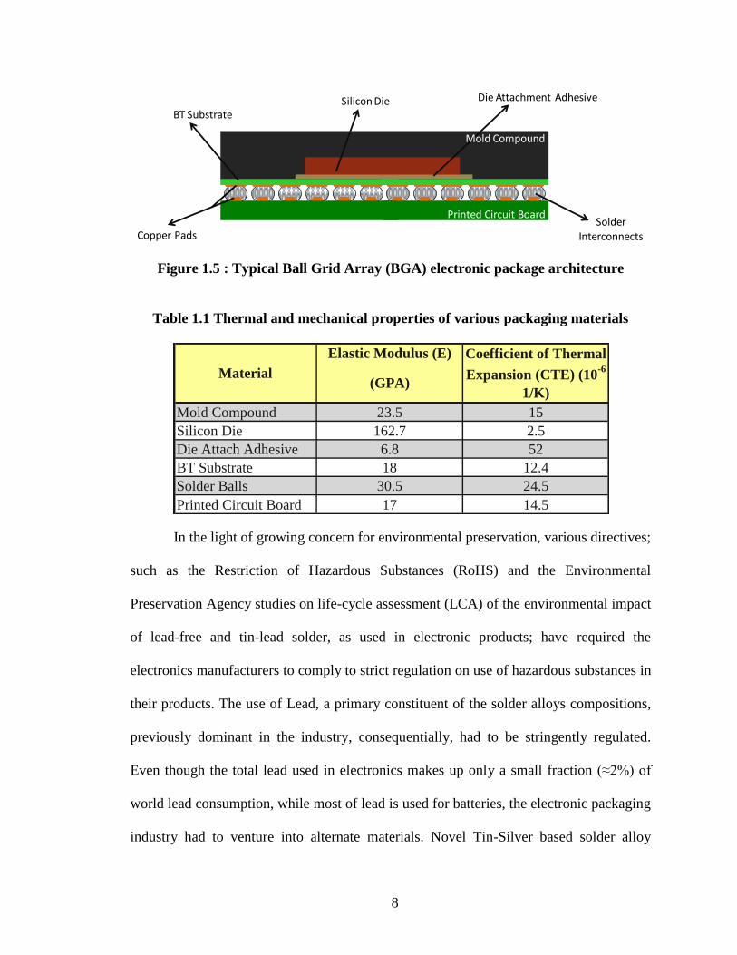
A typical electronic package comprises of various different types of materials
(Figure 1.5) with vastly varying material properties. For accurate reliability
quantification, it is very import to have a clear understanding of how all these constituent
materials of a component interact with each other during the products operational life. As
an example, automotive electronic components such as Engine Control Unit (ECU)
housed near the engine experience harsh thermal cycling during their operational life.
These extreme thermal conditions lead to severe expansion and contraction of the
components. A high degree of mismatch between different constituent layers of the
package can often lead to delamination between layers and shearing of the interconnects.
As another example, electronic components housed in portable electronic devices often
experience shock pulses when the product is dropped. A careless design which does not
allow for any compliance to deformation under shock-loading may result in drastic
failure of the component and as a result the whole device.
8
Figure 1.5 : Typical Ball Grid Array (BGA) electronic package architecture
Table 1.1 Thermal and mechanical properties of various packaging materials
In the light of growing concern for environmental preservation, various directives;
such as the Restriction of Hazardous Substances (RoHS) and the Environmental
Preservation Agency studies on life-cycle assessment (LCA) of the environmental impact
of lead-free and tin-lead solder, as used in electronic products; have required the
electronics manufacturers to comply to strict regulation on use of hazardous substances in
their products. The use of Lead, a primary constituent of the solder alloys compositions,
previously dominant in the industry, consequentially, had to be stringently regulated.
Even though the total lead used in electronics makes up only a small fraction (≈2%) of
world lead consumption, while most of lead is used for batteries, the electronic packaging
industry had to venture into alternate materials. Novel Tin-Silver based solder alloy
Mold Compound
Printed Circuit Board
Silicon Die Die Attachment Adhesive
Copper PadsSolder
Interconnects
BT Substrate
Elastic Modulus (E)
(GPA)
Mold Compound 23.5 15
Silicon Die 162.7 2.5
Die Attach Adhesive 6.8 52
BT Substrate 18 12.4
Solder Balls 30.5 24.5
Printed Circuit Board 17 14.5
Material
Coefficient of Thermal
Expansion (CTE) (10-6
1/K)

9
compositions were developed to address the issue. However, their adverse effects on
product reliability and high cost of compliance were widely cited as criticisms of these
alternative materials. In the recent past, the high volume of research on the behavior of
leadfree solders and their reliability has helped in development of a better understanding
of their performance. However the reliability data available on these materials is still very
limited and does not suffice to establish a comprehensive comparison with Lead-based
alloys.
In today's world, electronic systems are omnipresent and in many cases, they
enable core functionality of the devices that encompass them. With electronic
components residing at the heart of most of the mission-critical systems of the modern
age- such as Air Traffic Control , Personal and Mass Communication Systems and
Transportation, it is of outmost importance that the reliability concerns related with them
be thoroughly addressed. Unlike mechanical constituents, of any system, electrical
components generally do not wear out. Their failure is often undetectable before it
occurs. The main reliability concerns associated with electronic components are
associated with the following causes:
1. Thermally Induced stresses due to exposure to high operating temperatures
2. Mechanically Induced stresses due to careless handling-drop; and operation in
vibrating environment.
3. Residual stresses from manufacturing processes
4. Electro-migration, Transient static discharge and other electrically induced
failures.

10
With regard to the mechanical failures, especially those caused due to thermally
or mechanically induced stresses, the interconnects between various levels of a
component are rendered most vulnerable to failure. Furthermore, since they form a very
significant part of a component, their failure can result in drastic failure of the whole
component. This thesis encompasses reliability studies carried out on electronic
component interconnects with special focus on second level interconnections. While the
state-of the-art lies in diagnostic methods which reside in post-failure space. This work
addresses the growing need for prognostic and life-prediction methodologies which
enable failure isolation before occurrence.
1.3 Vibration and Shock Reliability
Portable computing and communication devices, omnipresent in today‟s world,
constitute a major application of electronic components. Furthermore, emerging trends
for smaller and lighter form factors have driven the electronic component industry
towards robust designing or withstanding high shock and vibration environments. With a
high probability of careless handling at the hand of the consumer, the electronics industry
cannot undermine the importance of mechanical robustness of their products. The
reliability issues associate with the interconnections between various electronic
components of a product, especially, are of most importance since they are most
susceptible to failure under harsh environments.
For an assessment of the reliability of electronic components under drop and
shock conditions representative of the real-world usage conditions, various testing
procedures have been standardized. For evaluation of their reliability in vibration

11
environment, various different vibration profiles have been established to serve as
representation of actual environment in which a component is intended to be deployed.
Test methods used for Drop/Shock reliability quantification can broadly be classified as
board-level and product-level tests, under constrained and unconstrained (free drop)
conditions. The most widely accepted board level constrained drop test, is the one
developed by the Joint Electron Device Engineering Council (JEDEC). The JEDEC test
standard “Board Level Drop Test Method of Components for Handheld Electronic
Products”, JESD22-B111, is used by electronics manufacturers to evaluate the
performance of surface mount components in drop/shock.
Figure 1.6: Vibration testing profiles for survivability assessment of electronic
components [Ref: MIL-STD-810F]

12
Figure 1.7: JEDEC standard shock pulse [Ref: JEDEC, JESD22-B111]
The standards established for reliability quantification however, adopt a highly
conservative approach. The tests, like the one outlined in JEDEC standard JESD22-B111,
subject the test vehicle to a very harsh shock pulse with constraint conditions resulting in
high level of deformations. Consequentially, mapping of the standard test results to
product level performance is very challenging. While a component may perform
relatively worse in a standard test, it might turn out to survive through its service life
when deployed in the field, since in an actual product, the component failure mode and
time of occurrence is dominated by its housing design and the level of shock its subjected
to; which may vary with –say, different drop orientations and heights. Additionally,
factors such as the product mass, structural compliance etc also play a vital role in
affecting the shock pulse that the component finally experiences. Despite the availability
of standard testing procedures, the component deigns process is still very challenging,
owing to the possibility of a multitude of failure inducing environments that the product
much can be subjected to-each of which the product cannot be tested for. It is very
difficult to analyze various design variations, of a product by subjecting each variation to
exhaustive testing procedures. An underlying theme of this thesis is development of life-

13
prediction models and design guidelines which eliminate the need of such exhaustive
testing procedures and aid in speeding up the product development cycle.
1.4 Finite Element Modeling for Transient Dynamic Simulations
In the highly competitive electronics market, the product development cycles are
continuously shrinking. New technologies are being rapidly developed and introduced
into the products at unprecedented rates. Conception-to-Production times have
substantially shrunk as novel technologies continue to make older ones obsolete within
the span of a few months. With tight production schedules and small product
development cycles, exhaustive testing of all the design iterations of a product has
become unfeasible. Owing to the complexities involved in in-situ measurement of Solder
joint response to the transient dynamic shock phenomenon, analytical methods have
established their superiority over experimental methods.
Finite element methods in particular have gained popularity in the electronics
industry, in the development of new packaging materials, designs and assembly
processes. The analytical method involves discretization of a continuous structure into
„finite elements‟ governed by specific material models. When carefully devised and
validated with experimental observations, the technique is capable of accurately
simulating material responses to static as well as transient dynamic events. Various Finite
Element modeling approaches have been used to address reliability issues specific to
electronic packaging [Dally 2008]:
1. Equivalent layer models to represent the solder joints and simulate their
behavior under drop impact.

14
2. Solid-to-solid sub-modeling techniques to analyze BGA reliability for drop
impact using half the PCB board.
3. Shell-to-solid sub-modeling using beam-shell-based quarter symmetry model
to reduce the computational time.
4. Symmetry of load and boundary conditions is used to obtain computational
efficiency and decrease the model size.
The FE method based simulations make it easier to account for scale differences
between the dimensions of the individual layers of an electronic assembly, such as the
solder interconnects, copper pad and chip interconnects. [Dally, 2008]. I the past, several
techniques to simulate electronic packaging subjected to shock pulses such as those
induced by drop testing test have been developed. To this effect, in addition to employing
implicit FE method by translating the input acceleration pulses into effective support
excitation loads on the test vehicle; [Yeh 2004], researchers have also used the explicit
finite element solver to simulate transient dynamic event [Lall 2004, 2005, Xie 2002,
2003, Wu 1998, 2000]. Explicit time integration serves as a better approach to transient
dynamic deformation of electronic assemblies since it approximates the phenomenon as a
wave propagation problem. The governing equation for a dynamic system can be
expressed as [Cook 1989]:
n
ext
nnn RRDCDM int (1.1)
For a linear problem, {Rint
}n=[K]{D}n, where [M], [C] and [K] are the mass,
damping and stiffness matrices respectively and {D}n is the nodal displacement vector as
each time step. Methods of explicit direct integration calculate the dynamic response at

15
the time step (n+1) from the equation of motion, using the central difference formulation
and known conditions at one or more preceding time steps as shown below [Cook 1989]:
122
int
12 2
112
2
11
nnnn
ext
n DCt
Mt
DMt
RRDCt
Mt
(1.2)
Other FE techniques used in electronic packaging reliability studies include
implicit global models[Irving 2004, Pitaressi 2004, Syed 2005], global-local submodeling
[Wang 2004, Tee 2003, Wong 2003, Zhu 2001, 2003, 2004], smeared property models
[Jie 2004, Lall 2006] and explicit-implicit sequential model [Zhu 2005]. The global-local
submodeling is a very powerful approach which significantly reduces the computational
time by dividing a model into two parts. In the first run, a defeatured „global model‟ is
created and used to simulate the phenomenon using boundary conditions representative
of the actual test. Subsequently, detailed „submodels‟ of the area of interest are
developed. These submodels preserve the geometric and material intricacies of the area
of interest in complete detail. The outputs from the global model simulation are extracted
at key locations and provided as driving inputs to the submodel. The Finite Element
method has been extensively used for simulating transient dynamic phenomenon in
electronic assemblies, in the studies presented in this thesis.
1.5 Digital Image Correlation
With the ease in availability of low-cost and easy-to-use hardware and software
facilities for digital image acquisition, digital image analysis, nowadays, is becoming
extremely popular in experimental mechanics. It is widely used in strain field

16
measurement as a powerful tool to post-process fringe images generated by moiré effect
or other interferometry methods.
High speed photography has been used to measure deformations in sheet metal
forming, Automotive crash testing, rail vehicle safety[Kirpatrick, 2001], air-plane
safety[Marzougui, 1999], modal analysis of turbine blades, high strain rate Split-
Hopkinson bar tests, dynamic fracture phenomenon, and package hermiticity (MIL-STD-
883) tests. High-speed cameras measure impact speed, force, and deformation due to
shock, and thermal loading. Previously, the measurement of derivatives of field
quantities, such as strains, was limited to a specific physical locations or discrete target
points in an electronic structure. It was not feasible to extract data at a very large number
of locations by using discrete targets because of the time consuming nature of the
process.
Digital Image Correlation (DIC) is a state-of-art technique which overcomes such
limitations of other optical methods. A major advantage of the technique is that the
sample preparation is simple and quick. To prepare the specimens for testing, they are to
be speckle painted, which can be easily done using spray paint. Transient deformation
data can then be recorded with the help of high-speed cameras, which is then processed to
evaluate full-field strains. In electronic packaging science, digital image correlation has
been used to study various mechanical phenomenon such as stresses in BGA package
solder interconnects under thermal loading[Zhou 2001; Rajendra 2002; Zhang 2004
2005; Xu 2006; Lall 2009, 2010], material characterization at high strain rates [Tiwari
2005, Lall 2010], crack propagation in solder interconnects in drop/shock [Lall, 2009,
2010] and strains in flip-chip dies under thermal loading [Kehoe 2006]. In the recent past,
17
it has also been used to measure deformation kinematics with the help of ultra high-speed
data acquisition and video systems. DIC is also used to acquire Experimental data which
is correlated to the finite element models for validation.
Figure 1.8: The principle of DIC [Source: Dantec Dynamics A/S]
Essentially, Digital image correlation is a digital speckle correlation based method
to measure full field deformation on the surface of an object based on tracking a
geometric point before and after deformation and using it to calculate the displacement
field. It has s widely been used for measuring shock deformation in electronic assemblies.

18
The technique works by comparing a sub image around a reference pixel in the
original/reference image and then comparing it with the sub images corresponding to
different pixels in the deformed image using a predefined correlation function to describe
the difference of the two digital sub images. A full field displacement contour is obtained
by shifting the reference pixel in the original image and applying this method to all the
other pixels of the images. It is therefore obvious that the resolution/accuracy of the DIC
procedure relies on the pixel size of the camera image. The technique is described in
further detail in Chapter 3 of the thesis.
1.6 Thesis Layout
This thesis presents reliability studies performed on various electronic component
structures. The aim of this work was to develop Finite Element models to simulate
transient dynamic phenomenon in electronic assemblies with special focus on solder
interconnects. Using FE simulations, validated with experimental measurements, the
work aims at development of life prediction models and design guidelines which
eliminate the need for exhaustive testing during the design iterations and aid in
shortening the product development cycle.
Chapter 2 presents literature survey on solder joint reliability. Experimental
methods used in electronic packaging reliability studies and various life prediction
models used in electronics. A major portion of this work deals with reliability o second
level interconnects. The chapter therefore outlines previous research carried out in this
field in order to differentiate the work presented in this thesis. Board level reliability
studies carried out on BGA packages in particular have been emphasized. Previous work

19
pertaining to the drop/shock and vibration performance of the novel lTin-Silver based
leadfree solder alloys has also been presented. The import of the work presented
herewith, in context of its applicability to and usefulness in product development cycles,
the current state-of-art in electronic packaging reliability studies has been summarized.
The following Chapter 3 presents a study carried out a BGA test vehice with three
different lead free alloys system used for solder interconnects –with an aim to develop a
life prediction model for these interconnects in drop/shock environments. The chapter
describes the tests carries out on pristine and thermally aged test vehicles and compares
their performance in drop tests. The methodology adopted to evaluate a set of fatigue
constants; which govern the mathematical life prediction model; including a non linear
least squares minimizing algorithm, the Levenberg-Marquardt (LM) algorithm, has been
described in detail. Finally, the chapter validates the accuracy of the life prediction model
developed and advocates its applicability to product development cycles.
In the following section, Chapter 4, reliability studies carried out on an indigenous
test vehicle – developed with an intention to study PCB surface Copper Traces- have
been presented. The chapter details the test vehicle attributes, the experiment designed to
study the effect of variations in copper trace attributes on their reliability in drop and
shock and the strain-life based power law developed to describe copper trace fatigue.
Conclusively the study along with presenting a fatigue life prediction model, summarizes
the effects of PCB surface copper trace orientations and dimensions on their reliability.
Design guidelines for laying out copper traces on the PCB surface, ensuring maximum
reliability have been suggested for use as empirical rules.

20
Chapter 5 encompasses studies carries out on novel Package-on-Package (PoP)
components. While the current state-of-art resides in manufacturability issues associated
with PoP structures, the chapter addresses the need for a reliability quantification of PoP
structures. The study describes in articulate detail the methodology adopted to fabricate
the PoP test vehicle as per JEDEC standards. While presenting an analysis of the e
hurdles faced during the test vehicle fabrication, in the form of reflow-related defects, the
study also serves to standardize an optimum reflow profile for fabrication of PoP
assemblies. Later part of the chapter deals with development of detailed global-local FE
models for simulating the PoP structures‟ response to standard drop tests and provides an
insight into the failure mechanisms of these novel structures. In conclusion, the study
compares the reliability issues associated with PoP assembly and reliability in drop and
shock scenarios and compares them with an equivalent BGA. Finally, the concluding
Chapter 6 summarizes the purpose and findings of the thesis and briefly discusses the
scope for future work.

21
CHAPTER 2
LITERATURE REVIEW
In the age of communication technology, electronics are omnipresent. With the
ever increasing significance of electronics, the import of their reliability is also
increasing. Lately, the prime focus of packaging research has shifted from manufacturing
processes to reliability issues involved with electronics. This chapter entails a background
of the research done on electronic packaging reliability; with a special focus on BGA
reliability in drop/shock environments; and summarizes recent developments in
predictive failure modeling for the same.
2.1 Solder Joint Reliability
Since the Interconnects perform a critical function of communicating between
functional parts of a package, they form a vital part of the electronic assembly.
Additionally, the fact that they the most mechanically complex part of the assembly and
their miniature form, render them most vulnerable to failure. The solder interconnects
between the package and the PCB, experience the highest susceptibility to failure under
harsh loading conditions and upon failure, render the device irreversibly useless. The
quality and reliability of solder interconnects are often considered an index of the
reliability of the package on the whole. [Woodgate, 1987] described a perfect joint as

22
one showing complete wetting of solder to its corresponding pad- outlining this as a
universal requirement that applies to both through-hole and surface mount assemblies.
The pursuit of component miniaturization with increased functionality had led the
industry towards fine pitch components. With the need for increasing interconnections
between packages and PCB, and owing to the limitations of manufacturing processes,
when the pitches between the legs of perimeter array surface mount components could
not be reduced any further, area array assemblies were conceived. Over the years, area
array surface mount components have evolved from primitive Pin-Grid-Arrays to novel
Ball-Grid-Array packages. BGAs, which have now proliferated through the packaging
industry, cater to the need of high I/Os and reliable interconnects between the packages
and the PCB, by accommodating them in a very small form. Furthermore, their ease of
fabrication and comparable robustness has established them as suitable replacements for
area array surface mount components.
In addition to providing electrical connectivity, the solder joints of a BGA
component also preserve the mechanical integrity of the component by serving as
compliant structures between the component and the PCB. As a result, the solder
interconnects consume a large portion of the mechanical damage caused to the assembly
in a drop/shock event. Rapid shearing caused due to CTE mismatch between the
component and the PCB in thermal loading scenarios and cyclic fatigue at high strain
rates during shock events are attributed as major causes of failure in solder joints.
In terms of their thermal performance, [Chiang 2000] suggested two reflow
passes as a means to achieve better reliability characteristic of BGA type packages. A
twofold increase in their characteristic life when subjected to thermal cycling due to

23
significant reduction in equivalent plastic strain, the energy density and the Von-Mises
stress of the solder joint was shown. Different package architectures variables and their
effects on BGA solder interconnect reliability have been articulated [Syed, 1996]. The
improved solder joint reliability of perimeter array packages over area array packages has
also been established [Syed, 1996]. Syed, also reported on the direct impact the BT
substrate thickness had on solder joint reliability- thicker BT substrate, he reported,
enhanced the solder joint reliability.
Previously, it has been shown that large fillets and low standoff heights of the
BGA solder joints leads to an increase in their fatigue life under power cycling [Charles
1990]. It has been shown that large fillet angles serve to reduces high magnitudes of
stress concentrations as they result in an increased the net cross-sectional area within the
joint. While the corner solder balls, have been shown to be most vulnerable to failure in
drop/shock scenarios, it has been shown that the layout of solder balls is very critical
since it affects the load distribution on critical solder ball [Tee 2004].The effects of solder
ball metallurgy and the inter-metallic compound (IMC) thickness at the solder-copper
interface have been looked into [Zhong, 1999]. The effect of the pad surface finish has
alse been researched, [Bradley 1996 and Suhling 2002] showed superior HASL pad
finish thermal reliability performance over immersion nickel and palladium based pad
finishes for BGA packages.
2.1.1 Lead-Free (Pb-Free) Solders
In light of growing concern for the environmental effects of hazardous materials,
directives such as the Restriction of Hazardous Substances (RoHS) and Waste from

24
Electrical and Electronic Equipment (WEEE) have restricted the use of lead-based
components in electronic manufacturing industry. The advent of Pb-Free alloys in the
packages industry while inevitable at first, has now been widely accepted. A vast
multitude of lead-free alloy compositions have been studied for their applicability in
electronics. The Tin-Silver-Copper (Sn/Ag/Cu) often referred to as SAC family of alloys
have been established as one of the most suitable replacements for their leaded
counterparts.
Previously, researchers have outlined the variation in SAC alloy performance
with different packaging architecture, in addition to underlining their strong temperature
dependence [Syed 2001, Zhang 2003 and Vandevelde 2004]. Lowering the silver content
in the SAC compositions has been shown to result in a significant improvement in their
board level reliability in drop/shock testing. In contrast, researchers [Zhang 2008 and
2009] have shown that higher silver content SAC alloys have enhanced thermal
reliability. The SAC alloy performance has been compared with conventional leaded
solder compositions [Schubert 2003 and Clech 2005]. Experimental studies conducted
have shown that a significant enhancement in SAC based solder-joint reliability can be
achieved by using compliant plastic substrates.
With regard to their effect on drop/shock performance, researchers have
investigated the effects of variation in lead-free solder alloy composition on their
reliability. SAC alloy compositions with low silver content have been shown to be
resistant to high strain rates under mechanical shock and to have improved drop
reliability [Zhu 2008, Che 2008, Lall 2008a, Pandher 2008, 2007, Kim 2007].
Additionally, it has been shown that by lowering the silver content of SAC alloys, an

25
increase in their creep rate, can be achieved [Zhang 2008]. Researchers, [Song 2008,
Huang 2007] have suggested adding Ni to SAC alloys to improve thier drop reliability. It
has also been shown that an improvement in their drop performance can be achieved by
using SAC interconnects on Ni/Cu/Au surface finishes [Kawashiro 2008]. Solder joint
reliability has been shown to enhance with UBM/penetration layer/SnAg lead free solder
bump structures [Choi 2007]. While a lot of research has been conducted on the effects of
Pb-free alloy compositions on their drop/shock performance, the life prediction models
for Pb-free alloys presented in this study, are largely beyond the state of art.
2.2 Drop and Shock Testing
Owing to their small form factor and light weight, portable electronics are highly
susceptible to mechanical shocks due to accidental drop. Solder interconnects between
different components in a handheld electronic product are the most susceptible to failure
in such scenarios. Mechanical characterization of the interconnects and an assessment of
their reliability in shock environments is critical to their long term survivability in the real
world.
Since the electronic components housed in modern electronics are packed with a
high level of functionality, the operating temperature in these devices; due to power
dissipation; often rise to harmful levels in the vicinity of the packages. Presenting an
insight into the effects of overlapping thermal and mechanical stresses on their reliability,
Mattila et. al. [Mattila 2007], have investigated the effects of temperature on the drop
tests reliability of BGA components. Lall et. al. [Lall 2006, 2009] have also investigated
the effects of overlapping stress due to thermal and mechanical loading on packaging by

26
subjecting them first to thermal loading followed by drop tests. While a most realistic
approximation of their performance in real world can only be obtained by conducting
product level tests, these tests are often very expensive and accounting for small design
variations by conducting exhaustive testing is very time consuming. Package-level tests,
which act as simplified real life impact scenarios are therefore performed to serve as an
acceptable replacement of board-level drop tests that save cost and time [Yeh 2005, 2006,
Ong 2003]. For their reliability assessment, electronic components are subjected to a
vaiety of board level tests such as bending impact [Kim 2006], ball impact [Lai 2006],
pendulum impact or Charpy [Ratchev 2007], high speed bend [Seah 2006], microimpact
[Ou 2005], cold ball pull and high speed shear tests [Johnson 2007]. These tests have
been performed to serve as tools to study impact toughness, fracture toughness and other
contributing factors that directly impact the shock reliability of electronic components.
Amongst the mechanical tests mentioned, the drop test is the most prominent. JEDEC has
standardized the drop test [JEDEC 2003] by specifying the drop impact pulse and test
board configuration. The standardized test serves as a common ground for assortment of
semiconductor component manufacturers to compare the solder joint reliability under
impact. The JEDEC standard drop test however has its limitations, in that it has too many
redundant loading conditions, which result in reduced sample sizes of each loading
condition for statistical analyses. Zhao et. al. [Zhao 2007] addressed this limitation of the
testing standard by proposing an alternative board design with only one loading condition
and a sufficiently large sample size, while applications of the response spectra to a
JEDEC standard drop test board subjected to different JEDEC drop test conditions Tsai
et. al. [Tsai 2007] have also been demonstrated.

27
The JEDEC standard specifies that the test vehicle should be mounted with the
package side facing downwards to create a more critical loading condition [Yeh 2004].
As per the test, the drop orientation of the test vehicle is required to be horizontal or at
zero degrees during the drop test. However, the drop orientation standardized by JEDEC
may not be the only orientation in which the test board may fall in a real world scenario.
Additionally, the supports and clamps to the board as outlined in the standard are too
generic to be representative of the actual clamping conditions in a product housing.
Experiments conducted on cell phones by Liu et. al. [Liu 2005], Seah et. al. [Seah 2002]
and Ong et. al. [Ong 2003] have underlined the sensitivity of impact reliability to the
impact angle of the product. Chong et. al.
Despite its limitations, the JEDEC standard continues to be the most widely
accepted drop test standard. The following figure shows the schematic of a JEDEC
standard drop test of a printed circuit assembly as outlined in JEDEC JESD-B111.

28
Figure 2.1: Typical drop test apparatus and mounting scheme for PCB assembly
(Source: JEDEC)
2.3 Finite Element Modeling for Transient Dynamic Simulations
The Finite Element Method, owing to its versatility and accuracy in simulating
complex mechanical phenomenon, has been exploited for reliability prediction in
Electronic Packaging. The FE method had been used to make solder joint life predictions
under different loading scenarios such as thermal cycling, drop and shock, vibration and
bending. A vast majority of the life prediction models based on the finite element

29
method, account for the reliability of the components based on accumulated field
quantities(deformations) and their derivatives such as like creep strain, inelastic strain
energy density and nonlinear plastic work.
Previous researchers have employed several modeling methods to simulate
transient dynamic events. Researchers have used smeared property models [Lall 2004,
2005], Timoshenko beam models with conventional and continuum shell [Lall 2006,
2007, 2008], global-local submodels [Tee 2003, Wong 2003, Zhu 2003, 2004] and
Implicit transient analysis with Input-G Method [Luan 2004] for simulating electronic
packages subjected to mechanical loadings.
[Wang 2001] applied [Anand 1985] unified creep model to represent viscoplastic
deformation behavior of solders. He concluded that inelastic deformation behavior
calculated by the model can be applied for solder joint reliability predictions. [Zhang
2000] proposed a novel life prediction model that takes into account the damage
evolution to accurately predict solder joint reliability. Tee et.al. [Tee 2004] used the
maximum normal peel stress of the critical solder joint extracted from finite element
simulation as a failure criteria and presented a life prediction model to quantify package
reliability by estimating the number of drops to failure for a package subjected to board
level drop tests.
Since bending is one of the prime causes of failure in electronic components
mounted on PBC surface, Shetty et.al. [Shetty 2003] used three-point and four-point
bending tests for evaluating the reliability of chip scale packages under curvature
loads. In
the study, deformation energy based empirical reliability model was used to calculate
mean life time to failure, under mechanical bending. The study further established a

30
relationship between average cycles to failure and average strain energy density by
volume averaging the strain energy density over the top layer of the solder joint using the
volume average technique proposed by [Zhan 20003, Darveaux 1992 and 2000]. In this
study, the FE method has been extensively used to simulate transient dynamic as well as
static mechanical phenomenon and to make reliability predictions for solder interconnects
in drop and shock.
2.4 Digital Image Correlation
Owing to the complexity of electronic assemblies, it is not feasible to place
deformation measuring devices such as strain gages on them. Additionally, conventional
deformation measuring techniques only evaluate localized values. With a multitude of
components on a single test assembly, it is beneficial to have an estimate of full field
deformations for subsequent evaluation of individual component response.
Digital Image Correlation (DIC) is a novel technique which works by tracking a
geometric point on the specimen before and after deformation, thereby enabling full field
strain and displacement measurement during a transient dynamic event. Geometric points
on the test specimen are distinguished by speckle coating the surface of interest. Previous
studies have established the effect of size, consistency and density of the speckle pattern
on the accuracy of the method [Zhou 2001, Amodio 2003, Srinivasan 2005]. The DIC
method has its merits over strain measurement by using strain gage, which measure strain
only at localized points on the specimen. Furthermore, the technique does not involve
contact with the specimen during the monitored event and specimen preparation is very
quick and easy.

31
The Digital Image Correlation technique has been extensively used in this work to
measure field quantities (deformation) and for subsequent calculation of their
derivatives(strain). The technique has been employed in this work, in conjunction with
high speed imaging systems to evaluate transient dynamic board response to JEDEC
standard shock events as well as static bend tests.
High speed photography has previously been used to measure deformations in
sheet metal forming, Automotive crash testing, rail vehicle safety[Kirpatrick, 2001], air-
plane safety[Marzougui, 1999], modal analysis of turbine blades, high strain rate Split-
Hopkinson bar tests, dynamic fracture phenomenon, and package hermiticity (MIL-STD-
883) tests. High-speed cameras measure impact speed, force, and deformation due to
shock, and thermal loading. Previously, the measurement of derivatives of field
quantities, such as strains, was limited to a specific physical locations or discrete target
points in an electronic structure.
In the field of electronic packaging, DIC has been used to calculate full field
deformations and deformation gradient in electronics [Lall 2007c, 2008b-d, 2009, Miller
2007, Park 2007a,b, 2008]. Previously, the DIC based strain measurements technique has
been demonstrated to be useful for transient strain measurement in electronic assemblies,
in the presence of rigid body motion Lall 2007 2008]. Digital image correlation also been
employed to study deformations in printed circuit assemblies for mobile devices [Lall
2007, Miller 2007, Park 2007], material characterization [Jin 2007, Park 2007, Thompson
2007], for evaluation of stresses and strain in flip-chip dies under thermal loading [Kehoe
2006] and for calculating stresses in solder interconnects of BGA packages under thermal
loading conditions [Zhou 2001, Yogel 2001, Zhang 2004, Zhang 2005, Sun 2006]. DIC

32
has also been used for evaluating elastic modulus of underfill materials at elevated
temperatures during four-point bending tests [Park 2007a, Shi 2007]. In conjunction with
high resolution SEM, the method has also been used to study the stresses released at the
component surface before and after ion milling [Vogel 2007].
Although the technique has been widely used in thermal analysis of electronic
packaging, it has recently gained a lot of attention in the field of transient dynamics as
well. DIC algorithms in conjunction with high speed imaging systems are now widely
used as tools for acquisition and analysis of deformation images. The technique has been
extensively used in this study for evaluation of test vehicle deformation during transient
dynamic as well as static mechanical events.

33
CHAPTER 3
FATIGUE CONSTANTS FOR LIFE PREDICTION OF SECOND LEVEL SOLDER
INTERCONNECTS SUBJECTED TO DROP & SHOCK
3.1 Introduction
Handheld electronic products such as cell phones, cameras, calculators etc are
highly susceptible to shock and drop during their service, owing to their compact form
factors. Electronic packages which constitute the most functional parts of these products
also end up being the most vulnerable to failure as a result of shock. Second level
interconnect failure has been established as the most common failure mode under
application of mechanical shock. Joint Electron Devices Engineering Council (JEDEC)
standardized drop test is one of the most common experimental methods used to quantify
shock and vibration reliability. The test involves subjecting a test board of prescribed
design, to a specified shock pulse. Owing to their small size and inaccessible feature, Dit
is difficult to measure deformations and their derivatives across interconnects using strain
gage and other conventional experimental techniques.
In the light of increasing concern for environmental preservation, lead free solder
alloys have proliferated through the electronics industry. Leadfree solder alloy systems
are being increasingly used as solder interconnects in electronic packages. It is important
to determine the life of these lead free alloy-systems in order to place them as a worthy

34
replacement for the lead based solder alloys. Previously, in order to evaluate the
reliability of lead free interconnects in different environments, representative of their
service life, they have been subjected to various mechanical tests such as drop and shock,
thermal ageing and thermal cycling. Previously, many researchers have studied the
effects of variation in solder alloy composition on their reliability. Low silver content
SAC alloys are seen to be resistant to high strain rate under drop shock and improve drop
reliability [Zhu 2008, Che 2008, Lall 2008a, Pandher 2008, 2007, Kim 2007].
Researchers have established increase in the creep rate, achieved by lowering silver
content of SAC alloys [Zhang 2008]; improved drop reliability, by adding Ni in SAC
alloys [Song 2008, Huang 2007]; improvement in the drop performance of SAC BGAs
on Ni/Cu/Au surface finishes [Kawashiro 2008]. Solder joint reliability is seen to
enhance with UBM/penetration layer/SnAgCu lead free solder bump structures [Choi
2007]. SnAgCu and SnPb based solder alloys on OSP are seen to have similar fracture
energy at lower shear speed. As shear speed increases however; beyond 100mm/sec
fracture energy of SAC is seen drops to zero [Sweatman 2008].
In this chapter, the concept of relative damage-index based on the lead-free
interconnect transient strain history; evaluated using Digital Image Correlation and
Explicit Finite Element Analyses; has been established for life-prediction of leadfree
solder interconnects . Solder alloy systems studied include Sn1Ag0.5Cu (SAC105),
Sn3Ag0.5Cu (SAC305) and 96.5Sn3.5Ag. Transient full field strains on the test board
surface, during the shock-impact have been measured using Digital Image Correlation in
conjunction with high-speed cameras operating at very high frame rates (≈50000 fps). In
addition the effect of sequential stresses due to thermal aging and shock-impact on the
35
failure mechanisms of the interconnects has also been studied. Previous researchers have
attempted evaluation of transient dynamics at the board and component-levels using
various simulation techniques including, explicit finite-elements [Lall 2004, Xie 2002,
2003, Wu 1998, 2000] implicit global models [Irving 2004, Pitaressi 2004], and global-
local sub-models [Tee 2003, Wong 2003, Zhu 2001, 2003, 2004]. Life prediction of new
lead-free alloy-systems under shock and vibration however, is largely beyond the state of
art.
In this study, explicit sub-modeling and DIC based transient strain histories of the
solder interconnects have been used to develop life prediction models for solder
interconnects in drop and shock environments. Three different lead-free solder alloys
have been used in pristine and thermally aged states. The concept of relative damage
index based on the solder interconnects strain history has been developed to quantify the
damage accrue after each shock event, with an assumption of linear superposition of
damage. An attempt is made to predict number of drops to failure for each package
subjected to the prescribed drop tests. DIC is used to measure displacement, velocity and
strain values across entire speckle coated region of a test board. Field quantities and their
derivatives obtained from DIC are thereby used as boundary conditions for explicit sub-
models using node-based sub-modeling technique. Strain obtained at discrete locations
on the test vehicle using DIC is used to validate the accuracy of the finite element
simulations of the shock events. Levenberg Marquardt algorithm – a non liner least
squares minimizing algorithm, has been used to derive key constant values (called
Fatigue Constants) which define the mathematical life prediction model used to access
interconnect reliability.

36
3.2 Experimental Test Boards, Setup and Procedure
The test vehicles used for experimentation as a part of this study, were set to the
prescribed JEDEC standard for drop testing of electronics (JESD22-B111) with overall
board dimensions being 132mm77mm1mm. The test vehicles had 15 CABGA
packages populated on one side; in a 3 row by 5 column format; each having an I/O count
of 100 and pitch of 0.8mm). The test board was made up of FR4 substrate. Three
different solder alloys compositions (SAC105, SAC 305 and Sn3.5Ag) were used as the
interconnect materials. The surface finish of test board on the populated side was Ni-Au,
while it was Cu-OSP on the other side.
The pre-test criteria mentioned in JEDEC standard No. 22-B111 were met. The
drop height was adjusted to achieve specified G level and pulse duration (1500 G, 0.5 ms,
half-sine pulse). Throughout the testing process, DIC based strain values and continuity
data were continuously acquired using high speed data acquisition systems. The drop-
event was simultaneously monitored with ultra high-speed video cameras operating at
50,000 frames per second.

37
Figure 3.1: Test vehicle used for the study and the dropping orientations.
Package Upside 0◦ drop orientation
JEDEC 0◦ drop orientation
Interconnect array configuration
10mm x 10mm

38
Table 3.1: Package architecture of 100 I/O CABGA on test board
Figure 3.2: Experimental set-up and schematic for controlled drop test with high
speed cameras for DIC based strain measurements.
Ball Count 100
Ball pitch(mm) 0.8
Die Size(mm) 5.55
Substrate Thickness(mm) 0.232
Substrate Pad Type NSMD
Ball Diameter(mm) 0.48
10 X 10 mm, 100 I/O, CABGA
PCCCDCCD
Test VehicleDrop Table
Rigid Base
Guiding Rod
α ≈ 25ο

39
Figure 3.3: Package strain and corresponding continuity history, with peaks in
continuity indicating failure.
Figure 3.4: Schematic describing methodology adopted for development of life
prediction models for leadfree solder interconnects..
Test Board
JEDEC Standard Drop Test with High Speed Imaging
-3000
-2000
-1000
0
1000
2000
3000
4000
0 0.002 0.004 0.006 0.008 0.01 0.012 0.014 0.016
Strain Data (Time Domain)
Rainflow Cycle Counting
0
5000
10000
15000
20000
25000
25 50 75 100 125 150 175 200 225 250 275 300 325 350 375 400 425 450 475 500 525 550 575 600
Strain Data (Frequency Domain)
Non Linear Curve Fitting Using LM Algorithm
FATIGUE
CONSTANTS
(A & n)
N
k nk
k
A
M
1 )2
(
=1

40
3.3 Evaluation of Fatigue Constants for Lead-Free Solder Interconnects
This study introduces the concept of Relative Damage Index for quantification of
damage accrues in the solder interconnects after each drop.RDI assumes linear
superposition of damage after each drop and is defined such that it achieves magnitude
of the damage equal to “1” at failure. Mathematically, if damage after kth
drop is Dk and
total damage at failure is D, then assuming linear superposition of damage, RDI is
defined as:
11
N
k
k
D
D (3.28)
Re-writing Miner rule and Coffin-mansion relationship based on the assumed logarithmic
relationship between strain and number of cycles, the expression for RDI can be modified
as:
1
)2
(1
N
k nk
k
A
M
(3.29)
where, “k” is the bin-index for the histogram, Δε/2 is the solder interconnect strain
amplitude, M is the total number of bins in the histogram, N is the number of cycles
subjected on the sample in the kth
histogram bin during all the drops until-failure of the
device, and D is the damage index.
This study uses the strain histories of the critical interconnects, obtained from
validated FE models and failure data obtained from experimental testing to supply
Equation 3.29 with the number of bins M, strain amplitudes Δε/2 and the number of
cycles N. Since the strain data obtained from simulations in in amplitude-history form, it
gives no information about the constituent cycles of varying both in amplitudes and

41
frequency. In order to convert the amplitude history of strain, into a more meaningful
form; wherein the data was decomposed as counts of cycles of constant amplitude; a
cycle counting algorithm known as the Rainflow Counting Algorithm as used. The
algorithm converts the transient amplitude history of strain into histograms of constant
cycle amplitudes and number of cycles. The transient strain signal analyzed, was seen to
have a large number of very small strain amplitude cycles and very few large strain
amplitude cycles.
The Rainflow cycle counting algorithm decomposes a non uniform sequence of
peaks and valleys into an equivalent set of loading blocks. A flow of rain is begun at
each strain reversal in the history and is allowed to continue to flow unless, (a) the rain
began at a local maximum point (peak) and falls opposite a local maximum point greater
than that from which it came. (b) The rain began at a local minimum point (valley) and
falls opposite a local minimum point greater (in magnitude) than that from which it came.
(c) it encounters a previous rainflow. Detailed rules for cycle counting are described in
[ASME 1997, Bannantine 1990, and Downing 1982].

42
Figure 3.5: Schematic diagram explaining basic principle of Rainflow Cycle
Counting Algorithm.
Solder interconnect strain data for three different packages for each test board,
obtained from validated submodels was used for decomposition by rainflow analysis and
subsequently for computation of the fatigue constants which establish the life prediction
model. From simulation, strain histories of all the solder interconnects for each package
were extracted. The interconnect which experienced relatively maximum strain
amplitudes was chosen for rain flow analysis. The simulated transient-dynamic solder
interconnect strain data in time-domain was thereby transformed into histograms of load
TimeStra
in
Rainflow Counting
Sample Strain Amplitude History
Time
Strain
Time
Strain
Cycle
s
Strain Amplitude
Rainflow Analysis for Compressive Peaks
Rainflow Analysis for Tensile Peaks
Cycle Amplitude Histogram

43
cycle amplitude and number of cycles. Rainflow analysis was been carried out for both
pristine and thermally aged test boards for all the three solder alloy compositions.
Following figures show interconnect strain history and corresponding strain
amplitude histogram for all three the solder alloys, for both pristine and thermally aged
states. Interconnect Strain histories are clearly seen to have a large number of very small
strain amplitude cycles and very few large strain amplitude cycles.
Figure 3.6: SAC105 pristine - interconnect strain history and corresponding strain
amplitude histogram
SAC105 Pristine Package 3
-3000
-2000
-1000
0
1000
2000
3000
4000
0 0.005 0.01 0.015 0.02
Time (sec)
Mic
ro S
tra
in (
Ex
x)
SAC105 Pristine Package 3
0
5000
10000
15000
20000
25000
25 100
175
250
325
400
475
550
Strain Amplitude (Micro Strain)
Cyc
les
SAC105 Pristine Package 8
-1500
-1000
-500
0
500
1000
1500
0 0.005 0.01 0.015 0.02
Time (sec)
Mic
ro S
tra
in (
Ex
x)
SAC105 Pristine Package 8
0
10000
20000
30000
40000
50000
25 50 75 100 125 150 175 200
Strain Amplitude (Micro Strain)
Cy
cle
s
SAC105 Pristine Package 13
-4000
-2000
0
2000
4000
0 0.005 0.01 0.015 0.02
Time (sec)
Mic
ro S
train
(E
xx)
SAC105 Prisitne Package 13
0
10000
20000
30000
40000
25
75
125
175
225
275
325
375
425
475
525
Strain Amplitude ( Micro Strain)
Cycle
s

44
Figure 3.7: SAC105 Thermally aged - interconnect strain history and corresponding
strain amplitude histogram
SAC105 Thermally aged Package 2
-10000
0
10000
20000
0 0.005 0.01 0.015 0.02
Time (Sec)
Mic
ro
Str
ain
(Exx)
SAC105 Thermally aged Package 2
0500
1000150020002500
25
200
375
550
725
900
107
5
125
0
142
5
160
0
177
5
195
0
Strain Amplitude (Micro Strain)
Cy
cle
s
SAC105 Thermallyaged Package 13
-4000
-2000
0
2000
4000
0 0.005 0.01 0.015 0.02
Time (Sec)
Mic
ro
Str
ain
(Ex
x)
SAC105 Thermally aged Prisitine Package 13
0
5000
10000
25
12
5
22
5
32
5
42
5
52
5
62
5
72
5
82
5
92
5
10
25
11
25
Strain Amplitude (Micro Strain)
Cy
cle
s
SAC105 Thermally aged Package 14
-10000
0
10000
20000
0 0.005 0.01 0.015 0.02
Time (Sec)
Mic
ro
Str
ain
(Ex
x)
SAC105 Thermally aged Package 14
0500
1000150020002500
25
200
375
550
725
900
107
5
125
0
142
5
160
0
177
5
Strain Amplitude (Micro Strain)
Cy
cle
s

45
Figure 3.8: Sn3.5Ag pristine - interconnect strain history and corresponding strain
amplitude histogram
Sn3.5Ag Pristine Package 1
-20000
-10000
0
10000
0 0.005 0.01 0.015 0.02
Time (sec)
Mic
ro S
tra
in
(Ex
x)
Sn3.5Ag Pristine Package 1
0
1000
2000
3000
25
42
5
82
5
12
25
16
25
20
25
24
25
28
25
32
25
Strain Amplitude (Micro Strain)
Cy
cle
s
Sn3.5Ag Pristine Package 2
-20000
0
20000
0 0.005 0.01 0.015 0.02
Time (sec)
Mic
ro S
tra
in
(Ex
x)
Sn3.5Ag Pristine Package 2
0
1000
2000
3000
25 375
725
1075
1425
1775
2125
2475
2825
Time (sec)C
yc
les
Sn3.5Ag Pristine Package 12
-15000
-5000
5000
15000
0 0.005 0.01 0.015 0.02
Time (Sec)
Mic
ro S
tra
in
(Ex
x)
Sn3.5Ag Pristine Package 12
0
1000
2000
30002
5
22
5
42
5
62
5
82
5
10
25
12
25
14
25
16
25
18
25
Strain Amplitude (Micro Strain)
Cy
cle
s

46
Figure 3.9: Sn3.5Ag thermally aged - interconnect strain history and corresponding
strain amplitude histogram
Sn3.5Ag Thermally aged Package 2
-20000
-10000
0
10000
20000
0 50 100 150 200
Time (sec)
Mic
ro
Strain
(E
xx)
Sn3.5Ag Thermally aged Package 2
0
1000
2000
25
300
575
850
1125
1400
1675
1950
2225
2500
2775
3050
3325
Strain Amplitude (Micro Strain)
Cycle
s
Sn3.5Ag Thermally aged Package 4
-20000
-10000
0
10000
20000
0 50 100 150 200
Time (Sec)
Mic
ro
Stra
in
(E
xx
)
Sn3.5Ag Thermally aged Package 4
-900
100
1100
25
350
675
1000
1325
1650
1975
2300
2625
2950
3275
Strain Amplitude (Micro Strain)
Cycle
s
Sn3.5Ag Thermally aged Package 13
-5000
-2500
0
2500
5000
0 50 100 150 200
Time (Sec)
Mic
ro
Str
ain
(Ex
x)
Sn3.5Ag Thermally aged Package 13
0
5000
25
75
125
175
225
275
325
375
425
475
525
575
Strain Amplitude (Micro Strain)
Cycle
s
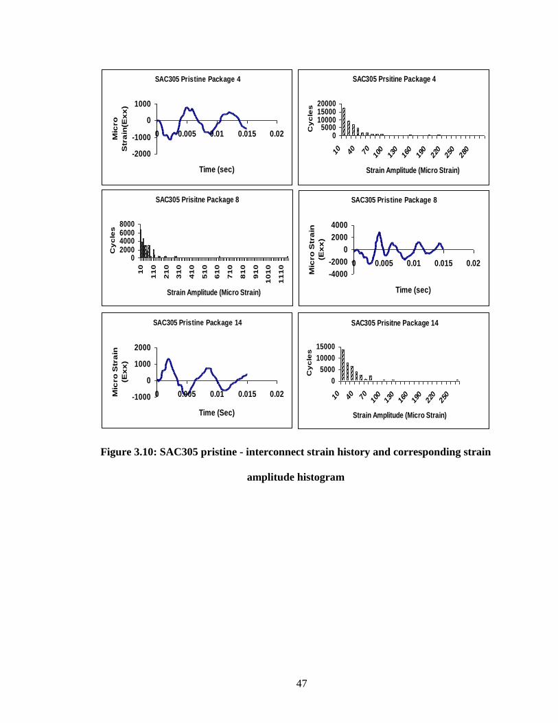
47
Figure 3.10: SAC305 pristine - interconnect strain history and corresponding strain
amplitude histogram
SAC305 Pristine Package 4
-2000
-1000
0
1000
0 0.005 0.01 0.015 0.02
Time (sec)
Mic
ro
Str
ain
(Ex
x)
SAC305 Prsitine Package 4
05000
100001500020000
10 40 70 100
130
160
190
220
250
280
Strain Amplitude (Micro Strain)
Cy
cle
s
SAC305 Pristine Package 8
-4000
-2000
0
2000
4000
0 0.005 0.01 0.015 0.02
Time (sec)
Mic
ro
Str
ain
(Ex
x)
SAC305 Prisitne Package 8
02000400060008000
10
11
0
21
0
31
0
41
0
51
0
61
0
71
0
81
0
91
0
10
10
11
10
Strain Amplitude (Micro Strain)
Cy
cle
s
SAC305 Pristine Package 14
-1000
0
1000
2000
0 0.005 0.01 0.015 0.02
Time (Sec)
Mic
ro
Str
ain
(Ex
x)
SAC305 Prisitne Package 14
0
5000
10000
15000
10 40 70 100
130
160
190
220
250
Strain Amplitude (Micro Strain)
Cy
cle
s

48
Figure 3.11: SAC305 thermally aged interconnect strain history and corresponding
strain amplitude histogram
Damage Superposition and Life Prediction based on Relative Damage Index
In this study, the test vehicles were subjected to JEDEC standard shock pulses.
Since the drops were highly repeatable, the corresponding solder interconnect strain
histories were also seen to be repeatable and hence damage was extrapolated to the point
of failure assuming linear superposition. The relationship between cumulative cycle
SAC305 Thermally aged Package 2
-15000
-10000
-5000
0
5000
10000
15000
0 0.005 0.01 0.015 0.02
Time (Sec)
Mic
ro S
train
(Exx)
SAC305 Thermally aged Package 2
0
1000
2000
3000
25
52
5
10
25
15
25
20
25
25
25
30
25
35
25
40
25
45
25
50
25
55
25
Strain Amplitude (Micro Strain)
Cy
cle
s
SAC305 Thermally aged Package 3
-1000
0
1000
2000
0 0.005 0.01 0.015 0.02
Time (Sec)
Mic
ro S
tra
in
(Ex
x)
SAC305 Thermally aged Package 3
0
5000
10000
15000
20000
25 75 125
175
225
275
325
375
425
475
525
Strain Amplitude (Micro Strain)C
ycle
s
SAC305 Thermally aged Package 7
-20000
0
20000
0 0.005 0.01 0.015 0.02
Time (Sec)
Mic
ro
Stra
in
(E
xx
)
SAC305 Thermally aged Package 7
0
5000
25
225
425
625
825
1025
1225
1425
1625
1825
2025
2225
Strain Amplitude (Micro Strain)
Cycle
s

49
counts till present drop and the damage accrued yet, as established previously in this
chapter is:
1
)2
(1
N
k nk
k
A
M
(3.30)
It should be noted that the if the cycles to failure (N) is known from dropping the
test vehicle to failure, the cumulative cycles to failure Mk can be related to the cumulative
solder interconnect strain amplitude Δε/2 by the coefficient „A‟ and the exponent „n‟.
This part of the study involves evaluation of these constants, hereby referred to as
Fatigue Constants. For determination of these constants, a non linear least square
minimizing algorithm known as the Levenberg-Marquardt Algorithm was used. Using
the interconnect strain data in the form of constant amplitude strain histograms from the
simulations and the failure data from the experimentation, initial guesses to the values of
„A‟ and ‟n‟ within a bounded space were given as inputs to the LM algorithm. The
algorithm then explored the bounded error space for global minima. The values of the
fatigue constants corresponding to the global minima were then used for the life
prediction model. A typical output from the LM algorithm showing the variation of error
in the multidimensional error space is shown in Figure 3.14.

50
Figure 3.12: 3d Error space - variation of error with ‘A’ and ‘n’
Levenberg-Marquardt Algorithm
In this study, the values of the constants „A‟ and „n‟ have been obtained which in
turn are used to predict the number of strain cycles and thereby the drops to failure. The
relation between the number of strain cycles to failure and the strain amplitudes is non
linear owing to the presence of the exponent „n‟. The optimization of the expression for
Relative Damage Index for computing the values of „A‟ and „n‟ is complex and involves
use of non-linear optimization techniques. The Levenberg Marquardt Algorithm has been
employed for the same.
Equation 3.30 can be expressed as f(p)=1 where p is the parameter vector
comprising of „A‟ and „n‟ pertaining to a particular interconnect type. For obtaining the
values of „A‟ and „n‟, the problem is formulated as a non linear least squares problem
whereby an initial parameter estimate p0 is provided and the squared error between the
Package 2
Error Space
Global Minima
‘A’ Value corresponding to minimum error
‘n’ Value corresponding to minimum error

51
desired and the obtained measurement vector is minimized. If ε =1-f(p) is the error and
g(p)= εTε is the squared error, the least square problem can be formulated as
[Minimize g(p) such that : p Є R ]
Here g(p) can be approximated by its Taylor series expansion as:
g(p+δp)= g(p) + g(p)T δp (3.31)
Where is the gradient operator. Now for the above approximation to be good, the
increment δp is to be chosen such as to minimize the error function ε =1-f(p).Then, the
minimizer parameter vector p, for the error function can be represented as
)()(2
1))((
2
1)( 2 pgpgpgpF T
i (3.32)
Where F(p) represents the objective function for minimizing the residuals gi .For
optimizing the objective function, the an initial parameter estimate p0 is provided and it is
desired to find the vector p’ that best satisfies the relation f(p)=1 while minimizing the
squared distance g(p).An iterative procedure for finding the global minima is adopted
.The iteration involves finding a descent direction „h‟ and a step length „α‟ which gives a
good decrease in the F value. The objective function for a small step length can therefore
be approximated by its Taylor expansion as:
F(p+αh)=F(p)+VhTF‟(p) (3.33)
If the function F(p+ αh) is seen to decrease, the function is said to be proceeding
in the descend direction „h‟. This implies that comparing F(p) with F(p+ αh) should give
hTF(p)<0.If no such h exists, then gradient F’(p) is zero, showing that the function is
stationary. The step length is obtained by a procedure called line search whereby the
distance from the current parameter vector p in the descent direction that brings about a

52
decrease in the objective function is quantified. The direction of steepest descent is
known to be in the direction of the negative gradient of error i.e along h= –F’(p).The
method in which the optimization is carried in this direction h=-F‟(p) is called the
Steepest Descent Method. This method performs well in steep regions where slow
convergence is advisable.
For shallow regions, where fast conversion is advisable, the Newton-Gauss
method works well. This method is based on the idea that non linear functions can be
approximated as linear functions based through Taylor expansion, as the error in the
system reaches a minimum. For a small ||δp||, a Taylor series expansion leads to the
approximation
hJ(p)g(p)h)g(p (3.34)
where J is the Jacobian Matrix. Substituting for g(p), in equation for F gives,
)()(2
1))((
2
1)(
1
2 pgpgpgpF Tm
i
i (3.35)
)h()h(2
1)h(L)hp(F T
(3.36)
hJJh2
1gJh)p(F)h(L
hJJh2
1gJhgg
2
1)h(L
TTTT
TTTTT
(3.37)
The gradient L is represented by,
hJJgJhL TT )(' (3.38)
When the gradient of a function is zero, it is known to be stationary. Therefore the
descent direction towards the region in error space where the error function becomes
stationary is given by

53
gJh)JJ( T
gn
T (3.39)
In each step, in the Gauss Newton method = 1 found by line search principle is used.
Levenberg Marquardt alternates between the steepest descent method and the
Gauss- Newton method depending on the proximity from the minimum in the error space.
In this method a positive constant referred to as damping is added to the diagonal of JTJ
to facilitate control over the convergence of the error function. The damping determines
the rapidness of the convergence, large damping implying slow convergence and vice
versa. A gain ratio parameter , is used for updating the iterations carried out by the LM
algorithm. Mathematically, is defined as
)gJh(h2
1
)px(F)x(F
)h(L)0(L
)hx(F)x(F
TT
(3.40)
A large gain ratio indicates that )p(L is a good approximation to )pp(F , and
there is a need for decrease in so that next LM step is closer to Gauss-Newton step. If
is small then, )p(L is a poor approximation and we should increase with the twofold
aim of getting closer to the steepest descent direction and reducing the step size. A
schematic diagram explaining the LM Algorithm is shown below.

54
Figure 3.13: Depiction of convergence of global minima in hybrid methods.
Evaluation of Fatigue Constants
Form the definition of cumulative damage index (equation 3.30) it can be seen
that for any particular interconnect type, if the fatigue constants “A” and “n” are known,
the number of cycles and thereby drops to failure can be predicted. The relationship
between these constants and the strain cycle amplitude and frequency is non-linear. Due
to this non-linearity, we have used the Levenberg-Marquardt Algorithm to evaluate “A”
and “n”. The algorithm has been modified to incorporate the equations relating the
fatigue constants and the strain parameters.
Error
Descent
Direction
Error from
Initial Guess
Gauss Newton Method
Steepest Gradient Descent Method

55
The constants „A‟ and „n‟ stand in the expression for Cumulative Damage Index
as:
1
)2
(1
N
k nk
k
A
M
Or f(A,n)=1 (3.41)
From the strain data pertaining to a particular interconnect in a package under
drop loading, the strain is converted from time domain to frequency domain using the
Rainflow Algorithm as explained above and a histogram is plotted. This data in
frequency domain is plugged in to equation 53 such that “k” is the bin-index for the
histogram, e/2 is the interconnect strain amplitude while N is the total number of bins in
the histogram and M is the total number of cycles in the kth
bin during all the drops until
failure. The two unknowns in the equation viz. the coefficient A and the exponent n are
computed by providing an initial guess to the values of A and n and carrying out
iterations as per the LM algorithm to explore the error space for a global minima. When
iterating close to the global minima, the method does a linear approximation through
Taylor expansion to the objective function in the neighborhood of the parameter to be
evaluated using. This requires the calculation of the Jacobian of the function with respect
to each unknown.
N
k
k
k
n
k
A
M
n
f
1
2log
2
(3.42)
N
k
k
n
k
A
M
A
f
12
2
(3.43)

56
Initial guess values to the parameter vector [A,n] were provided as input to the
Levenberg-Marquardt algorithm. The values were varied one at a time over a range
surrounding the expected values. The algorithm explores the error space by computing
minimized error for each value of the parameter vector. A schematic diagram explaining
the variation of A and n values is shown below.
Figure 3.14: Variation in initial guesses to the ‘A’ and ‘n’ values given as an input to
the algorithm.
The minimized errors are plotted against the corresponding „A‟ and „n‟ values
which gives 3-d plot of the error space as shown in the following figures.

57
Figure 3.15: Variation of ‘A’ and ‘n’ values across bounded error space and error
minimization.
Minimized
Error

58
Package 3
Package 8

59
Figure 3.16: Fatigue constants computation for pristine SAC105 interconnects based
on solder interconnect strain history using LM algorithm based error minimization.
Package 13

60
Package 2
Package 13

61
Figure 3.17: Fatigue constants computation for thermally aged SAC105 alloys based
on solder interconnect strain history using LM algorithm based error minimization.
Package 14

62
Package 1
Package 2

63
Figure 3.18: Fatigue Constants computation for pristine Sn3.5Ag interconnects
based on solder interconnect strain history using LM Algorithm based error
minimization.
Package 12
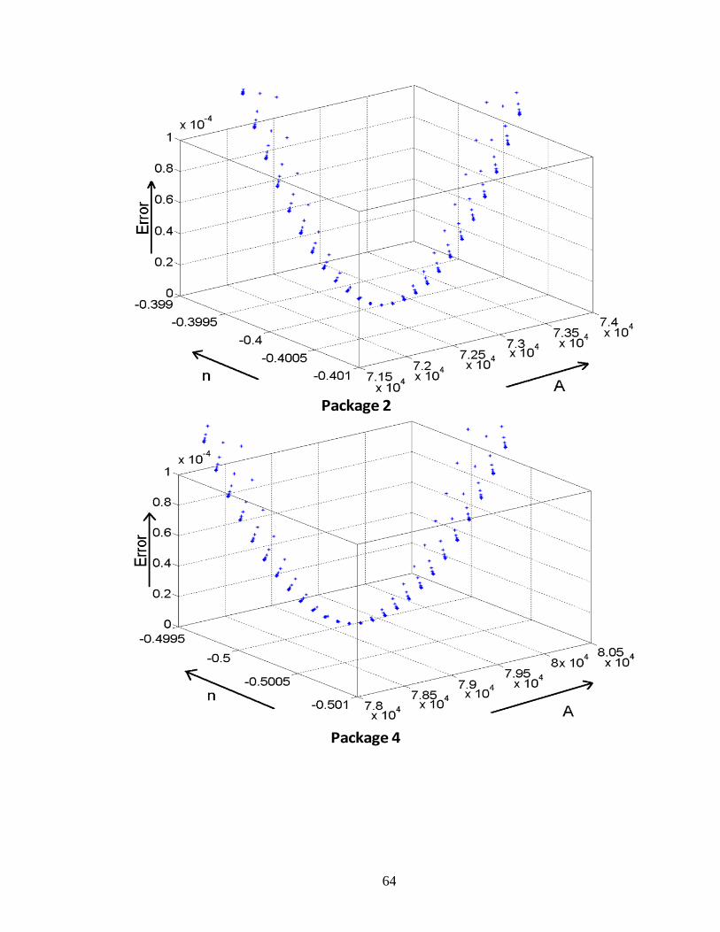
64
Package 2
Package 4

65
Figure 3.19: Fatigue constants computation for thermally aged Sn3.5Ag
interconnects based on solder interconnect strain history using LM algorithm based
error minimization.
Package 13

66
..
Package 4
Package 8

67
Figure 3.20: Fatigue constants computation for pristine SAC305 interconnects based
on solder interconnect strain history using LM algorithm based error minimization.
Package14

68
Package 2
Package 3

69
Figure 3.21: Fatigue constants computation for thermally aged SAC305 alloys based
on solder interconnect strain history using LM algorithm based error minimization.
3.4 Life Prediction of Lead-Free Alloy Based Solder Interconnects
The relative damage index established in this study has been used to predict the
number of drops to failure for both pristine and thermally aged solder interconnect alloys
subjected to drop test. Exposure to thermal aging reduces the number of drops to failure
for both experimental data and simulation. The proposed methodology enables evaluation
of the damage equivalency in the application of interest and for the packaging
interconnect query. Damage during the life of the product should not exceed “1” for the
design to have good survivability in drop and shock applications. The constants used for
damage progression are specific to solder alloy system. Table 3.2 shows the Fatigue
constants “A” and “n” developed using two methods. Model predictions and correlation
Package 7

70
with experimental data for SAC105, SAC305 and Sn3.5Ag Pristine and thermally aged
condition are also shown.
Table 3.2: Fatigue constants and life predictions
3.5 Failure Analysis and Effect of Thermal Aging on Drop/Shock Reliability
All the failed packages were cross-sectioned to investigate the failure modes.
Observed failure modes include, failure at the solder copper interface board side as well
as on component side and copper trace crack. The observed failures were predominant
across the interface of solder interconnect and copper pad on board side for thermally
aged samples of both the alloy system and in the case of pristine samples combination of
two or more failure modes were observed. The thermally aged solder interconnects were
observed to have lower drop and shock survivability as compared to pristine
interconnects. For both solder alloy system Weibull distribution exhibit different slopes
between pristine and thermally aged samples indicating the change in the failure modes.
Additionally the fatigue constants evaluated for all the cases correspond to the decreased
reliability of thermally aged interconnects. The „A‟ value was seen to decrease from
Actual Predicted
Failure Drop Failure Drop
SAC 105 Pristine 3.00 74700 -0.03 0.89 1065 1199 -12.63
8.00 78799 -0.02 78965 -0.04 0.84 1579 1872 -18.55
13.00 83395 -0.06 1.31 1622 1237 23.74
SAC 105 Thermally
Aged2.00 75200 -0.38 0.97 138 143 -3.32
13.00 74102 -0.33 1.18 226 191 15.33
14.00 74198 -0.40 0.84 120 143 -18.81
Sn3.5 Ag Pristine 1.00 75197 -0.28 0.94 172 183 -6.28
2.00 80793 -0.30 0.87 162 186 -14.73
12.00 83699 -0.25 1.21 233 192 17.44
Sn3.5 Ag Thermally
Aged2.00 72704 -0.40 1.36 114 84 26.29
4.00 79207 -0.50 0.86 66 77 -16.20
13.00 77202 -0.50 0.87 97 111 -14.78
SAC 305 Pristine 4.00 79899 -0.18 1.09 501 460 8.16
8.00 76701 -0.20 0.96 423 438 -3.64
14.00 81905 -0.23 0.95 165 174 -5.23
SAC 305 Thermally
Aged2.00 77095 -0.33 0.98 161 165 -2.29
3.00 83704 -0.43 0.74 163 220 -35.17
7.00 75694 -0.23 1.16 215 185 13.77
79502 -0.20
78831 -0.33
-0.37
76371 -0.47
74500
79896 -0.28
Avg n Computed RDI Error(%) Alloy Package A n Avg A

71
pristine to thermally aged conditions for all the three solder alloys compositions which is
in agreement with the failure data. Additionally, the exponent „n‟ was seen to increase in
the negative domain from pristine to thermally aged cases which correspond to a
decreased reliability after thermally aging as observed in the drop testing.
This chapter entails a life prediction model which facilitates reliability prediction
of solder interconnects without exhaustive testing. In this study Digital image correlation
(DIC) technique in conjunction with high speed imaging was been used to acquire full
filed strain, displacement and velocity components for lead-free board assemblies
subjected to impact. Obtained velocity components from experimental technique (DIC)
were transferred into finite element analysis as boundary conditions using node-based
submodeling approach to predict solder level strain history. Failure modes for the both
pristine and thermally aged lead-free alloys have been reported. Damage superposition
and life prediction model of the solder interconnect based on relative damage index has
been developed. Levenberg Marquardt Algorithm has been used to evaluate the fatigue
constants „A‟ and „n‟ which govern the life prediction model. Using these constants and
the strain data from a validated simulation, the life of the solder interconnects of the
assembly subjected to shock tests, can be predicted in terms of the number of shock
events to failure. The proposed model eliminated any need for exhaustive testing
procedures, significantly improving the product development cycle.

72
CHAPTER 4
BOARD TRACE FATIGUE MODELS AND DESIGN GUIDELINES FOR
ELECTRONICS UNDER SHOCK-IMPACT
4.1 Introduction
Driven by the trends towards miniaturization and increased functionality, modern
electronic systems are being built into more intricate and smaller packages. The
mechanical robustness of these smaller and more complex packages is of great concern to
the electronics industry. With advances in packaging technology, more reliable
interconnects are being designed as a result of which the accountability for failure shifts
to copper traces which form the primary failure mode. Previous researchers have
addressed copper trace fatigue reliability [Farley 2009] and existence of copper-trace
failures in drop-shock [Tee 2009]. This paper addresses the need for life prediction
models for PWB copper traces in shock and vibration environments. The study focuses
on low cycle fatigue of copper traces which is simulated by subjecting the PWB to cyclic
three point bending. Owing to the complexity of the test vehicle, global-local finite
element models were developed for simulating the board response. The study addresses
the need for empirical rules for trace layout on the PWB which ensure maximum
reliability. The effect of trace orientation, trace-pad fillet angle and trace width on its

73
reliability has been investigated. Using Digital Image Correlation based strain responses
and Finite Element Model based stress responses, mathematical models for damage
accumulation and life prediction of copper traces have been formulated and validated
with experimental failure statistics.
In applications ranging from handheld consumer products to military grade
mission critical equipment, reliability prediction of smaller and more intricate electronic
packaging configurations has been a challenge to researchers in the semiconductor
industry. Solder interconnects in CSPs and BGAs have been found by the researchers to
be the weakest link in the electronic assemblies, most susceptible to damage in harsh
environments. Previous researchers have studied second-level interconnects with focus
on design enhancement, fatigue modeling [Mattila 2004, Chai 2005, Lall 2006, tee 2004]
and life prediction [Lee 2000, Lall 2009, Luan 2005]. In presence of bending stresses due
to drop, shock and vibration, the copper traces on PCB surface experience high tensile
stress magnitudes. These stresses are often cyclic and result in failure due to fatigue in
terms of trace crack. Researchers [Tee 2008] have shown that improvements in solder
interconnect design has led to a shift in mode of failure from interconnect fracture to PCB
copper trace cracks. Previously, the effect of trace orientation [Tee 2009] and fatigue
behavior of copper traces in cyclic mechanical loading has been studied [Farley 2009].
However, life prediction of copper traces in shock and vibration is beyond the state of art.
This study focuses on detailed failure analysis of board traces subjected to high
magnitudes of cyclic mechanical loads with an objective of developing board design
guidelines and models for reliability prediction of copper traces subjected to mechanical
loads. Emphasis is laid on analysis of copper board trace failure analysis and

74
development of a fatigue model for their life prediction. Effects of trace orientation and
trace to pad dimensional ratio on its susceptibility to failure has been studied. Analysis of
board traces failure is done by integrating material characterization, experimental,
modeling techniques. Since the junction of traces and solder pads in electronic assemblies
are most likely to fail owing to the stress concentrations in these regions, this study
focuses on modeling and failure analysis of these regions of the assembly. Effect of
various pads to trace fillet angles as a function of their dimensional ratio has also been
studied. The effect of trace orientation on reliability has also been studied. Printed circuit
board assemblies without components have been tested to isolate the copper trace failure
and develop a mathematical model for life prediction of copper traces.
Figure 4.1 : Schematic diagram showing methodology adopted for development of
fatigue constants and evaluation of copper trace reliability
Test
BoardThree Point Bending
Strain Correlation With Global FE Models
Strain Data
Trace Fatigue by three point bending
Cycles to
Failure
FE Simulations
Strains at
failure locations
Strain Life Curve
cff
b
ff N2N2
E2
COPPER
TRACE
FATIGUE
MODEL

75
4.2 Test Vehicle
The test vehicle used for the study comprised of a JEDEC standard board without
any components on it. The 132mm X 77mm board has 9 traces running along its length
on either side. To study the effect of pad to trace dimensional ratio on its reliability, the 9
traces on either side were laid as combinations of 3 different pad and trace sizes. The
absence of components on the board helps in isolating copper trace cracks from other
failure modes that occur in interconnects and other parts of the component assembly.
Absence of second-level interconnects eliminates the possibility of the failure mode
involving copper trace delamination. The inclusion of traces laid out in a „zig-zag‟ pattern
enables an assessment of the effect of the various angles at which the traces merge with a
solder pad. Table 1 shows the pad and copper trace combination on the test vehicle. Pad
trace combinations have been studied to understand the effect of various trace
geometries.

76
Figure 4.2: Test vehicle schematic showing the location and layout of traces on both
sides of the board.
Top SideBottom Side

77
Table 4.1: Different pad/trace geometric combinations incorporated
in the test vehicle
Measurement of Circuit Board Deformation
In this study, the Digital Image Correlation technique was used to measure full
field strains on the surface of the Test Vehicle. The strain field measured using DIC was
to be subsequently used for validation of the FE Models developed as a part of the study.
Digital image correlation (DIC) is an optical method, used to measure full field
deformation and their derivatives on the surface of a loaded structure. DIC technique
involves application of speckle pattern on the surface of the structure with alternate mists
of black and white paints and tracking a geometric point on the speckle patterned surface

78
before and after loading and using it to compute both in-plane as well as out-of-plane
deformations in the structures.
Previously, Digital Image Correlation (DIC) has been used in the electronic
industry for various applications. DIC is used to measure full field displacement and
deformation gradient in electronic assemblies subjected to drop and shock [Lall 2007b,
2008a,b, Miller 2007, Park 2007, 2008], damping ratio on the surface of the board
[Peterson 2008] examination of velocity, rotation, bending on portable products subjected
to impact test [Scheijgrond 2005], stresses in solder interconnects of BGA packages
under thermal loading [Zhou 2001, Yogel 2001, Rajendra 2002, Shi 2004, Zhang 2004,
Zhang 2005, Xu 2006, Bieler 2006, Sun 2006], stresses and strain in flip-chip die under
thermal loading [Kehoe 2006] and warpage measurement on dual chip module [Ouimet
2008]. However, the application of DIC technique to study solder level deformation and
strain for transient event such as shock and drop of the PCB assembly has not been
completely explored. Behavior of the solder interconnects in printed circuit board
subjected to shock and drop is a major reliability issue in portable electronics.
In the Digital Image Correlation technique displacement field quantities are
obtained by tracking a geometric point before and after deformation [Zhou 2001, Amodio
2003, Srinivasan 2005, Kehoe 2006 and Lall 2007b, 2008a]. The tracking is achieved
using digital image processing of speckle pattern on the specimen surface. Figure 4.3
describes the basic principle of DIC.

79
Figure 4.3: 3D-Digital Image Correlation (DIC) principle
The sub image before impact is referred to as I1 (r) and the one after impact as I2
(r) respectively. The two are related as follows:
(3.1)
(3.2)
Where U(r) is the displacement vector at pixel r = (x, y, z)T . The difference in
the positions of the current pixel and the reference pixel gives the in-plane as well as out-
of-plane displacement U(r) of this reference pixel. Full-field displacement can thus be
found out by changing the reference pixel location on the speckle patterned surface and
following the same procedure described as above. A subimage around a reference pixel
„r‟ in the undeformed image is then compared with the subimages corresponding to
different pixels in the deformed image using a predefined correlation function. Difference
in the intensity of the two subimages is used to evaluate local translation of speckles.
Three typical correlation functions are defined as follows: [Zhou 2001]
)]r(Ur[I)r(I 12
)]r(Ur[I)r(I 21

80
Absolute difference:
dr)r(
dr)r()'rr(1)'r(
I
IIC
1
12
A
(3.3)
Least square:
dr)r(
dr)]r()'rr([1)'r(
2
1
2
12
L
I
IIC
(3.4)
and Cross-Correlation:
2/12
2
2
1
21
C
dr)'rr(dr)r(
dr)'rr(1)'r(
II
I)r(IC
(3.5)
where Ω (M x N) is the area of the sub-image around reference pixel r, r` is the current
pixel, CA(r`) is the current absolute correlation function, CL(r`) is the current least square
correlation function, and CC(r`) is the current cross-correlation function. The cross-
correlation functions provide the correspondence between matching subsets in images of
the un-deformed and deformed states. It is an iterative spatial-domain cross-correlation
method. This method maximizes the cross-correlation coefficient between a subset in the
reference image I1 and the deformed image I2.
4.3 Accelerated Testing
Stresses experienced by board traces caused due to drop and shock in actual
operating environment were simulated by subjecting the PCB to cyclic repetitive loading.
The experimental procedure involved determining overstress destruct limits of the PCB
and then performing accelerated tests at magnitudes well below the overstress limits. The
experimental setup involved a 3-point bending fixture used in conjunction with a
universal testing machine (Figure 4.4). The board was supported in two places,

81
symmetric about its center and subjected to prescribed out-of-plane deflection in the
center. Owing to the nature and symmetry of loading, it was expected that failure in the
traces would occur in tension, and therefore the traces on either side were subjected to
cyclic tensile stresses until failure. The test board was allowed to „roll‟ at the supports to
avoid membrane stress in the board. Strain data was acquired by placing strain gages at
six strategic locations on the board. The prescribed out of plane deflection was chosen
such that strains indicated by indicated by strategically placed strain gages were linear up
till their highest limits.
Figure 4.4: Schematic showing nature and direction of loading for accelerated
testing
The test vehicle was tested at different loading rates to investigate the effect of
rate of loading on modes of failure. The test vehicles were failed by subjecting them to
two different maximum cyclic stress levels to obtain different cyclic-life corresponding to
different stress levels in order to populate a „S-N curve describing the low cycle fatigue
behavior of the traces. This curve was further used in development of a power law
describing the fatigue life of the traces. Continuity across the traces was monitored using

82
a high speed data logger and failure data was obtained by recording the cycle counts at
which traces failed. Failed traces were then observed under a microscope for failure
analysis. It was observed that in all the cases the failure in traces occurred only at the
pad/trace joint. This is attributed to the stress concentrations at these locations due to the
discontinuities in geometry. The failure location on each trace was noted for comparison
with subsequent finite element analysis.
4.4 Finite Element Modeling
Owing to the complexity of the printed circuit board and in order to preserve the
geometrical details of the traces, a Global-Local sub modeling approach was used. Since
the failures observed during accelerated testing were localized in the trace/pad joints, sub
models preserving acute geometric details of these regions of the PCB were developed. A
defeatured global model of the PCB was created without copper trace architectural details
(Figure 4.5).Outputs from the global model were used to drive the local sub-models of all
the trace pad junctions on each trace.

83
Figure 4.5: Contour plot (global model) showing variation of longitudinal tensile
stresses on the PCB

84
Figure 4.6 Schematic describing the finite element modeling methodology used, with
implementation of global-local submodeling
DIC Based Full Field Strain
Global Model Simulation
Submodel Driven by
Global Model Results
Submodel Simulation used
for Failure Prediction
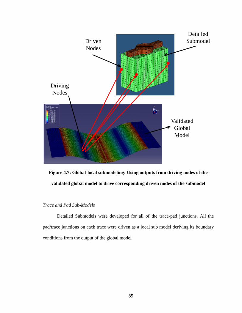
85
Figure 4.7: Global-local submodeling: Using outputs from driving nodes of the
validated global model to drive corresponding driven nodes of the submodel
Trace and Pad Sub-Models
Detailed Submodels were developed for all of the trace-pad junctions. All the
pad/trace junctions on each trace were driven as a local sub model deriving its boundary
conditions from the output of the global model.
Validated
Global
Model
Detailed
Submodel
Driving
Nodes
Driven
Nodes

86
Figure 4.8: Submodels for different straight pad-trace junction geometries
Figure 4.9: Sub models for different angled pad/trace junction geometries
Three categories of Submodels were made for each trace with a different
trace/pad dimensional ratio. 1) Nine submodels detailing the nine straight trace/pad
junctions with different trace/pad ratios (Figure 4.8); 2) Nine Submodels detailing the
nine angled pad/trace junctions with different trace/pad ratios (Figure 4.9); 3)
Trace - 1 Trace - 2 Trace - 3 Trace - 4
Trace - 5 Trace - 6 Trace - 8Trace - 7Trace - 5
Trace - 1 Trace - 2 Trace - 3 Trace - 4
Trace - 5 Trace - 6 Trace - 8Trace - 7Trace - 5

87
Multidirectional trace Submodels with traces routed from 0° to 315° at intervals of 45°
(Figure 4.10).
Figure 4.10: Multidirectional trace sub-models.
Model Validation
The finite element models developed for the trace-pad geometries were subjected
to boundary conditions representing a three point bending test with loading magnitudes
equal to the accelerated test parameters. The full field strain contours obtained from DIC
based measurements were compared with FE simulation prediction to validate the FE
model. A good correlation was obtained between the two.

88
Figure 4.11: Comparison of strains contours as obtained by DIC and as predicted
by FEA.
FE Simulation Predicted Strains

89
Additionally, a good correlation was achieved between areas of high stresses as
shown by the simulations and the actual failure locations (Figure 4.13 & Figure 4.14).
Figure 4.14 shows the correlation of model predictions with the failure locations.
Figure 4.12 : Variation of Longitudinal stresses along the length for different trace
geometries
Figure 4.13: Failure locations, as observed from FE simulations and accelerated
tests for straight traces
Variation of Stresses Along length of Board
0.00E+00
1.00E+08
2.00E+08
3.00E+08
4.00E+08
5.00E+08
6.00E+08
7.00E+08
8.00E+08
0 1 2 3 4 5 6
Trace Locations
Str
es
se
s (
Pa
)
Trace-1
Trace-2
Trace-3
Trace-4
Trace-5
Trace-6
Trace-7
Trace-8
Trace
Numbers
A1
A2
A3
B1
B2
B3
C1
C2
C3
Trace
Numbers
A1
A2
A3
B1
B2
B3
C1
C2
C3
Model Predictions
Observed Failure
Model Predictions
Observed Failure

90
Figure 4.14: Model predictions of stress concentrations and observed
locations of failure.

91
4.5 Trace Design Assessment
Effect of Trace/Pad ratio
Detailed failure analysis coupled with finite element simulations of the failed
regions showed a trend in the failure pattern which could be related to the geometries of
the trace/pad junctions. Stress levels in the trace-pad junctions were seen to decrease with
a decreased difference in trace width and pad diameter.
Figure 4.15: Comparison of peak strains in different trace/pad geometries.

92
Figure 4.16: Increasing stress concentration with increasing difference in trace
width and pad diameter.
For similar trace/pad ratio traces with bigger pads were seen to be more reliable
than those with smaller pads( Figure 4.15). The traces furthest away from fixed supports
Incre
asin
g D
iffere
nce in
Tra
ce
Wid
th a
nd
Pa
d D
ia
De
cre
asin
g L
on
gitu
din
al S
train
Le
ve
ls

93
were seen to fail first. The trace geometries correspond to the three trace groups shown in
Figure 9 and Table 1. A similar trend of increased strain with increase in (pad diameter,
d)/(trace width, w) is observed for all pad diameters.
Effect of Trace Orientation
From an assessment of the trace geometries tested, the traces with least trace/pad
ratio were seen to be most reliable. Multi directional trace models were developed for
these traces with traces routed from 0° to 315° at intervals of 45° (Figure 12).
Figure 4.17: Variation in maximum principal stress with angle made with
longitudinal direction of the board

94
Figure 4.18: Effect of trace orientation on max principal strain
The finite element simulations revealed a trend in the stress levels in traces
oriented at different angles. The traces which were laid at an angle closer to 0 and 180
degrees were seen to experience highest levels of stresses (Figure 13). The maximum
stresses in traces were seen to reduce as the angle approached 90°.
Effect of ‘Turning Angle’
From finite element simulations of the angled trace geometries, the effect of
„turning angle and its best possible orientation on a PCB was analyzed. It was observed
that irrespective of the trace width and the trace/pad ratio, maximum stresses occurred at
the fillet between the two traces, at the point where they met a pad.
0
0.001
0.002
0.003
0 45 90 135 180 225 270 315Ma
xim
um
Pri
nc
ipa
l Str
ain
Angle with length of the board
Effect of trace Angle on Maximum Principal Strain

95
Figure 4.19: A comparison of stress concentrations developed at the trace-pad
junctions for angled traces.
The longitudinal stresses in these traces produced a tearing effect at these
locations resulting in crack initiation at the fillets (Figure 4.19). Model predictions
indicate that sharp angles increased the strain concentration and obtuse turning angles
sustained lower strain concentrations.

96
Effect of Trace Routing Directions
In terms of the trace routing angle orientation, It was observed that if the traces
were routed in such at way that the trace „bends‟ opened up and closed under flexural
bending of the board, the stress concentrations produced were very high and resulted in
crack initiation at inner edges of the bend. It is suggested that the trace routing angles
should be made as obtuse as possible to avoid stress concentrations. Additionally, bends
in traces, should be placed such that they do not open up when the board is flexed as
indicated in the figure that follows.
Figure 4.20: Stress concentrations at sharp angles between traces.
Failure
Location
Failure
Location

97
Figure 4.21 : Figure showing optimum trace orientation for maximum reliability
Copper Trace Fatigue Failure Model
Combining the life distributions from experimental testing and stress magnitudes
at failure locations from the Finite element simulations, a relationship describing the
fatigue behavior of thin film copper traces was developed. A generalized strain life power
law is used to describe the fatigue failure of thin film copper traces. The strain data used
is derived from the full-field measurements and are subject to its accuracy. The durability
of the copper in PCB traces as observed from the study, can be described using a
generalized strain life power law given as:
cff
b
ff N2N2
E2
(4.6)
Where is the total strain range at failure location in a cycle, f and
f are the
failure stress and strains while Nf is the cycle count to failure. Owing to the nature of the
accelerated tests conducted, the failures incurred in the traces were due to low cycle
fatigue and therefore this equation can be reduced to:
B
f AN )( (4.7)
Longitudinal Direction Of Board
Reduced Strain
levels due to proper
trace orientation
High Strain levels
„tearing‟ effect
produced by board
flexure.

98
The fit values from experimental data are: A = 8.63 x 10⁻²⁷
and B = -12.195. The
relation between the strain life in terms of cycles to failure and the trace strain values can
be approximated by a log-log function. For the dataset obtained from the accelerated tests
and the finite element simulations, the best fit to the dataset was obtained by the function:
Figure 4.22: Fatigue curve describing the low cycle fatigue behavior of copper traces
4.6 Copper Trace Design Guidelines
Accelerated stress tests have been performed on a test vehicle having only copper
traces in order to isolate the copper trace failure modes. The effect of trace dimension,
trace/pad ratio and trace orientation on their reliability have been studied. The following
observations have been made
1. Failures in copper traces subjected to tensile stresses due to PCB bending in
drop and shock, are localized at pad/trace junctions. This can be attributed to
the stress concentrations at these locations sue to geometric discontinuities.
Cu Strain Vs Cycles to Failure
y = -0.0004Ln(x) + 0.0071
3.00E-03
3.50E-03
4.00E-03
4.50E-03
5.00E-03
100 1000Cycles to Failure (Nf)
Co
pp
er T
race
Str
ain
Cycles to Failure (Nf)

99
2. The traces with least difference in trace and pad dimensions are more reliable.
For traces with similar trace/pad dimensional ratio, wider traces and bigger
pads are seen to be more reliable.
3. The traces laid out on the PCB, at orientations parallel to the longitudinal
direction of the board, are least reliable when the PCB is subjected to bending
due to drop or vibration. The stress levels in the traces reduce and their
reliability increases as the angle of their orientation becomes closer to the
perpendicular to the length of the board.
4. The traces, when turned to conform to the circuit layout, should be turned at
as obtuse an angle as possible to prevent high stress concentrations. Also, the
turns should be oriented such that the flexing of the circuit board under action
of any shock/vibration does not cause the bend to open up or close.
Copper Trace Design guidelines
1. The traces should be made wider at the trace pad interfaces to minimize the
difference in trace/pad dimensional ratio. If the width if the traces are a
concern with regard to material consumption and trace density, the trace width
can be reduced after a certain distance from the trace/pad interface.
2. Since the trace failures were seen to occur mostly in exposed (regions not
covered by solder mask) regions of the trace, any discontinuities in the trace
dimensions in these regions should be avoided.
3. The traces should be laid out on the PCB at angles as close to 90° (w.r.t the
length of the board) as possible. If the layout of components on the PCB does

100
not support this, the traces should at least be routed from the pads at angles
close to 90° and oriented to lie in other directions, by turning the trace at
shallow angles.
In order to develop a mathematical model describing the fatigue behavior of the
traces, a Strain vs. cycles to failure curve has been populated from the results obtained
from accelerated stress tests. Fatigue Constants governing the linear-log function based
mathematical model characterizing the fatigue behavior of copper traces on PCBs
subjected to drop/shock or vibration have been developed. The model which can be
driven by strains predicted by finite element simulations can be used for assessment of
low cycle fatigue behavior of copper traces and their life prediction eliminating any need
for exhaustive testing procedures.

101
CHAPTER 5
RELIABILITY STUDIES ON PACKAGE-ON-PACKAGE COMPONENTS IN DROP
AND SHOCK ENVIRONMENTS
5.1 Introduction
The consumer electronics industry stands at a critical juncture where
manufacturers strive to incorporate more functionality in smaller packages. In the highly
competitive consumer electronics market, a continued demand for products with smallest
possible form-factor yet high functionality has led to the proliferation of 3D packaging
technologies. Package-on-Package (PoP) architectures, in particular have attracted a lot
of interest, especially in portable electronics industry. The advantages of these stacked
3D architectures include simplified and compact design, savings of board space allowing
for more package landings, reduced pin counts and optimized production costs.
While a lot of recent research, in the field of PoP architectures has been focused
on development of optimum process flows and warpage control during reflow, the effects
of reflow parameters on the quality of PoP build and the associated reflow defects(other
than warpage) have not been extensively researched. Additionally, the reliability issues
associated with PoP assemblies in drop and shock environments have largely been
neglected. Since PoP architectures find their applications mainly in portable electronics,
which are susceptible to frequent drops and careless handling at the hand of the

consumer, the reliability of PoP architectures in environments representative of
the real world is critical to their success in the industry.
In this study, Single component PoP test vehicles were fabricated as per JEDEC
standards for quantifying the reliability of PoP packages in drop and shock. Daisy
chained double-stack PoP components were used to identify failure for subsequent
drop/shock performance analysis. Experimental strain data acquired using Digital Image
Correlation and high speed continuity data- for identifying failure was used in
conjunction with validated FE simulations of drop test events; for assessment of
reliability of PoP architectures in drop/shock environments. Validated node based global-
local FE simulations were used to predict strains in critical solder balls in both layers of
the PoP stack. The drop/shock reliability studies and life prediction models presented in
this chapter, present an insight into PoP failures and eliminate the need for exhaustive
testing procedures.
5.2 Package-on-Package (PoP) Architecture
Driven by the trends towards miniaturization and increased functionality, the
electronics components used in consumer and industrial products are being made smaller
and more intricate. In order to achieve high functionality, more components are being
placed within smaller housings, which lead to exhaustion of XY space, leaving scope for
further population only in out-of-plane directions. The concept of stacking packages,
exploits this availability of space in z-direction to pack more functionality in smaller
form factors. In recent years, Package-on-Package assemblies, more commonly known as
PoP assemblies have gained wide acceptance, especially in the portable electronics
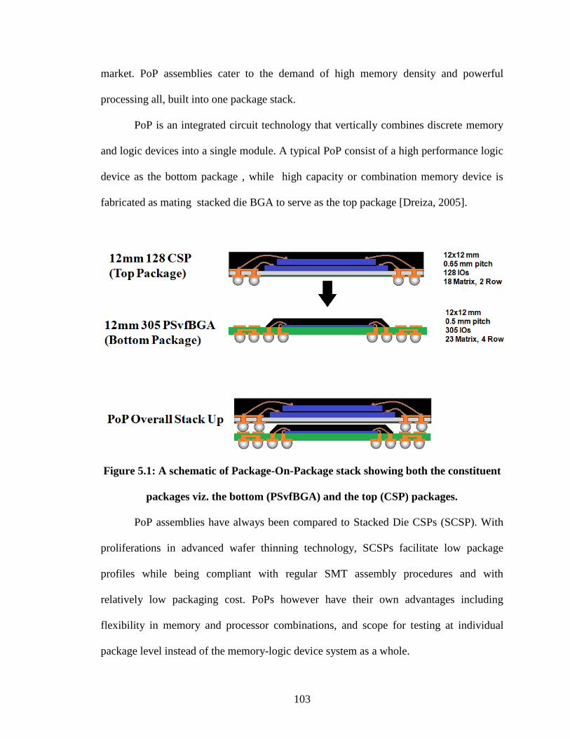
103
market. PoP assemblies cater to the demand of high memory density and powerful
processing all, built into one package stack.
PoP is an integrated circuit technology that vertically combines discrete memory
and logic devices into a single module. A typical PoP consist of a high performance logic
device as the bottom package , while high capacity or combination memory device is
fabricated as mating stacked die BGA to serve as the top package [Dreiza, 2005].
Figure 5.1: A schematic of Package-On-Package stack showing both the constituent
packages viz. the bottom (PSvfBGA) and the top (CSP) packages.
PoP assemblies have always been compared to Stacked Die CSPs (SCSP). With
proliferations in advanced wafer thinning technology, SCSPs facilitate low package
profiles while being compliant with regular SMT assembly procedures and with
relatively low packaging cost. PoPs however have their own advantages including
flexibility in memory and processor combinations, and scope for testing at individual
package level instead of the memory-logic device system as a whole.

104
While PoP architecture is gaining acceptance in electronics industry, low
assembly yield and reliability issues associated its their drop/shock and thermal
performances are of great concern to the manufacturers. In order for PoP assemblies to
proliferate throughout the packaging industry, there is an urging need for development of
standardized assembly processes which give good yields and reliable builds.
Additionally, with the development of technology, packages will be manufactured with
increased I/O counts and reduced pitch which would result in lower standoff height
between top and bottom packages- which further highlights the need for standardized
assembly processes and established reliability quantifications.
This study addresses the need for a standard assembly process and an insight into
board level reliability of PoP assemblies. This chapter validates a previously suggested
assembly process and suggests an optimum reflow profile for assembling PoP modules
while minimizing reflow defects. Furthermore, this part of the study aims at
quantification of board level reliability of PoP assemblies by performing JEDEC standard
tests followed by detailed failure analysis to isolate failures in mode and occurrence.
5.3 PoP Test Vehicle
For this study, a JEDEC standard test board was fabricated at NSF-CAVE3. The
test board made up of FR-4 had a single PoP assembly, populated on one side only. The
PoP stack fabricated, consisted of a 12mm X 12mm Package-Stackable-Very-Fine-Pitch
BGA (PSvfBGA) as the bottom package with another 12mm X 12mm CSP stacked on its
top. The bottom package (PvfBGA) had the solder balls arranged in a perimeter-array
configuration with an I/O count of 305, while the top package (CSP), also a perimeter

105
array package, had an I/O count of 128. The pitch between the solder balls was 0.5mm
for the bottom tier and 0.65mm for the top tier. Different solder alloys, representative of
the actual combinations used in the industry, were used in both top and bottom packages
for achieving extended reliability. The total height of the package stack was 1.2mm.
Figure 5.2: A schematic of Package-On-Package test vehicle developed, showing the
three different daisy chain channels and other board attributes.

106
Figure 5.3: Schematic describing test vehicle channels and other attributes
Figure 5.4: Single component JEDEC standard Package-on-Package test vehicle,
fabricated and used for the study.
A+,A- : Daisy Chain of PSvfBGA,
Bottom package balls
B+,B- : Daisy chain of top
junction (Top FBGA
to PSvfBGA 116 pin
memory interface)
C+,C- : Daisy chain of top
junction (Top FBGA
to PSvfBGA 12 corner
balls)
• Daisy chains for top junction
(top FBGA to PSvfBGA) routed from
„inside‟ package footprint via through-holes

107
Having a single component on the test vehicle, with the interconnects which are
being monitored for continuity, divided into several different daisy chains, facilitates
easier fault isolation for subsequent failure analysis. For this purpose, the solder balls in
the two tiers of the PoP stack were divided into three different daisy chains. The top tier
of solder balls between the bottom package (PSvfBGA) and the top package (CSP) was
divided into two different daisy chains- one connecting twelve corner solder balls, three
in each corner and the second connecting all the other solder balls. These two daisy
chains, connected to the copper pads on the PCB through two pairs of solder balls from
the bottom tier. The bottom tier of solder balls, between the package stack and the PCB
was included in a different daisy chain.
Figure 5.5: Schematic showing matching daisy chain net-lists on the top of the
bottom package (PSvfBGA) and the bottom of top package (CSP)
(Source: Amkor Technology)

108
Figure 5.6 : Schematic showing matching daisy chain net-lists on the bottom of the
bottom package (PsvfBGA) and the PCB
(Source: Amkor Technology)

109
Figure 5.7 : Schematics showing the classification of the two tiers of Solder
Interconnects into three daisy chain net-lists for the test component used in the
study (Source: Amkor Technology)
Daisy Chain netlist of PSvfBGA, Bottom
package balls
Daisy chain netlist of top junction (Top
FBGA to PSvfBGA 116 pin memory
interface)
Daisy Chain netlist of top side (Top FBGA to
PSvfBGA 12 corner balls)

110
Figure 5.8: Schematic of PoP stack with relevant dimensions.
Since SAC105 for Ni/Au finish and SAC125Ni for Cu OSP finish have been
highly recommended for applications requiring improved board level drop [Syed 2006];
SAC105 and SAC125Ni were used as solder for the balls on the top and bottom tiers of
the PoP stack, respectively. Additionally, SAC105 and SAC125Ni have been shown to
have better performance in board level drop tests as compared to SAC305 and SAC405
solder alloys and hence were preferred in the test vehicle.
5.4 PoP: Surface Mount Assembly
A regular BGA surface mount assembly process involves three basic steps- 1)
Stencil printing the solder paste on the PWB copper pads 2) placing the package on the
PWB while matching package footprint to the landing pads and 3) Reflow. While the
process has been well established and optimized for BGA assembly, it cannot be utilized

111
for Package on Package stacking without significant alterations. The factors which render
the regular BGA assembly process unsuitable for PoP assembly are as follows:
Firstly, the bottom package in a PoP assembly is generally of a very thin profile
which tends to induce a lot of warpage during reflow owing to CTE mismatch between
the laminate and the mold cap. Regular solder paste printing cannot efficiently address
the issue of warpage in the bottom package. In a regular screen printing process, the
thickness of the metal mask is of the order of 120um which owing to half of it being flux,
generates a solder paste deposition of around 60um thickness. Compared to a typical
bottom package warpage, which at its peak can be as much as about 100um, this
thickness of solder paste does not suffice to yield a good connection for all the solder
balls. On the other hand, if the thickness of the solder paste deposition is increased, it has
been shown[Yoshida,2006] that the surface tension from the large amount of the
transcribed solder results in pushing the substrate of the bottom package up during
reflow. Secondly, to enable lower stack profile, the bottom package is designed to have a
mold cap surrounded by copper pads on the substrate for receiving the solder balls from
the top package (CSP). This results in a non-level surface on the top of the bottom
package which renders it unsuitable for screen printing solder on the pads. Additionally,
it‟s necessary to supply adequate mount of flux and/or solder paste between the solder
balls from the top CSP and the copper pads on the bottom package to remove the oxide
film and achieve good connections.
Regular solder pastes, used for stencil printing applications have very high
viscosity which results in a lower transcription by dipping. For PoP assembly, novel
solder pastes have been developed which facilitate transfer of solder paste on to the

112
solder balls by dipping the packed in the solder paste. These novel PoP pastes, have
lower viscosity and smaller grain size [Takagi, 2005] which results in better „pick-up‟ of
paste after dipping.
Figure 5.9: A comparison between regular and PoP-specific solder paste, showing a
difference in amount of transcription achieved by dipping.
The solder dipping process, necessary for transcribing solder paste to the top tier
of solder balls, can also be extended for solder paste supply to the bottom tier of solder
balls. It has been shown that using solder paste dipping instead of screen printing for the
bottom package also, results in a better yield. For the PoP assembly used in this study,
the process flow was as follows:
1. Dipping the bottom package (PSvfBGA) into low-viscosity PoP solder paste
2. Placement of the bottom package on the PCB
3. Dipping the top package (CSP) into PoP solder paste
4. Placement of the top package (CSP) on the bottom package (PSvfBGA)
5. Reflow
Regular Solder Paste Solder Paste Designed
For PoP Assembly
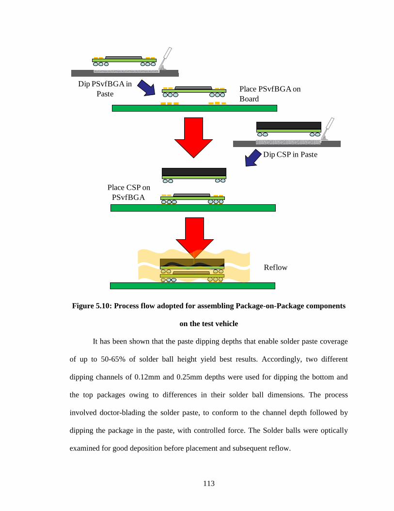
113
Figure 5.10: Process flow adopted for assembling Package-on-Package components
on the test vehicle
It has been shown that the paste dipping depths that enable solder paste coverage
of up to 50-65% of solder ball height yield best results. Accordingly, two different
dipping channels of 0.12mm and 0.25mm depths were used for dipping the bottom and
the top packages owing to differences in their solder ball dimensions. The process
involved doctor-blading the solder paste, to conform to the channel depth followed by
dipping the package in the paste, with controlled force. The Solder balls were optically
examined for good deposition before placement and subsequent reflow.
Dip PSvfBGA in
PastePlace PSvfBGA on
Board
Dip CSP in Paste
Place CSP on
PSvfBGA
Reflow

114
5.5 Reflow Parameters
Reflow Profile has a very important effect on the final yield of PoP assembly
process. In this study, various experiments were conducted to study the effect of reflow
profile parameters on PoP assembly. The defects that occurred as a result of
experimenting with the reflow profiles were analyzed for optimization of the reflow
profile. A major factor influencing the quality of the PoP build was warpage of the
package. The warpage during reflow at high temperatures, especially in the bottom
package, has been reported to be as large as 100um. A mismatch in the CTE of the
various components of the package viz. the die, the mold cap and the substrate, results in
a negative (concave) warpage of the bottom package and positive (convex) warpage of
the top package [Yim, 2010]. Additionally, the use of different solder alloys for
assembly, all of them Lead-free Compositions make it even more challenging to
accommodate reflow parameters that minimize warpage while staying within the narrow
reflow process window that is required to achieve optimum yield with lead-free alloys.
Figure 5.11: Mechanism of warpage due to CTE mismatch.
While the solder dipping procedure accommodates warpage due to reflow to an
extent, by supplying an adequate amount of solder paste/flux, large values of warpage,
still result in open connections. Owing to the geometry of the component, the warpage is

115
seen to be more severe in the bottom package, especially near the corner of the package.
As a result a lot of open connections were observed in the corner solder balls of the
bottom tier of I/Os.
Previously, researchers have outlined PoP stacking process flow for high yields
[Yoshida 2006, Dreiza 2006]; investigated the effects of material properties on PoP
package warpage behaviors [Yim, 2010] and developed models for warpage prediction in
PoP stacks during reflow. [Amagai, 2010]. However reflow defects, other than
associated with PoP assembly have largely been neglected. Variations to the reflow
profile parameters, suggested to account for warpage in the PoP constitutive packages
during reflow, often lead to other defects. Bound by the propensity of these defects, the
optimum profile window becomes very small. This study, aims at optimization of the PoP
reflow profile accounting for all the major reflow defects.
As a part of the study, different reflow profiles with varying Ramp Rates, Peak
Temperatures and Time-Above-Liquidus were used to reflow the assembly. Visual
inspection of the assembly following the reflow was performed to analyze the effects of
change in these reflow parameters on the yield of the process. The most common types
of defects observed during reflow are as follows:
1. Tombstoning: wherein one side of the package gets lifted up and the I/Os on
the other side solidify first, resulting in an improper package landing.
2. Open Joints, resulting from excessive warpage in the top and bottom package.
3. Bridging or Sliding of I/Os due to high peak temperatures.
4. Improper Reflow: Un-collapsed solder balls due to low peak temperatures of
less TAL.

116
5. Solder-Balling i.e. accumulation of tiny solder ball from the solder paste, non
the peripheral edge of the solder ball after reflow.
Figure 5.12: Solder reflow defect: Excessive warpage and tombstoning resulting in
open connections
Figure 5.13: Solder reflow defect: Improper reflow due to low peak temperature
and less TAL resulting in un-collapsed solder joints

117
Figure 5.14: Solder reflow defect: Bridging of interconnections leading to short-
circuits, resulting from high peak temperature and/or high TAL
Figure 5.15: Solder reflow defect : Head-in-Pillow defect resulting from premature
activation of flux due to high ramp rate and failure in removal of oxide film.

118
Figure 5.16: Solder reflow defect : Sliding of the package owing
to high warpage due to thermal shock
Figure 5.17: Good solder interconnections obtained by optimized reflow profile.
An optimized reflow profile was developed after a detailed analysis of the effects
of the aforementioned parameters on the quality of the build. The optimized reflow
profile had the following attributes:

119
1. A gentle Ramp-rate of about 1.5°C /min which was neither too high to result
in bridging, tombstoning or excessive package warpage nor too low to fail in
activating the flux in the solder paste and result in Solder-Balling or Head-in-
pillow type defects due to presence of oxide film
2. Ramp-to-Spike profile which unlike Ramp-Soak-spike profile does not
prematurely break down the flux activators in the solder paste, instead
preserves then throughout the preheat stage promoting better wetting.
3. Optimum Peak temperature of 255ºC which is well above the liquidus of the
solder alloys used (≈ 217ºC) but not too high to cause bridging or tombstoning
4. Optimum TAL of about 90 sec which is long enough for proper formation of
solder joint while not being too long to cause de-wetting and induce head-in-
pillow type defects.
Figure 5.18: Different reflow profiles adopted with different parameters. The
optimum profile (Profile-2) is highlighted in red.

120
Figure 5.19: Effect of reflow parameters on PoP assembly and induced defects.
5.6 PoP: Drop Testing
For evaluation of the Package-on-Package assembly reliability in shock, the test
vehicles were subjected to JEDEC standard drop, inducing a shock pulse of 1500G for
0.5ms. The continuity of all the three daisy chains were continuously monitored
throughout the drop event using high speed DAQ systems. The test boards were speckle
coated and the drop event recorded using High speed cameras for subsequent evaluation
of in-situ full field strain using Digital image Correlation technique.

121
Figure 5.20: Schematic of experimental set-up for controlled drop test with DIC
and DAQ systems
High Speed Cameras (10,000 fps)
Test Vehicle
Pulse Shaper
Drop Table
Drop Tower
DIC Setup
Hi-Speed Data Acquisition for Continuity Monitoring

122
Figure 5.21: Experimental set-up for controlled JEDEC drop test using
LANSMONT™ drop test tower.
Digital image correlation (DIC) is an optical method to measure full field
deformation and their derivatives i.e strain on the surface of a loaded structure. The
Digital Image Correlation technique involves application of speckle pattern on the
surface of the structure with alternate mists of black and white paints which are then
tracked as geometrical points during the monitored event, before and after loading and
using it to compute both in-plane as well as out-of-plane deformations in the
structures[Zhou 2001, Lall2007].

123
Figure 5.22: 3D-Digital Image Correlation- Basic principle [Panchagade, 2006]
High speed Data Acquisition systems were used to monitor the continuity of the
three daisy chains through the drop event, for detection of failure. Failure in the assembly
was defined as a peak in the resistance in any of the daisy chains which occurs as crack
propagates through an I/O resulting in an open connection. After performing drop tests on
the test-vehicle, until all the three daisy chains were rendered open the failed assemblies
were preserved for subsequent failure analysis failure analysis.
Previously it has been shown that small variation in drop orientation can produce
significantly varying transient-dynamic board responses. To avoid variations in drop
orientation, significant effort was made to establish repeatability of the drop event.

124
Figure 5.23: Strain repeatability through different shock events
To ensure repeatability of the drop event, strain histories, monitored using strain
gages mounted at key location on the test board and shock pulse measured using an
accelerometer were monitored for consistency.
5.7 Finite Element Models For Reliability Evaluation
Finite elements models were developed for simulating the drop/shock events and
evaluating the peak strain and stress values and the specific locations where they occur.
Owing to the complexity of the package on Package assembly and in order to preserve
the geometrical intricacies of the package stack in complete detail, a node based Global-
Local sub modeling approach was used. Since the failures observed during accelerated
drop testing were primarily seen to be localized in the corner solder balls, these I/Os were
modeled in complete detail while all the other Interconnects were modeled as
Timoshenko beam elements. A defeatured global model of the test vehicle was created
while using smeared properties for the PoP package stack. The outputs from the global
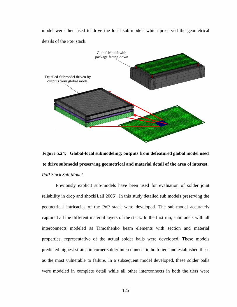
125
model were then used to drive the local sub-models which preserved the geometrical
details of the PoP stack.
Figure 5.24: Global-local submodeling: outputs from defeatured global model used
to drive submodel preserving geometrical and material detail of the area of interest.
PoP Stack Sub-Model
Previously explicit sub-models have been used for evaluation of solder joint
reliability in drop and shock[Lall 2006]. In this study detailed sub models preserving the
geometrical intricacies of the PoP stack were developed. The sub-model accurately
captured all the different material layers of the stack. In the first run, submodels with all
interconnects modeled as Timoshenko beam elements with section and material
properties, representative of the actual solder balls were developed. These models
predicted highest strains in corner solder interconnects in both tiers and established these
as the most vulnerable to failure. In a subsequent model developed, these solder balls
were modeled in complete detail while all other interconnects in both the tiers were
Global Model with
package facing down
Detailed Submodel driven by
outputs from global model

126
modeled as Timoshenko beams. Owing the as mismatch in the solder ball dimensions and
pitch between interconnects in both the layers, the modeling of the PoP stack was found
to be very challenging.
Figure 5.25:Detailed submodel preserving the geometrical detail and various
material layers of the PoP stack with the corner solder balls modeled in detail while
all other I/Os are modeled as Timoshenko beam elements.
PoP Assembly Schematic

127
Figure 5.26: PoP assembly submodel- critical corner interconnect
Table 5.1:PoP submodel: Elements and material properties used
Model Validation
The full-field filed quantity values on the surface of the PoP test vehicle from DIC
based measurements were correlated with those obtained by Finite Element Method
based simulations, to validate the accuracy of the model in predicting the stress and strain
Top Package Mold
Encapsulant
Top Solder Ball
Bottom Package
Substrate
Bottom Solder ball
PCB
ComponentElement
Types
Material Properties
DensityElastic
ModulusPoisson's
Ratio
PCBS4R,
C3D8R1819.5694 1.60E+10 0.33
Substrate C3D8R 1400 2.41E+10 0.3
Mold Compound
C3D8R 1970 1.55E+10 0.25
Corner Solder Interconnects
C3D8R
7346 4.70E+10 0.35Remaining Solder
InterconnectsB31

128
values in the PoP assembly. Figure 22 shows a comparison of z-displacement as
measured experimentally and as predicted by FE simulations on the surface of the PCB.
Figure 5.27: Figure showing correlation between DIC and FE simulation based
strain contours on the test vehicle surface- incurred during drop event.

129
Figure 5.28: A comparison of out of plane displacements as evaluated by DIC and
predicted by FE simulations
T=0.75 ms after impact
T=3.5 ms after impact
T=5.25 ms after impact
T=13 ms after impact

130
Additionally, strain gages were mounted at critical locations on the test board.
Strain histories from the strain gage were used to validate the global-model by comparing
them to strain histories predicted by FE simulation at the same location.
A good correlation between filed quantity (displacement) and derivatives of field
quantity (strain) values from experimental observations and FE simulations was obtained
which validates the accuracy of the model (Figure 22). The model was then be used drive
the detailed global local submodels and predict stress/strain peaks and the locations
where they occur in high magnitude or concentration.
Model Predictions
The validated FE model simulations were used to predict failure modes and
locations. A preliminary simulation with all the interconnects modeled as Timoshenko
beam elements with representative section properties showed that the corner
interconnects in both the tiers of I/Os to incurred highest levels of stresses, hence these
interconnects were modeled in complete detail in subsequent modeling iteration.
Strain histories at the critical corner interconnects were extracted for both the
tiers of solder balls. A comparison of strain histories at the four corners of the PoP stack
showed a diagonal-symmetry in the strain responses. The interconnects in the top left and
bottom right corner were seen to experience similar strain cycles as were the
interconnects in the top right and bottom left corners of the PoP stack.

131
Figure 5.29: Strain histories extracted at the four corner interconnects in the bottom
tier of solder balls.
Figure 5.30: Strain histories extracted at the four corner interconnects in the top
tier of solder balls.
The FE simulations also showed that the strains induced were substantially higher
in bottom tier of solder balls as compared to the top tier. As a result, the corner I/Os in
12
3 4DROP
-0.001
-0.0008
-0.0006
-0.0004
-0.0002
0
0.0002
0.0004
0.0006
0.0008
0 0.001 0.002 0.003 0.004 0.005 0.006Stra
in
Time (Sec)
Strain Histories at Four Corner Interconnects(Bottom Tier)
Corner-1 Corner-2 Corner-3 Corner-4
-0.0006
-0.0004
-0.0002
0
0.0002
0.0004
0.0006
0 0.001 0.002 0.003 0.004 0.005 0.006
Stra
in
Time (Sec)
Strain Histories at Four Corner Interconnects(Top Tier)
Corner-1 Corner-2 Corner-3 Corner-4
12
3 4DROP

132
the bottom tier, i.e. the interconnects between the bottom package(PSvfBGA) and the
PCB were expected to fail first.
Figure 5.31: A comparison of strain cycles experienced by solder interconnects in
the top and bottom tiers located at corner-1 as shown in schematic
Figure 5.32: A comparison of strain cycles experienced by solder interconnects in
the top and bottom tiers located at the corner-2 as shown in the schematic
-0.001
-0.0008
-0.0006
-0.0004
-0.0002
0
0.0002
0.0004
0.0006
0.0008
0 0.001 0.002 0.003 0.004 0.005 0.006Stra
in
Time (Sec)
Strain Histories for Interconnects at Corner-1
Bottom Interconnect Top Interconnect
12
3 4DROP
-0.001
-0.0008
-0.0006
-0.0004
-0.0002
0
0.0002
0.0004
0.0006
0.0008
-0.001 6E-18 0.001 0.002 0.003 0.004 0.005 0.006Stra
in
Time (Sec)
Strain Histories for Interconnects at Corner-2
Bottom Interconnect Top Interconnect
12
3 4DROP

133
Figure 5.33: A comparison of maximum and minimum out of plane strains
experienced by corner solder interconnects in the bottom tier.
Figure 5.34: A comparison of maximum and minimum out of plane strains
experienced by corner solder interconnects in the top tier.
-1000
-800
-600
-400
-200
0
200
400
600
800
Corner-1 Corner-2 Corner-4 Corner-3Stra
in(M
icro
stra
ins)
Max and Min Z-Strains in Four corner Interconnects -Bottom Tier
Max Strain
Min Strain
12
3 4DROP
-500
-400
-300
-200
-100
0
100
200
300
400
Corner-1 Corner-2 Corner-4 Corner-3Stra
in(M
icro
stra
ins)
Max and Min Z-Strains in Four corner Interconnects -Top Tier
Max Strain
Min Strain
12
3 4DROP

134
Additionally, in both the tiers of solder balls, the stresses were seen to be higher
towards the bottom (solder ball to substrate/PCB) side. This indicates a high probability
of crack development in the interface between solder ball and copper pad at the PCB side.
Figure 5.35: Stress Distribution in the critical corner interconnect at different time
steps during shock event.
Time = 0.0006 Sec
Time = 0.0030 Sec Time = 0.0036 Sec
Time = 0.0024 SecTime = 0.0018 Sec
Time = 0.0012 Sec

135
5.8 PoP Vs BGA: Susceptibility to failure
In order to compare the reliability of PoP Stacks with BGAs of similar
dimensions, a separate submodel representing a BGA with same dimensions and weight
as the PoP stack was developed. The stresses in the bottom tier of interconnects from the
PoP stack were compared to those induced in a regular BGA interconnects. The FE
simulations of both the package types subjected to a similar shock pulse predicted that the
stresses in the bottom tier of interconnects of the PoP stack were higher in magnitude as
compared to those induced in the BGA interconnects. Figure 31 shows a comparison of
the stress in the dropping direction, in the corner interconnects, which were modeled in
complete detail in both the submodels.
Figure 5.36: A comparison of stresses induced in a corner interconnect for
Package-on-Package and BGA packages
PoP BGA

136
In order to gauge their susceptibly to cratering/copper pad delamination, the out-
of-plane stresses in the PCB side copper pads were compared between the PoP stack and
a regular BGA.
Figure 5.37: A comparison of out-of-plane stresses induced in corner PCB side
copper pads interconnect for PoP and BGA packages
The copper pads for the PoP stacks were seen to experience higher stresses than
those corresponding to a regular BGA. However with the alloy composition used in this
study, no cratering or copper pad delamination type of failures were observed.
5.9 Failure Analysis
After failures was observed as peaks in resistance across a daisy chain in the
assembly, the package stack was potted in epoxy and polished for identification of crack
location, by visual inspection under a Microscope.
PoP BGA

137
In accordance with the FE model predictions, a majority of the failures were seen
to occur in the bottom tier of solder balls. The three daisy chains that separated the top
tier of interconnect from the bottom tier, facilitated easier isolation of failure. In
agreement with the FE model predictions, the bottom tier of solder interconnect were
seen to fail first. Since the daisy chain connecting the top tier of solder interconnects
communicated with the pads on the PCB through two pairs of I/Os in the bottom tier,
these I/Os were inspected for failure to make sure the open event was not due to failures
in these connecting interconnects.
Figure 5.38: Figures showing failure locations as observed by cross sectioning and as
predicted by FE simulations

138
Additionally, cracks observed in the corner solder balls established them as the
most susceptible to failure. The observed Failure locations were compared with locations
where the FE simulations predicted occurrence of high stresses. A good correlation was
observed between the experimentally observed and predicted failure locations.
Conclusively, in this study a JEDEC standard single component test vehicle was
fabricated for evaluation of Package on Package reliability in drop/Shock environments.
It was observed that selection of Solder Paste and reflow profile parameters play a very
crucial role in the yield of PoP assembly process. The process flow suggested by previous
researchers, wherein solder dipping for both the tiers of solder balls, is advocated has
been further validates in this study. Additionally, an optimum reflow profile obtained by
detailed analysis of the effects of profile parameters on induced reflow defects has been
suggested. The suggested reflow profile has the following attributes:
1. Ramp-to-Spike profile, instead of Ramp-Soak-Spike profile to avoid
premature flux activation
2. Gentle ramp rate to allow for timely flux activation and adequate wetting and
dissolution of oxide film preventing proper solder connections and avoid
thermal shock to the components.
3. A for allowing moderate peak temperature well above the liquidus of the
solder used, but low enough to avoid excessive warpage
4. An optimum TAL ob about 60-90 seconds to facilitate proper reflow without
defects.
Additionally, validated finite element simulations were used to predict failure
locations in PoP assemblies. A detailed analysis of the strains experienced by the two

139
tiers of interconnects was performed. A comparison of the strain cycles experienced by
the corner interconnects in the two tiers, established that the corner interconnects in the
bottom tier of I/Os was the most susceptible to failure. Cross sections of failed PoP
stacked validated the FE model based predictions, in that, no failures were observed in
the top tier of interconnects and the cracks observed in the bottom tier were localized to
the corner interconnects.
In order to compare their reliability with BGAs, , a comparison of the stresses
incurred in the bottom tier of interconnects of a the PoP stack with those induced in the
interconnects of a BGA of similar attributes was made.
The PoP assembly processes and reflow parameters suggested in this study can be
used for achieving a high-yield of PoP assembly. Furthermore, the validated FE models
developed can be used to evaluate effects of design iterations in PoP assemblies
eliminating the need for exhaustive testing.

140
CHAPTER 6
SUMMARY AND CONCLUSIONS
The motivation behind this study is derived from the need for life prediction
models for electronics in drop and shock. With packaging technology evolving at
unprecedented rates, the product development cycles are shortened to meet the demands
of the highly competitive market. This work, addresses the issue by demonstrating the
feasibility of FE modeling for performing efficient reliability studies. Additionally,
presented in this work, are life prediction models for leadfree BGA solder interconnects
and PCB surface copper traces. These models, developed from validated FE model
outputs and actual testing data, eliminate the need for exhaustive testing procedures.
Using these models, the effects of various design iterations on the life of interconnects
and copper traces in assemblies subjected to drop/shock can be analyzed without testing
each design variation. The technique heavily relies on the accuracy of the Finite Element
models developed to represent the assembly subjected to mechanical loading. It is
therefore of outmost important that the techniques presented in this study be used with
caution and a thorough understanding of the design variables.
Chapter 3 presents a mathematical model which relates the life of BGA
interconnects in terms of shock-events-to-failure, to the strain levels experienced during a
single drop event; through a set of constants referred to as fatigue constants. The values

141
for these constants were seen to vary between solder alloy compositions and also
with thermal aging of the components. The variation in the constant values between
thermally aged and pristine interconnects, correlated well with the degrading effect
thermal aging had on the reliability of the interconnect. It should be noted that the values
of fatigue constants presented in this work are for Pristine and a single thermal aging
condition only. The values governing the model cannot be used for assemblies thermally
aged at different temperatures and for different durations; without substantial error in the
predicted life. For pristine assemblies however, the constants developed in this work can
be used with the error in predicted life well within experimental bounds.
The life prediction model developed in this work, relies heavily on the accuracy
of the FE model that the strain history for the interconnect is extracted from. It is
therefore important to make sure that the FE simulation of the shock event is correlated
with experimental results. With a validated FE model, the strain histories extracted at the
critical solder interconnects can be used as an input to the life prediction model. Minor
design variations can be incorporated in the FE model and the output from the simulation
can again be used in conjunction with the Life Prediction model to see its effect on the
life of the interconnects. The life prediction model and methodology presented in this
chapter, eliminate the need for exhaustive testing of each design variation and equip the
component designer with a powerful tool to evaluate components designs in terms of
reliability. While this study presents life prediction models for sequential thermal aging
and drop, future studies could address assemblies which undergo simultaneous thermally
aging and shock induced mechanical loading.

142
The study on cupper traces aimed at evaluating the reliability of PCB surface
copper traces. The study set forth a set of empirical guidelines which summarize the
effects of trace geometries and orientation on their drop/shock reliability. The design
guidelines provide a PCB designer with a set of rules that he can follow to ensure highly
reliable copper traces-without a detailed knowledge of their failure mechanisms.
Additionally, the study presents a mathematical model, which can be used to evaluate the
fatigue life of copper traces on the PCB surface.
It would be interesting to perform similar studies on copper traces embedded
between different layers of a composite PCB. While the fatigue model presented in this
study is valid for low cycle fatigue, a similar model which covers high cycle fatigue can
also be developed. In conjunction, the two models could be used for life prediction of
cupper traces in subjected to high g-level shock pulses, be decomposing the strains
experienced by the traces into constituent cycles of constant algorithm, as was done for
the BGA interconnects in Chapter 3. While the study addresses the need for empirical
design guidelines for ensuring Cu-trace reliability, a life prediction model for the same
would also aid the cupper trace design process.
The study on novel Package-on-Package architecture addresses the issues
involved with manufacturing these components. IN the study, a JEDEC standard single
component test vehicle was fabricated for evaluation of Package on Package reliability in
drop/Shock environments. The effects of Solder Paste attributes and reflow profile
parameters on the yield of PoP assembly process were studies. Additionally, an optimum
reflow profile obtained by detailed analysis of the effects of profile parameters on
induced reflow defects was suggested. The study further used , validated finite element

143
simulations to predict failure locations in PoP assemblies by performing a detailed
analysis of the strains experienced by the two tiers of interconnects.
A comparison of the strain cycles experienced by the corner interconnects in the
two tiers, established that the corner interconnects in the bottom tier of I/Os was the most
susceptible to failure. Cross sections of failed PoP stacked validated the FE model based
predictions, in that, no failures were observed in the top tier of interconnects and the
cracks observed in the bottom tier were localized to the corner interconnects. In
conclusion, a comparison of the stresses incurred in the bottom tier of interconnects of a
PoP stack with those induced in the interconnects of a BGA of similar attributes was
made with an intention of comparing the two in terms of their drop/shock reliability.
In conclusion, this study presents life prediction models, suggests optimum
manufacturing processes and design guidelines which aid in design and fabrication of
reliable electronic components, within the constraints of short product development
cycles.

144
BIBLIOGRAPHY
Abaqus 6.9-1 Documentation 2009
Abdulhamid, M., Basaran, C., “Influence of thermomigration on lead-free solder joint
mechanical properties”, Journal of Electronic Packaging 131:011002, 2009.
Abdul-Baqi, A., Schreurs, P. J. G., Geers, M. G. D., “Fatigue damage modeling in solder
interconnects using a cohesive zone approach”, International Journal of Solids and
Structures, Volume 42, pp. 927-942, 2005.
Amagai, M., Suzuki, Y., A study of package warpage for package on package (PoP),
Electronic Components and Technology Conference (ECTC), 2010 Proceedings 60th ,
vol., no., pp.226-233, 1-4 June 2010
American Society of Mechanical Engineers (ASME), “Standard Practices for Cycle
Counting in Fatigue Analysis”, ASTM E1049-85, 1997
Amodio, D., Broggiato, G., Campana, F., Newaz, G., Digital Speckle Correlation for
Strain Measurement by Image Analysis, Experimental Mechanics, Vol. 43, No.4, pp.
396-402, 2003.
Bannantine, J. A., Comer, J.J., Handrock, J.L., “Fundamentals of Metal Fatigue
Analysis”, Prentice Hall, 1990.
Bhate, D., Chan, D., Subbarayan, L., Nguyen, L., Fatigue Crack Growth and Life
Descriptions of Sn3.8Ag0.7Cu Solder Joints: A Computational and Experimental Study,
Proceedings of the 57th Electronic Components and Technology Conference, pp. 558-
565, 2007.
Bieler, T., Jiang, H., Influence of Sn Grain Size and Orientation on the
Thermomechanical Response and Reliability of Pb-free Solder Joints, Proceedings of the
56th ECTC, pp. 1462- 1471, May 2006.
Chai, T.C., Quek, S., Hnin, W.Y., Wong, E.H., Chia, J., Wang, Y.Y., Tan, Y.M., Lim,
C.T., Board Level Drop Test Reliability of IC Packages, Electronic Components and
Technology Conference, pp. 630-636, June, 2005

145
Che, F.X., Luan, J.E., Baraton, X., Effect of silver Content and Nickel Dopant on
Mechanical Properties of Sn-Ag-based Solders, Proceedings of the 58th ECTC, Orlando,
Florida, pp.485-490, May27th-May30th, 2008.
Chen, K. M., Ho1, K. K., Jiang, D. S., Impact Of Lead Free Solder Materials On Board
Level Reliability For Low-K Wlcsp, International Microsystems, Packaging, Assembly
and Circuits Technology, pp. 243-245, 2007.
Choi, J.Y., Kang, I.S., Park, B.J., Park, Y. M., Jung, G.J., Study on Inter-Metallic
Compound (IMC) at Interface of Pb-Free Solder and Nickel UBM for Mobile
Application, Proceedings of the 57th ECTC, Reno, Nevada, pp.1802-1808, May29th-
June 1st, 2007.
Chong, D.Y.R., Toh, H.J., Lim, B.K., Low, P. T.H., Drop Reliability Performance
Assessment for PCB Assemblies of Chip Scale Packages (CSP), Electronic Packaging
Technology Conference, pp. 262-269, June, 2005.
Cook, R.D., “Concepts and Applications of Finite Element Analysis” John Wiley &
Sons, NY, 1981.
Cote, K.J.; Dadkhah, M.S., Whole field displacement measurement technique using
speckle interferometry, Electronic, Proceedings of the 51st Electronic Component &
Technology Conference, pp.: 80-84, 29 May-1 June 2001.
Davis, C., Freeman, D., Statistics of subpixel registration algorithms based on
spatiotemporal gradients or block matching, Optical Engineering, Vol. 37, pp. 1290-
1298, 1998.
Downing, S. D., and Socie, D. F., “Simple Rainflow Counting Algorithms, International
Journal of Fatigue”, Vol. 4, No. 1, pp. 31-40, 1982.
Dreiza, M., et al., Stacked Package-on-Package Design Guidelines , International Wafer
Level Packaging conference, 2005.
Dreiza, M., L. Smith, G. Dunn, N. Vijayaragavan, J. Werner, Package on Package (PoP)
Stacking and Board Level Reliability: Results of Joint Industry Study, Proceedings of
IMAPS 2006.
Eslampour, H., Lee, S., Park, S., Lee, T., Yoon, I., Kim, Y., Comparison of Advanced
PoP Package Configurations, 60th Electronic Components and Technology Conference
(ECTC), Las Vegas, Nevada, pp. 1946 – 1950, June 1-4, 2010
European Directive 2002/95/EC, Restriction on the use of hazardous substances in
electrical and electronical equipment.

146
Gu, J., Cooreman, S., et al., Full-Field Optical Measurement For Material Parameter
Identification With Inverse Methods, WIT Transactions on The Built Environment, Vol.
85, 2006.
Gu, J., Lim, C., Tay, A., Equivalent solder joint and equivalent layer models for the
simulation of solder column failure under drop impact, Proceedings of 6th Electronics
Packaging Technology Conference, pp. 547–552, 2004.
Gu, J., Lim, C., Tay, A., Simulation of mechanical response of solder joints under drop
impact using equivalent layer models,” in Proceeding of 55th Electronic Component
Technology Conference, Orlando Florida, pp. 522–529, May31 -June 3, 2005.
Helm, J., McNeill, S., Sutton, M., Improved Three- Dimensional Image Correlation For
Surface Displacement Measurement, Society of Photo-Optical Instrumentation
Engineers, Vol. 35, No. 7, pp. 1911-1920, July 1996.
Ho, H.M., Oh, K.E., Wong, E.H., Lim, T.B., Application of moire interferometry in
electronics packaging, Proceedings of the Electronic Packaging Technology Conference,
pp. 277 – 282, 1997.
Huang, B., Hwang, H., Lee, N., A Compliant and Creep resistant SAC-Al(Ni) Alloy,
Proceedings of the 57th ECTC, Reno, Nevada, pp. 184- 191, May 29-June 1, 2007
Irving, S., Liu, Y., Free Drop Test Simulation for Portable IC Package by Implicit
Transient Dynamics FEM, 54th Electronic Components and Technology Conference, pp.
1062 – 1066, 2004.
Iyer, G., Ouyang, E., Kittidacha, W., Tantideeravit, S., Suresh, L.K., Pb-free Solder:
SAC105 vs SAC305 Drop-Test Reliability Data Comparison, International Electronics
Manufacturing Technology Symposium, pp. 251-255, 2007.
Jang. J., De Silva, A.P.,Drye, J.E., Post, S. L., Owens, N.L., Lin, J., Frear, D.R., Failure
Morphology After Drop Impact Test of Ball Grid Array (BGA) Package With Lead-Free
Sn–3.8Ag–0.7Cu and Eutectic SnPb Solders, IEEE Transactions On Electronics
Packaging Manufacturing, Volume:30, Issue 1, pp. 49 – 53, January, 2007.
JEDEC Standard JESD22-B111, Board Level Drop Test Method of Components for
Handheld Electronic Products, 2003.
Jie, G., Lim, C.T., Tay, A.A.O., Equivalent Solder Joint and Equivalent Layer Models for
the Simulation of Solder Column Failure under Drop Impact, Electronic Packaging
Technology Conference, pp. 547-552, June, 2004.
Johnson, M., E., Lu, H., Y., Lawhead, D., Tessier, T., Scott, D., Curtis, A., Using High
147
Speed Shear and Cold Ball Pull to Characterize Lead Free Solder Alloys and Predict
Board Level Drop Test Performance, Electronic Components and Technology
Conference, pp. 533-542, 2007.
Kawashiro, F., Ujiie, M., Shibuya, K., Kurita, Y., Soejima, K., Kawano, M., Reliability
Studies of Sn-Ag-Cu BGA Solder Joints on Ni/Cu/Au Surface Finish for SMAFTI
Packaging Technology, Proceedings of the 58th ECTC, Orlando, Florida, pp.283 -289,
May27th-May30th, 2008.
Kehoe, L., Lynch, P., Guénebaut, V., Measurement of Deformation and Strain in First
Level C4 Interconnect and Stacked Die using Optical Digital Image Correlation, 56th
ECTC, pp. 1874-1881, May 2006.
Kim, H., Zhang, M., Kumar, C., Liu, p., kim, D., Xie, m., Wang, Z., Improved Drop
Reliability Performance with Lead Free Solders of Low Ag Content and Their
FailureModes, Proceedings of 57th ECTC, Reno, Nevada, pp 962- 967, May 29-June 1,
2007.
Kim, P., Kim, B., Ahn, E., Chung, T., Improvement of Drop Reliability in OSP/Cu Pad
Finished Packages, Electronic Packaging Technology Conference, pp. 168-173,
December, 2006.
Kirkpatrick, S., Schroeder, M., Simons, J., Evaluation of Passenger Rail Vehicle
Crashworthiness, International Journal of Crashworthiness, Vol. 6, No. 1, pp. 95-106,
2001.
Lai, Y-S., Chang, H-C., Chiu, Y-T., Yeh, C-L., Song, J-M., Ball Impact Responses of Sn-
Ag-Cu Solder Joints Doped with Ni or Ge, International Microsystems, Packaging,
Assembly and Circuits Technology, pp. 197 – 201, October, 2007.
Lall, P., Choudhary, P., Gupte, S., Suhling, J., Health Monitoring for Damage Initiation
and Progression during Mechanical Shock in Electronic Assemblies, IEEE Transactions
on Components and Packaging Technologies, Vol. 31, No. 1, pp. 173-183, March 2008.
Lall, P., Choudhary, P., Gupte, S., Suhling, J., Hofmeister, J., Statistical Pattern
Recognition and Built-In Reliability Test for Feature Extraction and Health Monitoring
of Electronics under Shock Loads, 57th Electronics Components and Technology
Conference, Reno, Nevada, pp. 1161-1178, May 30-June 1, 2007.
Lall, P., Gupte, S., Choudhary, P., Suhling, J., Solder-Joint Reliability in Electronics
Under Shock and Vibration using Explicit Finite Element Sub-modeling, IEEE
Transactions on Electronic Packaging Manufacturing, Volume 30, No. 1, pp. 74-83,
January 2007.

148
Lall, P., Gupte, S., Choudhary, P., Suhling, J., Darveaux, R., Cohesive-Zone Explicit
Sub-Modeling for Shock Life-Prediction in Electronics, 57th ECTC, pp. 515-527, Reno,
NV, May 29- Jun 1, 2007.
Lall, P., Gupte, S., Choudhary, P., Suhling, J., Solder-Joint Reliability in Electronics
Under Shock and Vibration using Explicit Finite-Element Sub-modeling, 56th ECTC, pp.
428 – 435, 2006.
Lall, P., Hande, M., Bhat, C., Islam, N., Suhling, J., Lee, J., Feature Extraction and
Damage-Precursors for Prognostication of Lead-Free Electronics, Microelectronics
Reliability, Vol. 47, pp. 1907–1920, December 2007.
Lall, P., Iyengar, D., Shantaram, S., Pandher, R., Panchagade, D., Suhling, J., Design
Envelopes and Optical Feature Extraction Techniques for Survivability of SnAg Leadfree
Packaging Architectures under Shock and Vibration, 58th ECTC, Orlando, FL, pp. 1036-
1047, May 27-30, 2008.
Lall, P., Panchagade, D., Choudhary, P., Suhling, J., Gupte, S., Failure Envelope
Approach to Modeling Shock and Vibration Survivability of Electronic and MEMS
Packaging, 55th ECTC, pp. 480-490, 2005.
Lall, P., Panchagade, D., Iyengar, D., Shantaram, S., Suhling, J., Schrier, H., High Speed
Digital Image Correlation for Transient-Shock Reliability of Electronics, 57th ECTC,
Reno, Nevada, pp. 924-939, May 29 – June 1, 2007.
Lall, P., Panchagade, D., Liu, Y., Johnson, R. W., and Suhling, J. C., Smeared-Property
Models for Shock-Impact Reliability of Area-Array Packages, Journal of Electronic
Packaging, Vol. 129(4), pp. 373-381, 2007.
Lall, P., Panchagade, D., Liu, Y., Johnson, W., Suhling, J., Models for Reliability
Prediction of Fine-Pitch BGAs and CSPs in Shock and Drop-Impact, 54th ECTC, pp.
1296-1303, 2004.
Lall, P., Shantaram, S., Angral, A., Kulkarni, M., Explicit Submodeling and Digital
Image Correlation Based Life-Prediction of Leadfree Electronics under Shock-Impact,
59th ECTC, San Diego, CA, pp. 542-555, May 25-29, 2009.
Lee, Joon-Yeob, Hwang, Tae-Kyung, Kim, Jin-Young, Min Yoo, Sohn, Eun-Sook,
Chung, Ji-Young, Dreiza, M., Study on the Board Level Reliability Test of Package on
Package (PoP) with 2nd Level Underfill, Electronic Components and Technology
Conference,. ECTC '07. Proceedings. 57th, vol., no., pp.1905-1910, 29, May- 1, Jun.
2007.
Lee W.W., Nguyen L.T., Selvaduray G.S. “Solder joint fatigue models: review and
applicability to chip scale packages” Microelectronics Reliability,2000,Vol. 40, PP 231-
244

149
Lim, C.T. and Low, Y.J., Investigating the Drop Impact of Portable Electronic Products,
52nd Electronic Components and Technology Conference, pp. 1270-1274, 2002.
Lin, W., Yoshida, A., Dreiza, M., Control of the Warpage For Package-on-Package (PoP)
Design, SMTA International Conference, pp.320-326, 2006.
Liu, S., Wang, X., Ma, B., Gan, Z., Zhang, H., Drop Test and Simulation of Portable
Electronic Devices, International Conference on Electronic Packaging Technology, pp.
701-704, June, 2005.
Lu, H., Applications of digital speckle correlation to microscopic strain measurement and
materials' property characterization, Journal of Electronic Packaging, Volume 120, Issue
3, 275-279, September 1998.
Lu, H., Yeh, C., Wyatt, K., Experimental evaluation of solder joint thermal strain in a
CSP using digital speckle correlation, 1998 InterSociety Conference on Thermal
Phenomena, pp. 241–245, 1998.
Luan, J.E., Tee, T.Y., Goh, K.Y., Ng, H.S., Baraton,X., Bronner, R., Sorrieul, M., Hussa,
E., Reinikainen,T., and Kujala, A., “Drop Impact Life PredictionModel for Lead-free
BGA Packages and Modules”,EuroSime Conference Proc., Germany, 2005, pp. 559-565
Masicat, J., Kumar, C., Nuda, M., An Efficient Certification Approach For New Sn-Ag-
Cu Solder Alloy, Annual International Reliability 564 Physics Symposium, pp. 564-565,
Phoenix, 2007.
Mattila T .T., Kivilahti J.K.,” Failure mechanisms of lead-free chip scale package
interconnections under fast mechanical loading”, Journal of Electronic
Materials,2005,Vol. 34, pp 969-976
Mattila, T. T., Kaloinen, E., Syed, A., Kivilahti, J. K., Reliability of SnAgCu
Interconnections with Minor Additions of Ni or Bi under Mechanical Shock Loading at
Different Temperatures, Electronic Components and Technology Conference, pp. 331-
390, 2007.
Miller, T., Schreier, H., Reu, P, High-speed DIC Data Analysis from a Shaking Camera
System, Proceedings of the SEM Conference, Springfield, MA, June 4-6, 2007.
Moore, G.E., et al., Cramming more components onto integrated circuits," Proceedings
of the IEEE, vol. 86, no. 1, pp. 82-85, 1998.
Ong,Y.C., Shim,V.P.W., Chai, T.C., LimC.T., Comparison of Mechanical Response of
PCBs Subjected to Product-Level and Board-Level Drop Impact Tests, Electronic
Packaging Technology Conference, pp. 223-227, June, 2003.

150
Ou, S., Xu, Y., Tu, K. N., Micro-Impact Test on Lead-Free BGA Balls on Au/Electrolytic
Ni/Cu Bond Pad, Electronic Components and Technology Conference, pp. 467-471,
June, 2005.
Ouimet, S., Casey, Jon., Marston, K., Muncy, J., Corbin, J., Jadhav, V., Wassick, T.,
Depatie, I., Development of a 50mm Dual Flip Chip Plastic Land Grid Array Package for
Server Applications, Proceedings of the 57th IEEE Electronic Components and
Technology Conference, Reno, Nevada, pp.1900-1906, May 29-June 1, 2008.
Pandher, R.S., Lewis, B.G., Vangaveti, R., Singh, B., Drop Shock Reliability of Lead-
Free Alloys - Effect of Micro-Additives, Electronic Components and Technology
Conference, pp. 669-676, March, 2007.
Pandher, R., Healey, R., Reliability of Pb-Free Solder Alloys in Demanding BGA and
CSP Applications, Electronic Systems, Proceedings of the 58th Electronic Component &
Technology Conference, Orlando, Florida, pp. 2018-2023, May27th-May30th, 2008.
Park, S., Al-Yafawi, A., Yu, D., Kwak, J., Lee, J., Goo, N., Influence of Fastening
Methods on the Dynamic Response and Reliability Assessment of PCBS in Cellular
Phones Under Free Drop, Proceedings of the ITherm, Intersociety Conference on
Thermal and Thermo-mechanical Phenomena, Orlando, Florida, pp.876-882, May 28-
May31, 2008
Park, S., Shah, C., Kwak, J., Jang, C., Pitarresi, J., Transient Dynamic Simulation and
Full-Field Test Validation for A Slim-PCB of Mobile Phone under Drop / Impact,
Proceedings of the 57th Electronic Component & Technology Conference, Reno,
Nevada, pp. 914-923, May 29 – June 1, 2007c.
Peterson, D., Cheng, C., Karulkar, P.C., Characterization of Drop Impact Survivability of
a 3D CSP Stack Module, Proceedings of the 58th Electronic Component & Technology
Conference, Orlando, Florida, pp. 1648-1653, May27th-May30th, 2008.
Pitaressi, J., Roggeman, B., Chaparala, S., Mechanical Shock Testing and Modeling of
PC Motherboards, Electronics Components and Technology Conference, Las Vegas,
Nevada, pp. 1047 – 1054, June 1-4, 2004.
Rajendra, Pendse, D., Zhou, P., Methodology For Predicting Solder Joint Reliability In
Semiconductor Packages, Microelectronics Reliability, Vol. 42, pp. 301-305, 2002.
Ren, W., Wang, J., Reinikainen, T., Application of ABAQUS/Explicit submodeling
technique in drop simulation of system assembly, Proceeding of Electronic Packaging
Technology Conference, pp. 541–546, 2004.
Ren, W., Wang, J., Shell-based simplified electronic package model development and its
application for reliability analysis, Proceeding of Electronic Packaging Technology
Conference, pp. 217–222, 2003.

151
Reu, P., Miller, T., High-speed Multi-camera DIC for Finite Element Model Validation,
Part 1, SEM Annual Conference and Exposition on Experimental and Applied
Mechanics, June 4-7, 2006.
Scheijgrond,P.L.W., Shi, D.X.Q., Driel, W.D.V., Zhang,G.Q., Nijmeijer, H., Digital
Image Correlation for Analyzing Poratable Electronic Products during Drop Impact
Tests, 6th International conference on Electronic Packaging Technology, 2005.
Seah, S.K.W., Lim, C.T.,Wong, E.H., Tan, V.B.C., Shim, V.P.W., Mechanical Response
of PCBs in Portable Electronic Products During Drop Test, Electronic Packaging
Technology Conference, pp. 120-125, May, 2002.
Seah, S.K.W., Wong, E.H., Mai, Y.W., Rajoo, R., Lim, C.T., High-Speed Bend Test
Method and Failure Prediction for Drop Impact Reliability, Electronic Components and
Technology Conference, pp. 1003-1008, May,2006.
Shah, K., Mello, M., Ball Grid Array Solder Joint Failure Envelope Development for
Dynamic Loading, Electronic Components and technology Conference, Las Vegas,
Nevada, pp. 1067-1074, June 1-4, 2004.
Shi, X., Pang, H.L.J., Zhang, X.R., Liu, Q.J., Ying, M., In-situ Micro-Digital Image
Speckle Correlation Technique for Characterization of Materials Properties and
Verification of Numerical Models, IEEE Transaction on Component and Packaging
Technologies ,pp. 659-667, 2004.
Sjoberg, J.; Geiger, D.A., Shangguan, D., Process development and reliability evaluation
for inline Package-on-Package (pop) assembly, Electronic Components and Technology
Conference. ECTC 2008. 58th, vol., no., pp.2005-2010, 27-30 May 2008.
Song, F., Lo, C.C.J., Lam, J., Jiang, T., Lee, S.W., A Comprehensive Paralell Study on
the Board Level Reliability of SAC, SACX and SACN Solders, Proceedings of the 58th
ECTC, Orlando, Florida, pp.146-154, May27th-May30th, 2008.
Srinivasan, V., Radhakrishnan, S., Zhang, X., Subbarayan, G., Baughn, T., Nguyen, L.,
High Resolution Characterization of Materials Used In Packages Through Digital Image
Correlation, InterPACK Conference Proceedings, July 17-22, 2005.
Sun, Y., Pang, J., Shi, X., Tew, J., Thermal Deformation Measurement by Digital Image
Correlation Method, Intersociety Conference on Thermal and Thermomechanical
Phenomena in Electronics Systems, pp. 921-927, May 2006.
Sweatman, K., Suenaga, S., Nishimura, T., Strength of Lead-free BGA Sphere in High
Speed Loading, Surface Mount Technology Association Pan Pacific, Kauai, Hawaii,
pp.127-133, Jan22-Jan24, 2008

152
Syed, A., Kim, S. M., Lin, W., Khim, J.Y., Song, E.K., Shin, J.H., Panczak, T., An
Methodology for Drop Performance Prediction and Application for Design Optimization
of Chip Scale Packages, Electronic Components and technology Conference, Orlando,
Florida, pp. 472-479, May 31-June 3, 2005.
Syed, A., Kim, T.S., Cha, S.W., Scanlon, J., Ryu, C.G., Effect of Pb free Alloy
Composition on Drop/Impact Reliability of 0.4, 0.5 & 0.8mm Pitch Chip Scale Packages
with NiAu Pad Finish, Electronic Components and Technology Conference, pp. 951-956,
2007.
Syed, A., Kim, T.S., Cho, Y.M., Kim, C.W., Yoo, M., Alloying Effect of Ni, Co, and Sb
in SAC solder for Improved Drop Performance of Chip Scale Packages with Cu OSP Pad
Finish, Electronic Components and Technology Conference, pp. 404-411, December,
2006.
Takagi,Y., T.Notomi, and A. Fujita, Charactreristics of New Solder Paste for 3-D
Package, MAP&RTS (2005)
Tan, V. B. C., Tong, M. X., Lim, K.M., Lim, C.T., Finite Element Modeling of
Electronic Packages Subjected to Drop Impact, IEEE Transaction on Component and
Packaging Technology, Volume:28, Issue 3, pp. 555-560, September, 2005.
Tee, T. Y. , Hun Shen Ng, Chwee Teck Lim, Eric Pek , Zhaowei Zhong , Board Level
Drop Test and Simulation of TFBGA Packages for Telecommunication Applications,
Proceedings of the 53rd ECTC, pp. 121-129, 2003
Tee, T. Y., Luan, J., Pek, E., Lim, C. T., Zhing, Z., Advanced Experimental and
Simulation Techniques for Analysis of Dynamic Responses during Drop Impact,
Electronic Components and Technology Conference, Las Vegas, Nevada, pp. 1088-1094,
June 1-4, 2004.
Tee, T. Y., Ng, H-S., Lim, C. T., Pek, E., Zhong, Z., Board Level Drop Test and
Simulation of TFBGA Packages for Telecommunication Applications, 53rd Electronic
Components and Technology Conference, pp. 121-129, 2003.
Tee, T.Y., Ng, H.S., Syed, A., Anderson, R., Khoo, C.P., ogers, B.,” Design for Board
Trace Reliability of WLCSP under Drop Test“, EuroSimE Conference Proc.,
Netherlands,2009
Tee, T.Y., Tan, L.B., Anderson, R., Ng, H.S., Low, J. H., Khoo, C.P., Moody, R., and
Rogers, B., “Advanced Analysis of WLCSP Copper Interconnect Reliability under Board
Level Drop Test,” 10th EPTC Conference Proc., Singapore, 2008, pp. 1086-1095.
Tiwari, V., Williams, S., Sutton, M., McNeill, S., Application of Digital Image
Correlation in Impact Testing, Proceedings of the 2005 SEM Annual Conference and
Exposition on Experimental and Applied Mechanics, June 7-9, 2005.

153
Towashiraporn, P., Crosbie, P., Brown, M., Cavallaro, A., Dynamic Crack Propagation
Prediction of Solder Joints under Impact Conditions, Electronic Components and
Technology Conference, pp. 689-694, 2007
Towashiraporn, P., Subbarayan, G., Desai, C. S., A hybrid model for computationally
efficient fatigue fracture simulations at microelectronic assembly interfaces, International
Journal of Solids and Structures, Volume 42, pp. 4468-4483, 2005
Towashiraporn, P., Xie, C., Cohesive Modeling of Solder Interconnect Failure in Board
Level Drop Test,Proceedings of ITHERM, pp. 817-825, 2006
Tsai, K.T., Liu, F.L., Wong, E.H., Rajoo, R., High Strain Rate Testing of Solder
Interconnections, Conference on High Density Microsystem Design and Packaging and
Component Failure Analysis, pp. 1-6, June, 2005.
Van Der Sluis, O., Timmermans,P.,H.,M., Van Silfhout, R., B., R., Van Driel., W., D.,
Zhang, G., Q., Delamination modeling of three-dimensional microelectronic system,
Proceedings of the 58th Electronic Component & Technology Conference, Orlando,
Florida, pp. 1593-1600, May27th-May30th, 2008.
Vijayaragavan, N., Carson, F., Mistri, A.,Package on Package Warpage – Impact on
Surface Mount Yields and Board Level Reliability, Proc of 58th IEEE ECTC, Lake
Buena Vista, FL, May 2008, pp 389-396
Vogel, D., Gollhardt, A., Sabate, N., Keller, J., Micheal, B., Reichl, H., Localized Stress
Measurements – A New Approach Covering Needs for Advanced Micro and Nanoscale
System Development, , Proceedings of the 57th Electronic Component & Technology
Conference, Reno, Nevada, pp.1490 -1497, May 29 – June 1, 2007
Wang, V., Maslyk, D., Analysis of the Reliability of Package-on-Package Devices
Manufactured Using Various Underfill Methods, International Conference on Electronic
Packaging Technology & High Density Packaging (ICEPT-HDP), Shanghai, China, pp. 1
– 3, July 28-31, 2008.
Wang, Y.Y., Wang, F., Chai, T.C., Finite Element Modeling of CSP Package Subjected
to Board Level Drop Test, Electronic Packaging Technology Conference, pp. 684-688,
June, 2004.
Wen, T., Ku, S., Efficient Evaluation of Substrate Warpage by Finite Element Method
and Factorial Design Analysis, Proceedings of the 57th Electronic Component &
Technology Conference, Reno, Nevada, pp. 1754-1759, May 29 – June 1, 2007.
Woodgate Ralph. “Solder Joint Inspection Criteria”, Printed Circuit Assembly, February
1987, pp, 6-10.
Wong, E. H., Lim, C. T., Field, J. E., Tan, V. B. C., Shim, V. P. M., Lim, K. T., Seah, S.

154
K. W., Tackling the Drop Impact Reliability of Electronic Packaging, ASME
International Electronic Packaging Technical Conference and Exhibition, Maui, pp. 1 – 9,
July 2003.
Wong, E.H., Lim, K.M., Lee, N., Seah, S., Hoe, C., Wang, J., Drop Impact Test -
Mechanics and Physics of Failure, Electronic Packaging Technology Conference, pp.
327-333, May, 2002.
Wu, J., Song, G., Yeh, C-P., Wyatt, K., Drop/Impact Simulation and Test Validation of
Telecommunication Products, Intersociety Conference on Thermal Phenomena, pp. 330-
336, 1998.
Wu J., Global and Local Coupling Analysis for Small Components in Drop Simulation,
6th International LSDYNA Users Conference, pp. 11:17 - 11:26, 2000.
Xie, D., Arra, M., Shangkai, D., Phan, H., Geiger, D., Yi, S., Life Prediction of Lead free
Solder Joints for Handheld Products, Telecom Hardware Solutions Conference, Plano,
Texas, May 15-16, 2002.
Xie, D., Arra, M., Yi, S., Rooney, D., Solder Joint Behavior of Area Array Packages in
Board-Level Drop for Handheld Devices, 53rd Electronic Components and Technology
Conference, pp. 130 – 135, 2003.
Xu, L., Pang, H., Combined Thermal and Electromigration Exposure Effect on SnAgCu
BGA Solder Joint Reliability, Proceedings of the 56th ECTC, pp. 1154-1159, May 2006.
Yeh. C., Lai, Y., Chang, H., Chen, T., Correlation Between Package-level Ball Impact
Test and Board-level Drop Test, Electronic Components and Technology Conference, pp.
270-275, June, 2005.
Yim, M.J., Strode, R., Adimula, R., Yoo, C., Effects of Material Properties on PoP Top
Package Warpage Behaviors, 60th Electronic Components and Technology Conference
(ECTC), Las Vegas, Nevada, pp. 1071 - 1076, June 1-4, 2010.
Yogel, D., Grosser, V., Schubert, A., Michel, B., MicroDAC Strain Measurement for
Electronics Packaging Structures, Optics and Lasers in Engineering, Vol. 36, pp. 195-
211, 2001.
Yoshida, A., Taniguchi, J., Murata, K., Kada, M., Yamamoto, Y., Takagi, Y., Notomi, T.,
Fujita, A., A Study on Package Stacking Process for Package-on-Package (PoP), 56th
Electronic Components and Technology Conference (ECTC) , San Diego, California, pp.
6, May 30 - Jun 02, 2006.
Zhang, F., Li, M., Xiong, C., Fang, F., Yi, S., Thermal Deformation Analysis of BGA
Package by Digital Image Correlation Technique, Microelectronics International, Vol.
22, No. 1, pp. 34-42, 2005.

155
Zhang, Y., Shi, X., Zhou, W., Effect of Hygrothermal Aging on Interfacial Reliability of
Flip Chip on Board (FCOB) Assembly, Electronic Packaging Technology Conference,
pp. 404-409, 2004.
Zhao, J., Liu, F., Zhou, X., Zhou, H., Jing, J., Zhao, M., Improvement of JEDEC Drop
Test in SJR Qualification through Alternative Test Board Design, Electronic Components
and Technology Conference, pp. 946-950, 2007.
Zhao, J, Luo, Y., Huang, Z., Ma, R., Effects of package design on top PoP package
warpage, Electronic Components and Technology Conference, ECTC 2008. 58th, vol.,
no., pp.1082-1088, 27-30 May 2008.
Zhang, Y., Zijie, C., Suhling, J., Lall, P., Bozack, M.J., The Effects of Aging
Temperature on SAC Solder Joint Material Behavior and Reliability, Proceedings of the
58th Electronic Component & Technology Conference, Orlando, Florida, pp.99 -112,
May27th-May30th, 2008
Zhou, P., Goodson, K. E., Sub-pixel Displacement and Deformation Gradient
Measurement Using Digital Image- Speckle Correlation (DISC), Optical Engineering,
Vol. 40, No. 8, pp 1613-1620, August 2001.
Zhu, F., Two-dimensional Recursive Fast Fourier Transform Image Processing
Applications, IEE Proceedings Radar and Signal Processing, Vol. 137, Issue 4, pp:262
266, 1990.
Zhu, L., Marccinkiewicz, W., Drop Impact Reliability Analysis of CSP Packages at
Board and Product System Levels Through Modeling Approaches, Inter Society
Conference on Thermal and Thermomechanical Phenomena, pp. 296 – 303, 2004.
Zhu, L., Modeling Technique for Reliability Assessment of Portable Electronic Product
Subjected to Drop Impact Loads, Proceedings of the 53rd ECTC, pp. 100-104, 2003.
Zhu, L., Sub-modeling Technique for BGA Reliability Analysis of CSP Packaging
Subjected to an Impact Loading, InterPACK Conference Proceedings, 2001.
Zhu, W. H., Xu, L., Pang, J., Zhang, X., Poh, E., Sun, Y., Sun, A., Wang, C. K., Tan,
H.B., Drop Reliability Study of PBGA Assemblies with SAC305, SAC105 and SAC105-
Ni Solder Ball on Cu-OSP and ENIG Surface Finish, Proceedings of the 58th ECTC,
Orlando, Florida, pp.1667-1672, May27th-May30th, 2008.