linear hall-effect sensor ics with analog output available in a
TRANSCRIPT

NOTE: For detailed information on purchasing options, contact your local Allegro field applications engineer or sales representative.
Allegro MicroSystems reserves the right to make, from time to time, revisions to the anticipated product life cycle plan for a product to accommodate changes in production capabilities, alternative product availabilities, or market demand. The infor-mation included herein is believed to be accurate and reliable. However, Allegro MicroSystems assumes no responsibility for its use; nor for any infringements of patents or other rights of third parties which may result from its use.
Recommended Substitutions:For existing customer transition, and for new customers or new appli-cations, refer to A1315.
Linear Hall-Effect Sensor ICs with Analog Output Available in a Miniature, Low-Profile Surface-Mount Package
A1318 and A1319
Date of status change: October 22, 2020
These parts are in production but have been determined to be NOT FOR NEW DESIGN. This classification indicates that sale of this device is currently restricted to existing customer applications. The device should not be purchased for new design applications because obsolescence in the near future is probable. Samples are no longer available.
Not for New Design

DESCRIPTIONNew applications for linear output Hall-effect sensors, such as displacement and angular position, require higher accuracy and smaller package sizes. The Allegro A1318 and A1319 linear Hall-effect sensor ICs have been designed specifically to meet both requirements. These temperature-stable devices are available in both surface-mount and through-hole packages.
The accuracy of each device is enhanced via end-of-line optimization. Each device features non-volatile memory to optimize device sensitivity and the quiescent voltage output (QVO: output in the absence of a magnetic field) for a given application or circuit. This A1318 and A1319 optimized performance is sustained across the full operating temperature range by programming the temperature coefficient for both sensitivity and QVO at Allegro end-of-line test.
These ratiometric Hall-effect sensor ICs provide a voltage output that is proportional to the applied magnetic field. The quiescent voltage output is adjusted around 50% of the supply voltage.
The features of these linear devices make them ideal for use in automotive and industrial applications requiring high accuracy, and operate across an extended temperature range, –40°C to 150°C.
Each BiCMOS monolithic circuit integrates a Hall element, temperature-compensating circuitry to reduce the intrinsic
A1318-DS, Rev. 6MCO-0000357
FEATURES AND BENEFITS• 3.3 V supply operation• QVO temperature coefficient programmed at Allegro™ for
improved accuracy• Miniature package options• High-bandwidth, low-noise analog output• High-speed chopping scheme minimizes QVO drift across
operating temperature range• Temperature-stable quiescent voltage output and sensitivity• Precise recoverability after temperature cycling• Output voltage clamps provide short-circuit diagnostic
capabilities• Undervoltage lockout (UVLO)• Wide ambient temperature range: –40°C to 150°C• Immune to mechanical stress• Enhanced EMC performance for stringent automotive
applications
Linear Hall-Effect Sensor ICs with Analog Output Available in a Miniature, Low-Profile Surface-Mount Package
Continued on the next page…
Functional Block Diagram
A1318 and A1319
V+
Offset and Offset TC
Sensitivity and
Dyn
amic
Offs
etC
ance
llatio
n
Tune
d Fi
lter
Sensitivity TC
VCC
CBYPASS
GND
VOUT
PACKAGES
Not to scale
3-pin SOT23-W2 mm × 3 mm × 1 mm(suffix LH)
3-pin ultramini SIP1.5 mm × 4 mm × 3 mm (suffix UA)
October 22, 2020

Linear Hall-Effect Sensor ICs with Analog Output Available in a Miniature, Low-Profile Surface-Mount Package
A1318 and A1319
2Allegro MicroSystems 955 Perimeter Road Manchester, NH 03103-3353 U.S.A.www.allegromicro.com
DESCRIPTION (continued)
ABSOLUTE MAXIMUM RATINGSCharacteristic Symbol Notes Rating Unit
Forward Supply Voltage VCC 8 V
Reverse Supply Voltage VRCC –0.1 V
Forward Output Voltage VOUT 7 V
Reverse Output Voltage VROUT –0.1 V
Output Source Current IOUT(SOURCE) VOUT to GND 2 mA
Output Sink Current IOUT(SINK) VCC to VOUT 10 mA
Operating Ambient Temperature TA Range L –40 to 150 °C
Maximum Junction Temperature TJ(max) 165 °C
Storage Temperature Tstg –65 to 170 °C
sensitivity drift of the Hall element, a small-signal high-gain amplifier, a clamped low-impedance output stage, and a proprietary dynamic offset cancellation technique.
The A1318 and A1319 sensor ICs are offered in two package styles. The LH is a SOT-23W style, miniature, low-profile package for surface-mount applications. The UA is a 3-pin, ultramini, single inline package (SIP) for through-hole mounting. Both packages are lead (Pb) free, with 100% matte-tin leadframe plating.
SELECTION GUIDE
Part Number Output Polarity
Sensitivity(typ) (mV/G) Packing [1] Package
A1318LLHLX-1-T [2] Forward 1.35 10,000 pieces per reel 3-pin SOT-23W surface mount
A1318LLHLT-1-T [2] Forward 1.35 3,000 pieces per reel 3-pin SOT-23W surface mount
A1318LLHLX-2-T [2] Forward 2.5 10,000 pieces per reel 3-pin SOT-23W surface mount
A1318LLHLT-2-T [2] Forward 2.5 3,000 pieces per reel 3-pin SOT-23W surface mount
A1318LUATN-2-T Forward 2.5 4,000 pieces per reel 3-pin SIP through hole
A1318LUA-2-T Forward 2.5 500 pieces per bag 3-pin SIP through hole
A1319LLHLX-5-T [2] Forward 5 10,000 pieces per reel 3-pin SOT-23W surface mount
A1319LLHLT-5-T [2] Forward 5 3,000 pieces per reel 3-pin SOT-23W surface mount
A1319LUATN-5-T Forward 5 4,000 pieces per reel 3-pin SIP through hole
A1319LUA-5-T Forward 5 500 pieces per bag 3-pin SIP through hole[1] Contact Allegro™ for additional packing options.[2] This part variant is in production but has been determined to be NOT FOR NEW DESIGN. Sale of this part is currently restricted to
existing customer programs already using the part. The part should not be purchased for new programs or designed into new applica-tions. Samples are no longer available. Contact Allegro for suggested replacement. Date of Status Change: December 14, 2017.

Linear Hall-Effect Sensor ICs with Analog Output Available in a Miniature, Low-Profile Surface-Mount Package
A1318 and A1319
3Allegro MicroSystems 955 Perimeter Road Manchester, NH 03103-3353 U.S.A.www.allegromicro.com
Pinout Diagrams
Terminal List Table
NameNumber
DescriptionLH UA
VCC 1 1 Input power supply; tie to GND with bypass capacitor
VOUT 2 3 Output signalGND 3 2 Ground
21
3
2 31
THERMAL CHARACTERISTICS: May require derating at maximum conditions; see application informationCharacteristic Symbol Test Conditions Value Units
Package Thermal Resistance RθJA
Package LH, 1-layer PCB with copper limited to solder pads 228 °C/W
Package LH, 2-layer PCB with 0.463 in.2 of copper area each side connected by thermal vias 110 °C/W
Package UA, 1-layer PCB with copper limited to solder pads 165 °C/W
LH Package
UA Package
Linear Hall-Effect Sensor ICs with Analog Output Available in a Miniature, Low-Profile Surface-Mount Package
A1318 and A1319
4Allegro MicroSystems 955 Perimeter Road Manchester, NH 03103-3353 U.S.A.www.allegromicro.com
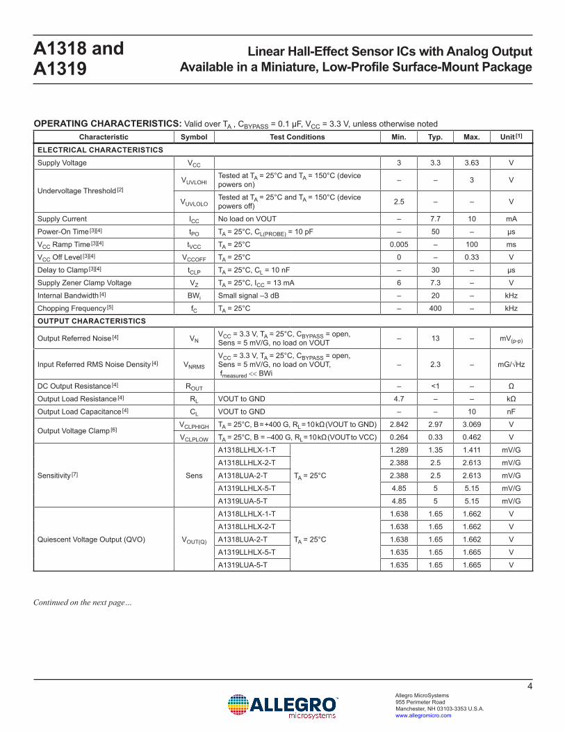
OPERATING CHARACTERISTICS: Valid over TA , CBYPASS = 0.1 µF, VCC = 3.3 V, unless otherwise notedCharacteristic Symbol Test Conditions Min. Typ. Max. Unit [1]
Continued on the next page…
ELECTRICAL CHARACTERISTICS Supply Voltage VCC 3 3.3 3.63 V
Undervoltage Threshold [2]VUVLOHI
Tested at TA = 25°C and TA = 150°C (device powers on) – – 3 V
VUVLOLOTested at TA = 25°C and TA = 150°C (device powers off) 2.5 – – V
Supply Current ICC No load on VOUT – 7.7 10 mA
Power-On Time [3][4] tPO TA = 25°C, CL(PROBE) = 10 pF – 50 – µs
VCC Ramp Time [3][4] tVCC TA = 25°C 0.005 – 100 ms
VCC Off Level [3][4] VCCOFF TA = 25°C 0 – 0.33 V
Delay to Clamp [3][4] tCLP TA = 25°C, CL = 10 nF – 30 – µs
Supply Zener Clamp Voltage VZ TA = 25°C, ICC = 13 mA 6 7.3 – V
Internal Bandwidth [4] BWi Small signal –3 dB – 20 – kHz
Chopping Frequency [5] fC TA = 25°C – 400 – kHz
OUTPUT CHARACTERISTICS
Output Referred Noise [4] VNVCC = 3.3 V, TA = 25°C, CBYPASS = open, Sens = 5 mV/G, no load on VOUT – 13 – mV(p-p)
Input Referred RMS Noise Density [4] VNRMS
VCC = 3.3 V, TA = 25°C, CBYPASS = open, Sens = 5 mV/G, no load on VOUT, fmeasured << BWi
– 2.3 – mG/√Hz
DC Output Resistance [4] ROUT – <1 – Ω
Output Load Resistance [4] RL VOUT to GND 4.7 – – kΩ
Output Load Capacitance [4] CL VOUT to GND – – 10 nF
Output Voltage Clamp [6]VCLPHIGH TA = 25°C, B = +400 G, RL = 10 kΩ (VOUT to GND) 2.842 2.97 3.069 V
VCLPLOW TA = 25°C, B = –400 G, RL = 10 kΩ (VOUT to VCC) 0.264 0.33 0.462 V
Sensitivity [7] Sens
A1318LLHLX-1-T
TA = 25°C
1.289 1.35 1.411 mV/G
A1318LLHLX-2-T 2.388 2.5 2.613 mV/G
A1318LUA-2-T 2.388 2.5 2.613 mV/G
A1319LLHLX-5-T 4.85 5 5.15 mV/G
A1319LUA-5-T 4.85 5 5.15 mV/G
Quiescent Voltage Output (QVO) VOUT(Q)
A1318LLHLX-1-T
TA = 25°C
1.638 1.65 1.662 V
A1318LLHLX-2-T 1.638 1.65 1.662 V
A1318LUA-2-T 1.638 1.65 1.662 V
A1319LLHLX-5-T 1.635 1.65 1.665 V
A1319LUA-5-T 1.635 1.65 1.665 V

Linear Hall-Effect Sensor ICs with Analog Output Available in a Miniature, Low-Profile Surface-Mount Package
A1318 and A1319
5Allegro MicroSystems 955 Perimeter Road Manchester, NH 03103-3353 U.S.A.www.allegromicro.com
OPERATING CHARACTERISTICS (continued): Valid over TA , CBYPASS = 0.1 µF, VCC = 3.3 V, unless otherwise notedCharacteristic Symbol Test Conditions Min. Typ. Max. Unit [1]
ELECTRICAL CHARACTERISTICS (continued)
Sensitivity Temperature Coefficient TCSens
A1318LLHLX-1-T
Programmed at TA = 150°C, calculated relative to Sens at 25°C
0.08 0.12 0.16 %/°C
A1318LLHLX-2-T 0.08 0.12 0.16 %/°C
A1318LUA-2-T 0.08 0.12 0.16 %/°C
A1319LLHLX-5-T 0.08 0.12 0.16 %/°C
A1319LUA-5-T 0.08 0.12 0.16 %/°C
ERROR COMPONENTS Linearity Sensitivity Error LinERR – ±1.5 – %
Symmetry Sensitivity Error SymERR – ±1.5 – %
Ratiometry Quiescent Voltage Output Error [8] RatVOUT(Q)
Across supply voltage range (relative to VCC = 5 V) – ±1.5 – %
Ratiometry Sensitivity Error [8] RatSensAcross supply voltage range (relative to VCC = 5 V) – ±1.5 – %
Ratiometry Clamp Error [9] RatVOUTCLPTA = 25°C, across supply voltage range (relative to VCC = 5 V) – ±1.5 – %
DRIFT CHARACTERISTICS
Typical Quiescent Voltage Output Drift Across Temperature Range ∆VOUT(Q)
A1318LLHLX-1-T
TA = 150°C
–15 – 5 mV
A1318LLHLX-2-T –18 – 8 mV
A1318LUA-2-T –13 0 13 mV
A1319LLHLX-5-T –20 – 20 mV
A1319LUA-5-T –15 0 15 mV
Sensitivity Drift Due to Package Hysteresis ∆SensPKG TA = 25°C, after temperature cycling – ±2 – %
[1] 1 G (gauss) = 0.1 mT (millitesla),[2] On power-up, the output of the device is held low until VCC exceeds VUVLOHI. After the device is powered, the output remains valid until VCC drops
below VUVLOLO , when the output is pulled low.[3] See the Characteristic Definitions section.[4] Determined by design and characterization, not evaluated at final test.[5] fC varies as much as approximately ±20% across the full operating ambient temperature range and process.[6] VCLPLOW and VCLPHIGH scale with VCC due to ratiometry.[7] Sensitivity drift through the life of the part, ΔSensLIFE , can have a typical error value ±3% in addition to package hysteresis effects.[8] Percent change from actual value at VCC = 3.3 V, for a given temperature.[9] Percent change from actual value at VCC = 3.3 V, TA = 25°C.

Linear Hall-Effect Sensor ICs with Analog Output Available in a Miniature, Low-Profile Surface-Mount Package
A1318 and A1319
6Allegro MicroSystems 955 Perimeter Road Manchester, NH 03103-3353 U.S.A.www.allegromicro.com
CHARACTERISTIC DEFINITIONS
Power-On Time. When the supply is ramped to its operating voltage, the device output requires a finite time to react to an input magnetic field. Power-On Time, tPO , is defined as the time it takes for the output voltage to begin responding to an applied magnetic field after the power supply has reached its minimum specified operating voltage, VCC(min), as shown in figure 1.
Delay to Clamp. A large magnetic input step may cause the clamp to overshoot its steady state value. The Delay to Clamp, tCLP , is defined as the time it takes for the output voltage to settle within 1% of its steady state value, after initially passing through its steady state voltage, as shown in figure 2.
Quiescent Voltage Output. In the quiescent state (no signifi-cant magnetic field: B = 0 G), the output, VOUT(Q), is at a con-stant ratio to the supply voltage, VCC, across the entire operating ranges of VCC and Operating Ambient Temperature, TA.
Quiescent Voltage Output Drift Across Temperature. Range Due to internal component tolerances and thermal considerations, the Quiescent Voltage Output, VOUT(Q), may drift due to temperature changes within the Operating Ambient Temperature, TA. For purposes of specification, the Quiescent Voltage Output Drift Across Temperature Range, ∆VOUT(Q) (mV), is defined as:
∆VOUT(Q) VOUT(Q)(TA) –VOUT(Q)(25°C)=
(1)
Sensitivity. The amount of the output voltage change is propor-tional to the magnitude and polarity of the magnetic field applied. This proportionality is specified as the magnetic sensitivity, Sens (mV/G), of the device and is defined as:
VOUT(B+) – VOUT(B–)
(B+) – (B–)Sens =
(2)
where B+ is the magnetic flux density in a positive field (south polarity) and B– is the magnetic flux density in a negative field (north polarity).
Sensitivity Temperature Coefficient. The device sensitiv-ity changes as temperature changes, with respect to its Sensitiv-ity Temperature Coefficient, TCSENS. TCSENS is programmed at 150°C, and calculated relative to the baseline sensitivity program-ming temperature of 25°C. TCSENS is defined as:
SensT2 – SensT1
SensT1 T2–T11
TCSens = × 100 (%/°C)
(3)
where T1 is the baseline Sens programming temperature of 25°C, and T2 is the TCSENS programming temperature of 150°C.
The ideal value of Sens across the full ambient temperature range, SensIDEAL(TA), is defined as:
SensT1 × [100 (%) + TCSENS (TA –T1)]SensIDEAL(TA) =
(4)
Sensitivity Drift Across Temperature Range. Second order sensitivity temperature coefficient effects cause the magnetic sensitivity, Sens, to drift from its ideal value across the operating ambient temperature range, TA. For purposes of specification,
V
+t
VCC
VCC(min)
VOUT90% VOUT
0
t1= time at which power supply reaches minimum specified operating voltage
t2= time at which output voltage settles within ±10% of its steady state value under an applied magnetic field
t1 t2tPO
VCC(typ)
time (µs)
Magnetic Input Signal
Mag
netic
Inpu
t Sig
nal
t1= time at which output voltage initially reaches steady state clamp voltage
t2= time at which output voltage settles to within 1% of steady state clamp voltage
VCLPHIGH
t1 t2
tCLP
VOUT
Dev
ice
Out
put,
V OU
T (V
)
Figure 1. Definition of Power On Time, tPO
Figure 2. Definition of Delay to Clamp, tCLP

Linear Hall-Effect Sensor ICs with Analog Output Available in a Miniature, Low-Profile Surface-Mount Package
A1318 and A1319
7Allegro MicroSystems 955 Perimeter Road Manchester, NH 03103-3353 U.S.A.www.allegromicro.com
the Sensitivity Drift Across Temperature Range, ∆SensTC, is defined as:
SensTA – SensIDEAL(TA)
SensIDEAL(TA)∆SensTC = × 100 (%)
(5)
Sensitivity Drift Due to Package Hysteresis. Package stress and relaxation can cause the device sensitivity at TA = 25°C to change during and after temperature cycling. This change in sensitivity follows a hysteresis curve. For purposes of specifica-tion, the Sensitivity Drift Due to Package Hysteresis, ∆SensPKG, is defined as:
Sens(25°C)(2) – Sens(25°C)(1)
Sens(25°C)(1)∆SensPKG = × 100 (%)
(6)
where Sens(25°C)(1) is the programmed value of sensitivity at TA = 25°C, and Sens(25°C)(2) is the value of sensitivity at TA = 25°C after temperature cycling TA up to 150°C, down to –40°C, and back to up 25°C.
Linearity Sensitivity Error. The A1318 and A1319 are designed to provide linear output in response to a ramping applied magnetic field. Consider two magnetic fields, B1 and B2. Ideally, the sensitivity of a device is the same for both fields, for a given supply voltage and temperature. Linearity error is present when there is a difference between the sensitivities measured at B1 and B2.
Linearity Sensitivity Error, LINERR , is calculated separately for positive (LinERR+) and negative (LinERR– ) applied magnetic fields. LINERR (%) is measured and defined as:
Sens(B+)(2)
Sens(B+)(1)
Sens(B–)(2)
Sens(B–)(1)
1–LinERR+ = × 100 (%)
× 100 (%)
1–LinERR– =
(7)
where:
|VOUT(Bx) – VOUT(Q)|
BxSensBx =
(8)
and Bx are positive and negative magnetic fields, with respect to the quiescent voltage output, such that
|B(+)(2)| > |B(+)(1)| and |B(–)(2)| > |B(–)(1)|
The effective linearity error is:
max(|LinERR+| , |LinERR– |)LinERR =
(9)
The output voltage clamps, VCLPHIGH and VCLPLOW , limit the operating magnetic range of the applied field in which the device provides a linear output. The maximum positive and negative applied magnetic fields in the operating range can be calculated:
VCLPHIGH – VOUT(Q)
SensBMAX(+) =
VOUT(Q) – VCLPLOW
SensBMAX(–) =
(10)
Symmetry Sensitivity Error. The magnetic sensitivity of the device is constant for any two applied magnetic fields of equal magnitude and opposite polarities. Symmetry error, SymERR (%), is measured and defined as:
Sens(B+)
Sens(B–)1–SymERR = × 100 (%)
(11)
where SensBx is as defined in equation 10, and B+ and B– are positive and negative magnetic fields such that |B+| = |B–|.
Ratiometry Error. The A1318 and A1319 provide ratiometric output. This means that the Quiescent Voltage Output, VOUT(Q) , magnetic sensitivity, Sens, and clamp voltages, VCLPHIGH and VCLPLOW , are proportional to the supply voltage, VCC. In other words, when the supply voltage increases or decreases by a certain percentage, each characteristic also increases or decreases by the same percentage. Error is the difference between the measured change in the supply voltage relative to 3.3 V, and the measured change in each characteristic.
The ratiometric error in quiescent voltage output, RatVOUT(Q) (%), for a given supply voltage, VCC, is defined as:
VOUT(Q)(VCC) / VOUT(Q)(3.3V)
VCC / 3.3 (V)1–RatVOUT(Q) = × 100 (%)
(12)
The ratiometric error in magnetic sensitivity, RatSens (%), for a given supply voltage, VCC, is defined as:
Sens(VCC) / Sens(3.3V)
VCC / 3.3 (V)1–RatSens = × 100 (%)
(13)
The ratiometric error in the clamp voltages, RatVOUTCLP (%), for a given supply voltage, VCC, is defined as:
VCLP(VCC) / VCLP(3.3V)
VCC / 3.3 (V)1–RatVOUTCLP = × 100 (%)
(14)
where VCLP is either VCLPHIGH or VCLPLOW .

Linear Hall-Effect Sensor ICs with Analog Output Available in a Miniature, Low-Profile Surface-Mount Package
A1318 and A1319
8Allegro MicroSystems 955 Perimeter Road Manchester, NH 03103-3353 U.S.A.www.allegromicro.com
Undervoltage Lockout. The A1318 and A1319 provide an undervoltage lockout feature which ensures that the device out-puts a VOUT signal only when VCC is above certain thresholds . The undervoltage lockout feature provides a hysteresis of opera-tion to eliminate indeterminate output states.
The output of the A1318 and A1319 is held low (GND) until VCC exceeds VUVLOHI . After VCC exceeds VUVLOHI , the device VOUT output is enabled, providing a ratiometric output volt-age that is proportional to the input magnetic signal and VCC . If VCC should drop back down below VUVLOLO after the device is powered up, the output would be pulled low (see figure 3) until VUVLOHI is reached again and VOUT would be reenabled.
VCC Ramp Time. The time taken for VCC to ramp from 0 V to VCC(typ), 3.3 V (see figure 4).
VCC Off Level. For applications in which the VCC pin of the A1318 or A1319 is being power-cycled (for example using a multiplexer to toggle the part on and off), the specification of VCC Off Level, VCCOFF , determines how high a VCC off voltage can be tolerated while still ensuring proper operation and startup of the device (see figure 4).
Figure 3. Definition of Undervoltage Lockout
VOUT
VCC
VUVLOHI
VUVLOLO
time
time
VCC(typ)
VCCOFF
0
tVCCS
uppl
y Vo
ltage
, VC
C (V
)
Figure 4. Definition of VCC Ramp Time, tVCC

Linear Hall-Effect Sensor ICs with Analog Output Available in a Miniature, Low-Profile Surface-Mount Package
A1318 and A1319
9Allegro MicroSystems 955 Perimeter Road Manchester, NH 03103-3353 U.S.A.www.allegromicro.com
A1318A1319
VOUT
GND0.13.3 V µFRL
VCC
4.7 nF
APPLICATION INFORMATION
Figure 5. Typical Application Circuit
Figure 6. Chopper Stabilization Technique
Chopper Stabilization TechniqueWhen using Hall-effect technology, a limiting factor for switchpoint accuracy is the small signal voltage developed across the Hall element. This voltage is disproportionally small relative to the offset that can be produced at the output of the Hall sensor IC. This makes it difficult to process the signal while maintain-ing an accurate, reliable output over the specified operating temperature and voltage ranges. Chopper stabilization is a unique approach used to minimize Hall offset on the chip. Allegro employs a technique to remove key sources of the output drift induced by thermal and mechanical stresses. This offset reduction technique is based on a signal modulation-demodulation process. The undesired offset signal is separated from the magnetic field-induced signal in the frequency domain, through modulation. The subsequent demodulation acts as a modulation process for the offset, causing the magnetic field-induced signal to recover its original spectrum at base band, while the DC offset becomes a high-frequency signal. The magnetic-sourced signal then can pass
through a low-pass filter, while the modulated DC offset is sup-pressed. In addition to the removal of the thermal and mechanical stress related offset, this novel technique also reduces the amount of thermal noise in the Hall sensor IC while completely removing the modulated residue resulting from the chopper operation. The chopper stabilization technique uses a high frequency sampling clock. For demodulation process, a sample and hold technique is used. This high-frequency operation allows a greater sampling rate, which results in higher accuracy and faster signal-processing capability. This approach desensitizes the chip to the effects of thermal and mechanical stresses, and produces devices that have extremely stable quiescent Hall output voltages and precise recoverability after temperature cycling. This technique is made possible through the use of a BiCMOS process, which allows the use of low-offset, low-noise amplifiers in combination with high-density logic integration and sample-and-hold circuits.
Amp
Regulator
Clock/Logic
Hall Element
TunedFilter
Anti-aliasingLP Filter
Linear Hall-Effect Sensor ICs with Analog Output Available in a Miniature, Low-Profile Surface-Mount Package
A1318 and A1319
10Allegro MicroSystems 955 Perimeter Road Manchester, NH 03103-3353 U.S.A.www.allegromicro.com
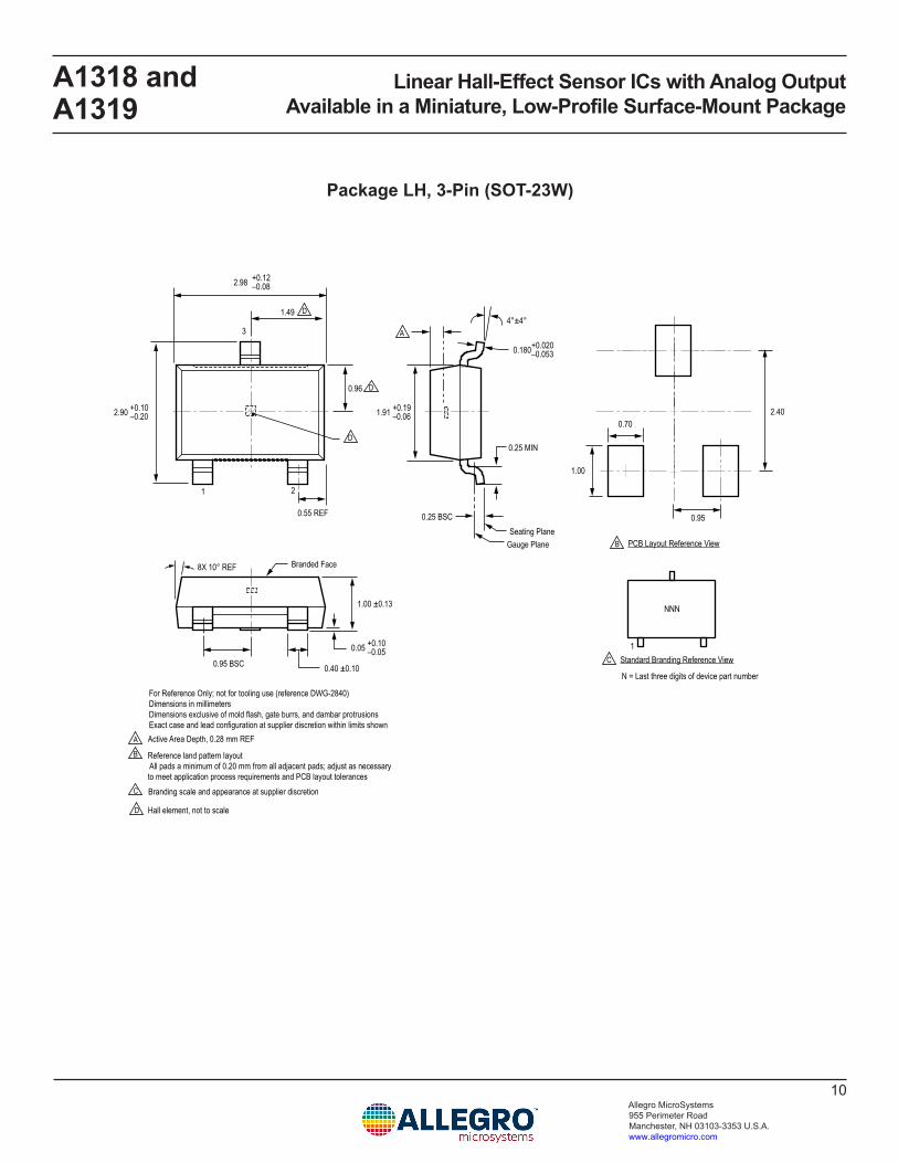
Package LH, 3-Pin (SOT-23W)
0.55 REF
Gauge PlaneSeating Plane
0.25 BSC
0.95 BSC
0.95
1.00
0.70 2.40
21
A Active Area Depth, 0.28 mm REFB
C
C
B
Reference land pattern layout All pads a minimum of 0.20 mm from all adjacent pads; adjust as necessary to meet application process requirements and PCB layout tolerancesBranding scale and appearance at supplier discretion
A
PCB Layout Reference View
Standard Branding Reference View1
Branded Face
N = Last three digits of device part number
NNN
2.90 +0.10–0.20
4°±4°
8X 10° REF
0.180+0.020–0.053
0.05 +0.10–0.05
0.25 MIN
1.91 +0.19–0.06
2.98 +0.12–0.08
1.00 ±0.13
0.40 ±0.10
For Reference Only; not for tooling use (reference DWG-2840)Dimensions in millimetersDimensions exclusive of mold flash, gate burrs, and dambar protrusions Exact case and lead configuration at supplier discretion within limits shown
D Hall element, not to scale
D
D
D1.49
0.96
3

Linear Hall-Effect Sensor ICs with Analog Output Available in a Miniature, Low-Profile Surface-Mount Package
A1318 and A1319
11Allegro MicroSystems 955 Perimeter Road Manchester, NH 03103-3353 U.S.A.www.allegromicro.com
Package UA, 3-Pin SIP
2 31
1.27 NOM
1.02 MAX
45°
45°
C
1.52 ±0.05
B
Gate and tie bar burr areaA
B
C
Dambar removal protrusion (6X)
A
D
E
E
E
1.44
2.04
E
Active Area Depth, 0.50 mm REF
Branding scale and appearance at supplier discretionHall element (not to scale)
For Reference Only; not for tooling use (reference DWG-9065)Dimensions in millimetersDimensions exclusive of mold flash, gate burrs, and dambar protrusions Exact case and lead configuration at supplier discretion within limits shown
Mold EjectorPin Indent
D Standard Branding Reference View
= Supplier emblem N = Last three digits of device part number
NNN
1
0.41 +0.03–0.06
0.43 +0.05–0.07
14.99 ±0.25
4.09 +0.08–0.05
3.02 +0.08–0.05
0.79 REF
10°
Branded Face

Linear Hall-Effect Sensor ICs with Analog Output Available in a Miniature, Low-Profile Surface-Mount Package
A1318 and A1319
12Allegro MicroSystems 955 Perimeter Road Manchester, NH 03103-3353 U.S.A.www.allegromicro.com
For the latest version of this document, visit our website:www.allegromicro.com
Revision HistoryNumber Date Description
1 June 27, 2014 Updated product offerings, VCLPHIGH
2 April 8, 2016 Updated Selection Guide table
3 January 3, 2018 Updated Selection Guide table
4 January 15, 2019 Minor editorial updates
5 January 31, 2020 Minor editorial updates
6 October 22, 2020 Updated product status to NND
Copyright 2020, Allegro MicroSystems.Allegro MicroSystems reserves the right to make, from time to time, such departures from the detail specifications as may be required to permit
improvements in the performance, reliability, or manufacturability of its products. Before placing an order, the user is cautioned to verify that the information being relied upon is current.
Allegro’s products are not to be used in any devices or systems, including but not limited to life support devices or systems, in which a failure of Allegro’s product can reasonably be expected to cause bodily harm.
The information included herein is believed to be accurate and reliable. However, Allegro MicroSystems assumes no responsibility for its use; nor for any infringement of patents or other rights of third parties which may result from its use.
Copies of this document are considered uncontrolled documents.