lm10 operational amplifier and voltage reference
TRANSCRIPT
LM10Operational Amplifier and Voltage ReferenceGeneral DescriptionThe LM10 series are monolithic linear ICs consisting of aprecision reference, an adjustable reference buffer and anindependent, high quality op amp.
The unit can operate from a total supply voltage as low as1.1V or as high as 40V, drawing only 270µA. A complemen-tary output stage swings within 15 mV of the supply termi-nals or will deliver ±20 mA output current with ±0.4V satu-ration. Reference output can be as low as 200 mV.
The circuit is recommended for portable equipment and iscompletely specified for operation from a single power cell.In contrast, high output-drive capability, both voltage andcurrent, along with thermal overload protection, suggest it indemanding general-purpose applications.
The device is capable of operating in a floating mode, inde-pendent of fixed supplies. It can function as a remote com-parator, signal conditioner, SCR controller or transmitter for
analog signals, delivering the processed signal on the sameline used to supply power. It is also suited for operation in awide range of voltage- and current-regulator applications,from low voltages to several hundred volts, providing greaterprecision than existing ICs.
This series is available in the three standard temperatureranges, with the commercial part having relaxed limits. Inaddition, a low-voltage specification (suffix “L”) is available inthe limited temperature ranges at a cost savings.
Featuresn input offset voltage: 2.0 mV (max)n input offset current: 0.7 nA (max)n input bias current: 20 nA (max)n reference regulation: 0.1% (max)n offset voltage drift: 2µV/˚Cn reference drift: 0.002%/˚C
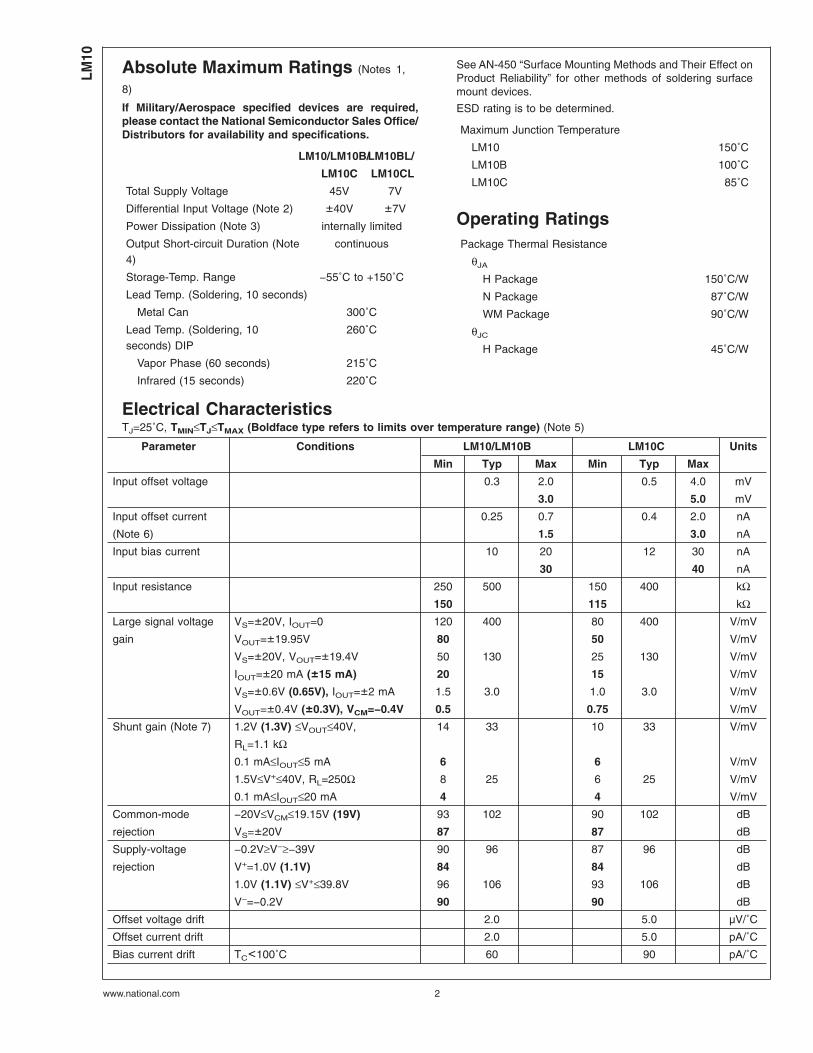
Connection and Functional Diagrams
Metal Can Package (H)
00565201
Order Number LM10BH, LM10CH,LM10CLH or LM10H/883
available per SMA# 5962-8760401See NS Package Number H08A
Small Outline Package (WM)
00565217
Order Number LM10CWM or LM10CWMXSee NS Package Number M14B
Dual-In-Line Package (N)
00565215
Order Number LM10CN or LM10CLNSee NS Package Number N08E
00565216
August 2000LM
10O
perationalAm
plifierand
VoltageR
eference
© 2004 National Semiconductor Corporation DS005652 www.national.com
Absolute Maximum Ratings (Notes 1,
8)
If Military/Aerospace specified devices are required,please contact the National Semiconductor Sales Office/Distributors for availability and specifications.
LM10/LM10B/LM10BL/
LM10C LM10CL
Total Supply Voltage 45V 7V
Differential Input Voltage (Note 2) ±40V ±7V
Power Dissipation (Note 3) internally limited
Output Short-circuit Duration (Note4)
continuous
Storage-Temp. Range −55˚C to +150˚C
Lead Temp. (Soldering, 10 seconds)
Metal Can 300˚C
Lead Temp. (Soldering, 10seconds) DIP
260˚C
Vapor Phase (60 seconds) 215˚C
Infrared (15 seconds) 220˚C
See AN-450 “Surface Mounting Methods and Their Effect onProduct Reliability” for other methods of soldering surfacemount devices.
ESD rating is to be determined.
Maximum Junction Temperature
LM10 150˚C
LM10B 100˚C
LM10C 85˚C
Operating RatingsPackage Thermal Resistance
θJA
H Package 150˚C/W
N Package 87˚C/W
WM Package 90˚C/W
θJC
H Package 45˚C/W
Electrical CharacteristicsTJ=25˚C, TMIN≤TJ≤TMAX (Boldface type refers to limits over temperature range) (Note 5)
Parameter Conditions LM10/LM10B LM10C Units
Min Typ Max Min Typ Max
Input offset voltage 0.3 2.0 0.5 4.0 mV
3.0 5.0 mV
Input offset current 0.25 0.7 0.4 2.0 nA
(Note 6) 1.5 3.0 nA
Input bias current 10 20 12 30 nA
30 40 nA
Input resistance 250 500 150 400 kΩ150 115 kΩ
Large signal voltage VS=±20V, IOUT=0 120 400 80 400 V/mV
gain VOUT=±19.95V 80 50 V/mV
VS=±20V, VOUT=±19.4V 50 130 25 130 V/mV
IOUT=±20 mA (±15 mA) 20 15 V/mV
VS=±0.6V (0.65V), IOUT=±2 mA 1.5 3.0 1.0 3.0 V/mV
VOUT=±0.4V (±0.3V), VCM=−0.4V 0.5 0.75 V/mV
Shunt gain (Note 7) 1.2V (1.3V) ≤VOUT≤40V, 14 33 10 33 V/mV
RL=1.1 kΩ0.1 mA≤IOUT≤5 mA 6 6 V/mV
1.5V≤V+≤40V, RL=250Ω 8 25 6 25 V/mV
0.1 mA≤IOUT≤20 mA 4 4 V/mV
Common-mode −20V≤VCM≤19.15V (19V) 93 102 90 102 dB
rejection VS=±20V 87 87 dB
Supply-voltage −0.2V≥V−≥−39V 90 96 87 96 dB
rejection V+=1.0V (1.1V) 84 84 dB
1.0V (1.1V) ≤V+≤39.8V 96 106 93 106 dB
V−=−0.2V 90 90 dB
Offset voltage drift 2.0 5.0 µV/˚C
Offset current drift 2.0 5.0 pA/˚C
Bias current drift TC<100˚C 60 90 pA/˚C
LM10
www.national.com 2
Electrical Characteristics (Continued)TJ=25˚C, TMIN≤TJ≤TMAX (Boldface type refers to limits over temperature range) (Note 5)
Parameter Conditions LM10/LM10B LM10C Units
Min Typ Max Min Typ Max
Line regulation 1.2V (1.3V) ≤VS≤40V 0.001 0.003 0.001 0.008 %/V
0≤IREF≤1.0 mA, VREF=200 mV 0.006 0.01 %/V
Load regulation 0≤IREF≤1.0 mA 0.01 0.1 0.01 0.15 %
V+−VREF≥1.0V (1.1V) 0.15 0.2 %
Amplifier gain 0.2V≤VREF≤35V 50 75 25 70 V/mV
23 15 V/mV
Feedback sense 195 200 205 190 200 210 mV
voltage 194 206 189 211 mV
Feedback current 20 50 22 75 nA
65 90 nA
Reference drift 0.002 0.003 %/˚C
Supply current 270 400 300 500 µA
500 570 µA
Supply currentchange
1.2V (1.3V) ≤VS≤40V 15 75 15 75 µA
Electrical CharacteristicsTJ=25˚C, TMIN≤TJ≤TMAX (Boldface type refers to limits over temperature range) (Note 5)
Parameter Conditions LM10BL LM10CL Units
Min Typ Max Min Typ Max
Input offset voltage 0.3 2.0 0.5 4.0 mV
3.0 5.0 mV
Input offset current 0.1 0.7 0.2 2.0 nA
(Note 6) 1.5 3.0 nA
Input bias current 10 20 12 30 nA
30 40 nA
Input resistance 250 500 150 400 kΩ150 115 kΩ
Large signal voltage VS=±3.25V, IOUT=0 60 300 40 300 V/mV
gain VOUT=±3.2V 40 25 V/mV
VS=±3.25V, IOUT=10 mA 10 25 5 25 V/mV
VOUT=±2.75 V 4 3 V/mV
VS=±0.6V (0.65V), IOUT=±2 mA 1.5 3.0 1.0 3.0 V/mV
VOUT=±0.4V (±0.3V), VCM=−0.4V 0.5 0.75 V/mV
Shunt gain (Note 7) 1.5V≤V+≤6.5V, RL=500Ω 8 30 6 30 V/mV
0.1 mA≤IOUT≤10 mA 4 4 V/mV
Common-mode −3.25V≤VCM≤2.4V (2.25V) 89 102 80 102 dB
rejection VS=±3.25V 83 74 dB
Supply-voltage −0.2V≥V−≥−5.4V 86 96 80 96 dB
rejection V+=1.0V (1.2V) 80 74 dB
1.0V (1.1V) ≤V+≤6.3V 94 106 80 106 dB
V−=0.2V 88 74 dB
Offset voltage drift 2.0 5.0 µV/˚C
Offset current drift 2.0 5.0 pA/˚C
Bias current drift 60 90 pA/˚C
Line regulation 1.2V (1.3V) ≤VS≤6.5V 0.001 0.01 0.001 0.02 %/V
0≤IREF≤0.5 mA, VREF=200 mV 0.02 0.03 %/V
LM10
www.national.com3
Electrical Characteristics (Continued)TJ=25˚C, TMIN≤TJ≤TMAX (Boldface type refers to limits over temperature range) (Note 5)
Parameter Conditions LM10BL LM10CL Units
Min Typ Max Min Typ Max
Load regulation 0≤IREF≤0.5 mA 0.01 0.1 0.01 0.15 %
V+−VREF≥1.0V (1.1V) 0.15 0.2 %
Amplifier gain 0.2V≤VREF≤5.5V 30 70 20 70 V/mV
20 15 V/mV
Feedback sense voltage 195 200 205 190 200 210 mV
194 206 189 211 mV
Feedback current 20 50 22 75 nA
65 90 nA
Reference drift 0.002 0.003 %/˚C
Supply current 260 400 280 500 µA
500 570 µA
Note 1: Absolute Maximum Ratings indicate limits beyond which damage to the device may occur. Operating Ratings indicate conditions for which the device isfunctional, but do not guarantee specific performance limits.
Note 2: The Input voltage can exceed the supply voltages provided that the voltage from the input to any other terminal does not exceed the maximum differentialinput voltage and excess dissipation is accounted for when VIN<V−.
Note 3: The maximum, operating-junction temperature is 150˚C for the LM10, 100˚C for the LM10B(L) and 85˚C for the LM10C(L). At elevated temperatures,devices must be derated based on package thermal resistance.
Note 4: Internal thermal limiting prevents excessive heating that could result in sudden failure, but the IC can be subjected to accelerated stress with a shortedoutput and worst-case conditions.
Note 5: These specifications apply for V−≤VCM≤V+−0.85V (1.0V), 1.2V (1.3V) <VS≤VMAX, VREF=0.2V and 0≤IREF≤1.0 mA, unless otherwise specified: VMAX=40Vfor the standard part and 6.5V for the low voltage part. Normal typeface indicates 25˚C limits. Boldface type indicates limits and altered test conditions forfull-temperature-range operation; this is −55˚C to 125˚C for the LM10, −25˚C to 85˚C for the LM10B(L) and 0˚C to 70˚C for the LM10C(L). The specifications donot include the effects of thermal gradients (τ1.20 ms), die heating (τ2.0.2s) or package heating. Gradient effects are small and tend to offset the electrical error(see curves).
Note 6: For TJ>90˚C, IOS may exceed 1.5 nA for VCM=V−. With TJ=125˚C and V−≤VCM≤V−+0.1V, IOS≤5 nA.
Note 7: This defines operation in floating applications such as the bootstrapped regulator or two-wire transmitter. Output is connected to the V+ terminal of the ICand input common mode is referred to V− (see typical applications). Effect of larger output-voltage swings with higher load resistance can be accounted for by addingthe positive-supply rejection error.
Note 8: Refer to RETS10X for LM10H military specifications.
Definition of TermsInput offset voltage: That voltage which must be applied between the input terminals to bias the unloaded output in the linearregion.
Input offset current: The difference in the currents at the input terminals when the unloaded output is in the linear region.
Input bias current: The absolute value of the average of the two input currents.
Input resistance: The ratio of the change in input voltage to the change in input current on either input with the other grounded.
Large signal voltage gain: The ratio of the specified output voltage swing to the change in differential input voltage required toproduce it.
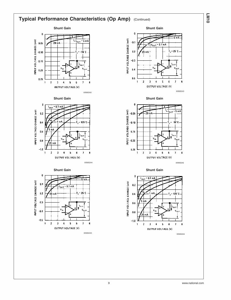
Shunt gain: The ratio of the specified output voltage swing to the change in differential input voltage required to produce it withthe output tied to the V+ terminal of the IC. The load and power source are connected between the V+ and V− terminals, and inputcommon-mode is referred to the V− terminal.
Common-mode rejection: The ratio of the input voltage range to the change in offset voltage between the extremes.
Supply-voltage rejection: The ratio of the specified supply-voltage change to the change in offset voltage between theextremes.
Line regulation: The average change in reference output voltage over the specified supply voltage range.
Load regulation: The change in reference output voltage from no load to that load specified.
Feedback sense voltage: The voltage, referred to V−, on the reference feedback terminal while operating in regulation.
Reference amplifier gain: The ratio of the specified reference output change to the change in feedback sense voltage requiredto produce it.
Feedback current: The absolute value of the current at the feedback terminal when operating in regulation.
Supply current: The current required from the power source to operate the amplifier and reference with their outputs unloadedand operating in the linear range.
LM10
www.national.com 4
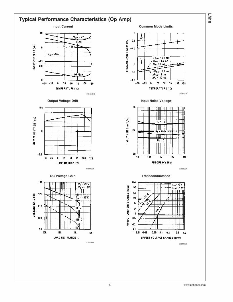
Typical Performance Characteristics (Op Amp)Input Current Common Mode Limits
00565218 00565219
Output Voltage Drift Input Noise Voltage
00565220 00565221
DC Voltage Gain Transconductance
0056522200565223
LM10
www.national.com5
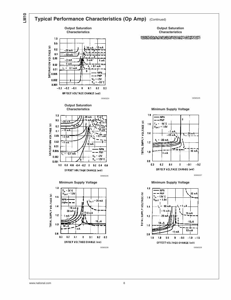
Typical Performance Characteristics (Op Amp) (Continued)
Output SaturationCharacteristics
Output SaturationCharacteristics
00565224 00565225
Output SaturationCharacteristics Minimum Supply Voltage
00565226 00565227
Minimum Supply Voltage Minimum Supply Voltage
00565228 00565229
LM10
www.national.com 6
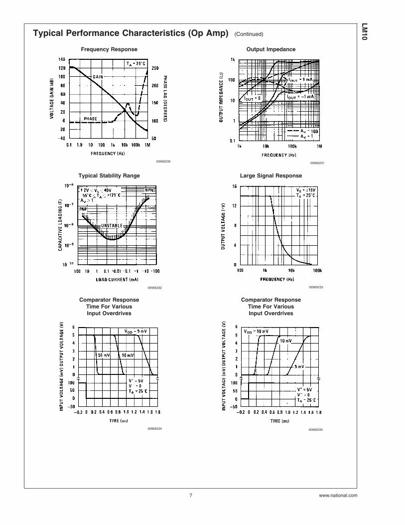
Typical Performance Characteristics (Op Amp) (Continued)
Frequency Response Output Impedance
00565230 00565231
Typical Stability Range Large Signal Response
00565232 00565233
Comparator ResponseTime For VariousInput Overdrives
Comparator ResponseTime For VariousInput Overdrives
00565234 00565235
LM10
www.national.com7
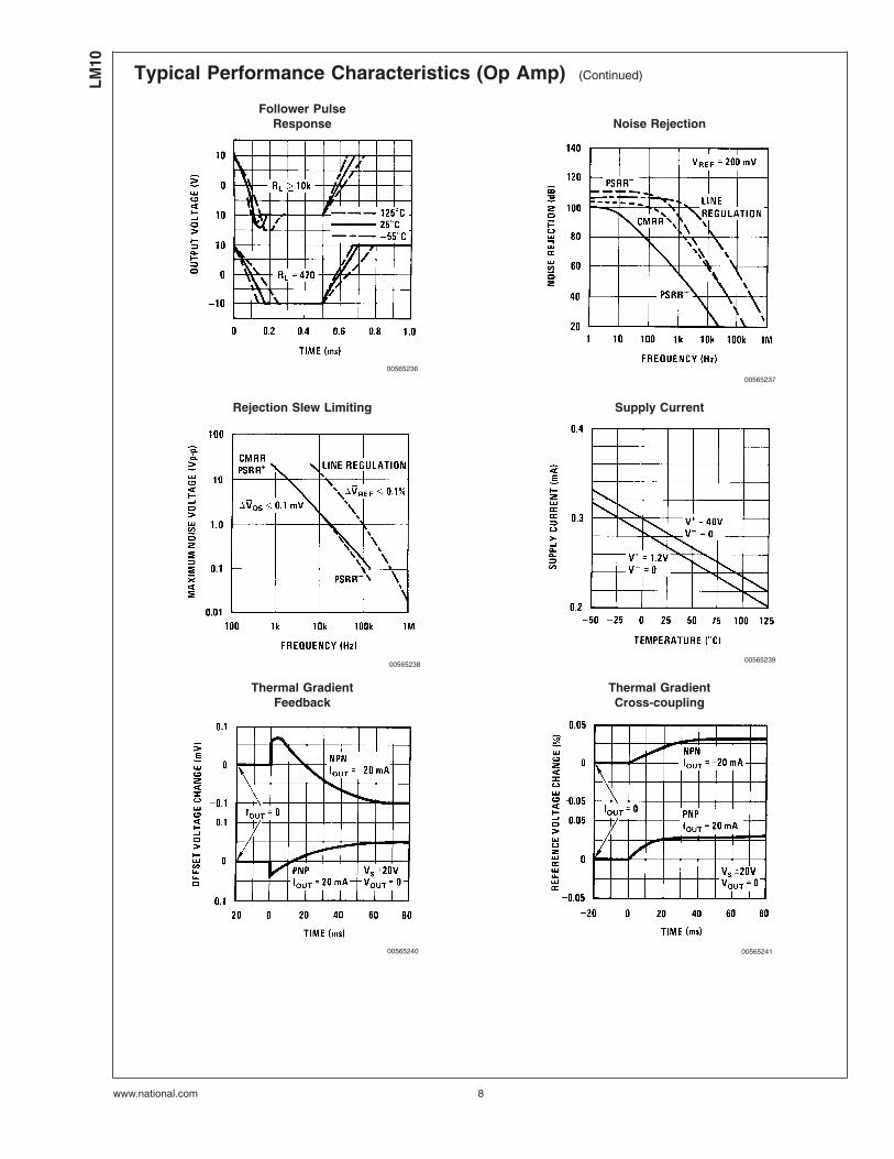
Typical Performance Characteristics (Op Amp) (Continued)
Follower PulseResponse Noise Rejection
00565236
00565237
Rejection Slew Limiting Supply Current
0056523800565239
Thermal GradientFeedback
Thermal GradientCross-coupling
00565240 00565241
LM10
www.national.com 8
Typical Performance Characteristics (Op Amp) (Continued)
Shunt Gain Shunt Gain
0056524200565243
Shunt Gain Shunt Gain
00565244 00565242
Shunt Gain Shunt Gain
00565243 00565244
LM10
www.national.com9
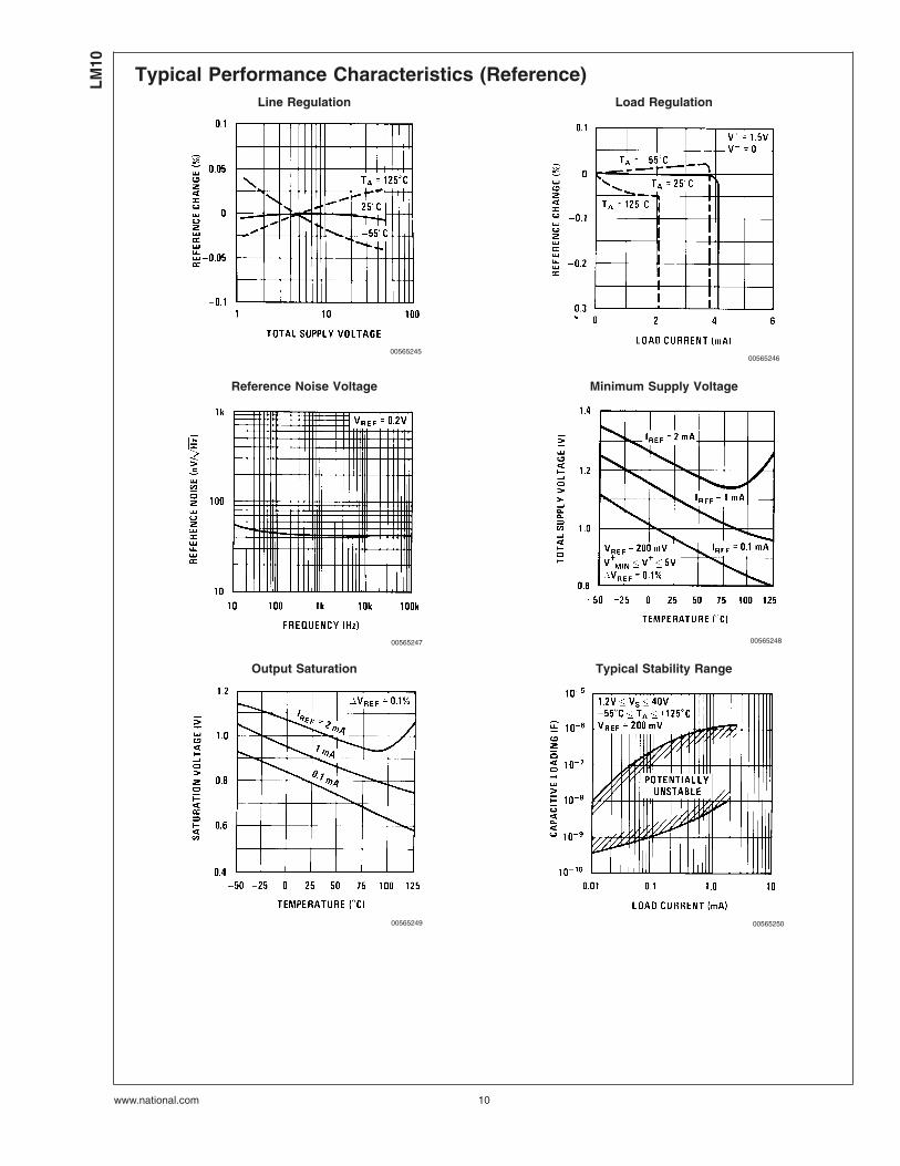
Typical Performance Characteristics (Reference)Line Regulation Load Regulation
0056524500565246
Reference Noise Voltage Minimum Supply Voltage
00565247 00565248
Output Saturation Typical Stability Range
00565249 00565250
LM10
www.national.com 10
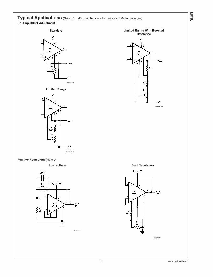
Typical Applications (Note 10) (Pin numbers are for devices in 8-pin packages)
Op Amp Offset Adjustment
Standard
00565251
Limited Range
00565252
Limited Range With BoostedReference
00565253
Positive Regulators (Note 9)
Low Voltage Best Regulation
00565254
00565255
LM10
www.national.com11
Typical Applications (Note 10) (Pin numbers are for devices in 8-pin packages) (Continued)
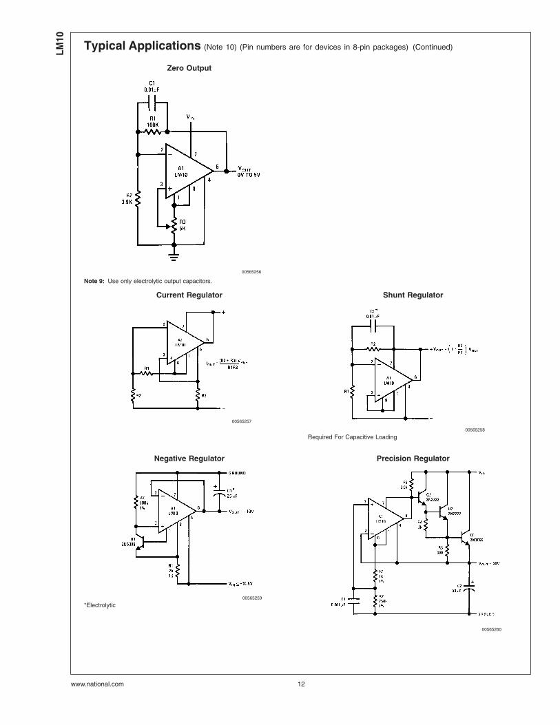
Zero Output
00565256
Note 9: Use only electrolytic output capacitors.
Current Regulator Shunt Regulator
00565257
00565258
Required For Capacitive Loading
Negative Regulator Precision Regulator
00565259
*Electrolytic
00565260
LM10
www.national.com 12
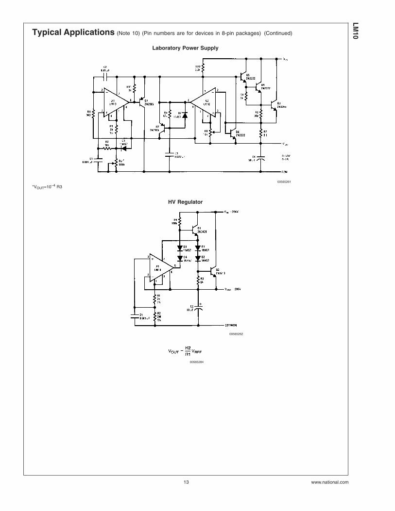
Typical Applications (Note 10) (Pin numbers are for devices in 8-pin packages) (Continued)
Laboratory Power Supply
00565261
*VOUT=10−4 R3
HV Regulator
00565262
00565284
LM10
www.national.com13
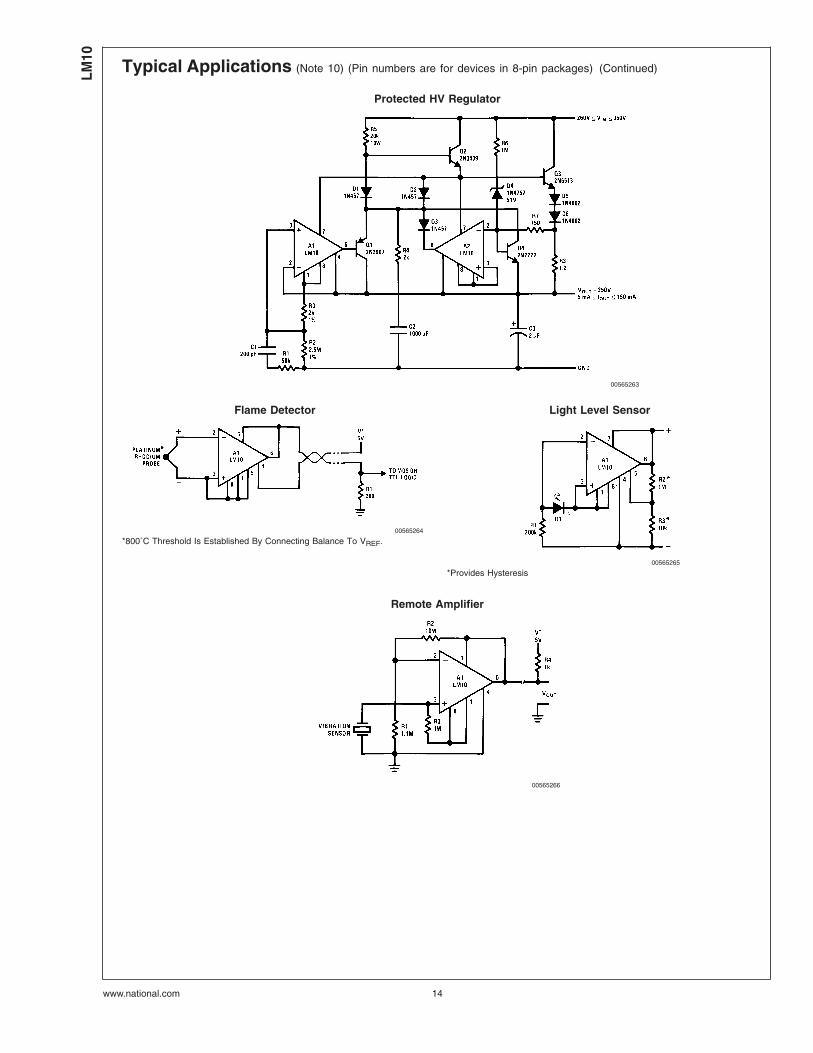
Typical Applications (Note 10) (Pin numbers are for devices in 8-pin packages) (Continued)
Protected HV Regulator
00565263
Flame Detector Light Level Sensor
00565264
*800˚C Threshold Is Established By Connecting Balance To VREF.
00565265
*Provides Hysteresis
Remote Amplifier
00565266
LM10
www.national.com 14
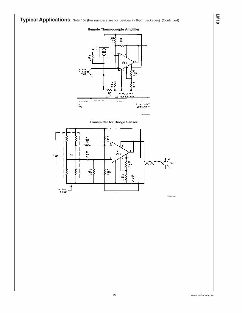
Typical Applications (Note 10) (Pin numbers are for devices in 8-pin packages) (Continued)
Remote Thermocouple Amplifier
00565267
Transmitter for Bridge Sensor
00565268
LM10
www.national.com15
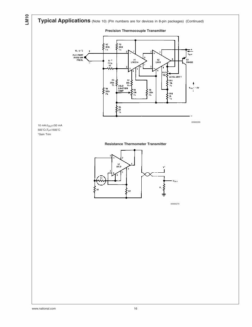
Typical Applications (Note 10) (Pin numbers are for devices in 8-pin packages) (Continued)
Precision Thermocouple Transmitter
00565269
10 mA≤IOUT≤50 mA
500˚C≤TP≤1500˚C
*Gain Trim
Resistance Thermometer Transmitter
00565270
LM10
www.national.com 16
Typical Applications (Note 10) (Pin numbers are for devices in 8-pin packages) (Continued)
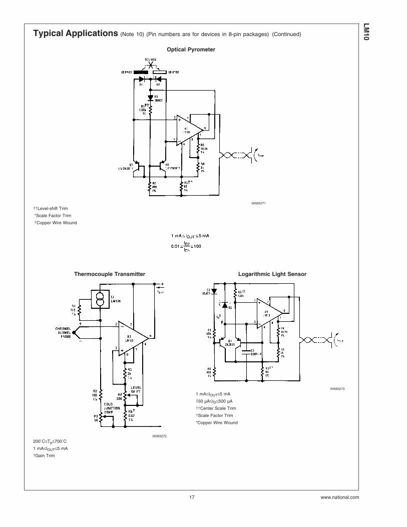
Optical Pyrometer
00565271
††Level-shift Trim
*Scale Factor Trim
†Copper Wire Wound
Thermocouple Transmitter Logarithmic Light Sensor
00565272
200˚C≤Tp≤700˚C
1 mA≤IOUT≤5 mA
†Gain Trim
00565273
1 mA≤IOUT≤5 mA
‡50 µA≤ID≤500 µA
††Center Scale Trim
†Scale Factor Trim
*Copper Wire Wound
LM10
www.national.com17
Typical Applications (Note 10) (Pin numbers are for devices in 8-pin packages) (Continued)
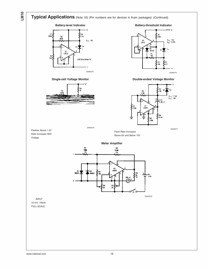
Battery-level Indicator Battery-threshold Indicator
0056527400565275
Single-cell Voltage Monitor Double-ended Voltage Monitor
00565276
Flashes Above 1.2V
Rate Increases With
Voltage
00565277
Flash Rate Increases
Above 6V and Below 15V
Meter Amplifier
00565278
INPUT
10 mV, 100nA
FULL-SCALE
LM10
www.national.com 18
Typical Applications (Note 10) (Pin numbers are for devices in 8-pin packages) (Continued)
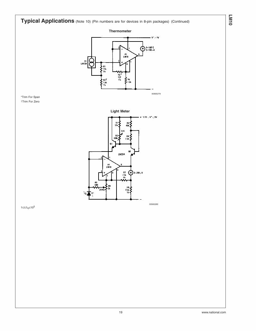
Thermometer
00565279
*Trim For Span
†Trim For Zero
Light Meter
00565280
1≤λ/λ0≤105
LM10
www.national.com19
Typical Applications (Note 10) (Pin numbers are for devices in 8-pin packages) (Continued)
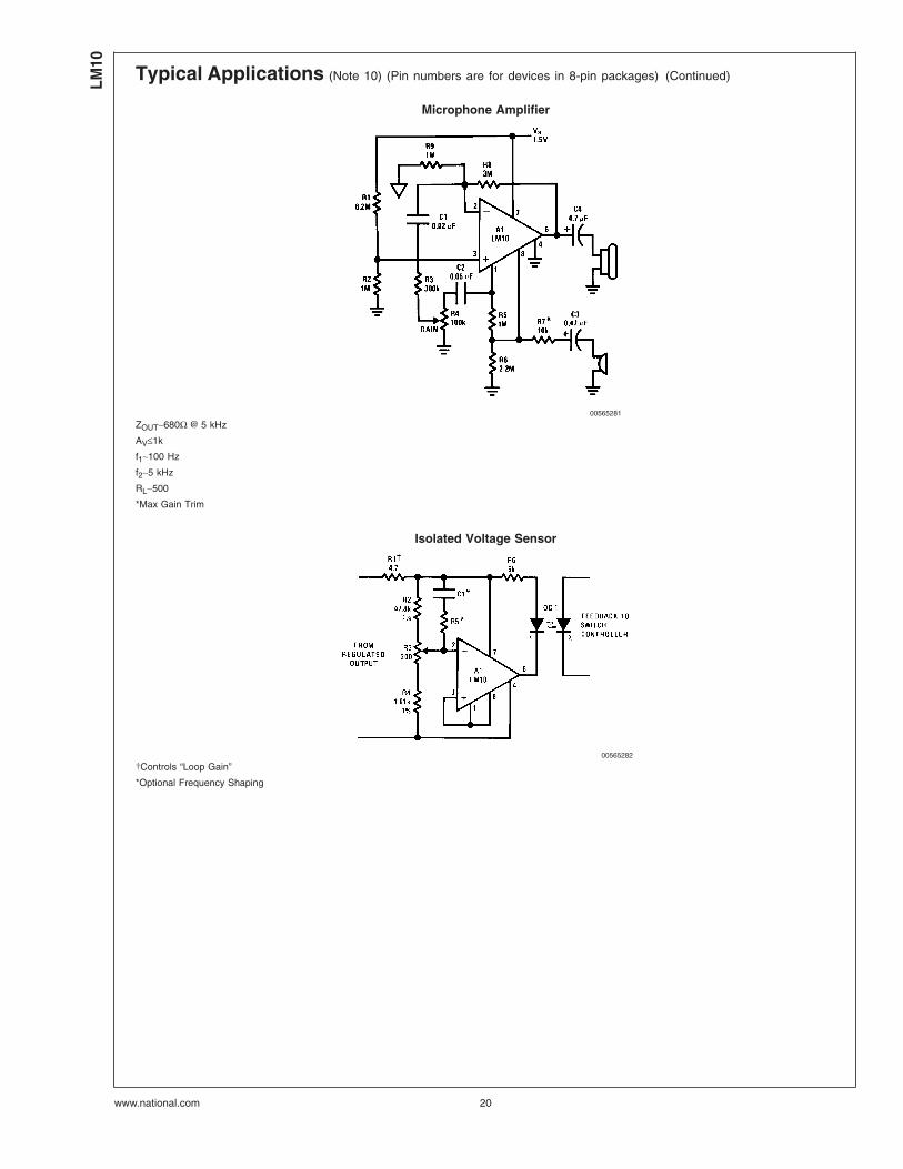
Microphone Amplifier
00565281
ZOUT∼680Ω @ 5 kHz
AV≤1k
f1∼100 Hz
f2∼5 kHz
RL∼500
*Max Gain Trim
Isolated Voltage Sensor
00565282
†Controls “Loop Gain”
*Optional Frequency Shaping
LM10
www.national.com 20
Typical Applications (Note 10) (Pin numbers are for devices in 8-pin packages) (Continued)
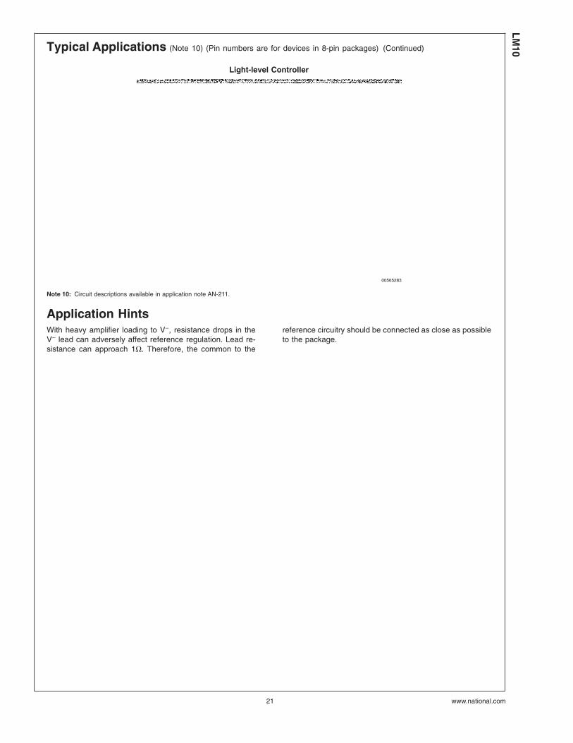
Light-level Controller
00565283
Note 10: Circuit descriptions available in application note AN-211.
Application HintsWith heavy amplifier loading to V−, resistance drops in theV− lead can adversely affect reference regulation. Lead re-sistance can approach 1Ω. Therefore, the common to the
reference circuitry should be connected as close as possibleto the package.
LM10
www.national.com21
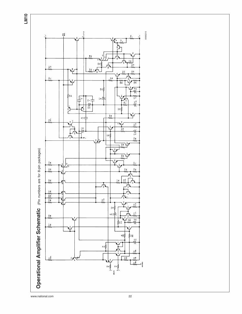
Op
erat
ion
alA
mp
lifie
rS
chem
atic
(Pin
num
bers
are
for
8-pi
npa
ckag
es)
0056
5213
LM10
www.national.com 22
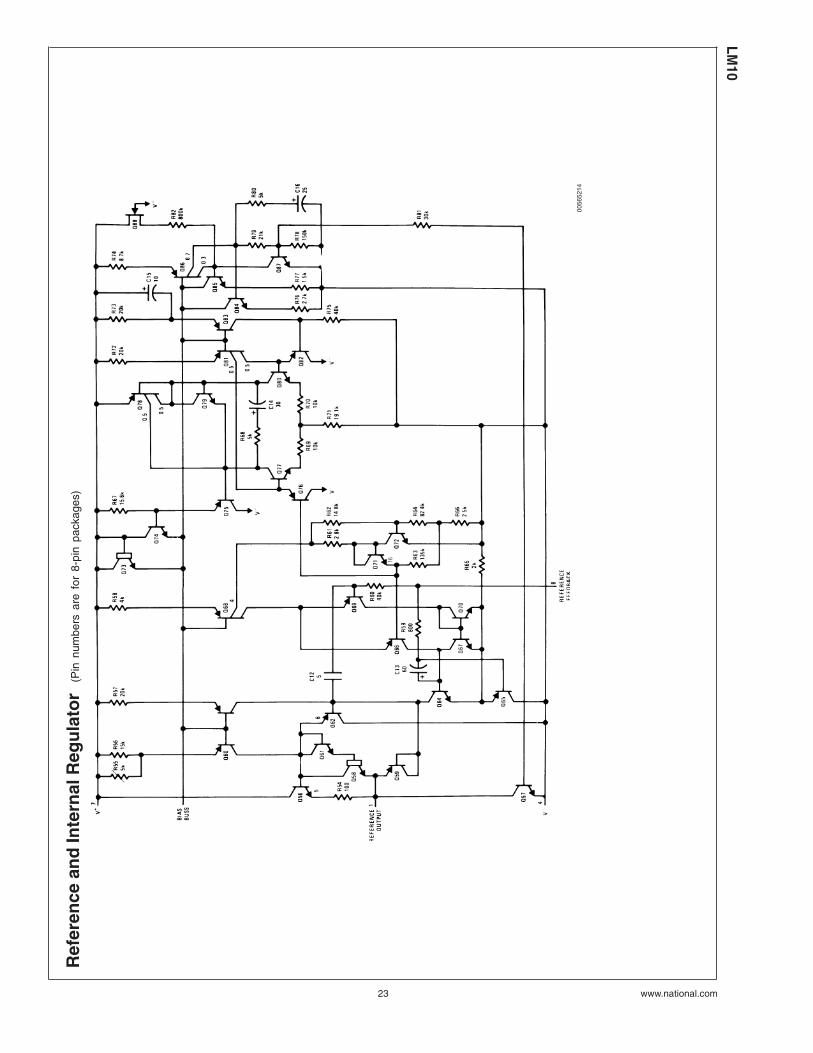
Ref
eren
cean
dIn
tern
alR
egu
lato
r(P
innu
mbe
rsar
efo
r8-
pin
pack
ages
)
0056
5214
LM10
www.national.com23
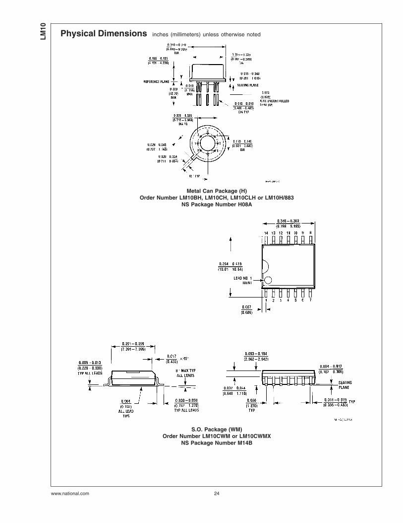
Physical Dimensions inches (millimeters) unless otherwise noted
Metal Can Package (H)Order Number LM10BH, LM10CH, LM10CLH or LM10H/883
NS Package Number H08A
S.O. Package (WM)Order Number LM10CWM or LM10CWMX
NS Package Number M14B
LM10
www.national.com 24
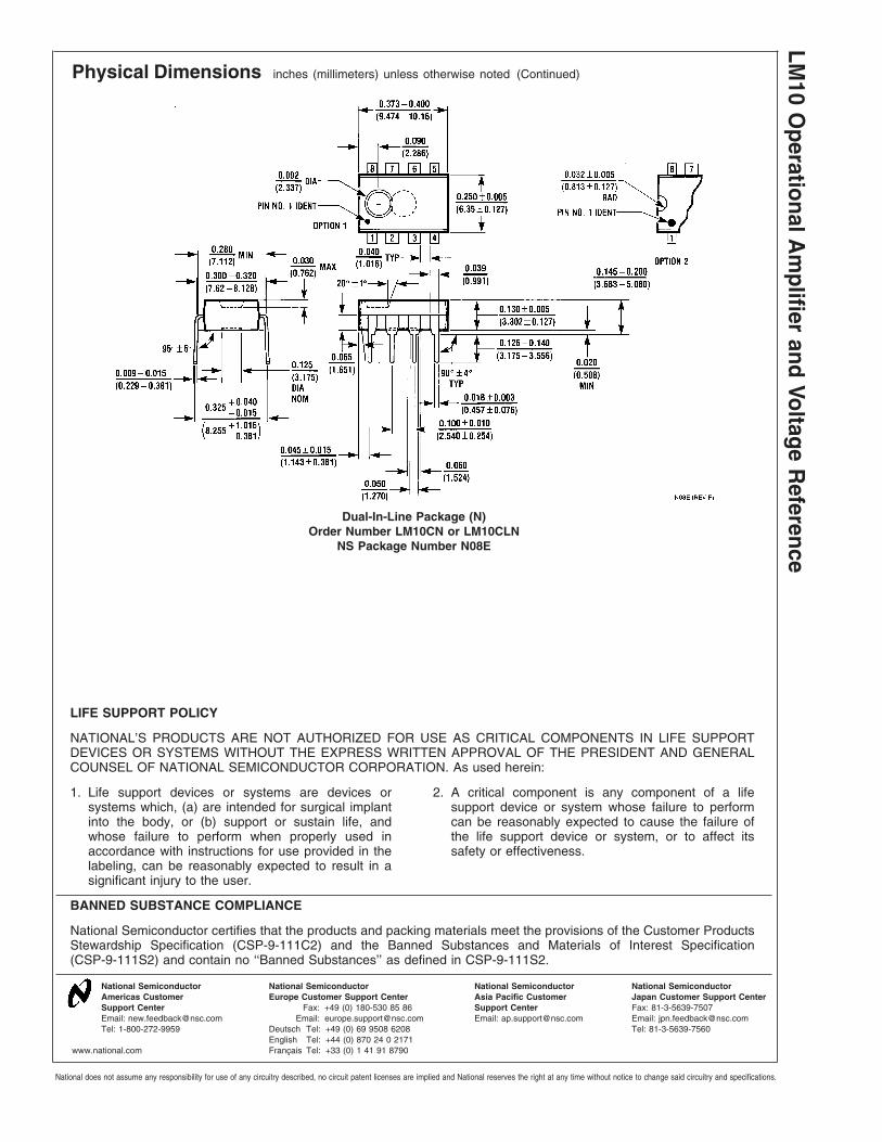
Physical Dimensions inches (millimeters) unless otherwise noted (Continued)
Dual-In-Line Package (N)Order Number LM10CN or LM10CLN
NS Package Number N08E
LIFE SUPPORT POLICY
NATIONAL’S PRODUCTS ARE NOT AUTHORIZED FOR USE AS CRITICAL COMPONENTS IN LIFE SUPPORTDEVICES OR SYSTEMS WITHOUT THE EXPRESS WRITTEN APPROVAL OF THE PRESIDENT AND GENERALCOUNSEL OF NATIONAL SEMICONDUCTOR CORPORATION. As used herein:
1. Life support devices or systems are devices orsystems which, (a) are intended for surgical implantinto the body, or (b) support or sustain life, andwhose failure to perform when properly used inaccordance with instructions for use provided in thelabeling, can be reasonably expected to result in asignificant injury to the user.
2. A critical component is any component of a lifesupport device or system whose failure to performcan be reasonably expected to cause the failure ofthe life support device or system, or to affect itssafety or effectiveness.
BANNED SUBSTANCE COMPLIANCE
National Semiconductor certifies that the products and packing materials meet the provisions of the Customer ProductsStewardship Specification (CSP-9-111C2) and the Banned Substances and Materials of Interest Specification(CSP-9-111S2) and contain no ‘‘Banned Substances’’ as defined in CSP-9-111S2.
National SemiconductorAmericas CustomerSupport CenterEmail: [email protected]: 1-800-272-9959
National SemiconductorEurope Customer Support Center
Fax: +49 (0) 180-530 85 86Email: [email protected]
Deutsch Tel: +49 (0) 69 9508 6208English Tel: +44 (0) 870 24 0 2171Français Tel: +33 (0) 1 41 91 8790
National SemiconductorAsia Pacific CustomerSupport CenterEmail: [email protected]
National SemiconductorJapan Customer Support CenterFax: 81-3-5639-7507Email: [email protected]: 81-3-5639-7560
www.national.com
LM10
OperationalA
mplifier
andVoltage
Reference
National does not assume any responsibility for use of any circuitry described, no circuit patent licenses are implied and National reserves the right at any time without notice to change said circuitry and specifications.