lm10qml operational amplifier and voltage reference … · lm10qml operational amplifier and...
TRANSCRIPT
LM10QML
www.ti.com SNOSAP1A –OCTOBER 2010–REVISED MARCH 2013
LM10QML Operational Amplifier and Voltage ReferenceCheck for Samples: LM10QML
1FEATURES DESCRIPTIONThe LM10 is a monolithic linear IC consisting of a
2• Input Offset Voltage: 2.0 mV (max)precision reference, an adjustable reference buffer
• Input Offset Current: 0.7 nA (max) and an independent, high quality op amp.• Input Bias Current: 20 nA (max)
The unit can operate from a total supply voltage as• Reference Regulation: 0.1% (max) low as 1.1V or as high as 40V, drawing only 270μA.• Offset Voltage Drift: 2μV/°C A complementary output stage swings within 15 mV
of the supply terminals or will deliver ±20 mA output• Reference Drift: 0.002%/°Ccurrent with ±0.4V saturation. Reference output canbe as low as 200 mV.
The circuit is recommended for portable equipmentand is completely specified for operation from asingle power cell. In contrast, high output-drivecapability, both voltage and current, along withthermal overload protection, suggest it in demandinggeneral-purpose applications.
The device is capable of operating in a floating mode,independent of fixed supplies. It can function as aremote comparator, signal conditioner, SCR controlleror transmitter for analog signals, delivering theprocessed signal on the same line used to supplypower. It is also suited for operation in a wide rangeof voltage- and current-regulator applications, fromlow voltages to several hundred volts, providinggreater precision than existing ICs.
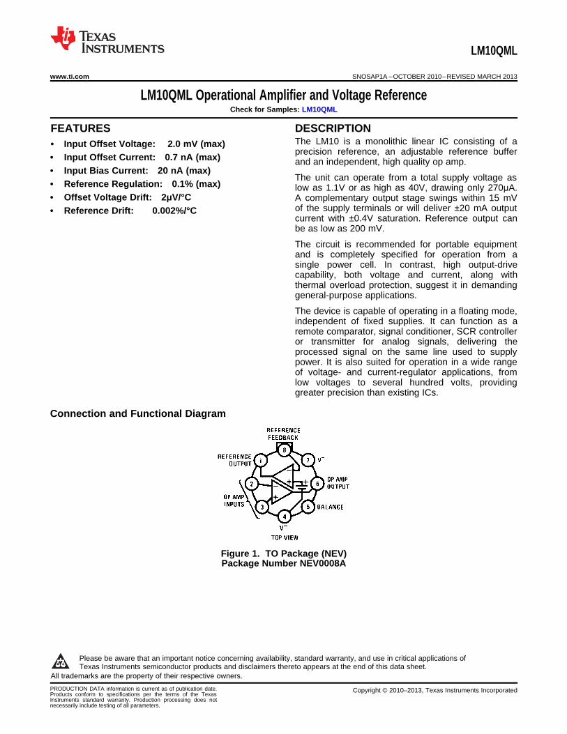
Connection and Functional Diagram
Figure 1. TO Package (NEV)Package Number NEV0008A
1
Please be aware that an important notice concerning availability, standard warranty, and use in critical applications ofTexas Instruments semiconductor products and disclaimers thereto appears at the end of this data sheet.
2All trademarks are the property of their respective owners.
PRODUCTION DATA information is current as of publication date. Copyright © 2010–2013, Texas Instruments IncorporatedProducts conform to specifications per the terms of the TexasInstruments standard warranty. Production processing does notnecessarily include testing of all parameters.

LM10QML
SNOSAP1A –OCTOBER 2010–REVISED MARCH 2013 www.ti.com
Figure 2. Operational Amplifier Schematic — (Pin numbers are for 8-pin packages)
Figure 3. Reference and Internal Regulator Schematic — (Pin numbers are for 8-pin packages)
These devices have limited built-in ESD protection. The leads should be shorted together or the device placed in conductive foamduring storage or handling to prevent electrostatic damage to the MOS gates.
2 Submit Documentation Feedback Copyright © 2010–2013, Texas Instruments Incorporated
Product Folder Links: LM10QML

LM10QML
www.ti.com SNOSAP1A –OCTOBER 2010–REVISED MARCH 2013
Absolute Maximum Ratings (1)
Total Supply Voltage 45V
Differential Input Voltage (2) ±40V
Power Dissipation (PDmax)(3) Internally Limited
Output Short-circuit Duration (4) Continuous
Storage Temperature Range −55°C ≤ TA ≤ +150°C
Maximum Junction Temperature (TJmax) 150°C
Lead Temperature (Soldering 10 seconds) 300°C
Thermal Resistance θJA Still Air 150°C
500LF/Min Air flow 45°C
θJC 45°C
ESD Rating to be determined
(1) Absolute Maximum Ratings indicate limits beyond which damage to the device may occur. Operating Ratings indicate conditions forwhich the device is functional, but do not ensure specific performance limits. For ensured specifications and test conditions, see theElectrical Characteristics. The ensured specifications apply only for the test conditions listed. Some performance characteristics maydegrade when the device is not operated under the listed test conditions.
(2) The Input voltage can exceed the supply voltages provided that the voltage from the input to any other terminal does not exceed themaximum differential input voltage and excess dissipation is accounted for when VI< VS
-.(3) The maximum power dissipation must be derated at elevated temperatures and is dictated by TJmax (maximum junction temperature),
θJA (package junction to ambient thermal resistance), and TA (ambient temperature). The maximum allowable power dissipation at anytemperature is PDmax = (TJmax - TA)/θJA or the number given in the Absolute Maximum Ratings, whichever is lower..
(4) Internal thermal limiting prevents excessive heating that could result in sudden failure, but the IC can be subjected to accelerated stresswith a shorted output and worst-case conditions.
Quality Conformance InspectionMil-Std-883, Method 5005 - Group A
Subgroup Description Temp °C
1 Static tests at +25
2 Static tests at +125
3 Static tests at -55
4 Dynamic tests at +25
5 Dynamic tests at +125
6 Dynamic tests at -55
7 Functional tests at +25
8A Functional tests at +125
8B Functional tests at -55
9 Switching tests at +25
10 Switching tests at +125
11 Switching tests at -55
12 Settling time at +25
13 Settling time at +125
14 Settling time at -55
Copyright © 2010–2013, Texas Instruments Incorporated Submit Documentation Feedback 3
Product Folder Links: LM10QML

LM10QML
SNOSAP1A –OCTOBER 2010–REVISED MARCH 2013 www.ti.com
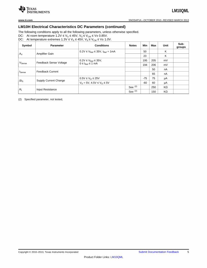
LM10H Electrical Characteristics DC ParametersThe following conditions apply to all the following parameters, unless otherwise specified.DC: At room temperature 1.2V ≤ VS ≤ 45V, VS
-≤ VCM ≤ V± 0.85V.DC: At temperature extremes 1.3V ≤ VS ≤ 45V, VS
-≤ VCM ≤ V± 1.0V.
Sub-Symbol Parameter Conditions Notes Min Max Unit groups
-2.0 2.0 mV 1IO = 0mA
-3.0 3.0 mV 2, 3
VS = 1.2V, IO = ±2mA -3.0 3.0 mV 1VIO Input Offset Voltage
VS = 1.3V, IO = ±2mA -4.0 4.0 mV 2, 3
VS = 4V, IO = ±20mA -3.0 3.0 mV 1
VS = 4V, IO = ±15mA -4.0 4.0 mV 2, 3
-0.7 0.7 nA 1IIO Input Offset Current
-1.5 1.5 nA 2, 3
20 nA 1IIB Input Bias Current
30 nA 2, 3
93 dB 1CMRR Common Mode Rejection VS = 45V, -20V ≤ VCM ≤ 24.2V
87 dB 2, 3
VS+ = 0.85V, 90 dB 1-0.35V ≥ VS
-≥ -44.2V
VS+ = 1V, 84 dB 2, 3-0.3V ≥ VS
-≥ -44.2VPSRR Supply Voltage Rejection
0.85V ≤ VS+ ≤ 44.6V, 96 dB 1VS
-= -0.35V
1V ≤ VS+ ≤ 44.6V, 90 dB 2, 3VS
-= -0.3V
VRLine 91 dB 1Line Regulation IRef = 1mA
85 dB 2, 3
VS = 1.2V, 0 ≤ IO ≤ 1mA 60 dB 1VRLoad Load Regulation
VS = 1.3V, 0 ≤ IO ≤ 1mA 57 dB 2, 3
400 µA 1IS Supply Current
500 µA 2, 3
VS = ±20V, IO = 0A, 120 K 4VO = ± 19.95V 80 K 5, 6
VS = ±2V, IO = ±20mA, 5.0 K 4VO = ±1.4V
VS = ±2V, IO = ±15mA, 1.5 K 5, 6VO = ±1.4VAV Large Signal Voltage GainVS
+ = 0.85V, VCM = -0.25V 1.5 K 4VS
-= -0.35V, IO = ±2mA,-0.15V ≤ VO ≤ 0.65V,
VS+ = 1V, VCM = -0.35V 0.5 K 5, 6
VS-= -0.3V, IO = ±2mA,
+0.05V ≤ VO ≤ 0.65V,
1.1V ≤ VOUT ≤ 6.1V, See (1) 14 K 4-5mA ≤ IOUT ≤ -0.1mA
1.2V ≤ VOUT ≤ 6.2V, See (1) 6.0 K 5, 6-5mA ≤ IOUT ≤ -0.1mAAVSH Shunt Gain
1.4V ≤ VOUT ≤ 6.4V, See (1) 8.0 K 4-5mA ≤ IOUT ≤ -0.1mA
1.4V ≤ VOUT ≤ 6.4V, See (1) 4.0 K 5, 6-20mA ≤ IOUT ≤ -0.1mA
(1) This defines operation in floating applications such as the bootstrapped regulator or two-wire transmitter. Output is connected to the VS+
terminal of the IC and input common mode is referred to VS-(see Typical Applications -). Effect of larger output-voltage swings with
higher load resistance can be accounted for by adding the positive-supply rejection error.
4 Submit Documentation Feedback Copyright © 2010–2013, Texas Instruments Incorporated
Product Folder Links: LM10QML
LM10QML
www.ti.com SNOSAP1A –OCTOBER 2010–REVISED MARCH 2013
LM10H Electrical Characteristics DC Parameters (continued)The following conditions apply to all the following parameters, unless otherwise specified.DC: At room temperature 1.2V ≤ VS ≤ 45V, VS
-≤ VCM ≤ V± 0.85V.DC: At temperature extremes 1.3V ≤ VS ≤ 45V, VS
-≤ VCM ≤ V± 1.0V.
Sub-Symbol Parameter Conditions Notes Min Max Unit groups
0.2V ≤ VRef ≤ 35V, IRef = 1mA 50 KAV Amplifier Gain
23 K
0.2V ≤ VRef ≤ 35V, 195 205 mVVSense Feedback Sense Voltage 0 ≤ IRef ≤ 1 mA 194 206 mV
50 nAISense Feedback Current
65 nA
0.5V ≤ VO ≤ 25V -75 75 µAΔIS Supply Current Change
VS = 5V, 4.5V ≤ VO ≤ 5V -60 60 µA
See (2) 250 KΩRI Input Resistance
See (2) 150 KΩ
(2) Specified parameter, not tested,
Copyright © 2010–2013, Texas Instruments Incorporated Submit Documentation Feedback 5
Product Folder Links: LM10QML
LM10QML
SNOSAP1A –OCTOBER 2010–REVISED MARCH 2013 www.ti.com
Definition of Terms
Input offset voltage:That voltage which must be applied between the input terminals to bias the unloadedoutput in the linear region.
Input offset current:The difference in the currents at the input terminals when the unloaded output is in thelinear region.
Input bias current:The absolute value of the average of the two input currents.
Input resistance:The ratio of the change in input voltage to the change in input current on either input with theother grounded.
Large signal voltage gain:The ratio of the specified output voltage swing to the change in differential inputvoltage required to produce it.
Shunt gain:The ratio of the specified output voltage swing to the change in differential input voltage required toproduce it with the output tied to the VS
+ terminal of the IC. The load and power source are connectedbetween the VS
+ and VS-terminals, and input common-mode is referred to the VS
-terminal.
Common-mode rejection:The ratio of the input voltage range to the change in offset voltage between theextremes.
Supply-voltage rejection:The ratio of the specified supply-voltage change to the change in offset voltagebetween the extremes.
Line regulation:The average change in reference output voltage over the specified supply voltage range.
Load regulation:The change in reference output voltage from no load to that load specified.
Feedback sense voltage:The voltage, referred to VS-, on the reference feedback terminal while operating in
regulation.
Reference amplifier gain:The ratio of the specified reference output change to the change in feedback sensevoltage required to produce it.
Feedback current:The absolute value of the current at the feedback terminal when operating in regulation.
Supply current:The current required from the power source to operate the amplifier and reference with theiroutputs unloaded and operating in the linear range.
6 Submit Documentation Feedback Copyright © 2010–2013, Texas Instruments Incorporated
Product Folder Links: LM10QML
LM10QML
www.ti.com SNOSAP1A –OCTOBER 2010–REVISED MARCH 2013
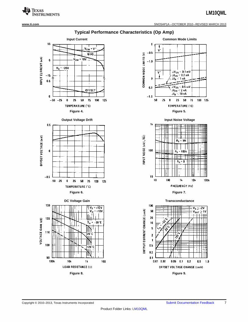
Typical Performance Characteristics (Op Amp)
Input Current Common Mode Limits
Figure 4. Figure 5.
Output Voltage Drift Input Noise Voltage
Figure 6. Figure 7.
DC Voltage Gain Transconductance
Figure 8. Figure 9.
Copyright © 2010–2013, Texas Instruments Incorporated Submit Documentation Feedback 7
Product Folder Links: LM10QML
LM10QML
SNOSAP1A –OCTOBER 2010–REVISED MARCH 2013 www.ti.com
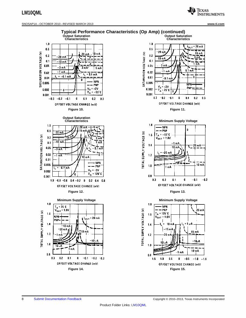
Typical Performance Characteristics (Op Amp) (continued)Output Saturation Output Saturation
Characteristics Characteristics
Figure 10. Figure 11.
Output SaturationCharacteristics Minimum Supply Voltage
Figure 12. Figure 13.
Minimum Supply Voltage Minimum Supply Voltage
Figure 14. Figure 15.
8 Submit Documentation Feedback Copyright © 2010–2013, Texas Instruments Incorporated
Product Folder Links: LM10QML
LM10QML
www.ti.com SNOSAP1A –OCTOBER 2010–REVISED MARCH 2013
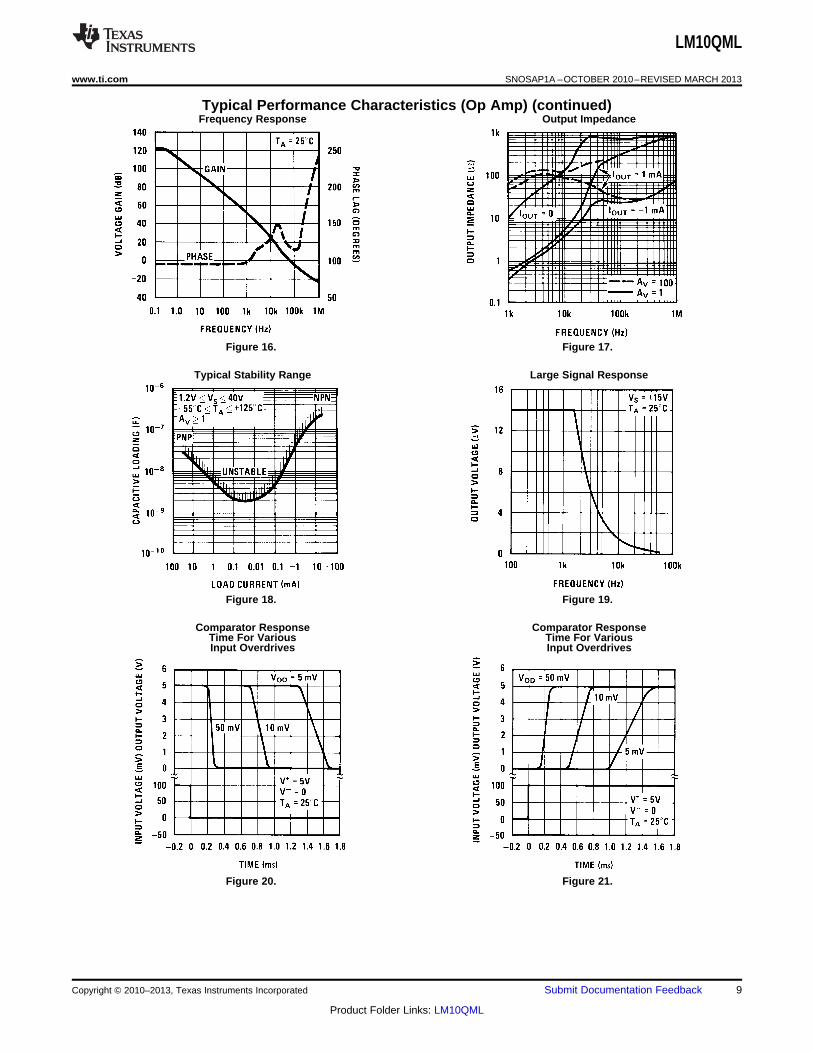
Typical Performance Characteristics (Op Amp) (continued)Frequency Response Output Impedance
Figure 16. Figure 17.
Typical Stability Range Large Signal Response
Figure 18. Figure 19.
Comparator Response Comparator ResponseTime For Various Time For VariousInput Overdrives Input Overdrives
Figure 20. Figure 21.
Copyright © 2010–2013, Texas Instruments Incorporated Submit Documentation Feedback 9
Product Folder Links: LM10QML
LM10QML
SNOSAP1A –OCTOBER 2010–REVISED MARCH 2013 www.ti.com
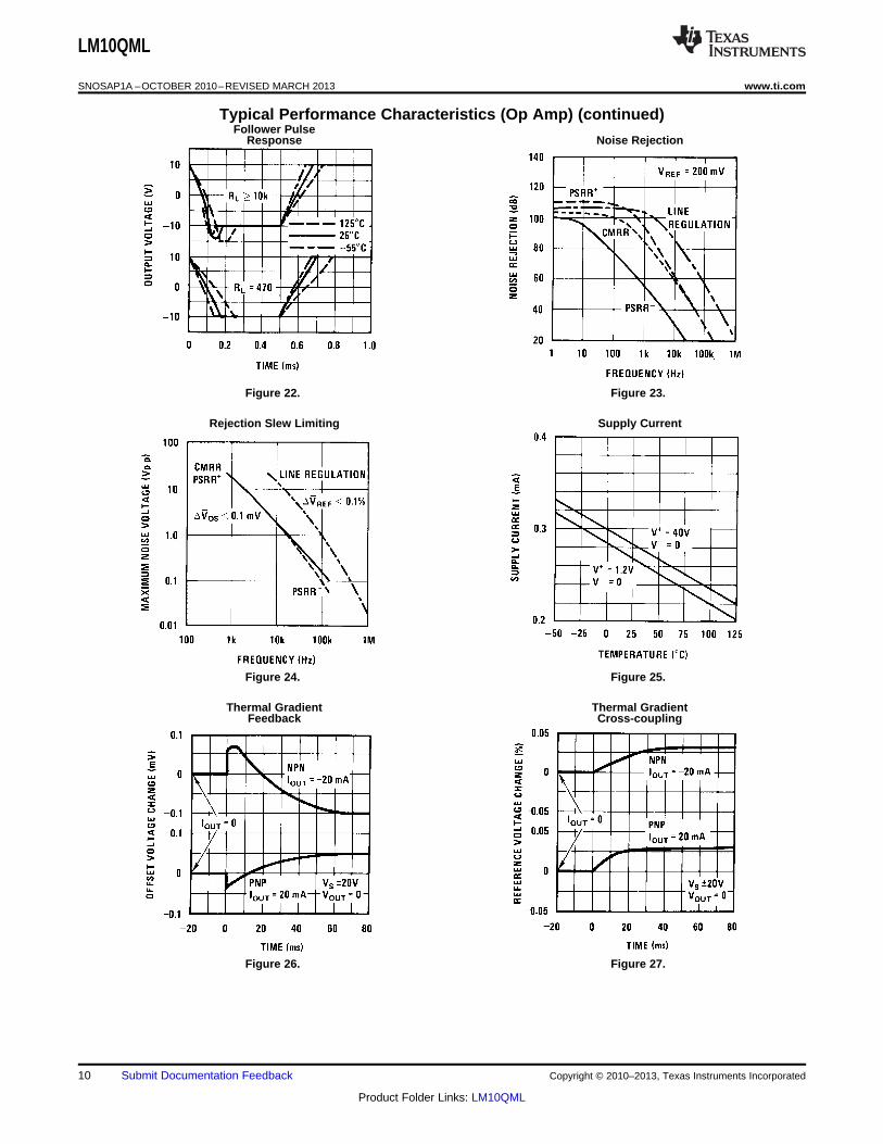
Typical Performance Characteristics (Op Amp) (continued)Follower Pulse
Response Noise Rejection
Figure 22. Figure 23.
Rejection Slew Limiting Supply Current
Figure 24. Figure 25.
Thermal Gradient Thermal GradientFeedback Cross-coupling
Figure 26. Figure 27.
10 Submit Documentation Feedback Copyright © 2010–2013, Texas Instruments Incorporated
Product Folder Links: LM10QML

LM10QML
www.ti.com SNOSAP1A –OCTOBER 2010–REVISED MARCH 2013
Typical Performance Characteristics (Op Amp) (continued)Shunt Gain Shunt Gain
Figure 28. Figure 29.
Shunt Gain Shunt Gain
Figure 30. Figure 31.
Shunt Gain Shunt Gain
Figure 32. Figure 33.
Copyright © 2010–2013, Texas Instruments Incorporated Submit Documentation Feedback 11
Product Folder Links: LM10QML
LM10QML
SNOSAP1A –OCTOBER 2010–REVISED MARCH 2013 www.ti.com
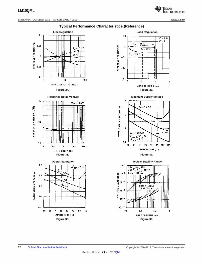
Typical Performance Characteristics (Reference)
Line Regulation Load Regulation
Figure 34. Figure 35.
Reference Noise Voltage Minimum Supply Voltage
Figure 36. Figure 37.
Output Saturation Typical Stability Range
Figure 38. Figure 39.
12 Submit Documentation Feedback Copyright © 2010–2013, Texas Instruments Incorporated
Product Folder Links: LM10QML
LM10QML
www.ti.com SNOSAP1A –OCTOBER 2010–REVISED MARCH 2013
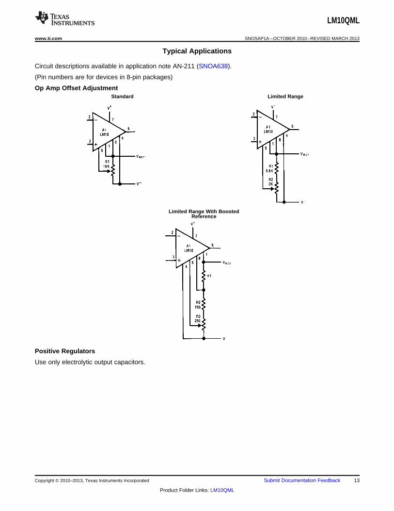
Typical Applications
Circuit descriptions available in application note AN-211 (SNOA638).
(Pin numbers are for devices in 8-pin packages)
Op Amp Offset AdjustmentStandard Limited Range
Limited Range With BoostedReference
Positive Regulators
Use only electrolytic output capacitors.
Copyright © 2010–2013, Texas Instruments Incorporated Submit Documentation Feedback 13
Product Folder Links: LM10QML

LM10QML
SNOSAP1A –OCTOBER 2010–REVISED MARCH 2013 www.ti.com
Low Voltage Best Regulation
Zero Output
Use only electrolytic output capacitors.
Current Regulator Shunt Regulator
Required For Capacitive Loading
14 Submit Documentation Feedback Copyright © 2010–2013, Texas Instruments Incorporated
Product Folder Links: LM10QML
LM10QML
www.ti.com SNOSAP1A –OCTOBER 2010–REVISED MARCH 2013
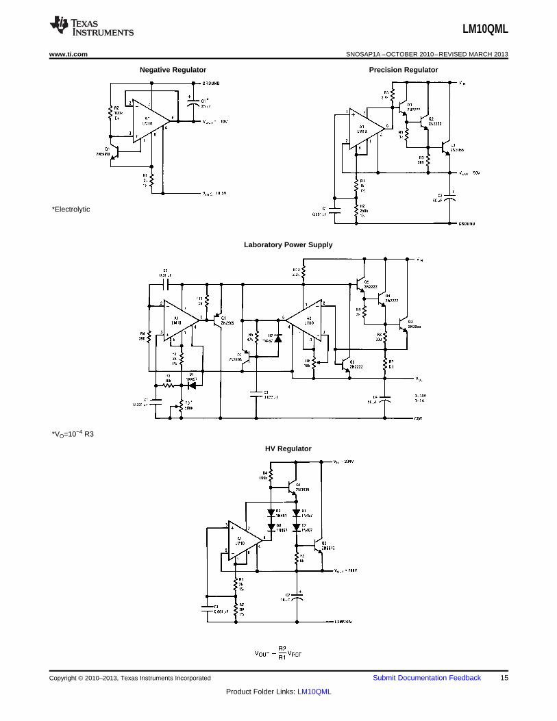
Negative Regulator Precision Regulator
*Electrolytic
Laboratory Power Supply
*VO=10−4 R3
HV Regulator
Copyright © 2010–2013, Texas Instruments Incorporated Submit Documentation Feedback 15
Product Folder Links: LM10QML
LM10QML
SNOSAP1A –OCTOBER 2010–REVISED MARCH 2013 www.ti.com
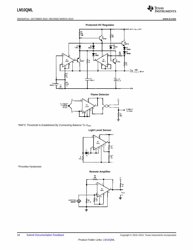
Protected HV Regulator
Flame Detector
*800°C Threshold Is Established By Connecting Balance To VRef.
Light Level Sensor
*Provides Hysteresis
Remote Amplifier
16 Submit Documentation Feedback Copyright © 2010–2013, Texas Instruments Incorporated
Product Folder Links: LM10QML
LM10QML
www.ti.com SNOSAP1A –OCTOBER 2010–REVISED MARCH 2013
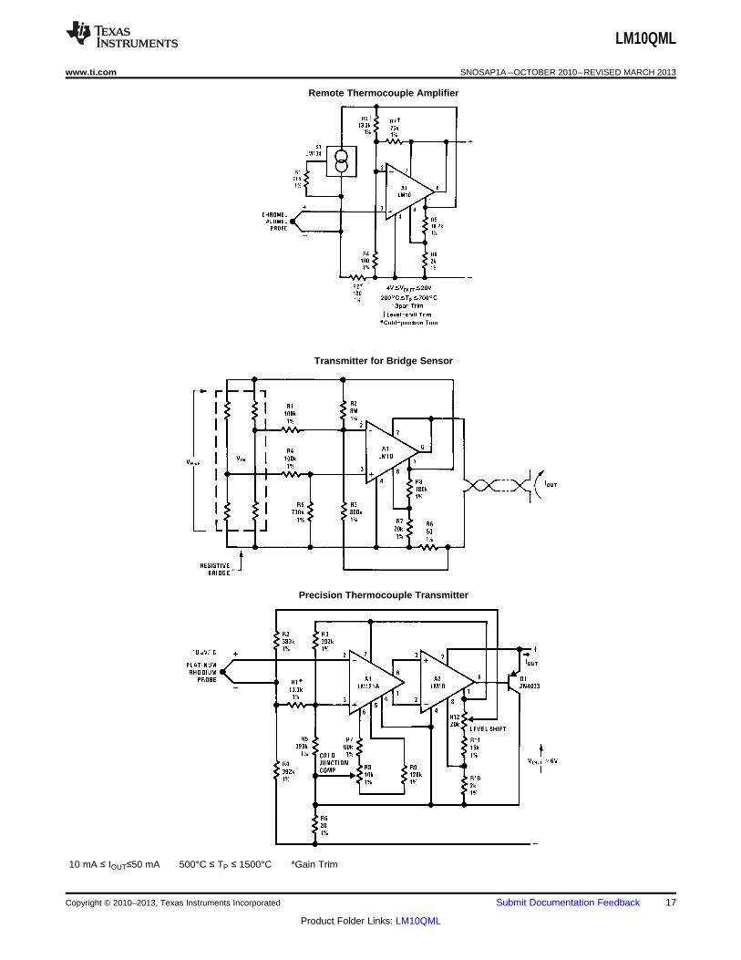
Remote Thermocouple Amplifier
Transmitter for Bridge Sensor
Precision Thermocouple Transmitter
10 mA ≤ IOUT≤50 mA 500°C ≤ TP ≤ 1500°C *Gain Trim
Copyright © 2010–2013, Texas Instruments Incorporated Submit Documentation Feedback 17
Product Folder Links: LM10QML

LM10QML
SNOSAP1A –OCTOBER 2010–REVISED MARCH 2013 www.ti.com
Resistance Thermometer Transmitter
Optical Pyrometer
††Level-shift Trim*Scale Factor Trim†Copper Wire Wound
18 Submit Documentation Feedback Copyright © 2010–2013, Texas Instruments Incorporated
Product Folder Links: LM10QML
LM10QML
www.ti.com SNOSAP1A –OCTOBER 2010–REVISED MARCH 2013
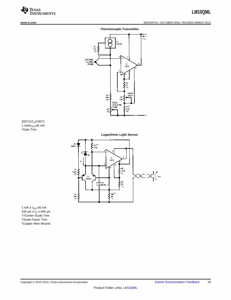
Thermocouple Transmitter
200°C≤Tp≤700°C1 mA≤IOUT≤5 mA†Gain Trim
Logarithmic Light Sensor
1 mA ≤ IOUT≤5 mA‡50 μA ≤ ID ≤ 500 μA††Center Scale Trim†Scale Factor Trim*Copper Wire Wound
Copyright © 2010–2013, Texas Instruments Incorporated Submit Documentation Feedback 19
Product Folder Links: LM10QML
LM10QML
SNOSAP1A –OCTOBER 2010–REVISED MARCH 2013 www.ti.com
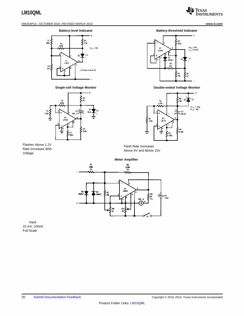
Battery-level Indicator Battery-threshold Indicator
Single-cell Voltage Monitor Double-ended Voltage Monitor
Flashes Above 1.2V Flash Rate IncreasesRate Increases With Above 6V and Below 15VVoltage
Meter Amplifier
Input10 mV, 100nAFull-Scale
20 Submit Documentation Feedback Copyright © 2010–2013, Texas Instruments Incorporated
Product Folder Links: LM10QML
LM10QML
www.ti.com SNOSAP1A –OCTOBER 2010–REVISED MARCH 2013
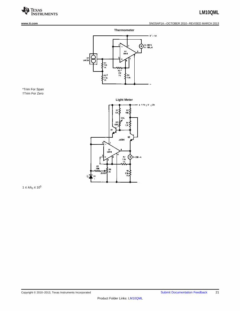
Thermometer
*Trim For Span†Trim For Zero
Light Meter
1 ≤ λ/λ0 ≤ 105
Copyright © 2010–2013, Texas Instruments Incorporated Submit Documentation Feedback 21
Product Folder Links: LM10QML

LM10QML
SNOSAP1A –OCTOBER 2010–REVISED MARCH 2013 www.ti.com
Microphone Amplifier
ZOUT∼680Ω @ 5 kHzAV ≤ 1kf1∼100 Hzf2∼5 kHzRL∼500*Max Gain Trim
Isolated Voltage Sensor
†Controls “Loop Gain”*Optional Frequency Shaping
22 Submit Documentation Feedback Copyright © 2010–2013, Texas Instruments Incorporated
Product Folder Links: LM10QML
LM10QML
www.ti.com SNOSAP1A –OCTOBER 2010–REVISED MARCH 2013
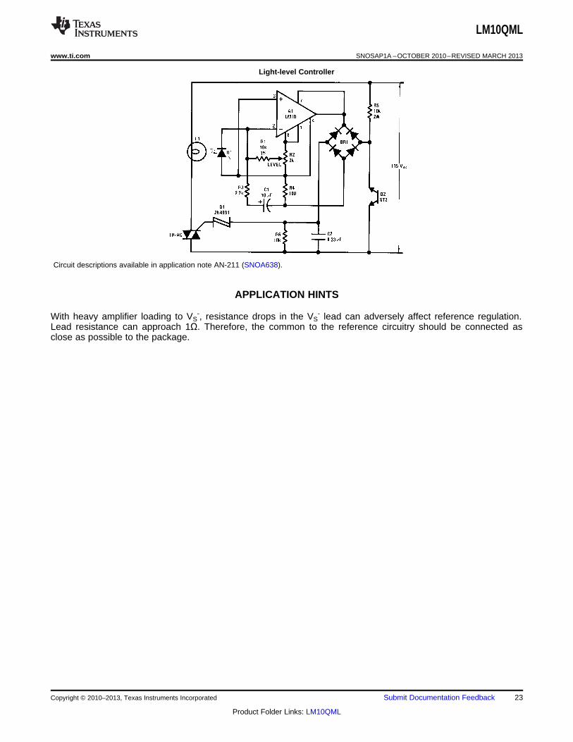
Light-level Controller
Circuit descriptions available in application note AN-211 (SNOA638).
APPLICATION HINTS
With heavy amplifier loading to VS-, resistance drops in the VS
- lead can adversely affect reference regulation.Lead resistance can approach 1Ω. Therefore, the common to the reference circuitry should be connected asclose as possible to the package.
Copyright © 2010–2013, Texas Instruments Incorporated Submit Documentation Feedback 23
Product Folder Links: LM10QML
LM10QML
SNOSAP1A –OCTOBER 2010–REVISED MARCH 2013 www.ti.com
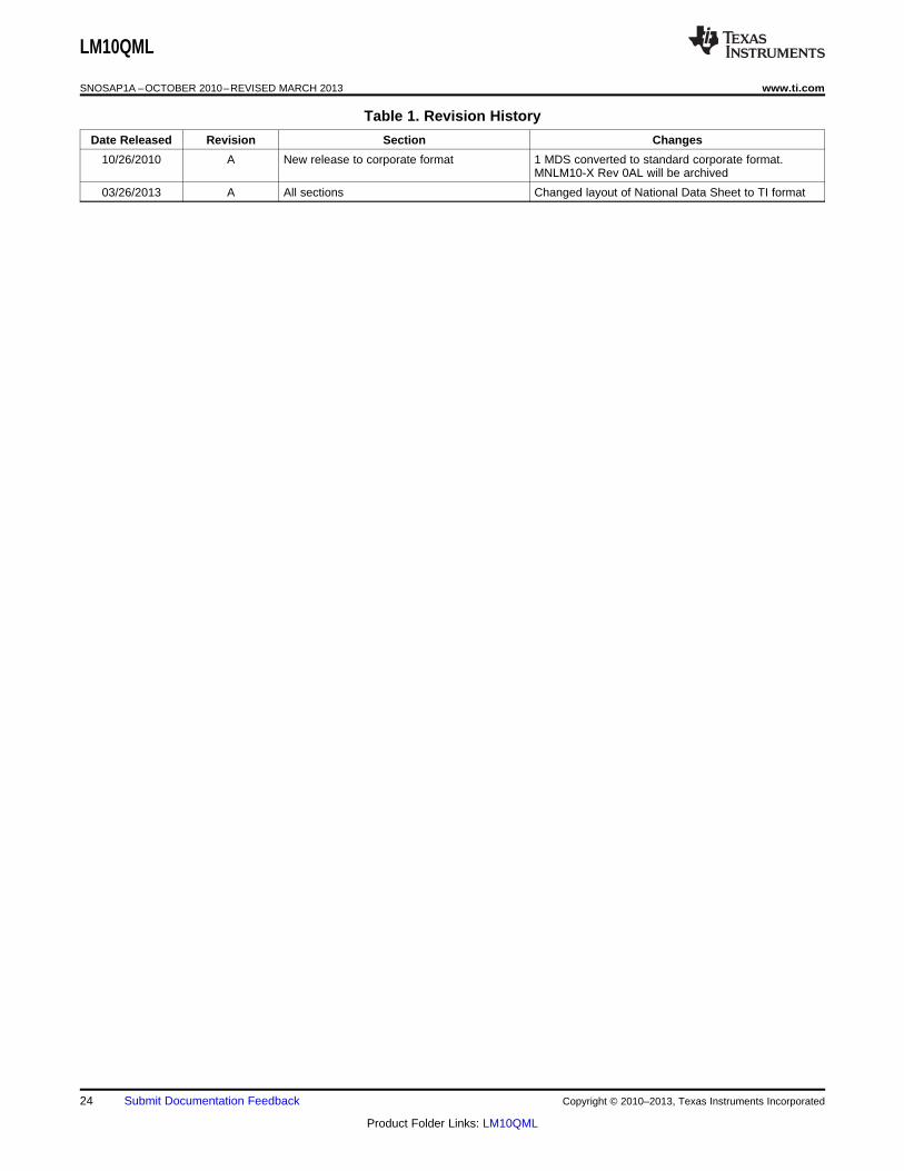
Table 1. Revision History
Date Released Revision Section Changes
10/26/2010 A New release to corporate format 1 MDS converted to standard corporate format.MNLM10-X Rev 0AL will be archived
03/26/2013 A All sections Changed layout of National Data Sheet to TI format
24 Submit Documentation Feedback Copyright © 2010–2013, Texas Instruments Incorporated
Product Folder Links: LM10QML
PACKAGE OPTION ADDENDUM
www.ti.com 25-Oct-2016
Addendum-Page 1
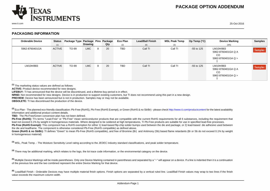
PACKAGING INFORMATION
Orderable Device Status(1)
Package Type PackageDrawing
Pins PackageQty
Eco Plan(2)
Lead/Ball Finish(6)
MSL Peak Temp(3)
Op Temp (°C) Device Marking(4/5)
Samples
5962-8760401GA ACTIVE TO-99 LMC 8 20 TBD Call TI Call TI -55 to 125 LM10H/8835962-8760401GA Q A CO5962-8760401GA Q > T
LM10H/883 ACTIVE TO-99 LMC 8 20 TBD Call TI Call TI -55 to 125 LM10H/8835962-8760401GA Q A CO5962-8760401GA Q > T
(1) The marketing status values are defined as follows:ACTIVE: Product device recommended for new designs.LIFEBUY: TI has announced that the device will be discontinued, and a lifetime-buy period is in effect.NRND: Not recommended for new designs. Device is in production to support existing customers, but TI does not recommend using this part in a new design.PREVIEW: Device has been announced but is not in production. Samples may or may not be available.OBSOLETE: TI has discontinued the production of the device.
(2) Eco Plan - The planned eco-friendly classification: Pb-Free (RoHS), Pb-Free (RoHS Exempt), or Green (RoHS & no Sb/Br) - please check http://www.ti.com/productcontent for the latest availabilityinformation and additional product content details.TBD: The Pb-Free/Green conversion plan has not been defined.Pb-Free (RoHS): TI's terms "Lead-Free" or "Pb-Free" mean semiconductor products that are compatible with the current RoHS requirements for all 6 substances, including the requirement thatlead not exceed 0.1% by weight in homogeneous materials. Where designed to be soldered at high temperatures, TI Pb-Free products are suitable for use in specified lead-free processes.Pb-Free (RoHS Exempt): This component has a RoHS exemption for either 1) lead-based flip-chip solder bumps used between the die and package, or 2) lead-based die adhesive used betweenthe die and leadframe. The component is otherwise considered Pb-Free (RoHS compatible) as defined above.Green (RoHS & no Sb/Br): TI defines "Green" to mean Pb-Free (RoHS compatible), and free of Bromine (Br) and Antimony (Sb) based flame retardants (Br or Sb do not exceed 0.1% by weightin homogeneous material)
(3) MSL, Peak Temp. - The Moisture Sensitivity Level rating according to the JEDEC industry standard classifications, and peak solder temperature.
(4) There may be additional marking, which relates to the logo, the lot trace code information, or the environmental category on the device.
(5) Multiple Device Markings will be inside parentheses. Only one Device Marking contained in parentheses and separated by a "~" will appear on a device. If a line is indented then it is a continuationof the previous line and the two combined represent the entire Device Marking for that device.
(6) Lead/Ball Finish - Orderable Devices may have multiple material finish options. Finish options are separated by a vertical ruled line. Lead/Ball Finish values may wrap to two lines if the finishvalue exceeds the maximum column width.

PACKAGE OPTION ADDENDUM
www.ti.com 25-Oct-2016
Addendum-Page 2
Important Information and Disclaimer:The information provided on this page represents TI's knowledge and belief as of the date that it is provided. TI bases its knowledge and belief on informationprovided by third parties, and makes no representation or warranty as to the accuracy of such information. Efforts are underway to better integrate information from third parties. TI has taken andcontinues to take reasonable steps to provide representative and accurate information but may not have conducted destructive testing or chemical analysis on incoming materials and chemicals.TI and TI suppliers consider certain information to be proprietary, and thus CAS numbers and other limited information may not be available for release.
In no event shall TI's liability arising out of such information exceed the total purchase price of the TI part(s) at issue in this document sold by TI to Customer on an annual basis.

IMPORTANT NOTICE
Texas Instruments Incorporated and its subsidiaries (TI) reserve the right to make corrections, enhancements, improvements and otherchanges to its semiconductor products and services per JESD46, latest issue, and to discontinue any product or service per JESD48, latestissue. Buyers should obtain the latest relevant information before placing orders and should verify that such information is current andcomplete. All semiconductor products (also referred to herein as “components”) are sold subject to TI’s terms and conditions of salesupplied at the time of order acknowledgment.TI warrants performance of its components to the specifications applicable at the time of sale, in accordance with the warranty in TI’s termsand conditions of sale of semiconductor products. Testing and other quality control techniques are used to the extent TI deems necessaryto support this warranty. Except where mandated by applicable law, testing of all parameters of each component is not necessarilyperformed.TI assumes no liability for applications assistance or the design of Buyers’ products. Buyers are responsible for their products andapplications using TI components. To minimize the risks associated with Buyers’ products and applications, Buyers should provideadequate design and operating safeguards.TI does not warrant or represent that any license, either express or implied, is granted under any patent right, copyright, mask work right, orother intellectual property right relating to any combination, machine, or process in which TI components or services are used. Informationpublished by TI regarding third-party products or services does not constitute a license to use such products or services or a warranty orendorsement thereof. Use of such information may require a license from a third party under the patents or other intellectual property of thethird party, or a license from TI under the patents or other intellectual property of TI.Reproduction of significant portions of TI information in TI data books or data sheets is permissible only if reproduction is without alterationand is accompanied by all associated warranties, conditions, limitations, and notices. TI is not responsible or liable for such altereddocumentation. Information of third parties may be subject to additional restrictions.Resale of TI components or services with statements different from or beyond the parameters stated by TI for that component or servicevoids all express and any implied warranties for the associated TI component or service and is an unfair and deceptive business practice.TI is not responsible or liable for any such statements.Buyer acknowledges and agrees that it is solely responsible for compliance with all legal, regulatory and safety-related requirementsconcerning its products, and any use of TI components in its applications, notwithstanding any applications-related information or supportthat may be provided by TI. Buyer represents and agrees that it has all the necessary expertise to create and implement safeguards whichanticipate dangerous consequences of failures, monitor failures and their consequences, lessen the likelihood of failures that might causeharm and take appropriate remedial actions. Buyer will fully indemnify TI and its representatives against any damages arising out of the useof any TI components in safety-critical applications.In some cases, TI components may be promoted specifically to facilitate safety-related applications. With such components, TI’s goal is tohelp enable customers to design and create their own end-product solutions that meet applicable functional safety standards andrequirements. Nonetheless, such components are subject to these terms.No TI components are authorized for use in FDA Class III (or similar life-critical medical equipment) unless authorized officers of the partieshave executed a special agreement specifically governing such use.Only those TI components which TI has specifically designated as military grade or “enhanced plastic” are designed and intended for use inmilitary/aerospace applications or environments. Buyer acknowledges and agrees that any military or aerospace use of TI componentswhich have not been so designated is solely at the Buyer's risk, and that Buyer is solely responsible for compliance with all legal andregulatory requirements in connection with such use.TI has specifically designated certain components as meeting ISO/TS16949 requirements, mainly for automotive use. In any case of use ofnon-designated products, TI will not be responsible for any failure to meet ISO/TS16949.
Products ApplicationsAudio www.ti.com/audio Automotive and Transportation www.ti.com/automotiveAmplifiers amplifier.ti.com Communications and Telecom www.ti.com/communicationsData Converters dataconverter.ti.com Computers and Peripherals www.ti.com/computersDLP® Products www.dlp.com Consumer Electronics www.ti.com/consumer-appsDSP dsp.ti.com Energy and Lighting www.ti.com/energyClocks and Timers www.ti.com/clocks Industrial www.ti.com/industrialInterface interface.ti.com Medical www.ti.com/medicalLogic logic.ti.com Security www.ti.com/securityPower Mgmt power.ti.com Space, Avionics and Defense www.ti.com/space-avionics-defenseMicrocontrollers microcontroller.ti.com Video and Imaging www.ti.com/videoRFID www.ti-rfid.comOMAP Applications Processors www.ti.com/omap TI E2E Community e2e.ti.comWireless Connectivity www.ti.com/wirelessconnectivity
Mailing Address: Texas Instruments, Post Office Box 655303, Dallas, Texas 75265Copyright © 2016, Texas Instruments Incorporated