lm1577/lm2577 simple switcher step-upvoltage regulator• soft-startfunction reduces in-rushcurrent...
TRANSCRIPT

LM1577, LM2577
www.ti.com SNOS658D –JUNE 1999–REVISED APRIL 2013
LM1577/LM2577 SIMPLE SWITCHER® Step-Up Voltage RegulatorCheck for Samples: LM1577, LM2577
1FEATURES DESCRIPTIONThe LM1577/LM2577 are monolithic integrated
23• Requires Few External Componentscircuits that provide all of the power and control
• NPN Output Switches 3.0A, can Stand off 65V functions for step-up (boost), flyback, and forward• Wide Input Voltage Range: 3.5V to 40V converter switching regulators. The device is
available in three different output voltage versions:• Current-mode Operation for Improved12V, 15V, and adjustable.Transient Response, Line Regulation, and
Current Limit Requiring a minimum number of externalcomponents, these regulators are cost effective, and• 52 kHz Internal Oscillatorsimple to use. Listed in this data sheet are a family of• Soft-start Function Reduces In-rush Currentstandard inductors and flyback transformers designedDuring Start-up to work with these switching regulators.
• Output Switch Protected by Current Limit,Included on the chip is a 3.0A NPN switch and itsUnder-voltage Lockout, and Thermalassociated protection circuitry, consisting of currentShutdownand thermal limiting, and undervoltage lockout. Otherfeatures include a 52 kHz fixed-frequency oscillator
TYPICAL APPLICATIONS that requires no external components, a soft startmode to reduce in-rush current during start-up, and• Simple Boost Regulatorcurrent mode control for improved rejection of input• Flyback and Forward Regulatorsvoltage and output load transients.
• Multiple-output Regulator
Connection Diagrams
Figure 1. 5-Lead (Straight Leads) TO-220 (T) – Top Figure 2. 5-Lead (Bent, Staggered Leads) TO-220View (T) – Top View
See Package Number KC See Package Number NDH0005D
1
Please be aware that an important notice concerning availability, standard warranty, and use in critical applications ofTexas Instruments semiconductor products and disclaimers thereto appears at the end of this data sheet.
2SIMPLE SWITCHER is a registered trademark of Texas Instruments.3All other trademarks are the property of their respective owners.
PRODUCTION DATA information is current as of publication date. Copyright © 1999–2013, Texas Instruments IncorporatedProducts conform to specifications per the terms of the TexasInstruments standard warranty. Production processing does notnecessarily include testing of all parameters.

LM1577, LM2577
SNOS658D –JUNE 1999–REVISED APRIL 2013 www.ti.com
*No Internal Connection
*No internal Connection
Figure 3. 16-Lead PDIP (N) – Top View Figure 4. 24-Lead SOIC Package (M) – Top ViewSee Package Number NBG0016G See Package Number DW
Figure 5. 5-Lead DDPAK/TO-263 (S) SFM Package – Figure 6. 5-Lead DDPAK/TO-263 (S) SFM Package –Top View Side View
See Package Number KTT0005B
Figure 7. 4-Lead TO-220 (K) – Bottom ViewSee Package Number NEB0005B
Typical Application
Note: Pin numbers shown are for TO-220 (T) package.
These devices have limited built-in ESD protection. The leads should be shorted together or the device placed in conductive foamduring storage or handling to prevent electrostatic damage to the MOS gates.
2 Submit Documentation Feedback Copyright © 1999–2013, Texas Instruments Incorporated
Product Folder Links: LM1577 LM2577

LM1577, LM2577
www.ti.com SNOS658D –JUNE 1999–REVISED APRIL 2013
Absolute Maximum Ratings (1) (2)
Supply Voltage 45V
Output Switch Voltage 65V
Output Switch Current (3) 6.0A
Power Dissipation Internally Limited
Storage Temperature Range −65°C to +150°C
Lead Temperature Soldering, 10 sec. 260°C
Maximum Junction Temperature 150°C
Minimum ESD Rating C = 100 pF, R = 1.5 kΩ 2 kV
(1) Absolute Maximum Ratings indicate limits beyond which damage to the device may occur. Operating ratings indicate conditions thedevice is intended to be functional, but device parameter specifications may not be ensured under these conditions. For ensuredspecifications and test conditions, see the Electrical Characteristics.
(2) If Military/Aerospace specified devices are required, please contact the Texas Instruments Sales Office/ Distributors for availability andspecifications.
(3) Due to timing considerations of the LM1577/LM2577 current limit circuit, output current cannot be internally limited when theLM1577/LM2577 is used as a step-up regulator. To prevent damage to the switch, its current must be externally limited to 6.0A.However, output current is internally limited when the LM1577/LM2577 is used as a flyback or forward converter regulator in accordanceto the Application Hints.
Operating RatingsSupply Voltage 3.5V ≤ VIN ≤ 40V
Output Switch Voltage 0V ≤ VSWITCH ≤ 60V
Output Switch Current ISWITCH ≤ 3.0A
Junction Temperature Range LM1577 −55°C ≤ TJ ≤ +150°C
LM2577 −40°C ≤ TJ ≤ +125°C
Electrical Characteristics—LM1577-12, LM2577-12Specifications with standard type face are for TJ = 25°C, and those in bold type face apply over full Operating TemperatureRange. Unless otherwise specified, VIN = 5V, and ISWITCH = 0.
Symbol Parameter Conditions Typical LM1577-12 LM2577-12 UnitsLimit (1) (2) Limit (3) (Limits)
SYSTEM PARAMETERS Circuit of Figure 29(4)
VOUT Output Voltage VIN = 5V to 10V 12.0 VILOAD = 100 mA to 800 mA (1)
11.60/11.40 11.60/11.40 V(min)
12.40/12.60 12.40/12.60 V(max)
Line Regulation VIN = 3.5V to 10V 20 mVILOAD = 300 mA 50/100 50/100 mV(max)(1)
Load Regulation VIN = 5V 20 mVILOAD = 100 mA to 800 mA 50/100 50/100 mV(max)(2)
η Efficiency VIN = 5V, ILOAD = 800 mA 80 %
DEVICE PARAMETERS
IS Input Supply Current VFEEDBACK = 14V (Switch Off) 7.5 mA
10.0/14.0 10.0/14.0 mA(max)
ISWITCH = 2.0A 25 mA
VCOMP = 2.0V (Max Duty Cycle) 50/85 50/85 mA(max)
(1) All limits ensured at room temperature (standard type face) and at temperature extremes (boldface type). All limits are used to calculateOutgoing Quality Level, and are 100% production tested.
(2) A military RETS electrical test specification is available on request. At the time of printing, the LM1577K-12/883, LM1577K-15/883, andLM1577K-ADJ/883 RETS specifications complied fully with the boldface limits in these columns. The LM1577K-12/883, LM1577K-15/883, and LM1577K-ADJ/883 may also be procured to Standard Military Drawing specifications.
(3) All limits ensured at room temperature (standard type face) and at temperature extremes (boldface type). All room temperature limits are100% production tested. All limits at temperature extremes are ensured via correlation using standard Statistical Quality Control (SQC)methods.
(4) External components such as the diode, inductor, input and output capacitors can affect switching regulator performance. When theLM1577/LM2577 is used as shown in the Test Circuit, system performance will be as specified by the system parameters.
Copyright © 1999–2013, Texas Instruments Incorporated Submit Documentation Feedback 3
Product Folder Links: LM1577 LM2577

LM1577, LM2577
SNOS658D –JUNE 1999–REVISED APRIL 2013 www.ti.com
Electrical Characteristics—LM1577-12, LM2577-12 (continued)Specifications with standard type face are for TJ = 25°C, and those in bold type face apply over full Operating TemperatureRange. Unless otherwise specified, VIN = 5V, and ISWITCH = 0.
Symbol Parameter Conditions Typical LM1577-12 LM2577-12 UnitsLimit (1) (2) Limit (3) (Limits)
VUV Input Supply ISWITCH = 100 mA 2.90 VUndervoltage Lockout 2.70/2.65 2.70/2.65 V(min)
3.10/3.15 3.10/3.15 V(max)
fO Oscillator Frequency Measured at Switch Pin 52 kHzISWITCH = 100 mA 48/42 48/42 kHz(min)
56/62 56/62 kHz(max)
VREF Output Reference Measured at Feedback Pin VVoltage VIN = 3.5V to 40V 12 11.76/11.64 11.76/11.64 V(min)
VCOMP = 1.0V12.24/12.36 12.24/12.36 V(max)
Output Reference VIN = 3.5V to 40V 7 mVVoltage Line Regulator
RFB Feedback Pin Input 9.7 kΩResistance
GM Error Amp ICOMP = −30 μA to +30 μA 370 μmhoTransconductance VCOMP = 1.0V 225/145 225/145 μmho(min)
515/615 515/615 μmho(max)
AVOL Error Amp VCOMP = 1.1V to 1.9V 80 V/VVoltage Gain RCOMP = 1.0 MΩ (5)
50/25 50/25 V/V(min)
Error Amplifier Upper Limit 2.4 VOutput Swing VFEEDBACK = 10.0V 2.2/2.0 2.2/2.0 V(min)
Lower Limit 0.3 VVFEEDBACK = 15.0V 0.40/0.55 0.40/0.55 V(max)
Error Amplifier VFEEDBACK = 10.0V to 15.0V ±200 μAOutput Current VCOMP = 1.0V ±130/±90 ±130/±90 μA(min)
±300/±400 ±300/±400 μA(max)
ISS Soft Start Current VFEEDBACK = 10.0V 5.0 μAVCOMP = 0V 2.5/1.5 2.5/1.5 μA(min)
7.5/9.5 7.5/9.5 μA(max)
D Maximum Duty Cycle VCOMP = 1.5V 95 %ISWITCH = 100 mA 93/90 93/90 %(min)
Switch 12.5 A/VTransconductance
IL Switch Leakage VSWITCH = 65V 10 μACurrent VFEEDBACK = 15V (Switch Off) 300/600 300/600 μA(max)
VSAT Switch Saturation ISWITCH = 2.0A 0.5 VVoltage VCOMP = 2.0V (Max Duty Cycle) 0.7/0.9 0.7/0.9 V(max)
NPN Switch 4.5 ACurrent Limit 3.7/3.0 3.7/3.0 A(min)
5.3/6.0 5.3/6.0 A(max)
(5) A 1.0 MΩ resistor is connected to the compensation pin (which is the error amplifier's output) to ensure accuracy in measuring AVOL. Inactual applications, this pin's load resistance should be ≥10 MΩ, resulting in AVOL that is typically twice the ensured minimum limit.
4 Submit Documentation Feedback Copyright © 1999–2013, Texas Instruments Incorporated
Product Folder Links: LM1577 LM2577

LM1577, LM2577
www.ti.com SNOS658D –JUNE 1999–REVISED APRIL 2013
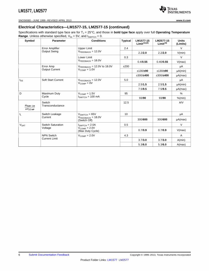
Electrical Characteristics—LM1577-15, LM2577-15Specifications with standard type face are for TJ = 25°C, and those in bold type face apply over full Operating TemperatureRange. Unless otherwise specified, VIN = 5V, and ISWITCH = 0.
Symbol Parameter Conditions Typical LM1577-15 LM2577-15 UnitsLimit (1) (2) Limit (3) (Limits)
SYSTEM PARAMETERS Circuit of Figure 30(4)
VOUT Output Voltage VIN = 5V to 12V 15.0 VILOAD = 100 mA to 600 mA 14.50/14.25 14.50/14.25 V(min)(1)
15.50/15.75 15.50/15.75 V(max)
Line Regulation VIN = 3.5V to 12V 20 mVILOAD = 300 mA mV(max)50/100 50/100
Load Regulation VIN = 5V 20 mVILOAD = 100 mA to 600 mA mV(max)50/100 50/100
η Efficiency VIN = 5V, ILOAD = 600 mA 80 %
DEVICE PARAMETERS
IS Input Supply Current VFEEDBACK = 18.0V 7.5 mA(Switch Off) 10.0/14.0 10.0/14.0 mA(max)
ISWITCH = 2.0A 25 mAVCOMP = 2.0V
50/85 50/85 mA(max)(Max Duty Cycle)
VUV Input Supply ISWITCH = 100 mA 2.90 VUndervoltage 2.70/2.65 2.70/2.65 V(min)Lockout
3.10/3.15 3.10/3.15 V(max)
fO Oscillator Frequency Measured at Switch Pin 52 kHzISWITCH = 100 mA 48/42 48/42 kHz(min)
56/62 56/62 kHz(max)
VREF Output Reference Measured at Feedback Pin VVoltage VIN = 3.5V to 40V 15 14.70/14.55 14.70/14.55 V(min)
VCOMP = 1.0V15.30/15.45 15.30/15.45 V(max)
Output Reference VIN = 3.5V to 40V 10 mVVoltage Line Regulation
RFB Feedback Pin Input 12.2 kΩVoltage Line Regulator
GM Error Amp ICOMP = −30 μA to +30 μA 300 μmhoTransconductance VCOMP = 1.0V 170/110 170/110 μmho(min)
420/500 420/500 μmho(max)
AVOL Error Amp VCOMP = 1.1V to 1.9V 65 V/VVoltage Gain RCOMP = 1.0 MΩ (5)
40/20 40/20 V/V(min)
(1) All limits ensured at room temperature (standard type face) and at temperature extremes (boldface type). All limits are used to calculateOutgoing Quality Level, and are 100% production tested.
(2) A military RETS electrical test specification is available on request. At the time of printing, the LM1577K-12/883, LM1577K-15/883, andLM1577K-ADJ/883 RETS specifications complied fully with the boldface limits in these columns. The LM1577K-12/883, LM1577K-15/883, and LM1577K-ADJ/883 may also be procured to Standard Military Drawing specifications.
(3) All limits ensured at room temperature (standard type face) and at temperature extremes (boldface type). All room temperature limits are100% production tested. All limits at temperature extremes are ensured via correlation using standard Statistical Quality Control (SQC)methods.
(4) External components such as the diode, inductor, input and output capacitors can affect switching regulator performance. When theLM1577/LM2577 is used as shown in the Test Circuit, system performance will be as specified by the system parameters.
(5) A 1.0 MΩ resistor is connected to the compensation pin (which is the error amplifier's output) to ensure accuracy in measuring AVOL. Inactual applications, this pin's load resistance should be ≥10 MΩ, resulting in AVOL that is typically twice the ensured minimum limit.
Copyright © 1999–2013, Texas Instruments Incorporated Submit Documentation Feedback 5
Product Folder Links: LM1577 LM2577
LM1577, LM2577
SNOS658D –JUNE 1999–REVISED APRIL 2013 www.ti.com
Electrical Characteristics—LM1577-15, LM2577-15 (continued)Specifications with standard type face are for TJ = 25°C, and those in bold type face apply over full Operating TemperatureRange. Unless otherwise specified, VIN = 5V, and ISWITCH = 0.
Symbol Parameter Conditions Typical LM1577-15 LM2577-15 UnitsLimit (1) (2) Limit (3) (Limits)
Error Amplifier Upper Limit 2.4 VOutput Swing VFEEDBACK = 12.0V 2.2/2.0 2.2/2.0 V(min)
Lower Limit 0.3 VVFEEDBACK = 18.0V 0.4/0.55 0.40/0.55 V(max)
Error Amp VFEEDBACK = 12.0V to 18.0V ±200 μAOutput Current VCOMP = 1.0V ±130/±90 ±130/±90 μA(min)
±300/±400 ±300/±400 μA(max)
ISS Soft Start Current VFEEDBACK = 12.0V 5.0 μAVCOMP = 0V 2.5/1.5 2.5/1.5 μA(min)
7.5/9.5 7.5/9.5 μA(max)
D Maximum Duty VCOMP = 1.5V 95 %Cycle ISWITCH = 100 mA 93/90 93/90 %(min)
Switch 12.5 A/VTransconductance
IL Switch Leakage VSWITCH = 65V 10 μACurrent VFEEDBACK = 18.0V
300/600 300/600 μA(max)(Switch Off)
VSAT Switch Saturation ISWITCH = 2.0A 0.5 VVoltage VCOMP = 2.0V
0.7/0.9 0.7/0.9 V(max)(Max Duty Cycle)
NPN Switch VCOMP = 2.0V 4.3 ACurrent Limit 3.7/3.0 3.7/3.0 A(min)
5.3/6.0 5.3/6.0 A(max)
6 Submit Documentation Feedback Copyright © 1999–2013, Texas Instruments Incorporated
Product Folder Links: LM1577 LM2577

LM1577, LM2577
www.ti.com SNOS658D –JUNE 1999–REVISED APRIL 2013
Electrical Characteristics—LM1577-ADJ, LM2577-ADJSpecifications with standard type face are for TJ = 25°C, and those in bold type face apply over full Operating TemperatureRange. Unless otherwise specified, VIN = 5V, VFEEDBACK = VREF, and ISWITCH = 0.
Symbol Parameter Conditions Typical LM1577-ADJ LM2577-ADJ UnitsLimit (1) (2) Limit (3) (Limits)
SYSTEM PARAMETERS Circuit of Figure 31 (4)
VOUT Output Voltage VIN = 5V to 10V 12.0 VILOAD = 100 mA to 800 mA (1)
11.60/11.40 11.60/11.40 V(min)
12.40/12.60 12.40/12.60 V(max)
ΔVOUT/ΔVIN Line Regulation VIN = 3.5V to 10V 20 mVILOAD = 300 mA 50/100 50/100 mV(max)
ΔVOUT/ΔILOA Load Regulation VIN = 5V 20 mVD ILOAD = 100 mA to 800 mA 50/100 50/100 mV(max)
η Efficiency VIN = 5V, ILOAD = 800 mA 80 %
DEVICE PARAMETERS
IS Input Supply Current VFEEDBACK = 1.5V (Switch Off) 7.5 mA
10.0/14.0 10.0/14.0 mA(max)
ISWITCH = 2.0A 25 mAVCOMP = 2.0V (Max Duty Cycle) 50/85 50/85 mA(max)
VUV Input Supply ISWITCH = 100 mA 2.90 VUndervoltage Lockout 2.70/2.65 2.70/2.65 V(min)
3.10/3.15 3.10/3.15 V(max)
fO Oscillator Frequency Measured at Switch Pin 52 kHzISWITCH = 100 mA 48/42 48/42 kHz(min)
56/62 56/62 kHz(max)
VREF Reference Measured at Feedback Pin VVoltage VIN = 3.5V to 40V 1.230 1.214/1.206 1.214/1.206 V(min)
VCOMP = 1.0V1.246/1.254 1.246/1.254 V(max)
ΔVREF/ΔVIN Reference Voltage VIN = 3.5V to 40V 0.5 mVLine Regulation
IB Error Amp VCOMP = 1.0V 100 nAInput Bias Current 300/800 300/800 nA(max)
GM Error Amp ICOMP = −30 μA to +30 μA 3700 μmhoTransconductance VCOMP = 1.0V 2400/1600 2400/1600 μmho(min)
4800/5800 4800/5800 μmho(max)
AVOL Error Amp Voltage Gain VCOMP = 1.1V to 1.9V 800 V/VRCOMP = 1.0 MΩ (5)
500/250 500/250 V/V(min)
Error Amplifier Upper Limit 2.4 VOutput Swing VFEEDBACK = 1.0V 2.2/2.0 2.2/2.0 V(min)
Lower Limit 0.3 VVFEEDBACK = 1.5V 0.40/0.55 0.40/0.55 V(max)
(1) All limits ensured at room temperature (standard type face) and at temperature extremes (boldface type). All limits are used to calculateOutgoing Quality Level, and are 100% production tested.
(2) A military RETS electrical test specification is available on request. At the time of printing, the LM1577K-12/883, LM1577K-15/883, andLM1577K-ADJ/883 RETS specifications complied fully with the boldface limits in these columns. The LM1577K-12/883, LM1577K-15/883, and LM1577K-ADJ/883 may also be procured to Standard Military Drawing specifications.
(3) All limits ensured at room temperature (standard type face) and at temperature extremes (boldface type). All room temperature limits are100% production tested. All limits at temperature extremes are ensured via correlation using standard Statistical Quality Control (SQC)methods.
(4) External components such as the diode, inductor, input and output capacitors can affect switching regulator performance. When theLM1577/LM2577 is used as shown in the Test Circuit, system performance will be as specified by the system parameters.
(5) A 1.0 MΩ resistor is connected to the compensation pin (which is the error amplifier's output) to ensure accuracy in measuring AVOL. Inactual applications, this pin's load resistance should be ≥10 MΩ, resulting in AVOL that is typically twice the ensured minimum limit.
Copyright © 1999–2013, Texas Instruments Incorporated Submit Documentation Feedback 7
Product Folder Links: LM1577 LM2577
LM1577, LM2577
SNOS658D –JUNE 1999–REVISED APRIL 2013 www.ti.com
Electrical Characteristics—LM1577-ADJ, LM2577-ADJ (continued)Specifications with standard type face are for TJ = 25°C, and those in bold type face apply over full Operating TemperatureRange. Unless otherwise specified, VIN = 5V, VFEEDBACK = VREF, and ISWITCH = 0.
Symbol Parameter Conditions Typical LM1577-ADJ LM2577-ADJ UnitsLimit (1) (2) Limit (3) (Limits)
Error Amp VFEEDBACK = 1.0V to 1.5V ±200 μAOutput Current VCOMP = 1.0V ±130/±90 ±130/±90 μA(min)
±300/±400 ±300/±400 μA(max)
ISS Soft Start Current VFEEDBACK = 1.0V 5.0 μAVCOMP = 0V 2.5/1.5 2.5/1.5 μA(min)
7.5/9.5 7.5/9.5 μA(max)
D Maximum Duty Cycle VCOMP = 1.5V 95 %ISWITCH = 100 mA 93/90 93/90 %(min)
ΔISWITCH/ΔVC Switch 12.5 A/VOMP Transconductance
IL Switch Leakage VSWITCH = 65V 10 μACurrent VFEEDBACK = 1.5V (Switch Off) 300/600 300/600 μA(max)
VSAT Switch Saturation ISWITCH = 2.0A 0.5 VVoltage VCOMP = 2.0V (Max Duty Cycle) 0.7/0.9 0.7/0.9 V(max)
NPN Switch VCOMP = 2.0V 4.3 ACurrent Limit 3.7/3.0 3.7/3.0 A(min)
5.3/6.0 5.3/6.0 A(max)
THERMAL PARAMETERS (All Versions)
θJA Thermal Resistance K Package, Junction to Ambient 35θJC K Package, Junction to Case 1.5
θJA T Package, Junction to Ambient 65θJC T Package, Junction to Case 2 °C/WθJA N Package, Junction to Ambient (6) 85
θJA M Package, Junction to Ambient (6) 100
θJA S Package, Junction to Ambient (7) 37
(6) Junction to ambient thermal resistance with approximately 1 square inch of pc board copper surrounding the leads. Additional copperarea will lower thermal resistance further. See thermal model in “Switchers Made Simple” software.
(7) If the DDPAK/TO-263 package is used, the thermal resistance can be reduced by increasing the PC board copper area thermallyconnected to the package. Using 0.5 square inches of copper area, θJA is 50°C/W; with 1 square inch of copper area, θJA is 37°C/W;and with 1.6 or more square inches of copper area, θJA is 32°C/W.
8 Submit Documentation Feedback Copyright © 1999–2013, Texas Instruments Incorporated
Product Folder Links: LM1577 LM2577

LM1577, LM2577
www.ti.com SNOS658D –JUNE 1999–REVISED APRIL 2013
Typical Performance Characteristics
Reference Voltage Reference Voltagevs Temperature vs Temperature
Figure 8. Figure 9.
Reference Voltage Δ Reference Voltagevs Temperature vs Supply Voltage
Figure 10. Figure 11.
Δ Reference Voltage Δ Reference Voltagevs Supply Voltage vs Supply Voltage
Figure 12. Figure 13.
Copyright © 1999–2013, Texas Instruments Incorporated Submit Documentation Feedback 9
Product Folder Links: LM1577 LM2577

LM1577, LM2577
SNOS658D –JUNE 1999–REVISED APRIL 2013 www.ti.com
Typical Performance Characteristics (continued)Error Amp Transconductance Error Amp Transconductance
vs Temperature vs Temperature
Figure 14. Figure 15.
Error Amp VoltageGain
Error Amp Transconductance vsvs Temperature Temperature
Figure 16. Figure 17.
Error Amp Voltage Error Amp VoltageGain Gainvs vs
Temperature Temperature
Figure 18. Figure 19.
10 Submit Documentation Feedback Copyright © 1999–2013, Texas Instruments Incorporated
Product Folder Links: LM1577 LM2577

LM1577, LM2577
www.ti.com SNOS658D –JUNE 1999–REVISED APRIL 2013
Typical Performance Characteristics (continued)Quiescent Current Quiescent Current
vs Temperature vs Switch Current
Figure 20. Figure 21.
Current Limit ResponseTime
Current Limit vsvs Temperature Overdrive
Figure 22. Figure 23.
Switch Saturation Voltage Switch Transconductancevs Switch Current vs Temperature
Figure 24. Figure 25.
Copyright © 1999–2013, Texas Instruments Incorporated Submit Documentation Feedback 11
Product Folder Links: LM1577 LM2577

LM1577, LM2577
SNOS658D –JUNE 1999–REVISED APRIL 2013 www.ti.com
Typical Performance Characteristics (continued)Feedback Pin Bias
Currentvs Oscillator Frequency
Temperature vs Temperature
Figure 26. Figure 27.
Maximum Power Dissipation(DDPAK/TO-263) (1)
Figure 28.
(1) If the DDPAK/TO-263 package is used, the thermal resistance can be reduced by increasing the PC board copper area thermallyconnected to the package. Using 0.5 square inches of copper area, θJA is 50°C/W; with 1 square inch of copper area, θJA is 37°C/W;and with 1.6 or more square inches of copper area, θJA is 32°C/W.
12 Submit Documentation Feedback Copyright © 1999–2013, Texas Instruments Incorporated
Product Folder Links: LM1577 LM2577

LM1577, LM2577
www.ti.com SNOS658D –JUNE 1999–REVISED APRIL 2013
LM1577-12, LM2577-12 TEST CIRCUIT
L = 415-0930 (AIE)D = any manufacturerCOUT = Sprague Type 673D
Electrolytic 680 μF, 20VNote: Pin numbers shown are for TO-220 (T) package
Figure 29. Circuit Used to Specify System Parameters for 12V Versions
LM1577-15, LM2577-15 Test Circuit
L = 415-0930 (AIE)D = any manufacturerCOUT = Sprague Type 673D
Electrolytic 680 μF, 20VNote: Pin numbers shown are for TO-220 (T) package
Figure 30. Circuit Used to Specify System Parameters for 15V Versions
Copyright © 1999–2013, Texas Instruments Incorporated Submit Documentation Feedback 13
Product Folder Links: LM1577 LM2577

LM1577, LM2577
SNOS658D –JUNE 1999–REVISED APRIL 2013 www.ti.com
LM1577-ADJ, LM2577-ADJ Test Circuit
L = 415-0930 (AIE)D = any manufacturerCOUT = Sprague Type 673D
Electrolytic 680 μF, 20VR1 = 48.7k in series with 511Ω (1%)R2 = 5.62k (1%)Note: Pin numbers shown are for TO-220 (T) package
Figure 31. Circuit Used to Specify System Parameters for ADJ Versions
Application Hints
Note: Pin numbers shown are for TO-220 (T) package*Resistors are internal to LM1577/LM2577 for 12V and 15V versions.
Figure 32. LM1577/LM2577 Block Diagram and Boost Regulator Application
14 Submit Documentation Feedback Copyright © 1999–2013, Texas Instruments Incorporated
Product Folder Links: LM1577 LM2577

LM1577, LM2577
www.ti.com SNOS658D –JUNE 1999–REVISED APRIL 2013
STEP-UP (BOOST) REGULATOR
Figure 32 shows the LM1577-ADJ/LM2577-ADJ used as a Step-Up Regulator. This is a switching regulator usedfor producing an output voltage greater than the input supply voltage. The LM1577-12/LM2577-12 and LM1577-15/LM2577-15 can also be used for step-up regulators with 12V or 15V outputs (respectively), by tying thefeedback pin directly to the regulator output.
A basic explanation of how it works is as follows. The LM1577/LM2577 turns its output switch on and off at afrequency of 52 kHz, and this creates energy in the inductor (L). When the NPN switch turns on, the inductorcurrent charges up at a rate of VIN/L, storing current in the inductor. When the switch turns off, the lower end ofthe inductor flies above VIN, discharging its current through diode (D) into the output capacitor (COUT) at a rate of(VOUT − VIN)/L. Thus, energy stored in the inductor during the switch on time is transferred to the output duringthe switch off time. The output voltage is controlled by the amount of energy transferred which, in turn, iscontrolled by modulating the peak inductor current. This is done by feeding back a portion of the output voltageto the error amp, which amplifies the difference between the feedback voltage and a 1.230V reference. The erroramp output voltage is compared to a voltage proportional to the switch current (i.e., inductor current during theswitch on time).
The comparator terminates the switch on time when the two voltages are equal, thereby controlling the peakswitch current to maintain a constant output voltage.
Voltage and current waveforms for this circuit are shown in Figure 33, and formulas for calculating them aregiven in Table 1.
Figure 33. Step-Up Regulator Waveforms
Table 1. Step-Up Regulator Formulas (1)
Duty Cycle D
Average Inductor Current IIND(AVE)
Inductor Current Ripple ΔIIND
Peak Inductor CurrentIIND(PK)
Peak Switch Current ISW(PK)
Switch Voltage When Off VSW(OFF) VOUT + VF
Diode Reverse Voltage VR VOUT − VSAT
Average Diode Current ID(AVE) ILOAD
Peak Diode CurrentID(PK)
Power Dissipation of LM1577/2577PD
(1) VF = Forward Biased Diode VoltageILOAD = Output Load Current
Copyright © 1999–2013, Texas Instruments Incorporated Submit Documentation Feedback 15
Product Folder Links: LM1577 LM2577

LM1577, LM2577
SNOS658D –JUNE 1999–REVISED APRIL 2013 www.ti.com
STEP-UP REGULATOR DESIGN PROCEDURE
The following design procedure can be used to select the appropriate external components for the circuit inFigure 32, based on these system requirements.
Given:• VIN (min) = Minimum input supply voltage• VOUT = Regulated output voltage• ILOAD(max) = Maximum output load current• Before proceeding any further, determine if the LM1577/LM2577 can provide these values of VOUT and
ILOAD(max) when operating with the minimum value of VIN. The upper limits for VOUT and ILOAD(max) are given bythe following equations.
where• VOUT ≤ 60V• VOUT ≤ 10 × VIN(min) (3)
These limits must be greater than or equal to the values specified in this application.
1. Inductor Selection (L)A. Voltage Options:1. For 12V or 15V outputFrom Figure 34 (for 12V output) or Figure 35 (for 15V output), identify inductor code for regionindicated by VIN (min) and ILOAD (max). The shaded region indicates conditions for which the LM1577/LM2577output switch would be operating beyond its switch current rating. The minimum operating voltage for theLM1577/LM2577 is 3.5V.From here, proceed to step C.2. For Adjustable versionPreliminary calculations:The inductor selection is based on the calculation of the following three parameters:D(max), the maximum switch duty cycle (0 ≤ D ≤ 0.9):
(4)
where VF = 0.5V for Schottky diodes and 0.8V for fast recovery diodes (typically);
E •T, the product of volts × time that charges the inductor:
(5)
IIND,DC, the average inductor current under full load;
(6)
B. Identify Inductor Value:1. From Figure 36, identify the inductor code for the region indicated by the intersection of E•T and IIND,DC.This code gives the inductor value in microhenries. The L or H prefix signifies whether the inductor is ratedfor a maximum E•T of 90 V•μs (L) or 250 V•μs (H).2. If D < 0.85, go on to step C. If D ≥ 0.85, then calculate the minimum inductance needed to ensure theswitching regulator's stability:
(7)
If LMIN is smaller than the inductor value found in step B1, go on to step C. Otherwise, the inductor value found instep B1 is too low; an appropriate inductor code should be obtained from the graph as follows:
1. Find the lowest value inductor that is greater than LMIN.
16 Submit Documentation Feedback Copyright © 1999–2013, Texas Instruments Incorporated
Product Folder Links: LM1577 LM2577

LM1577, LM2577
www.ti.com SNOS658D –JUNE 1999–REVISED APRIL 2013
2. Find where E•T intersects this inductor value to determine if it has an L or H prefix. If E•T intersects both the Land H regions, select the inductor with an H prefix.
Figure 34. LM2577-12 Inductor Selection Guide
Figure 35. LM2577-15 Inductor Selection Guide
Copyright © 1999–2013, Texas Instruments Incorporated Submit Documentation Feedback 17
Product Folder Links: LM1577 LM2577

LM1577, LM2577
SNOS658D –JUNE 1999–REVISED APRIL 2013 www.ti.com
Note: These charts assume that the inductor ripple current is approximately 20% to 30% of the average inductorcurrent (when the regulator is under full load). Greater ripple current causes higher peak switch currents and greateroutput ripple voltage; lower ripple current is achieved with larger-value inductors. The factor of 20 to 30% is chosen asa convenient balance between the two extremes.
Figure 36. LM1577-ADJ/LM2577-ADJ Inductor Selection Graph
C. Select an inductor from Table 2 which cross-references the inductor codes to the part numbers of threedifferent manufacturers. Complete specifications for these inductors are available from the respectivemanufacturers. The inductors listed in this table have the following characteristics:• AIE: ferrite, pot-core inductors; Benefits of this type are low electro-magnetic interference (EMI), small
physical size, and very low power dissipation (core loss). Be careful not to operate these inductors toofar beyond their maximum ratings for E•T and peak current, as this will saturate the core.
• Pulse: powdered iron, toroid core inductors; Benefits are low EMI and ability to withstand E•T and peakcurrent above rated value better than ferrite cores.
• Renco: ferrite, bobbin-core inductors; Benefits are low cost and best ability to withstand E•T and peakcurrent above rated value. Be aware that these inductors generate more EMI than the other types, andthis may interfere with signals sensitive to noise.
18 Submit Documentation Feedback Copyright © 1999–2013, Texas Instruments Incorporated
Product Folder Links: LM1577 LM2577

LM1577, LM2577
www.ti.com SNOS658D –JUNE 1999–REVISED APRIL 2013
Table 2. Table of Standardized Inductors andManufacturer's Part Numbers (1)
Inductor Manufacturer's Part Number
Code Schott Pulse Renco
L47 67126980 PE - 53112 RL2442
L68 67126990 PE - 92114 RL2443
L100 67127000 PE - 92108 RL2444
L150 67127010 PE - 53113 RL1954
L220 67127020 PE - 52626 RL1953
L330 67127030 PE - 52627 RL1952
L470 67127040 PE - 53114 RL1951
L680 67127050 PE - 52629 RL1950
H150 67127060 PE - 53115 RL2445
H220 67127070 PE - 53116 RL2446
H330 67127080 PE - 53117 RL2447
H470 67127090 PE - 53118 RL1961
H680 67127100 PE - 53119 RL1960
H1000 67127110 PE - 53120 RL1959
H1500 67127120 PE - 53121 RL1958
H2200 67127130 PE - 53122 RL2448
(1) Schott Corp., (612) 475-11731000 Parkers Lake Rd., Wayzata, MN 55391Pulse Engineering, (619) 268-2400P.O. Box 12235, San Diego, CA 92112Renco Electronics Inc., (516) 586-556660 Jeffryn Blvd. East, Deer Park, NY 11729
2. Compensation Network (RC, CC) and Output Capacitor (COUT) Selection
RC and CC form a pole-zero compensation network that stabilizes the regulator. The values of RC and CC aremainly dependant on the regulator voltage gain, ILOAD(max), L and COUT. The following procedure calculates valuesfor RC, CC, and COUT that ensure regulator stability. Be aware that this procedure doesn't necessarily result in RCand CC that provide optimum compensation. In order to ensure optimum compensation, one of the standardprocedures for testing loop stability must be used, such as measuring VOUT transient response when pulsingILOAD (see Figure 39).
A. First, calculate the maximum value for RC.
(8)
Select a resistor less than or equal to this value, and it should also be no greater than 3 kΩ.
B. Calculate the minimum value for COUT using the following two equations.
(9)
The larger of these two values is the minimum value that ensures stability.
C. Calculate the minimum value of CC .
(10)
Copyright © 1999–2013, Texas Instruments Incorporated Submit Documentation Feedback 19
Product Folder Links: LM1577 LM2577
LM1577, LM2577
SNOS658D –JUNE 1999–REVISED APRIL 2013 www.ti.com
The compensation capacitor is also part of the soft start circuitry. When power to the regulator is turned on, theswitch duty cycle is allowed to rise at a rate controlled by this capacitor (with no control on the duty cycle, itwould immediately rise to 90%, drawing huge currents from the input power supply). In order to operate properly,the soft start circuit requires CC ≥ 0.22 μF.
The value of the output filter capacitor is normally large enough to require the use of aluminum electrolyticcapacitors. Table 3 lists several different types that are recommended for switching regulators, and the followingparameters are used to select the proper capacitor.
Working Voltage (WVDC): Choose a capacitor with a working voltage at least 20% higher than the regulatoroutput voltage.
Ripple Current: This is the maximum RMS value of current that charges the capacitor during each switchingcycle. For step-up and flyback regulators, the formula for ripple current is
(11)
Choose a capacitor that is rated at least 50% higher than this value at 52 kHz.
Equivalent Series Resistance (ESR) : This is the primary cause of output ripple voltage, and it also affects thevalues of RC and CC needed to stabilize the regulator. As a result, the preceding calculations for CC and RC areonly valid if ESR doesn't exceed the maximum value specified by the following equations.
(12)
Select a capacitor with ESR, at 52 kHz, that is less than or equal to the lower value calculated. Most electrolyticcapacitors specify ESR at 120 Hz which is 15% to 30% higher than at 52 kHz. Also, be aware that ESRincreases by a factor of 2 when operating at −20°C.
In general, low values of ESR are achieved by using large value capacitors (C ≥ 470 μF), and capacitors withhigh WVDC, or by paralleling smaller-value capacitors.
3. Output Voltage Selection (R1 and R2)
This section is for applications using the LM1577-ADJ/LM2577-ADJ. Skip this section if the LM1577-12/LM2577-12 or LM1577-15/LM2577-15 is being used.
With the LM1577-ADJ/LM2577-ADJ, the output voltage is given byVOUT = 1.23V (1 + R1/R2) (13)
Resistors R1 and R2 divide the output down so it can be compared with the LM1577-ADJ/LM2577-ADJ internal1.23V reference. For a given desired output voltage VOUT, select R1 and R2 so that
(14)
4. Input Capacitor Selection (CIN)
The switching action in the step-up regulator causes a triangular ripple current to be drawn from the supplysource. This in turn causes noise to appear on the supply voltage. For proper operation of the LM1577, the inputvoltage should be decoupled. Bypassing the Input Voltage pin directly to ground with a good quality, low ESR,0.1 μF capacitor (leads as short as possible) is normally sufficient.
20 Submit Documentation Feedback Copyright © 1999–2013, Texas Instruments Incorporated
Product Folder Links: LM1577 LM2577
LM1577, LM2577
www.ti.com SNOS658D –JUNE 1999–REVISED APRIL 2013
Table 3. Aluminum Electrolytic CapacitorsRecommended for Switching Regulators
Cornell Dublier —Types 239, 250, 251, UFT, 300, or 350
P.O. Box 128, Pickens, SC 29671(803) 878-6311
Nichicon —Types PF, PX, or PZ
927 East Parkway,Schaumburg, IL 60173(708) 843-7500
Sprague —Types 672D, 673D, or 674D
Box 1, Sprague Road,Lansing, NC 28643(919) 384-2551
United Chemi-Con —Types LX, SXF, or SXJ
9801 West Higgins Road,Rosemont, IL 60018(708) 696-2000
If the LM1577 is located far from the supply source filter capacitors, an additional large electrolytic capacitor (e.g.47 μF) is often required.
5. Diode Selection (D)
The switching diode used in the boost regulator must withstand a reverse voltage equal to the circuit outputvoltage, and must conduct the peak output current of the LM2577. A suitable diode must have a minimumreverse breakdown voltage greater than the circuit output voltage, and should be rated for average and peakcurrent greater than ILOAD(max) and ID(PK). Schottky barrier diodes are often favored for use in switching regulators.Their low forward voltage drop allows higher regulator efficiency than if a (less expensive) fast recovery diodewas used. See Table 4 for recommended part numbers and voltage ratings of 1A and 3A diodes.
Table 4. Diode Selection Chart
VOUT Schottky Fast Recovery
(max) 1A 3A 1A 3A
20V 1N5817 1N5820
MBR120P MBR320P
1N5818 1N5821
30V MBR130P MBR330P
11DQ03 31DQ03
1N5819 1N5822
40V MBR140P MBR340P
11DQ04 31DQ04
MBR150 MBR350 1N4933
50V 11DQ05 31DQ05 MUR105
1N4934 MR851
100V HER102 30DL1
MUR110 MR831
10DL1 HER302
BOOST REGULATOR CIRCUIT EXAMPLE
By adding a few external components (as shown in Figure 37), the LM2577 can be used to produce a regulatedoutput voltage that is greater than the applied input voltage. Typical performance of this regulator is shown inFigure 38 and Figure 39. The switching waveforms observed during the operation of this circuit are shown inFigure 40.
Copyright © 1999–2013, Texas Instruments Incorporated Submit Documentation Feedback 21
Product Folder Links: LM1577 LM2577

LM1577, LM2577
SNOS658D –JUNE 1999–REVISED APRIL 2013 www.ti.com
Note: Pin numbers shown are for TO-220 (T) package.
Figure 37. Step-up Regulator Delivers 12V from a 5V Input
Figure 38. Line Regulation (Typical) of Step-Up Regulator of Figure 37
A: Output Voltage Change, 100 mV/div. (AC-coupled)B: Load current, 0.2 A/divHorizontal: 5 ms/div
Figure 39. Load Transient Response of Step-UpRegulator of Figure 37
22 Submit Documentation Feedback Copyright © 1999–2013, Texas Instruments Incorporated
Product Folder Links: LM1577 LM2577

LM1577, LM2577
www.ti.com SNOS658D –JUNE 1999–REVISED APRIL 2013
A: Switch pin voltage, 10 V/divB: Switch pin current, 2 A/divC: Inductor current, 2 A/divD: Output ripple voltage, 100 mV/div (AC-coupled)Horizontal: 5 μs/div
Figure 40. Switching Waveforms of Step-UpRegulator of Figure 37
FLYBACK REGULATOR
A Flyback regulator can produce single or multiple output voltages that are lower or greater than the input supplyvoltage. Figure 42 shows the LM1577/LM2577 used as a flyback regulator with positive and negative regulatedoutputs. Its operation is similar to a step-up regulator, except the output switch contols the primary current of aflyback transformer. Note that the primary and secondary windings are out of phase, so no current flows throughsecondary when current flows through the primary. This allows the primary to charge up the transformer corewhen the switch is on. When the switch turns off, the core discharges by sending current through the secondary,and this produces voltage at the outputs. The output voltages are controlled by adjusting the peak primarycurrent, as described in the STEP-UP (BOOST) REGULATOR section.
Voltage and current waveforms for this circuit are shown in Figure 41, and formulas for calculating them aregiven in Table 5.
FLYBACK REGULATOR DESIGN PROCEDURE
1. Transformer Selection
A family of standardized flyback transformers is available for creating flyback regulators that produce dual outputvoltages, from ±10V to ±15V, as shown in Figure 42. Table 6 lists these transformers with the input voltage,output voltages and maximum load current they are designed for.
2. Compensation Network (CC, RC) andOutput Capacitor (COUT) Selection
As explained in the Step-Up Regulator Design Procedure, CC, RC and COUT must be selected as a group. Thefollowing procedure is for a dual output flyback regulator with equal turns ratios for each secondary (i.e., bothoutput voltages have the same magnitude). The equations can be used for a single output regulator by changing∑ILOAD(max) to ILOAD(max) in the following equations.
A. First, calculate the maximum value for RC.
Copyright © 1999–2013, Texas Instruments Incorporated Submit Documentation Feedback 23
Product Folder Links: LM1577 LM2577

LM1577, LM2577
SNOS658D –JUNE 1999–REVISED APRIL 2013 www.ti.com
(15)
Where ∑ILOAD(max) is the sum of the load current (magnitude) required from both outputs. Select a resistor lessthan or equal to this value, and no greater than 3 kΩ.
B. Calculate the minimum value for ∑COUT (sum of COUT at both outputs) using the following two equations.
(16)
The larger of these two values must be used to ensure regulator stability.
Figure 41. Flyback Regulator Waveforms
T1 = Pulse Engineering, PE-65300D1, D2 = 1N5821
Figure 42. LM1577-ADJ/LM2577-ADJ Flyback Regulator with ± Outputs
Table 5. Flyback Regulator Formulas
Duty Cycle D
(17)
Primary Current VariationΔIP
(18)
24 Submit Documentation Feedback Copyright © 1999–2013, Texas Instruments Incorporated
Product Folder Links: LM1577 LM2577

LM1577, LM2577
www.ti.com SNOS658D –JUNE 1999–REVISED APRIL 2013
Table 5. Flyback Regulator Formulas (continued)
Peak Primary CurrentIP(PK)
(19)
Switch Voltage when OffVSW(OFF)
(20)
Diode Reverse Voltage VR VOUT+ N (VIN
− VSAT)
Average Diode Current ID(AVE) ILOAD
Peak Diode CurrentID(PK)
(21)
Short Circuit Diode Current
(22)
Power Dissipation of LM1577/LM2577
PD
(23)
C. Calculate the minimum value of CC
(24)
D. Calculate the maximum ESR of the +VOUT and −VOUT output capacitors in parallel.
(25)
This formula can also be used to calculate the maximum ESR of a single output regulator.
At this point, refer to this same section in the STEP-UP REGULATOR DESIGN PROCEDURE section for moreinformation regarding the selection of COUT.
3. Output Voltage Selection
This section is for applications using the LM1577-ADJ/LM2577-ADJ. Skip this section if the LM1577-12/LM2577-12 or LM1577-15/LM2577-15 is being used.
With the LM1577-ADJ/LM2577-ADJ, the output voltage is given byVOUT = 1.23V (1 + R1/R2) (26)
Resistors R1 and R2 divide the output voltage down so it can be compared with the LM1577-ADJ/LM2577-ADJinternal 1.23V reference. For a desired output voltage VOUT, select R1 and R2 so that
(27)
4. Diode Selection
The switching diode in a flyback converter must withstand the reverse voltage specified by the followingequation.
(28)
A suitable diode must have a reverse voltage rating greater than this. In addition it must be rated for more thanthe average and peak diode currents listed in Table 5.
5. Input Capacitor Selection
Copyright © 1999–2013, Texas Instruments Incorporated Submit Documentation Feedback 25
Product Folder Links: LM1577 LM2577

LM1577, LM2577
SNOS658D –JUNE 1999–REVISED APRIL 2013 www.ti.com
The primary of a flyback transformer draws discontinuous pulses of current from the input supply. As a result, aflyback regulator generates more noise at the input supply than a step-up regulator, and this requires a largerbypass capacitor to decouple the LM1577/LM2577 VIN pin from this noise. For most applications, a low ESR, 1.0μF cap will be sufficient, if it is connected very close to the VIN and Ground pins.
Transformer Input Dual Maximum
Type Voltage Output Output
Voltage Current
LP = 100 μH 5V ±10V 325 mA
1 N = 1 5V ±12V 275 mA
5V ±15V 225 mA
10V ±10V 700 mA
10V ±12V 575 mA
2 LP = 200 μH 10V ±15V 500 mA
N = 0.5 12V ±10V 800 mA
12V ±12V 700 mA
12V ±15V 575 mA
3 LP = 250 μH 15V ±10V 900 mA
N = 0.5 15V ±12V 825 mA
15V ±15V 700 mA
Table 6. Flyback Transformer Selection Guide
Transformer Manufacturers' Part Numbers
Type AIE Pulse Renco
1 326-0637 PE-65300 RL-2580
2 330-0202 PE-65301 RL-2581
3 330-0203 PE-65302 RL-2582
In addition to this bypass cap, a larger capacitor (≥ 47 μF) should be used where the flyback transformerconnects to the input supply. This will attenuate noise which may interfere with other circuits connected to thesame input supply voltage.
6. Snubber Circuit
A “snubber” circuit is required when operating from input voltages greater than 10V, or when using a transformerwith LP ≥ 200 μH. This circuit clamps a voltage spike from the transformer primary that occurs immediately afterthe output switch turns off. Without it, the switch voltage may exceed the 65V maximum rating. As shown inFigure 43, the snubber consists of a fast recovery diode, and a parallel RC. The RC values are selected forswitch clamp voltage (VCLAMP) that is 5V to 10V greater than VSW(OFF). Use the following equations to calculate Rand C;
(29)
Power dissipation (and power rating) of the resistor is;
(30)
The fast recovery diode must have a reverse voltage rating greater than VCLAMP.
26 Submit Documentation Feedback Copyright © 1999–2013, Texas Instruments Incorporated
Product Folder Links: LM1577 LM2577

LM1577, LM2577
www.ti.com SNOS658D –JUNE 1999–REVISED APRIL 2013
Figure 43. Snubber Circuit
FLYBACK REGULATOR CIRCUIT EXAMPLE
The circuit of Figure 44 produces ±15V (at 225 mA each) from a single 5V input. The output regulation of thiscircuit is shown in Figure 45 and Figure 47, while the load transient response is shown in Figure 46 andFigure 48. Switching waveforms seen in this circuit are shown in Figure 49.
T1 = Pulse Engineering, PE-65300D1, D2 = 1N5821
Figure 44. Flyback Regulator Easily Provides Dual Outputs
Figure 45. Line Regulation (Typical) of FlybackRegulator of Figure 44, +15V Output
Copyright © 1999–2013, Texas Instruments Incorporated Submit Documentation Feedback 27
Product Folder Links: LM1577 LM2577

LM1577, LM2577
SNOS658D –JUNE 1999–REVISED APRIL 2013 www.ti.com
A: Output Voltage Change, 100 mV/divB: Output Current, 100 mA/divHorizontal: 10 ms/div
Figure 46. Load Transient Response of FlybackRegulator of Figure 44, +15V Output
Figure 47. Line Regulation (Typical) of FlybackRegulator of Figure 44, −15V Output
28 Submit Documentation Feedback Copyright © 1999–2013, Texas Instruments Incorporated
Product Folder Links: LM1577 LM2577

LM1577, LM2577
www.ti.com SNOS658D –JUNE 1999–REVISED APRIL 2013
A: Output Voltage Change, 100 mV/divB: Output Current, 100 mA/divHorizontal: 10 ms/div
Figure 48. Load Transient Response of FlybackRegulator of Figure 44, −15V Output
A: Switch pin voltage, 20 V/divB: Primary current, 2 A/divC: +15V Secondary current, 1 A/divD: +15V Output ripple voltage, 100 mV/divHorizontal: 5 μs/div
Figure 49. Switching Waveforms of Flyback Regulator of Figure 44, Each Output Loaded with 60Ω
Copyright © 1999–2013, Texas Instruments Incorporated Submit Documentation Feedback 29
Product Folder Links: LM1577 LM2577

LM1577, LM2577
SNOS658D –JUNE 1999–REVISED APRIL 2013 www.ti.com
REVISION HISTORY
Changes from Revision C (April 2013) to Revision D Page
• Changed layout of National Data Sheet to TI format .......................................................................................................... 29
30 Submit Documentation Feedback Copyright © 1999–2013, Texas Instruments Incorporated
Product Folder Links: LM1577 LM2577

PACKAGE OPTION ADDENDUM
www.ti.com 17-Mar-2017
Addendum-Page 1
PACKAGING INFORMATION
Orderable Device Status(1)
Package Type PackageDrawing
Pins PackageQty
Eco Plan(2)
Lead/Ball Finish(6)
MSL Peak Temp(3)
Op Temp (°C) Device Marking(4/5)
Samples
LM2577S-ADJ NRND DDPAK/TO-263
KTT 5 45 TBD Call TI Call TI -40 to 125 LM2577S-ADJ P+
LM2577S-ADJ/NOPB ACTIVE DDPAK/TO-263
KTT 5 45 Pb-Free (RoHSExempt)
CU SN Level-3-245C-168 HR -40 to 125 LM2577S-ADJ P+
LM2577SX-ADJ NRND DDPAK/TO-263
KTT 5 500 TBD Call TI Call TI -40 to 125 LM2577S-ADJ P+
LM2577SX-ADJ/NOPB ACTIVE DDPAK/TO-263
KTT 5 500 Pb-Free (RoHSExempt)
CU SN Level-3-245C-168 HR -40 to 125 LM2577S-ADJ P+
LM2577T-ADJ NRND TO-220 KC 5 45 TBD Call TI Call TI -40 to 125 LM2577T-ADJP+
LM2577T-ADJ/LB03 NRND TO-220 NDH 5 45 TBD Call TI Call TI LM2577T-ADJP+
LM2577T-ADJ/LF03 ACTIVE TO-220 NDH 5 45 Green (RoHS& no Sb/Br)
CU SN Level-1-NA-UNLIM LM2577T-ADJP+
LM2577T-ADJ/NOPB ACTIVE TO-220 KC 5 45 Pb-Free (RoHSExempt)
CU SN Level-1-NA-UNLIM -40 to 125 LM2577T-ADJP+
(1) The marketing status values are defined as follows:ACTIVE: Product device recommended for new designs.LIFEBUY: TI has announced that the device will be discontinued, and a lifetime-buy period is in effect.NRND: Not recommended for new designs. Device is in production to support existing customers, but TI does not recommend using this part in a new design.PREVIEW: Device has been announced but is not in production. Samples may or may not be available.OBSOLETE: TI has discontinued the production of the device.
(2) Eco Plan - The planned eco-friendly classification: Pb-Free (RoHS), Pb-Free (RoHS Exempt), or Green (RoHS & no Sb/Br) - please check http://www.ti.com/productcontent for the latest availabilityinformation and additional product content details.TBD: The Pb-Free/Green conversion plan has not been defined.Pb-Free (RoHS): TI's terms "Lead-Free" or "Pb-Free" mean semiconductor products that are compatible with the current RoHS requirements for all 6 substances, including the requirement thatlead not exceed 0.1% by weight in homogeneous materials. Where designed to be soldered at high temperatures, TI Pb-Free products are suitable for use in specified lead-free processes.Pb-Free (RoHS Exempt): This component has a RoHS exemption for either 1) lead-based flip-chip solder bumps used between the die and package, or 2) lead-based die adhesive used betweenthe die and leadframe. The component is otherwise considered Pb-Free (RoHS compatible) as defined above.Green (RoHS & no Sb/Br): TI defines "Green" to mean Pb-Free (RoHS compatible), and free of Bromine (Br) and Antimony (Sb) based flame retardants (Br or Sb do not exceed 0.1% by weightin homogeneous material)

PACKAGE OPTION ADDENDUM
www.ti.com 17-Mar-2017
Addendum-Page 2
(3) MSL, Peak Temp. - The Moisture Sensitivity Level rating according to the JEDEC industry standard classifications, and peak solder temperature.
(4) There may be additional marking, which relates to the logo, the lot trace code information, or the environmental category on the device.
(5) Multiple Device Markings will be inside parentheses. Only one Device Marking contained in parentheses and separated by a "~" will appear on a device. If a line is indented then it is a continuationof the previous line and the two combined represent the entire Device Marking for that device.
(6) Lead/Ball Finish - Orderable Devices may have multiple material finish options. Finish options are separated by a vertical ruled line. Lead/Ball Finish values may wrap to two lines if the finishvalue exceeds the maximum column width.
Important Information and Disclaimer:The information provided on this page represents TI's knowledge and belief as of the date that it is provided. TI bases its knowledge and belief on informationprovided by third parties, and makes no representation or warranty as to the accuracy of such information. Efforts are underway to better integrate information from third parties. TI has taken andcontinues to take reasonable steps to provide representative and accurate information but may not have conducted destructive testing or chemical analysis on incoming materials and chemicals.TI and TI suppliers consider certain information to be proprietary, and thus CAS numbers and other limited information may not be available for release.
In no event shall TI's liability arising out of such information exceed the total purchase price of the TI part(s) at issue in this document sold by TI to Customer on an annual basis.

TAPE AND REEL INFORMATION
*All dimensions are nominal
Device PackageType
PackageDrawing
Pins SPQ ReelDiameter
(mm)
ReelWidth
W1 (mm)
A0(mm)
B0(mm)
K0(mm)
P1(mm)
W(mm)
Pin1Quadrant
LM2577SX-ADJ DDPAK/TO-263
KTT 5 500 330.0 24.4 10.75 14.85 5.0 16.0 24.0 Q2
LM2577SX-ADJ/NOPB DDPAK/TO-263
KTT 5 500 330.0 24.4 10.75 14.85 5.0 16.0 24.0 Q2
PACKAGE MATERIALS INFORMATION
www.ti.com 1-Oct-2016
Pack Materials-Page 1

*All dimensions are nominal
Device Package Type Package Drawing Pins SPQ Length (mm) Width (mm) Height (mm)
LM2577SX-ADJ DDPAK/TO-263 KTT 5 500 367.0 367.0 45.0
LM2577SX-ADJ/NOPB DDPAK/TO-263 KTT 5 500 367.0 367.0 45.0
PACKAGE MATERIALS INFORMATION
www.ti.com 1-Oct-2016
Pack Materials-Page 2

www.ti.com
PACKAGE OUTLINE
C
B
9.257.67
6.865.69
3.052.54
14.7312.29
5X 1.020.64
4X 1.7
8.896.86
12.8810.08
(6.275)
4.834.06
1.401.14
3.052.03
0.610.30
-3.963.71
6.8
2X (R1)OPTIONAL
16.51MAX
A10.679.65
(4.25)
4215009/A 01/2017
TO-220 - 16.51 mm max heightKC0005ATO-220
NOTES: 1. All controlling linear dimensions are in inches. Dimensions in brackets are in millimeters. Any dimension in brackets or parenthesis are for reference only. Dimensioning and tolerancing per ASME Y14.5M.2. This drawing is subject to change without notice.3. Shape may vary per different assembly sites.
0.25 C A B
PIN 1 ID(OPTIONAL)
1 5
OPTIONALCHAMFER
SCALE 0.850
NOTE 3
1 5
AAAA

www.ti.com
EXAMPLE BOARD LAYOUT
0.07 MAXALL AROUND
0.07 MAXALL AROUND (1.45)
(2)
(R0.05) TYP
4X (1.45)
4X (2)
5X ( 1.2)(1.7) TYP
(6.8)
FULL RTYP
TO-220 - 16.51 mm max heightKC0005ATO-220
4215009/A 01/2017
LAND PATTERNNON-SOLDER MASK DEFINED
SCALE:12X
PKG
PKG
METALTYP
SOLDER MASKOPENING, TYP
1 5

MECHANICAL DATA
NDH0005D
www.ti.com

MECHANICAL DATA
KTT0005B
www.ti.com
BOTTOM SIDE OF PACKAGE
TS5B (Rev D)

MECHANICAL DATA
NEB0005B
www.ti.com

IMPORTANT NOTICE
Texas Instruments Incorporated (TI) reserves the right to make corrections, enhancements, improvements and other changes to itssemiconductor products and services per JESD46, latest issue, and to discontinue any product or service per JESD48, latest issue. Buyersshould obtain the latest relevant information before placing orders and should verify that such information is current and complete.TI’s published terms of sale for semiconductor products (http://www.ti.com/sc/docs/stdterms.htm) apply to the sale of packaged integratedcircuit products that TI has qualified and released to market. Additional terms may apply to the use or sale of other types of TI products andservices.Reproduction of significant portions of TI information in TI data sheets is permissible only if reproduction is without alteration and isaccompanied by all associated warranties, conditions, limitations, and notices. TI is not responsible or liable for such reproduceddocumentation. Information of third parties may be subject to additional restrictions. Resale of TI products or services with statementsdifferent from or beyond the parameters stated by TI for that product or service voids all express and any implied warranties for theassociated TI product or service and is an unfair and deceptive business practice. TI is not responsible or liable for any such statements.Buyers and others who are developing systems that incorporate TI products (collectively, “Designers”) understand and agree that Designersremain responsible for using their independent analysis, evaluation and judgment in designing their applications and that Designers havefull and exclusive responsibility to assure the safety of Designers' applications and compliance of their applications (and of all TI productsused in or for Designers’ applications) with all applicable regulations, laws and other applicable requirements. Designer represents that, withrespect to their applications, Designer has all the necessary expertise to create and implement safeguards that (1) anticipate dangerousconsequences of failures, (2) monitor failures and their consequences, and (3) lessen the likelihood of failures that might cause harm andtake appropriate actions. Designer agrees that prior to using or distributing any applications that include TI products, Designer willthoroughly test such applications and the functionality of such TI products as used in such applications.TI’s provision of technical, application or other design advice, quality characterization, reliability data or other services or information,including, but not limited to, reference designs and materials relating to evaluation modules, (collectively, “TI Resources”) are intended toassist designers who are developing applications that incorporate TI products; by downloading, accessing or using TI Resources in anyway, Designer (individually or, if Designer is acting on behalf of a company, Designer’s company) agrees to use any particular TI Resourcesolely for this purpose and subject to the terms of this Notice.TI’s provision of TI Resources does not expand or otherwise alter TI’s applicable published warranties or warranty disclaimers for TIproducts, and no additional obligations or liabilities arise from TI providing such TI Resources. TI reserves the right to make corrections,enhancements, improvements and other changes to its TI Resources. TI has not conducted any testing other than that specificallydescribed in the published documentation for a particular TI Resource.Designer is authorized to use, copy and modify any individual TI Resource only in connection with the development of applications thatinclude the TI product(s) identified in such TI Resource. NO OTHER LICENSE, EXPRESS OR IMPLIED, BY ESTOPPEL OR OTHERWISETO ANY OTHER TI INTELLECTUAL PROPERTY RIGHT, AND NO LICENSE TO ANY TECHNOLOGY OR INTELLECTUAL PROPERTYRIGHT OF TI OR ANY THIRD PARTY IS GRANTED HEREIN, including but not limited to any patent right, copyright, mask work right, orother intellectual property right relating to any combination, machine, or process in which TI products or services are used. Informationregarding or referencing third-party products or services does not constitute a license to use such products or services, or a warranty orendorsement thereof. Use of TI Resources may require a license from a third party under the patents or other intellectual property of thethird party, or a license from TI under the patents or other intellectual property of TI.TI RESOURCES ARE PROVIDED “AS IS” AND WITH ALL FAULTS. TI DISCLAIMS ALL OTHER WARRANTIES ORREPRESENTATIONS, EXPRESS OR IMPLIED, REGARDING RESOURCES OR USE THEREOF, INCLUDING BUT NOT LIMITED TOACCURACY OR COMPLETENESS, TITLE, ANY EPIDEMIC FAILURE WARRANTY AND ANY IMPLIED WARRANTIES OFMERCHANTABILITY, FITNESS FOR A PARTICULAR PURPOSE, AND NON-INFRINGEMENT OF ANY THIRD PARTY INTELLECTUALPROPERTY RIGHTS. TI SHALL NOT BE LIABLE FOR AND SHALL NOT DEFEND OR INDEMNIFY DESIGNER AGAINST ANY CLAIM,INCLUDING BUT NOT LIMITED TO ANY INFRINGEMENT CLAIM THAT RELATES TO OR IS BASED ON ANY COMBINATION OFPRODUCTS EVEN IF DESCRIBED IN TI RESOURCES OR OTHERWISE. IN NO EVENT SHALL TI BE LIABLE FOR ANY ACTUAL,DIRECT, SPECIAL, COLLATERAL, INDIRECT, PUNITIVE, INCIDENTAL, CONSEQUENTIAL OR EXEMPLARY DAMAGES INCONNECTION WITH OR ARISING OUT OF TI RESOURCES OR USE THEREOF, AND REGARDLESS OF WHETHER TI HAS BEENADVISED OF THE POSSIBILITY OF SUCH DAMAGES.Unless TI has explicitly designated an individual product as meeting the requirements of a particular industry standard (e.g., ISO/TS 16949and ISO 26262), TI is not responsible for any failure to meet such industry standard requirements.Where TI specifically promotes products as facilitating functional safety or as compliant with industry functional safety standards, suchproducts are intended to help enable customers to design and create their own applications that meet applicable functional safety standardsand requirements. Using products in an application does not by itself establish any safety features in the application. Designers mustensure compliance with safety-related requirements and standards applicable to their applications. Designer may not use any TI products inlife-critical medical equipment unless authorized officers of the parties have executed a special contract specifically governing such use.Life-critical medical equipment is medical equipment where failure of such equipment would cause serious bodily injury or death (e.g., lifesupport, pacemakers, defibrillators, heart pumps, neurostimulators, and implantables). Such equipment includes, without limitation, allmedical devices identified by the U.S. Food and Drug Administration as Class III devices and equivalent classifications outside the U.S.TI may expressly designate certain products as completing a particular qualification (e.g., Q100, Military Grade, or Enhanced Product).Designers agree that it has the necessary expertise to select the product with the appropriate qualification designation for their applicationsand that proper product selection is at Designers’ own risk. Designers are solely responsible for compliance with all legal and regulatoryrequirements in connection with such selection.Designer will fully indemnify TI and its representatives against any damages, costs, losses, and/or liabilities arising out of Designer’s non-compliance with the terms and provisions of this Notice.
Mailing Address: Texas Instruments, Post Office Box 655303, Dallas, Texas 75265Copyright © 2017, Texas Instruments Incorporated