lm231a/lm231/lm331a/lm331 precision voltage-to ... · pdf filelm231a/lm231/lm331a/lm331...
TRANSCRIPT
LM231, LM331
www.ti.com SNOSBI2B –JUNE 1999–REVISED MARCH 2013
LM231A/LM231/LM331A/LM331 Precision Voltage-to-Frequency ConvertersCheck for Samples: LM231, LM331
1FEATURES DESCRIPTIONThe LM231/LM331 family of voltage-to-frequency
23• Ensured Linearity 0.01% maxconverters are ideally suited for use in simple low-
• Improved Performance in Existing Voltage-to- cost circuits for analog-to-digital conversion, precisionFrequency Conversion Applications frequency-to-voltage conversion, long-term
• Split or Single Supply Operation integration, linear frequency modulation ordemodulation, and many other functions. The output• Operates on Single 5V Supplywhen used as a voltage-to-frequency converter is a
• Pulse Output Compatible with All Logic Forms pulse train at a frequency precisely proportional to the• Excellent Temperature Stability: ±50 ppm/°C applied input voltage. Thus, it provides all the
max inherent advantages of the voltage-to-frequencyconversion techniques, and is easy to apply in all• Low Power Consumption: 15 mW Typical at 5Vstandard voltage-to-frequency converter applications.
• Wide Dynamic Range, 100 dB min at 10 kHz Further, the LM231A/LM331A attain a new high levelFull Scale Frequency of accuracy versus temperature which could only be
• Wide Range of Full Scale Frequency: 1 Hz to attained with expensive voltage-to-frequencymodules. Additionally the LM231/331 are ideally100 kHzsuited for use in digital systems at low power supply• Low Costvoltages and can provide low-cost analog-to-digitalconversion in microprocessor-controlled systems.And, the frequency from a battery powered voltage-to-frequency converter can be easily channeledthrough a simple photo isolator to provide isolationagainst high common mode levels.
The LM231/LM331 utilize a new temperature-compensated band-gap reference circuit, to provideexcellent accuracy over the full operating temperaturerange, at power supplies as low as 4.0V. Theprecision timer circuit has low bias currents withoutdegrading the quick response necessary for 100 kHzvoltage-to-frequency conversion. And the output arecapable of driving 3 TTL loads, or a high voltageoutput up to 40V, yet is short-circuit-proof againstVCC.
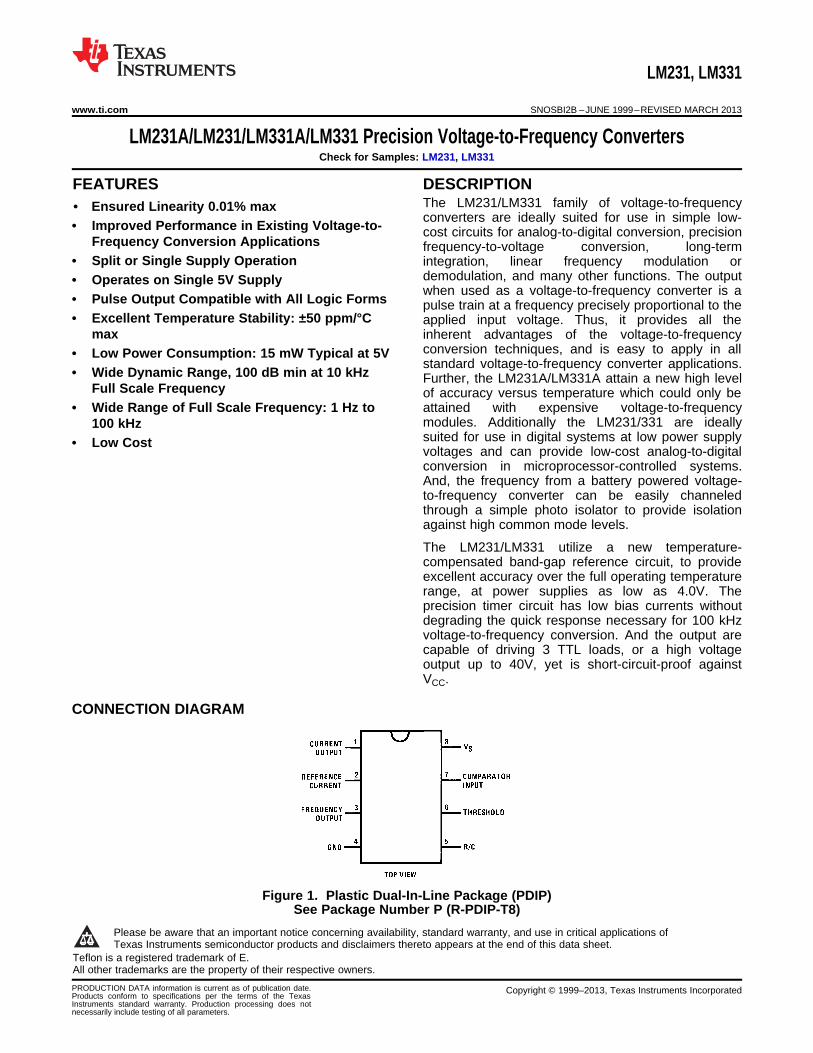
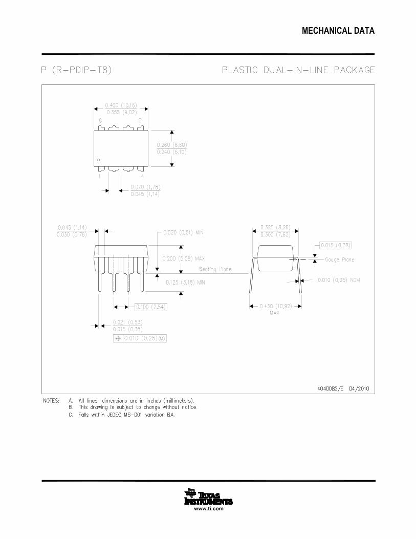
CONNECTION DIAGRAM
Figure 1. Plastic Dual-In-Line Package (PDIP)See Package Number P (R-PDIP-T8)
1
Please be aware that an important notice concerning availability, standard warranty, and use in critical applications ofTexas Instruments semiconductor products and disclaimers thereto appears at the end of this data sheet.
2Teflon is a registered trademark of E.3All other trademarks are the property of their respective owners.
PRODUCTION DATA information is current as of publication date. Copyright © 1999–2013, Texas Instruments IncorporatedProducts conform to specifications per the terms of the TexasInstruments standard warranty. Production processing does notnecessarily include testing of all parameters.
LM231, LM331
SNOSBI2B –JUNE 1999–REVISED MARCH 2013 www.ti.com
These devices have limited built-in ESD protection. The leads should be shorted together or the device placed in conductive foamduring storage or handling to prevent electrostatic damage to the MOS gates.
Absolute Maximum Ratings (1) (2) (3)
Supply Voltage, VS 40V
Output Short Circuit to Ground Continuous
Output Short Circuit to VCC Continuous
Input Voltage −0.2V to +VS
Package Dissipation at 25°C 1.25W (4)
Lead Temperature (Soldering, 10 sec.)
PDIP 260°C
ESD Susceptibility (5) 500V
(1) Absolute Maximum Ratings indicate limits beyond which damage to the device may occur. DC and AC electrical specifications do notapply when operating the device beyond its specified operating conditions.
(2) All voltages are measured with respect to GND = 0V, unless otherwise noted.(3) If Military/Aerospace specified devices are required, please contact the TI Sales Office/Distributors for availability and specifications.(4) The absolute maximum junction temperature (TJmax) for this device is 150°C. The maximum allowable power dissipation is dictated by
TJmax, the junction-to-ambient thermal resistance (θJA), and the ambient temperature TA, and can be calculated using the formulaPDmax = (TJmax - TA) / θJA. The values for maximum power dissipation will be reached only when the device is operated in a severefault condition (e.g., when input or output pins are driven beyond the power supply voltages, or the power supply polarity is reversed).Obviously, such conditions should always be avoided.
(5) Human body model, 100 pF discharged through a 1.5 kΩ resistor.
Operating Ratings (1)
Operating Ambient Temperature
LM231, LM231A −25°C to +85°C
LM331, LM331A 0°C to +70°C
Supply Voltage, VS +4V to +40V
(1) All voltages are measured with respect to GND = 0V, unless otherwise noted.
Package Thermal ResistancePackage θJ-A
8-Lead PDIP 100°C/W
Electrical CharacteristicsAll specifications apply in the circuit of Figure 16, with 4.0V ≤ VS ≤ 40V, TA=25°C, unless otherwise specified.
Parameter Conditions Min Typ Max Units
4.5V ≤ VS ≤ 20V ±0.003 ±0.01 % Full- ScaleVFC Non-Linearity (1)
TMIN ≤ TA ≤ TMAX ±0.006 ±0.02 % Full- Scale
VFC Non-Linearity in Circuit of Figure 15 VS = 15V, f = 10 Hz to 11 kHz ±0.024 ±0.14 %Full- Scale
Conversion Accuracy Scale Factor (Gain)
LM231, LM231A VIN = −10V, RS = 14 kΩ 0.95 1.00 1.05 kHz/V
LM331, LM331A 0.90 1.00 1.10 kHz/V
Temperature Stability of Gain
LM231/LM331 TMIN ≤ TA ≤ TMAX, 4.5V ≤ VS ≤ 20V ±30 ±150 ppm/°C
LM231A/LM331A ±20 ±50 ppm/°C
4.5V ≤ VS ≤ 10V 0.01 0.1 %/VChange of Gain with VS
10V ≤ VS ≤ 40V 0.006 0.06 %/V
Rated Full-Scale Frequency VIN = −10V 10.0 kHz
Gain Stability vs. Time (1000 Hours) TMIN ≤ TA ≤ TMAX ±0.02 % Full- Scale
(1) Nonlinearity is defined as the deviation of fOUT from VIN × (10 kHz/−10 VDC) when the circuit has been trimmed for zero error at 10 Hzand at 10 kHz, over the frequency range 1 Hz to 11 kHz. For the timing capacitor, CT, use NPO ceramic, Teflon®, or polystyrene.
2 Submit Documentation Feedback Copyright © 1999–2013, Texas Instruments Incorporated
Product Folder Links: LM231 LM331
LM231, LM331
www.ti.com SNOSBI2B –JUNE 1999–REVISED MARCH 2013
Electrical Characteristics (continued)All specifications apply in the circuit of Figure 16, with 4.0V ≤ VS ≤ 40V, TA=25°C, unless otherwise specified.
Parameter Conditions Min Typ Max Units
Over Range (Beyond Full-Scale) Frequency VIN = −11V 10 %
INPUT COMPARATOR
Offset Voltage ±3 ±10 mV
LM231/LM331 TMIN ≤ TA ≤ TMAX ±4 ±14 mV
LM231A/LM331A TMIN ≤ TA ≤ TMAX ±3 ±10 mV
Bias Current −80 −300 nA
Offset Current ±8 ±100 nA
VCC−2.Common-Mode Range TMIN ≤ TA ≤ TMAX −0.2 V0
TIMER
Timer Threshold Voltage, Pin 5 0.63 0.667 0.70 × VS
Input Bias Current, Pin 5 VS = 15V
All Devices 0V ≤ VPIN 5 ≤ 9.9V ±10 ±100 nA
LM231/LM331 VPIN 5 = 10V 200 1000 nA
LM231A/LM331A VPIN 5 = 10V 200 500 nA
VSAT PIN 5 (Reset) I = 5 mA 0.22 0.5 V
CURRENT SOURCE (Pin 1)
Output Current
LM231, LM231A RS = 14 kΩ, VPIN 1 = 0 126 135 144 μA
LM331, LM331A 116 136 156 μA
Change with Voltage 0V ≤ VPIN 1 ≤ 10V 0.2 1.0 μA
Current Source OFF Leakage
LM231, LM231A, LM331, LM331A 0.02 10.0 nA
All Devices TA = TMAX 2.0 50.0 nA
Operating Range of Current (Typical) (10 to 500) μA
REFERENCE VOLTAGE (Pin 2)
LM231, LM231A 1.76 1.89 2.02 VDC
LM331, LM331A 1.70 1.89 2.08 VDC
Stability vs. Temperature ±60 ppm/°C
Stability vs. Time, 1000 Hours ±0.1 %
LOGIC OUTPUT (Pin 3)
I = 5 mA 0.15 0.50 VVSAT I = 3.2 mA (2 TTL Loads), TMIN ≤ TA ≤ 0.10 0.40 VTMAX
OFF Leakage ±0.05 1.0 μA
SUPPLY CURRENT
VS = 5V 2.0 3.0 4.0 mALM231, LM231A
VS = 40V 2.5 4.0 6.0 mA
VS = 5V 1.5 3.0 6.0 mALM331, LM331A
VS = 40V 2.0 4.0 8.0 mA
Copyright © 1999–2013, Texas Instruments Incorporated Submit Documentation Feedback 3
Product Folder Links: LM231 LM331

LM231, LM331
SNOSBI2B –JUNE 1999–REVISED MARCH 2013 www.ti.com
FUNCTIONAL BLOCK DIAGRAM
Pin numbers apply to 8-pin packages only.
4 Submit Documentation Feedback Copyright © 1999–2013, Texas Instruments Incorporated
Product Folder Links: LM231 LM331
LM231, LM331
www.ti.com SNOSBI2B –JUNE 1999–REVISED MARCH 2013
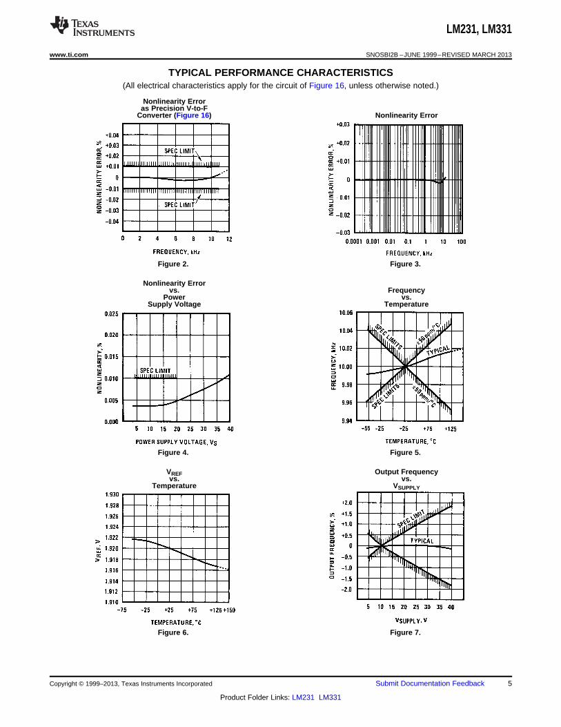
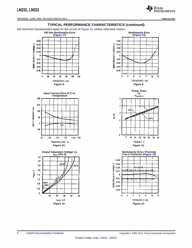
TYPICAL PERFORMANCE CHARACTERISTICS(All electrical characteristics apply for the circuit of Figure 16, unless otherwise noted.)
Nonlinearity Erroras Precision V-to-F
Converter (Figure 16) Nonlinearity Error
Figure 2. Figure 3.
Nonlinearity Errorvs. Frequency
Power vs.Supply Voltage Temperature
Figure 4. Figure 5.
VREF Output Frequencyvs. vs.
Temperature VSUPPLY
Figure 6. Figure 7.
Copyright © 1999–2013, Texas Instruments Incorporated Submit Documentation Feedback 5
Product Folder Links: LM231 LM331
LM231, LM331
SNOSBI2B –JUNE 1999–REVISED MARCH 2013 www.ti.com
TYPICAL PERFORMANCE CHARACTERISTICS (continued)(All electrical characteristics apply for the circuit of Figure 16, unless otherwise noted.)
100 kHz Nonlinearity Error Nonlinearity Error(Figure 17) (Figure 15)
Figure 8. Figure 9.
Power DrainInput Current (Pins 6,7) vs. vs.
Temperature VSUPPLY
Figure 10. Figure 11.
Output Saturation Voltage vs. Nonlinearity Error, PrecisionIOUT (Pin 3) F-to-V Converter (Figure 19)
Figure 12. Figure 13.
6 Submit Documentation Feedback Copyright © 1999–2013, Texas Instruments Incorporated
Product Folder Links: LM231 LM331

LM231, LM331
www.ti.com SNOSBI2B –JUNE 1999–REVISED MARCH 2013
APPLICATIONS INFORMATION
PRINCIPLES OF OPERATION
The LM231/331 are monolithic circuits designed for accuracy and versatile operation when applied as voltage-to-frequency (V-to-F) converters or as frequency-to-voltage (F-to-V) converters. A simplified block diagram of theLM231/331 is shown in Figure 14 and consists of a switched current source, input comparator, and 1-shot timer.
Figure 14. Simplified Block Diagram of Stand-AloneVoltage-to-Frequency Converter and
External Components
Simplified Voltage-to-Frequency Converter
The operation of these blocks is best understood by going through the operating cycle of the basic V-to-Fconverter, Figure 14, which consists of the simplified block diagram of the LM231/331 and the various resistorsand capacitors connected to it.
The voltage comparator compares a positive input voltage, V1, at pin 7 to the voltage, Vx, at pin 6. If V1 isgreater, the comparator will trigger the 1-shot timer. The output of the timer will turn ON both the frequencyoutput transistor and the switched current source for a period t=1.1 RtCt. During this period, the current i will flowout of the switched current source and provide a fixed amount of charge, Q = i × t, into the capacitor, CL. This willnormally charge Vx up to a higher level than V1. At the end of the timing period, the current i will turn OFF, andthe timer will reset itself.
Now there is no current flowing from pin 1, and the capacitor CL will be gradually discharged by RL until Vx fallsto the level of V1. Then the comparator will trigger the timer and start another cycle.
The current flowing into CL is exactly IAVE = i × (1.1×RtCt) × f, and the current flowing out of CL is exactly Vx/RL ≃VIN/RL. If VIN is doubled, the frequency will double to maintain this balance. Even a simple V-to-F converter canprovide a frequency precisely proportional to its input voltage over a wide range of frequencies.
Detail of Operation, Functional Block Diagram
The block diagram (FUNCTIONAL BLOCK DIAGRAM) shows a band gap reference which provides a stable 1.9VDC output. This 1.9 VDC is well regulated over a VS range of 3.9V to 40V. It also has a flat, low temperaturecoefficient, and typically changes less than ½% over a 100°C temperature change.
The current pump circuit forces the voltage at pin 2 to be at 1.9V, and causes a current i=1.90V/RS to flow. ForRs=14k, i=135 μA. The precision current reflector provides a current equal to i to the current switch. The currentswitch switches the current to pin 1 or to ground, depending upon the state of the RS flip-flop.
The timing function consists of an RS flip-flop and a timer comparator connected to the external RtCt network.When the input comparator detects a voltage at pin 7 higher than pin 6, it sets the RS flip-flop which turns ON thecurrent switch and the output driver transistor. When the voltage at pin 5 rises to ⅔ VCC, the timer comparatorcauses the RS flip-flop to reset. The reset transistor is then turned ON and the current switch is turned OFF.
Copyright © 1999–2013, Texas Instruments Incorporated Submit Documentation Feedback 7
Product Folder Links: LM231 LM331

LM231, LM331
SNOSBI2B –JUNE 1999–REVISED MARCH 2013 www.ti.com
However, if the input comparator still detects pin 7 higher than pin 6 when pin 5 crosses ⅔ VCC, the flip-flop willnot be reset, and the current at pin 1 will continue to flow, trying to make the voltage at pin 6 higher than pin 7.This condition will usually apply under start-up conditions or in the case of an overload voltage at signal input.During this sort of overload the output frequency will be 0. As soon as the signal is restored to the working range,the output frequency will be resumed.
The output driver transistor acts to saturate pin 3 with an ON resistance of about 50Ω. In case of over voltage,the output current is actively limited to less than 50 mA.
The voltage at pin 2 is regulated at 1.90 VDC for all values of i between 10 μA to 500 μA. It can be used as avoltage reference for other components, but care must be taken to ensure that current is not taken from it whichcould reduce the accuracy of the converter.
Basic Voltage-to-Frequency Converter (Figure 15)
The simple stand-alone V-to-F converter shown in Figure 15 includes all the basic circuitry of Figure 14 plus afew components for improved performance.
A resistor, RIN=100 kΩ ±10%, has been added in the path to pin 7, so that the bias current at pin 7 (−80 nAtypical) will cancel the effect of the bias current at pin 6 and help provide minimum frequency offset.
The resistance RS at pin 2 is made up of a 12 kΩ fixed resistor plus a 5 kΩ (cermet, preferably) gain adjustrheostat. The function of this adjustment is to trim out the gain tolerance of the LM231/331, and the tolerance ofRt, RL and Ct.
For best results, all the components should be stable low-temperature-coefficient components, such as metal-filmresistors. The capacitor should have low dielectric absorption; depending on the temperature characteristicsdesired, NPO ceramic, polystyrene, Teflon or polypropylene are best suited.
A capacitor CIN is added from pin 7 to ground to act as a filter for VIN. A value of 0.01 μF to 0.1 μF will beadequate in most cases; however, in cases where better filtering is required, a 1 μF capacitor can be used.When the RC time constants are matched at pin 6 and pin 7, a voltage step at VIN will cause a step change infOUT. If CIN is much less than CL, a step at VIN may cause fOUT to stop momentarily.
A 47Ω resistor, in series with the 1 μF CL, provides hysteresis, which helps the input comparator provide theexcellent linearity.
*Use stable components with low temperature coefficients. See APPLICATIONS INFORMATION.**0.1μF or 1μF, See PRINCIPLES OF OPERATION.
Figure 15. Simple Stand-Alone V-to-F Converterwith ±0.03% Typical Linearity (f = 10 Hz to 11 kHz)
8 Submit Documentation Feedback Copyright © 1999–2013, Texas Instruments Incorporated
Product Folder Links: LM231 LM331
LM231, LM331
www.ti.com SNOSBI2B –JUNE 1999–REVISED MARCH 2013
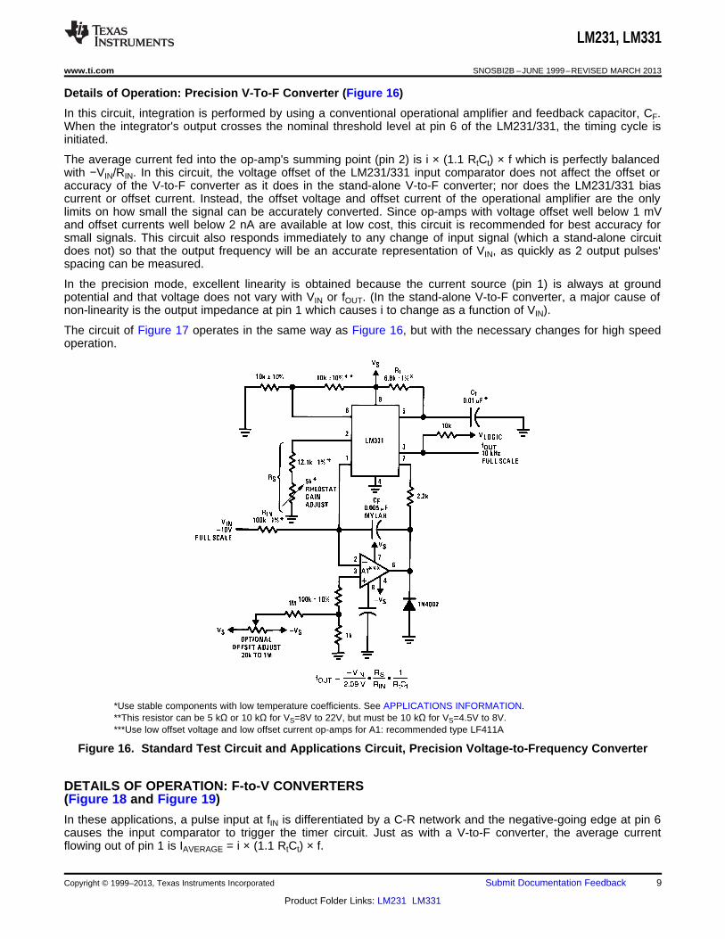
Details of Operation: Precision V-To-F Converter (Figure 16)
In this circuit, integration is performed by using a conventional operational amplifier and feedback capacitor, CF.When the integrator's output crosses the nominal threshold level at pin 6 of the LM231/331, the timing cycle isinitiated.
The average current fed into the op-amp's summing point (pin 2) is i × (1.1 RtCt) × f which is perfectly balancedwith −VIN/RIN. In this circuit, the voltage offset of the LM231/331 input comparator does not affect the offset oraccuracy of the V-to-F converter as it does in the stand-alone V-to-F converter; nor does the LM231/331 biascurrent or offset current. Instead, the offset voltage and offset current of the operational amplifier are the onlylimits on how small the signal can be accurately converted. Since op-amps with voltage offset well below 1 mVand offset currents well below 2 nA are available at low cost, this circuit is recommended for best accuracy forsmall signals. This circuit also responds immediately to any change of input signal (which a stand-alone circuitdoes not) so that the output frequency will be an accurate representation of VIN, as quickly as 2 output pulses'spacing can be measured.
In the precision mode, excellent linearity is obtained because the current source (pin 1) is always at groundpotential and that voltage does not vary with VIN or fOUT. (In the stand-alone V-to-F converter, a major cause ofnon-linearity is the output impedance at pin 1 which causes i to change as a function of VIN).
The circuit of Figure 17 operates in the same way as Figure 16, but with the necessary changes for high speedoperation.
*Use stable components with low temperature coefficients. See APPLICATIONS INFORMATION.**This resistor can be 5 kΩ or 10 kΩ for VS=8V to 22V, but must be 10 kΩ for VS=4.5V to 8V.***Use low offset voltage and low offset current op-amps for A1: recommended type LF411A
Figure 16. Standard Test Circuit and Applications Circuit, Precision Voltage-to-Frequency Converter
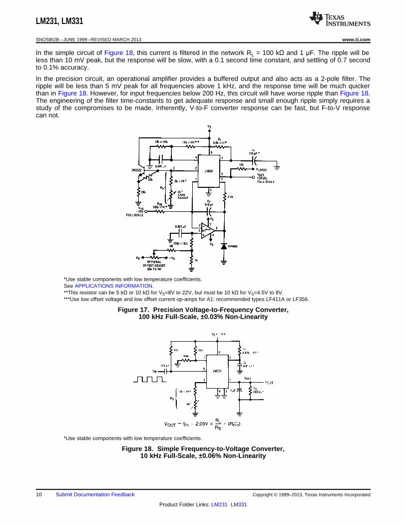
DETAILS OF OPERATION: F-to-V CONVERTERS(Figure 18 and Figure 19)
In these applications, a pulse input at fIN is differentiated by a C-R network and the negative-going edge at pin 6causes the input comparator to trigger the timer circuit. Just as with a V-to-F converter, the average currentflowing out of pin 1 is IAVERAGE = i × (1.1 RtCt) × f.
Copyright © 1999–2013, Texas Instruments Incorporated Submit Documentation Feedback 9
Product Folder Links: LM231 LM331
LM231, LM331
SNOSBI2B –JUNE 1999–REVISED MARCH 2013 www.ti.com
In the simple circuit of Figure 18, this current is filtered in the network RL = 100 kΩ and 1 μF. The ripple will beless than 10 mV peak, but the response will be slow, with a 0.1 second time constant, and settling of 0.7 secondto 0.1% accuracy.
In the precision circuit, an operational amplifier provides a buffered output and also acts as a 2-pole filter. Theripple will be less than 5 mV peak for all frequencies above 1 kHz, and the response time will be much quickerthan in Figure 18. However, for input frequencies below 200 Hz, this circuit will have worse ripple than Figure 18.The engineering of the filter time-constants to get adequate response and small enough ripple simply requires astudy of the compromises to be made. Inherently, V-to-F converter response can be fast, but F-to-V responsecan not.
*Use stable components with low temperature coefficients.See APPLICATIONS INFORMATION.**This resistor can be 5 kΩ or 10 kΩ for VS=8V to 22V, but must be 10 kΩ for VS=4.5V to 8V.***Use low offset voltage and low offset current op-amps for A1: recommended types LF411A or LF356.
Figure 17. Precision Voltage-to-Frequency Converter,100 kHz Full-Scale, ±0.03% Non-Linearity
*Use stable components with low temperature coefficients.
Figure 18. Simple Frequency-to-Voltage Converter,10 kHz Full-Scale, ±0.06% Non-Linearity
10 Submit Documentation Feedback Copyright © 1999–2013, Texas Instruments Incorporated
Product Folder Links: LM231 LM331

LM231, LM331
www.ti.com SNOSBI2B –JUNE 1999–REVISED MARCH 2013
*Use stable components with low temperature coefficients.
Figure 19. Precision Frequency-to-Voltage Converter,10 kHz Full-Scale with 2-Pole Filter, ±0.01%
Non-Linearity Maximum
*L14F-1, L14G-1 or L14H-1, photo transistor (General Electric Co.) or similar
Figure 20. Light Intensity to Frequency Converter
Figure 21. Temperature to Frequency Converter
Copyright © 1999–2013, Texas Instruments Incorporated Submit Documentation Feedback 11
Product Folder Links: LM231 LM331
LM231, LM331
SNOSBI2B –JUNE 1999–REVISED MARCH 2013 www.ti.com
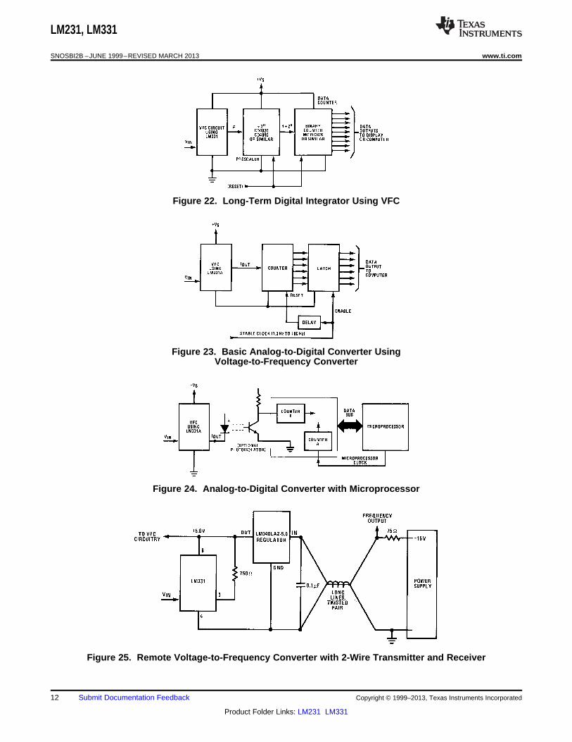
Figure 22. Long-Term Digital Integrator Using VFC
Figure 23. Basic Analog-to-Digital Converter UsingVoltage-to-Frequency Converter
Figure 24. Analog-to-Digital Converter with Microprocessor
Figure 25. Remote Voltage-to-Frequency Converter with 2-Wire Transmitter and Receiver
12 Submit Documentation Feedback Copyright © 1999–2013, Texas Instruments Incorporated
Product Folder Links: LM231 LM331

LM231, LM331
www.ti.com SNOSBI2B –JUNE 1999–REVISED MARCH 2013
Figure 26. Voltage-to-Frequency Converter with Square-Wave Output Using ÷ 2 Flip-Flop
Figure 27. Voltage-to-Frequency Converter with Isolators
Figure 28. Voltage-to-Frequency Converter with Isolators
Copyright © 1999–2013, Texas Instruments Incorporated Submit Documentation Feedback 13
Product Folder Links: LM231 LM331
LM231, LM331
SNOSBI2B –JUNE 1999–REVISED MARCH 2013 www.ti.com
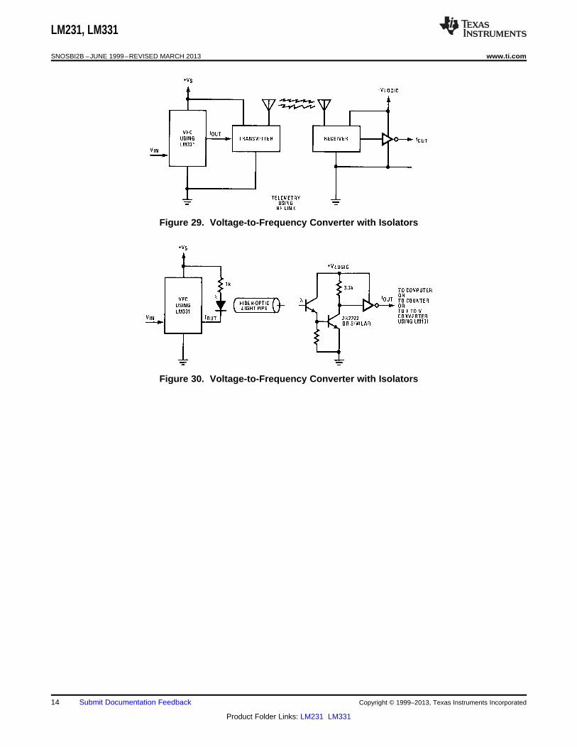
Figure 29. Voltage-to-Frequency Converter with Isolators
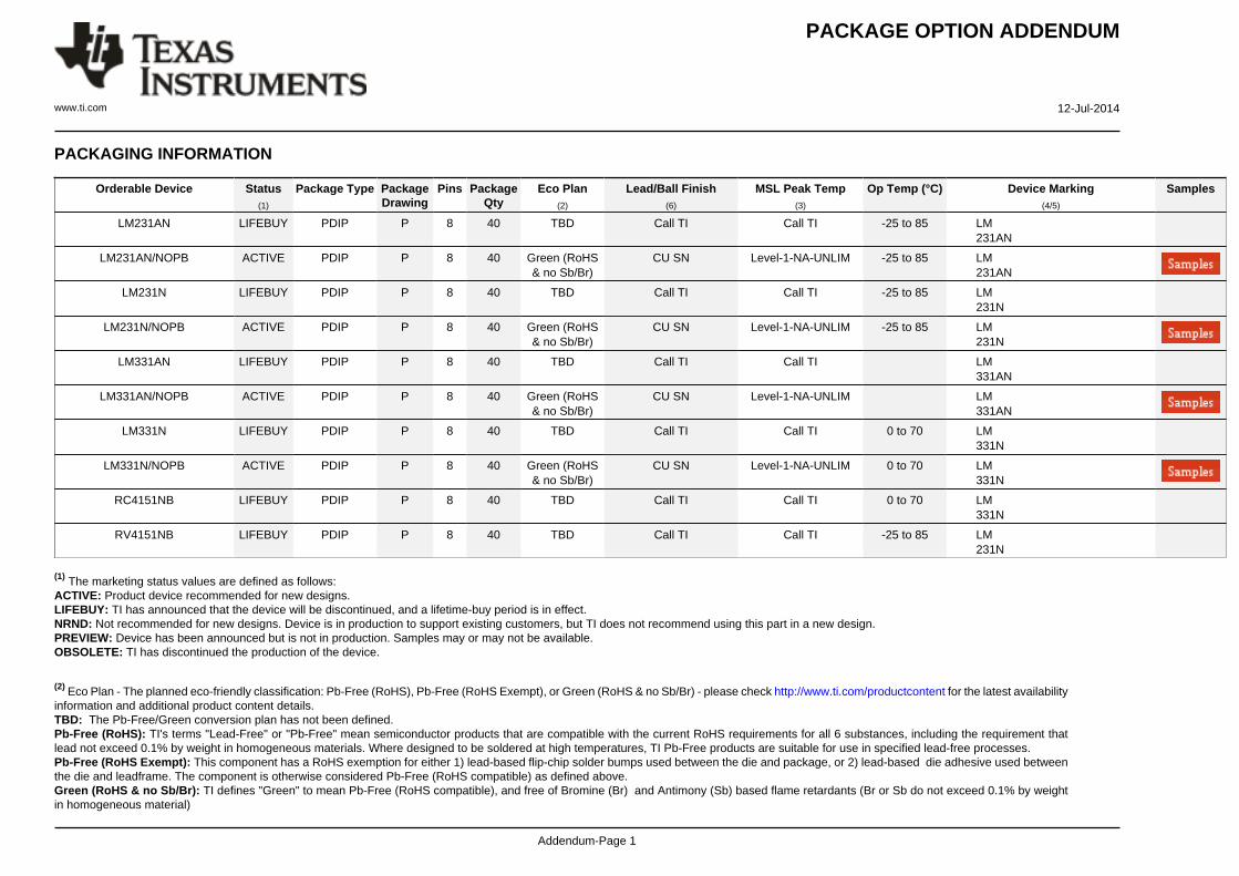
Figure 30. Voltage-to-Frequency Converter with Isolators
14 Submit Documentation Feedback Copyright © 1999–2013, Texas Instruments Incorporated
Product Folder Links: LM231 LM331

LM231, LM331
www.ti.com SNOSBI2B –JUNE 1999–REVISED MARCH 2013
Schematic Diagram
Copyright © 1999–2013, Texas Instruments Incorporated Submit Documentation Feedback 15
Product Folder Links: LM231 LM331

LM231, LM331
SNOSBI2B –JUNE 1999–REVISED MARCH 2013 www.ti.com
REVISION HISTORY
Changes from Revision A (March 2013) to Revision B Page
• Changed layout of National Data Sheet to TI format .......................................................................................................... 15
16 Submit Documentation Feedback Copyright © 1999–2013, Texas Instruments Incorporated
Product Folder Links: LM231 LM331
PACKAGE OPTION ADDENDUM
www.ti.com 12-Jul-2014
Addendum-Page 1
PACKAGING INFORMATION
Orderable Device Status(1)
Package Type PackageDrawing
Pins PackageQty
Eco Plan(2)
Lead/Ball Finish(6)
MSL Peak Temp(3)
Op Temp (°C) Device Marking(4/5)
Samples
LM231AN LIFEBUY PDIP P 8 40 TBD Call TI Call TI -25 to 85 LM231AN
LM231AN/NOPB ACTIVE PDIP P 8 40 Green (RoHS& no Sb/Br)
CU SN Level-1-NA-UNLIM -25 to 85 LM231AN
LM231N LIFEBUY PDIP P 8 40 TBD Call TI Call TI -25 to 85 LM231N
LM231N/NOPB ACTIVE PDIP P 8 40 Green (RoHS& no Sb/Br)
CU SN Level-1-NA-UNLIM -25 to 85 LM231N
LM331AN LIFEBUY PDIP P 8 40 TBD Call TI Call TI LM331AN
LM331AN/NOPB ACTIVE PDIP P 8 40 Green (RoHS& no Sb/Br)
CU SN Level-1-NA-UNLIM LM331AN
LM331N LIFEBUY PDIP P 8 40 TBD Call TI Call TI 0 to 70 LM331N
LM331N/NOPB ACTIVE PDIP P 8 40 Green (RoHS& no Sb/Br)
CU SN Level-1-NA-UNLIM 0 to 70 LM331N
RC4151NB LIFEBUY PDIP P 8 40 TBD Call TI Call TI 0 to 70 LM331N
RV4151NB LIFEBUY PDIP P 8 40 TBD Call TI Call TI -25 to 85 LM231N
(1) The marketing status values are defined as follows:ACTIVE: Product device recommended for new designs.LIFEBUY: TI has announced that the device will be discontinued, and a lifetime-buy period is in effect.NRND: Not recommended for new designs. Device is in production to support existing customers, but TI does not recommend using this part in a new design.PREVIEW: Device has been announced but is not in production. Samples may or may not be available.OBSOLETE: TI has discontinued the production of the device.
(2) Eco Plan - The planned eco-friendly classification: Pb-Free (RoHS), Pb-Free (RoHS Exempt), or Green (RoHS & no Sb/Br) - please check http://www.ti.com/productcontent for the latest availabilityinformation and additional product content details.TBD: The Pb-Free/Green conversion plan has not been defined.Pb-Free (RoHS): TI's terms "Lead-Free" or "Pb-Free" mean semiconductor products that are compatible with the current RoHS requirements for all 6 substances, including the requirement thatlead not exceed 0.1% by weight in homogeneous materials. Where designed to be soldered at high temperatures, TI Pb-Free products are suitable for use in specified lead-free processes.Pb-Free (RoHS Exempt): This component has a RoHS exemption for either 1) lead-based flip-chip solder bumps used between the die and package, or 2) lead-based die adhesive used betweenthe die and leadframe. The component is otherwise considered Pb-Free (RoHS compatible) as defined above.Green (RoHS & no Sb/Br): TI defines "Green" to mean Pb-Free (RoHS compatible), and free of Bromine (Br) and Antimony (Sb) based flame retardants (Br or Sb do not exceed 0.1% by weightin homogeneous material)
PACKAGE OPTION ADDENDUM
www.ti.com 12-Jul-2014
Addendum-Page 2
(3) MSL, Peak Temp. - The Moisture Sensitivity Level rating according to the JEDEC industry standard classifications, and peak solder temperature.
(4) There may be additional marking, which relates to the logo, the lot trace code information, or the environmental category on the device.
(5) Multiple Device Markings will be inside parentheses. Only one Device Marking contained in parentheses and separated by a "~" will appear on a device. If a line is indented then it is a continuationof the previous line and the two combined represent the entire Device Marking for that device.
(6) Lead/Ball Finish - Orderable Devices may have multiple material finish options. Finish options are separated by a vertical ruled line. Lead/Ball Finish values may wrap to two lines if the finishvalue exceeds the maximum column width.
Important Information and Disclaimer:The information provided on this page represents TI's knowledge and belief as of the date that it is provided. TI bases its knowledge and belief on informationprovided by third parties, and makes no representation or warranty as to the accuracy of such information. Efforts are underway to better integrate information from third parties. TI has taken andcontinues to take reasonable steps to provide representative and accurate information but may not have conducted destructive testing or chemical analysis on incoming materials and chemicals.TI and TI suppliers consider certain information to be proprietary, and thus CAS numbers and other limited information may not be available for release.
In no event shall TI's liability arising out of such information exceed the total purchase price of the TI part(s) at issue in this document sold by TI to Customer on an annual basis.

IMPORTANT NOTICETexas Instruments Incorporated and its subsidiaries (TI) reserve the right to make corrections, enhancements, improvements and otherchanges to its semiconductor products and services per JESD46, latest issue, and to discontinue any product or service per JESD48, latestissue. Buyers should obtain the latest relevant information before placing orders and should verify that such information is current andcomplete. All semiconductor products (also referred to herein as “components”) are sold subject to TI’s terms and conditions of salesupplied at the time of order acknowledgment.TI warrants performance of its components to the specifications applicable at the time of sale, in accordance with the warranty in TI’s termsand conditions of sale of semiconductor products. Testing and other quality control techniques are used to the extent TI deems necessaryto support this warranty. Except where mandated by applicable law, testing of all parameters of each component is not necessarilyperformed.TI assumes no liability for applications assistance or the design of Buyers’ products. Buyers are responsible for their products andapplications using TI components. To minimize the risks associated with Buyers’ products and applications, Buyers should provideadequate design and operating safeguards.TI does not warrant or represent that any license, either express or implied, is granted under any patent right, copyright, mask work right, orother intellectual property right relating to any combination, machine, or process in which TI components or services are used. Informationpublished by TI regarding third-party products or services does not constitute a license to use such products or services or a warranty orendorsement thereof. Use of such information may require a license from a third party under the patents or other intellectual property of thethird party, or a license from TI under the patents or other intellectual property of TI.Reproduction of significant portions of TI information in TI data books or data sheets is permissible only if reproduction is without alterationand is accompanied by all associated warranties, conditions, limitations, and notices. TI is not responsible or liable for such altereddocumentation. Information of third parties may be subject to additional restrictions.Resale of TI components or services with statements different from or beyond the parameters stated by TI for that component or servicevoids all express and any implied warranties for the associated TI component or service and is an unfair and deceptive business practice.TI is not responsible or liable for any such statements.Buyer acknowledges and agrees that it is solely responsible for compliance with all legal, regulatory and safety-related requirementsconcerning its products, and any use of TI components in its applications, notwithstanding any applications-related information or supportthat may be provided by TI. Buyer represents and agrees that it has all the necessary expertise to create and implement safeguards whichanticipate dangerous consequences of failures, monitor failures and their consequences, lessen the likelihood of failures that might causeharm and take appropriate remedial actions. Buyer will fully indemnify TI and its representatives against any damages arising out of the useof any TI components in safety-critical applications.In some cases, TI components may be promoted specifically to facilitate safety-related applications. With such components, TI’s goal is tohelp enable customers to design and create their own end-product solutions that meet applicable functional safety standards andrequirements. Nonetheless, such components are subject to these terms.No TI components are authorized for use in FDA Class III (or similar life-critical medical equipment) unless authorized officers of the partieshave executed a special agreement specifically governing such use.Only those TI components which TI has specifically designated as military grade or “enhanced plastic” are designed and intended for use inmilitary/aerospace applications or environments. Buyer acknowledges and agrees that any military or aerospace use of TI componentswhich have not been so designated is solely at the Buyer's risk, and that Buyer is solely responsible for compliance with all legal andregulatory requirements in connection with such use.TI has specifically designated certain components as meeting ISO/TS16949 requirements, mainly for automotive use. In any case of use ofnon-designated products, TI will not be responsible for any failure to meet ISO/TS16949.Products ApplicationsAudio www.ti.com/audio Automotive and Transportation www.ti.com/automotiveAmplifiers amplifier.ti.com Communications and Telecom www.ti.com/communicationsData Converters dataconverter.ti.com Computers and Peripherals www.ti.com/computersDLP® Products www.dlp.com Consumer Electronics www.ti.com/consumer-appsDSP dsp.ti.com Energy and Lighting www.ti.com/energyClocks and Timers www.ti.com/clocks Industrial www.ti.com/industrialInterface interface.ti.com Medical www.ti.com/medicalLogic logic.ti.com Security www.ti.com/securityPower Mgmt power.ti.com Space, Avionics and Defense www.ti.com/space-avionics-defenseMicrocontrollers microcontroller.ti.com Video and Imaging www.ti.com/videoRFID www.ti-rfid.comOMAP Applications Processors www.ti.com/omap TI E2E Community e2e.ti.comWireless Connectivity www.ti.com/wirelessconnectivity
Mailing Address: Texas Instruments, Post Office Box 655303, Dallas, Texas 75265Copyright © 2014, Texas Instruments Incorporated