lm2831 high-frequency 1.5-a load step-down dc-dc · pdf filelm2831 snvs422d–august...
TRANSCRIPT

100
90
80
70
60
500.1 1
EF
FIC
IEN
CY
(%)
LOAD (A)
"X"
GND
FBEN
VIN SWVIN = 5V
C1
R3
D1
L1
R2
R1
C2 C3
VO = 3.3V @ 1.5A
LM2831
Product
Folder
Sample &Buy
Technical
Documents
Tools &
Software
Support &Community
ReferenceDesign
LM2831SNVS422D –AUGUST 2006–REVISED SEPTEMBER 2015
LM2831 High-Frequency 1.5-A Load — Step-Down DC-DC Regulator1 Features 3 Description
The LM2831 regulator is a monolithic, high-1• Space-Saving SOT-23 Package
frequency, PWM step-down DC-DC converter in a 5-• Input Voltage Range of 3 V to 5.5 V pin SOT-23 and a 6-Pin WSON package. The• Output Voltage Range of 0.6 V to 4.5 V LM2831 provides all the active functions to provide
local DC-DC conversion with fast transient response• 1.5-A Output Currentand accurate regulation in the smallest possible PCB• High Switching Frequencie area. With a minimum of external components, the
– 1.6 MHz (LM2831X) LM2831 is easy to use. The ability to drive 1.5-Aloads with an internal 130-mΩ PMOS switch using– 0.55 MHz (LM2831Y)state-of-the-art 0.5-µm BiCMOS technology results in– 3 MHz (LM2831Z)the best power density available. The world-class
• 130-mΩ PMOS Switch control circuitry allows on-times as low as 30 ns, thus• 0.6-V, 2% Internal Voltage Reference supporting exceptionally high frequency conversion
over the entire 3 V to 5.5 V input operating range,• Internal Soft Startdown to the minimum output voltage of 0.6 V.• Current Mode, PWM Operation Switching frequency is internally set to 550 kHz, 1.6
• Thermal Shutdown MHz, or 3 MHz, allowing the use of extremely smallsurface mount inductors and chip capacitors. Even• Overvoltage Protectionthough the operating frequency is high, efficiencies ofup to 93% are easy to achieve. External shutdown is2 Applicationsincluded, featuring an ultra-low standby current of 30
• Local 5 V to Vcore Step-Down Converters nA. The LM2831 utilizes current-mode control andinternal compensation to provide high-performance• Core Power in HDDsregulation over a wide range of operating conditions.• Set-Top BoxesAdditional features include internal soft-start circuitry
• USB Powered Devices to reduce inrush current, pulse-by-pulse current limit,• DSL Modems thermal shutdown, and output overvoltage protection.
Device Information(1)
PART NUMBER PACKAGE BODY SIZE (NOM)WSON (6) 3.00 mm × 3.00 mm
LM2831SOT-23 (5) 1.60 mm × 2.90 mm
(1) For all available packages, see the orderable addendum atthe end of the data sheet.
Typical Application CircuitEfficiency vs Load
1
An IMPORTANT NOTICE at the end of this data sheet addresses availability, warranty, changes, use in safety-critical applications,intellectual property matters and other important disclaimers. PRODUCTION DATA.

LM2831SNVS422D –AUGUST 2006–REVISED SEPTEMBER 2015 www.ti.com
Table of Contents7.4 Device Functional Modes........................................ 111 Features .................................................................. 1
8 Application and Implementation ........................ 122 Applications ........................................................... 18.1 Application Information............................................ 123 Description ............................................................. 18.2 Typical Applications ............................................... 124 Revision History..................................................... 2
9 Power Supply Recommendations ...................... 255 Pin Configuration and Functions ......................... 310 Layout................................................................... 256 Specifications......................................................... 4
10.1 Layout Guidelines ................................................. 256.1 Absolute Maximum Ratings ...................................... 410.2 Layout Example .................................................... 296.2 ESD Ratings.............................................................. 4
11 Device and Documentation Support ................. 306.3 Recommended Operating Conditions....................... 411.1 Device Support...................................................... 306.4 Thermal Information .................................................. 411.2 Documentation Support ........................................ 306.5 Electrical Characteristics........................................... 511.3 Community Resources.......................................... 306.6 Typical Characteristics .............................................. 611.4 Trademarks ........................................................... 307 Detailed Description .............................................. 911.5 Electrostatic Discharge Caution............................ 307.1 Overview ................................................................... 911.6 Glossary ................................................................ 307.2 Functional Block Diagram ......................................... 9
12 Mechanical, Packaging, and Orderable7.3 Feature Description................................................... 9Information ........................................................... 30
4 Revision HistoryNOTE: Page numbers for previous revisions may differ from page numbers in the current version.
Changes from Revision C (April 2013) to Revision D Page
• Added ESD Ratings table, Feature Description section, Device Functional Modes, Application and Implementationsection, Power Supply Recommendations section, Layout section, Device and Documentation Support section, andMechanical, Packaging, and Orderable Information section. ................................................................................................ 1
Changes from Revision B (April 2013) to Revision C Page
• Changed layout of National Data Sheet to TI format ........................................................................................................... 24
2 Submit Documentation Feedback Copyright © 2006–2015, Texas Instruments Incorporated
Product Folder Links: LM2831

VIN SW
2
1
3
5
4EN FB
GND
1
2
3 4
6
5
ENFB
SW
DAP VINA
VIND
GND
LM2831www.ti.com SNVS422D –AUGUST 2006–REVISED SEPTEMBER 2015
5 Pin Configuration and Functions
NGG Package6-Pins WSON
Top View
DBV Package5-Pin SOT-23
Top View
Pin FunctionsPIN
I/O DESCRIPTIONNAME SOT-23 WSON
Enable control input. Logic high enables operation. Do not allow this pin toEN 4 6 I float or be greater than VIN + 0.3 V, or VINA + 0.3 V for WSON.FB 3 1 I Feedback pin. Connect to external resistor divider to set output voltage.
Signal and power ground pin. Place the bottom resistor of the feedbackGND 2 2 PWR network as close as possible to this pin.SW 1 3 O Output switch. Connect to the inductor and catch diode.VIN 5 — PWR Input supply voltageVINA — 5 PWR Control circuitry supply voltage. Connect VINA to VIND on PC board.VIND — 4 PWR Power input supplyDie Attach Connect to system ground for low thermal impedance, but it cannot be— DAP PWRPad used as a primary GND connection.
Copyright © 2006–2015, Texas Instruments Incorporated Submit Documentation Feedback 3
Product Folder Links: LM2831
LM2831SNVS422D –AUGUST 2006–REVISED SEPTEMBER 2015 www.ti.com
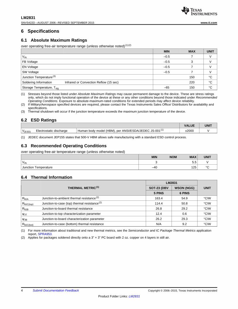
6 Specifications
6.1 Absolute Maximum Ratingsover operating free-air temperature range (unless otherwise noted) (1) (2)
MIN MAX UNITVIN –0.5 7 VFB Voltage –0.5 3 VEN Voltage –0.5 7 VSW Voltage –0.5 7 VJunction Temperature (3) 150 °CSoldering Information Infrared or Convection Reflow (15 sec) 220 °CStorage Temperature, Tstg –65 150 °C
(1) Stresses beyond those listed under Absolute Maximum Ratings may cause permanent damage to the device. These are stress ratingsonly, which do not imply functional operation of the device at these or any other conditions beyond those indicated under RecommendedOperating Conditions. Exposure to absolute-maximum-rated conditions for extended periods may affect device reliability.
(2) If Military/Aerospace specified devices are required, please contact the Texas Instruments Sales Office/ Distributors for availability andspecifications.
(3) Thermal shutdown will occur if the junction temperature exceeds the maximum junction temperature of the device.
6.2 ESD RatingsVALUE UNIT
V(ESD) Electrostatic discharge Human body model (HBM), per ANSI/ESDA/JEDEC JS-001 (1) ±2000 V
(1) JEDEC document JEP155 states that 500-V HBM allows safe manufacturing with a standard ESD control process.
6.3 Recommended Operating Conditionsover operating free-air temperature range (unless otherwise noted)
MIN NOM MAX UNITVIN 3 5.5 VJunction Temperature –40 125 °C
6.4 Thermal InformationLM2831
THERMAL METRIC (1) SOT-23 (DBV WSON (NGG) UNIT5 PINS 6 PINS
RθJA Junction-to-ambient thermal resistance (2) 163.4 54.9 °C/WRθJC(top) Junction-to-case (top) thermal resistance (2) 114.4 50.8 °C/WRθJB Junction-to-board thermal resistance 26.8 29.2 °C/WψJT Junction-to-top characterization parameter 12.4 0.6 °C/WψJB Junction-to-board characterization parameter 26.2 29.3 °C/WRθJC(bot) Junction-to-case (bottom) thermal resistance N/A 9.2 °C/W
(1) For more information about traditional and new thermal metrics, see the Semiconductor and IC Package Thermal Metrics applicationreport, SPRA953.
(2) Applies for packages soldered directly onto a 3” × 3” PC board with 2 oz. copper on 4 layers in still air.
4 Submit Documentation Feedback Copyright © 2006–2015, Texas Instruments Incorporated
Product Folder Links: LM2831

LM2831www.ti.com SNVS422D –AUGUST 2006–REVISED SEPTEMBER 2015
6.5 Electrical CharacteristicsVIN = 5 V unless otherwise indicated under the Test Conditions column. Limits are for TJ = 25°C. Minimum and Maximumlimits are specified through test, design, or statistical correlation. Typical values represent the most likely parametric norm atTJ = 25°C, and are provided for reference purposes only.
PARAMETER TEST CONDITIONS MIN TYP MAX UNIT
WSON and SOT-23 TJ = 25°C 0.600VFB Feedback Voltage VPackage –40°C to 125°C 0.588 0.612
ΔVFB/VIN Feedback Voltage Line Regulation VIN = 3 V to 5 V 0.02 %/V
IB Feedback Input Bias Current TJ = 25°C 0.1nA
–40°C to 125°C 100
VIN Rising TJ = 25°C 2.73V
–40°C to 125°C 2.90Undervoltage Lockout
UVLO VIN Falling TJ = 25°C 2.3V
–40°C to 125°C 1.85
UVLO Hysteresis 0.43 V
LM2831-X TJ = 25°C 1.6
–40°C to 125°C 1.2 1.95
LM2831-Y TJ = 25°C 0.55FSW Switching Frequency MHz
–40°C to 125°C 0.4 0.7
LM2831-Z TJ = 25°C 3
–40°C to 125°C 2.25 3.75
LM2831-X TJ = 25°C 94%
–40°C to 125°C 86%
LM2831-Y TJ = 25°C 96%DMAX Maximum Duty Cycle
–40°C to 125°C 90%
LM2831-Z TJ = 25°C 90%
–40°C to 125°C 82%
LM2831-X 5%
DMIN Minimum Duty Cycle LM2831-Y 2%
LM2831-Z 7%
WSON Package 150
RDS(ON) Switch On Resistance SOT-23 Package TJ = 25°C 130 mΩ
–40°C to 125°C 195
ICL Switch Current Limit VIN = 3.3 V TJ = 25°C 2.5A
–40°C to 125°C 1.8
Shutdown Threshold Voltage –40°C to 125°C 0.4VEN_TH V
Enable Threshold Voltage –40°C to 125°C 1.8
ISW Switch Leakage 100 nA
IEN Enable Pin Current Sink/Source 100 nA
LM2831X VFB = 0.55 TJ = 25°C 3.3
–40°C to 125°C 5
LM2831Y VFB = 0.55 TJ = 25°C 2.8Quiescent Current (switching) mA
IQ –40°C to 125°C 4.5
LM2831Z VFB = 0.55 TJ = 25°C 4.3
–40°C to 125°C 6.5
Quiescent Current (shutdown) All Options VEN = 0 V 30 nA
TSD Thermal Shutdown Temperature 165 °C
Copyright © 2006–2015, Texas Instruments Incorporated Submit Documentation Feedback 5
Product Folder Links: LM2831
-45 -40 -10 20 50 80 110 125 130
TEMPERATURE (ºC)
OS
CIL
LAT
OR
FR
EQ
UE
NC
Y (
MH
z)
0.46
0.48
0.50
0.52
0.54
0.56
0.58
0.60
-45 -40 -10 20 50 80 110 125 130
TEMPERATURE (ºC)
OS
CIL
LAT
OR
FR
EQ
UE
NC
Y (
MH
z)
1.36
1.41
1.46
1.51
1.56
1.61
1.66
1.71
1.76
1.81
1.794
1.796
1.798
1.800
1.802
1.804
1.806
0.25 0.5 0.75 1 1.25 1.5
LOAD (A)
OU
TP
UT
(V
)
03.297
3.298
3.299
3.300
3.301
3.302
0 0.25 0.5 0.75 1 1.25 1.5
LOAD (A)
OU
TP
UT
(V
)
1.796
1.797
1.798
1.799
1.800
1.801
1.802
1.803
1.804
0 0.25 0.5 0.75 1 1.25 1.5
LOAD (A)
OU
TP
UT
(V
)
LM2831SNVS422D –AUGUST 2006–REVISED SEPTEMBER 2015 www.ti.com
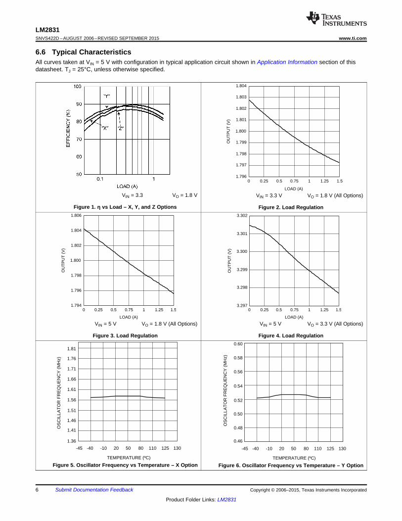
6.6 Typical CharacteristicsAll curves taken at VIN = 5 V with configuration in typical application circuit shown in Application Information section of thisdatasheet. TJ = 25°C, unless otherwise specified.
VIN = 3.3 VO = 1.8 V VIN = 3.3 V VO = 1.8 V (All Options)
Figure 1. η vs Load – X, Y, and Z Options Figure 2. Load Regulation
VIN = 5 V VO = 1.8 V (All Options) VIN = 5 V VO = 3.3 V (All Options)
Figure 3. Load Regulation Figure 4. Load Regulation
Figure 5. Oscillator Frequency vs Temperature – X Option Figure 6. Oscillator Frequency vs Temperature – Y Option
6 Submit Documentation Feedback Copyright © 2006–2015, Texas Instruments Incorporated
Product Folder Links: LM2831

-45 -40 -10 20 50 80 110 125 130
TEMPERATURE (ºC)
3.0
3.1
3.2
3.3
3.4
3.5
3.6
I Q (
mA
)
-45 -40 -10 20 50 80 110 125 130
TEMPERATURE (°C)
2.15
2.2
2.25
2.3
2.35
2.4
2.45
2.5
2.55
2.6
2.65
I Q (
mA
)
-45 -40 -10 20 50 80 110 125 130
TEMPERATURE (°C)
2100
2200
2300
2400
2500
2600
2700
2800
2900
CU
RR
EN
T L
IMIT
(m
A)
-45 -40 -10 20 50 80 110 125 130
TEMPERATURE (ºC)
OS
CIL
LAT
OR
FR
EQ
UE
NC
Y (
MH
z)
2.55
2.65
2.75
2.85
2.95
3.05
3.15
3.25
3.35
3.45
LM2831www.ti.com SNVS422D –AUGUST 2006–REVISED SEPTEMBER 2015
Typical Characteristics (continued)All curves taken at VIN = 5 V with configuration in typical application circuit shown in Application Information section of thisdatasheet. TJ = 25°C, unless otherwise specified.
VIN = 3.3 V
Figure 7. Oscillator Frequency vs Temperature – Z Option Figure 8. Current Limit vs Temperature
Figure 9. RDSON vs Temperature (WSON Package) Figure 10. RDSON vs Temperature (SOT-23 Package)
Figure 12. LM2831Y IQ (Quiescent Current)Figure 11. LM2831X IQ (Quiescent Current)
Copyright © 2006–2015, Texas Instruments Incorporated Submit Documentation Feedback 7
Product Folder Links: LM2831

-45 -40 -10 20 50 80 110 125 130
TEMPERATURE (ºC)
FE
EB
AC
K V
OLT
AG
E (
V)
0.590
0.595
0.600
0.605
0.610
-45 -40 -10 20 50 80 110 125 130
TEMPERATURE (ºC)
4.0
4.1
4.2
4.3
4.4
4.5
4.6
I Q (
mA
)
LM2831SNVS422D –AUGUST 2006–REVISED SEPTEMBER 2015 www.ti.com
Typical Characteristics (continued)All curves taken at VIN = 5 V with configuration in typical application circuit shown in Application Information section of thisdatasheet. TJ = 25°C, unless otherwise specified.
VO = 1.8 V IO = 500 mA
Figure 14. Line RegulationFigure 13. LM2831Z IQ (Quiescent Current)
VIN = 5 V VO = 1.2 V at 1 A
Figure 15. VFB vs Temperature Figure 16. Gain vs Frequency
VIN = 5 V VO = 1.2 V at 1 A
Figure 17. Phase Plot vs Frequency
8 Submit Documentation Feedback Copyright © 2006–2015, Texas Instruments Incorporated
Product Folder Links: LM2831

cv
+
-+
-
S
R
R
Q
+
-
GND
FB
SW
VINEN
+
-
+ -
DRIVER
ArtificialRamp
SHDNThermal
SHDNOVP
1.6 MHz
CompInternal -
SENSEI
LIMITI
LDOInternal -STARTSOFT-
PFET
SENSEI
ENABLE and UVLO
15.1 x REFV
Control Logic
VREF = 0.6V
LM2831www.ti.com SNVS422D –AUGUST 2006–REVISED SEPTEMBER 2015
7 Detailed Description
7.1 OverviewThe LM2831 device is a constant-frequency PWM buck regulator IC that delivers a 1.5-A load current. Theregulator has a preset switching frequency of 550 kHz, 1.6 MHz, or 3 MHz. This high-frequency allows theLM2831 to operate with small surface mount capacitors and inductors, resulting in a DC-DC converter thatrequires a minimum amount of board space. The LM2831 is internally compensated, so the device is simple touse and requires few external components.
7.2 Functional Block Diagram
7.3 Feature Description
7.3.1 Theory of OperationThe LM2831 uses current-mode control to regulate the output voltage. The following operating description of theLM2831 will refer to Functional Block Diagram and to the waveforms in Figure 18. The LM2831 supplies aregulated output voltage by switching the internal PMOS control switch at constant-frequency and variable dutycycle. A switching cycle begins at the falling edge of the reset pulse generated by the internal oscillator. Whenthis pulse goes low, the output control logic turns on the internal PMOS control switch. During this on-time, theSW pin voltage (VSW) swings up to approximately VIN, and the inductor current (IL) increases with a linear slope.IL is measured by the current sense amplifier, which generates an output proportional to the switch current. Thesense signal is summed with the regulator’s corrective ramp and compared to the error amplifier’s output, which
Copyright © 2006–2015, Texas Instruments Incorporated Submit Documentation Feedback 9
Product Folder Links: LM2831

0
0
VIN
VD
TON
t
t
Inductor
Current
D = TON/TSW
VSW
TOFF
TSWIL
IPK
SW
Voltage
LM2831SNVS422D –AUGUST 2006–REVISED SEPTEMBER 2015 www.ti.com
Feature Description (continued)is proportional to the difference between the feedback voltage and VREF. When the PWM comparator output goeshigh, the output switch turns off until the next switching cycle begins. During the switch off-time, inductor currentdischarges through the Schottky catch diode, which forces the SW pin to swing below ground by the forwardvoltage (VD) of the Schottky catch diode. The regulator loop adjusts the duty cycle (D) to maintain a constantoutput voltage.
Figure 18. Typical Waveforms
7.3.2 Soft StartThis function forces VOUT to increase at a controlled rate during start up. During soft start, the error amplifier’sreference voltage ramps from 0 V to its nominal value of 0.6 V in approximately 600 µs. This forces the regulatoroutput to ramp up in a controlled fashion, which helps reduce inrush current.
7.3.3 Output Overvoltage ProtectionThe overvoltage comparator compares the FB pin voltage to a voltage that is 15% higher than the internalreference VREF. Once the FB pin voltage goes 15% above the internal reference, the internal PMOS controlswitch is turned off, which allows the output voltage to decrease toward regulation.
7.3.4 Undervoltage LockoutUndervoltage lockout (UVLO) prevents the LM2831 from operating until the input voltage exceeds 2.73 V(typical). The UVLO threshold has approximately 430 mV of hysteresis, so the part will operate until VIN dropsbelow 2.3 V (typical). Hysteresis prevents the part from turning off during power up if VIN is non-monotonic.
7.3.5 Current LimitThe LM2831 uses cycle-by-cycle current limiting to protect the output switch. During each switching cycle, acurrent limit comparator detects if the output switch current exceeds 2.5 A (typical), and turns off the switch untilthe next switching cycle begins.
7.3.6 Thermal ShutdownThermal shutdown limits total power dissipation by turning off the output switch when the IC junction temperatureexceeds 165°C. After thermal shutdown occurs, the output switch doesn’t turn on until the junction temperaturedrops to approximately 150°C.
10 Submit Documentation Feedback Copyright © 2006–2015, Texas Instruments Incorporated
Product Folder Links: LM2831

LM2831www.ti.com SNVS422D –AUGUST 2006–REVISED SEPTEMBER 2015
7.4 Device Functional ModesThe LM2831 has an enable pin (EN) control Input. A logic high enables device operation. Do not float this pin orlet this pin be greater than VIN + 0.3 V for the SOT package option, or VINA + 0.3 V for the WSON packageoption.
Copyright © 2006–2015, Texas Instruments Incorporated Submit Documentation Feedback 11
Product Folder Links: LM2831

GND
FBEN
VIN SWVIN = 5V
C1
R3
D1
L1LM2831
R2
R1
C2
VO = 1.2V @ 1.5A
LM2831SNVS422D –AUGUST 2006–REVISED SEPTEMBER 2015 www.ti.com
8 Application and Implementation
NOTEInformation in the following applications sections is not part of the TI componentspecification, and TI does not warrant its accuracy or completeness. TI’s customers areresponsible for determining suitability of components for their purposes. Customers shouldvalidate and test their design implementation to confirm system functionality.
8.1 Application InformationThe LM2831 device will operate with input voltage range from 3 V to 5.5 V and provide a regulated outputvoltage. This device is optimized for high-efficiency operation with minimum number of external components. Forcomponent selection, see Detailed Design Procedure.
8.2 Typical Applications
8.2.1 LM2831X Design Example 1
Figure 19. LM2831X (1.6 MHz): VIN = 5 V, VO = 1.2 V at 1.5 A
8.2.1.1 Design RequirementsThe device must be able to operate at any voltage within the recommended operating range. Load current mustbe defined to properly size the inductor, input, and output capacitors. Inductor should be able to handle fullexpected load current as well as the peak current generated during load transients and start up. Inrush current atstart-up will depend on the output capacitor selection. More details are provided in Detailed Design Procedure.
12 Submit Documentation Feedback Copyright © 2006–2015, Texas Instruments Incorporated
Product Folder Links: LM2831
IN OUT L
S
V V 2 i
L DT
- D=
t
Li'
OUTI
STSDT
L
VOUT
L
- VOUTVIN
OUT D
IN D SW
V VD
V V V
+
=
+ -
OUT
IN
VD
V=
LM2831www.ti.com SNVS422D –AUGUST 2006–REVISED SEPTEMBER 2015
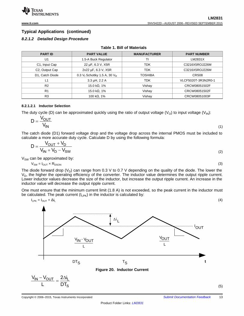
Typical Applications (continued)8.2.1.2 Detailed Design Procedure
Table 1. Bill of MaterialsPART ID PART VALUE MANUFACTURER PART NUMBER
U1 1.5-A Buck Regulator TI LM2831XC1, Input Cap 22 µF, 6.3 V, X5R TDK C3216X5ROJ226M
C2, Output Cap 2x22 µF, 6.3 V, X5R TDK C3216X5ROJ226MD1, Catch Diode 0.3 Vf Schottky 1.5 A, 30 VR TOSHIBA CRS08
L1 3.3 µH, 2.2 A TDK VLCF5020T-3R3N2R0-1R2 15.0 kΩ, 1% Vishay CRCW08051502FR1 15.0 kΩ, 1% Vishay CRCW08051502FR3 100 kΩ, 1% Vishay CRCW08051003F
8.2.1.2.1 Inductor Selection
The duty cycle (D) can be approximated quickly using the ratio of output voltage (VO) to input voltage (VIN):
(1)
The catch diode (D1) forward voltage drop and the voltage drop across the internal PMOS must be included tocalculate a more accurate duty cycle. Calculate D by using the following formula:
(2)
VSW can be approximated by:VSW = IOUT × RDSON (3)
The diode forward drop (VD) can range from 0.3 V to 0.7 V depending on the quality of the diode. The lower theVD, the higher the operating efficiency of the converter. The inductor value determines the output ripple current.Lower inductor values decrease the size of the inductor, but increase the output ripple current. An increase in theinductor value will decrease the output ripple current.
One must ensure that the minimum current limit (1.8 A) is not exceeded, so the peak current in the inductor mustbe calculated. The peak current (ILPK) in the inductor is calculated by:
ILPK = IOUT + ΔiL (4)
Figure 20. Inductor Current
(5)
Copyright © 2006–2015, Texas Instruments Incorporated Submit Documentation Feedback 13
Product Folder Links: LM2831

RMS _IN OUTI I D(1 D)= ´ -
22
RMS _IN OUT
iI D I (1 D)
3
é ùD- +ê ú
ê úë û
S
S
1T
f=
SIN OUT
L
DTL V V
2 i
æ ö= ´ -ç ÷
Dè ø
LM2831SNVS422D –AUGUST 2006–REVISED SEPTEMBER 2015 www.ti.com
In general,ΔiL = 0.1 × (IOUT) → 0.2 × (IOUT) (6)
If ΔiL = 20% of 1.50 A, the peak current in the inductor will be 1.8 A. The minimum ensured current limit over alloperating conditions is 1.8 A. One can either reduce ΔiL, or make the engineering judgment that zero margin willbe safe enough. The typical current limit is 2.5 A.
The LM2831 operates at frequencies allowing the use of ceramic output capacitors without compromisingtransient response. Ceramic capacitors allow higher inductor ripple without significantly increasing output ripple.See the Output Capacitor section for more details on calculating output voltage ripple. Now that the ripple currentis determined, the inductance is calculated by:
(7)
Where:
(8)
When selecting an inductor, make sure that it is capable of supporting the peak output current without saturating.Inductor saturation will result in a sudden reduction in inductance and prevent the regulator from operatingcorrectly. Because of the speed of the internal current limit, the peak current of the inductor need only bespecified for the required maximum output current. For example, if the designed maximum output current is 1 Aand the peak current is 1.25 A, then the inductor should be specified with a saturation current limit of > 1.25 A.There is no need to specify the saturation or peak current of the inductor at the 2.5-A typical switch current limit.The difference in inductor size is a factor of 5. Because of the operating frequency of the LM2831, ferrite basedinductors are preferred to minimize core losses. This presents little restriction since the variety of ferrite-basedinductors is huge. Lastly, inductors with lower series resistance (RDCR) will provide better operating efficiency. Forrecommended inductors, see LM2831X Design Example 2 through LM2831X Buck Converter and VoltageDouble Circuit With LDO Follower Design Example 9.
8.2.1.2.2 Input Capacitor
An input capacitor is necessary to ensure that VIN does not drop excessively during switching transients. Theprimary specifications of the input capacitor are capacitance, voltage, RMS current rating, and ESL (EquivalentSeries Inductance). The recommended input capacitance is 22 µF. The input voltage rating is specifically statedby the capacitor manufacturer. Make sure to check any recommended deratings and also verify if there is anysignificant change in capacitance at the operating input voltage and the operating temperature. The inputcapacitor maximum RMS input current rating (IRMS-IN) must be greater than:
(9)
Neglecting inductor ripple simplifies the above equation to:
(10)
It can be shown from the above equation that maximum RMS capacitor current occurs when D = 0.5. Alwayscalculate the RMS at the point where the duty cycle D is closest to 0.5. The ESL of an input capacitor is usuallydetermined by the effective cross sectional area of the current path. A large leaded capacitor will have high ESLand a 0805 ceramic chip capacitor will have very low ESL. At the operating frequencies of the LM2831, leadedcapacitors may have an ESL so large that the resulting impedance (2πfL) will be higher than that required toprovide stable operation. As a result, surface mount capacitors are strongly recommended.
Sanyo POSCAP, Tantalum or Niobium, Panasonic SP, and multilayer ceramic capacitors (MLCC) are all goodchoices for both input and output capacitors and have very low ESL. For MLCCs it is recommended to use X7Ror X5R type capacitors due to their tolerance and temperature characteristics. Consult capacitor manufacturerdata sheets to see how rated capacitance varies over operating conditions.
14 Submit Documentation Feedback Copyright © 2006–2015, Texas Instruments Incorporated
Product Folder Links: LM2831

x R2R1 =VREF
VOUT- 1
OUT L ESR
SW OUT
1V I R
8 F C
æ ö= D +ç ÷
´ ´è ø
LM2831www.ti.com SNVS422D –AUGUST 2006–REVISED SEPTEMBER 2015
8.2.1.2.3 Output Capacitor
The output capacitor is selected based upon the desired output ripple and transient response. The initial currentof a load transient is provided mainly by the output capacitor. The output ripple of the converter is:
(11)
When using MLCCs, the ESR is typically so low that the capacitive ripple may dominate. When this occurs, theoutput ripple will be approximately sinusoidal and 90° phase shifted from the switching action. Given theavailability and quality of MLCCs and the expected output voltage of designs using the LM2831, there is really noneed to review any other capacitor technologies. Another benefit of ceramic capacitors is their ability to bypasshigh frequency noise. A certain amount of switching edge noise will couple through parasitic capacitances in theinductor to the output. A ceramic capacitor will bypass this noise while a tantalum will not. Since the outputcapacitor is one of the two external components that control the stability of the regulator control loop, mostapplications will require a minimum of 22 µF of output capacitance. Capacitance often, but not always, can beincreased significantly with little detriment to the regulator stability. Like the input capacitor, recommendedmultilayer ceramic capacitors are X7R or X5R types.
8.2.1.2.4 Catch Diode
The catch diode (D1) conducts during the switch off-time. A Schottky diode is recommended for its fast switchingtimes and low forward voltage drop. The catch diode should be chosen so that its current rating is greater than:
ID1 = IOUT × (1-D) (12)
The reverse breakdown rating of the diode must be at least the maximum input voltage plus appropriate margin.To improve efficiency, choose a Schottky diode with a low forward voltage drop.
8.2.1.2.5 Output Voltage
The output voltage is set using the following equation where R2 is connected between the FB pin and GND, andR1 is connected between VO and the FB pin. A good value for R2 is 10 kΩ. When designing a unity gainconverter (Vo = 0.6 V), R1 should be from 0 Ω to 100 Ω, and R2 should be equal or greater than 10 kΩ.
(13)VREF = 0.60 V (14)
Copyright © 2006–2015, Texas Instruments Incorporated Submit Documentation Feedback 15
Product Folder Links: LM2831

LM2831SNVS422D –AUGUST 2006–REVISED SEPTEMBER 2015 www.ti.com
8.2.1.3 Application CurvesSee Typical Characteristics.
VIN = 5 V VO = 1.8 V and 3.3 V VIN = 5 V VO = 1.8 V and 3.3 V
Figure 21. η vs Load – X Option Figure 22. η vs Load – Y Option
VIN = 5 V VO = 1.8 V and 3.3 V
Figure 23. η vs Load – Z Option
16 Submit Documentation Feedback Copyright © 2006–2015, Texas Instruments Incorporated
Product Folder Links: LM2831

GND
FBEN
VIN SWVIN = 5V
C1
R3
D1
L1LM2831
R2
R1
C2
VO = 0.6V @ 1.5A
LM2831www.ti.com SNVS422D –AUGUST 2006–REVISED SEPTEMBER 2015
8.2.2 LM2831X Design Example 2
Figure 24. LM2831X (1.6 MHz): VIN = 5 V, VO = 0.6 V at 1.5 A
Table 2. Bill of MaterialsPART ID PART VALUE MANUFACTURER PART NUMBER
U1 1.5-A Buck Regulator TI LM2831XC1, Input Capacitor 22 µF, 6.3 V, X5R TDK C3216X5ROJ226M
C2, Output Capacitor 2x22 µF, 6.3 V, X5R TDK C3216X5ROJ226MD1, Catch Diode 0.3 Vf Schottky 1.5 A, 30 VR TOSHIBA CRS08
L1 3.3 µH, 2.2 A TDK VLCF5020T- 3R3N2R0-1R2 10.0 kΩ, 1% Vishay CRCW08051000FR1 0 ΩR3 100 kΩ, 1% Vishay CRCW08051003F
Copyright © 2006–2015, Texas Instruments Incorporated Submit Documentation Feedback 17
Product Folder Links: LM2831
GND
FBEN
VIN SWVIN = 5V
C1
R3
D1
L1LM2831
R2
R1
C2
VO = 3.3V @ 1.5A
LM2831SNVS422D –AUGUST 2006–REVISED SEPTEMBER 2015 www.ti.com
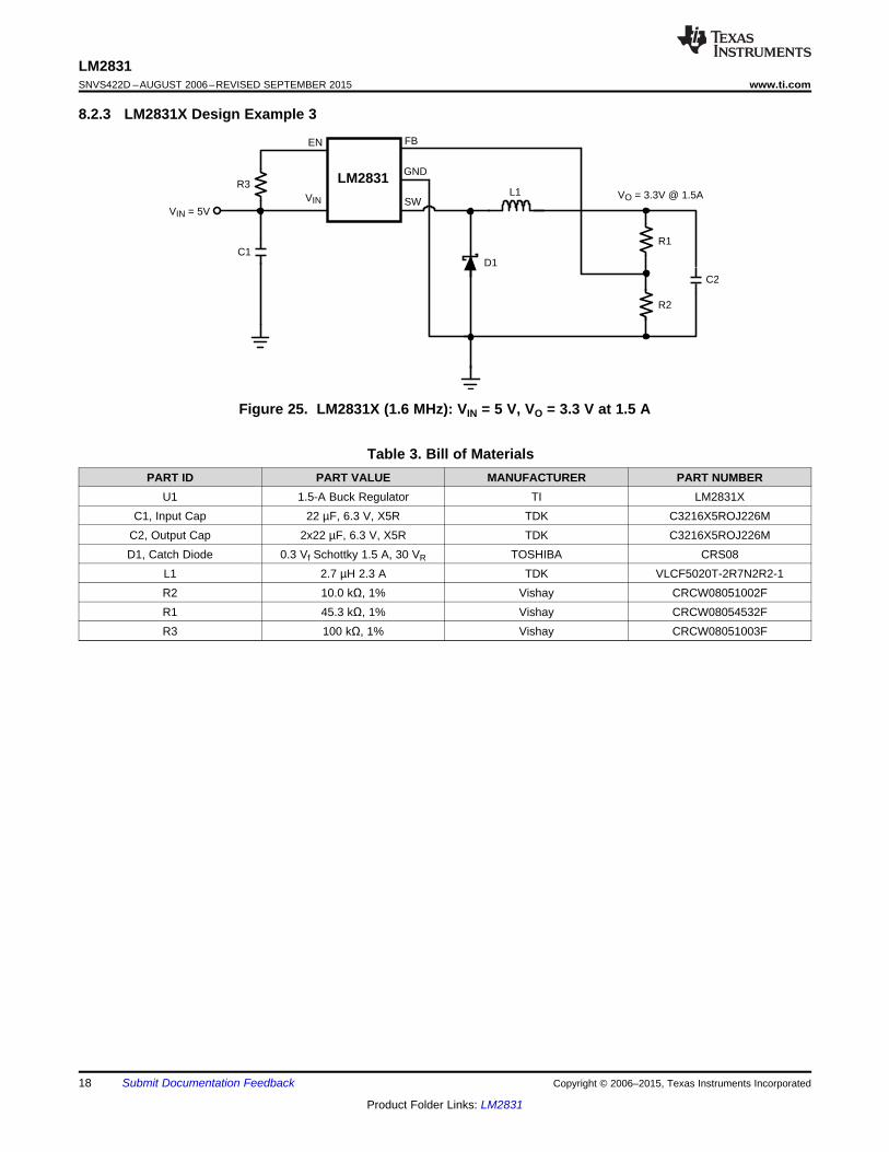
8.2.3 LM2831X Design Example 3
Figure 25. LM2831X (1.6 MHz): VIN = 5 V, VO = 3.3 V at 1.5 A
Table 3. Bill of MaterialsPART ID PART VALUE MANUFACTURER PART NUMBER
U1 1.5-A Buck Regulator TI LM2831XC1, Input Cap 22 µF, 6.3 V, X5R TDK C3216X5ROJ226M
C2, Output Cap 2x22 µF, 6.3 V, X5R TDK C3216X5ROJ226MD1, Catch Diode 0.3 Vf Schottky 1.5 A, 30 VR TOSHIBA CRS08
L1 2.7 µH 2.3 A TDK VLCF5020T-2R7N2R2-1R2 10.0 kΩ, 1% Vishay CRCW08051002FR1 45.3 kΩ, 1% Vishay CRCW08054532FR3 100 kΩ, 1% Vishay CRCW08051003F
18 Submit Documentation Feedback Copyright © 2006–2015, Texas Instruments Incorporated
Product Folder Links: LM2831

GND
FBEN
VIN SWVIN = 5V
C1
R3
D1
L1LM2831
R2
R1
C2
VO = 3.3V @ 1.5A
LM2831www.ti.com SNVS422D –AUGUST 2006–REVISED SEPTEMBER 2015
8.2.4 LM2831Y Design Example 4
Figure 26. LM2831Y (550 kHz): VIN = 5 V, VOUT = 3.3 V at 1.5 A
Table 4. Bill of MaterialsPART ID PART VALUE MANUFACTURER PART NUMBER
U1 1.5-A Buck Regulator TI LM2831YC1, Input Cap 22 µF, 6.3 V, X5R TDK C3216X5ROJ226M
C2, Output Cap 2x22 µF, 6.3 V, X5R TDK C3216X5ROJ226MD1, Catch Diode 0.3 Vf Schottky 1.5 A, 30 VR TOSHIBA CRS08
L1 4.7 µH 2.1 A TDK SLF7045T-4R7M2R0-PFR1 45.3 kΩ, 1% Vishay CRCW080545K3FKEAR2 10.0 kΩ, 1% Vishay CRCW08051002F
Copyright © 2006–2015, Texas Instruments Incorporated Submit Documentation Feedback 19
Product Folder Links: LM2831

GND
FBEN
VIN SWVIN = 5V
C1
R3
D1
L1LM2831
R2
R1
C2
VO = 1.2V @ 1.5A
LM2831SNVS422D –AUGUST 2006–REVISED SEPTEMBER 2015 www.ti.com
8.2.5 LM2831Y Design Example 5
Figure 27. LM2831Y (550 kHz): VIN = 5 V, VOUT = 1.2 V at 1.5 A
Table 5. Bill of MaterialsPART ID PART VALUE MANUFACTURER PART NUMBER
U1 1.5-A Buck Regulator TI LM2831YC1, Input Cap 22 µF, 6.3 V, X5R TDK C3216X5ROJ226M
C2, Output Cap 2x22 µF, 6.3 V, X5R TDK C3216X5ROJ226MD1, Catch Diode 0.3 Vf Schottky 1.5 A, 30 VR TOSHIBA CRS08
L1 6.8 µH 1.8 A TDK SLF7045T-6R8M1R7R1 10.0 kΩ, 1% Vishay CRCW08051002FR2 10.0 kΩ, 1% Vishay CRCW08051002F
20 Submit Documentation Feedback Copyright © 2006–2015, Texas Instruments Incorporated
Product Folder Links: LM2831

GND
FBEN
VIN SWVIN = 5V
C1
R3
D1
L1LM2831
R2
R1
C2
VO = 3.3V @ 1.5A
LM2831www.ti.com SNVS422D –AUGUST 2006–REVISED SEPTEMBER 2015
8.2.6 LM2831Z Design Example 6
Figure 28. LM2831Z (3 MHz): VIN = 5 V, VO = 3.3 V at 1.5 A
Table 6. Bill of MaterialsPART ID PART VALUE MANUFACTURER PART NUMBER
U1 1.5-A Buck Regulator TI LM2831ZC1, Input Cap 22 µF, 6.3 V, X5R TDK C3216X5ROJ226M
C2, Output Cap 2x22 µF, 6.3 V, X5R TDK C3216X5ROJ226MD1, Catch Diode 0.3 Vf Schottky 1.5 A, 30 VR TOSHIBA CRS08
L1 1.6 µH 2.0 A TDK VLCF4018T-1R6N1R7-2R2 10.0 kΩ, 1% Vishay CRCW08051002FR1 45.3 kΩ, 1% Vishay CRCW08054532FR3 100 kΩ, 1% Vishay CRCW08051003F
Copyright © 2006–2015, Texas Instruments Incorporated Submit Documentation Feedback 21
Product Folder Links: LM2831

GND
FBEN
VIN SWVIN = 5V
C1
R3
D1
L1LM2831
R2
R1
C2
VO = 1.2V @ 1.5A
LM2831SNVS422D –AUGUST 2006–REVISED SEPTEMBER 2015 www.ti.com
8.2.7 LM2831Z Design Example 7
Figure 29. LM2831Z (3 MHz): VIN = 5 V, VO = 1.2 V at 1.5 A
Table 7. Bill of MaterialsPART ID PART VALUE MANUFACTURER PART NUMBER
U1 1.5-A Buck Regulator TI LM2831ZC1, Input Cap 22 µF, 6.3 V, X5R TDK C3216X5ROJ226M
C2, Output Cap 2x22 µF, 6.3 V, X5R TDK C3216X5ROJ226MD1, Catch Diode 0.3 Vf Schottky 1.5 A, 30 VR TOSHIBA CRS08
L1 1.6 µH, 2.0 A TDK VLCF4018T- 1R6N1R7-2R2 10.0 kΩ, 1% Vishay CRCW08051002FR1 10.0 kΩ, 1% Vishay CRCW08051002FR3 100 kΩ, 1% Vishay CRCW08051003F
22 Submit Documentation Feedback Copyright © 2006–2015, Texas Instruments Incorporated
Product Folder Links: LM2831

LP3470M5X-3.08
U2
VINAVIND
LM2831
U3
U1
LM2831
SW
D1
FB
EN
L1
GND
C1
C2
R1
R2
C3 VINAVIND
SW
FB
EN
GND
D2
L2
C4
R4
R5
R6 3
1
2
VIN
RESET
4
5
LP3470
C7VIN
VO = 3.3V @ 1.5A
VO = 1.2V @ 1.5A
R3
LM2831www.ti.com SNVS422D –AUGUST 2006–REVISED SEPTEMBER 2015
8.2.8 LM2831X Dual Converters with Delayed Enabled Design Example 8
Figure 30. LM2831X (1.6 MHz): VIN = 5 V, VO = 1.2 V at 1.5 A and 3.3 V at1.5 A
Table 8. Bill of MaterialsPART ID PART VALUE MANUFACTURER PART NUMBERU1, U2 1.5-A Buck Regulator TI LM2831X
U3 Power on Reset TI LP3470M5X-3.08C1, C3 Input Cap 22 µF, 6.3 V, X5R TDK C3216X5ROJ226M
C2, C4 Output Cap 2x22 µF, 6.3 V, X5R TDK C3216X5ROJ226MC7 Trr delay capacitor TDK
D1, D2 Catch Diode 0.3 Vf Schottky 1.5 A, 30 VR TOSHIBA CRS08L1, L2 3.3 µH, 2.2 A TDK VLCF5020T-3R3N2R0-1
R2, R4, R5 10.0 kΩ, 1% Vishay CRCW08051002FR1, R6 45.3 kΩ, 1% Vishay CRCW08054532F
R3 100 kΩ, 1% Vishay CRCW08051003F
Copyright © 2006–2015, Texas Instruments Incorporated Submit Documentation Feedback 23
Product Folder Links: LM2831

LDO
C5
U2
D2
L2
R1
R2
EN FB
SW
VINA
VIND
GNDVO = 3.3V @ 1.5A
VO = 5.0V @ 150mA
C4
C6
C2
C3
D1
L1
U1
C1
LM2831VIN = 5V
LM2831SNVS422D –AUGUST 2006–REVISED SEPTEMBER 2015 www.ti.com
8.2.9 LM2831X Buck Converter and Voltage Double Circuit With LDO Follower Design Example 9
Figure 31. LM2831X (1.6 MHz): VIN = 5 V, VO = 3.3 V at 1.5 A and LP2986-5.0 at 150 mA
Table 9. Bill of MaterialsPART ID PART VALUE MANUFACTURER PART NUMBER
U1 1.5-A Buck Regulator TI LM2831XU2 200-mA LDO TI LP2986-5.0
C1, Input Cap 22 µF, 6.3 V, X5R TDK C3216X5ROJ226MC2, Output Cap 22 µF, 6.3 V, X5R TDK C3216X5ROJ226M
C3 – C6 2.2 µF, 6.3 V, X5R TDK C1608X5R0J225MD1, Catch Diode 0.3 Vf Schottky 1.5 A, 30 VR TOSHIBA CRS08
D2 0.4 Vf Schottky 20 VR, 500 mA ON Semi MBR0520L2 10 µH, 800 mA CoilCraft ME3220-103L1 3.3 µH, 2.2 A TDK VLCF5020T-3R3N2R0-1R2 45.3 kΩ, 1% Vishay CRCW08054532FR1 10.0 kΩ, 1% Vishay CRCW08051002F
24 Submit Documentation Feedback Copyright © 2006–2015, Texas Instruments Incorporated
Product Folder Links: LM2831

D =VOUT + VD + VDCR
VIN + VD + VDCR - VSW
OUT D
IN D SW
V VD
V V V
+
=
+ -
OUT
OUT LOSS
P
P Ph =
+
OUT
IN
P
Ph =
LM2831www.ti.com SNVS422D –AUGUST 2006–REVISED SEPTEMBER 2015
9 Power Supply RecommendationsThe LM2831 device is designed to operate from various DC power supplies. The impedance of the input supplyrail should be low enough that the input current transient does not cause a drop below the UVLO level. If theinput supply is connected by using long wires, additional bulk capacitance may be required in addition to normalinput capacitor.
10 Layout
10.1 Layout GuidelinesWhen planning layout there are a few things to consider when trying to achieve a clean, regulated output. Themost important consideration is the close coupling of the GND connections of the input capacitor and the catchdiode D1. These ground ends should be close to one another and be connected to the GND plane with at leasttwo through-holes. Place these components as close to the IC as possible. Next in importance is the location ofthe GND connection of the output capacitor, which should be near the GND connections of CIN and D1. Thereshould be a continuous ground plane on the bottom layer of a two-layer board except under the switching nodeisland. The FB pin is a high impedance node and care should be taken to make the FB trace short to avoid noisepickup and inaccurate regulation. The feedback resistors should be placed as close as possible to the IC, withthe GND of R1 placed as close as possible to the GND of the IC. The VOUT trace to R2 should be routed awayfrom the inductor and any other traces that are switching. High AC currents flow through the VIN, SW and VOUTtraces, so they should be as short and wide as possible. However, making the traces wide increases radiatednoise, so the designer must make this trade-off. Radiated noise can be decreased by choosing a shieldedinductor. The remaining components should also be placed as close as possible to the IC. See Application NoteAN-1229 SNVA054 for further considerations and the LM2831 demo board as an example of a 4-layer layout.
10.1.1 Calculating Efficiency and Junction TemperatureThe complete LM2831 DC-DC converter efficiency can be calculated in the following manner.
(15)
Or
(16)
Calculations for determining the most significant power losses are shown below. Other losses totaling less than2% are not discussed.
Power loss (PLOSS) is the sum of two basic types of losses in the converter: switching and conduction.Conduction losses usually dominate at higher output loads, whereas switching losses remain relatively fixed anddominate at lower output loads. The first step in determining the losses is to calculate the duty cycle (D):
(17)
VSW is the voltage drop across the internal PFET when it is on, and is equal to:VSW = IOUT × RDSON (18)
VD is the forward voltage drop across the Schottky catch diode. It can be obtained from the diode manufacturesElectrical Characteristics section. If the voltage drop across the inductor (VDCR) is accounted for, the equationbecomes:
(19)
The conduction losses in the free-wheeling Schottky diode are calculated as follows:PDIODE = VD × IOUT × (1-D) (20)
Copyright © 2006–2015, Texas Instruments Incorporated Submit Documentation Feedback 25
Product Folder Links: LM2831

PCOND= (IOUT2 x D)
13
1 + x'iLIOUT
2
RDSON
LM2831SNVS422D –AUGUST 2006–REVISED SEPTEMBER 2015 www.ti.com
Layout Guidelines (continued)Often this is the single most significant power loss in the circuit. Care should be taken to choose a Schottkydiode that has a low forward voltage drop.
Another significant external power loss is the conduction loss in the output inductor. The equation can besimplified to:
PIND = IOUT2 × RDCR (21)
The LM2831 conduction loss is mainly associated with the internal PFET:
(22)
If the inductor ripple current is fairly small, the conduction losses can be simplified to:PCOND = IOUT
2 × RDSON × D (23)
Switching losses are also associated with the internal PFET. They occur during the switch on and off transitionperiods, where voltages and currents overlap resulting in power loss. The simplest means to determine this lossis to empirically measuring the rise and fall times (10% to 90%) of the switch at the switch node.
Switching power loss is calculated as follows:PSWR = 1/2(VIN × IOUT × FSW × TRISE) (24)PSWF = 1/2(VIN × IOUT × FSW × TFALL) (25)PSW = PSWR + PSWF (26)
Another loss is the power required for operation of the internal circuitry:PQ = IQ × VIN (27)
IQ is the quiescent operating current, and is typically around 2.5 mA for the 0.55-MHz frequency option.
Typical application power losses are:
Table 10. Power Loss TabulationPARAMETER VALUE PARAMETER VALUE
VIN 5 VVOUT 3.3 V POUT 4.125 WIOUT 1.25 AVD 0.45 V PDIODE 188 mW
FSW 550 kHzIQ 2.5 mA PQ 12.5 mW
TRISE 4 nS PSWR 7 mWTFALL 4 nS PSWF 7 mW
RDS(ON) 150 mΩ PCOND 156 mWINDDCR 70 mΩ PIND 110 mW
D 0.667 PLOSS 481 mWη 88% PINTERNAL 183 mW
ΣPCOND + PSW + PDIODE + PIND + PQ = PLOSS (28)ΣPCOND + PSWF + PSWR + PQ = PINTERNAL (29)PINTERNAL = 183 mW (30)
26 Submit Documentation Feedback Copyright © 2006–2015, Texas Instruments Incorporated
Product Folder Links: LM2831

J CJC
T TR
PowerF
-=
J AJA
T TR
Powerq
-=
TR
Powerq
D=
LM2831www.ti.com SNVS422D –AUGUST 2006–REVISED SEPTEMBER 2015
10.1.2 Thermal DefinitionsTJ Chip junction temperature
TA Ambient temperature
RθJC Thermal resistance from chip junction to device case
RθJA Thermal resistance from chip junction to ambient air
Heat in the LM2831 due to internal power dissipation is removed through conduction and/or convection.
Conduction Heat transfer occurs through cross sectional areas of material. Depending on the material, thetransfer of heat can be considered to have poor to good thermal conductivity properties (insulatorvs. conductor).
Heat Transfer goes as:
Silicon → package → lead frame → PCB
Convection: Heat transfer is by means of airflow. This could be from a fan or natural convection. Naturalconvection occurs when air currents rise from the hot device to cooler air.
Thermal impedance is defined as:
(31)
Thermal impedance from the silicon junction to the ambient air is defined as:
(32)
The PCB size, weight of copper used to route traces and ground plane, and number of layers within the PCB cangreatly effect RθJA. The type and number of thermal vias can also make a large difference in the thermalimpedance. Thermal vias are necessary in most applications. They conduct heat from the surface of the PCB tothe ground plane. Four to six thermal vias should be placed under the exposed pad to the ground plane if theWSON package is used.
Thermal impedance also depends on the thermal properties of the application operating conditions (Vin, Vo, Io,and so forth), and the surrounding circuitry.
10.1.2.1 Silicon Junction Temperature Determination Method 1To accurately measure the silicon temperature for a given application, two methods can be used. The firstmethod requires the user to know the thermal impedance of the silicon junction to top case temperature.
Some clarification must be made before we go any further.
RθJC is the thermal impedance from all six sides of an IC package to silicon junction.
RΦJC is the thermal impedance from top case to the silicon junction.
In this data sheet we will use RΦJC so that it allows the user to measure top case temperature with a smallthermocouple attached to the top case.
RΦJC is approximately 30°C/Watt for the 6-pin WSON package with the exposed pad. Knowing the internaldissipation from the efficiency calculation given previously, and the case temperature, which can be empiricallymeasured on the bench we have:
(33)
Therefore:Tj = (RΦJC × PLOSS) + TC (34)
From the previous example:Tj = (RΦJC × PINTERNAL) + TC (35)Tj = 30°C/W × 0.189 W + TC (36)
Copyright © 2006–2015, Texas Instruments Incorporated Submit Documentation Feedback 27
Product Folder Links: LM2831

Die AttachMaterial
Mold Compound
Gold Wire
Exposed DieAttach Pad
Die
Cu
ExposedContact
JA
165 C 144 CR 111 C / W
189 mWq
° - °= = °
JA
INTERNAL
165 C TaR
Pq
° -=
LM2831SNVS422D –AUGUST 2006–REVISED SEPTEMBER 2015 www.ti.com
The second method can give a very accurate silicon junction temperature.
The first step is to determine RθJA of the application. The LM2831 has overtemperature protection circuitry. Whenthe silicon temperature reaches 165°C, the device stops switching. The protection circuitry has a hysteresis ofabout 15°C. Once the silicon temperature has decreased to approximately 150°C, the device will start to switchagain. Knowing this, the RθJA for any application can be characterized during the early stages of the design onemay calculate the RθJA by placing the PCB circuit into a thermal chamber. Raise the ambient temperature in thegiven working application until the circuit enters thermal shutdown. If the SW-pin is monitored, it will be obviouswhen the internal PFET stops switching, indicating a junction temperature of 165°C. Knowing the internal powerdissipation from the above methods, the junction temperature, and the ambient temperature RθJA can bedetermined.
(37)
Once this is determined, the maximum ambient temperature allowed for a desired junction temperature can befound.
An example of calculating RθJA for an application using the Texas Instruments LM2831 WSON demonstrationboard is shown below.
The four layer PCB is constructed using FR4 with ½ oz copper traces. The copper ground plane is on the bottomlayer. The ground plane is accessed by two vias. The board measures 3 cm × 3 cm. It was placed in an ovenwith no forced airflow. The ambient temperature was raised to 144°C, and at that temperature, the device wentinto thermal shutdown.
From the previous example:PINTERNAL = 189 mW (38)
(39)
If the junction temperature was to be kept below 125°C, then the ambient temperature could not go above 109°CTj - (RθJA × PLOSS) = TA (40)125°C - (111°C/W × 189 mW) = 104°C (41)
10.1.3 WSON Package
Figure 32. Internal WSON Connection
For certain high power applications, the PCB land may be modified to a "dog bone" shape (see Figure 33). Byincreasing the size of ground plane, and adding thermal vias, the RθJA for the application can be reduced.
28 Submit Documentation Feedback Copyright © 2006–2015, Texas Instruments Incorporated
Product Folder Links: LM2831

1
2
4
6
5
ENFB
SW
VINA
VIND
GND GND
PLANE
3
LM2831www.ti.com SNVS422D –AUGUST 2006–REVISED SEPTEMBER 2015
10.2 Layout Example
Figure 33. 6-Lead WSON PCB Dog Bone Layout
Copyright © 2006–2015, Texas Instruments Incorporated Submit Documentation Feedback 29
Product Folder Links: LM2831

LM2831SNVS422D –AUGUST 2006–REVISED SEPTEMBER 2015 www.ti.com
11 Device and Documentation Support
11.1 Device Support
11.1.1 Third-Party Products DisclaimerTI'S PUBLICATION OF INFORMATION REGARDING THIRD-PARTY PRODUCTS OR SERVICES DOES NOTCONSTITUTE AN ENDORSEMENT REGARDING THE SUITABILITY OF SUCH PRODUCTS OR SERVICESOR A WARRANTY, REPRESENTATION OR ENDORSEMENT OF SUCH PRODUCTS OR SERVICES, EITHERALONE OR IN COMBINATION WITH ANY TI PRODUCT OR SERVICE.
11.2 Documentation Support
11.2.1 Related DocumentationFor related documentation, see the following:
AN-1229 SIMPLE SWITCHER ® PCB Layout Guidelines, SNVA054
11.3 Community ResourcesThe following links connect to TI community resources. Linked contents are provided "AS IS" by the respectivecontributors. They do not constitute TI specifications and do not necessarily reflect TI's views; see TI's Terms ofUse.
TI E2E™ Online Community TI's Engineer-to-Engineer (E2E) Community. Created to foster collaborationamong engineers. At e2e.ti.com, you can ask questions, share knowledge, explore ideas and helpsolve problems with fellow engineers.
Design Support TI's Design Support Quickly find helpful E2E forums along with design support tools andcontact information for technical support.
11.4 TrademarksE2E is a trademark of Texas Instruments.All other trademarks are the property of their respective owners.
11.5 Electrostatic Discharge CautionThese devices have limited built-in ESD protection. The leads should be shorted together or the device placed in conductive foamduring storage or handling to prevent electrostatic damage to the MOS gates.
11.6 GlossarySLYZ022 — TI Glossary.
This glossary lists and explains terms, acronyms, and definitions.
12 Mechanical, Packaging, and Orderable InformationThe following pages include mechanical, packaging, and orderable information. This information is the mostcurrent data available for the designated devices. This data is subject to change without notice and revision ofthis document. For browser-based versions of this data sheet, refer to the left-hand navigation.
30 Submit Documentation Feedback Copyright © 2006–2015, Texas Instruments Incorporated
Product Folder Links: LM2831

PACKAGE OPTION ADDENDUM
www.ti.com 8-Oct-2015
Addendum-Page 1
PACKAGING INFORMATION
Orderable Device Status(1)
Package Type PackageDrawing
Pins PackageQty
Eco Plan(2)
Lead/Ball Finish(6)
MSL Peak Temp(3)
Op Temp (°C) Device Marking(4/5)
Samples
LM2831XMF/NOPB ACTIVE SOT-23 DBV 5 1000 Green (RoHS& no Sb/Br)
CU SN Level-1-260C-UNLIM -40 to 125 SKYB
LM2831XMFX/NOPB ACTIVE SOT-23 DBV 5 3000 Green (RoHS& no Sb/Br)
CU SN Level-1-260C-UNLIM -40 to 125 SKYB
LM2831XSD NRND WSON NGG 6 1000 TBD Call TI Call TI -40 to 125 L193B
LM2831XSD/NOPB ACTIVE WSON NGG 6 1000 Green (RoHS& no Sb/Br)
CU SN Level-3-260C-168 HR -40 to 125 L193B
LM2831XSDX/NOPB ACTIVE WSON NGG 6 4500 Green (RoHS& no Sb/Br)
CU SN Level-3-260C-168 HR -40 to 125 L193B
LM2831YMF/NOPB ACTIVE SOT-23 DBV 5 1000 Green (RoHS& no Sb/Br)
CU SN Level-1-260C-UNLIM -40 to 125 SKZB
LM2831YMFX/NOPB ACTIVE SOT-23 DBV 5 3000 Green (RoHS& no Sb/Br)
CU SN Level-1-260C-UNLIM -40 to 125 SKZB
LM2831YSD/NOPB ACTIVE WSON NGG 6 1000 Green (RoHS& no Sb/Br)
CU SN Level-3-260C-168 HR -40 to 125 L194B
LM2831ZMF/NOPB ACTIVE SOT-23 DBV 5 1000 Green (RoHS& no Sb/Br)
CU SN Level-1-260C-UNLIM -40 to 125 SLAB
LM2831ZSD/NOPB ACTIVE WSON NGG 6 1000 Green (RoHS& no Sb/Br)
CU SN Level-3-260C-168 HR -40 to 125 L195B
(1) The marketing status values are defined as follows:ACTIVE: Product device recommended for new designs.LIFEBUY: TI has announced that the device will be discontinued, and a lifetime-buy period is in effect.NRND: Not recommended for new designs. Device is in production to support existing customers, but TI does not recommend using this part in a new design.PREVIEW: Device has been announced but is not in production. Samples may or may not be available.OBSOLETE: TI has discontinued the production of the device.
(2) Eco Plan - The planned eco-friendly classification: Pb-Free (RoHS), Pb-Free (RoHS Exempt), or Green (RoHS & no Sb/Br) - please check http://www.ti.com/productcontent for the latest availabilityinformation and additional product content details.TBD: The Pb-Free/Green conversion plan has not been defined.Pb-Free (RoHS): TI's terms "Lead-Free" or "Pb-Free" mean semiconductor products that are compatible with the current RoHS requirements for all 6 substances, including the requirement thatlead not exceed 0.1% by weight in homogeneous materials. Where designed to be soldered at high temperatures, TI Pb-Free products are suitable for use in specified lead-free processes.Pb-Free (RoHS Exempt): This component has a RoHS exemption for either 1) lead-based flip-chip solder bumps used between the die and package, or 2) lead-based die adhesive used betweenthe die and leadframe. The component is otherwise considered Pb-Free (RoHS compatible) as defined above.Green (RoHS & no Sb/Br): TI defines "Green" to mean Pb-Free (RoHS compatible), and free of Bromine (Br) and Antimony (Sb) based flame retardants (Br or Sb do not exceed 0.1% by weightin homogeneous material)

PACKAGE OPTION ADDENDUM
www.ti.com 8-Oct-2015
Addendum-Page 2
(3) MSL, Peak Temp. - The Moisture Sensitivity Level rating according to the JEDEC industry standard classifications, and peak solder temperature.
(4) There may be additional marking, which relates to the logo, the lot trace code information, or the environmental category on the device.
(5) Multiple Device Markings will be inside parentheses. Only one Device Marking contained in parentheses and separated by a "~" will appear on a device. If a line is indented then it is a continuationof the previous line and the two combined represent the entire Device Marking for that device.
(6) Lead/Ball Finish - Orderable Devices may have multiple material finish options. Finish options are separated by a vertical ruled line. Lead/Ball Finish values may wrap to two lines if the finishvalue exceeds the maximum column width.
Important Information and Disclaimer:The information provided on this page represents TI's knowledge and belief as of the date that it is provided. TI bases its knowledge and belief on informationprovided by third parties, and makes no representation or warranty as to the accuracy of such information. Efforts are underway to better integrate information from third parties. TI has taken andcontinues to take reasonable steps to provide representative and accurate information but may not have conducted destructive testing or chemical analysis on incoming materials and chemicals.TI and TI suppliers consider certain information to be proprietary, and thus CAS numbers and other limited information may not be available for release.
In no event shall TI's liability arising out of such information exceed the total purchase price of the TI part(s) at issue in this document sold by TI to Customer on an annual basis.

TAPE AND REEL INFORMATION
*All dimensions are nominal
Device PackageType
PackageDrawing
Pins SPQ ReelDiameter
(mm)
ReelWidth
W1 (mm)
A0(mm)
B0(mm)
K0(mm)
P1(mm)
W(mm)
Pin1Quadrant
LM2831XMF/NOPB SOT-23 DBV 5 1000 178.0 8.4 3.2 3.2 1.4 4.0 8.0 Q3
LM2831XMFX/NOPB SOT-23 DBV 5 3000 178.0 8.4 3.2 3.2 1.4 4.0 8.0 Q3
LM2831XSD WSON NGG 6 1000 178.0 12.4 3.3 3.3 1.0 8.0 12.0 Q1
LM2831XSD/NOPB WSON NGG 6 1000 178.0 12.4 3.3 3.3 1.0 8.0 12.0 Q1
LM2831XSDX/NOPB WSON NGG 6 4500 330.0 12.4 3.3 3.3 1.0 8.0 12.0 Q1
LM2831YMF/NOPB SOT-23 DBV 5 1000 178.0 8.4 3.2 3.2 1.4 4.0 8.0 Q3
LM2831YMFX/NOPB SOT-23 DBV 5 3000 178.0 8.4 3.2 3.2 1.4 4.0 8.0 Q3
LM2831YSD/NOPB WSON NGG 6 1000 178.0 12.4 3.3 3.3 1.0 8.0 12.0 Q1
LM2831ZMF/NOPB SOT-23 DBV 5 1000 178.0 8.4 3.2 3.2 1.4 4.0 8.0 Q3
LM2831ZSD/NOPB WSON NGG 6 1000 178.0 12.4 3.3 3.3 1.0 8.0 12.0 Q1
PACKAGE MATERIALS INFORMATION
www.ti.com 20-Dec-2016
Pack Materials-Page 1

*All dimensions are nominal
Device Package Type Package Drawing Pins SPQ Length (mm) Width (mm) Height (mm)
LM2831XMF/NOPB SOT-23 DBV 5 1000 210.0 185.0 35.0
LM2831XMFX/NOPB SOT-23 DBV 5 3000 210.0 185.0 35.0
LM2831XSD WSON NGG 6 1000 210.0 185.0 35.0
LM2831XSD/NOPB WSON NGG 6 1000 210.0 185.0 35.0
LM2831XSDX/NOPB WSON NGG 6 4500 367.0 367.0 35.0
LM2831YMF/NOPB SOT-23 DBV 5 1000 210.0 185.0 35.0
LM2831YMFX/NOPB SOT-23 DBV 5 3000 210.0 185.0 35.0
LM2831YSD/NOPB WSON NGG 6 1000 210.0 185.0 35.0
LM2831ZMF/NOPB SOT-23 DBV 5 1000 210.0 185.0 35.0
LM2831ZSD/NOPB WSON NGG 6 1000 210.0 185.0 35.0
PACKAGE MATERIALS INFORMATION
www.ti.com 20-Dec-2016
Pack Materials-Page 2


www.ti.com
PACKAGE OUTLINE
C
TYP0.220.08
0.25
3.02.6
2X 0.95
1.9
1.45 MAX
TYP0.150.00
5X 0.50.3
TYP0.60.3
TYP80
1.9
A
3.052.75
B1.751.45
(1.1)
SOT-23 - 1.45 mm max heightDBV0005ASMALL OUTLINE TRANSISTOR
4214839/C 04/2017
NOTES: 1. All linear dimensions are in millimeters. Any dimensions in parenthesis are for reference only. Dimensioning and tolerancing per ASME Y14.5M.2. This drawing is subject to change without notice.3. Refernce JEDEC MO-178.
0.2 C A B
1
34
5
2
INDEX AREAPIN 1
GAGE PLANE
SEATING PLANE
0.1 C
SCALE 4.000
www.ti.com
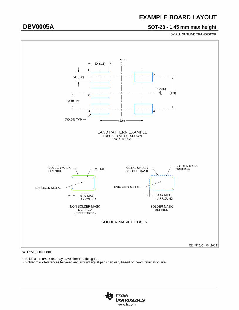
EXAMPLE BOARD LAYOUT
0.07 MAXARROUND
0.07 MINARROUND
5X (1.1)
5X (0.6)
(2.6)
(1.9)
2X (0.95)
(R0.05) TYP
4214839/C 04/2017
SOT-23 - 1.45 mm max heightDBV0005ASMALL OUTLINE TRANSISTOR
NOTES: (continued) 4. Publication IPC-7351 may have alternate designs. 5. Solder mask tolerances between and around signal pads can vary based on board fabrication site.
SYMM
LAND PATTERN EXAMPLEEXPOSED METAL SHOWN
SCALE:15X
PKG
1
3 4
5
2
SOLDER MASKOPENINGMETAL UNDER
SOLDER MASK
SOLDER MASKDEFINED
EXPOSED METAL
METALSOLDER MASKOPENING
NON SOLDER MASKDEFINED
(PREFERRED)
SOLDER MASK DETAILS
EXPOSED METAL

www.ti.com
EXAMPLE STENCIL DESIGN
(2.6)
(1.9)
2X(0.95)
5X (1.1)
5X (0.6)
(R0.05) TYP
SOT-23 - 1.45 mm max heightDBV0005ASMALL OUTLINE TRANSISTOR
4214839/C 04/2017
NOTES: (continued) 6. Laser cutting apertures with trapezoidal walls and rounded corners may offer better paste release. IPC-7525 may have alternate design recommendations. 7. Board assembly site may have different recommendations for stencil design.
SOLDER PASTE EXAMPLEBASED ON 0.125 mm THICK STENCIL
SCALE:15X
SYMM
PKG
1
3 4
5
2

MECHANICAL DATA
NGG0006A
www.ti.com
SDE06A (Rev A)

IMPORTANT NOTICE
Texas Instruments Incorporated (TI) reserves the right to make corrections, enhancements, improvements and other changes to itssemiconductor products and services per JESD46, latest issue, and to discontinue any product or service per JESD48, latest issue. Buyersshould obtain the latest relevant information before placing orders and should verify that such information is current and complete.TI’s published terms of sale for semiconductor products (http://www.ti.com/sc/docs/stdterms.htm) apply to the sale of packaged integratedcircuit products that TI has qualified and released to market. Additional terms may apply to the use or sale of other types of TI products andservices.Reproduction of significant portions of TI information in TI data sheets is permissible only if reproduction is without alteration and isaccompanied by all associated warranties, conditions, limitations, and notices. TI is not responsible or liable for such reproduceddocumentation. Information of third parties may be subject to additional restrictions. Resale of TI products or services with statementsdifferent from or beyond the parameters stated by TI for that product or service voids all express and any implied warranties for theassociated TI product or service and is an unfair and deceptive business practice. TI is not responsible or liable for any such statements.Buyers and others who are developing systems that incorporate TI products (collectively, “Designers”) understand and agree that Designersremain responsible for using their independent analysis, evaluation and judgment in designing their applications and that Designers havefull and exclusive responsibility to assure the safety of Designers' applications and compliance of their applications (and of all TI productsused in or for Designers’ applications) with all applicable regulations, laws and other applicable requirements. Designer represents that, withrespect to their applications, Designer has all the necessary expertise to create and implement safeguards that (1) anticipate dangerousconsequences of failures, (2) monitor failures and their consequences, and (3) lessen the likelihood of failures that might cause harm andtake appropriate actions. Designer agrees that prior to using or distributing any applications that include TI products, Designer willthoroughly test such applications and the functionality of such TI products as used in such applications.TI’s provision of technical, application or other design advice, quality characterization, reliability data or other services or information,including, but not limited to, reference designs and materials relating to evaluation modules, (collectively, “TI Resources”) are intended toassist designers who are developing applications that incorporate TI products; by downloading, accessing or using TI Resources in anyway, Designer (individually or, if Designer is acting on behalf of a company, Designer’s company) agrees to use any particular TI Resourcesolely for this purpose and subject to the terms of this Notice.TI’s provision of TI Resources does not expand or otherwise alter TI’s applicable published warranties or warranty disclaimers for TIproducts, and no additional obligations or liabilities arise from TI providing such TI Resources. TI reserves the right to make corrections,enhancements, improvements and other changes to its TI Resources. TI has not conducted any testing other than that specificallydescribed in the published documentation for a particular TI Resource.Designer is authorized to use, copy and modify any individual TI Resource only in connection with the development of applications thatinclude the TI product(s) identified in such TI Resource. NO OTHER LICENSE, EXPRESS OR IMPLIED, BY ESTOPPEL OR OTHERWISETO ANY OTHER TI INTELLECTUAL PROPERTY RIGHT, AND NO LICENSE TO ANY TECHNOLOGY OR INTELLECTUAL PROPERTYRIGHT OF TI OR ANY THIRD PARTY IS GRANTED HEREIN, including but not limited to any patent right, copyright, mask work right, orother intellectual property right relating to any combination, machine, or process in which TI products or services are used. Informationregarding or referencing third-party products or services does not constitute a license to use such products or services, or a warranty orendorsement thereof. Use of TI Resources may require a license from a third party under the patents or other intellectual property of thethird party, or a license from TI under the patents or other intellectual property of TI.TI RESOURCES ARE PROVIDED “AS IS” AND WITH ALL FAULTS. TI DISCLAIMS ALL OTHER WARRANTIES ORREPRESENTATIONS, EXPRESS OR IMPLIED, REGARDING RESOURCES OR USE THEREOF, INCLUDING BUT NOT LIMITED TOACCURACY OR COMPLETENESS, TITLE, ANY EPIDEMIC FAILURE WARRANTY AND ANY IMPLIED WARRANTIES OFMERCHANTABILITY, FITNESS FOR A PARTICULAR PURPOSE, AND NON-INFRINGEMENT OF ANY THIRD PARTY INTELLECTUALPROPERTY RIGHTS. TI SHALL NOT BE LIABLE FOR AND SHALL NOT DEFEND OR INDEMNIFY DESIGNER AGAINST ANY CLAIM,INCLUDING BUT NOT LIMITED TO ANY INFRINGEMENT CLAIM THAT RELATES TO OR IS BASED ON ANY COMBINATION OFPRODUCTS EVEN IF DESCRIBED IN TI RESOURCES OR OTHERWISE. IN NO EVENT SHALL TI BE LIABLE FOR ANY ACTUAL,DIRECT, SPECIAL, COLLATERAL, INDIRECT, PUNITIVE, INCIDENTAL, CONSEQUENTIAL OR EXEMPLARY DAMAGES INCONNECTION WITH OR ARISING OUT OF TI RESOURCES OR USE THEREOF, AND REGARDLESS OF WHETHER TI HAS BEENADVISED OF THE POSSIBILITY OF SUCH DAMAGES.Unless TI has explicitly designated an individual product as meeting the requirements of a particular industry standard (e.g., ISO/TS 16949and ISO 26262), TI is not responsible for any failure to meet such industry standard requirements.Where TI specifically promotes products as facilitating functional safety or as compliant with industry functional safety standards, suchproducts are intended to help enable customers to design and create their own applications that meet applicable functional safety standardsand requirements. Using products in an application does not by itself establish any safety features in the application. Designers mustensure compliance with safety-related requirements and standards applicable to their applications. Designer may not use any TI products inlife-critical medical equipment unless authorized officers of the parties have executed a special contract specifically governing such use.Life-critical medical equipment is medical equipment where failure of such equipment would cause serious bodily injury or death (e.g., lifesupport, pacemakers, defibrillators, heart pumps, neurostimulators, and implantables). Such equipment includes, without limitation, allmedical devices identified by the U.S. Food and Drug Administration as Class III devices and equivalent classifications outside the U.S.TI may expressly designate certain products as completing a particular qualification (e.g., Q100, Military Grade, or Enhanced Product).Designers agree that it has the necessary expertise to select the product with the appropriate qualification designation for their applicationsand that proper product selection is at Designers’ own risk. Designers are solely responsible for compliance with all legal and regulatoryrequirements in connection with such selection.Designer will fully indemnify TI and its representatives against any damages, costs, losses, and/or liabilities arising out of Designer’s non-compliance with the terms and provisions of this Notice.
Mailing Address: Texas Instruments, Post Office Box 655303, Dallas, Texas 75265Copyright © 2018, Texas Instruments Incorporated