lm35 precision centigrade temperature sensors - scrpdf.com monitoring... · lm35 to-can (3) 4.699...
TRANSCRIPT
LM35
+VS
R1
VOUT
tVS
LM35
+VS
(4 V to 20 V)
OUTPUT
0 mV + 10.0 mV/°C
Product
Folder
Sample &Buy
Technical
Documents
Tools &
Software
Support &Community
An IMPORTANT NOTICE at the end of this data sheet addresses availability, warranty, changes, use in safety-critical applications,intellectual property matters and other important disclaimers. PRODUCTION DATA.
LM35SNIS159G –AUGUST 1999–REVISED AUGUST 2016
LM35 Precision Centigrade Temperature Sensors
1
1 Features1• Calibrated Directly in Celsius (Centigrade)• Linear + 10-mV/°C Scale Factor• 0.5°C Ensured Accuracy (at 25°C)• Rated for Full −55°C to 150°C Range• Suitable for Remote Applications• Low-Cost Due to Wafer-Level Trimming• Operates from 4 V to 30 V• Less than 60-μA Current Drain• Low Self-Heating, 0.08°C in Still Air• Non-Linearity Only ±¼°C Typical• Low-Impedance Output, 0.1 Ω for 1-mA Load
2 Applications• Power Supplies• Battery Management• HVAC• Appliances
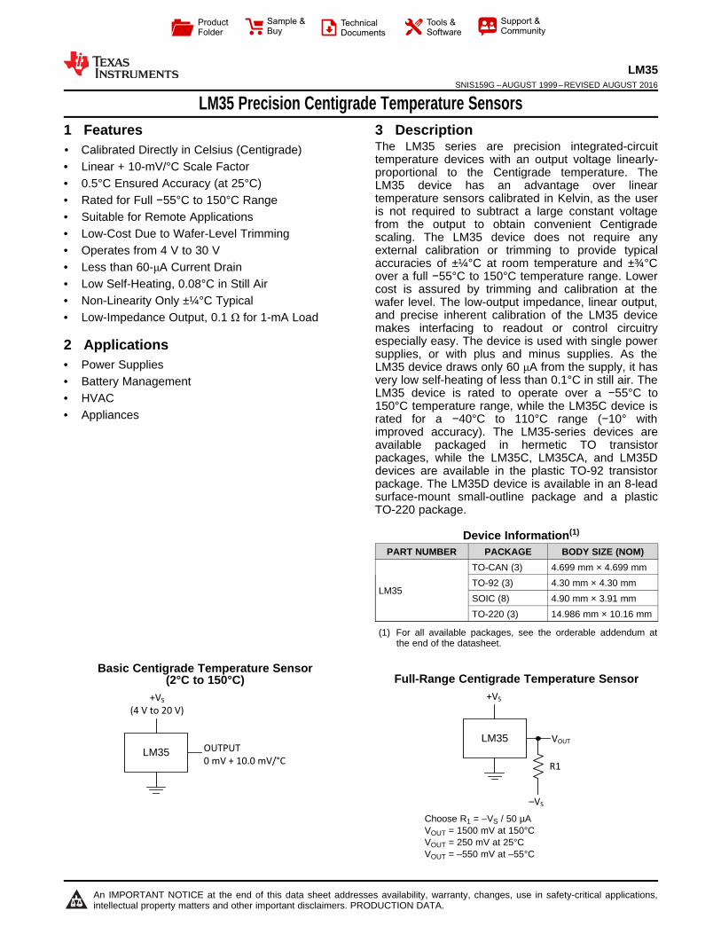
3 DescriptionThe LM35 series are precision integrated-circuittemperature devices with an output voltage linearly-proportional to the Centigrade temperature. TheLM35 device has an advantage over lineartemperature sensors calibrated in Kelvin, as the useris not required to subtract a large constant voltagefrom the output to obtain convenient Centigradescaling. The LM35 device does not require anyexternal calibration or trimming to provide typicalaccuracies of ±¼°C at room temperature and ±¾°Cover a full −55°C to 150°C temperature range. Lowercost is assured by trimming and calibration at thewafer level. The low-output impedance, linear output,and precise inherent calibration of the LM35 devicemakes interfacing to readout or control circuitryespecially easy. The device is used with single powersupplies, or with plus and minus supplies. As theLM35 device draws only 60 μA from the supply, it hasvery low self-heating of less than 0.1°C in still air. TheLM35 device is rated to operate over a −55°C to150°C temperature range, while the LM35C device israted for a −40°C to 110°C range (−10° withimproved accuracy). The LM35-series devices areavailable packaged in hermetic TO transistorpackages, while the LM35C, LM35CA, and LM35Ddevices are available in the plastic TO-92 transistorpackage. The LM35D device is available in an 8-leadsurface-mount small-outline package and a plasticTO-220 package.
Device Information(1)
PART NUMBER PACKAGE BODY SIZE (NOM)
LM35
TO-CAN (3) 4.699 mm × 4.699 mmTO-92 (3) 4.30 mm × 4.30 mmSOIC (8) 4.90 mm × 3.91 mmTO-220 (3) 14.986 mm × 10.16 mm
(1) For all available packages, see the orderable addendum atthe end of the datasheet.
Basic Centigrade Temperature Sensor(2°C to 150°C) Full-Range Centigrade Temperature Sensor
Choose R1 = –VS / 50 µAVOUT = 1500 mV at 150°CVOUT = 250 mV at 25°CVOUT = –550 mV at –55°C

2
LM35SNIS159G –AUGUST 1999–REVISED AUGUST 2016 www.ti.com
Product Folder Links: LM35
Submit Documentation Feedback Copyright © 1999–2016, Texas Instruments Incorporated
Table of Contents1 Features .................................................................. 12 Applications ........................................................... 13 Description ............................................................. 14 Revision History..................................................... 25 Pin Configuration and Functions ......................... 36 Specifications......................................................... 4
6.1 Absolute Maximum Ratings ...................................... 46.2 ESD Ratings.............................................................. 46.3 Recommended Operating Conditions....................... 46.4 Thermal Information .................................................. 46.5 Electrical Characteristics: LM35A, LM35CA Limits... 56.6 Electrical Characteristics: LM35A, LM35CA ............. 66.7 Electrical Characteristics: LM35, LM35C, LM35D
Limits.......................................................................... 86.8 Electrical Characteristics: LM35, LM35C, LM35D ... 96.9 Typical Characteristics ............................................ 11
7 Detailed Description ............................................ 137.1 Overview ................................................................. 137.2 Functional Block Diagram ....................................... 13
7.3 Feature Description................................................. 137.4 Device Functional Modes........................................ 13
8 Application and Implementation ........................ 148.1 Application Information............................................ 148.2 Typical Application .................................................. 158.3 System Examples ................................................... 16
9 Power Supply Recommendations ...................... 1910 Layout................................................................... 19
10.1 Layout Guidelines ................................................. 1910.2 Layout Example .................................................... 20
11 Device and Documentation Support ................. 2111.1 Receiving Notification of Documentation Updates 2111.2 Community Resources.......................................... 2111.3 Trademarks ........................................................... 2111.4 Electrostatic Discharge Caution............................ 2111.5 Glossary ................................................................ 21
12 Mechanical, Packaging, and OrderableInformation ........................................................... 21
4 Revision History
Changes from Revision F (January 2016) to Revision G Page
• Equation 1, changed From: 10 mV/°F To: 10mv/°C ............................................................................................................ 13• Power Supply Recommendations, changed From: "4-V to 5.5-V power supply" To: "4-V to 30-V power supply: .............. 19
Changes from Revision E (January 2015) to Revision F Page
• Changed NDV Package (TO-CAN) pinout from Top View to Bottom View ........................................................................... 3
Changes from Revision D (October 2013) to Revision E Page
• Added Pin Configuration and Functions section, ESD Ratings table, Feature Description section, Device FunctionalModes, Application and Implementation section, Power Supply Recommendations section, Layout section, Deviceand Documentation Support section, and Mechanical, Packaging, and Orderable Information section .............................. 1
Changes from Revision C (July 2013) to Revision D Page
• Changed W to Ω .................................................................................................................................................................... 1• Changed W to Ω in Abs Max tablenote. ................................................................................................................................ 4

+VS VOUT GND
+VSVOUT
GND
N.C.
N.C.
N.C.
N.C.
N.C.
12
3
4
87
6
5
+VS VOUT
GND
LM35DT
+VS VOUT
GND t
3
LM35www.ti.com SNIS159G –AUGUST 1999–REVISED AUGUST 2016
Product Folder Links: LM35
Submit Documentation FeedbackCopyright © 1999–2016, Texas Instruments Incorporated
5 Pin Configuration and Functions
NDV Package3-Pin TO-CAN(Bottom View)
Case is connected to negative pin (GND)
D Package8-PIN SOIC(Top View)
N.C. = No connection
LP Package3-Pin TO-92
(Bottom View)
NEB Package3-Pin TO-220(Top View)
Tab is connected to the negative pin(GND).NOTE: The LM35DT pinout is different thanthe discontinued LM35DP
Pin FunctionsPIN
TYPE DESCRIPTIONNAME TO46 TO92 TO220 SO8VOUT — — — 1 O Temperature Sensor Analog Output
N.C.— — — 2
— No Connection— — — 3
GND — — — 4 GROUND Device ground pin, connect to power supply negativeterminal
N.C.— — — 5
— No Connection— — — 6— — — 7
+VS — — — 8 POWER Positive power supply pin
4
LM35SNIS159G –AUGUST 1999–REVISED AUGUST 2016 www.ti.com
Product Folder Links: LM35
Submit Documentation Feedback Copyright © 1999–2016, Texas Instruments Incorporated
(1) If Military/Aerospace specified devices are required, please contact the Texas Instruments Sales Office/ Distributors for availability andspecifications.
(2) Absolute Maximum Ratings indicate limits beyond which damage to the device may occur. DC and AC electrical specifications do notapply when operating the device beyond its rated operating conditions.
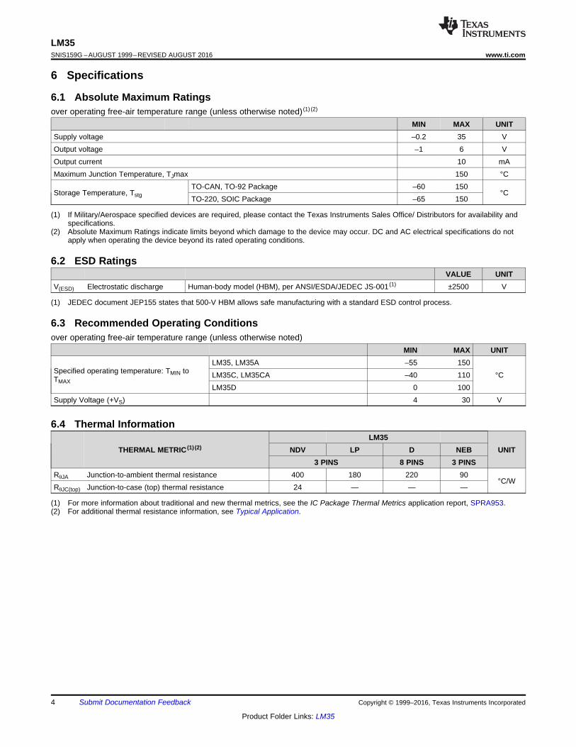
6 Specifications
6.1 Absolute Maximum Ratingsover operating free-air temperature range (unless otherwise noted) (1) (2)
MIN MAX UNITSupply voltage –0.2 35 VOutput voltage –1 6 VOutput current 10 mAMaximum Junction Temperature, TJmax 150 °C
Storage Temperature, TstgTO-CAN, TO-92 Package –60 150
°CTO-220, SOIC Package –65 150
(1) JEDEC document JEP155 states that 500-V HBM allows safe manufacturing with a standard ESD control process.
6.2 ESD RatingsVALUE UNIT
V(ESD) Electrostatic discharge Human-body model (HBM), per ANSI/ESDA/JEDEC JS-001 (1) ±2500 V
6.3 Recommended Operating Conditionsover operating free-air temperature range (unless otherwise noted)
MIN MAX UNIT
Specified operating temperature: TMIN toTMAX
LM35, LM35A –55 150°CLM35C, LM35CA –40 110
LM35D 0 100Supply Voltage (+VS) 4 30 V
(1) For more information about traditional and new thermal metrics, see the IC Package Thermal Metrics application report, SPRA953.(2) For additional thermal resistance information, see Typical Application.
6.4 Thermal Information
THERMAL METRIC (1) (2)LM35
UNITNDV LP D NEB3 PINS 8 PINS 3 PINS
RθJA Junction-to-ambient thermal resistance 400 180 220 90°C/W
RθJC(top) Junction-to-case (top) thermal resistance 24 — — —
5
LM35www.ti.com SNIS159G –AUGUST 1999–REVISED AUGUST 2016
Product Folder Links: LM35
Submit Documentation FeedbackCopyright © 1999–2016, Texas Instruments Incorporated
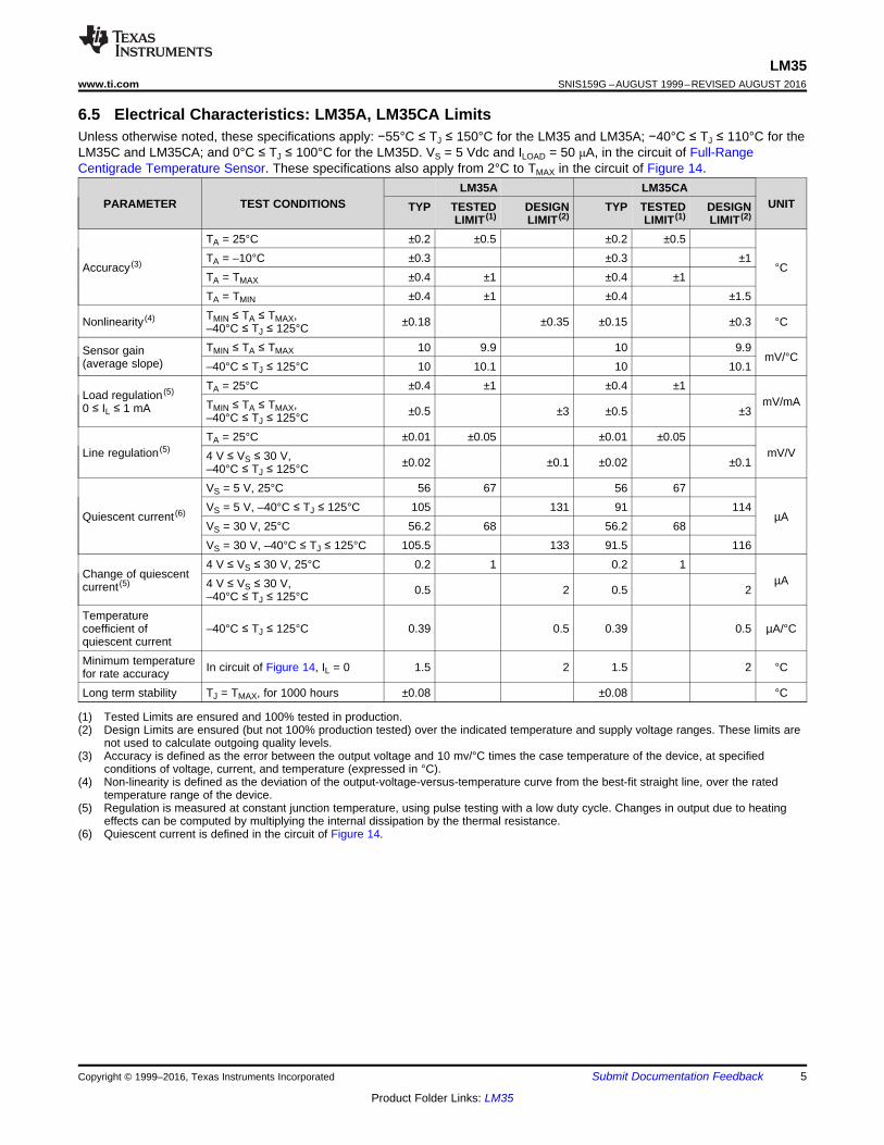
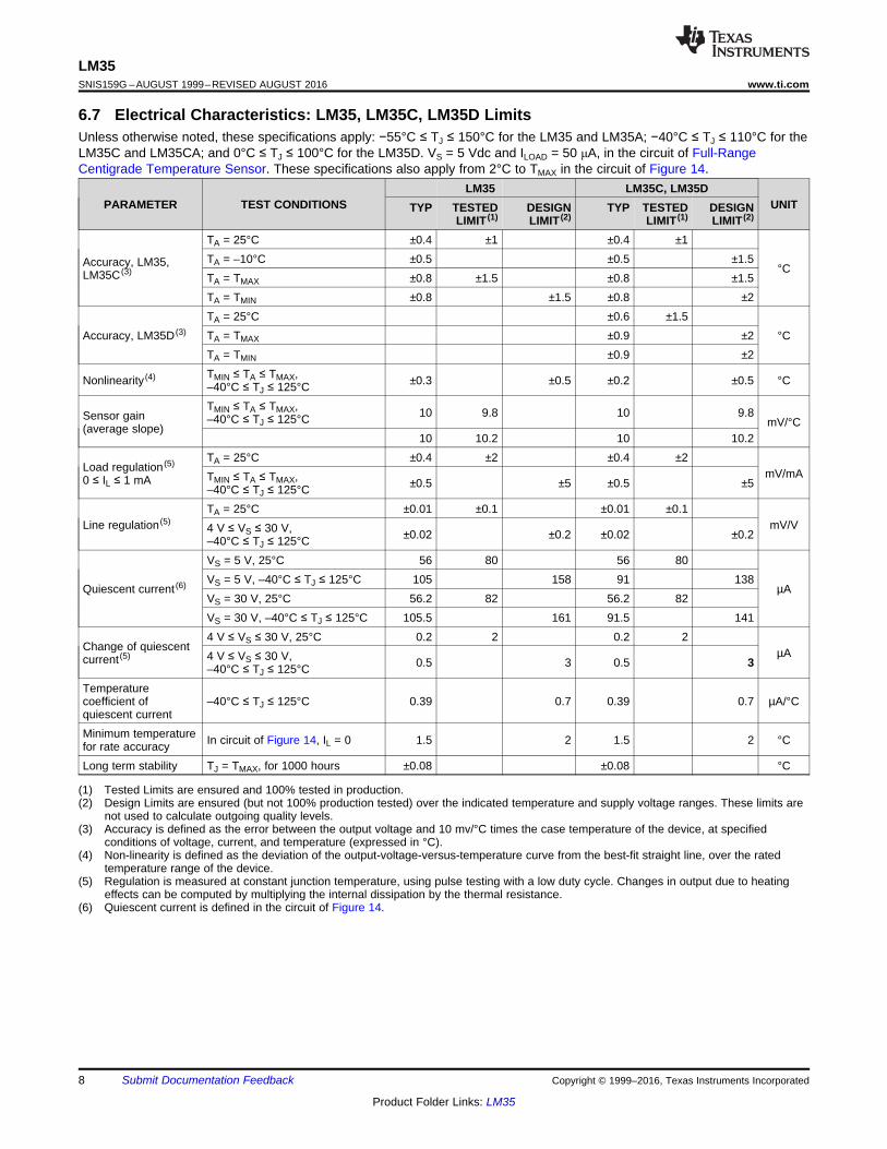
(1) Tested Limits are ensured and 100% tested in production.(2) Design Limits are ensured (but not 100% production tested) over the indicated temperature and supply voltage ranges. These limits are
not used to calculate outgoing quality levels.(3) Accuracy is defined as the error between the output voltage and 10 mv/°C times the case temperature of the device, at specified
conditions of voltage, current, and temperature (expressed in °C).(4) Non-linearity is defined as the deviation of the output-voltage-versus-temperature curve from the best-fit straight line, over the rated
temperature range of the device.(5) Regulation is measured at constant junction temperature, using pulse testing with a low duty cycle. Changes in output due to heating
effects can be computed by multiplying the internal dissipation by the thermal resistance.(6) Quiescent current is defined in the circuit of Figure 14.
6.5 Electrical Characteristics: LM35A, LM35CA LimitsUnless otherwise noted, these specifications apply: −55°C ≤ TJ ≤ 150°C for the LM35 and LM35A; −40°C ≤ TJ ≤ 110°C for theLM35C and LM35CA; and 0°C ≤ TJ ≤ 100°C for the LM35D. VS = 5 Vdc and ILOAD = 50 μA, in the circuit of Full-RangeCentigrade Temperature Sensor. These specifications also apply from 2°C to TMAX in the circuit of Figure 14.
PARAMETER TEST CONDITIONSLM35A LM35CA
UNITTYP TESTEDLIMIT (1)
DESIGNLIMIT (2)
TYP TESTEDLIMIT (1)
DESIGNLIMIT (2)
Accuracy (3)
TA = 25°C ±0.2 ±0.5 ±0.2 ±0.5
°CTA = –10°C ±0.3 ±0.3 ±1TA = TMAX ±0.4 ±1 ±0.4 ±1TA = TMIN ±0.4 ±1 ±0.4 ±1.5
Nonlinearity (4) TMIN ≤ TA ≤ TMAX,–40°C ≤ TJ ≤ 125°C ±0.18 ±0.35 ±0.15 ±0.3 °C
Sensor gain(average slope)
TMIN ≤ TA ≤ TMAX 10 9.9 10 9.9mV/°C
–40°C ≤ TJ ≤ 125°C 10 10.1 10 10.1
Load regulation (5)
0 ≤ IL ≤ 1 mA
TA = 25°C ±0.4 ±1 ±0.4 ±1mV/mATMIN ≤ TA ≤ TMAX,
–40°C ≤ TJ ≤ 125°C ±0.5 ±3 ±0.5 ±3
Line regulation (5)TA = 25°C ±0.01 ±0.05 ±0.01 ±0.05
mV/V4 V ≤ VS ≤ 30 V,–40°C ≤ TJ ≤ 125°C ±0.02 ±0.1 ±0.02 ±0.1
Quiescent current (6)
VS = 5 V, 25°C 56 67 56 67
µAVS = 5 V, –40°C ≤ TJ ≤ 125°C 105 131 91 114VS = 30 V, 25°C 56.2 68 56.2 68VS = 30 V, –40°C ≤ TJ ≤ 125°C 105.5 133 91.5 116
Change of quiescentcurrent (5)
4 V ≤ VS ≤ 30 V, 25°C 0.2 1 0.2 1µA4 V ≤ VS ≤ 30 V,
–40°C ≤ TJ ≤ 125°C 0.5 2 0.5 2
Temperaturecoefficient ofquiescent current
–40°C ≤ TJ ≤ 125°C 0.39 0.5 0.39 0.5 µA/°C
Minimum temperaturefor rate accuracy In circuit of Figure 14, IL = 0 1.5 2 1.5 2 °C
Long term stability TJ = TMAX, for 1000 hours ±0.08 ±0.08 °C
6
LM35SNIS159G –AUGUST 1999–REVISED AUGUST 2016 www.ti.com
Product Folder Links: LM35
Submit Documentation Feedback Copyright © 1999–2016, Texas Instruments Incorporated
(1) Accuracy is defined as the error between the output voltage and 10 mv/°C times the case temperature of the device, at specifiedconditions of voltage, current, and temperature (expressed in °C).
(2) Tested Limits are ensured and 100% tested in production.(3) Design Limits are ensured (but not 100% production tested) over the indicated temperature and supply voltage ranges. These limits are
not used to calculate outgoing quality levels.(4) Non-linearity is defined as the deviation of the output-voltage-versus-temperature curve from the best-fit straight line, over the rated
temperature range of the device.(5) Regulation is measured at constant junction temperature, using pulse testing with a low duty cycle. Changes in output due to heating
effects can be computed by multiplying the internal dissipation by the thermal resistance.
6.6 Electrical Characteristics: LM35A, LM35CAUnless otherwise noted, these specifications apply: −55°C ≤ TJ ≤ 150°C for the LM35 and LM35A; −40°C ≤ TJ ≤ 110°C for theLM35C and LM35CA; and 0°C ≤ TJ ≤ 100°C for the LM35D. VS = 5 Vdc and ILOAD = 50 μA, in the circuit of Full-RangeCentigrade Temperature Sensor. These specifications also apply from 2°C to TMAX in the circuit of Figure 14.
PARAMETER TEST CONDITIONSLM35A LM35CA
UNITMIN TYP MAX TYP TYP MAX
Accuracy (1)
TA = 25°C±0.2 ±0.2
°C
Tested Limit (2) ±0.5 ±0.5Design Limit (3)
TA = –10°C±0.3 ±0.3
Tested Limit (2)
Design Limit (3) ±1
TA = TMAX
±0.4 ±0.4Tested Limit (2) ±1 ±1Design Limit (3)
TA = TMIN
±0.4 ±0.4Tested Limit (2) ±1Design Limit (3) ±1.5
Nonlinearity (4) TMIN ≤ TA ≤ TMAX,–40°C ≤ TJ ≤ 125°C
±0.18 ±0.15°CTested Limit (2)
Design Limit (3) ±0.35 ±0.3
Sensor gain(average slope)
TMIN ≤ TA ≤ TMAX
10 10
mV/°C
Tested Limit (2) 9.9Design Limit (3) 9.9
–40°C ≤ TJ ≤ 125°C10 10
Tested Limit (2) 10.1Design Limit (3) 10.1
Load regulation (5)
0 ≤ IL ≤ 1 mA
TA = 25°C±0.4 ±0.4
mV/mA
Tested Limit (2) ±1 ±1Design Limit (3)
TMIN ≤ TA ≤ TMAX,–40°C ≤ TJ ≤ 125°C
±0.5 ±0.5Tested Limit (2)
Design Limit (3) ±3 ±3
Line regulation (5)
TA = 25°C±0.01 ±0.01
mV/V
Tested Limit (2) ±0.05 ±0.05Design Limit (3)
4 V ≤ VS ≤ 30 V,–40°C ≤ TJ ≤ 125°C
±0.02 ±0.02Tested Limit (2)
Design Limit (3) ±0.1 ±0.1
7
LM35www.ti.com SNIS159G –AUGUST 1999–REVISED AUGUST 2016
Product Folder Links: LM35
Submit Documentation FeedbackCopyright © 1999–2016, Texas Instruments Incorporated
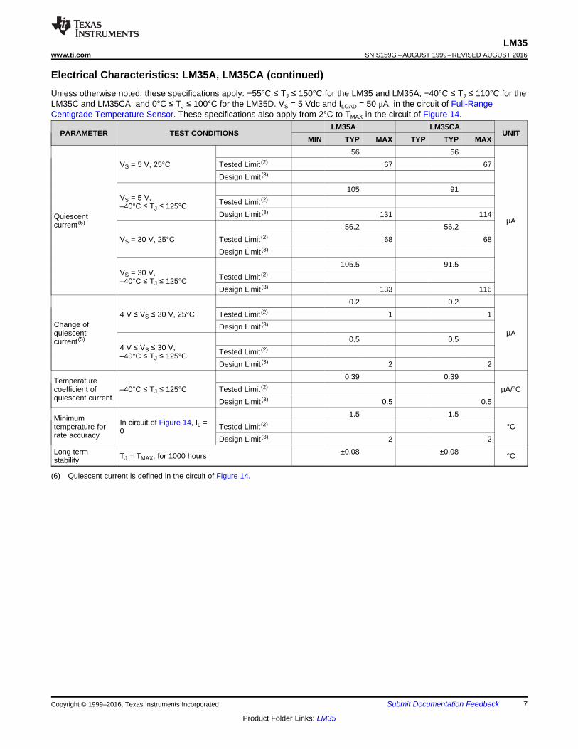
Electrical Characteristics: LM35A, LM35CA (continued)Unless otherwise noted, these specifications apply: −55°C ≤ TJ ≤ 150°C for the LM35 and LM35A; −40°C ≤ TJ ≤ 110°C for theLM35C and LM35CA; and 0°C ≤ TJ ≤ 100°C for the LM35D. VS = 5 Vdc and ILOAD = 50 μA, in the circuit of Full-RangeCentigrade Temperature Sensor. These specifications also apply from 2°C to TMAX in the circuit of Figure 14.
PARAMETER TEST CONDITIONSLM35A LM35CA
UNITMIN TYP MAX TYP TYP MAX
(6) Quiescent current is defined in the circuit of Figure 14.
Quiescentcurrent (6)
VS = 5 V, 25°C56 56
µA
Tested Limit (2) 67 67Design Limit (3)
VS = 5 V,–40°C ≤ TJ ≤ 125°C
105 91Tested Limit (2)
Design Limit (3) 131 114
VS = 30 V, 25°C56.2 56.2
Tested Limit (2) 68 68Design Limit (3)
VS = 30 V,–40°C ≤ TJ ≤ 125°C
105.5 91.5Tested Limit (2)
Design Limit (3) 133 116
Change ofquiescentcurrent (5)
4 V ≤ VS ≤ 30 V, 25°C0.2 0.2
µA
Tested Limit (2) 1 1Design Limit (3)
4 V ≤ VS ≤ 30 V,–40°C ≤ TJ ≤ 125°C
0.5 0.5Tested Limit (2)
Design Limit (3) 2 2
Temperaturecoefficient ofquiescent current
–40°C ≤ TJ ≤ 125°C0.39 0.39
µA/°CTested Limit (2)
Design Limit (3) 0.5 0.5
Minimumtemperature forrate accuracy
In circuit of Figure 14, IL =0
1.5 1.5°CTested Limit (2)
Design Limit (3) 2 2Long termstability TJ = TMAX, for 1000 hours ±0.08 ±0.08 °C
8
LM35SNIS159G –AUGUST 1999–REVISED AUGUST 2016 www.ti.com
Product Folder Links: LM35
Submit Documentation Feedback Copyright © 1999–2016, Texas Instruments Incorporated
(1) Tested Limits are ensured and 100% tested in production.(2) Design Limits are ensured (but not 100% production tested) over the indicated temperature and supply voltage ranges. These limits are
not used to calculate outgoing quality levels.(3) Accuracy is defined as the error between the output voltage and 10 mv/°C times the case temperature of the device, at specified
conditions of voltage, current, and temperature (expressed in °C).(4) Non-linearity is defined as the deviation of the output-voltage-versus-temperature curve from the best-fit straight line, over the rated
temperature range of the device.(5) Regulation is measured at constant junction temperature, using pulse testing with a low duty cycle. Changes in output due to heating
effects can be computed by multiplying the internal dissipation by the thermal resistance.(6) Quiescent current is defined in the circuit of Figure 14.
6.7 Electrical Characteristics: LM35, LM35C, LM35D LimitsUnless otherwise noted, these specifications apply: −55°C ≤ TJ ≤ 150°C for the LM35 and LM35A; −40°C ≤ TJ ≤ 110°C for theLM35C and LM35CA; and 0°C ≤ TJ ≤ 100°C for the LM35D. VS = 5 Vdc and ILOAD = 50 μA, in the circuit of Full-RangeCentigrade Temperature Sensor. These specifications also apply from 2°C to TMAX in the circuit of Figure 14.
PARAMETER TEST CONDITIONSLM35 LM35C, LM35D
UNITTYP TESTEDLIMIT (1)
DESIGNLIMIT (2)
TYP TESTEDLIMIT (1)
DESIGNLIMIT (2)
Accuracy, LM35,LM35C (3)
TA = 25°C ±0.4 ±1 ±0.4 ±1
°CTA = –10°C ±0.5 ±0.5 ±1.5TA = TMAX ±0.8 ±1.5 ±0.8 ±1.5TA = TMIN ±0.8 ±1.5 ±0.8 ±2
Accuracy, LM35D (3)
TA = 25°C ±0.6 ±1.5°CTA = TMAX ±0.9 ±2
TA = TMIN ±0.9 ±2
Nonlinearity (4) TMIN ≤ TA ≤ TMAX,–40°C ≤ TJ ≤ 125°C ±0.3 ±0.5 ±0.2 ±0.5 °C
Sensor gain(average slope)
TMIN ≤ TA ≤ TMAX,–40°C ≤ TJ ≤ 125°C 10 9.8 10 9.8
mV/°C10 10.2 10 10.2
Load regulation (5)
0 ≤ IL ≤ 1 mA
TA = 25°C ±0.4 ±2 ±0.4 ±2mV/mATMIN ≤ TA ≤ TMAX,
–40°C ≤ TJ ≤ 125°C ±0.5 ±5 ±0.5 ±5
Line regulation (5)TA = 25°C ±0.01 ±0.1 ±0.01 ±0.1
mV/V4 V ≤ VS ≤ 30 V,–40°C ≤ TJ ≤ 125°C ±0.02 ±0.2 ±0.02 ±0.2
Quiescent current (6)
VS = 5 V, 25°C 56 80 56 80
µAVS = 5 V, –40°C ≤ TJ ≤ 125°C 105 158 91 138VS = 30 V, 25°C 56.2 82 56.2 82VS = 30 V, –40°C ≤ TJ ≤ 125°C 105.5 161 91.5 141
Change of quiescentcurrent (5)
4 V ≤ VS ≤ 30 V, 25°C 0.2 2 0.2 2µA4 V ≤ VS ≤ 30 V,
–40°C ≤ TJ ≤ 125°C 0.5 3 0.5 3
Temperaturecoefficient ofquiescent current
–40°C ≤ TJ ≤ 125°C 0.39 0.7 0.39 0.7 µA/°C
Minimum temperaturefor rate accuracy In circuit of Figure 14, IL = 0 1.5 2 1.5 2 °C
Long term stability TJ = TMAX, for 1000 hours ±0.08 ±0.08 °C
9
LM35www.ti.com SNIS159G –AUGUST 1999–REVISED AUGUST 2016
Product Folder Links: LM35
Submit Documentation FeedbackCopyright © 1999–2016, Texas Instruments Incorporated
(1) Accuracy is defined as the error between the output voltage and 10 mv/°C times the case temperature of the device, at specifiedconditions of voltage, current, and temperature (expressed in °C).
(2) Tested Limits are ensured and 100% tested in production.(3) Design Limits are ensured (but not 100% production tested) over the indicated temperature and supply voltage ranges. These limits are
not used to calculate outgoing quality levels.(4) Non-linearity is defined as the deviation of the output-voltage-versus-temperature curve from the best-fit straight line, over the rated
temperature range of the device.(5) Regulation is measured at constant junction temperature, using pulse testing with a low duty cycle. Changes in output due to heating
effects can be computed by multiplying the internal dissipation by the thermal resistance.
6.8 Electrical Characteristics: LM35, LM35C, LM35DUnless otherwise noted, these specifications apply: −55°C ≤ TJ ≤ 150°C for the LM35 and LM35A; −40°C ≤ TJ ≤ 110°C for theLM35C and LM35CA; and 0°C ≤ TJ ≤ 100°C for the LM35D. VS = 5 Vdc and ILOAD = 50 μA, in the circuit of Full-RangeCentigrade Temperature Sensor. These specifications also apply from 2°C to TMAX in the circuit of Figure 14.
PARAMETER TEST CONDITIONSLM35 LM35C, LM35D
UNITMIN TYP MAX MIN TYP MAX
Accuracy, LM35,LM35C (1)
TA = 25°C±0.4 ±0.4
°C
Tested Limit (2) ±1 ±1Design Limit (3)
TA = –10°C±0.5 ±0.5
Tested Limit (2)
Design Limit (3) ±1.5
TA = TMAX
±0.8 ±0.8Tested Limit (2) ±1.5Design Limit (3) ±1.5
TA = TMIN
±0.8 ±0.8Tested Limit (2)
Design Limit (3) ±1.5 ±2
Accuracy,LM35D (1)
TA = 25°C±0.6
°C
Tested Limit (2) ±1.5Design Limit (3)
TA = TMAX
±0.9Tested Limit (2)
Design Limit (3) ±2
TA = TMIN
±0.9Tested Limit (2)
Design Limit (3) ±2
Nonlinearity (4) TMIN ≤ TA ≤ TMAX,–40°C ≤ TJ ≤ 125°C
±0.3 ±0.2°CTested Limit (2)
Design Limit (3) ±0.5 ±0.5
Sensor gain(average slope)
TMIN ≤ TA ≤ TMAX,–40°C ≤ TJ ≤ 125°C
10 10
mV/°C
Tested Limit (2) 9.8Design Limit (3) 9.8
10 10Tested Limit (2) 10.2Design Limit (3) 10.2
Load regulation (5)
0 ≤ IL ≤ 1 mA
TA = 25°C±0.4 ±0.4
mV/mA
Tested Limit (2) ±2 ±2Design Limit (3)
TMIN ≤ TA ≤ TMAX,–40°C ≤ TJ ≤ 125°C
±0.5 ±0.5Tested Limit (2)
Design Limit (3) ±5 ±5
10
LM35SNIS159G –AUGUST 1999–REVISED AUGUST 2016 www.ti.com
Product Folder Links: LM35
Submit Documentation Feedback Copyright © 1999–2016, Texas Instruments Incorporated
Electrical Characteristics: LM35, LM35C, LM35D (continued)Unless otherwise noted, these specifications apply: −55°C ≤ TJ ≤ 150°C for the LM35 and LM35A; −40°C ≤ TJ ≤ 110°C for theLM35C and LM35CA; and 0°C ≤ TJ ≤ 100°C for the LM35D. VS = 5 Vdc and ILOAD = 50 μA, in the circuit of Full-RangeCentigrade Temperature Sensor. These specifications also apply from 2°C to TMAX in the circuit of Figure 14.
PARAMETER TEST CONDITIONSLM35 LM35C, LM35D
UNITMIN TYP MAX MIN TYP MAX
(6) Quiescent current is defined in the circuit of Figure 14.
Line regulation (5)
TA = 25°C±0.01 ±0.01
mV/V
Tested Limit (2) ±0.1Design Limit (3) ±0.1
4 V ≤ VS ≤ 30 V,–40°C ≤ TJ ≤ 125°C
±0.02 ±0.02Tested Limit (2)
Design Limit (3) ±0.2 ±0.2
Quiescentcurrent (6)
VS = 5 V, 25°C56 56
µA
Tested Limit (2) 80 80Design Limit (3)
VS = 5 V, –40°C ≤ TJ ≤125°C
105 91Tested Limit (2)
Design Limit (3) 158 138
VS = 30 V, 25°C56.2 56.2
Tested Limit (2) 82 82Design Limit (3)
VS = 30 V,–40°C ≤ TJ ≤ 125°C
105.5 91.5Tested Limit (2)
Design Limit (3) 161 141
Change ofquiescentcurrent (5)
4 V ≤ VS ≤ 30 V, 25°C0.2 0.2
µA
Tested Limit (2) 2Design Limit (3) 2
4 V ≤ VS ≤ 30 V,–40°C ≤ TJ ≤ 125°C
0.5 0.5Tested Limit (2)
Design Limit (3) 3 3
Temperaturecoefficient ofquiescent current
–40°C ≤ TJ ≤ 125°C0.39 0.39
µA/°CTested Limit (2)
Design Limit (3) 0.7 0.7
Minimumtemperature forrate accuracy
In circuit of Figure 14, IL = 01.5 1.5
°CTested Limit (2)
Design Limit (3) 2 2Long termstability TJ = TMAX, for 1000 hours ±0.08 ±0.08 °C
0
20
40
60
80
100
120
140
160
±75 ±25 25 75 125 175
QU
IES
CE
NT
CU
RR
EN
T (�
A)
TEMPERATURE (�C) C006
2.4
2.6
2.8
3.0
3.2
3.4
3.6
3.8
4.0
4.2
4.4
±75 ±25 25 75 125 175
SU
PP
LY V
OLT
AG
E (
V)
TEMPERATURE (�C) C005
TYPICAL IOUT = 2.0 mA
TYPICAL IOUT = 1.0 mA
TYPICAL IOUT = 0 �A or 50 �A
±20
0
20
40
60
80
100
120
0 2 4 6 8
PE
RC
EN
T O
F F
INA
L V
ALU
E (
%)
TIME (MINUTES) C003
±20
0
20
40
60
80
100
120
0 2 4 6 8
PE
RC
EN
T O
F F
INA
L V
ALU
E (
%)
TIME (SEC) C004
T0-46
T0-92
0
100
200
300
400
0 400 800 1200 1600 2000
TH
ER
MA
L R
ES
IST
AN
CE
(�C
/W)
AIR VELOCITY (FPM) C001
T0-46
T0-92
0
5
10
15
20
25
30
35
40
45
0 400 800 1200 1600 2000
TIM
E C
ON
ST
AN
T (
SE
C)
AIR VELOCITY (FPM) C002
T0-46
T0-92
11
LM35www.ti.com SNIS159G –AUGUST 1999–REVISED AUGUST 2016
Product Folder Links: LM35
Submit Documentation FeedbackCopyright © 1999–2016, Texas Instruments Incorporated
6.9 Typical Characteristics
Figure 1. Thermal Resistance Junction To Air Figure 2. Thermal Time Constant
Figure 3. Thermal Response In Still Air Figure 4. Thermal Response In Stirred Oil Bath
Figure 5. Minimum Supply Voltage vs Temperature Figure 6. Quiescent Current vs Temperature (in Circuit ofFigure 14)

-20 -10 0 10 20 30 40 50 60 -0.2
0
0.2
0.4
0.6
0
2
4
6
TIME (�SEC) C011
VO
UT (
V)
VIN
(V
)
±2.5
±2.0
±1.5
±1.0
±0.5
0.0
0.5
1.0
1.5
2.0
2.5
±75 ±25 25 75 125 175
TE
MP
ER
AT
UR
E E
RR
OR
(�C
)
TEMPERATURE (�C) C009
LM35C
LM35CA
LM35D
LM35C
TYPICAL LM35CA
10 100 1k 10k 100k 0
200
400
600
800
1000
1200
1400
1600
Noi
se (
nV/�
Hz)
FREQUENCY (Hz) C010
40
60
80
100
120
140
160
180
200
±75 ±25 25 75 125 175
QU
IES
CE
NT
CU
RR
EN
T (�
A)
TEMPERATURE (�C) C007
±2.0
±1.5
±1.0
±0.5
0.0
0.5
1.0
1.5
2.0
±75 ±25 25 75 125 175
TE
MP
ER
AT
UR
E E
RR
OR
(�C
)
TEMPERATURE (�C) C008
LM35
LM35A
LM35
LM35A TYPICAL
12
LM35SNIS159G –AUGUST 1999–REVISED AUGUST 2016 www.ti.com
Product Folder Links: LM35
Submit Documentation Feedback Copyright © 1999–2016, Texas Instruments Incorporated
Typical Characteristics (continued)
Figure 7. Quiescent Current vs Temperature (in Circuit ofFull-Range Centigrade Temperature Sensor)
Figure 8. Accuracy vs Temperature (Ensured)
Figure 9. Accuracy vs Temperature (Ensured) Figure 10. Noise Voltage
Figure 11. Start-Up Response
.125 R2
VOUT = 10 mV/°C
+
+VS
R2
A2
A1
V0
nR1
i
8.8 mV/°C
nR1Q1 Q2
10E E
1.38 VPTAT
13
LM35www.ti.com SNIS159G –AUGUST 1999–REVISED AUGUST 2016
Product Folder Links: LM35
Submit Documentation FeedbackCopyright © 1999–2016, Texas Instruments Incorporated
7 Detailed Description
7.1 OverviewThe LM35-series devices are precision integrated-circuit temperature sensors, with an output voltage linearlyproportional to the Centigrade temperature. The LM35 device has an advantage over linear temperature sensorscalibrated in Kelvin, as the user is not required to subtract a large constant voltage from the output to obtainconvenient Centigrade scaling. The LM35 device does not require any external calibration or trimming to providetypical accuracies of ± ¼ °C at room temperature and ± ¾ °C over a full −55°C to 150°C temperature range.Lower cost is assured by trimming and calibration at the wafer level. The low output impedance, linear output,and precise inherent calibration of the LM35 device makes interfacing to readout or control circuitry especiallyeasy. The device is used with single power supplies, or with plus and minus supplies. As the LM35 device drawsonly 60 μA from the supply, it has very low self-heating of less than 0.1°C in still air. The LM35 device is rated tooperate over a −55°C to 150°C temperature range, while the LM35C device is rated for a −40°C to 110°C range(−10° with improved accuracy). The temperature-sensing element is comprised of a delta-V BE architecture.
The temperature-sensing element is then buffered by an amplifier and provided to the VOUT pin. The amplifierhas a simple class A output stage with typical 0.5-Ω output impedance as shown in the Functional BlockDiagram. Therefore the LM35 can only source current and it's sinking capability is limited to 1 μA.
7.2 Functional Block Diagram
7.3 Feature Description
7.3.1 LM35 Transfer FunctionThe accuracy specifications of the LM35 are given with respect to a simple linear transfer function:
VOUT = 10 mv/°C × T
where• VOUT is the LM35 output voltage• T is the temperature in °C (1)
7.4 Device Functional ModesThe only functional mode of the LM35 is that it has an analog output directly proportional to temperature.

LM35
+
OUT
HEAVY CAPACITIVE LOAD, WIRING, ETC.
TO A HIGH-IMPEDANCE LOAD
v75
1 PF
0.01 PF BYPASSOPTONAL
LM35
+
OUT
2 k
HEAVY CAPACITIVE LOAD, WIRING, ETC.
TO A HIGH-IMPEDANCE LOAD
v
14
LM35SNIS159G –AUGUST 1999–REVISED AUGUST 2016 www.ti.com
Product Folder Links: LM35
Submit Documentation Feedback Copyright © 1999–2016, Texas Instruments Incorporated
8 Application and Implementation
NOTEInformation in the following applications sections is not part of the TI componentspecification, and TI does not warrant its accuracy or completeness. TI’s customers areresponsible for determining suitability of components for their purposes. Customers shouldvalidate and test their design implementation to confirm system functionality.
8.1 Application InformationThe features of the LM35 make it suitable for many general temperature sensing applications. Multiple packageoptions expand on it's flexibility.
8.1.1 Capacitive Drive CapabilityLike most micropower circuits, the LM35 device has a limited ability to drive heavy capacitive loads. Alone, theLM35 device is able to drive 50 pF without special precautions. If heavier loads are anticipated, isolating ordecoupling the load with a resistor is easy (see Figure 12). The tolerance of capacitance can be improved with aseries R-C damper from output to ground (see Figure 13).
When the LM35 device is applied with a 200-Ω load resistor as shown in Figure 16, Figure 17, or Figure 19, thedevice is relatively immune to wiring capacitance because the capacitance forms a bypass from ground to inputand not on the output. However, as with any linear circuit connected to wires in a hostile environment,performance is affected adversely by intense electromagnetic sources (such as relays, radio transmitters, motorswith arcing brushes, and SCR transients), because the wiring acts as a receiving antenna and the internaljunctions act as rectifiers. For best results in such cases, a bypass capacitor from VIN to ground and a series R-Cdamper, such as 75 Ω in series with 0.2 or 1 μF from output to ground, are often useful. Examples are shown inFigure 13, Figure 24, and Figure 25.
Figure 12. LM35 with Decoupling from Capacitive Load
Figure 13. LM35 with R-C Damper
±2.0
±1.5
±1.0
±0.5
0.0
0.5
1.0
1.5
2.0
±75 ±25 25 75 125 175
TE
MP
ER
AT
UR
E E
RR
OR
(�C
)
TEMPERATURE (�C) C008
LM35
LM35A
LM35
LM35A TYPICAL
LM35
+VS
(4 V to 20 V)
OUTPUT
0 mV + 10.0 mV/°C
15
LM35www.ti.com SNIS159G –AUGUST 1999–REVISED AUGUST 2016
Product Folder Links: LM35
Submit Documentation FeedbackCopyright © 1999–2016, Texas Instruments Incorporated
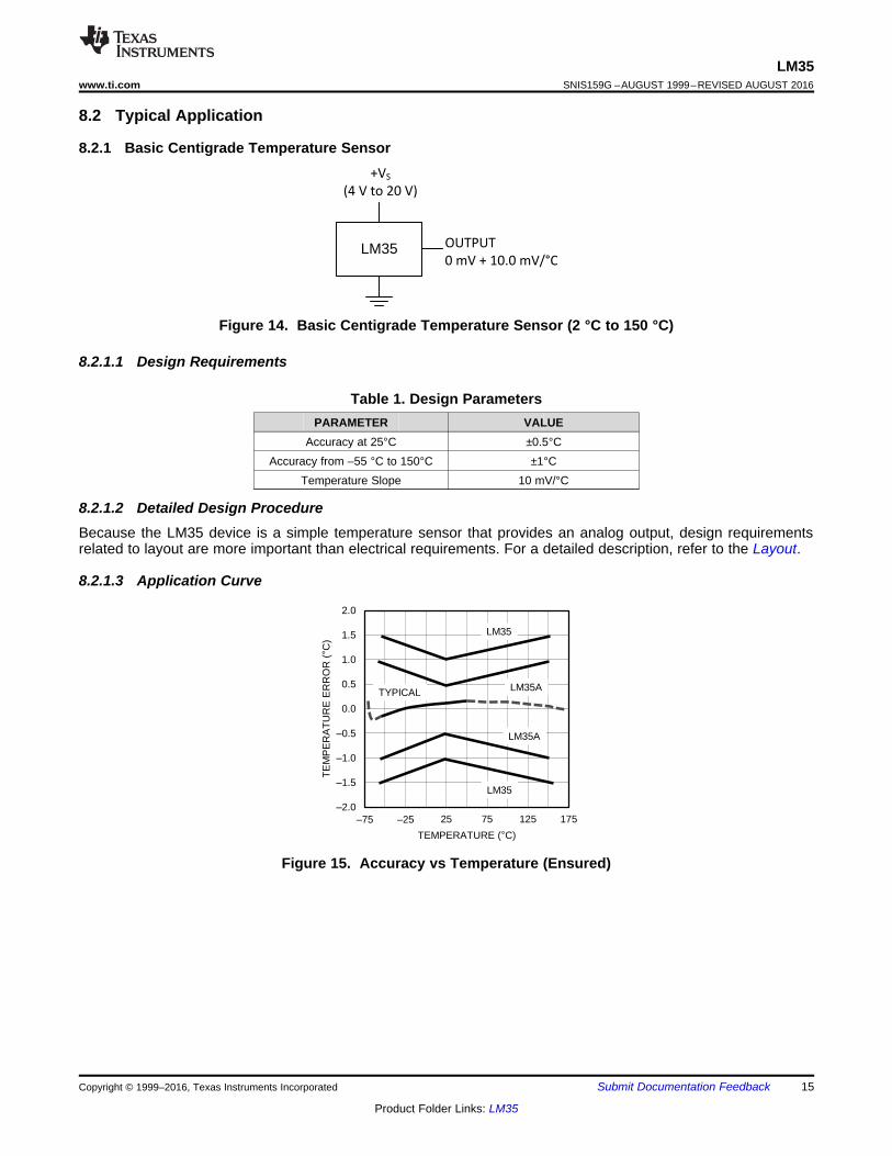
8.2 Typical Application
8.2.1 Basic Centigrade Temperature Sensor
Figure 14. Basic Centigrade Temperature Sensor (2 °C to 150 °C)
8.2.1.1 Design Requirements
Table 1. Design ParametersPARAMETER VALUE
Accuracy at 25°C ±0.5°CAccuracy from –55 °C to 150°C ±1°C
Temperature Slope 10 mV/°C
8.2.1.2 Detailed Design ProcedureBecause the LM35 device is a simple temperature sensor that provides an analog output, design requirementsrelated to layout are more important than electrical requirements. For a detailed description, refer to the Layout.
8.2.1.3 Application Curve
Figure 15. Accuracy vs Temperature (Ensured)
+VS
LM35
18 k
10%
VOUT
+
v
1N914
LM35
+
OUT
VOUT = 10 mV/°C (TAMBIENT = 10 °C)
FROM t 5 °C TO + 40 °C
5 V
200
1%
200
1%
TWISTED PAIR0.01 PF
BYPASSOPTIONAL
2 k
1%
2 k
1%
LM35
+
OUT
VOUT = 10 mV/°C (TAMBIENT = 1 °C)
FROM + 2 °C TO + 40 °C
v
5 V
200
1%
6.8 k
5%
200
1%
TWISTED PAIR
HEAT
FINS
+
v
LM35
+
OUT
VOUT = 10 mV/°C (TAMBIENT = 1 °C)
FROM + 2 °C TO + 40 °C
v
5 V
200
1%
6.8 k
5%
OR 10K RHEOSTAT
FOR GAIN ADJUST
200
1%
TWISTED PAIR
HEAT
FINS
16
LM35SNIS159G –AUGUST 1999–REVISED AUGUST 2016 www.ti.com
Product Folder Links: LM35
Submit Documentation Feedback Copyright © 1999–2016, Texas Instruments Incorporated
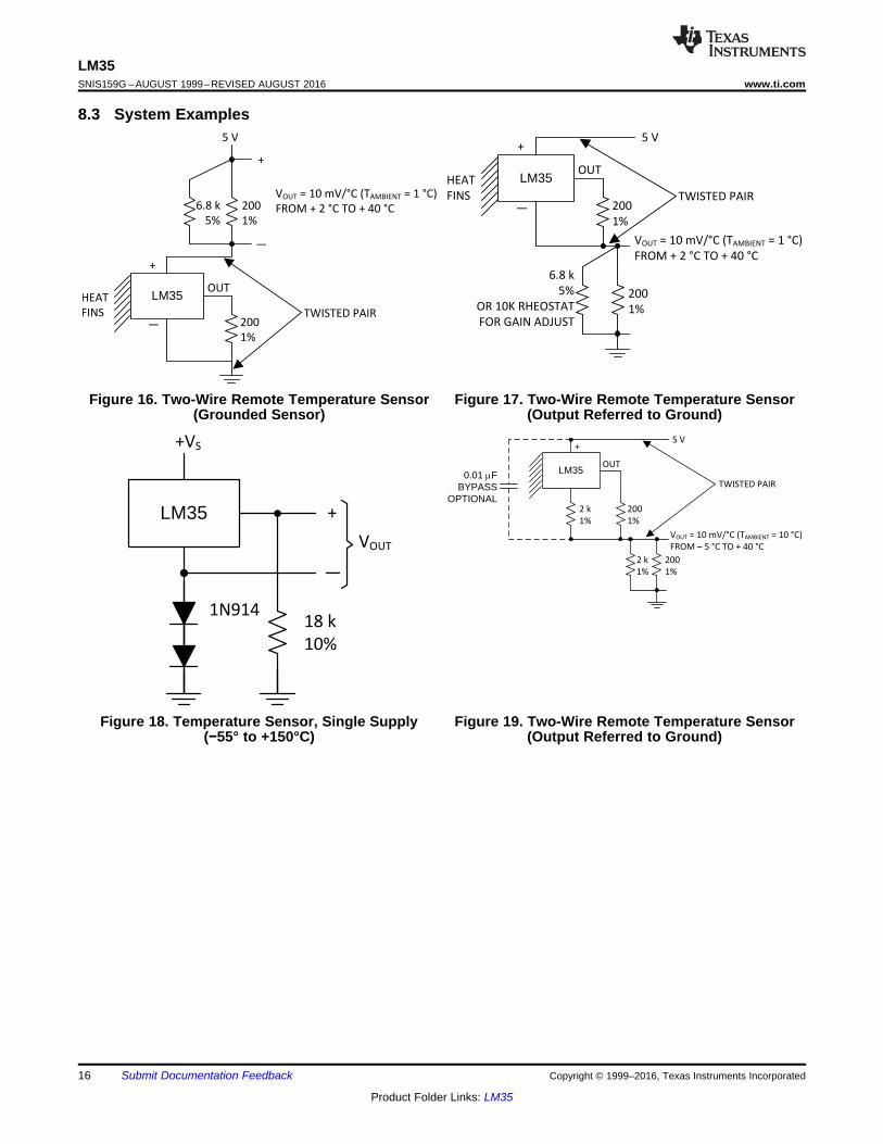
8.3 System Examples
Figure 16. Two-Wire Remote Temperature Sensor(Grounded Sensor)
Figure 17. Two-Wire Remote Temperature Sensor(Output Referred to Ground)
Figure 18. Temperature Sensor, Single Supply(−55° to +150°C)
Figure 19. Two-Wire Remote Temperature Sensor(Output Referred to Ground)
LM35
9 V
1 k
25.5 kLM385-2.5
100 �A,60 mVFULL-SCALE
LM35
5 V
LM35
+VS
(6 V to 20 V)
45.5 kO
1%
10 kO
1%
26.4 kO
1%
1 MO
1%
18 kOLM385-1.2
VOUT = +1 mV/°F
LM35 LM317
402
1%
50
OUT
OFFSET
ADJUST
+
v
OUT
62.5
0.5%
4.7 k
IN
ADJ
+ 5 V TO + 30 V
2N2907
17
LM35www.ti.com SNIS159G –AUGUST 1999–REVISED AUGUST 2016
Product Folder Links: LM35
Submit Documentation FeedbackCopyright © 1999–2016, Texas Instruments Incorporated
System Examples (continued)
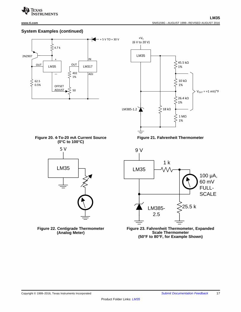
Figure 20. 4-To-20 mA Current Source(0°C to 100°C)
Figure 21. Fahrenheit Thermometer
Figure 22. Centigrade Thermometer(Analog Meter)
Figure 23. Fahrenheit Thermometer, ExpandedScale Thermometer
(50°F to 80°F, for Example Shown)

LM35
+
OUT
200*
1.5 k*
HEAT
FINS
VA
RA
1 k
1 PF+
20 PF+
LM3914 LM3914
1.2 k*
67 68 69 70 71 72 73 74 75 76 77 78 79 80 81 82 83 84 85 86
10
20 k
18
1 2 3
7 V
4 5 6 7 8 9 1 2 3 4 5 6 7 8 9
NC
VBVC
499*499*
10 18
7 V
7 V
1.5 k*
RC
1 k
1 k*
RB
1 k
20 LEDs
°F
LM35LM131
47
+
GND
8
6 V
100 k
0.01 PF100 k 1 PF
12 k
5 k
FULLSCALEADJ
1 2 4
6
7
0.01 PF
LOW TEMPCO
3
5
1 k6.8 k
4N28
fOUT
LM35
+
OUT
GND
75
1 PF
16 k
ADC0804
+2 k
1 k +
IN
VREF
0.64 V
5 V
8PARALLEL
DATA
OUTPUT
INTR
CS
RD
WR
GND
LM35
+
OUT
GND
75
1 PF
3.9 k
+
10 k
100k+
IN
5 V
SERIAL
DATA OUTPUT
CLOCK
ENABLE
GND
ADC08031
LM385FB
REF
1.28 V
18
LM35SNIS159G –AUGUST 1999–REVISED AUGUST 2016 www.ti.com
Product Folder Links: LM35
Submit Documentation Feedback Copyright © 1999–2016, Texas Instruments Incorporated
System Examples (continued)
Figure 24. Temperature to Digital Converter(Serial Output)
(128°C Full Scale)
Figure 25. Temperature to Digital Converter(Parallel TRI-STATE Outputs for Standard Data Bus
to μP Interface)(128°C Full Scale)
*=1% or 2% film resistorTrim RB for VB = 3.075 VTrim RC for VC = 1.955 VTrim RA for VA = 0.075 V + 100 mV/°C ×Tambient
Example, VA = 2.275 V at 22°C
Figure 26. Bar-Graph Temperature Display(Dot Mode)
Figure 27. LM35 With Voltage-To-FrequencyConverter and Isolated Output(2°C to 150°C; 20 to 1500 Hz)

19
LM35www.ti.com SNIS159G –AUGUST 1999–REVISED AUGUST 2016
Product Folder Links: LM35
Submit Documentation FeedbackCopyright © 1999–2016, Texas Instruments Incorporated
9 Power Supply RecommendationsThe LM35 device has a very wide 4-V to 30-V power supply voltage range, which makes it ideal for manyapplications. In noisy environments, TI recommends adding a 0.1 μF from V+ to GND to bypass the powersupply voltage. Larger capacitances maybe required and are dependent on the power-supply noise.
(1) Wakefield type 201, or 1-in disc of 0.02-in sheet brass, soldered to case, or similar.(2) TO-92 and SOIC-8 packages glued and leads soldered to 1-in square of 1/16-in printed circuit board with 2-oz foil or similar.
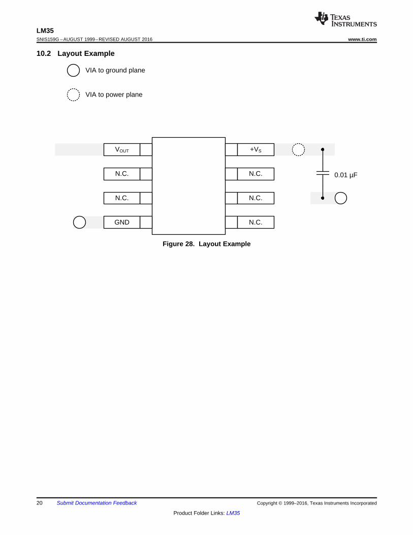
10 Layout
10.1 Layout GuidelinesThe LM35 is easily applied in the same way as other integrated-circuit temperature sensors. Glue or cement thedevice to a surface and the temperature should be within about 0.01°C of the surface temperature.
The 0.01°C proximity presumes that the ambient air temperature is almost the same as the surface temperature.If the air temperature were much higher or lower than the surface temperature, the actual temperature of theLM35 die would be at an intermediate temperature between the surface temperature and the air temperature;this is especially true for the TO-92 plastic package. The copper leads in the TO-92 package are the principalthermal path to carry heat into the device, so its temperature might be closer to the air temperature than to thesurface temperature.
Ensure that the wiring leaving the LM35 device is held at the same temperature as the surface of interest tominimize the temperature problem. The easiest fix is to cover up these wires with a bead of epoxy. The epoxybead will ensure that the leads and wires are all at the same temperature as the surface, and that thetemperature of the LM35 die is not affected by the air temperature.
The TO-46 metal package can also be soldered to a metal surface or pipe without damage. Of course, in thatcase the V− terminal of the circuit will be grounded to that metal. Alternatively, mount the LM35 inside a sealed-end metal tube, and then dip into a bath or screw into a threaded hole in a tank. As with any IC, the LM35 deviceand accompanying wiring and circuits must be kept insulated and dry, to avoid leakage and corrosion. This isespecially true if the circuit may operate at cold temperatures where condensation can occur. Printed-circuitcoatings and varnishes such as a conformal coating and epoxy paints or dips are often used to insure thatmoisture cannot corrode the LM35 device or its connections.
These devices are sometimes soldered to a small light-weight heat fin to decrease the thermal time constant andspeed up the response in slowly-moving air. On the other hand, a small thermal mass may be added to thesensor, to give the steadiest reading despite small deviations in the air temperature.
Table 2. Temperature Rise of LM35 Due To Self-heating (Thermal Resistance, RθJA)
TO, no heatsink
TO (1), smallheat fin
TO-92, no heatsink
TO-92 (2), smallheat fin
SOIC-8, noheat sink
SOIC-8 (2),small heat
finTO-220, noheat sink
Still air 400°C/W 100°C/W 180°C/W 140°C/W 220°C/W 110°C/W 90°C/WMoving air 100°C/W 40°C/W 90°C/W 70°C/W 105°C/W 90°C/W 26°C/WStill oil 100°C/W 40°C/W 90°C/W 70°C/W — — —Stirred oil 50°C/W 30°C/W 45°C/W 40°C/W — — —(Clamped tometal, Infiniteheat sink)
(24°C/W) — — (55°C/W) —
VOUT
N.C.
N.C.
+VS
N.C.
0.01 µF
VIA to ground plane
VIA to power plane
GND N.C.
N.C.
20
LM35SNIS159G –AUGUST 1999–REVISED AUGUST 2016 www.ti.com
Product Folder Links: LM35
Submit Documentation Feedback Copyright © 1999–2016, Texas Instruments Incorporated
10.2 Layout Example
Figure 28. Layout Example