lm5045 full-bridge pwm controller with integrated mosfet ... · lm5045 full-bridge pwm controller...
TRANSCRIPT

Vout
T1T1
Vin
ISOLATED FEEDBACK SSOFF
VCC
REF AGNDPGNDSSRESRT
UVLO
VIN
HO1 BST1 HS1 LO1 CS LO2 HS2 BST2 HO2
COMP
LM5045 FULL-BRIDGE CONTROLLERWITH INTEGRATED GATE DRIVERS
RD1 RD2
GATEDRIVE
ISOLATION
SR1
SR2
VCC VCC
ISOLATION BOUNDARY
SLOPE RAMP
SSSR
OVP
Product
Folder
Sample &Buy
Technical
Documents
Tools &
Software
Support &Community
LM5045SNVS699H –FEBRUARY 2011–REVISED JANUARY 2015
LM5045 Full-Bridge PWM Controller With Integrated MOSFET Drivers1 Features 3 Description
The LM5045 PWM controller contains all of the1• Highest Integration Controller for Small Form
features necessary to implement full-bridge topologyFactor, High-Density Power Converterspower converters using either current mode or
• High-Voltage Start-Up Regulator voltage mode control. This device is intended to• Intelligent Sync Rectifier Start-Up Allows Linear operate on the primary side of an isolated DC-DC
converter with input voltage up to 100 V. This highlyTurnon Into Prebiased Loadsintegrated controller-driver provides dual 2-A high-• Synchronous Rectifiers Disabled in UVLO modeside and low-side gate drivers for the four externaland Hiccup Mode bridge MOSFETs plus control signals for the
• Two Independent, Programmable Synchronous secondary-side synchronous rectifier MOSFETs.Rectifier Dead-Time Adjustments External resistors program the leading and trailing
edge dead-time between the main and synchronous• Four High-Current 2-A Bridge Gate Driversrectifier control signals. Intelligent start-up of the• Wide-Bandwidth Optocoupler Interfacesynchronous rectifiers allows monotonic turnon of the
• Configurable for Either Current Mode or Voltage power converter even with prebias load conditions.Mode Control Additional features include cycle-by-cycle current
limiting, hiccup mode restart, programmable soft-• Dual-Mode Overcurrent Protectionstart, synchronous rectifier soft-start, and a 2-MHz• Resistor Programmed 2-MHz Oscillatorcapable oscillator with synchronization capability and
• Programmable Line UVLO and OVP thermal shutdown.
2 Applications Device Information(1)
PART NUMBER PACKAGE BODY SIZE (NOM)• E-BikeHTSSOP (28) 9.70 mm × 4.40 mm• Military: Radar and Electronic Warfare LM5045WQFN (28) 5.00 mm × 5.00 mm• Power: Telecom DC-DC Module: Analog
(1) For all available packages, see the orderable addendum at• Private Branch Exchange (PBX)the end of the data sheet.
• Solar Power Inverters• Vector Signal Generators• Microwave Ovens• Point-to-Point Microwave Backhaul• Power: Telecom/Server AC/DC Supply: Dual
Controller: Analog• Solar Micro-Inverters• TETRA Base Stations• Washing Machine: Low-End
Simplified Full-Bridge Power Converter
1
An IMPORTANT NOTICE at the end of this data sheet addresses availability, warranty, changes, use in safety-critical applications,intellectual property matters and other important disclaimers. PRODUCTION DATA.
LM5045SNVS699H –FEBRUARY 2011–REVISED JANUARY 2015 www.ti.com
Table of Contents7.3 Feature Description................................................. 141 Features .................................................................. 17.4 Device Functional Modes........................................ 222 Applications ........................................................... 1
8 Application and Implementation ........................ 253 Description ............................................................. 18.1 Application Information............................................ 254 Revision History..................................................... 28.2 Typical Application .................................................. 255 Pin Configuration and Functions ......................... 3
9 Power Supply Recommendations ...................... 346 Specifications......................................................... 610 Layout................................................................... 346.1 Absolute Maximum Ratings ..................................... 6
10.1 Layout Guidelines ................................................. 346.2 ESD Ratings ............................................................ 610.2 Layout Example .................................................... 356.3 Recommended Operating Conditions....................... 6
11 Device and Documentation Support ................. 376.4 Thermal Information .................................................. 611.1 Trademarks ........................................................... 376.5 Electrical Characteristics........................................... 711.2 Electrostatic Discharge Caution............................ 376.6 Typical Characteristics ............................................ 1011.3 Glossary ................................................................ 377 Detailed Description ............................................ 12
12 Mechanical, Packaging, and Orderable7.1 Overview ................................................................. 12Information ........................................................... 377.2 Functional Block Diagram ....................................... 13
4 Revision HistoryNOTE: Page numbers for previous revisions may differ from page numbers in the current version.
Changes from Revision G (March 2013) to Revision H Page
• Added Pin Configuration and Functions section, ESD Ratings table, Feature Description section, Device FunctionalModes, Application and Implementation section, Power Supply Recommendations section, Layout section, Deviceand Documentation Support section, and Mechanical, Packaging, and Orderable Information section .............................. 1
Changes from Revision F (March 2013) to Revision G Page
• Changed layout of National Data Sheet to TI format ........................................................................................................... 25
2 Submit Documentation Feedback Copyright © 2011–2015, Texas Instruments Incorporated
Product Folder Links: LM5045
SS
RE
S
HS
2
HO
2
BS
T2
SS
SR
REF
RT
SLOPE
RD2
COMP
AGND
RD1
PGND
LO1
VCC
LO2
BST1
SS
OF
F
SR1
OV
P
RA
MP
UV
LO
CS
HS
1
HO
1
VIN
SR2
1
2
3
4
5
6
7
21
20
19
18
17
16
15
8 9 10 11 12 13 14
28 27 26 25 24 23 22
VIN
PGND
LO1
VCC
LO2
SR2
SR1
HS2
HO2
BST2
HS1
BST1
HO1
COMP
RD2
UVLO
OVP
CS
RAMP
SSSR
AGND
SLOPE
RT
REF
RD1
SS
SS OFF
RES
4
6
5
3
2
1
7
8
9
10
11
12
13
14
20
19
18
17
16
15
26
25
24
23
22
21
28
27
PowerPAD™
LM5045www.ti.com SNVS699H –FEBRUARY 2011–REVISED JANUARY 2015
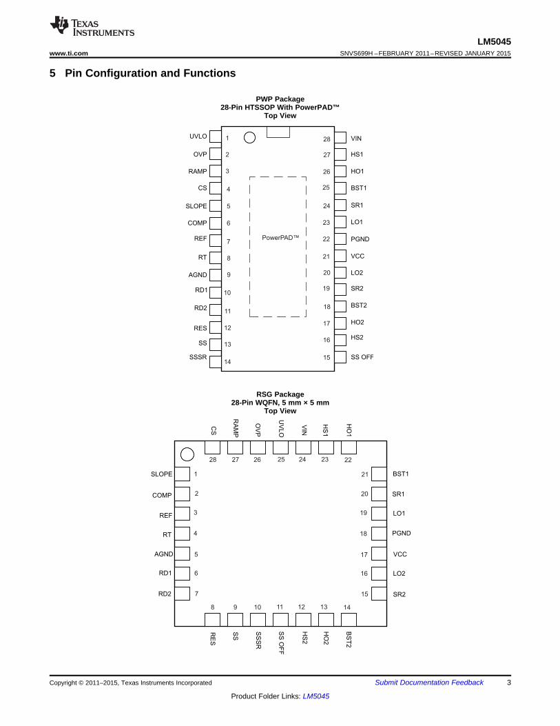
5 Pin Configuration and Functions
PWP Package28-Pin HTSSOP With PowerPAD™
Top View
RSG Package28-Pin WQFN, 5 mm × 5 mm
Top View
Copyright © 2011–2015, Texas Instruments Incorporated Submit Documentation Feedback 3
Product Folder Links: LM5045

LM5045SNVS699H –FEBRUARY 2011–REVISED JANUARY 2015 www.ti.com
Pin FunctionsPIN
I/O DESCRIPTION APPLICATION INFORMATIONNAME HTSSOP WQFNAGND 9 5 O Analog Ground Connect directly to the Power Ground.BST1 25 21 Bootstrap capacitors connected between BST1, 2 and SW1,
2 provide bias supply for the high side HO1, 2 gate drivers.I Gate Drive Bootstrap External diodes are required between VCC and BST1, 2 toBST2 18 14charge the bootstrap capacitors when SW1, 2 are low.An external opto-coupler connected to the COMP pinsources current into an internal NPN current mirror. The
Input to the Pulse Width PWM duty cycle is at maximum with zero input current, whileCOMP 6 2 I Modulator 1 mA reduces the duty cycle to zero. The current mirrorimproves the frequency response by reducing the AC voltageacross the opto-coupler.If CS exceeds 750 mV the PWM output pulse will beterminated, entering cycle-by-cycle current limit. An internalCS 4 28 I Current Sense Input switch holds CS low for 40 nS after either output switcheshigh to blank leading edge transients.
HO1 26 22 High side PWM outputs capable of driving the upperO High Side Output Driver MOSFET of the bridge with 1.5-A peak source and 2-A peak
HO2 17 13 sink current.HS1 27 23 Common connection of the high side FET source, low sideI Switch Node FET drain and transformer primary winding.HS2 16 12LO1 23 19 Alternating output of the PWM gate driver. Capable of 1.5-AO Low Side Output Driver peak source and 2-A peak sink current.LO2 20 16
An external voltage divider from the input power supply setsthe shutdown level during an over-voltage condition.Alternatively, an external NTC thermistor voltage divider canOVP/OTP 2 26 I Overvoltage Protection be used to set the shutdown temperature. The threshold is1.25 V. Hysteresis is set by an internal current that sources20 µA of current into the external resistor divider.
PGND 22 18 O Power Ground Connect directly to Analog GroundModulation ramp for the PWM comparator. This ramp can bea signal representative of the primary current (current mode)RAMP 3 27 I Input to PWM Comparator or proportional to the input voltage (feed-forward voltagemode). This pin is reset to GND at the end of every cycle.The resistance connected between RD1 and AGND sets theSynchronous RectifierRD1 10 6 I delay from the falling edge of SR1 or SR2 and the risingLeading Edge Delay edge of HO2/LO1 or HO1/LO2, respectively.The resistance connected between RD2 and AGND sets theSynchronous RectifierRD2 11 7 I delay from the falling edge of HO1/LO2 or HO2/LO1 and theTrailing Edge Delay rising edge of SR2 or SR1, respectively.Maximum output current is 15 mA. Locally decouple with aREF 7 3 O Output of a 5V reference 0.1-µF capacitor.Whenever the CS pin exceeds the 750-mV cycle-cyclecurrent limit threshold, 30-µA current is sourced into the REScapacitor for the remainder of the PWM cycle. If the REScapacitor voltage reaches 1.0 V, the SS capacitor isdischarged to disable the HO1, HO2, LO1, LO2 and SR1,RES 12 8 I Restart Timer SR2 outputs. The SS pin is held low until the voltage on theRES capacitor has been ramped between 2-V and 4-V eighttimes by 10-µA charge and 5-µA discharge currents. Afterthe delay sequence, the SS capacitor is released to initiate anormal start-up sequence.The resistance connected between RT and AGND sets theOscillator Frequency oscillator frequency. Synchronization is achieved by ACRT/SYNC 8 4 O Control and Frequency coupling a pulse to the RT/SYNC pin that raises the voltageSynchronization at least 1.5 V above the 2-V nominal bias level.A ramping current source from 0 to 100 µA is provided forslope compensation in current mode control. This pin can beSlope CompensationSLOPE 5 1 O connected through an appropriate resistor to the CS pin toCurrent provide slope compensation. If slope compensation is notrequired, SLOPE must be tied to ground.
4 Submit Documentation Feedback Copyright © 2011–2015, Texas Instruments Incorporated
Product Folder Links: LM5045

LM5045www.ti.com SNVS699H –FEBRUARY 2011–REVISED JANUARY 2015
Pin Functions (continued)PIN
I/O DESCRIPTION APPLICATION INFORMATIONNAME HTSSOP WQFN
Synchronous Rectifier Control output for synchronous rectifier gate. Capable ofSR1 24 20 O Driver peak sourcing 100 mA and sinking 400 mA.Synchronous Rectifier Control output for synchronous rectifier gate. Capable ofSR2 19 15 O Driver peak sourcing 100 mA and sinking 400 mA.
An internal 20-µA current source charges the SS pin duringstart-up. The input to the PWM comparator gradually rises asthe SS capacitor charges to steadily increase the PWM dutySS 13 9 I Soft-Start Input cycle. Pulling the SS pin to a voltage below 20 0mV stopsPWM pulses at HO1, 2 and LO1, 2 and turns off thesynchronous rectifier FETs to a low state.When SS OFF pin is connected to the AGND, the LM5045soft-stops in the event of a VIN UVLO and Hiccup mode
SSOFF 15 11 I Soft-Stop Disable current limit condition. If the SSOFF pin is connected to REFpin, the controller hard-stops on any fault condition. Refer toTable 1 for more details.An external capacitor and an internal 20-µA current sourceset the soft-start ramp for the synchronous rectifiers. TheSSSR 14 10 I Secondary Side Soft-Start SSSR capacitor charge-up is enabled after the first outputpulse and SS > 2 V and Icomp < 800 µAAn external voltage divider from the power source sets theshutdown and standby comparator levels. When UVLOreaches the 0.4-V threshold the VCC and REF regulators areLine UndervoltageUVLO 1 25 I enabled. At the 1.25-V threshold, the SS pin is released andLockout the controller enters the active mode. Hysteresis is set by aninternal current sink that pulls 20 µA from the externalresistor divider.The output voltage of the start-up regulator is initiallyregulated to 9.5 V. Once the secondary side soft-start (SSSR
Output of Start-Up pin) reaches 1 V, the VCC output is reduced to 7.7 V. If anVCC 21 17 I Regulator auxiliary winding raises the voltage on this pin above theregulation set-point, the internal start-up regulator willshutdown, thus reducing the IC power dissipation.Input to the Start-up Regulator. Operating input range is 14 Vto 100 V. For power sources outside of this range, theVIN 28 24 I Input Power Source LM5045 can be biased directly at VCC by an externalregulator.
Copyright © 2011–2015, Texas Instruments Incorporated Submit Documentation Feedback 5
Product Folder Links: LM5045

LM5045SNVS699H –FEBRUARY 2011–REVISED JANUARY 2015 www.ti.com
6 Specifications
6.1 Absolute Maximum Ratings (1)
MIN MAX UNITVIN to GND –0.3 105 VHS to GND (2) –5 105 VBST1/BST2 to GND –0.3 116 VBST1/BST2 to HS1/HS2 –0.3 16 VHO1/HO2 to HS1/HS2 (3) –0.3 BST1/BST2 + 0.3 VLO1/LO2/SR1/SR2 (3) –0.3 VCC + 0.3 VVCC to GND –0.3 16 VREF,SSOFF,RT,OVP,UVLO to GND –0.3 7 VRAMP –0.3 7 VCOMP –0.3 VCOMP Input Current 10 mAAll other inputs to GND (3) –0.3 REF + 0.3 VJunction Temperature 150 °CStorage temperature, Tstg –55 150 °C
(1) Absolute Maximum Ratings are limits beyond which damage to the device may occur. Operating Ratings are conditions under whichoperation of the device is intended to be functional. For ensured specifications and test conditions, see the Electrical Characteristics.
(2) The negative HS voltage must never be more negative than VCC–16 V. For example, if VCC = 12 V, the negative transients at HS mustnot exceed –4 V.
(3) These pins are output pins and as such should not be connected to an external voltage source. The voltage range listed is the limits theinternal circuitry is designed to reliably tolerate in the application circuit.
6.2 ESD RatingsVALUE UNIT
Human body model (HBM), per ANSI/ESDA/JEDEC JS-001 (1) ±2000V(ESD) Electrostatic discharge VCharged-device model (CDM), per JEDEC specification JESD22- ±750
C101 (2)
(1) JEDEC document JEP155 states that 500-V HBM allows safe manufacturing with a standard ESD control process.(2) JEDEC document JEP157 states that 250-V CDM allows safe manufacturing with a standard ESD control process.
6.3 Recommended Operating Conditionsover operating free-air temperature range (unless otherwise noted)
MIN NOM MAX UNITVIN Voltage 14 100 VExternal Voltage Applied to VCC 10 14 VJunction Temperature –40 125 °CSLOPE –0.3 2 V
6.4 Thermal InformationLM5045
THERMAL METRIC (1) PWP RSG UNIT28 PINS
RθJA Junction-to-ambient thermal resistance 40 40°C/W
RθJC(top) Junction-to-case (top) thermal resistance 4 4
(1) For more information about traditional and new thermal metrics, see the IC Package Thermal Metrics application report, SPRA953.
6 Submit Documentation Feedback Copyright © 2011–2015, Texas Instruments Incorporated
Product Folder Links: LM5045

LM5045www.ti.com SNVS699H –FEBRUARY 2011–REVISED JANUARY 2015
6.5 Electrical CharacteristicsLimits in standard typeface are for TJ = 25°C only; MIN and MAX limits apply the junction temperature range of –40°C to125°C. Unless otherwise specified, the following conditions apply: VIN = 48 V, RT = 25 kΩ, RD1 = RD2 = 20 kΩ. No load onHO1, HO2, LO1, LO2, SR1, SR2, COMP = 0 V, UVLO = 2.5 V, OVP = 0 V, SSOFF = 0 V.
PARAMETER TEST CONDITIONS MIN TYP MAX UNITSTART-UP REGULATOR (VCC PIN)VCC1 VCC voltage ICC= 10 mA (SSSR < 1 V) 9.3 9.6 9.9 VVCC2 VCC voltage ICC= 10 mA (SSSR > 1 V) 7.5 7.8 8.1 VICC(Lim) VCC current limit VCC= 6 V 60 80 mAICC(ext) VCC supply current Supply current into VCC from an 4.6 mA
externally applied source. VCC = 10V
VCC load regulation ICC from 0 to 50 mA 35 mVVCC(UV) VCC undervoltage threshold Positive going VCC VCC1–0.2 VCC1–0.1 V
Negative going VCC 5.9 6.3 6.7 VIIN VIN operating current 4 mA
VIN shutdown current VIN = 20 V, VUVLO = 0 V 300 520 µAVIN = 100 V, VUVLO = 0 V 350 550 µA
VIN start-up regulator leakage VCC=10 V 160 µAVOLTAGE REFERENCE REGULATOR (REF PIN)VREF REF voltage IREF = 0 mA 4.85 5 5.15 V
REF voltage regulation IREF = 0 to 10 mA 25 50 mVIREF(Lim) REF current limit VREF = 4.5 V 15 20 mAVREFUV VREF undervoltage threshold Positive going VREF 4.3 4.5 4.7 V
Hysteresis 0.25 VUNDERVOLTAGE LOCK OUT AND SHUTDOWN (UVLO PIN)VUVLO Under-voltage threshold 1.18 1.25 1.32 VIUVLO Hysteresis current UVLO pin sinking current when 16 20 24 µA
VUVLO < 1.25 VUndervoltage standby enable UVLO voltage rising 0.32 0.4 0.48 VthresholdHysteresis 0.05 V
VOVP OVP shutdown threshold OVP rising 1.18 1.25 1.32 VOVP hysteresis current OVP sources current when OVP > 16 20 24 µA
1.25 VSOFT-START (SS PIN)ISS SS charge current VSS = 0 V 16 20 24 µA
SS threshold for SSSR charge current ICOMP < 800 µA 1.93 2 2.2 VenableSS output low voltage Sinking 100 µA 40 mVSS threshold to disable switching 200 mV
ISSSR SSSR charge current VSS > 2 V, ICOMP < 800 µA 16 20 24 µAISSSR-DIS1 SSSR discharge current 1 VUVLO < 1.25 V 54 65 75 µAISSSR-DIS2 SSSR discharge current 2 VRES > 1 V 109 125 147 µA
SSSR output low voltage Sinking 100 µA 50 mVSSSR threshold to enable SR1/SR2 1.2 V
CURRENT SENSE INPUT (CS PIN)VCS Current limit threshold 0.71 0.75 0.785 V
CS delay to output 65 nsCS leading edge blanking 50 ns
RCS CS sink impedance (clocked) Internal FET sink impedance 18 45 ΩSOFT-STOP DISABLE (SS OFF PIN)
Copyright © 2011–2015, Texas Instruments Incorporated Submit Documentation Feedback 7
Product Folder Links: LM5045

LM5045SNVS699H –FEBRUARY 2011–REVISED JANUARY 2015 www.ti.com
Electrical Characteristics (continued)Limits in standard typeface are for TJ = 25°C only; MIN and MAX limits apply the junction temperature range of –40°C to125°C. Unless otherwise specified, the following conditions apply: VIN = 48 V, RT = 25 kΩ, RD1 = RD2 = 20 kΩ. No load onHO1, HO2, LO1, LO2, SR1, SR2, COMP = 0 V, UVLO = 2.5 V, OVP = 0 V, SSOFF = 0 V.
PARAMETER TEST CONDITIONS MIN TYP MAX UNITVIH(min) SSOFF Input-threshold 2.8 V
SSOFF pulldown resistance 200 kΩCURRENT LIMIT RESTART (RES Pin)RRES RES pulldown resistance Termination of hiccup timer 37 ΩVRES RES hiccup threshold 1 V
RES upper counter threshold 4 VRES lower counter threshold 2 V
IRES-SRC1 Charge current source 1 VRES < 1 V, VCS> 750 mV 30 µAIRES-SRC2 Charge current source 2 1 V < VRES < 4 V 10 µAIRES-DIS2 Discharge current source 1 VCS < 750 mV 5 µAIRES-DIS2 Discharge current source 2 2 V < VRES < 4 V 5 µA
Ratio of time in hiccup mode to time VRES > 1 V, Hiccup counter 147in current limit
VOLTAGE FEED-FORWARD (RAMP PIN)RAMP sink impedance (Clocked) 5.5 20 Ω
OSCILLATOR (RT PIN)FSW1 Frequency (LO1, half oscillator RT = 25 kΩ 185 200 215 kHz
frequency)FSW2 Frequency (LO1, half oscillator RT = 10 kΩ 420 480 540 kHz
frequency)DC level 2 VRT sync threshold 2.8 3 3.3 V
8 Submit Documentation Feedback Copyright © 2011–2015, Texas Instruments Incorporated
Product Folder Links: LM5045

LM5045www.ti.com SNVS699H –FEBRUARY 2011–REVISED JANUARY 2015
Electrical Characteristics (continued)Limits in standard typeface are for TJ = 25°C only; MIN and MAX limits apply the junction temperature range of –40°C to125°C. Unless otherwise specified, the following conditions apply: VIN = 48 V, RT = 25 kΩ, RD1 = RD2 = 20 kΩ. No load onHO1, HO2, LO1, LO2, SR1, SR2, COMP = 0 V, UVLO = 2.5 V, OVP = 0 V, SSOFF = 0 V.
PARAMETER TEST CONDITIONS MIN TYP MAX UNITSYNCHRONOUS RECTIFIER TIMING CONTROL (RD1 and RD2 PINS)T1 SR trailing edge delay RD1 = 20 kΩ 45 65 90 ns
SR turnoff to HO&LO both onRD1 = 100 kΩ 232 300 388 ns
T2 SR leading edge RD2 = 20 kΩ 43 65 90 nsHO or LO turnoff to SR turnon
RD2 = 100 kΩ 227 300 384 nsCOMP PINVPWM-OS COMP current to RAMP offset VRAMP = 0 V 680 800 940 µAVSS-OS SS to RAMP offset VRAMP = 0 V 0.78 1.0 1.22 V
COMP current to RAMP gain ΔRAMP/ΔICOMP 2400 ΩSS to RAMP gain ΔSS/ΔRAMP 0.5COMP current for SSSR charge VSS > 2 V 690 800 915 µAcurrent enableCOMP to output delay 120 nsMinimum duty cycle ICOMP = 1 mA 0%
SLOPE COMPENSATION (SLOPE PIN)ISLOPE Slope compensation current ramp Peak of RAMP current 100 µABOOST (BST PIN)VBst uv BST under-voltage threshold VBST – VHS rising 3.8 4.7 5.6 V
Hysteresis 0.5 VHO1, HO2, LO1, LO2 GATE DRIVERSVOL Low-state output voltage IHO/LO = 100 mA 0.16 0.32 VVOH High-state output voltage IHO/LO = 100 mA 0.27 0.495
VOHL = VCC – VLO VVOHH = VBST – VHO
Rise Time C-load = 1000 pF 16 nsFall Time C-load = 1000 pF 11 ns
IOHL Peak Source Current VHO/LO = 0 V 1.5 AIOLL Peak Sink Current VHO/LO = VCC 2 ASR1, SR2 GATE DRIVERSVOL Low-state output voltage ISR1/SR2 = 10 mA 0.05 0.1 VVOH High-state output voltage ISR1/SR2 = 10 mA, 0.17 0.28 V
VOH = VREF – VSR
Rise Time C-load = 1000 pF 60 nsFall Time C-load = 1000 pF 20 ns
IOHL Peak Source Current VSR = 0 V 0.1 AIOLL Peak Sink Current VSR = VREF 0.4 ATHERMAL SHUTDOWNTSD Thermal Shutdown Temp 160 °C
Thermal Shutdown Hysteresis 25 °C
Copyright © 2011–2015, Texas Instruments Incorporated Submit Documentation Feedback 9
Product Folder Links: LM5045

0 20 40 60 80 100
0
1
2
3
4
5
6
I IN(V
)
VIN(V)
VUVLO=3V
VUVLO=1V
VUVLO=0V
5 10 15 20 25 30
50
60
70
80
90
100E
FF
ICIE
NC
Y (
%)
LOAD CURRENT (A)
36V
48V
72V
VOUT= 3.3V
LM5045SNVS699H –FEBRUARY 2011–REVISED JANUARY 2015 www.ti.com
6.6 Typical Characteristics
Figure 2. VCC vs ICCFigure 1. Application Board Efficiency
Figure 3. VCC and VREF vs VIN Figure 4. IIN vs VIN
Figure 5. VREF vs IREF Figure 6. Oscillator Frequency vs RT
10 Submit Documentation Feedback Copyright © 2011–2015, Texas Instruments Incorporated
Product Folder Links: LM5045

-50 0 50 100 150
55
60
65
70
75
DE
AD
-TIM
E T
1,T
2 (n
s)
TEMPERATURE(°C)
T2
T1
LM5045www.ti.com SNVS699H –FEBRUARY 2011–REVISED JANUARY 2015
Typical Characteristics (continued)
Figure 7. Dead-Time T1, T2 vs RD1, RD2 Figure 8. Dead-Time T1, T2 vs. Temperature
Figure 9. CS Threshold vs Temperature
Copyright © 2011–2015, Texas Instruments Incorporated Submit Documentation Feedback 11
Product Folder Links: LM5045

LM5045SNVS699H –FEBRUARY 2011–REVISED JANUARY 2015 www.ti.com
7 Detailed Description
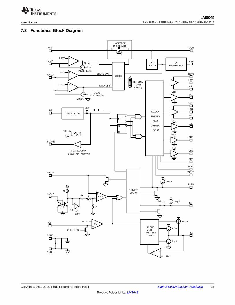
7.1 OverviewThe LM5045 PWM controller contains all of the features necessary to implement a full-bridge topology powerconverter using either current mode or voltage mode control. This device is intended to operate on the primaryside of an isolated DC-DC converter with input voltage up to 100 V. This highly integrated controller-driverprovides dual 2-A high-side and low-side gate drivers for the four external bridge MOSFETs plus control signalsfor secondary side synchronous rectifiers. External resistors program the leading and trailing edge dead-timebetween the main and synchronous rectifier control signals. Intelligent start-up of synchronous rectifier allowsturnon of the power converter into the prebias loads. Cycle-by-cycle current limit protects the power componentsfrom load transients while hiccup mode protection limits average power dissipation during extended overloadconditions. Additional features include programmable soft-start, soft-start of the synchronous rectifiers, and a 2-MHz capable oscillator with synchronization capability and thermal shutdown.
12 Submit Documentation Feedback Copyright © 2011–2015, Texas Instruments Incorporated
Product Folder Links: LM5045
HS1
HO1
BST1
LO1VCC
SR1
SR2
RD1
S
R
Q
TQ
Q
REF
REF
HS2
HO2
BST2
VCC
RD2
LO2
VOLTAGEREGULATOR
VCCUVLO
LOGIC
OSCILLATOR
DRIVERLOGIC
VIN
UVLO
OVP
RT
RAMP
SSSR
COMP
CS
SS
RES
AGND
PGND
REF
VCC
0.4V
1.25V
SHUTDOWN
STANDBY
UVLO HYSTERESIS
20 PA
1.25V
HYSTERESIS
CLK
PWM1V
5k
1:1
+
-
-
+
+
-
+
-
+
-
+
-
HICCUP MODE
TIMER and LOGIC
CS
SS
SLOPE
DELAY
TIMERS
AND
DRIVER
LOGIC
R
RSS
SS Buffer
0 PA
SSOFF
100 PA
20 PA
20 PA
30 PA
10 PA
5V
THERMALLIMIT
(160°C)
5VREFERENCE
20 PA
5 PA
1.0V
5V
SLOPECOMP
RAMP GENERATOR
0.75 V
CLK + LEB
LM5045www.ti.com SNVS699H –FEBRUARY 2011–REVISED JANUARY 2015
7.2 Functional Block Diagram
Copyright © 2011–2015, Texas Instruments Incorporated Submit Documentation Feedback 13
Product Folder Links: LM5045

LM5045SNVS699H –FEBRUARY 2011–REVISED JANUARY 2015 www.ti.com
7.3 Feature Description
7.3.1 High-Voltage Start-Up RegulatorThe LM5045 contains an internal high-voltage start-up regulator that allows the input pin (VIN) to be connecteddirectly to the supply voltage over a wide range from 14 V to 100 V. The input can withstand transients up to105 V. When the UVLO pin potential is greater than 0.4 V, the VCC regulator is enabled to charge an externalcapacitor connected to the VCC pin. The VCC regulator provides power to the voltage reference (REF) and thegate drivers (HO1/HO2 and LO1/LO2). When the voltage on the VCC pin exceeds its undervoltage (UV)threshold, the internal voltage reference (REF) reaches its regulation set point of 5 V and the UVLO voltage isgreater than 1.25 V, the soft-start capacitor is released and normal operation begins. The regulator output atVCC is internally current limited. The value of the VCC capacitor depends on the total system design, and itsstart-up characteristics. The recommended range of values for the VCC capacitor is 0.47 μF to 10 µF.
The internal power dissipation of the LM5045 can be reduced by powering VCC from an external supply. Theoutput voltage of the VCC regulator is initially regulated to 9.5 V. After the synchronous rectifiers are engaged(which is approximately when the output voltage in within regulation), the VCC voltage is reduced to 7.7 V. Intypical applications, an auxiliary transformer winding is connected through a diode to the VCC pin. This windingmust raise the VCC voltage above 8V to shut off the internal start-up regulator. Powering VCC from an auxiliarywinding improves efficiency while reducing the power dissipation of the controller. The VCC UV circuit will stillfunction in this mode, requiring that VCC never falls below its UV threshold during the start-up sequence. TheVCC regulator series pass transistor includes a diode between VCC and VIN that should not be forward biasedin normal operation. Therefore, the auxiliary VCC voltage should never exceed the VIN voltage.
An external DC bias voltage can be used instead of the internal regulator by connecting the external bias voltageto both the VCC and the VIN pins. This implementation is shown in the Application and Implementation section.The external bias must be greater than 10 V and less than the VCC maximum voltage rating of 14 V.
7.3.2 Line Undervoltage DetectorThe LM5045 contains a dual level undervoltage lockout (UVLO) circuit. When the UVLO pin voltage is below 0.4V, the controller is in a low current shutdown mode. When the UVLO pin voltage is greater than 0.4 V but lessthan 1.25 V, the controller is in standby mode. In standby mode the VCC and REF bias regulators are activewhile the controller outputs are disabled. When the VCC and REF outputs exceed their respective under-voltagethresholds and the UVLO pin voltage is greater than 1.25 V, the soft-start capacitor is released and the normaloperation begins. An external set-point voltage divider from VIN to GND can be used to set the minimumoperating voltage of the converter. The divider must be designed such that the voltage at the UVLO pin will begreater than 1.25 V when VIN enters the desired operating range. UVLO hysteresis is accomplished with aninternal 20 μA current sink that is switched on or off into the impedance of the set-point divider. When the UVLOthreshold is exceeded, the current sink is deactivated to quickly raise the voltage at the UVLO pin. When theUVLO pin voltage falls below the 1.25 V threshold, the current sink is enabled causing the voltage at the UVLOpin to quickly fall. The hysteresis of the 0.4 V shutdown comparator is internally fixed at 50 mV.
The UVLO pin can also be used to implement various remote enable / disable functions. Turning off theconverter by forcing the UVLO pin to standby condition (0.4 V < UVLO < 1.25 V) provides a controlled soft-stop.Refer to the Soft-Stop section for more details.
7.3.3 Overvoltage ProtectionAn external voltage divider can be used to set either an overvoltage or an overtemperature protection. During anOVP condition, the SS and SSSR capacitors are discharged and all the outputs are disabled. The divider mustbe designed such that the voltage at the OVP pin is greater than 1.25 V when overvoltage/temperature conditionexists. Hysteresis is accomplished with an internal 20 μA current source. When the OVP pin voltage exceeds1.25 V, the 20 μA current source is activated to quickly raise the voltage at the OVP pin. When the OVP pinvoltage falls below the 1.25 V threshold, the current source is deactivated causing the voltage at the OVP toquickly fall. Refer to the Application and Implementation section for more details.
7.3.4 ReferenceThe REF pin is the output of a 5-V linear regulator that can be used to bias an optocoupler transistor andexternal housekeeping circuits. The regulator output is internally current limited to 15 mA. The REF pin must belocally decoupled with a ceramic capacitor, the recommended range of values are from 0.1 μF to 10 μF
14 Submit Documentation Feedback Copyright © 2011–2015, Texas Instruments Incorporated
Product Folder Links: LM5045

RT =1
FOSC x 1 x 10⁻¹⁰
LM5045www.ti.com SNVS699H –FEBRUARY 2011–REVISED JANUARY 2015
Feature Description (continued)7.3.5 Oscillator, Sync InputThe LM5045 oscillator frequency is set by a resistor connected between the RT pin and AGND. The RT resistorshould be located very close to the device. To set a desired oscillator frequency (FOSC), the necessary value ofRT resistor can be calculated from the following equation:
(1)
For example, if the desired oscillator frequency is 400 kHz, that is, each phase (LO1 or LO2) at 200 kHz, thevalue of RT will be 25 kΩ. If the LM5045 is to be synchronized to an external clock, that signal must be coupledinto the RT pin through a 100 pF capacitor. The RT pin voltage is nominally regulated at 2.0 V and the externalpulse amplitude should lift the pin to between 3.5 V and 5.0 V on the low-to-high transition. The synchronizationpulse width should be between 15 and 200 ns. The RT resistor is always required, whether the oscillator is freerunning or externally synchronized and the SYNC frequency must be equal to, or greater than the frequency setby the RT resistor. When syncing to an external clock, it is recommended to add slope compensation byconnecting an appropriate resistor from the VCC pin to the CS pin. Also disable the SLOPE pin by grounding it.
7.3.6 Cycle-by-Cycle Current LimitThe CS pin is to be driven by a signal representative of the primary current of the transformer. If the voltage onthe CS pin exceeds 0.75 V, the current sense comparator immediately terminates the PWM cycle. A small RCfilter connected to the CS pin and located near the controller is recommended to suppress noise. An internal 18-Ω MOSFET discharges the external current sense filter capacitor at the conclusion of every cycle. The dischargeMOSFET remains on for an additional 40 ns after the start of a new PWM cycle to blank leading edge spikes.The current sense comparator is very fast and may respond to short duration noise pulses. Layout is critical forthe current sense filter and the sense resistor. The capacitor associated with CS filter must be placed very closeto the device and connected directly to the CS and AGND pins. If a current sense transformer is used, both theleads of the transformer secondary should be routed to the filter network, which should be located close to theIC. When designing with a current sense resistor, all of the noise sensitive low power ground connections shouldbe connected together near the AGND pin, and a single connection should be made to the power ground (senseresistor ground point).
7.3.7 Hiccup ModeThe LM5045 provides a current limit restart timer to disable the controller outputs and force a delayed restart(such as Hiccup mode) if a current limit condition is repeatedly sensed. The number of cycle-by-cycle currentlimit events required to trigger the restart is programmed by the external capacitor at the RES pin. During eachPWM cycle, the LM5045 either sources or sinks current from the RES capacitor. If current limit is detected, the 5μA current sink is disabled and a 30μA current source is enabled. If the RES voltage reaches the 1.0 Vthreshold, the following restart sequence occurs, as shown in Figure 10:• The SS and SSSR capacitors are fully discharged• The 30 μA current source is turned-off and the 10 μA current source is turned-on.• Once the voltage at the RES pin reaches 4.0 V the 10 μA current source is turned-off and a 5μA current sink
is turned-on, ramping the voltage on the RES capacitor down to 2.0 V.• Once RES capacitor reaches 2.0 V, threshold, the 10 μA current source is turned-on again. The RES
capacitor voltage is ramped between 4.0 V and 2.0 V eight times.• When the counter reaches eight, the RES pin voltage is pulled low and the soft-start capacitor is released to
begin a soft-start sequence. The SS capacitor voltage slowly increases. When the SS voltage reaches 1.0 V,the PWM comparator will produce the first narrow pulse.
• If the overload condition persists after restart, cycle-by-cycle current limiting will begin to increase the voltageon the RES capacitor again, repeating the hiccup mode sequence.
• If the overload condition no longer exists after restart, the RES pin will be held at ground by the 5 μA currentsink and the normal operation resumes.
The hiccup mode function can be completely disabled by connecting the RES pin to the AGND pin. In thisconfiguration the cycle-by-cycle protection will limit the maximum output current indefinitely, no hiccup restartsequences will occur.
Copyright © 2011–2015, Texas Instruments Incorporated Submit Documentation Feedback 15
Product Folder Links: LM5045

Hiccup Mode off-time
Soft-Start
Restart delay
1V
2V
4V
Count to Eight
1V
LM5045SNVS699H –FEBRUARY 2011–REVISED JANUARY 2015 www.ti.com
Feature Description (continued)
Figure 10. Hiccup Mode Delay and Soft-Start Timing Diagram
7.3.8 PWM ComparatorThe LM5045 pulse width modulator (PWM) comparator is a three input device, it compares the signal at theRAMP pin to the loop error signal or the soft-start, whichever is lower, to control the duty cycle. This comparatoris optimized for speed to achieve minimum controllable duty cycles. The loop error signal is received from theexternal feedback and isolation circuit in the form of a control current into the COMP pin. The COMP pin currentis internally mirrored by a matching pair of NPN transistors which sink current through a 5-kΩ resistor connectedto the 5-V reference. The resulting control voltage passes through a 1-V offset, followed by a 2:1 resistor dividerbefore being applied to the PWM comparator.
An optocoupler detector can be connected between the REF pin and the COMP pin. Because the COMP pin iscontrolled by a current input, the potential difference across the optocoupler detector is nearly constant. Thebandwidth limiting phase delay which is normally introduced by the significant capacitance of the optocoupler isthereby greatly reduced. Higher loop bandwidths can be realized because the bandwidth limiting pole associatedwith the optocoupler is now at a much higher frequency. The PWM comparator polarity is configured such thatwith no current flowing into the COMP pin, the controller produces maximum duty cycle.
7.3.9 Ramp PinThe voltage at the RAMP pin provides the modulation ramp for the PWM comparator. The PWM comparatorcompares the modulation ramp signal at the RAMP pin to the loop error signal to control the duty cycle. Themodulation ramp signal can be implemented either as a ramp proportional to the input voltage, known as feed-forward voltage mode control, or as a ramp proportional to the primary current, known as current mode control.The RAMP pin is reset by an internal MOSFET with an RDS(ON) of 5.5 Ω at the conclusion of each PWM cycle.The ability to configure the RAMP pin for either voltage mode or current mode allows the controller to beimplemented for the optimum control method depending upon the design constraints. Refer to the Applicationand Implementation section for more details on configuring the RAMP pin for feed-forward voltage mode controland peak current mode control.
7.3.10 Slope PinFor duty cycles greater than 50% (25% for each phase), peak current mode control is subject to sub-harmonicoscillation. Sub-harmonic oscillation is normally characterized by observing alternating wide and narrow dutycycles. This can be eliminated by adding an artificial ramp, known as slope compensation, to the modulatingsignal at the RAMP pin. The SLOPE pin provides a current source ramping from 0 to 100μA, at the frequency setby the RT resistor, for slope compensation. The ramping current source at the SLOPE pin can be used in severaldifferent ways to add slope compensation to the RAMP signal:• As shown in Figure 11(a), the SLOPE and RAMP pins can be connected together through an appropriate
resistor to the CS pin. This configuration will inject current sense signal plus slope compensation to the RAMP
16 Submit Documentation Feedback Copyright © 2011–2015, Texas Instruments Incorporated
Product Folder Links: LM5045

CSRFILTER
RCS
LM5045
RAMP
CLK + LEB
CLK CurrentSense
CFILTER
SLOPE
100 PA
0
CSRFILTER
RCS
LM5045
RAMP
CLK + LEB
CLK CurrentSense
CFILTER
SLOPE
100 PA
0
RSLOPE
(a) (b)
LM5045www.ti.com SNVS699H –FEBRUARY 2011–REVISED JANUARY 2015
Feature Description (continued)pin but CS pin will not see any slope compensation. Therefore, in this scheme slope compensation will notaffect the current limit.
• In a second configuration, as shown in Figure 11(b), the SLOPE, RAMP and CS pins can be tied together. Inthis configuration the ramping current source from the SLOPE pin will flow through the filter resistor and filtercapacitor, therefore both the CS pin and the RAMP pin will see the current sense signal plus the slopecompensation ramp. In this scheme, the current limit is compensated by the slope compensation and thecurrent limit onset point will vary.
If the slope compensation is not required for example, in feed-forward voltage mode control, the SLOPE pin mustbe connected to the AGND pin. When the RT pin is synched to an external clock, it is recommended to disablethe SLOPE pin and add slope compensation externally by connecting an appropriate resistor from the VCC pin tothe CS pin. Refer to the Application and Implementation section for more details.
A. Slope Compensation Configured for PWM Only (No Current Limit Slope)B. Slope Compensation Configured for PWM and Current Limit
Figure 11. Slope Compensation Configuration
7.3.11 Soft-StartThe soft-start circuit allows the power converter to gradually reach a steady state operating point, therebyreducing the start-up stresses and current surges. When bias is supplied to the LM5045, the SS capacitor isdischarged by an internal MOSFET. When the UVLO, VCC and REF pins reach their operating thresholds, theSS capacitor is released and is charged with a 20-µA current source. Once the SS pin voltage crosses the 1-Voffset, SS controls the duty cycle. The PWM comparator is a three input device; it compares the RAMP signalagainst the lower of the signals between the soft-start and the loop error signal. In a typical isolated application,as the secondary bias is established, the error amplifier on the secondary side soft-starts and establishes closed-loop control, steering the control away from the SS pin.
One method to shutdown the regulator is to ground the SS pin. This forces the internal PWM control signal toground, reducing the output duty cycle quickly to zero. Releasing the SS pin begins a soft-start cycle and normaloperation resumes. A second shutdown method is presented in the UVLO and OVP Voltage Divider Selectionsection.
7.3.12 Gate Driver OutputsThe LM5045 provides four gate drivers: two floating high-side gate drivers HO1 and HO2 and two groundreferenced low-side gate drivers LO1 and LO2. Each internal driver is capable of source 1.5-A peak and sinking2-A peak. Initially, the diagonal HO1 and LO2 are turned-on together, followed by an off-time when all the fourgate driver outputs are off. In the subsequent phase the diagonal HO2 and LO1 are turned on together followedby an off-time. The low-side gate drivers are powered directly by the VCC regulator. The HO1 and HO2 gate
Copyright © 2011–2015, Texas Instruments Incorporated Submit Documentation Feedback 17
Product Folder Links: LM5045

CLK
HO1,LO2
HO2,LO1Tonmax
T1
Tosc
T1
1 FOSC
TOSC =
T1 DRD1
DMAX =
- (T1)
2FOSC
)(
1FOSC
)(
LM5045SNVS699H –FEBRUARY 2011–REVISED JANUARY 2015 www.ti.com
Feature Description (continued)drivers are powered from a bootstrap capacitor connected between BST1/BST2 and HS1/HS2, respectively. Anexternal diode connected between VCC (anode pin) and BST (cathode pin) provides the high-side gate driverpower by charging the bootstrap capacitor from VCC when the corresponding switch node (HS1/HS2 pin) is low.When the high side MOSFET is turned on, BST1 rises to a peak voltage equal to VCC + VHS1 where VHS1 is theswitch node voltage.
The BST and VCC capacitors should be placed close to the pins of the LM5045 to minimize voltage transientsdue to parasitic inductances because the peak current sourced to the MOSFET gates can exceed 1.5 A. Therecommended value of the BST capacitor is 0.1 μF or greater. A low ESR / ESL capacitor, such as a surfacemount ceramic, should be used to prevent voltage droop during the HO transitions.
If the COMP pin is open circuit, the outputs will operate at maximum duty cycle. The maximum duty cycle foreach phase is limited by the dead-time set by the RD1 resistor. If the RD1 resistor is set to zero then themaximum duty cycle is slightly less than 50% due to the internally fixed dead-time. The internally fixed dead-timeis 30ns which does not vary with the operating frequency. The maximum duty cycle for each output can becalculated from the following equation:
where• T1 is the time set by the RD1 resistor• FOSC is the frequency of the oscillator (2)
For example, if the oscillator frequency is set at 400 kHz and the T1 time set by the RD1 resistor is 60 ns, theresulting DMAX will be equal to 0.488.
Figure 12. Timing Diagram Illustrating the Maximum Duty Cycle and Dead-Time Set by RD1
7.3.13 Synchronous Rectifier Control Outputs (SR1 and SR2)Synchronous rectification (SR) of the transformer secondary provides higher efficiency, especially for low outputvoltage converters, compared to the diode rectification. The reduction of rectifier forward voltage drop (0.5 V to1.5 V) to 10 mV to 200 mV VDS voltage for a MOSFET significantly reduces rectification losses. In a typicalapplication, the transformer secondary winding is center tapped, with the output power inductor in series with thecenter tap. The SR MOSFETs provide the ground path for the energized secondary winding and the inductorcurrent. From Figure 13 it can be seen that when the HO1/LO2 diagonal is turned ON, power transfer is enabledfrom the primary. During this period, the SR1 MOSFET is enabled and the SR2 MOSFET is turned-off. Thesecondary winding connected to the SR2 MOSFET drain is twice the voltage of the center tap at this time. At the
18 Submit Documentation Feedback Copyright © 2011–2015, Texas Instruments Incorporated
Product Folder Links: LM5045

HO1, LO2
SR2
HO2, LO1
SR1
T1 T2
T1 T2
RD(1,2) =T(1,2)3 pF
; For 20k < (1,2) < 100k
LM5045www.ti.com SNVS699H –FEBRUARY 2011–REVISED JANUARY 2015
Feature Description (continued)conclusion of the HO1/LO2 pulse, the inductor current continues to flow through the SR2 MOSFET body diode.Because the body diode causes more loss than the SR MOSFET, efficiency can be improved by minimizing theT2 period while maintaining sufficient timing margin over all conditions (component tolerances, etc.) to preventthe shoot-through current. When HO2/LO1 enables power transfer from the primary, the SR2 MOSFET isenabled and the SR1 MOSFET is off.
During the freewheeling period, the inductor current is almost equally shared between both the SR1 and SR2MOSFETs which effectively shorts the transformer secondary. The SR2 MOSFET is disabled before HO1/LO2 isturned-on. The SR2 MOSFET body diode continues to carry about the half inductor current until the primarypower raises the SR2 MOSFET drain voltage and reverse biases the body diode. Ideally, dead-time T1 would beset to the minimum time that allows the SR MOSFET to turn off before the SR MOSFET body diode startsconducting.
The SR drivers are powered by the REF regulator and each SR output is capable of sourcing 0.1 A and sinking0.4-A peak. The amplitude of the SR drivers is limited to 5 V. The 5-V SR signals enable the LM5045 to transferSR control across the isolation barrier either through a solid-state isolator or a pulse transformer. The actual gatesourcing and sinking currents for the synchronous MOSFETs are provided by the secondary-side bias and gatedrivers.
T1 and T2 can be programmed by connecting a resistor between RD1 and RD2 pins and AGND. It should benoted that while RD1 effects the maximum duty cycle, RD2 does not. The RD1 and RD2 resistors should belocated very close to the device. The formula for RD1 and RD2 resistors are given below:
(3)
If the desired dead-time for T1 is 60ns, then the RD1 will be 20 kΩ.
Figure 13. Synchronous Rectifier Timing Diagram
7.3.14 Soft-Start of the Synchronous RectifiersIn addition to the basic soft-start already described, the LM5045 contains a second soft-start function thatgradually turns on the synchronous rectifiers to their steady-state duty cycle. This function keeps thesynchronous rectifiers off during the basic soft-start allowing a linear start-up of the output voltage even into pre-biased loads. Then the SR output duty cycle is gradually increased to prevent output voltage disturbances due tothe difference in the voltage drop between the body diode and the channel resistance of the synchronousMOSFETs. Initially, when bias is supplied to the LM5045, the SSSR capacitor is discharged by an internalMOSFET. When the SS capacitor reaches a 2-V threshold and once it is established that COMP is in control ofthe duty cycle such as ICOMP < 800 µA, the SSSR discharge is released and SSSR capacitor begins chargingwith a 20-µA current source. Once the SSSR cap crosses the internal 1-V threshold, the LM5045 begins the soft-start of the synchronous FETs. The SR soft-start follows a leading edge modulation technique such as theleading edge of the SR pulse is soft-started as opposed trailing edge modulation of the primary FETs. As shownin the Figure 14(a), SR1 and SR2 are turned-on simultaneously with a narrow pulse-width during the
Copyright © 2011–2015, Texas Instruments Incorporated Submit Documentation Feedback 19
Product Folder Links: LM5045

HO1/LO2
HO2/LO1
SR1
SR2
Waveforms during soft-start Waveforms after soft-start
T1 T2
CLK
T1 T2FreewheelPower
Transfer
LM5045SNVS699H –FEBRUARY 2011–REVISED JANUARY 2015 www.ti.com
Feature Description (continued)freewheeling cycle. At the end of the freewheel cycle, that is, at the rising edge of the internal CLK, the SR FETin-phase with the next power transfer cycle is kept on while the SR FET out of phase with it is turned-off. The in-phase SR FET is kept on throughout the power transfer cycle and at the end of it, both the primary FETs and thein-phase SR FETs are turned-off together. The synchronous rectifier outputs can be disabled by grounding theSSSR pin.
A. Waveforms during Soft-StartB. Waveforms after Soft-Start
Figure 14. Waveforms
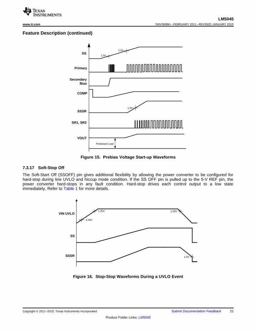
7.3.15 Prebias StartupA common requirement for power converters is to have a monotonic output voltage start-up into a prebiased loadsuch as a precharged output capacitor. In a prebiased load condition, if the synchronous rectifiers are engagedprematurely they will sink current from the precharged output capacitors resulting in an undesired output voltagedip. This condition is undesirable and could potentially damage the power converter. The LM5045 uses uniquecontrol circuitry to ensure intelligent turnon of the synchronous rectifiers such that the output has a monotonicstart-up. Initially, the SSSR capacitor is held at ground to disable the synchronous MOSFETs allowing the bodydiode to conduct. The synchronous rectifier soft-start is initiated once it is established the duty cycle is controlledby the COMP instead of the soft-start capacitor, that is, ICOMP < 800 µA and the voltage at the SS pin > 2 V. TheSSSR capacitor is then released and is charged by a 20-µA current source. Further, as shown in Figure 15, a 1-V offset on the SSSR pin is used to provide additional delay. This delay ensures the output voltage is inregulation avoiding any reverse current when the synchronous MOSFETs are engaged.
7.3.16 Soft-StopAs shown in Figure 16, if the UVLO pin voltage falls below the 1.25-V standby threshold, but above the 0.4-Vshutdown threshold, the SSSR capacitor is soft-stopped with a 60-µA current source (3 times the chargingcurrent). Once the SSSR pin reaches the 1.0-V threshold, both the SS and SSSR pins are immediatelydischarged to GND. Soft-stopping the power converter gradually winds down the energy in the output capacitorsand results in a monotonic decay of the output voltage. During the hiccup mode, the same sequence is executedexcept that the SSSR is discharged with a 120-µA current source (6 times the charging current). In case of anOVP, VCC UV, thermal limit or a VREF UV condition, the power converter hard-stops, whereby all of the controloutputs are driven to a low state immediately.
20 Submit Documentation Feedback Copyright © 2011–2015, Texas Instruments Incorporated
Product Folder Links: LM5045
VIN UVLO
SS
SSSR
1.25V 1.25V
0.45V
1.0V
SS
Primary
SR1, SR2
SSSR
1.0V
VOUT
1.0V
Prebiased Load
COMP
Secondary Bias
2.0V
LM5045www.ti.com SNVS699H –FEBRUARY 2011–REVISED JANUARY 2015
Feature Description (continued)
Figure 15. Prebias Voltage Start-up Waveforms
7.3.17 Soft-Stop OffThe Soft-Start Off (SSOFF) pin gives additional flexibility by allowing the power converter to be configured forhard-stop during line UVLO and hiccup mode condition. If the SS OFF pin is pulled up to the 5-V REF pin, thepower converter hard-stops in any fault condition. Hard-stop drives each control output to a low stateimmediately. Refer to Table 1 for more details.
Figure 16. Stop-Stop Waveforms During a UVLO Event
Copyright © 2011–2015, Texas Instruments Incorporated Submit Documentation Feedback 21
Product Folder Links: LM5045
LM5045SNVS699H –FEBRUARY 2011–REVISED JANUARY 2015 www.ti.com
Feature Description (continued)Table 1. Soft-Stop in Fault Conditions (1)
FAULT CONDITION SSSRUVLO Soft-Stop
(UVLO<1.25V) 3x the charging rateOVP Hard-Stop
(OVP>1.25V)Hiccup Soft-Stop
(CS>0.75 and RES>1V) 6x the charging rateVCC/VREF UV Hard-Stop
Internal Thermal Limit Hard-Stop
(1) Note: All the above conditions are valid with SSOFF pin tied to GND. If SSOFF=5V, the LM5045 hard-stops in all the conditions. The SSpin remains high in all the conditions until the SSSR pin reaches 1V.
7.3.18 Thermal ProtectionInternal thermal shutdown circuitry is provided to protect the integrated circuit in the event the maximum ratedjunction temperature is exceeded. When activated, typically at 160°C, the controller is forced into a shutdownstate with the output drivers, the bias regulators (VCC and REF) disabled. This helps to prevent catastrophicfailures from accidental device overheating. During thermal shutdown, the SS and SSSR capacitors are fullydischarged and the controller follows a normal start-up sequence after the junction temperature falls to theoperating level (140°C).
7.4 Device Functional Modes
7.4.1 Control Method SelectionThe LM5045 is a versatile PWM control IC that can be configured for either current mode control or voltagemode control. The choice of the control method usually depends upon the designer preference. The followingmust be taken into consideration while selecting the control method. Current mode control can inherently balanceflux in both phases of the full-bridge topology. The full-bridge topology, like other double ended topologies, issusceptible to the transformer core saturation. Any asymmetry in the volt-second product applied between thetwo alternating phases results in flux imbalance that causes a dc buildup in the transformer. This continual dcbuildup may eventually push the transformer into saturation. The volt-second asymmetry can be corrected byemploying current mode control. In current mode control, a signal representative of the primary current iscompared against an error signal to control the duty cycle. In steady-state, this results in each phase beingterminated at the same peak current by adjusting the pulse-width and thus applying equal volt-seconds to boththe phases.
Current mode control can be susceptible to noise and sub-harmonic oscillation, while voltage mode controlemploys a larger ramp for PWM and is usually less susceptible. Voltage-mode control with input line feed-forward also has excellent line transient response. When configuring for voltage mode control, a dc blockingcapacitor can be placed in series with the primary winding of the power transformer to avoid any flux imbalancethat may cause transformer core saturation.
7.4.2 Voltage Mode Control Using the LM5045To configure the LM5045 for voltage mode control, an external resistor (RFF) and capacitor (CFF) connected toVIN, AGND, and the RAMP pins is required to create a saw-tooth modulation ramp signal shown in Figure 17.The slope of the signal at RAMP will vary in proportion to the input line voltage. The varying slope provides linefeed-forward information necessary to improve line transient response with voltage mode control. With a constanterror signal, the on-time (TON) varies inversely with the input voltage (VIN) to stabilize the Volt- Second productof the transformer primary. Using a line feed-forward ramp for PWM control requires very little change in thevoltage regulation loop to compensate for changes in input voltage, as compared to a fixed slope oscillator ramp.Furthermore, voltage mode control is less susceptible to noise and does not require leading edge filtering.Therefore, it is a good choice for wide input range power converters. Voltage mode control requires a Type-IIIcompensation network, due to the complex-conjugate poles of the L-C output filter.
22 Submit Documentation Feedback Copyright © 2011–2015, Texas Instruments Incorporated
Product Folder Links: LM5045

RFF =-1
VRAMP
VINMIN(1-FOSC x CFF x In )
VIN
RFF
CFF
LM5045
SLOPE PROPORTIONAL
TO VIN
COMP
Gate Drive1V
CLK
VINR
R
5V
5k
1:1
RAMP
LM5045www.ti.com SNVS699H –FEBRUARY 2011–REVISED JANUARY 2015
Device Functional Modes (continued)
Figure 17. Feed-Forward Voltage Mode Configuration
The recommended capacitor value range for CFF is from 100 pF to 1800 pF. Referring to Figure 17, it can beseen that CFF value must be small enough to be discharged with in the clock pulse-width which is typically within50ns. The RDS(ON) of the internal discharge FET is 5.5 Ω.
The value of RFF required can be calculated from
(4)
For example, assuming a VRAMP of 1.5 V (a good compromise of signal range and noise immunity), at VINMIN of36 V (oscillator frequency of 400 kHz and CFF = 470 pF results in a value for RFF of 125 kΩ.
7.4.3 Current Mode Control Using the LM5045The LM5045 can be configured for current mode control by applying a signal proportional to the primary currentto the RAMP pin. One way to achieve this is shown in Figure 18. The primary current can be sensed using acurrent transformer or sense resistor, the resulting signal is filtered and applied to the RAMP pin through aresistor used for slope compensation. It can be seen that the signal applied to the RAMP pin consists of theprimary current information from the CS pin plus an additional ramp for slope compensation, added by theresistor RSLOPE.
The current sense resistor is selected such that during over current condition, the voltage across the currentsense resistor is above the minimum CS threshold of 728 mV.
In general, the amount of slope compensation required to avoid sub-harmonic oscillation is equal to at least one-half the down-slope of the output inductor current, transformed to the primary. To mitigate sub-harmonicoscillation after one switching period, the slope compensation must be equal to one times the down slope of thefilter inductor current transposed to primary. This is known as deadbeat control. The slope compensation resistorrequired to implement dead-beat control can be calculated as follows:
where• NTR is the turns-ratio with respect to the secondary (5)
For example, for a 3.3 V output converter with a turns-ratio between primary and secondary of 9:1, an outputfilter inductance (LFILTER) of 800 nH and a current sense resistor (RSENSE) of 150 mΩ, RSLOPE of 1.67 kΩ willsuffice.
Copyright © 2011–2015, Texas Instruments Incorporated Submit Documentation Feedback 23
Product Folder Links: LM5045

CSRFILTER
RCS
LM5045
RAMP
CLK + LEB
CLK CurrentSense
CFILTER
SLOPE
100 PA
0
RSLOPE
LM5045SNVS699H –FEBRUARY 2011–REVISED JANUARY 2015 www.ti.com
Device Functional Modes (continued)
Figure 18. Current Mode Configuration
24 Submit Documentation Feedback Copyright © 2011–2015, Texas Instruments Incorporated
Product Folder Links: LM5045
LM5045www.ti.com SNVS699H –FEBRUARY 2011–REVISED JANUARY 2015
8 Application and Implementation
NOTEInformation in the following applications sections is not part of the TI componentspecification, and TI does not warrant its accuracy or completeness. TI’s customers areresponsible for determining suitability of components for their purposes. Customers shouldvalidate and test their design implementation to confirm system functionality.
8.1 Application InformationThe LM5045 is a highly integrated PWM controller that contains all of the features necessary for implementingfull-bridge topology power converters using either current mode or voltage mode control. The device targets DC-DC converter applications with input voltages of up to 100 Vdc and output power in the range 100 W to 1 kW.
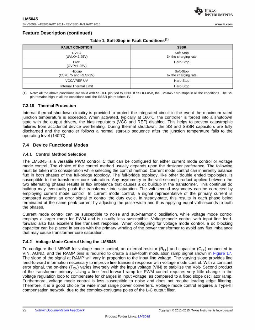
8.2 Typical ApplicationThe following schematic shows an example of a 100W full-bridge converter controlled by LM5045. The operatinginput voltage range is 36 V to 75 V, and the output voltage is 3.3 V. The output current capability is 30 A. Theconverter is configured for current mode control with external slope compensation. An auxiliary winding is used toraise the VCC voltage to reduce the controller power dissipation.
Figure 19. Evaluation Board Schematic
8.2.1 Design Requirements
PARAMETERS VALUEInput operating range 36 V to 75 V
Output voltage 3.3 VMeasured efficiency at 48 V 92% at 30A
Frequency of operation 420 kHzBoard size 2.28 x 1.45 x 0.5 inches
Copyright © 2011–2015, Texas Instruments Incorporated Submit Documentation Feedback 25
Product Folder Links: LM5045

VPWR VIN VCC
10V - 16V (from aux winding)
LM504511V
0.1 PF
50
LM5045
VIN
VPWR
LM5045SNVS699H –FEBRUARY 2011–REVISED JANUARY 2015 www.ti.com
Typical Application (continued)PARAMETERS VALUELoad Regulation 0.2%Line Regulation 0.1%
Line UVLO 34V/32V on/offHiccup Mode Current Limit
8.2.2 Detailed Design Procedure
8.2.2.1 VIN and VCC
The voltage applied to the VIN pin, which may be the same as the system voltage applied to the powertransformer’s primary (VPWR), can vary in the range of the 14 to 100 V. It is recommended that the filter shown inFigure 20 be used to suppress the transients that may occur at the input supply. This is particularly importantwhen VIN is operated close to the maximum operating rating of the LM5045. The current into VIN dependsprimarily on the operating current of the LM5045, the switching frequency, and any external loads on the VCCpin, that typically include the gate capacitances of the power MOSFETs. In typical applications, an auxiliarytransformer winding is connected through a diode to the VCC pin. This pin must raise VCC voltage above 8 V toshut off the internal start-up regulator.
After the outputs are enabled and the external VCC supply voltage has begun supplying power to the IC, thecurrent into the VIN pin drops below 1mA. VIN should remain at a voltage equal to or above the VCC voltage toavoid reverse current through the internal body diode of the internal VCC regulator.
8.2.2.2 For Applications With > 100 VINFor applications where the system input voltage exceeds 100 V, VIN can be powered from an external start-upregulator as shown in Figure 21. In this configuration, the VIN and VCC pins should be connected together. Thevoltage at the VCC and VIN pins must be greater than 10 V (> Max VCC reference voltage) yet not exceed 16 V.To enable operation the VCC voltage must be raised above 10 V. The voltage at the VCC pin must not exceed16 V. The voltage source at the right side of Figure 21 is typically derived from the power stage, and becomesactive once the LM5045’s outputs are active.
Figure 20. Input Transient Protection
Figure 21. Start-Up Regulator For VPWR > 100 V
26 Submit Documentation Feedback Copyright © 2011–2015, Texas Instruments Incorporated
Product Folder Links: LM5045

UVLO
LM5045
1.25V
20 PA
SHUTDOWN
VPWR
R1
R2
STANDBY
0.4V
R2 =1.25V x R1
VPWR -1.25V + (20 PA x R1)
VHYS
20 PAR1 =
R2 =1.25V x R1
VPWR-OFF -1.25V - (20 PA x R1)
R1 =VHYS
20 PA
LM5045www.ti.com SNVS699H –FEBRUARY 2011–REVISED JANUARY 2015
8.2.2.3 UVLO and OVP Voltage Divider SelectionTwo dedicated comparators connected to the UVLO and OVP pins are used to detect undervoltage andovervoltage conditions. The threshold values of both these comparators are set at 1.25 V. The two functions canbe programmed independently with two separate voltage dividers from VIN to AGND as shown in Figure 22 andFigure 23, or with a three-resistor divider as shown in Figure 24. Independent UVLO and OVP pins providegreater flexibility for the user to select the operational voltage range of the system. When the UVLO pin voltage isbelow 0.4 V, the controller is in a low current shutdown mode. For a UVLO pin voltage greater than 0.4 V butless than 1.25 V the controller is in standby mode. Once the UVLO pin voltage is greater than 1.25 V, thecontroller is fully enabled. Two external resistors can be used to program the minimum operational voltage for thepower converter as shown in Figure 22. When the UVLO pin voltage falls below the 1.25 V threshold, an internal20 µA current sink is enabled to lower the voltage at the UVLO pin, thus providing threshold hysteresis.Resistance values for R1 and R2 can be determined from the following equations:
where• VPWR is the desired turnon voltage• VHYS is the desired UVLO hysteresis at VPWR (6)
For example, if the LM5045 is to be enabled when VPWR reaches 33 V, and disabled when VPWR is decreased to31 V, R1 should be 100 kΩ, and R2 should be 4.2 kΩ. The voltage at the UVLO pin should not exceed 7 V at anytime.
Two external resistors can be used to program the maximum operational voltage for the power converter asshown in Figure 23. When the OVP pin voltage rises above the 1.25 V threshold, an internal 20-µA currentsource is enabled to raise the voltage at the OVP pin, thus providing threshold hysteresis. Resistance values forR1 and R2 can be determined from the following equations:
(7)
If the LM5045 is to be disabled when VPWR-OFF reaches 80 V and enabled when it is decreased to 78 V. R1should be 100 kΩ, and R2 should be 1.5 kΩ. The voltage at the OVP pin should not exceed 7 V at any time.
Figure 22. Basic UVLO Configuration
Copyright © 2011–2015, Texas Instruments Incorporated Submit Documentation Feedback 27
Product Folder Links: LM5045

1.25V
20 PA
0.4VSHUTDOWN
OVP
1.25VSTANDBY
VPWR
5V
R1
R2
R3
LM5045STANDBYUVLO
20 PA
OVP
LM5045
1.25V
20 PA
STANDBY
VPWR
5V
R1
R2
LM5045SNVS699H –FEBRUARY 2011–REVISED JANUARY 2015 www.ti.com
Figure 23. Basic OVP Configuration
Figure 24. UVLO/OVP Divider
The UVLO and OVP can also be set together using a 3 resistor divider ladder as shown in Figure 24. R1 iscalculated as explained in the basic UVLO divider selection. Using the same values, as in the above twoexamples, for the UVLO and OVP set points, R1 and R3 remain the same at 100 kΩ and 1.5 kΩ. The R2 is 2.7kΩ obtained by subtracting R3 from 4.2 kΩ.
Remote configuration of the controller’s operational modes can be accomplished with open drain device(s)connected to the UVLO pin as shown in Figure 25.
Figure 26 shows an application of the OVP comparator for Remote Thermal Protection using a thermistor (ormultiple thermistors) which may be located near the main heat sources of the power converter. The negativetemperature coefficient (NTC) thermistor is nearly logarithmic, and in this example a 100 kΩ thermistor with the βmaterial constant of 4500 Kelvin changes to approximately 2 kΩ at 130ºC. Setting R1 to one-third of thisresistance (665 Ω) establishes 130ºC as the desired trip point (for VREF = 5 V). In a temperature band from20ºC below to 20ºC above the OVP threshold, the voltage divider is nearly linear with 25mV per ºC sensitivity.
R2 provides temperature hysteresis by raising the OVP comparator input by R2 x 20µA. For example, if a 22kΩresistor is selected for R2, then the OVP pin voltage will increase by 22 kΩ x 20 µA = 506 mV. The NTCtemperature must therefore fall by 506 mV / 25 mV per ºC = 20ºC before the LM5045 switches from standbymode to the normal mode.
28 Submit Documentation Feedback Copyright © 2011–2015, Texas Instruments Incorporated
Product Folder Links: LM5045

Q1
Q2
Q3
Q4
VPWR
NP
NS1
NS2
RF
CFRCS
CS
LM5045
VIN
AGND
NTCTHERMISTOR
OVP
LM5045
1.25V
20 PA
STANDBY
VPWR5V
R1
R2
T
UVLO
LM5045
1.25V
20 PA
SHUTDOWN
VPWR
R1
STANDBY
0.4V
STANDBY SHUTDOWN R2
LM5045www.ti.com SNVS699H –FEBRUARY 2011–REVISED JANUARY 2015
Figure 25. Remote Standby and Disable Control
Figure 26. Remote Thermal Protection
8.2.2.4 Current SenseThe CS pin receives an input signal representative of its transformer’s primary current, either from a currentsense transformer or from a resistor located at the junction of source pin of the primary switches, as shown inFigure 27 and Figure 28, respectively. In both the cases, the filter components RF and CF should be located asclose to the IC as possible, and the ground connection from the current sense transformer, or RSENSE should bea dedicated trace to the appropriate GND pin. Please refer to the Layout section for more layout tips.
The current sense components must provide a signal > 710 mV at the CS pin during an over-load event. Oncethe voltage on the CS pin crosses the current limit threshold, the current sense comparator terminates the PWMpulse and starts to charge the RES pin. Depending on the configuration of the RES pin, the LM5045 willeventually initiate a hiccup mode restart or be in continuous current limit.
Figure 27. Transformer Current Sense
Copyright © 2011–2015, Texas Instruments Incorporated Submit Documentation Feedback 29
Product Folder Links: LM5045

Hiccup Mode off-time
Soft-Start
Restart delay
1V
2V
4V
Count to Eight
1V
THICCUP =5 µA
CRES x (2.0Vx8)10 µA
CRES x ((2.0Vx8) + 1.0V)+
TCS =CRES x 1.0V
30 PA
Q1
Q2
Q3
Q4
NP
CS
LM5045 RFCF
RCS
VIN
AGND
LM5045SNVS699H –FEBRUARY 2011–REVISED JANUARY 2015 www.ti.com
Figure 28. Resistor Current Sense
8.2.2.5 Hiccup Mode Current Limit RestartThe operation of the hiccup mode restart circuit is explained in the section. During a continuous current limitcondition, the RES pin is charged with 30 µA current source. The restart delay time required to reach the 1.0 Vthreshold is given by:
(8)
This establishes the time allowed before the IC initiates a hiccup restart sequence. For example, if the CRES =0.01 µF, the time TCS as noted in Figure 29 below is 334 µs. Once the RES pin reaches 1.0 V, the 30 µAcurrent source is turned-off and a 10 µA current source is turned-on during the ramp up to 4 V and a 5 µA isturned on during the ramp down to 2 V. The hiccup mode off-time is given by:
(9)
With a CRES = 0.01 µF, the hiccup time is 49 ms. Once the hiccup time is finished, the RES pin is pulled low andthe SS pin is released allowing a soft-start sequence to commence. Once the SS pin reaches 1 V, the PWMpulses will commence. The hiccup mode provides a cool-down period for the power converter in the event of asustained overload condition thereby lowering the average input current and temperature of the powercomponents during such an event.
Figure 29. Hiccup Mode Delay and Soft-Start Timing Diagram
30 Submit Documentation Feedback Copyright © 2011–2015, Texas Instruments Incorporated
Product Folder Links: LM5045

LO1
PGND
VCC
BST1
HO1
HS1
VINLM5045
Q1
D1
LM5045www.ti.com SNVS699H –FEBRUARY 2011–REVISED JANUARY 2015
8.2.2.6 Augmenting the Gate Drive StrengthThe LM5045 includes powerful 2-A integrated gate drivers. However, in certain high-power applications (> 500W), it might be necessary to augment the strength of the internal gate driver to achieve higher efficiency andbetter thermal performance. In high power applications, typically, the I2xR loss in the primary MOSFETs issignificantly higher than the switching loss. To minimize the I2xR loss, either the primary MOSFETs are paralleledor MOSFETs with low RDS (on) are employed. Both these scenarios increase the total gate charge to be driven bythe controller IC. An increase in the gate charge increases the FET transition time and hence increases theswitching losses. Therefore, to keep the total losses within a manageable limit the transition time must bereduced.
Generally, during the Miller capacitance charge/discharge the total available driver current is lower during theturnoff process than during the turnon process and often it is enough to speed-up the turnoff time to achieve theefficiency and thermal goals. This can be achieved simply by employing a PNP device, as shown in Figure 30,from gate to source of the power FET. During the turnon process, when the LO1 goes high, the current issourced through the diode D1 and the BJT Q1 provides the path for the turnoff current. Q1 should be located asclose to the power FET as possible so that the turnoff current has the shortest possible path to the ground anddoes not have to pass through the controller.
Figure 30. Circuit to Speed-Up the Turnoff Process
Depending on the gate charge characteristics of the primary FET, if it is required to speed up both the turnon andthe turnoff time, a bipolar totem pole structure as shown in Figure 31 can be used. When LO1 goes high, thegate to source current is sourced through the NPN transistor Q1 and similar to the circuit shown in Figure 30when LO1 goes low, the PNP transistor Q2 expedites the turnoff process.
Copyright © 2011–2015, Texas Instruments Incorporated Submit Documentation Feedback 31
Product Folder Links: LM5045

LO1
PGND
LM5112
LM5112
VCC
BST1
HO1
HS1
VINLM5045
LO1
PGND
VCC
BST1
HO1
HS1
VINLM5045
Q1
Q2
LM5045SNVS699H –FEBRUARY 2011–REVISED JANUARY 2015 www.ti.com
Figure 31. Bipolar Totem Pole Arrangement
Alternatively, a low-side gate driver such as LM5112 can be used instead of the discrete totem pole. TheLM5112 comes in a small package with a 3A source and a 7A sink capability. While driving the high-side FET,the HS1 acts as a local ground and the boot capacitor between the BST and HS pins acts as VCC.
Figure 32. Using a Low-Side Gate Driver to Augment Gate Drive Strength
32 Submit Documentation Feedback Copyright © 2011–2015, Texas Instruments Incorporated
Product Folder Links: LM5045

LM5045www.ti.com SNVS699H –FEBRUARY 2011–REVISED JANUARY 2015
8.2.3 Application Curve
Figure 33. Application Board Efficiency
Copyright © 2011–2015, Texas Instruments Incorporated Submit Documentation Feedback 33
Product Folder Links: LM5045

LM5045SNVS699H –FEBRUARY 2011–REVISED JANUARY 2015 www.ti.com
9 Power Supply RecommendationsThe LM5045 can be used to control power levels up to 1 kW. Therefore the current levels can be considerable.Care should be taken that components with the correct current rating are chosen. This would include magneticcomponents, power MOSFETS and diodes, connectors and wire sizes. Input and output capacitors should havethe correct ripple current rating. The use of a multilayer PCB is recommended with a copper area chosen toensure the LM5045 is operating below its maximum junction temperature.
Full power loading should never be attempted with providing with providing adequate cooling.
10 Layout
10.1 Layout GuidelinesThe LM5045 current sense and PWM comparators are very fast and respond to short duration noise pulses. Thecomponents at the CS, COMP, SLOPE, RAMP, SS, SSSR, RES, UVLO, OVP, RD1, RD2, and RT pins shouldbe physically close as possible to the IC, thereby minimizing noise pickup on the PC board trace inductance.Eliminating or minimizing via’s in these critical connections are essential. Layout consideration is critical for thecurrent sense filter. If a current sense transformer is used, both leads of the transformer secondary should berouted to the sense filter components and to the IC pins. The ground side of the transformer should beconnected via a dedicated PC board trace to the AGND pin, rather than through the ground plane. If the currentsense circuit employs a sense resistor in the drive transistor source, low inductance resistors should be used. Inthis case, all the noise sensitive, low-current ground trace should be connected in common near the IC, and thena single connection made to the power ground (sense resistor ground point).
The gate drive outputs of the LM5045 should have short, direct paths to the power MOSFETs to minimizeinductance in the PC board. The boot-strap capacitors required for the high side gate drivers should be locatedvery close to the IC and connected directly to the BST and HS pins. The VCC and REF capacitors should alsobe placed close to their respective pins with short trace inductance. Low ESR and ESL ceramic capacitors arerecommended for the boot-strap, VCC and the REF capacitors. The two ground pins (AGND, PGND) must beconnected together directly underneath the IC with a short, direct connection, to avoid jitter due to relative groundbounce.
34 Submit Documentation Feedback Copyright © 2011–2015, Texas Instruments Incorporated
Product Folder Links: LM5045

RTSSSR
VIN
HS1
HO1
BST1
SR1
LO1
PGND
VCC
LO2
SR2
BST2
HO2
HS2
SS OFF
UVLO
OVP
RAMP
CS
SLOPE
COMP
REF
RT
AGND
RD1
RD2
RES
SS
SSSR
RD1 RD2SSRES
C_FILTER
RAMP
R_FILTER
To Current SensingNetwork
To Voltage FeedbackNetwork
LM5045www.ti.com SNVS699H –FEBRUARY 2011–REVISED JANUARY 2015
10.2 Layout Example
Figure 34. Layout of Components Around RAMP, CS, SLOPE, COMP, RT, RD1, RD2, RES, SS, and SSR
Copyright © 2011–2015, Texas Instruments Incorporated Submit Documentation Feedback 35
Product Folder Links: LM5045

R1
R2
C1
INPUT DC VOLTAGE
R3
C2
C3
C4
C4
VIN
HS1
HO1
BST1
SR1
LO1
PGND
VCC
LO2
SR2
BST2
HO2
HS2
SS OFF
UVLO
OVP
RAMP
CS
SLOPE
COMP
REF
RT
AGND
RD1
RD2
RES
SS
SSSR
LM5045SNVS699H –FEBRUARY 2011–REVISED JANUARY 2015 www.ti.com
Layout Example (continued)
Figure 35. Layout of Components Around VIN, VCC, AGND, PGND UVLO, OVP, REF, BST1, BST2, HS1,and HS2
36 Submit Documentation Feedback Copyright © 2011–2015, Texas Instruments Incorporated
Product Folder Links: LM5045

LM5045www.ti.com SNVS699H –FEBRUARY 2011–REVISED JANUARY 2015
11 Device and Documentation Support
11.1 TrademarksPowerPAD is a trademark of Texas Instruments.All other trademarks are the property of their respective owners.
11.2 Electrostatic Discharge CautionThese devices have limited built-in ESD protection. The leads should be shorted together or the device placed in conductive foamduring storage or handling to prevent electrostatic damage to the MOS gates.
11.3 GlossarySLYZ022 — TI Glossary.
This glossary lists and explains terms, acronyms, and definitions.
12 Mechanical, Packaging, and Orderable InformationThe following pages include mechanical, packaging, and orderable information. This information is the mostcurrent data available for the designated devices. This data is subject to change without notice and revision ofthis document. For browser-based versions of this data sheet, refer to the left-hand navigation.
Copyright © 2011–2015, Texas Instruments Incorporated Submit Documentation Feedback 37
Product Folder Links: LM5045
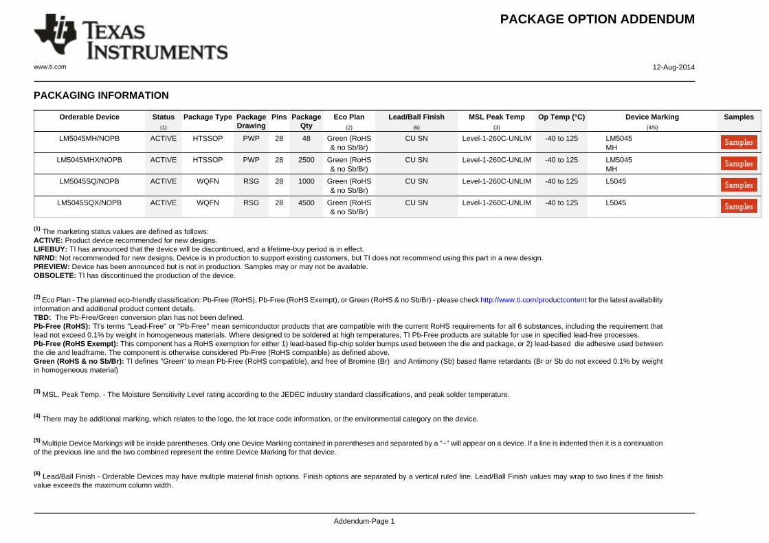
PACKAGE OPTION ADDENDUM
www.ti.com 12-Aug-2014
Addendum-Page 1
PACKAGING INFORMATION
Orderable Device Status(1)
Package Type PackageDrawing
Pins PackageQty
Eco Plan(2)
Lead/Ball Finish(6)
MSL Peak Temp(3)
Op Temp (°C) Device Marking(4/5)
Samples
LM5045MH/NOPB ACTIVE HTSSOP PWP 28 48 Green (RoHS& no Sb/Br)
CU SN Level-1-260C-UNLIM -40 to 125 LM5045MH
LM5045MHX/NOPB ACTIVE HTSSOP PWP 28 2500 Green (RoHS& no Sb/Br)
CU SN Level-1-260C-UNLIM -40 to 125 LM5045MH
LM5045SQ/NOPB ACTIVE WQFN RSG 28 1000 Green (RoHS& no Sb/Br)
CU SN Level-1-260C-UNLIM -40 to 125 L5045
LM5045SQX/NOPB ACTIVE WQFN RSG 28 4500 Green (RoHS& no Sb/Br)
CU SN Level-1-260C-UNLIM -40 to 125 L5045
(1) The marketing status values are defined as follows:ACTIVE: Product device recommended for new designs.LIFEBUY: TI has announced that the device will be discontinued, and a lifetime-buy period is in effect.NRND: Not recommended for new designs. Device is in production to support existing customers, but TI does not recommend using this part in a new design.PREVIEW: Device has been announced but is not in production. Samples may or may not be available.OBSOLETE: TI has discontinued the production of the device.
(2) Eco Plan - The planned eco-friendly classification: Pb-Free (RoHS), Pb-Free (RoHS Exempt), or Green (RoHS & no Sb/Br) - please check http://www.ti.com/productcontent for the latest availabilityinformation and additional product content details.TBD: The Pb-Free/Green conversion plan has not been defined.Pb-Free (RoHS): TI's terms "Lead-Free" or "Pb-Free" mean semiconductor products that are compatible with the current RoHS requirements for all 6 substances, including the requirement thatlead not exceed 0.1% by weight in homogeneous materials. Where designed to be soldered at high temperatures, TI Pb-Free products are suitable for use in specified lead-free processes.Pb-Free (RoHS Exempt): This component has a RoHS exemption for either 1) lead-based flip-chip solder bumps used between the die and package, or 2) lead-based die adhesive used betweenthe die and leadframe. The component is otherwise considered Pb-Free (RoHS compatible) as defined above.Green (RoHS & no Sb/Br): TI defines "Green" to mean Pb-Free (RoHS compatible), and free of Bromine (Br) and Antimony (Sb) based flame retardants (Br or Sb do not exceed 0.1% by weightin homogeneous material)
(3) MSL, Peak Temp. - The Moisture Sensitivity Level rating according to the JEDEC industry standard classifications, and peak solder temperature.
(4) There may be additional marking, which relates to the logo, the lot trace code information, or the environmental category on the device.
(5) Multiple Device Markings will be inside parentheses. Only one Device Marking contained in parentheses and separated by a "~" will appear on a device. If a line is indented then it is a continuationof the previous line and the two combined represent the entire Device Marking for that device.
(6) Lead/Ball Finish - Orderable Devices may have multiple material finish options. Finish options are separated by a vertical ruled line. Lead/Ball Finish values may wrap to two lines if the finishvalue exceeds the maximum column width.

PACKAGE OPTION ADDENDUM
www.ti.com 12-Aug-2014
Addendum-Page 2
Important Information and Disclaimer:The information provided on this page represents TI's knowledge and belief as of the date that it is provided. TI bases its knowledge and belief on informationprovided by third parties, and makes no representation or warranty as to the accuracy of such information. Efforts are underway to better integrate information from third parties. TI has taken andcontinues to take reasonable steps to provide representative and accurate information but may not have conducted destructive testing or chemical analysis on incoming materials and chemicals.TI and TI suppliers consider certain information to be proprietary, and thus CAS numbers and other limited information may not be available for release.
In no event shall TI's liability arising out of such information exceed the total purchase price of the TI part(s) at issue in this document sold by TI to Customer on an annual basis.
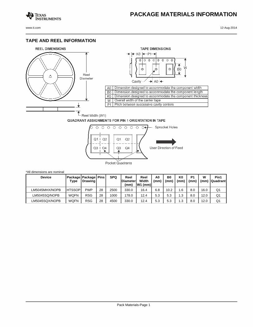
TAPE AND REEL INFORMATION
*All dimensions are nominal
Device PackageType
PackageDrawing
Pins SPQ ReelDiameter
(mm)
ReelWidth
W1 (mm)
A0(mm)
B0(mm)
K0(mm)
P1(mm)
W(mm)
Pin1Quadrant
LM5045MHX/NOPB HTSSOP PWP 28 2500 330.0 16.4 6.8 10.2 1.6 8.0 16.0 Q1
LM5045SQ/NOPB WQFN RSG 28 1000 178.0 12.4 5.3 5.3 1.3 8.0 12.0 Q1
LM5045SQX/NOPB WQFN RSG 28 4500 330.0 12.4 5.3 5.3 1.3 8.0 12.0 Q1
PACKAGE MATERIALS INFORMATION
www.ti.com 12-Aug-2014
Pack Materials-Page 1

*All dimensions are nominal
Device Package Type Package Drawing Pins SPQ Length (mm) Width (mm) Height (mm)
LM5045MHX/NOPB HTSSOP PWP 28 2500 367.0 367.0 35.0
LM5045SQ/NOPB WQFN RSG 28 1000 210.0 185.0 35.0
LM5045SQX/NOPB WQFN RSG 28 4500 367.0 367.0 35.0
PACKAGE MATERIALS INFORMATION
www.ti.com 12-Aug-2014
Pack Materials-Page 2

www.ti.com
PACKAGE OUTLINE
C
TYP6.66.2
1.1 MAX
26X 0.65
28X 0.300.19
2X8.45
TYP0.200.09
0 - 80.100.02
5.655.25
3.152.75
(1)
0.25GAGE PLANE
0.70.5
A
NOTE 3
9.89.6
BNOTE 4
4.54.3
4214870/A 10/2014
PowerPAD - 1.1 mm max heightPWP0028APLASTIC SMALL OUTLINE
NOTES: 1. All linear dimensions are in millimeters. Any dimensions in parenthesis are for reference only. Dimensioning and tolerancing per ASME Y14.5M. 2. This drawing is subject to change without notice. 3. This dimension does not include mold flash, protrusions, or gate burrs. Mold flash, protrusions, or gate burrs shall not exceed 0.15 mm, per side. 4. This dimension does not include interlead flash. Interlead flash shall not exceed 0.25 mm, per side.5. Reference JEDEC registration MO-153, variation AET.
PowerPAD is a trademark of Texas Instruments.
TM
128
0.1 C A B
1514
PIN 1 IDAREA
SEATING PLANE
0.1 C
SEE DETAIL A
DETAIL ATYPICAL
SCALE 1.800
THERMALPAD
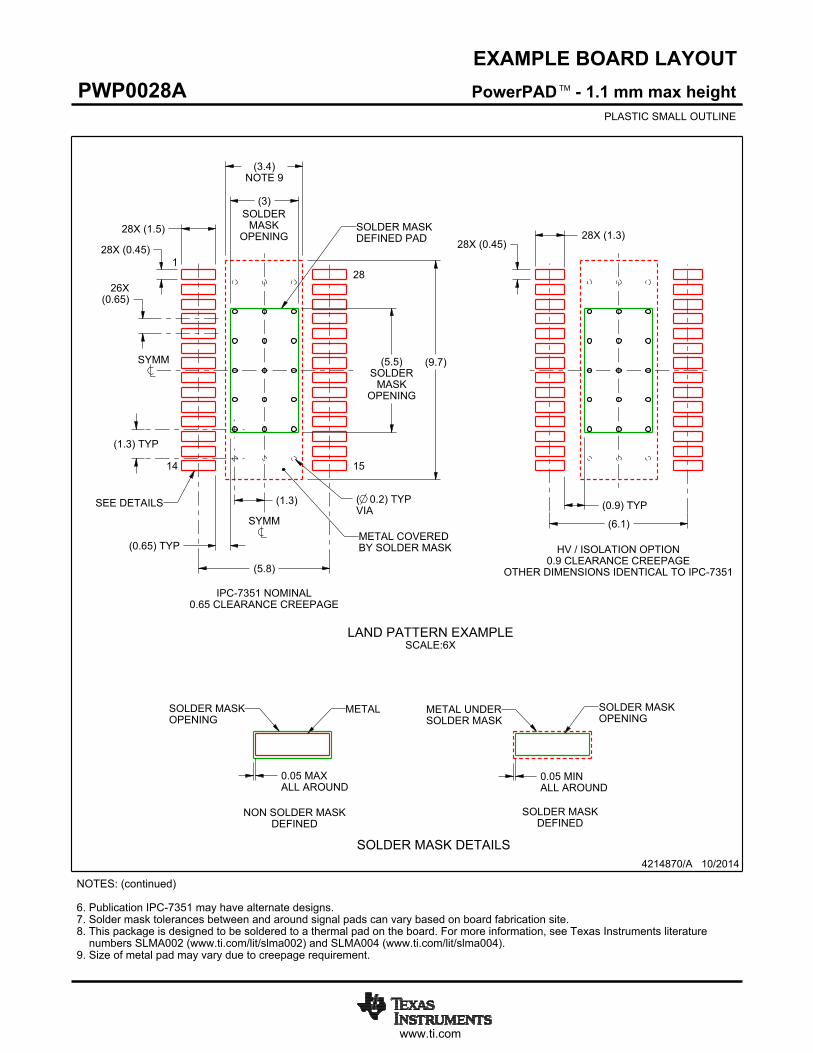
www.ti.com
EXAMPLE BOARD LAYOUT
0.05 MAXALL AROUND
0.05 MINALL AROUND
28X (1.3)
(6.1)
28X (0.45)
(0.9) TYP
28X (1.5)
28X (0.45)
26X(0.65)
(3)
(3.4)NOTE 9
(5.5)SOLDER
MASKOPENING
(9.7)
(1.3)
(1.3) TYP
(5.8)
( ) TYPVIA
0.2
(0.65) TYP
4214870/A 10/2014
PowerPAD - 1.1 mm max heightPWP0028APLASTIC SMALL OUTLINE
SOLDER MASKDEFINED PAD
LAND PATTERN EXAMPLESCALE:6X
HV / ISOLATION OPTION0.9 CLEARANCE CREEPAGE
OTHER DIMENSIONS IDENTICAL TO IPC-7351
TM
NOTES: (continued) 6. Publication IPC-7351 may have alternate designs. 7. Solder mask tolerances between and around signal pads can vary based on board fabrication site. 8. This package is designed to be soldered to a thermal pad on the board. For more information, see Texas Instruments literature numbers SLMA002 (www.ti.com/lit/slma002) and SLMA004 (www.ti.com/lit/slma004).9. Size of metal pad may vary due to creepage requirement.
METALSOLDER MASKOPENING
NON SOLDER MASKDEFINED
SOLDER MASK DETAILS
SOLDER MASKOPENING
METAL UNDERSOLDER MASK
SOLDER MASKDEFINED
SYMM
SYMM
SEE DETAILS
1
14 15
28
METAL COVEREDBY SOLDER MASK
SOLDERMASK
OPENING
IPC-7351 NOMINAL0.65 CLEARANCE CREEPAGE

www.ti.com
EXAMPLE STENCIL DESIGN
28X (1.3)
28X (0.45)
(6.1)
28X (1.5)
28X (0.45)
26X (0.65)
(3)
(5.5)BASED ON
0.127 THICKSTENCIL
(5.8)
4214870/A 10/2014
PowerPAD - 1.1 mm max heightPWP0028APLASTIC SMALL OUTLINE
2.66 X 4.770.1782.88 X 5.160.152
3.0 X 5.5 (SHOWN)0.1273.55 X 6.370.1
SOLDER STENCILOPENING
STENCILTHICKNESS
SEE TABLE FORDIFFERENT OPENINGSFOR OTHER STENCILTHICKNESSES
NOTES: (continued) 10. Laser cutting apertures with trapezoidal walls and rounded corners may offer better paste release. IPC-7525 may have alternate design recommendations. 11. Board assembly site may have different recommendations for stencil design.
TM
SOLDER PASTE EXAMPLEEXPOSED PAD
100% PRINTED SOLDER COVERAGE AREASCALE:6X
HV / ISOLATION OPTION0.9 CLEARANCE CREEPAGE
OTHER DIMENSIONS IDENTICAL TO IPC-7351
SYMM
SYMM
1
14 15
28
BASED ON0.127 THICK
STENCIL BY SOLDER MASKMETAL COVERED
IPC-7351 NOMINAL0.65 CLEARANCE CREEPAGE


IMPORTANT NOTICE
Texas Instruments Incorporated and its subsidiaries (TI) reserve the right to make corrections, enhancements, improvements and otherchanges to its semiconductor products and services per JESD46, latest issue, and to discontinue any product or service per JESD48, latestissue. Buyers should obtain the latest relevant information before placing orders and should verify that such information is current andcomplete. All semiconductor products (also referred to herein as “components”) are sold subject to TI’s terms and conditions of salesupplied at the time of order acknowledgment.TI warrants performance of its components to the specifications applicable at the time of sale, in accordance with the warranty in TI’s termsand conditions of sale of semiconductor products. Testing and other quality control techniques are used to the extent TI deems necessaryto support this warranty. Except where mandated by applicable law, testing of all parameters of each component is not necessarilyperformed.TI assumes no liability for applications assistance or the design of Buyers’ products. Buyers are responsible for their products andapplications using TI components. To minimize the risks associated with Buyers’ products and applications, Buyers should provideadequate design and operating safeguards.TI does not warrant or represent that any license, either express or implied, is granted under any patent right, copyright, mask work right, orother intellectual property right relating to any combination, machine, or process in which TI components or services are used. Informationpublished by TI regarding third-party products or services does not constitute a license to use such products or services or a warranty orendorsement thereof. Use of such information may require a license from a third party under the patents or other intellectual property of thethird party, or a license from TI under the patents or other intellectual property of TI.Reproduction of significant portions of TI information in TI data books or data sheets is permissible only if reproduction is without alterationand is accompanied by all associated warranties, conditions, limitations, and notices. TI is not responsible or liable for such altereddocumentation. Information of third parties may be subject to additional restrictions.Resale of TI components or services with statements different from or beyond the parameters stated by TI for that component or servicevoids all express and any implied warranties for the associated TI component or service and is an unfair and deceptive business practice.TI is not responsible or liable for any such statements.Buyer acknowledges and agrees that it is solely responsible for compliance with all legal, regulatory and safety-related requirementsconcerning its products, and any use of TI components in its applications, notwithstanding any applications-related information or supportthat may be provided by TI. Buyer represents and agrees that it has all the necessary expertise to create and implement safeguards whichanticipate dangerous consequences of failures, monitor failures and their consequences, lessen the likelihood of failures that might causeharm and take appropriate remedial actions. Buyer will fully indemnify TI and its representatives against any damages arising out of the useof any TI components in safety-critical applications.In some cases, TI components may be promoted specifically to facilitate safety-related applications. With such components, TI’s goal is tohelp enable customers to design and create their own end-product solutions that meet applicable functional safety standards andrequirements. Nonetheless, such components are subject to these terms.No TI components are authorized for use in FDA Class III (or similar life-critical medical equipment) unless authorized officers of the partieshave executed a special agreement specifically governing such use.Only those TI components which TI has specifically designated as military grade or “enhanced plastic” are designed and intended for use inmilitary/aerospace applications or environments. Buyer acknowledges and agrees that any military or aerospace use of TI componentswhich have not been so designated is solely at the Buyer's risk, and that Buyer is solely responsible for compliance with all legal andregulatory requirements in connection with such use.TI has specifically designated certain components as meeting ISO/TS16949 requirements, mainly for automotive use. In any case of use ofnon-designated products, TI will not be responsible for any failure to meet ISO/TS16949.
Products ApplicationsAudio www.ti.com/audio Automotive and Transportation www.ti.com/automotiveAmplifiers amplifier.ti.com Communications and Telecom www.ti.com/communicationsData Converters dataconverter.ti.com Computers and Peripherals www.ti.com/computersDLP® Products www.dlp.com Consumer Electronics www.ti.com/consumer-appsDSP dsp.ti.com Energy and Lighting www.ti.com/energyClocks and Timers www.ti.com/clocks Industrial www.ti.com/industrialInterface interface.ti.com Medical www.ti.com/medicalLogic logic.ti.com Security www.ti.com/securityPower Mgmt power.ti.com Space, Avionics and Defense www.ti.com/space-avionics-defenseMicrocontrollers microcontroller.ti.com Video and Imaging www.ti.com/videoRFID www.ti-rfid.comOMAP Applications Processors www.ti.com/omap TI E2E Community e2e.ti.comWireless Connectivity www.ti.com/wirelessconnectivity
Mailing Address: Texas Instruments, Post Office Box 655303, Dallas, Texas 75265Copyright © 2015, Texas Instruments Incorporated