lm6211 low noise, rro operational amplifier with … · lm6211 snosah2c – february 2006–...
TRANSCRIPT

1 10 1k 10k 100k
FREQUENCY (Hz)
1
10
100
1000
100
VO
LTA
GE
NO
ISE
(nV
/H
z)
VS = 5V, 24V
+- VCO
INPUT
CHARGEPUMP
OUTPUT
VS_PLL
2
LM6211
www.ti.com SNOSAH2C –FEBRUARY 2006–REVISED MARCH 2013
LM6211 Low Noise, RRO Operational Amplifier with CMOS Input and 24V OperationCheck for Samples: LM6211
1FEATURES • Temperature Range -40°C to 125°C2(Typical 24V Supply Unless Otherwise Noted) • Total Harmonic Distortion 0.01% @ 1 kHz,
600Ω• Supply Voltage Range 5V to 24V• Output Short Circuit Current 25 mA• Input Referred Voltage Noise 5.5 nV/√HzAPPLICATIONS
• Unity Gain Bandwidth 20 MHz• PLL Loop Filters• 1/f Corner Frequency 400 Hz• Low Noise Active Filters• Slew Rate 5.6 V/μs• Strain Gauge Amplifiers• Supply Current 1.05 mA• Low Noise Microphone Amplifiers• Low Input Capacitance 5.5 pF
DESCRIPTIONThe LM6211 is a wide bandwidth, low noise op amp with a wide supply voltage range and a low input biascurrent. The LM6211 operates with a single supply voltage of 5V to 24V, is unity gain stable, has a ground-sensing CMOS input stage, and offers rail-to-rail output swing.
The LM6211 is designed to provide optimal performance in high voltage, low noise systems. The LM6211 has aunity gain bandwidth of 20 MHz and an input referred voltage noise density of 5.5 nV/√Hz at 10 kHz. TheLM6211 achieves these specifications with a low supply current of only 1 mA. The LM6211 has a low input biascurrent of 2.3 pA, an output short circuit current of 25 mA and a slew rate of 5.6 V/us. The LM6211 also featuresa low common-mode input capacitance of 5.5 pF which makes it ideal for use in wide bandwidth and high gaincircuits. The LM6211 is well suited for low noise applications that require an op amp with very low input biascurrents and a large output voltage swing, like active loop-filters for wide-band PLLs. A low total harmonicdistortion, 0.01% at 1 kHz with loads as high as 600Ω, also makes the LM6211 ideal for high fidelity audio andmicrophone amplifiers.
The LM6211 is available in the small SOT-23 package, allowing the user to implement ultra-small and costeffective board layouts.
Typical Application
These devices have limited built-in ESD protection. The leads should be shorted together or the device placed in conductive foamduring storage or handling to prevent electrostatic damage to the MOS gates.
1
Please be aware that an important notice concerning availability, standard warranty, and use in critical applications ofTexas Instruments semiconductor products and disclaimers thereto appears at the end of this data sheet.
2All trademarks are the property of their respective owners.
PRODUCTION DATA information is current as of publication date. Copyright © 2006–2013, Texas Instruments IncorporatedProducts conform to specifications per the terms of the TexasInstruments standard warranty. Production processing does notnecessarily include testing of all parameters.

LM6211
SNOSAH2C –FEBRUARY 2006–REVISED MARCH 2013 www.ti.com
Absolute Maximum Ratings (1) (2)
ESD Tolerance (3) Human Body Model 2000V
Machine Model 200V
VIN Differential ±0.3V
Supply Voltage (VS = V+ – V−) 25V
Voltage at Input/Output pins V+ +0.3V, V− −0.3V
Storage Temperature Range −65°C to +150°C
Junction Temperature (4) +150°C
Soldering Information Infrared or Convection (20 sec) 235°C
Wave Soldering Lead Temp. (10 sec) 260°C
(1) Absolute Maximum Ratings indicate limits beyond which damage to the device may occur. Operating Ratings indicate conditions forwhich the device is intended to be functional, but specific performance is not ensured. For ensured specifications and the testconditions, see the Electrical Characteristics Tables.
(2) If Military/Aerospace specified devices are required, please contact the TI Sales Office/ Distributors for availability and specifications.(3) Human Body Model is 1.5 kΩ in series with 100 pF. Machine Model is 0Ω in series with 200 pF.(4) The maximum power dissipation is a function of TJ(MAX), θJA, and TA. The maximum allowable power dissipation at any ambient
temperature is PD = (TJ(MAX) - TA)/θJA . All numbers apply for packages soldered directly onto a PC board.
Operating Ratings (1)
Temperature Range −40°C to +125°C
Supply Voltage (VS = V+ – V−) 5V to 24V
Package Thermal Resistance (θJA(2)) 5-Pin SOT-23 178°C/W
(1) Absolute Maximum Ratings indicate limits beyond which damage to the device may occur. Operating Ratings indicate conditions forwhich the device is intended to be functional, but specific performance is not ensured. For ensured specifications and the testconditions, see the Electrical Characteristics Tables.
(2) The maximum power dissipation is a function of TJ(MAX), θJA, and TA. The maximum allowable power dissipation at any ambienttemperature is PD = (TJ(MAX) - TA)/θJA . All numbers apply for packages soldered directly onto a PC board.
5V Electrical Characteristics (1)
Unless otherwise specified, all limits are ensured for TA = 25°C, V+ = 5V, V− = 0V, VCM = VO = V+/2. Boldface limits apply atthe temperature extremes.
Symbol Parameter Conditions Min (2) Typ (3) Max (2) Units
VOS Input Offset Voltage VCM = 0.5V 0.1 ±2.5 mV±2.8
TC VOS Input Offset Average Drift VCM = 0.5V (4) 2 μV/C
IB Input Bias Current VCM = 0.5V (5) (6) 0.5 5 pA10 nA
IOS Input Offset Current VCM = 0.5V 0.1 pA
CMRR Common Mode Rejection Ratio 0 V ≤ VCM ≤ 3V 83 98 dB0.4 V ≤ VCM ≤ 2.3 V 70
PSRR Power Supply Rejection Ratio V+ = 5V to 24V, VCM = 0.5V 85 98 dB78
V+ = 4.5V to 25V, VCM = 0.5V 80 95
CMVR Input Common-Mode Voltage CMRR ≥ 65 dB 0 3.3 VRange CMRR ≥ 60 dB 0 2.4
(1) Electrical table values apply only for factory testing conditions at the temperature indicated. Factory testing conditions result in verylimited self-heating of the device.
(2) Limits are 100% production tested at 25°C. Limits over the operating temperature range are ensured through correlations using theStatistical Quality Control (SQC) method.
(3) Typical values represent the most likely parametric norm at the time of characterization.(4) Offset voltage average drift is determined by dividing the change in VOS at the temperature extremes into the total temperature change.(5) Positive current corresponds to current flowing into the device.(6) Input bias current is ensured by design.
2 Submit Documentation Feedback Copyright © 2006–2013, Texas Instruments Incorporated
Product Folder Links: LM6211

LM6211
www.ti.com SNOSAH2C –FEBRUARY 2006–REVISED MARCH 2013
5V Electrical Characteristics(1) (continued)Unless otherwise specified, all limits are ensured for TA = 25°C, V+ = 5V, V− = 0V, VCM = VO = V+/2. Boldface limits apply atthe temperature extremes.
Symbol Parameter Conditions Min (2) Typ (3) Max (2) Units
AVOL Large Signal Voltage Gain VO = 0.35V to 4.65, RL = 2 kΩ to V+/2 82 11080
dBVO = 0.25V to 4.75, RL = 10 kΩ to V+/2 85 110
82
VO Output Swing High RL = 2 kΩ to V+/2 50 150165
RL = 10 kΩ to V+/2 20 8590 mV from
railOutput Swing Low RL = 2 kΩ to V+/2 39 150170
RL = 10 kΩ to V+/2 13 8590
IOUT Output Short Circuit Current Sourcing to V+/2 13 16VID = 100 mV (7) 10
mASinking to V+/2 20 30VID = −100 mV (7) 10
IS Supply Current 0.96 1.10 mA1.25
SR Slew Rate AV = +1, 10% to 90% (8) 5.5 V/μs
GBW Gain Bandwidth Product 17 MHz
en Input-Referred Voltage Noise f = 10 kHz 5.5nV/√Hz
f = 1 kHz 6.0
in Input-Referred Current Noise f = 1 kHz 0.01 pA/√Hz
THD Total Harmonic Distortion AV = 2, RL = 600Ω to V+/2 0.01 %
(7) The device is short circuit protected and can source or sink its limit currents continuously. However, care should be taken such thatwhen the output is driving short circuit currents, the inputs do not see more than ±0.3V differential voltage.
(8) Slew rate is the average of the rising and falling slew rates.
24V Electrical Characteristics (1)
Unless otherwise specified, all limits are ensured for TA = 25°C, V+ = 24V, V− = 0V, VCM = VO = V+/2. Boldface limits apply atthe temperature extremes.
Symbol Parameter Conditions Min (2) Typ (3) Max (2) Units
VOS Input Offset Voltage VCM = 0.5V 0.25 ±2.7 mV±3.0
TC VOS Input Offset Average Drift VCM = 0.5V (4) ±2 μV/C
IB Input Bias Current VCM = 0.5V (5) (6) 2 25 pA10 nA
IOS Input Offset Current VCM = 0.5V 0.1 pA
CMRR Common Mode Rejection Ratio 0 ≤ VCM ≤ 21V 85 105 dB0.4 ≤ VCM ≤ 20V 70
PSRR Power Supply Rejection Ratio V+ = 5V to 24V, VCM = 0.5V 85 9878 dB
V+ = 4.5V to 25V, VCM = 0.5V 80 98
CMVR Input Common-Mode Voltage CMRR ≥ 65 dB 0 21.5 VRange CMRR ≥ 60 dB 0 20.5
(1) Electrical table values apply only for factory testing conditions at the temperature indicated. Factory testing conditions result in verylimited self-heating of the device.
(2) Limits are 100% production tested at 25°C. Limits over the operating temperature range are ensured through correlations using theStatistical Quality Control (SQC) method.
(3) Typical values represent the most likely parametric norm at the time of characterization.(4) Offset voltage average drift is determined by dividing the change in VOS at the temperature extremes into the total temperature change.(5) Positive current corresponds to current flowing into the device.(6) Input bias current is ensured by design.
Copyright © 2006–2013, Texas Instruments Incorporated Submit Documentation Feedback 3
Product Folder Links: LM6211

VOUT
V-
IN+
V+
IN-
+ -
1
2
3
5
4
LM6211
SNOSAH2C –FEBRUARY 2006–REVISED MARCH 2013 www.ti.com
24V Electrical Characteristics(1) (continued)Unless otherwise specified, all limits are ensured for TA = 25°C, V+ = 24V, V− = 0V, VCM = VO = V+/2. Boldface limits apply atthe temperature extremes.
Symbol Parameter Conditions Min (2) Typ (3) Max (2) Units
AVOL Large Signal Voltage Gain VO = 1.5V to 22.5V, RL = 2 kΩ to V+/2 82 12077
dBVO = 1V to 23V, RL = 10 kΩ to V+/2 85 120
82
VO Output Swing High RL = 2 kΩ to V+/2 212 400520
RL = 10 kΩ to V+/2 48 150165 mV from
railOutput Swing Low RL = 2 kΩ to V+/2 150 350420
RL = 10 kΩ to V+/2 38 150170
IOUT Output Short Circuit Current Sourcing to V+/2 20 25VID = 100 mV (7) 15
mASinking to V+/2 30 38VID = −100 mV (7) 20
IS Supply Current 1.05 1.25 mA1.40
SR Slew Rate AV = +1, VO = 18 VPP 5.6 V/μs10% to 90% (8)
GBW Gain Bandwidth Product 20 MHz
en Input-Referred Voltage Noise f = 10 kHz 5.5nV/√Hz
f = 1 kHz 6.0
in Input-Referred Current Noise f = 1 kHz 0.01 pA/√Hz
THD Total Harmonic Distortion AV = 2, RL = 2 kΩ to V+/2 0.01 %
(7) The device is short circuit protected and can source or sink its limit currents continuously. However, care should be taken such thatwhen the output is driving short circuit currents, the inputs do not see more than ±0.3V differential voltage.
(8) Slew rate is the average of the rising and falling slew rates.
Connection Diagram
Figure 1. 5-Pin SOT-23 - Top View
4 Submit Documentation Feedback Copyright © 2006–2013, Texas Instruments Incorporated
Product Folder Links: LM6211

0 0.5 1 1.5 2 2.5 3 3.5 4
VCM (V)
-2
-1.5
-1
-0.5
0
0.5
1
I BIA
S (
pA)
-40°C
25°C
VS = 5V
0 0.5 1 1.5 2 2.5 3 3.5 4-2.5
2.5
I BIA
S (
nA)
VCM (V)
-2
-1.5
-1
-0.5
0
0.5
1
1.5
2VS = 5V
125°C
0 0.5 1 1.5 2 2.5 3 3.5-1
-0.6
-0.2
0
0.4
0.6
1
VO
S (
mV
)
VCM (V)
0.8
0.2
-0.4
-0.8
125°C
-40°C
25°C
VS = 5V
0 2 4 6 16 18 20 22
VCM (V)
-0.6
-0.4
-0.2
0
0.2
0.4
0.6
0.8
1
VO
S (
mV
)
8 10 12 14
VS = 24V
-40°C
25°C
125°C
5 7 9 11 13 15 17 19 21 230.5
0.6
0.8
1
1.1
1.2
1.4
SU
PP
LY C
UR
RE
NT
(m
A)
VS (V)
1.3
0.9
0.7
125°C
25°C
-40°C
25 5 7 9 11 13 15 17 19 21 23-0.6
-0.4
-0.2
0.2
0.4
0.8
VO
S (
mV
)
VS (V)
0.6
0
125°C
25°C
-40°C
25
LM6211
www.ti.com SNOSAH2C –FEBRUARY 2006–REVISED MARCH 2013
Typical Performance CharacteristicsUnless otherwise specified, TA = 25°C, VS = 24V, V+ = VS, V− = 0 V, VCM = VS/2.
Supply Current VOSvs. vs.
Supply Voltage Supply Voltage
Figure 2. Figure 3.
VOS VOSvs. vs.VCM VCM
Figure 4. Figure 5.
Input Bias Current Input Bias Currentvs. vs.VCM VCM
Figure 6. Figure 7.
Copyright © 2006–2013, Texas Instruments Incorporated Submit Documentation Feedback 5
Product Folder Links: LM6211

4 6 8 10 12 14 16 18 20 22 240
10
20
30
40
50
60
70
VO
UT F
RO
M R
AIL
(m
V)
VS (V)
RL = 10 k:
125°C
-40°C
25°C
4 6 8 10 12 14 16 18 20 22 240
10
20
30
40
50
60
VO
UT F
RO
M R
AIL
(m
V)
VS (V)
RL = 10 k:
125°C
-40°C
25°C
4 6 8 10 12 14 16 18 20 22 24
VS (V)
0
5
10
15
20
25
30
I SO
UR
CE
(m
A)
125°C
-40°C
25°C
I SIN
K (
mA
)
VS (V)
4 6 8 10 12 14 16 18 20 22 240
5
10
15
20
25
30
35
40
45
50
-40°C
25°C
125°C
25°C
0 2 4 6 8 10 12 14 16 18 20-8
-6
-4
-2
0
2
4
I BIA
S (
pA)
VCM (V)
22
-40°C
VS = 24V
0 2 4 6 8 10 12 14 16 18 20-6
-4
-2
0
2
I BIA
S (
nA)
VCM (V)
22
125°C
VS = 24V
LM6211
SNOSAH2C –FEBRUARY 2006–REVISED MARCH 2013 www.ti.com
Typical Performance Characteristics (continued)Unless otherwise specified, TA = 25°C, VS = 24V, V+ = VS, V− = 0 V, VCM = VS/2.
Input Bias Current Input Bias Currentvs. vs.VCM VCM
Figure 8. Figure 9.
Sourcing Current Sinking Currentvs. vs.
Supply Voltage Supply Voltage
Figure 10. Figure 11.
Positive Output Swing Negative Output Swingvs. vs.
Supply Voltage Supply Voltage
Figure 12. Figure 13.
6 Submit Documentation Feedback Copyright © 2006–2013, Texas Instruments Incorporated
Product Folder Links: LM6211

25°C
0 4 8 12 16 20 24
VOUT (V)
0
5
10
15
20
25
30
I SO
UR
CE
(m
A)
125°C
-40°CVS = 24V
-40°C
0 4 8 12 16 20 240
5
10
15
20
25
30
35
40
45
50
I SIN
K (
mA
)
VOUT (V)
VS = 24V
25°C
125°C
125°C
0 1 2 3 4 50
5
10
15
20
25
30
35
40
I SIN
K (
mA
)
VOUT (V)
VS = 5V
-40°C
25°C125°C
0 1 2 3 4 50
2
4
6
8
10
12
14
16
18
20
I SO
UR
CE
(m
A)
VOUT (V)
VS = 5V
-40°C
25°C
4 6 8 10 12 14 16 18 20 22 240
50
100
150
200
250
300
350
VO
UT F
RO
M R
AIL
(m
V)
VS (V)
RL = 2 k:
125°C
-40°C
25°C
4 6 8 10 12 14 16 18 20 22 240
50
100
150
200
250
VO
UT F
RO
M R
AIL
(m
V)
VS (V)
-40°C
RL = 2 k:
125°C25°C
LM6211
www.ti.com SNOSAH2C –FEBRUARY 2006–REVISED MARCH 2013
Typical Performance Characteristics (continued)Unless otherwise specified, TA = 25°C, VS = 24V, V+ = VS, V− = 0 V, VCM = VS/2.
Positive Output Swing Negative Output Swingvs. vs.
Supply Voltage Supply Voltage
Figure 14. Figure 15.
Sourcing Current Sinking Currentvs. vs.
Output Voltage Output Voltage
Figure 16. Figure 17.
Sourcing Current Sinking Currentvs. vs.
Output Voltage Output Voltage
Figure 18. Figure 19.
Copyright © 2006–2013, Texas Instruments Incorporated Submit Documentation Feedback 7
Product Folder Links: LM6211

0.001 0.01 0.1 1 10
OUTPUT AMPLITUDE (V)
0.0001
0.001
0.01
0.1
1
TH
D+
N (
%)
RL = 600:
RL = 100 k:
VS = 5V
0.001 0.1 100
OUTPUT AMPLITUDE (V)
0.0001
0.01
1
TH
D+
N (
%)
1010.01
0.1
0.001
RL = 100 k:
RL = 600:
Vs = 24V
1 10 1k 10k 100k
FREQUENCY (Hz)
1
10
100
1000
100
VO
LTA
GE
NO
ISE
(nV
/H
z)
VS = 5V, 24V
10 100 1k 10k 100k
FREQUENCY (Hz)
0.0001
0.001
0.01
0.1
TH
D+
N (
%) RL = 600:, VS = 5V
RL = 600:, VS = 24V
RL = 100 k:, VS = 24V
RL = 100 k:, VS = 5V
100 10k 1M 100M
FREQUENCY (Hz)
-40
40
100
180
GA
IN (
dB)
10M100k1k
160
80
0
140
120
60
20
-20
-40
40
100
180
160
80
0
140
120
60
20
-20
PH
AS
E (
°)
GAIN
PHASE
RL = 2k:, 10 k:, 10M:
RL = 2k:, 10 k:, 10M:
100 10k 1M 100M
FREQUENCY (Hz)
-40
40
100
180
GA
IN (
dB)
10M100k1k
160
80
0
140
120
60
20
-20
-40
40
100
180
160
80
0
140
120
60
20
-20
PH
AS
E (
°)
GAIN
PHASE
CL = 20 pF
CL = 50 pF
CL = 100 pF
CL = 20 pF, 50 pF, 100 pF
LM6211
SNOSAH2C –FEBRUARY 2006–REVISED MARCH 2013 www.ti.com
Typical Performance Characteristics (continued)Unless otherwise specified, TA = 25°C, VS = 24V, V+ = VS, V− = 0 V, VCM = VS/2.
Open Loop Gain and Phase with Resistive Load Open Loop Gain and Phase with Capacitive Load
Figure 20. Figure 21.
Input Referred Voltage Noise THD+Nvs. vs.
Frequency Frequency
Figure 22. Figure 23.
THD+N THD+Nvs. vs.
Output Amplitude Output Amplitude
Figure 24. Figure 25.
8 Submit Documentation Feedback Copyright © 2006–2013, Texas Instruments Incorporated
Product Folder Links: LM6211

CAPACITIVE LOAD (pF)
10 100 10000
10
20
30
40
50
PH
AS
E M
AR
GIN
(°)
60VS = 5V
RL = 2 k:
RL = 10 k:
RL = 10 M:
CAPACITIVE LOAD (pF)
10 100 10000
10
20
30
40
50
PH
AS
E M
AR
GIN
(°)
60VS = 24V
RL = 2 k:
RL = 10 k:
RL = 10 M:
0 1 2 3 4 5 6 7 8 9 10-0.015
-0.01
-0.005
0
0.005
0.01
0.015
VO
UT (
V)
TIME (Ps)
VS = 24V
CL = 10 pF
0 1 2 3 4 5 6 7 8 9 10-6
-4
-2
0
2
4
6
VO
UT (
V)
TIME (Ps)
VS = 24VCL = 10 pF
5 7 9 11 13 15 17 19 21 23 254.4
4.6
4.8
5
5.2
5.4
5.6
5.8
6
SLE
W R
AT
E (
V/P
s)
VS (V)
FALLING EDGE
RISING EDGE
15 25 35 45 5530
40
50
60
70
OV
ER
SH
OO
T A
ND
UN
DE
RS
HO
OT
(%
)
CAPACITIVE LOAD (pF)
OVERSHOOT %
UNDERSHOOT %
LM6211
www.ti.com SNOSAH2C –FEBRUARY 2006–REVISED MARCH 2013
Typical Performance Characteristics (continued)Unless otherwise specified, TA = 25°C, VS = 24V, V+ = VS, V− = 0 V, VCM = VS/2.
Slew Rate Overshoot and Undershootvs. vs.
Supply Voltage Capacitive Load
Figure 26. Figure 27.
Small Signal Transient Response Large Signal Transient Response
Figure 28. Figure 29.
Phase Margin Phase Marginvs. vs.
Capacitive Load (Stability) Capacitive Load (Stability)
Figure 30. Figure 31.
Copyright © 2006–2013, Texas Instruments Incorporated Submit Documentation Feedback 9
Product Folder Links: LM6211

10 1k 1M
FREQUENCY (Hz)
-120
-80
0
CM
RR
(dB
)
100k10k100
-20
-60
-100
-40
VS = 5V
VS = 24V
10 1k 100k 10M
FREQUENCY (Hz)
0.001
0.1
10
100
ZO
UT (:
)
1M10k100
1
0.01
VS = 5V
VS = 24V
0
10 1k 100k 10M
FREQUENCY (Hz)
-120
-40
PS
RR
(dB
)
1M10k100
-20
-60
-80
-100
VS = 5V, -PSRR
VS = 5V, +PSRR
VS = 24V, -PSRR
VS = 24V, +PSRR
LM6211
SNOSAH2C –FEBRUARY 2006–REVISED MARCH 2013 www.ti.com
Typical Performance Characteristics (continued)Unless otherwise specified, TA = 25°C, VS = 24V, V+ = VS, V− = 0 V, VCM = VS/2.
Closed Loop Output Impedance PSRRvs. vs.
Frequency Frequency
Figure 32. Figure 33.
CMRRvs.
Frequency
Figure 34.
10 Submit Documentation Feedback Copyright © 2006–2013, Texas Instruments Incorporated
Product Folder Links: LM6211
LM6211
www.ti.com SNOSAH2C –FEBRUARY 2006–REVISED MARCH 2013
APPLICATION NOTES
ADVANTAGES OF THE LM6211
High Supply Voltage, Low Power Operation
The LM6211 has performance ensured at supply voltages of 5V and 24V. The LM6211 is ensured to beoperational at all supply voltages between 5V and 24V. In this large range of operation, the LM6211 draws afairly constant supply current of 1 mA, while providing a wide bandwidth of 20 MHz. The wide operating rangemakes the LM6211 a versatile choice for a variety of applications ranging from portable instrumentation toindustrial control systems.
Low Input Referred Noise
The LM6211 has very low flatband input referred voltage noise, 5.5 nV/√Hz. The 1/f corner frequency, also verylow, is about 400 Hz. The CMOS input stage allows for an extremely low input current (2 pA) and a very lowinput referred current noise (0.01 pA/√Hz). This allows the LM6211 to maintain signal fidelity and makes it idealfor audio, wireless or sensor based applications.
Low Input Bias Current and High Input Impedance
The LM6211 has a CMOS input stage, which allows it to have very high input impedance, very small input biascurrents (2 pA) and extremely low input referred current noise (0.01 pA/√Hz). This level of performance isessential for op amps used in sensor applications, which deal with extremely low currents of the order of a fewnanoamperes. In this case, the op amp is being driven by a sensor, which typically has a source impedance oftens of MΩ. This makes it essential for the op amp to have a much higher impedance.
Low Input Capacitance
The LM6211 has a comparatively small input capacitance for a high voltage CMOS design. Low inputcapacitance is very beneficial in terms of driving large feedback resistors, required for higher closed loop gain.Usually, high voltage CMOS input stages have a large input capacitance, which when used in a typical gainconfiguration, interacts with the feedback resistance to create an extra pole. The extra pole causes gain-peakingand can compromise the stability of the op amp. The LM6211 can, however, be used with larger resistors due toits smaller input capacitance, and hence provide more gain without compromising stability. This also makes theLM6211 ideal for wideband transimpedance amplifiers, which require a wide bandwidth, low input referred noiseand low input capacitance.
RRO, Ground Sensing and Current Limiting
The LM6211 has a rail-to-rail output stage, which provides the maximum possible output dynamic range. This isespecially important for applications requiring a large output swing, like wideband PLL synthesizers which needan active loop filter to drive a wide frequency range VCO. The input common mode range includes the negativesupply rail which allows direct sensing at ground in a single supply operation. The LM6211 also has a shortcircuit protection circuit which limits the output current to about 25 mA sourcing and 38 mA sinking, and allowsthe LM6211 to drive short circuit loads indefinitely. However, while driving short circuit loads care should betaken to prevent the inputs from seeing more than ±0.3V differential voltage, which is the absolute maximumdifferential input voltage.
Small Size
The small footprint of the LM6211 package saves space on printed circuit boards, and enables the design ofsmaller and more compact electronic products. Long traces between the signal source and the op amp make thesignal path susceptible to noise. By using a physically smaller package, the LM6211 can be placed closer to thesignal source, reducing noise pickup and enhancing signal integrity
Copyright © 2006–2013, Texas Instruments Incorporated Submit Documentation Feedback 11
Product Folder Links: LM6211

ROUT
-
+VIN
RF
CF
RIN
RLCL
RS
0
UNSTABLEROC = 40 dB/decade
STABLEROC ± 20 dB/decade
FREQUENCY (Hz)
GA
IN
LM6211
SNOSAH2C –FEBRUARY 2006–REVISED MARCH 2013 www.ti.com
STABILITY OF OP AMP CIRCUITS
Stability and Capacitive Loading
The LM6211 is designed to be unity gain stable for moderate capacitive loads, around 100 pF. That is, ifconnected in a unity gain buffer configuration, the LM6211 will resist oscillation unless the capacitive load ishigher than about 100 pF. For higher capacitive loads, the phase margin of the op amp reduces significantly andit tends to oscillate. This is because an op amp cannot be designed to be stable for high capacitive loads withouteither sacrificing bandwidth or supplying higher current. Hence, for driving higher capacitive loads, the LM6211needs to be externally compensated.
Figure 35. Gain vs. Frequency for an Op Amp
An op amp, ideally, has a dominant pole close to DC, which causes its gain to decay at the rate of 20 dB/decadewith respect to frequency. If this rate of decay, also known as the rate of closure (ROC), remains at 20dB/decade at the unity gain bandwidth of the op amp, the op amp is stable. If, however, a large capacitance isadded to the output of the op amp, it combines with the output impedance of the op amp to create another polein its frequency response before its unity gain frequency (Figure 35). This increases the ROC to 40 dB/decadeand causes instability.
In such a case a number of techniques can be used to restore stability to the circuit. The idea behind all theseschemes is to modify the frequency response such that it can be restored to a ROC of 20 dB/decade, whichensures stability.
In the Loop Compensation
Figure 36 illustrates a compensation technique, known as ‘in the loop’ compensation, that employs an RCfeedback circuit within the feedback loop to stabilize a non-inverting amplifier configuration. A small seriesresistance, RS, is used to isolate the amplifier output from the load capacitance, CL, and a small capacitance, CF,is inserted across the feedback resistor to bypass CL at higher frequencies.
Figure 36. In the Loop Compensation
12 Submit Documentation Feedback Copyright © 2006–2013, Texas Instruments Incorporated
Product Folder Links: LM6211

CF = ¨¨
©
§RF + 2RIN
RF2
¨¨
©
§CLROUT
RS = ROUTRIN
RF
LM6211
www.ti.com SNOSAH2C –FEBRUARY 2006–REVISED MARCH 2013
The values for RS and CF are decided by ensuring that the zero attributed to CF lies at the same frequency as thepole attributed to CL. This ensures that the effect of the second pole on the transfer function is compensated forby the presence of the zero, and that the ROC is maintained at 20 dB/decade. For the circuit shown in Figure 36the values of RS and CF are given by Equation 1. Table 1 shows different values of RS and CF that need to beused for maintaining stability with different values of CL, as well as the phase margins to be expected. RF and RINare assumed to be 10 kΩ, RL is taken as 2 kΩ, while ROUT is taken to be 60Ω.
(1)
Table 1.
CL (pF) RS (Ω) CF (pF) Phase Margin (°)
250 60 4.5 39.8
300 60 5.4 49.5
500 60 9 53.1
Although this methodology provides circuit stability for any load capacitance, it does so at the price of bandwidth.The closed loop bandwidth of the circuit is now limited by RS and CF.
Compensation by External Resistor
In some applications it is essential to drive a capacitive load without sacrificing bandwidth. In such a case, in theloop compensation is not viable. A simpler scheme for compensation is shown in Figure 37. A resistor, RISO, isplaced in series between the load capacitance and the output. T110his introduces a zero in the circuit transferfunction, which counteracts the effect of the pole formed by the load capacitance, and ensures stability.
Figure 37. Compensation By Isolation Resistor
The value of RISO to be used should be decided depending on the size of CL and the level of performancedesired. Values ranging from 5Ω to 50Ω are usually sufficient to ensure stability. A larger value of RISO will resultin a system with lesser ringing and overshoot, but will also limit the output swing and the short circuit current ofthe circuit.
Stability and Input Capacitance
In certain applications, for example I-V conversion, transimpedance photodiode amplification and buffering theoutput of current-output DAC, capacitive loading at the input of the op amp can endanger stability. Thecapacitance of the source driving the op amp, the op amp input capacitance and the parasitic/wiring capacitancecontribute to the loading of the input. This capacitance, CIN, interacts with the feedback network to introduce apeaking in the closed loop gain of the circuit, and hence causes instability.
Copyright © 2006–2013, Texas Instruments Incorporated Submit Documentation Feedback 13
Product Folder Links: LM6211

+- VCO
INPUT
CHARGEPUMP
OUTPUT
VS_PLL
2
CIN
R1
R2
VOUT
+
-
+
-
VIN+
-
CF
LM6211
SNOSAH2C –FEBRUARY 2006–REVISED MARCH 2013 www.ti.com
Figure 38. Compensating for Input Capacitance
This peaking can be eliminated by adding a feedback capacitance, CF, as shown in Figure 38. This introduces azero in the feedback network, and hence a pole in the closed loop response, and thus maintains stability. Anoptimal value of CF is given by Equation 2. A simpler approach is to select CF = (R1/R2)CIN for a 90° phasemargin. This approach, however, limits the bandwidth excessively.
Typical Applications
ACTIVE LOOP FILTER FOR PLLs
A typical phase locked loop, or PLL, functions by creating a negative feedback loop in terms of the phase of asignal. A simple PLL consists of three main components: a phase detector, a loop filter and a voltage controlledoscillator (VCO). The phase detector compares the phase of the output of the PLL with that of a reference signal,and feeds the error signal into the loop filter, thus performing negative feedback. The loop filter performs theimportant function of averaging (or low-pass filtering) the error and providing the VCO with a DC voltage, whichallows the VCO to modify its frequency such that the error is minimized. The performance of the loop filter affectsa number of specifications of the PLL, like its frequency range, locking time and phase noise.
Since a loop filter is a very noise sensitive application, it is usually suggested that only passive components beused in its design. Any active devices, like discrete transistors or op amps, would add significantly to the noise ofthe circuit and would hence worsen the in-band phase noise of the PLL. But newer and faster PLLs, like TI’sLMX2430, have a power supply voltage of less than 3V, which limits the phase-detector output of the PLL. If apassive loop filter is used with such circuits, then the DC voltage that can be provided to the VCO is limited tocouple of volts. This limits the range of frequencies for which the VCO, and hence the PLL, is functional. Incertain applications requiring a wider operating range of frequencies for the PLL, like set-top boxes or basestations, this level of performance is not adequate and requires active amplification, hence the need for activeloop filters.
An active loop filter typically consists of an op amp, which provides the gain, accompanied by a three or four poleRC filter. The non-inverting input of the op amp is biased to a fixed value, usually the mid-supply of the PLL,while a feedback network provides the gain as well as one, or two, poles for low pass filtering. Figure 39illustrates a typical active loop filter.
Figure 39. A Typical Active Loop Filter
14 Submit Documentation Feedback Copyright © 2006–2013, Texas Instruments Incorporated
Product Folder Links: LM6211

1k 10k 100k 1M
OFFSET FREQUENCY (Hz)
-1.0
0.0
1.0
2.0
3.0
4.0
AD
DE
D P
HA
SE
NO
ISE
(dB
) ACTIVE LOOP FILTER WITH LM6211
PASSIVE LOOP FILTER
LM6211
www.ti.com SNOSAH2C –FEBRUARY 2006–REVISED MARCH 2013
Certain performance characteristics are essential for an op amp if it is to be used in a PLL loop filter. Low inputreferred voltage and current noise are essential, as they directly affect the noise of the filter and hence the phasenoise of the PLL. Low input bias current is also important, as bias current affects the level of ‘reference spurs’,artifacts in the frequency spectrum of the PLL caused by mismatch or leakage at the output of the phasedetector. A large input and output swing is beneficial in terms of increasing the flexibility in biasing the op amp.The op amp can then be biased such that the output range of the PLL is mapped efficiently onto the input rangeof the VCO.
With a CMOS input, ultra low input bias currents (2 pA) and low input referred voltage noise (5.5 nV/√Hz), theLM6211 is an ideal op amp for using in a PLL active loop filter. The LM6211 has a ground sensing input stage, arail-to-rail output stage, and an operating supply range of 5V - 24V, which makes it a versatile choice for thedesign of a wide variety of active loop filters.
Figure 41 shows the LM6211 used with the LMX2430 to create an RF frequency synthesizer. The LMX2430detects the PLL output, compares it with its internal reference clock and outputs the phase error in terms ofcurrent spikes. The LM6211 is used to create a loop filter which averages the error and provides a DC voltage tothe VCO. The VCO generates a sine wave at a frequency determined by the DC voltage at its input. This circuitcan provide output signal frequencies as high as 2 GHz, much higher than a comparative passive loop filter.Compared to a similar passive loop filter, the LM6211 doesn’t add significantly to the phase noise of the PLL,except at the edge of the loop bandwidth, as shown in Figure 40. A peaking of loop gain is expected, since theloop filter is deliberately designed to have a wide bandwidth and a low phase margin so as to minimize lockingtime.
Figure 40. Effect of LM6211 on Phase Noise of PLL
Copyright © 2006–2013, Texas Instruments Incorporated Submit Documentation Feedback 15
Product Folder Links: LM6211

VS
DA
TA
CLK
VS
F0L
D
FL 0
_RF
GND LE
FIN_IF VS
CE FINB_RF
D0_IF
OSC_EN
OSC_OUT/FL0_IF
OSC_IN
FIN_RF
GND
D0_RF
GND
17
16
15
14
13
12
11
1
2
3
4
5
6
7
C260.01 PF
C27100 pF
IF_PLL I/O's
RF_PLL PROGRAMMING INPUTS
8 9 10
20 19 18
C130.01 PF
C14100 pF
C100.01 PF
C11100 pF
C5100 pF
C1 C2 C4
R2
-
+
C6100 pF
VS_PLL
R46100 k:
R45100 k:
C370.1 PF
C39
R47 C38
R5010:
C410.1 PF
VS_OP AMP
3 2 1 16
7
6
5
4
12
13
14
15
8 9 10 11
RF
OU
T
VCC
V+
C80.01 PF
VS_RF
L2
C9100 pF
V586ME04
R518:
R718:
C7100 pF RF_OUT
R618:
C40100 pF
VS_PLL
R3 R41
C36C3
VS_PLL
VS_PLL
LM6211
LMX2430
LM6211
SNOSAH2C –FEBRUARY 2006–REVISED MARCH 2013 www.ti.com
Figure 41. LM6211 in the Active Loop Filter for LMX2430
ADC INPUT DRIVER
A typical application for a high performance op amp is as an ADC driver, which delivers the analog signalobtained from sensors and actuators to ADCs for conversion to the digital domain and further processing.Important requirements in this application are a slew rate high enough to drive the ADC input and low inputreferred voltage and current noise. If an op amp is used with an ADC, it is critical that the op amp noise does notaffect the dynamic range of the ADC. The LM6211, with low input referred voltage and current noise, provides agreat solution for this application. For example, the LM6211 can be used to drive an ADS121021, a 12-bit ADCfrom TI. If it provides a gain of 10 to a maximum input signal amplitude of 100 mV, for a bandwidth as wide as100 kHz, the average noise seen at the input of the ADC is only 44.6 µVrms. Hence the dynamic range of theADC, measured in Effective Number of Bits or ENOB, is only reduced by 0.3 bits, despite amplifying the inputsignal by a gain of 10. Low input bias currents and high input impedance also help as they prevent the loading ofthe sensor and allow the measurement system to function over a large range.
Figure 42 shows a circuit for monitoring fluid pressure in a hydraulic system, in which the LM6211 is used tosense the error voltage from the pressure sensor. Two LM6211 amplifiers are used to make a differenceamplifier which senses the error signal, amplifies it by a gain of 100, and delivers it to the ADC input. The ADCconverts the error voltage into a pressure reading to be displayed and drives the DAC, which changes thevoltage driving the resistance bridge sensor. This is used to control the gain of the pressure measurement circuit,such that the range of the sensor can be modified to obtain the best resolution possible.
16 Submit Documentation Feedback Copyright © 2006–2013, Texas Instruments Incorporated
Product Folder Links: LM6211

DAC081S101SCLK 5
DOUT 4
SYNC 6
2
3LM6211
10 PF
0.1 PF
VS
-
+1
VS
+IN
-INC2
B10.1 PF 1 PF
+5V4
56
1,2 7,8
7 SCLK
6 DOUT
5 CS
C1
6 SYNC
5 SCLK
4 DOUT
2
3
4.096V
1VOUT
120 pF
+
-
A2
-
+
A1
3
42
15
+5V
100 k: 0.2 PF
180:
100 k: 0.2 PF470 pF
470 pF 1 8
4
2.048VVREF
+5V
2
3
+5V
5
1
24
3
AV = 100
180:
2.02 k:
PRESSURE SENSOR0.2 mV/Volt/PSI
A1, A2 = LM6211B1 = LM4140ACM-2.0C1 = DAC081S101C2 = ADC121S625
LM6211
www.ti.com SNOSAH2C –FEBRUARY 2006–REVISED MARCH 2013
Figure 42. Hydraulic Pressure Monitoring System
DAC OUTPUT AMPLIFIER
Op amps are often used to improve a DAC's output driving capability. High performance op amps are required asI-V converters at the outputs of high resolution current output DACs. Since most DACs operate with a singlesupply of 5V, a rail-to-rail output swing is essential for this application. A low offset voltage is also necessary toprevent offset errors in the waveform generated. Also, the output impedance of DACs is quite high, more than afew kΩ in some cases, so it is also advisable for the op amp to have a low input bias current. An op amp with ahigh input impedance also prevents the loading of the DAC, and hence, avoids gain errors. The op amp shouldalso have a slew rate which is fast enough to not affect the settling time of the DAC output.
The LM6211, with a CMOS input stage, ultra low input bias current, a wide bandwidth (20 MHz) and a rail-to-railoutput swing for a supply voltage of 24V is an ideal op amp for such an application. Figure 43 shows a typicalcircuit for this application. The op amp is usually expected to add another time constant to the system, whichworsens the settling time, but the wide bandwidth of the LM6211 (20 MHz) allows the system performance toimprove without any significant degradation of the settling time.
Figure 43. DAC Driver Circuit
Copyright © 2006–2013, Texas Instruments Incorporated Submit Documentation Feedback 17
Product Folder Links: LM6211

CC2RB1
RB2
CF
CC1
V+
AV = 1 +R2
R1
+-VIN
+
-
R11 k:
R210 k:
VOUT
+
-
= 11
CC1
+VOUT
+
-
-
CF
VIN+
-
RB1
V+
RB2
CC2
R2
R1AV = - = -10
R210 k:
R11 k:
LM6211
SNOSAH2C –FEBRUARY 2006–REVISED MARCH 2013 www.ti.com
AUDIO PREAMPLIFIER
With low input referred voltage noise, low supply voltage and low supply current, and low harmonic distortion, theLM6211 is ideal for audio applications. Its wide unity gain bandwidth allows it to provide large gain over a widefrequency range and it can be used to design a preamplifier to drive a load of as low as 600Ω with less than0.001% distortion. Two amplifier circuits are shown in Figure 44 and Figure 45. Figure 44 is an invertingamplifier, with a 10 kΩ feedback resistor, R2, and a 1 kΩ input resistor, R1, and hence provides a gain of −10.Figure 45 is a non-inverting amplifier, using the same values for R1 and R2, and provides a gain of 11. In either ofthese circuits, the coupling capacitor CC1 decides the lower frequency at which the circuit starts providing gain,while the feedback capacitor CF decides the frequency at which the gain starts dropping off. Figure 46 shows thefrequency response of the circuit in Figure 44 with different values of CF.
Figure 44. Inverting Audio Amplifier
Figure 45. Non-Inverting Audio Preamplifier
18 Submit Documentation Feedback Copyright © 2006–2013, Texas Instruments Incorporated
Product Folder Links: LM6211

CCM
IIN
RF
VOUT
+
-
+
-
VB
CF
CD
VOUT
IIN- RF =
CIN = CD + CCM
25
1 100 10k 1M
FREQUENCY (Hz)
-20
-5
10
GA
IN (
dB)
100k1k10
20
15
5
0
-10
-15
CF = 10 pF
CF = 100 pF
CF = 1 nF
LM6211
www.ti.com SNOSAH2C –FEBRUARY 2006–REVISED MARCH 2013
Figure 46. Frequency Response of the Non-Inverting Preamplifier
TRANSIMPEDANCE AMPLIFIER
A transimpedance amplifier converts a small input current into a voltage. This current is usually generated by aphotodiode. The transimpedance gain, measured as the ratio of the output voltage to the input current, isexpected to be large and wide-band. Since the circuit deals with currents in the range of a few nA, low noiseperformance is essential. The LM6211, being a CMOS input op amp, provides a wide bandwidth and low noiseperformance while drawing very low input bias current, and is hence ideal for transimpedance applications.
A transimpedance amplifier is designed on the basis of the current source driving the input. A photodiode is avery common capacitive current source, which requires transimpedance gain for transforming its minisculecurrent into easily detectable voltages. The photodiode and amplifier’s gain are selected with respect to thespeed and accuracy required of the circuit. A faster circuit would require a photodiode with lesser capacitanceand a faster amplifier. A more sensitive circuit would require a sensitive photodiode and a high gain. A typicaltransimpedance amplifier is shown in Figure 47. The output voltage of the amplifier is given by the equationVOUT = −IINRF. Since the output swing of the amplifier is limited, RF should be selected such that all possiblevalues of IIN can be detected.
The LM6211 has a large gain-bandwidth product (20 MHz), which enables high gains at wide bandwidths. A rail-to-rail output swing at 24V supply allows detection and amplification of a wide range of input currents. A CMOSinput stage with negligible input current noise and low input voltage noise allows the LM6211 to provide highfidelity amplification for wide bandwidths. These properties make the LM6211 ideal for systems requiring wide-band transimpedance amplification.
Figure 47. Photodiode Transimpedance Amplifier
The following parameters are used to design a transimpedance amplifier: the amplifier gain-bandwidth product,A0; the amplifier input capacitance, CCM; the photodiode capacitance, CD; the transimpedance gain required, RF;and the amplifier output swing. Once a feasible RF is selected using the amplifier output swing, these numberscan be used to design an amplifier with the desired transimpedance gain and a maximally flat frequencyresponse. The input common-mode capacitance with respect to VCM for the LM6211 is give in Figure 48.
Copyright © 2006–2013, Texas Instruments Incorporated Submit Documentation Feedback 19
Product Folder Links: LM6211

+
RF
-
CF
IF RA < < RF
CFc = ¨©
§1 +RB
RA
¨©
§
RA
CFc
RB
RFCINA0CF =
2SRFA0
1 + 1 + 4S
CIN
(pF
)
0 4 8 12 16 18 22 24
VCM (V)
0
5
10
15
20
20141062
VS = 5V
VS = 24V
LM6211
SNOSAH2C –FEBRUARY 2006–REVISED MARCH 2013 www.ti.com
Figure 48. Input Common-Mode Capacitance vs. VCM
An essential component for obtaining a maximally flat response is the feedback capacitor, CF. The capacitanceseen at the input of the amplifier, CIN, combined with the feedback resistor, RF, generates a phase lag whichcauses gain-peaking and can destabilize the circuit. CIN is usually just the sum of CD and CCM. The feedbackcapacitor CF creates a pole, fP in the noise gain of the circuit, which neutralizes the zero in the noise gain, fZ,created by the combination of RF and CIN. If properly positioned, the noise gain pole created by CF can ensurethat the slope of the gain remains at 20 dB/decade till the unity gain frequency of the amplifier is reached, thusensuring stability. As shown in Figure 50, fP is positioned such that it coincides with the point where the noisegain intersects the op amp’s open loop gain. In this case, fP is also the overall 3 dB frequency of thetransimpedance amplifier. The value of CF needed to make it so is given by Equation 2. A larger value of CFcauses excessive reduction of bandwidth, while a smaller value fails to prevent gain peaking and maintainstability.
(2)
Calculating CF from Equation 2 can sometimes return unreasonably small values (<1 pF), especially for highspeed applications. In these cases, it is often more practical to use the circuit shown in Figure 49 in order toallow more reasonable values. In this circuit, the capacitance CF' is (1+ RB/RA) times the effective feedbackcapacitance, CF. A larger capacitor can now be used in this circuit to obtain a smaller effective capacitance.
Figure 49. Modifying CF
For example, if a CF of 0.5 pF is needed, while only a 5 pF capacitor is available, RB and RA can be selectedsuch that RB/RA = 9. This would convert a CF' of 5 pF into a CF of 0.5 pF. This relationship holds as long as RA<< RF
20 Submit Documentation Feedback Copyright © 2006–2013, Texas Instruments Incorporated
Product Folder Links: LM6211
+
VOUT+
-
-
RACF
VIN = KI+
-IR RADIATIONINTENSITY, I
VOUT RA
K(RA + RB)I =
IR SENSOR
RB
OP AMPOPEN LOOPGAIN
NOISE GAIN WITH NO CF
NOISE GAIN WITH CF
fZ fP A0
fZ = 1
2SRFCIN
fP = A0
2SRF(CIN+CF)G
AIN
FREQUENCY
LM6211
www.ti.com SNOSAH2C –FEBRUARY 2006–REVISED MARCH 2013
Figure 50. Method for CF selection
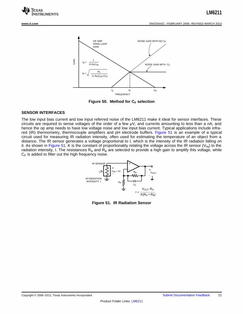
SENSOR INTERFACES
The low input bias current and low input referred noise of the LM6211 make it ideal for sensor interfaces. Thesecircuits are required to sense voltages of the order of a few μV, and currents amounting to less than a nA, andhence the op amp needs to have low voltage noise and low input bias current. Typical applications include infra-red (IR) thermometry, thermocouple amplifiers and pH electrode buffers. Figure 51 is an example of a typicalcircuit used for measuring IR radiation intensity, often used for estimating the temperature of an object from adistance. The IR sensor generates a voltage proportional to I, which is the intensity of the IR radiation falling onit. As shown in Figure 51, K is the constant of proportionality relating the voltage across the IR sensor (VIN) to theradiation intensity, I. The resistances RA and RB are selected to provide a high gain to amplify this voltage, whileCF is added to filter out the high frequency noise.
Figure 51. IR Radiation Sensor
Copyright © 2006–2013, Texas Instruments Incorporated Submit Documentation Feedback 21
Product Folder Links: LM6211

LM6211
SNOSAH2C –FEBRUARY 2006–REVISED MARCH 2013 www.ti.com
REVISION HISTORY
Changes from Revision B (March 2013) to Revision C Page
• Changed layout of National Data Sheet to TI format .......................................................................................................... 21
22 Submit Documentation Feedback Copyright © 2006–2013, Texas Instruments Incorporated
Product Folder Links: LM6211

PACKAGE OPTION ADDENDUM
www.ti.com 27-Jul-2016
Addendum-Page 1
PACKAGING INFORMATION
Orderable Device Status(1)
Package Type PackageDrawing
Pins PackageQty
Eco Plan(2)
Lead/Ball Finish(6)
MSL Peak Temp(3)
Op Temp (°C) Device Marking(4/5)
Samples
LM6211 MDC ACTIVE DIESALE Y 0 400 Green (RoHS& no Sb/Br)
Call TI Level-1-NA-UNLIM -40 to 85
LM6211MF NRND SOT-23 DBV 5 1000 TBD Call TI Call TI -40 to 125 AT1A
LM6211MF/NOPB ACTIVE SOT-23 DBV 5 1000 Green (RoHS& no Sb/Br)
CU SN Level-1-260C-UNLIM -40 to 125 AT1A
LM6211MFX/NOPB ACTIVE SOT-23 DBV 5 3000 Green (RoHS& no Sb/Br)
CU SN Level-1-260C-UNLIM -40 to 125 AT1A
(1) The marketing status values are defined as follows:ACTIVE: Product device recommended for new designs.LIFEBUY: TI has announced that the device will be discontinued, and a lifetime-buy period is in effect.NRND: Not recommended for new designs. Device is in production to support existing customers, but TI does not recommend using this part in a new design.PREVIEW: Device has been announced but is not in production. Samples may or may not be available.OBSOLETE: TI has discontinued the production of the device.
(2) Eco Plan - The planned eco-friendly classification: Pb-Free (RoHS), Pb-Free (RoHS Exempt), or Green (RoHS & no Sb/Br) - please check http://www.ti.com/productcontent for the latest availabilityinformation and additional product content details.TBD: The Pb-Free/Green conversion plan has not been defined.Pb-Free (RoHS): TI's terms "Lead-Free" or "Pb-Free" mean semiconductor products that are compatible with the current RoHS requirements for all 6 substances, including the requirement thatlead not exceed 0.1% by weight in homogeneous materials. Where designed to be soldered at high temperatures, TI Pb-Free products are suitable for use in specified lead-free processes.Pb-Free (RoHS Exempt): This component has a RoHS exemption for either 1) lead-based flip-chip solder bumps used between the die and package, or 2) lead-based die adhesive used betweenthe die and leadframe. The component is otherwise considered Pb-Free (RoHS compatible) as defined above.Green (RoHS & no Sb/Br): TI defines "Green" to mean Pb-Free (RoHS compatible), and free of Bromine (Br) and Antimony (Sb) based flame retardants (Br or Sb do not exceed 0.1% by weightin homogeneous material)
(3) MSL, Peak Temp. - The Moisture Sensitivity Level rating according to the JEDEC industry standard classifications, and peak solder temperature.
(4) There may be additional marking, which relates to the logo, the lot trace code information, or the environmental category on the device.
(5) Multiple Device Markings will be inside parentheses. Only one Device Marking contained in parentheses and separated by a "~" will appear on a device. If a line is indented then it is a continuationof the previous line and the two combined represent the entire Device Marking for that device.
(6) Lead/Ball Finish - Orderable Devices may have multiple material finish options. Finish options are separated by a vertical ruled line. Lead/Ball Finish values may wrap to two lines if the finishvalue exceeds the maximum column width.

PACKAGE OPTION ADDENDUM
www.ti.com 27-Jul-2016
Addendum-Page 2
Important Information and Disclaimer:The information provided on this page represents TI's knowledge and belief as of the date that it is provided. TI bases its knowledge and belief on informationprovided by third parties, and makes no representation or warranty as to the accuracy of such information. Efforts are underway to better integrate information from third parties. TI has taken andcontinues to take reasonable steps to provide representative and accurate information but may not have conducted destructive testing or chemical analysis on incoming materials and chemicals.TI and TI suppliers consider certain information to be proprietary, and thus CAS numbers and other limited information may not be available for release.
In no event shall TI's liability arising out of such information exceed the total purchase price of the TI part(s) at issue in this document sold by TI to Customer on an annual basis.

TAPE AND REEL INFORMATION
*All dimensions are nominal
Device PackageType
PackageDrawing
Pins SPQ ReelDiameter
(mm)
ReelWidth
W1 (mm)
A0(mm)
B0(mm)
K0(mm)
P1(mm)
W(mm)
Pin1Quadrant
LM6211MF SOT-23 DBV 5 1000 178.0 8.4 3.2 3.2 1.4 4.0 8.0 Q3
LM6211MF/NOPB SOT-23 DBV 5 1000 178.0 8.4 3.2 3.2 1.4 4.0 8.0 Q3
LM6211MFX/NOPB SOT-23 DBV 5 3000 178.0 8.4 3.2 3.2 1.4 4.0 8.0 Q3
PACKAGE MATERIALS INFORMATION
www.ti.com 20-Dec-2016
Pack Materials-Page 1

*All dimensions are nominal
Device Package Type Package Drawing Pins SPQ Length (mm) Width (mm) Height (mm)
LM6211MF SOT-23 DBV 5 1000 210.0 185.0 35.0
LM6211MF/NOPB SOT-23 DBV 5 1000 210.0 185.0 35.0
LM6211MFX/NOPB SOT-23 DBV 5 3000 210.0 185.0 35.0
PACKAGE MATERIALS INFORMATION
www.ti.com 20-Dec-2016
Pack Materials-Page 2


www.ti.com
PACKAGE OUTLINE
C
TYP0.220.08
0.25
3.02.6
2X 0.95
1.9
1.45 MAX
TYP0.150.00
5X 0.50.3
TYP0.60.3
TYP80
1.9
A
3.052.75
B1.751.45
(1.1)
SOT-23 - 1.45 mm max heightDBV0005ASMALL OUTLINE TRANSISTOR
4214839/C 04/2017
NOTES: 1. All linear dimensions are in millimeters. Any dimensions in parenthesis are for reference only. Dimensioning and tolerancing per ASME Y14.5M.2. This drawing is subject to change without notice.3. Refernce JEDEC MO-178.
0.2 C A B
1
34
5
2
INDEX AREAPIN 1
GAGE PLANE
SEATING PLANE
0.1 C
SCALE 4.000

www.ti.com
EXAMPLE BOARD LAYOUT
0.07 MAXARROUND
0.07 MINARROUND
5X (1.1)
5X (0.6)
(2.6)
(1.9)
2X (0.95)
(R0.05) TYP
4214839/C 04/2017
SOT-23 - 1.45 mm max heightDBV0005ASMALL OUTLINE TRANSISTOR
NOTES: (continued) 4. Publication IPC-7351 may have alternate designs. 5. Solder mask tolerances between and around signal pads can vary based on board fabrication site.
SYMM
LAND PATTERN EXAMPLEEXPOSED METAL SHOWN
SCALE:15X
PKG
1
3 4
5
2
SOLDER MASKOPENINGMETAL UNDER
SOLDER MASK
SOLDER MASKDEFINED
EXPOSED METAL
METALSOLDER MASKOPENING
NON SOLDER MASKDEFINED
(PREFERRED)
SOLDER MASK DETAILS
EXPOSED METAL

www.ti.com
EXAMPLE STENCIL DESIGN
(2.6)
(1.9)
2X(0.95)
5X (1.1)
5X (0.6)
(R0.05) TYP
SOT-23 - 1.45 mm max heightDBV0005ASMALL OUTLINE TRANSISTOR
4214839/C 04/2017
NOTES: (continued) 6. Laser cutting apertures with trapezoidal walls and rounded corners may offer better paste release. IPC-7525 may have alternate design recommendations. 7. Board assembly site may have different recommendations for stencil design.
SOLDER PASTE EXAMPLEBASED ON 0.125 mm THICK STENCIL
SCALE:15X
SYMM
PKG
1
3 4
5
2

www.ti.com
PACKAGE OUTLINE
C
TYP0.220.08
0.25
3.02.6
2X 0.95
1.9
1.45 MAX
TYP0.150.00
5X 0.50.3
TYP0.60.3
TYP80
1.9
A
3.052.75
B1.751.45
(1.1)
SOT-23 - 1.45 mm max heightDBV0005ASMALL OUTLINE TRANSISTOR
4214839/C 04/2017
NOTES: 1. All linear dimensions are in millimeters. Any dimensions in parenthesis are for reference only. Dimensioning and tolerancing per ASME Y14.5M.2. This drawing is subject to change without notice.3. Refernce JEDEC MO-178.
0.2 C A B
1
34
5
2
INDEX AREAPIN 1
GAGE PLANE
SEATING PLANE
0.1 C
SCALE 4.000

www.ti.com
EXAMPLE BOARD LAYOUT
0.07 MAXARROUND
0.07 MINARROUND
5X (1.1)
5X (0.6)
(2.6)
(1.9)
2X (0.95)
(R0.05) TYP
4214839/C 04/2017
SOT-23 - 1.45 mm max heightDBV0005ASMALL OUTLINE TRANSISTOR
NOTES: (continued) 4. Publication IPC-7351 may have alternate designs. 5. Solder mask tolerances between and around signal pads can vary based on board fabrication site.
SYMM
LAND PATTERN EXAMPLEEXPOSED METAL SHOWN
SCALE:15X
PKG
1
3 4
5
2
SOLDER MASKOPENINGMETAL UNDER
SOLDER MASK
SOLDER MASKDEFINED
EXPOSED METAL
METALSOLDER MASKOPENING
NON SOLDER MASKDEFINED
(PREFERRED)
SOLDER MASK DETAILS
EXPOSED METAL

www.ti.com
EXAMPLE STENCIL DESIGN
(2.6)
(1.9)
2X(0.95)
5X (1.1)
5X (0.6)
(R0.05) TYP
SOT-23 - 1.45 mm max heightDBV0005ASMALL OUTLINE TRANSISTOR
4214839/C 04/2017
NOTES: (continued) 6. Laser cutting apertures with trapezoidal walls and rounded corners may offer better paste release. IPC-7525 may have alternate design recommendations. 7. Board assembly site may have different recommendations for stencil design.
SOLDER PASTE EXAMPLEBASED ON 0.125 mm THICK STENCIL
SCALE:15X
SYMM
PKG
1
3 4
5
2

IMPORTANT NOTICE
Texas Instruments Incorporated (TI) reserves the right to make corrections, enhancements, improvements and other changes to itssemiconductor products and services per JESD46, latest issue, and to discontinue any product or service per JESD48, latest issue. Buyersshould obtain the latest relevant information before placing orders and should verify that such information is current and complete.TI’s published terms of sale for semiconductor products (http://www.ti.com/sc/docs/stdterms.htm) apply to the sale of packaged integratedcircuit products that TI has qualified and released to market. Additional terms may apply to the use or sale of other types of TI products andservices.Reproduction of significant portions of TI information in TI data sheets is permissible only if reproduction is without alteration and isaccompanied by all associated warranties, conditions, limitations, and notices. TI is not responsible or liable for such reproduceddocumentation. Information of third parties may be subject to additional restrictions. Resale of TI products or services with statementsdifferent from or beyond the parameters stated by TI for that product or service voids all express and any implied warranties for theassociated TI product or service and is an unfair and deceptive business practice. TI is not responsible or liable for any such statements.Buyers and others who are developing systems that incorporate TI products (collectively, “Designers”) understand and agree that Designersremain responsible for using their independent analysis, evaluation and judgment in designing their applications and that Designers havefull and exclusive responsibility to assure the safety of Designers' applications and compliance of their applications (and of all TI productsused in or for Designers’ applications) with all applicable regulations, laws and other applicable requirements. Designer represents that, withrespect to their applications, Designer has all the necessary expertise to create and implement safeguards that (1) anticipate dangerousconsequences of failures, (2) monitor failures and their consequences, and (3) lessen the likelihood of failures that might cause harm andtake appropriate actions. Designer agrees that prior to using or distributing any applications that include TI products, Designer willthoroughly test such applications and the functionality of such TI products as used in such applications.TI’s provision of technical, application or other design advice, quality characterization, reliability data or other services or information,including, but not limited to, reference designs and materials relating to evaluation modules, (collectively, “TI Resources”) are intended toassist designers who are developing applications that incorporate TI products; by downloading, accessing or using TI Resources in anyway, Designer (individually or, if Designer is acting on behalf of a company, Designer’s company) agrees to use any particular TI Resourcesolely for this purpose and subject to the terms of this Notice.TI’s provision of TI Resources does not expand or otherwise alter TI’s applicable published warranties or warranty disclaimers for TIproducts, and no additional obligations or liabilities arise from TI providing such TI Resources. TI reserves the right to make corrections,enhancements, improvements and other changes to its TI Resources. TI has not conducted any testing other than that specificallydescribed in the published documentation for a particular TI Resource.Designer is authorized to use, copy and modify any individual TI Resource only in connection with the development of applications thatinclude the TI product(s) identified in such TI Resource. NO OTHER LICENSE, EXPRESS OR IMPLIED, BY ESTOPPEL OR OTHERWISETO ANY OTHER TI INTELLECTUAL PROPERTY RIGHT, AND NO LICENSE TO ANY TECHNOLOGY OR INTELLECTUAL PROPERTYRIGHT OF TI OR ANY THIRD PARTY IS GRANTED HEREIN, including but not limited to any patent right, copyright, mask work right, orother intellectual property right relating to any combination, machine, or process in which TI products or services are used. Informationregarding or referencing third-party products or services does not constitute a license to use such products or services, or a warranty orendorsement thereof. Use of TI Resources may require a license from a third party under the patents or other intellectual property of thethird party, or a license from TI under the patents or other intellectual property of TI.TI RESOURCES ARE PROVIDED “AS IS” AND WITH ALL FAULTS. TI DISCLAIMS ALL OTHER WARRANTIES ORREPRESENTATIONS, EXPRESS OR IMPLIED, REGARDING RESOURCES OR USE THEREOF, INCLUDING BUT NOT LIMITED TOACCURACY OR COMPLETENESS, TITLE, ANY EPIDEMIC FAILURE WARRANTY AND ANY IMPLIED WARRANTIES OFMERCHANTABILITY, FITNESS FOR A PARTICULAR PURPOSE, AND NON-INFRINGEMENT OF ANY THIRD PARTY INTELLECTUALPROPERTY RIGHTS. TI SHALL NOT BE LIABLE FOR AND SHALL NOT DEFEND OR INDEMNIFY DESIGNER AGAINST ANY CLAIM,INCLUDING BUT NOT LIMITED TO ANY INFRINGEMENT CLAIM THAT RELATES TO OR IS BASED ON ANY COMBINATION OFPRODUCTS EVEN IF DESCRIBED IN TI RESOURCES OR OTHERWISE. IN NO EVENT SHALL TI BE LIABLE FOR ANY ACTUAL,DIRECT, SPECIAL, COLLATERAL, INDIRECT, PUNITIVE, INCIDENTAL, CONSEQUENTIAL OR EXEMPLARY DAMAGES INCONNECTION WITH OR ARISING OUT OF TI RESOURCES OR USE THEREOF, AND REGARDLESS OF WHETHER TI HAS BEENADVISED OF THE POSSIBILITY OF SUCH DAMAGES.Unless TI has explicitly designated an individual product as meeting the requirements of a particular industry standard (e.g., ISO/TS 16949and ISO 26262), TI is not responsible for any failure to meet such industry standard requirements.Where TI specifically promotes products as facilitating functional safety or as compliant with industry functional safety standards, suchproducts are intended to help enable customers to design and create their own applications that meet applicable functional safety standardsand requirements. Using products in an application does not by itself establish any safety features in the application. Designers mustensure compliance with safety-related requirements and standards applicable to their applications. Designer may not use any TI products inlife-critical medical equipment unless authorized officers of the parties have executed a special contract specifically governing such use.Life-critical medical equipment is medical equipment where failure of such equipment would cause serious bodily injury or death (e.g., lifesupport, pacemakers, defibrillators, heart pumps, neurostimulators, and implantables). Such equipment includes, without limitation, allmedical devices identified by the U.S. Food and Drug Administration as Class III devices and equivalent classifications outside the U.S.TI may expressly designate certain products as completing a particular qualification (e.g., Q100, Military Grade, or Enhanced Product).Designers agree that it has the necessary expertise to select the product with the appropriate qualification designation for their applicationsand that proper product selection is at Designers’ own risk. Designers are solely responsible for compliance with all legal and regulatoryrequirements in connection with such selection.Designer will fully indemnify TI and its representatives against any damages, costs, losses, and/or liabilities arising out of Designer’s non-compliance with the terms and provisions of this Notice.
Mailing Address: Texas Instruments, Post Office Box 655303, Dallas, Texas 75265Copyright © 2018, Texas Instruments Incorporated