lm7171 very high speed, high output current, … very high speed, high output current, ... 6.6 ±15v...
TRANSCRIPT
Product
Folder
Sample &Buy
Technical
Documents
Tools &
Software
Support &Community
LM7171SNOS760C –MAY 1999–REVISED SEPTEMBER 2014
LM7171 Very High Speed, High Output Current, Voltage Feedback Amplifier1 Features 3 Description
The LM7171 is a high speed voltage feedback1• (Typical Unless Otherwise Noted)
amplifier that has the slewing characteristic of a• Easy-to-Use Voltage Feedback Topology current feedback amplifier, yet it can be used in all• Very High Slew Rate: 4100 V/μs traditional voltage feedback amplifier configurations.
The LM7171 is stable for gains as low as +2 or −1. It• Wide Unity-Gain Bandwidth: 200 MHzprovides a very high slew rate at 4100V/μs and a• −3 dB Frequency @ AV = +2: 220 MHz wide unity-gain bandwidth of 200 MHz while
• Low Supply Current: 6.5 mA consuming only 6.5 mA of supply current. It is idealfor video and high speed signal processing• High Open Loop Gain: 85 dBapplications such as HDSL and pulse amplifiers. With• High Output Current: 100 mA100 mA output current, the LM7171 can be used for• Differential Gain and Phase: 0.01%, 0.02° video distribution, as a transformer driver or as a
• Specified for ±15V and ±5V Operation laser diode driver.
Operation on ±15 V power supplies allows for large2 Applications signal swings and provides greater dynamic range• HDSL and ADSL Drivers and signal-to-noise ratio. The LM7171 offers low
SFDR and THD, ideal for ADC/DAC systems. In• Multimedia Broadcast Systemsaddition, the LM7171 is specified for ±5 V operation• Professional Video Cameras for portable applications.
• Video AmplifiersThe LM7171 is built on TI's advanced VIP™ III
• Copiers/Scanners/Fax (Vertically integrated PNP) complementary bipolar• HDTV Amplifiers process.• Pulse Amplifiers and Peak Detectors
Device Information(1)• CATV/Fiber Optics Signal Processing
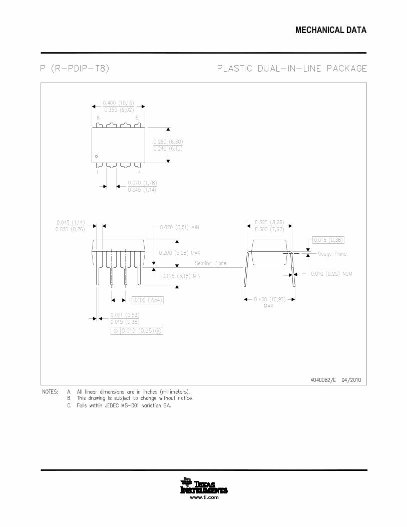
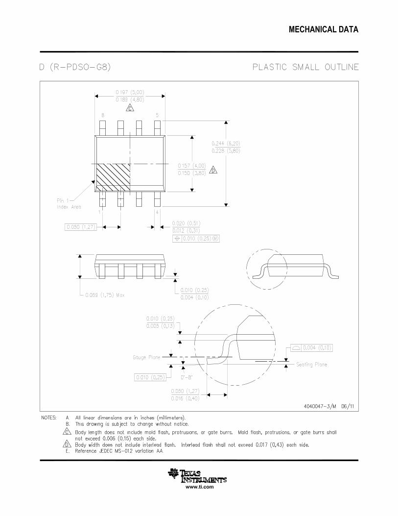
PART NUMBER PACKAGE BODY SIZE (NOM)LM7171 SOIC (8) 4.90 mm × 3.91 mmLM7171 PDIP (8) 9.81 mm × 6.35 mm
(1) For all available packages, see the orderable addendum atthe end of the datasheet.
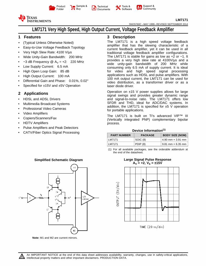
Large Signal Pulse ResponseSimplified Schematic DiagramAV = +2, VS = ±15V
Note: M1 and M2 are current mirrors.
1
An IMPORTANT NOTICE at the end of this data sheet addresses availability, warranty, changes, use in safety-critical applications,intellectual property matters and other important disclaimers. PRODUCTION DATA.
LM7171SNOS760C –MAY 1999–REVISED SEPTEMBER 2014 www.ti.com
Table of Contents7.2 Circuit Operation ..................................................... 181 Features .................................................................. 17.3 Slew Rate Characteristic......................................... 182 Applications ........................................................... 17.4 Slew Rate Limitation ............................................... 183 Description ............................................................. 17.5 Compensation For Input Capacitance .................... 194 Revision History..................................................... 27.6 Application Circuit ................................................... 195 Pin Configuration and Functions ......................... 3
8 Power Supply Recommendations ...................... 216 Specifications......................................................... 48.1 Power Supply Bypassing ........................................ 216.1 Absolute Maximum Ratings ...................................... 48.2 Termination ............................................................. 226.2 Handling Ratings....................................................... 48.3 Driving Capacitive Loads ........................................ 236.3 Recommended Operating Conditions....................... 48.4 Power Dissipation ................................................... 246.4 Thermal Information .................................................. 4
9 Layout ................................................................... 256.5 ±15V DC Electrical Characteristics .......................... 59.1 Layout Guidelines ................................................... 256.6 ±15V AC Electrical Characteristics .......................... 6
10 Device and Documentation Support ................. 266.7 ±5V DC Electrical Characteristics ............................ 710.1 Trademarks ........................................................... 266.8 ±5V AC Electrical Characteristics ............................ 810.2 Electrostatic Discharge Caution............................ 266.9 Typical Performance Characteristics ........................ 910.3 Glossary ................................................................ 267 Application and Implementation ........................ 18
11 Mechanical, Packaging, and Orderable7.1 Application Information............................................ 18Information ........................................................... 26
4 Revision HistoryNOTE: Page numbers for previous revisions may differ from page numbers in the current version.
Changes from Revision B (March 2013) to Revision C Page
• Changed data sheet flow and layout to conform with new TI standards. Added the following sections: DeviceInformation Table, Application and Implementation; Layout; Device and Documentation Support; Mechanical,Packaging, and Ordering Information .................................................................................................................................... 1
• Changed "Junction Temperature Range" to " Operating Temperature Range" and deleted TJ ............................................ 4• Deleted TJ = 25°C for Electrical Characteristics tables .......................................................................................................... 5
Changes from Revision A (March 2013) to Revision B Page
• Changed layout of National Data Sheet to TI format ........................................................................................................... 20
2 Submit Documentation Feedback Copyright © 1999–2014, Texas Instruments Incorporated
Product Folder Links: LM7171
LM7171www.ti.com SNOS760C –MAY 1999–REVISED SEPTEMBER 2014
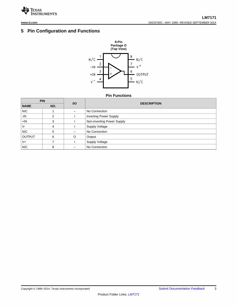
5 Pin Configuration and Functions
8-PinPackage D(Top View)
Pin FunctionsPIN
I/O DESCRIPTIONNAME NO.N/C 1 – No Connection-IN 2 I Inverting Power Supply+IN 3 I Non-inverting Power SupplyV- 4 I Supply VoltageN/C 5 – No ConnectionOUTPUT 6 O OutputV+ 7 I Supply VoltageN/C 8 – No Connection
Copyright © 1999–2014, Texas Instruments Incorporated Submit Documentation Feedback 3
Product Folder Links: LM7171
LM7171SNOS760C –MAY 1999–REVISED SEPTEMBER 2014 www.ti.com
6 Specifications
6.1 Absolute Maximum Ratingsover operating free-air temperature range (unless otherwise noted) (1)
MIN MAX UNITSupply Voltage (V+–V−) 36 VDifferential Input Voltage (2) ±10 VOutput Short Circuit to Ground (3) ContinuousMaximum Junction Temperature (4) 150 °C
(1) Stresses beyond those listed under Absolute Maximum Ratings may cause permanent damage to the device. These are stress ratingsonly, which do not imply functional operation of the device at these or any other conditions beyond those indicated under RecommendedOperating Conditions. Exposure to absolute-maximum-rated conditions for extended periods may affect device reliability.
(2) Input differential voltage is applied at VS = ±15V.(3) Applies to both single-supply and split-supply operation. Continuous short circuit operation at elevated ambient temperature can result in
exceeding the maximum allowed junction temperature of 150°C.(4) The maximum power dissipation is a function of TJ(MAX), RθJA, and TA. The maximum allowable power dissipation at any ambient
temperature is PD = (TJ(MAX)–TA)/RθJA. All numbers apply for packages soldered directly into a PC board.
6.2 Handling RatingsMIN MAX UNIT
Tstg Storage temperature range −65 +150 °CHuman body model (HBM), per ANSI/ESDA/JEDEC JS-001, all 2500V(ESD) Electrostatic discharge (1) Vpins (2)
(1) Human body model, 1.5 kΩ in series with 100 pF.(2) JEDEC document JEP155 states that 2500-V HBM allows safe manufacturing with a standard ESD control process.
6.3 Recommended Operating Conditions (1)
over operating free-air temperature range (unless otherwise noted)MIN TYP MAX UNIT
Supply Voltage 5.5V ≤ VS ≤ 36 VOperating Temperature Range: LM7171AI, LM7171BI −40 +85 °C
(1) Absolute Maximum Ratings indicate limits beyond which damage to the device may occur. Operating Ratings indicate conditions forwhich the device is intended to be functional, but specific performance is not specified. For ensured specifications and the testconditions, see the Electrical Characteristics.
6.4 Thermal InformationP (PDIP) D (SOIC)
THERMAL METRIC (1) UNIT8 PINS 8 PINS
RθJA Junction-to-ambient thermal resistance 108° 172° °C/W
(1) For more information about traditional and new thermal metrics, see the IC Package Thermal Metrics application report, SPRA953.
4 Submit Documentation Feedback Copyright © 1999–2014, Texas Instruments Incorporated
Product Folder Links: LM7171
LM7171www.ti.com SNOS760C –MAY 1999–REVISED SEPTEMBER 2014
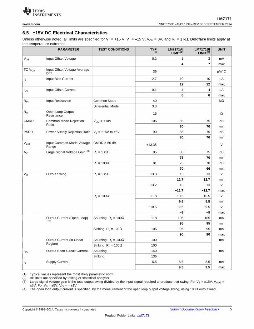
6.5 ±15V DC Electrical CharacteristicsUnless otherwise noted, all limits are specified for V+ = +15 V, V− = –15 V, VCM = 0V, and RL = 1 kΩ. Boldface limits apply atthe temperature extremes
PARAMETER TEST CONDITIONS TYP LM7171AI LM7171BI UNIT(1) LIMIT (2) LIMIT (2)
VOS Input Offset Voltage 0.2 1 3 mV4 7 max
TC VOS Input Offset Voltage Average 35 μV/°CDriftIB Input Bias Current 2.7 10 10 μA
12 12 maxIOS Input Offset Current 0.1 4 4 μA
6 6 maxRIN Input Resistance Common Mode 40 MΩ
Differential Mode 3.3RO Open Loop Output 15 ΩResistanceCMRR Common Mode Rejection VCM = ±10V 105 85 75 dB
Ratio 80 70 minPSRR Power Supply Rejection Ratio VS = ±15V to ±5V 90 85 75 dB
80 70 minVCM Input Common-Mode Voltage CMRR > 60 dB ±13.35 VRangeAV Large Signal Voltage Gain (3) RL = 1 kΩ 85 80 75 dB
75 70 minRL = 100Ω 81 75 70 dB
70 66 minVO Output Swing RL = 1 kΩ 13.3 13 13 V
12.7 12.7 min−13.2 −13 −13 V
−12.7 −12.7 maxRL = 100Ω 11.8 10.5 10.5 V
9.5 9.5 min−10.5 −9.5 −9.5 V
−9 −9 maxOutput Current (Open Loop) Sourcing, RL = 100Ω 118 105 105 mA(4)
95 95 minSinking, RL = 100Ω 105 95 95 mA
90 90 maxOutput Current (in Linear Sourcing, RL = 100Ω 100 mARegion) Sinking, RL = 100Ω 100
ISC Output Short Circuit Current Sourcing 140 mASinking 135
IS Supply Current 6.5 8.5 8.5 mA9.5 9.5 max
(1) Typical values represent the most likely parametric norm.(2) All limits are specified by testing or statistical analysis.(3) Large signal voltage gain is the total output swing divided by the input signal required to produce that swing. For VS = ±15V, VOUT =
±5V. For VS = ±5V, VOUT = ±1V.(4) The open loop output current is specified, by the measurement of the open loop output voltage swing, using 100Ω output load.
Copyright © 1999–2014, Texas Instruments Incorporated Submit Documentation Feedback 5
Product Folder Links: LM7171
LM7171SNOS760C –MAY 1999–REVISED SEPTEMBER 2014 www.ti.com
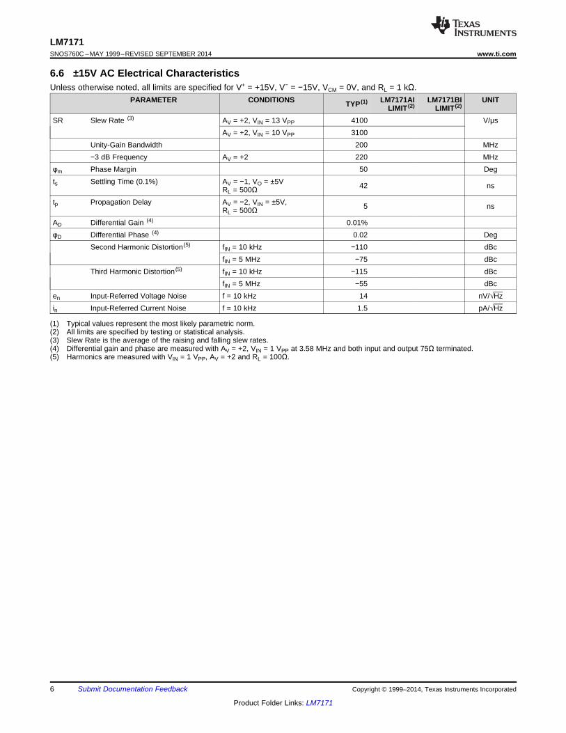
6.6 ±15V AC Electrical CharacteristicsUnless otherwise noted, all limits are specified for V+ = +15V, V− = −15V, VCM = 0V, and RL = 1 kΩ.
PARAMETER CONDITIONS LM7171AI LM7171BI UNITTYP (1)LIMIT (2) LIMIT (2)
SR Slew Rate (3) AV = +2, VIN = 13 VPP 4100 V/μsAV = +2, VIN = 10 VPP 3100
Unity-Gain Bandwidth 200 MHz−3 dB Frequency AV = +2 220 MHz
φm Phase Margin 50 Degts Settling Time (0.1%) AV = −1, VO = ±5V 42 nsRL = 500Ωtp Propagation Delay AV = −2, VIN = ±5V, 5 nsRL = 500ΩAD Differential Gain (4) 0.01%φD Differential Phase (4) 0.02 Deg
Second Harmonic Distortion (5) fIN = 10 kHz −110 dBcfIN = 5 MHz −75 dBc
Third Harmonic Distortion (5) fIN = 10 kHz −115 dBcfIN = 5 MHz −55 dBc
en Input-Referred Voltage Noise f = 10 kHz 14 nV/√Hzin Input-Referred Current Noise f = 10 kHz 1.5 pA/√Hz
(1) Typical values represent the most likely parametric norm.(2) All limits are specified by testing or statistical analysis.(3) Slew Rate is the average of the raising and falling slew rates.(4) Differential gain and phase are measured with AV = +2, VIN = 1 VPP at 3.58 MHz and both input and output 75Ω terminated.(5) Harmonics are measured with VIN = 1 VPP, AV = +2 and RL = 100Ω.
6 Submit Documentation Feedback Copyright © 1999–2014, Texas Instruments Incorporated
Product Folder Links: LM7171
LM7171www.ti.com SNOS760C –MAY 1999–REVISED SEPTEMBER 2014
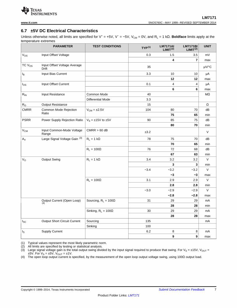
6.7 ±5V DC Electrical CharacteristicsUnless otherwise noted, all limits are specified for V+ = +5V, V− = −5V, VCM = 0V, and RL = 1 kΩ. Boldface limits apply at thetemperature extremes
PARAMETER TEST CONDITIONS LM7171AI LM7171BI UNITTYP (1)LIMIT (2) LIMIT (2)
VOS Input Offset Voltage 0.3 1.5 3.5 mV4 7 max
TC VOS Input Offset Voltage Average 35 μV/°CDriftIB Input Bias Current 3.3 10 10 μA
12 12 maxIOS Input Offset Current 0.1 4 4 μA
6 6 maxRIN Input Resistance Common Mode 40 MΩ
Differential Mode 3.3RO Output Resistance 15 ΩCMRR Common Mode Rejection VCM = ±2.5V 104 80 70 dB
Ratio 75 65 minPSRR Power Supply Rejection Ratio VS = ±15V to ±5V 90 85 75 dB
80 70 minVCM Input Common-Mode Voltage CMRR > 60 dB ±3.2 VRangeAV Large Signal Voltage Gain (3) RL = 1 kΩ 78 75 70 dB
70 65 minRL = 100Ω 76 72 68 dB
67 63 minVO Output Swing RL = 1 kΩ 3.4 3.2 3.2 V
3 3 min−3.4 −3.2 −3.2 V
−3 −3 maxRL = 100Ω 3.1 2.9 2.9 V
2.8 2.8 min−3.0 −2.9 −2.9 V
−2.8 −2.8 maxOutput Current (Open Loop) Sourcing, RL = 100Ω 31 29 29 mA(4)
28 28 minSinking, RL = 100Ω 30 29 29 mA
28 28 maxISC Output Short Circuit Current Sourcing 135 mA
Sinking 100IS Supply Current 6.2 8 8 mA
9 9 max
(1) Typical values represent the most likely parametric norm.(2) All limits are specified by testing or statistical analysis.(3) Large signal voltage gain is the total output swing divided by the input signal required to produce that swing. For VS = ±15V, VOUT =
±5V. For VS = ±5V, VOUT = ±1V.(4) The open loop output current is specified, by the measurement of the open loop output voltage swing, using 100Ω output load.
Copyright © 1999–2014, Texas Instruments Incorporated Submit Documentation Feedback 7
Product Folder Links: LM7171
LM7171SNOS760C –MAY 1999–REVISED SEPTEMBER 2014 www.ti.com
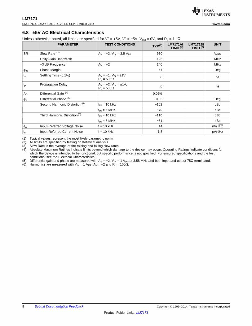
6.8 ±5V AC Electrical CharacteristicsUnless otherwise noted, all limits are specified for V+ = +5V, V− = −5V, VCM = 0V, and RL = 1 kΩ.
PARAMETER TEST CONDITIONS LM7171AI LM7171BI UNITTYP (1)LIMIT (2) LIMIT (2)
SR Slew Rate (3) AV = +2, VIN = 3.5 VPP 950 V/μsUnity-Gain Bandwidth 125 MHz−3 dB Frequency AV = +2 140 MHz
φm Phase Margin 57 Degts Settling Time (0.1%) AV = −1, VO = ±1V, 56 nsRL = 500Ωtp Propagation Delay AV = −2, VIN = ±1V, 6 nsRL = 500ΩAD Differential Gain (4) 0.02%φD Differential Phase (5) 0.03 Deg
Second Harmonic Distortion (6) fIN = 10 kHz −102 dBcfIN = 5 MHz −70 dBc
Third Harmonic Distortion (6) fIN = 10 kHz −110 dBcfIN = 5 MHz −51 dBc
en Input-Referred Voltage Noise f = 10 kHz 14 nV/√Hzin Input-Referred Current Noise f = 10 kHz 1.8 pA/√Hz
(1) Typical values represent the most likely parametric norm.(2) All limits are specified by testing or statistical analysis.(3) Slew Rate is the average of the raising and falling slew rates.(4) Absolute Maximum Ratings indicate limits beyond which damage to the device may occur. Operating Ratings indicate conditions for
which the device is intended to be functional, but specific performance is not specified. For ensured specifications and the testconditions, see the Electrical Characteristics.
(5) Differential gain and phase are measured with AV = +2, VIN = 1 VPP at 3.58 MHz and both input and output 75Ω terminated.(6) Harmonics are measured with VIN = 1 VPP, AV = +2 and RL = 100Ω.
8 Submit Documentation Feedback Copyright © 1999–2014, Texas Instruments Incorporated
Product Folder Links: LM7171
LM7171www.ti.com SNOS760C –MAY 1999–REVISED SEPTEMBER 2014
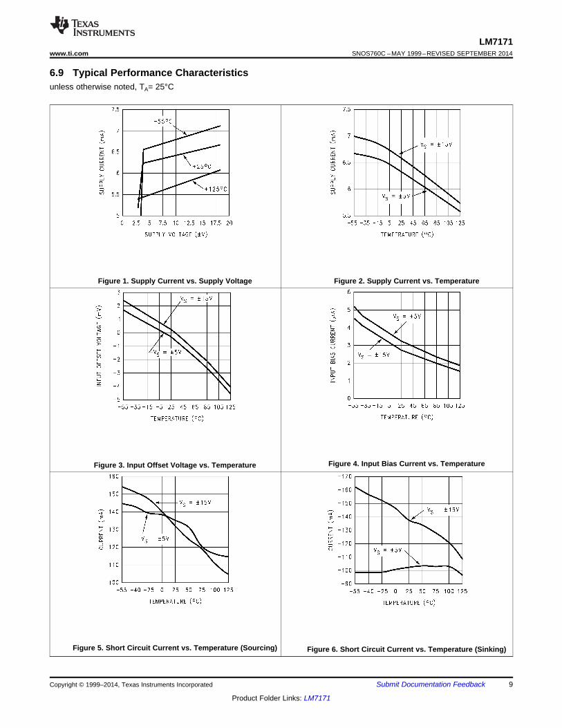
6.9 Typical Performance Characteristicsunless otherwise noted, TA= 25°C
Figure 1. Supply Current vs. Supply Voltage Figure 2. Supply Current vs. Temperature
Figure 4. Input Bias Current vs. TemperatureFigure 3. Input Offset Voltage vs. Temperature
Figure 5. Short Circuit Current vs. Temperature (Sourcing) Figure 6. Short Circuit Current vs. Temperature (Sinking)
Copyright © 1999–2014, Texas Instruments Incorporated Submit Documentation Feedback 9
Product Folder Links: LM7171
LM7171SNOS760C –MAY 1999–REVISED SEPTEMBER 2014 www.ti.com
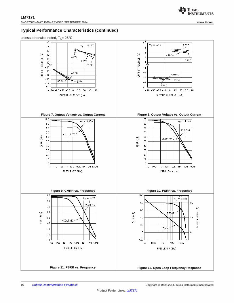
Typical Performance Characteristics (continued)unless otherwise noted, TA= 25°C
Figure 7. Output Voltage vs. Output Current Figure 8. Output Voltage vs. Output Current
Figure 9. CMRR vs. Frequency Figure 10. PSRR vs. Frequency
Figure 11. PSRR vs. Frequency Figure 12. Open Loop Frequency Response
10 Submit Documentation Feedback Copyright © 1999–2014, Texas Instruments Incorporated
Product Folder Links: LM7171
LM7171www.ti.com SNOS760C –MAY 1999–REVISED SEPTEMBER 2014
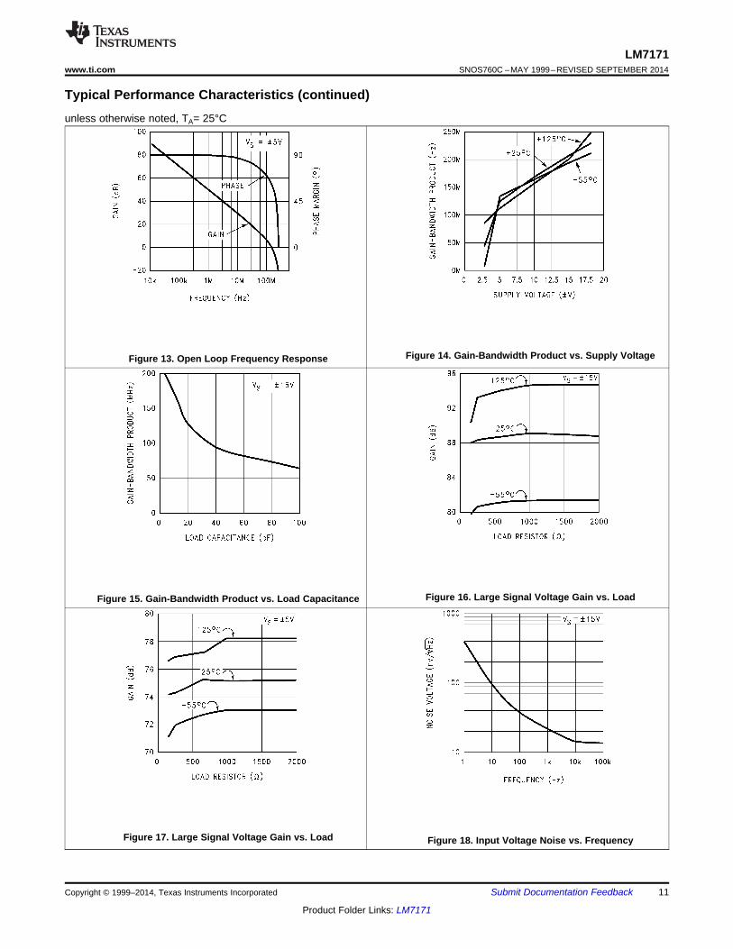
Typical Performance Characteristics (continued)unless otherwise noted, TA= 25°C
Figure 14. Gain-Bandwidth Product vs. Supply VoltageFigure 13. Open Loop Frequency Response
Figure 16. Large Signal Voltage Gain vs. LoadFigure 15. Gain-Bandwidth Product vs. Load Capacitance
Figure 17. Large Signal Voltage Gain vs. Load Figure 18. Input Voltage Noise vs. Frequency
Copyright © 1999–2014, Texas Instruments Incorporated Submit Documentation Feedback 11
Product Folder Links: LM7171
LM7171SNOS760C –MAY 1999–REVISED SEPTEMBER 2014 www.ti.com
Typical Performance Characteristics (continued)unless otherwise noted, TA= 25°C
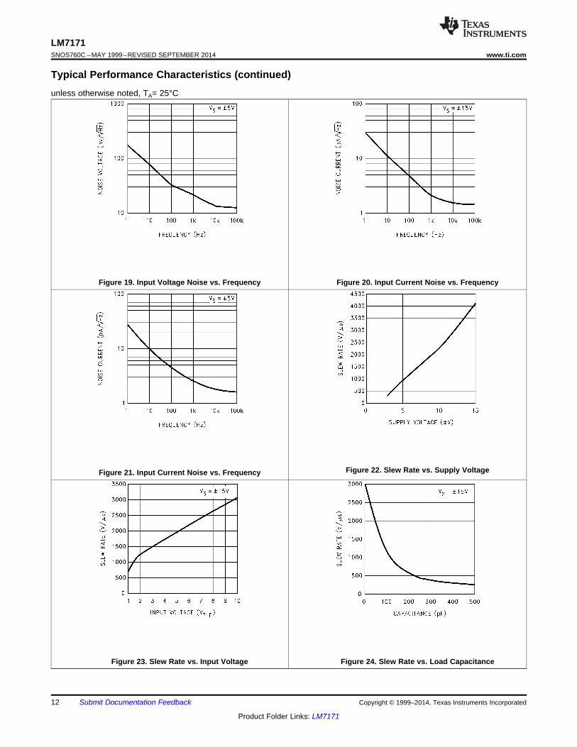
Figure 19. Input Voltage Noise vs. Frequency Figure 20. Input Current Noise vs. Frequency
Figure 22. Slew Rate vs. Supply VoltageFigure 21. Input Current Noise vs. Frequency
Figure 23. Slew Rate vs. Input Voltage Figure 24. Slew Rate vs. Load Capacitance
12 Submit Documentation Feedback Copyright © 1999–2014, Texas Instruments Incorporated
Product Folder Links: LM7171
LM7171www.ti.com SNOS760C –MAY 1999–REVISED SEPTEMBER 2014
Typical Performance Characteristics (continued)unless otherwise noted, TA= 25°C
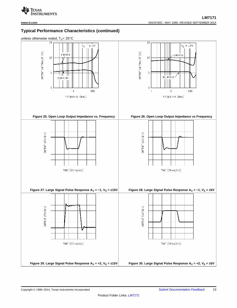
Figure 25. Open Loop Output Impedance vs. Frequency Figure 26. Open Loop Output Impedance vs Frequency
Figure 27. Large Signal Pulse Response AV = −1, VS = ±15V Figure 28. Large Signal Pulse Response AV = −1, VS = ±5V
Figure 29. Large Signal Pulse Response AV = +2, VS = ±15V Figure 30. Large Signal Pulse Response AV = +2, VS = ±5V
Copyright © 1999–2014, Texas Instruments Incorporated Submit Documentation Feedback 13
Product Folder Links: LM7171
LM7171SNOS760C –MAY 1999–REVISED SEPTEMBER 2014 www.ti.com
Typical Performance Characteristics (continued)unless otherwise noted, TA= 25°C
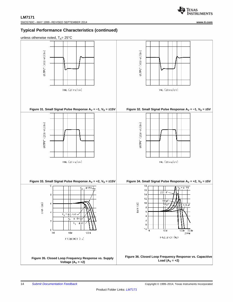
Figure 31. Small Signal Pulse Response AV = −1, VS = ±15V Figure 32. Small Signal Pulse Response AV = −1, VS = ±5V
Figure 33. Small Signal Pulse Response AV = +2, VS = ±15V Figure 34. Small Signal Pulse Response AV = +2, VS = ±5V
Figure 36. Closed Loop Frequency Response vs. CapacitiveFigure 35. Closed Loop Frequency Response vs. SupplyLoad (AV = +2)Voltage (AV = +2)
14 Submit Documentation Feedback Copyright © 1999–2014, Texas Instruments Incorporated
Product Folder Links: LM7171
LM7171www.ti.com SNOS760C –MAY 1999–REVISED SEPTEMBER 2014
Typical Performance Characteristics (continued)unless otherwise noted, TA= 25°C
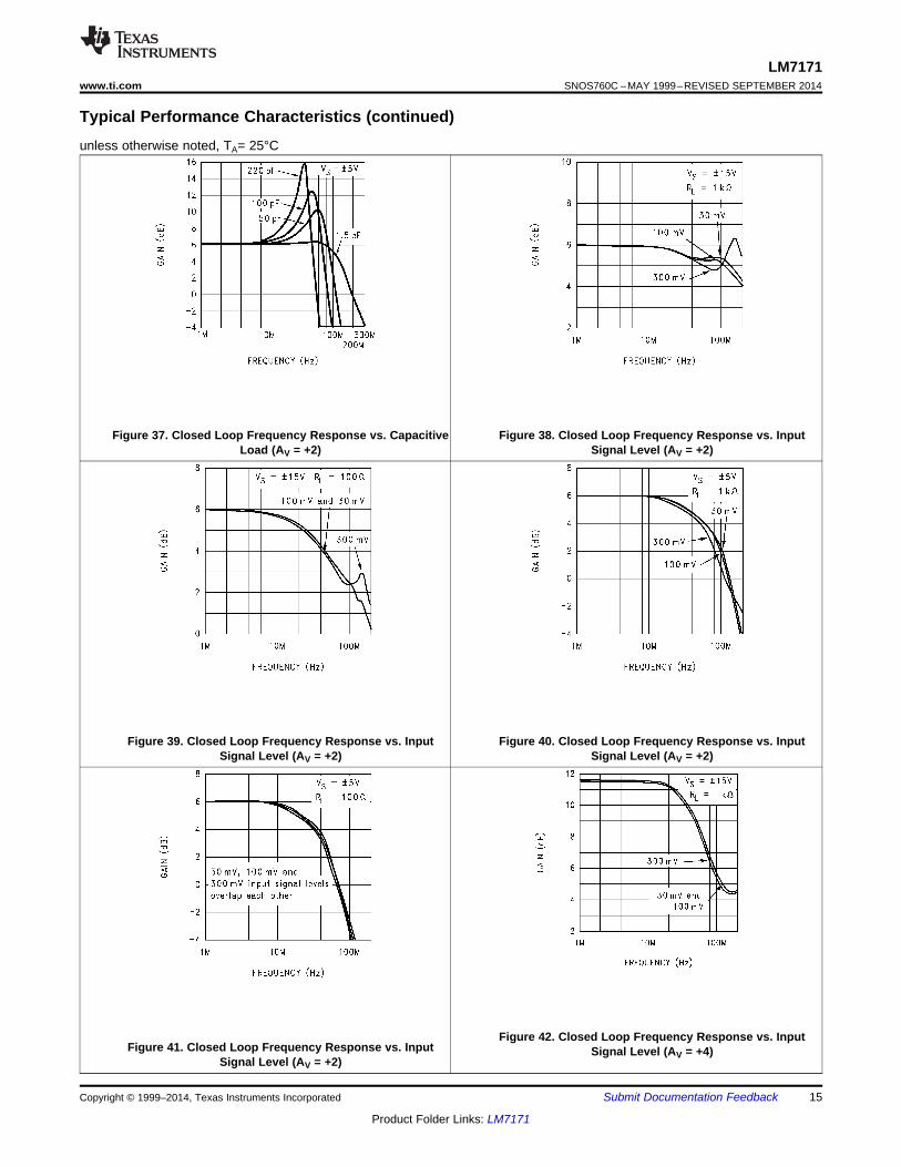
Figure 37. Closed Loop Frequency Response vs. Capacitive Figure 38. Closed Loop Frequency Response vs. InputLoad (AV = +2) Signal Level (AV = +2)
Figure 39. Closed Loop Frequency Response vs. Input Figure 40. Closed Loop Frequency Response vs. InputSignal Level (AV = +2) Signal Level (AV = +2)
Figure 42. Closed Loop Frequency Response vs. InputFigure 41. Closed Loop Frequency Response vs. Input Signal Level (AV = +4)
Signal Level (AV = +2)
Copyright © 1999–2014, Texas Instruments Incorporated Submit Documentation Feedback 15
Product Folder Links: LM7171
LM7171SNOS760C –MAY 1999–REVISED SEPTEMBER 2014 www.ti.com
Typical Performance Characteristics (continued)unless otherwise noted, TA= 25°C
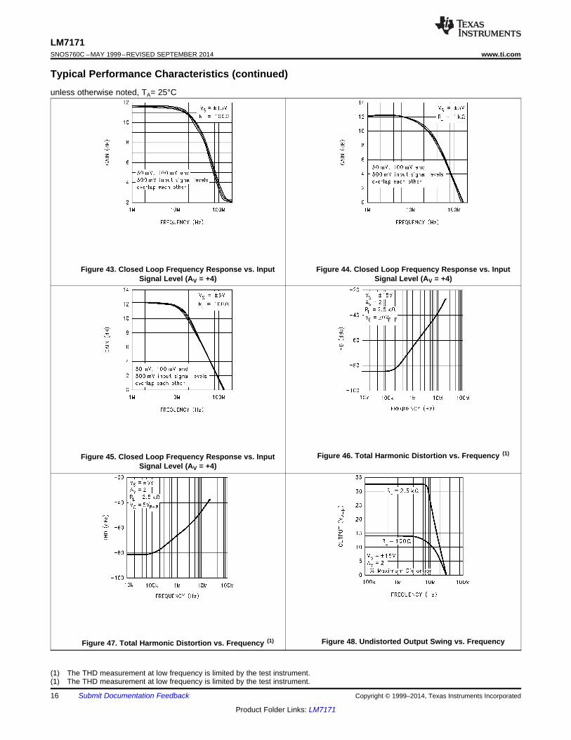
Figure 43. Closed Loop Frequency Response vs. Input Figure 44. Closed Loop Frequency Response vs. InputSignal Level (AV = +4) Signal Level (AV = +4)
Figure 46. Total Harmonic Distortion vs. Frequency (1)Figure 45. Closed Loop Frequency Response vs. InputSignal Level (AV = +4)
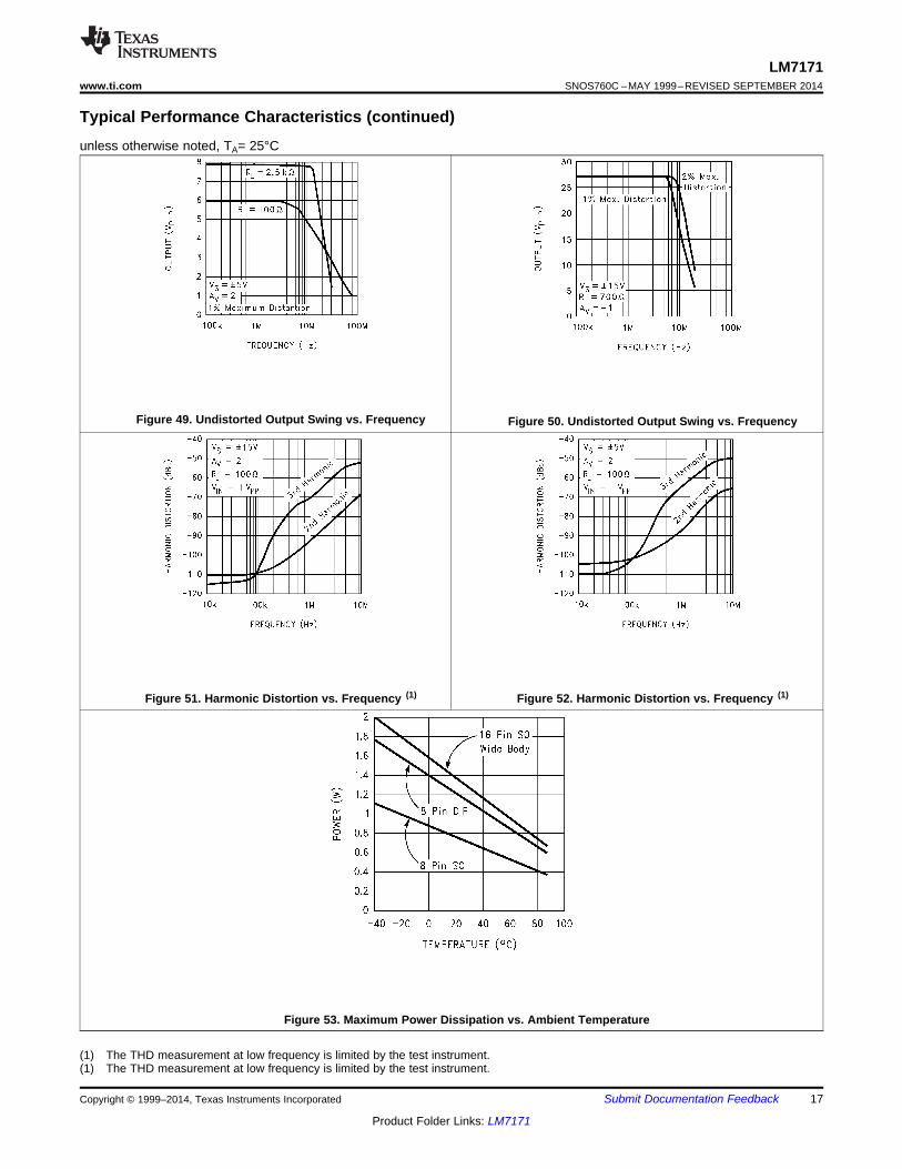
Figure 48. Undistorted Output Swing vs. FrequencyFigure 47. Total Harmonic Distortion vs. Frequency (1)
(1) The THD measurement at low frequency is limited by the test instrument.(1) The THD measurement at low frequency is limited by the test instrument.
16 Submit Documentation Feedback Copyright © 1999–2014, Texas Instruments Incorporated
Product Folder Links: LM7171
LM7171www.ti.com SNOS760C –MAY 1999–REVISED SEPTEMBER 2014
Typical Performance Characteristics (continued)unless otherwise noted, TA= 25°C
Figure 49. Undistorted Output Swing vs. Frequency Figure 50. Undistorted Output Swing vs. Frequency
Figure 51. Harmonic Distortion vs. Frequency (1) Figure 52. Harmonic Distortion vs. Frequency (1)
Figure 53. Maximum Power Dissipation vs. Ambient Temperature
(1) The THD measurement at low frequency is limited by the test instrument.(1) The THD measurement at low frequency is limited by the test instrument.
Copyright © 1999–2014, Texas Instruments Incorporated Submit Documentation Feedback 17
Product Folder Links: LM7171
LM7171SNOS760C –MAY 1999–REVISED SEPTEMBER 2014 www.ti.com
7 Application and Implementation
7.1 Application InformationThe LM7171 is a very high speed, voltage feedback amplifier. It consumes only 6.5 mA supply current whileproviding a unity-gain bandwidth of 200 MHz and a slew rate of 4100V/μs. It also has other great features suchas low differential gain and phase and high output current.
The LM7171 is a true voltage feedback amplifier. Unlike current feedback amplifiers (CFAs) with a low invertinginput impedance and a high non-inverting input impedance, both inputs of voltage feedback amplifiers (VFAs)have high impedance nodes. The low impedance inverting input in CFAs and a feedback capacitor create anadditional pole that will lead to instability. As a result, CFAs cannot be used in traditional op amp circuits such asphotodiode amplifiers, I-to-V converters and integrators where a feedback capacitor is required.
7.2 Circuit OperationThe class AB input stage in LM7171 is fully symmetrical and has a similar slewing characteristic to the currentfeedback amplifiers. In the LM7171 Simplified Schematic, Q1 through Q4 form the equivalent of the currentfeedback input buffer, RE the equivalent of the feedback resistor, and stage A buffers the inverting input. Thetriple-buffered output stage isolates the gain stage from the load to provide low output impedance.
7.3 Slew Rate CharacteristicThe slew rate of LM7171 is determined by the current available to charge and discharge an internal highimpedance node capacitor. This current is the differential input voltage divided by the total degeneration resistorRE. Therefore, the slew rate is proportional to the input voltage level, and the higher slew rates are achievable inthe lower gain configurations. A curve of slew rate versus input voltage level is provided in Typical PerformanceCharacteristics
When a very fast large signal pulse is applied to the input of an amplifier, some overshoot or undershoot occurs.By placing an external resistor such as 1 kΩ in series with the input of LM7171, the bandwidth is reduced to helplower the overshoot.
7.4 Slew Rate LimitationIf the amplifier's input signal has too large of an amplitude at too high of a frequency, the amplifier is said to beslew rate limited; this can cause ringing in time domain and peaking in frequency domain at the output of theamplifier.
In Typical Performance Characteristics, there are several curves of AV = +2 and AV = +4 versus input signallevels. For the AV = +4 curves, no peaking is present and the LM7171 responds identically to the different inputsignal levels of 30 mV, 100 mV and 300 mV.
For the AV = +2 curves, with slight peaking occurs. This peaking at high frequency (>100 MHz) is caused by alarge input signal at high enough frequency that exceeds the amplifier's slew rate. The peaking in frequencyresponse does not limit the pulse response in time domain, and the LM7171 is stable with noise gain of ≥+2.
18 Submit Documentation Feedback Copyright © 1999–2014, Texas Instruments Incorporated
Product Folder Links: LM7171
LM7171www.ti.com SNOS760C –MAY 1999–REVISED SEPTEMBER 2014
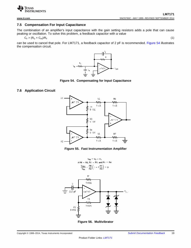
7.5 Compensation For Input CapacitanceThe combination of an amplifier's input capacitance with the gain setting resistors adds a pole that can causepeaking or oscillation. To solve this problem, a feedback capacitor with a value
CF > (RG × CIN)/RF (1)
can be used to cancel that pole. For LM7171, a feedback capacitor of 2 pF is recommended. Figure 54 illustratesthe compensation circuit.
Figure 54. Compensating for Input Capacitance
7.6 Application Circuit
Figure 55. Fast Instrumentation Amplifier
Figure 56. Multivibrator
Copyright © 1999–2014, Texas Instruments Incorporated Submit Documentation Feedback 19
Product Folder Links: LM7171

LM7171SNOS760C –MAY 1999–REVISED SEPTEMBER 2014 www.ti.com
Application Circuit (continued)
Figure 57. Pulse Width Modulator
Figure 58. Video Line Driver
20 Submit Documentation Feedback Copyright © 1999–2014, Texas Instruments Incorporated
Product Folder Links: LM7171
LM7171www.ti.com SNOS760C –MAY 1999–REVISED SEPTEMBER 2014
8 Power Supply Recommendations
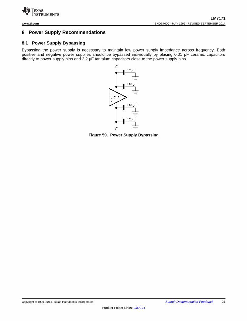
8.1 Power Supply BypassingBypassing the power supply is necessary to maintain low power supply impedance across frequency. Bothpositive and negative power supplies should be bypassed individually by placing 0.01 μF ceramic capacitorsdirectly to power supply pins and 2.2 μF tantalum capacitors close to the power supply pins.
Figure 59. Power Supply Bypassing
Copyright © 1999–2014, Texas Instruments Incorporated Submit Documentation Feedback 21
Product Folder Links: LM7171
LM7171SNOS760C –MAY 1999–REVISED SEPTEMBER 2014 www.ti.com
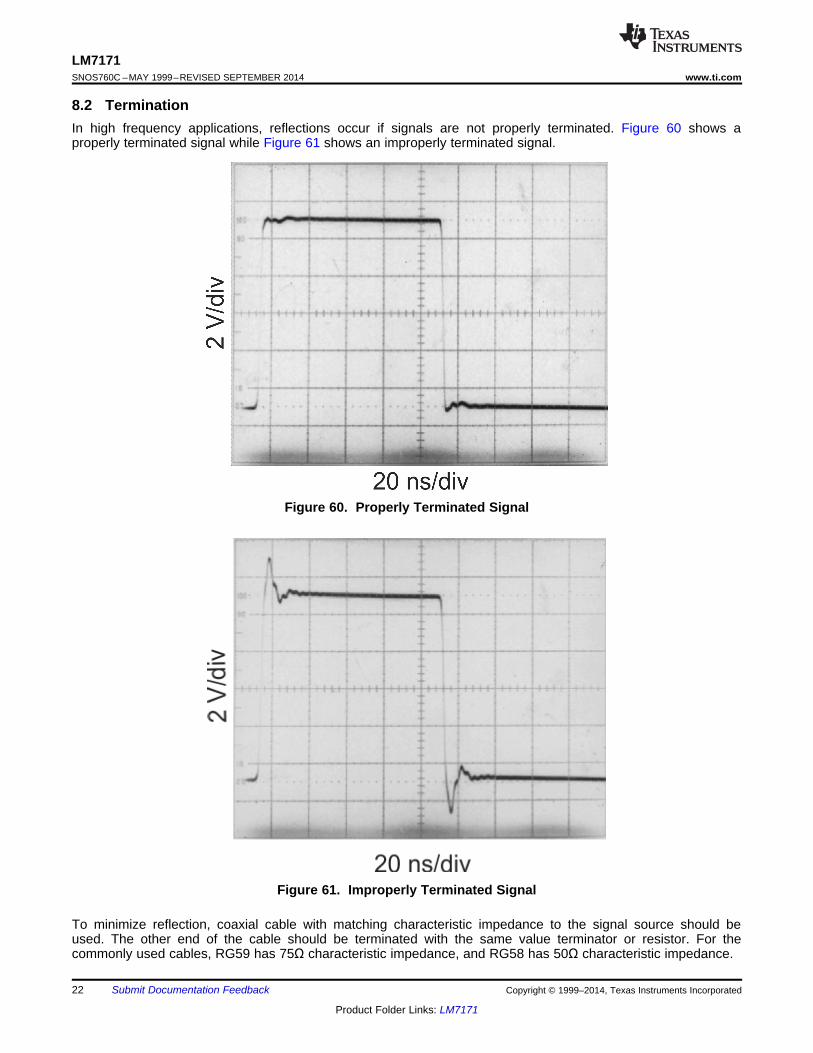
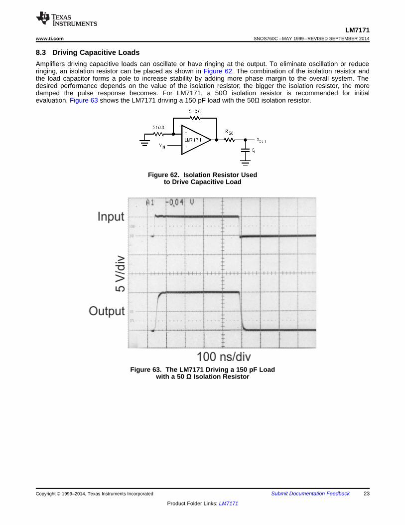
8.2 TerminationIn high frequency applications, reflections occur if signals are not properly terminated. Figure 60 shows aproperly terminated signal while Figure 61 shows an improperly terminated signal.
Figure 60. Properly Terminated Signal
Figure 61. Improperly Terminated Signal
To minimize reflection, coaxial cable with matching characteristic impedance to the signal source should beused. The other end of the cable should be terminated with the same value terminator or resistor. For thecommonly used cables, RG59 has 75Ω characteristic impedance, and RG58 has 50Ω characteristic impedance.
22 Submit Documentation Feedback Copyright © 1999–2014, Texas Instruments Incorporated
Product Folder Links: LM7171
LM7171www.ti.com SNOS760C –MAY 1999–REVISED SEPTEMBER 2014
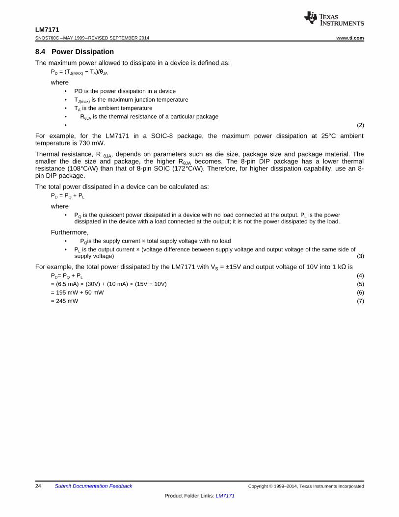
8.3 Driving Capacitive LoadsAmplifiers driving capacitive loads can oscillate or have ringing at the output. To eliminate oscillation or reduceringing, an isolation resistor can be placed as shown in Figure 62. The combination of the isolation resistor andthe load capacitor forms a pole to increase stability by adding more phase margin to the overall system. Thedesired performance depends on the value of the isolation resistor; the bigger the isolation resistor, the moredamped the pulse response becomes. For LM7171, a 50Ω isolation resistor is recommended for initialevaluation. Figure 63 shows the LM7171 driving a 150 pF load with the 50Ω isolation resistor.
Figure 62. Isolation Resistor Usedto Drive Capacitive Load
Figure 63. The LM7171 Driving a 150 pF Loadwith a 50 Ω Isolation Resistor
Copyright © 1999–2014, Texas Instruments Incorporated Submit Documentation Feedback 23
Product Folder Links: LM7171
LM7171SNOS760C –MAY 1999–REVISED SEPTEMBER 2014 www.ti.com
8.4 Power DissipationThe maximum power allowed to dissipate in a device is defined as:
PD = (TJ(MAX) − TA)/θJA
where• PD is the power dissipation in a device• TJ(max) is the maximum junction temperature• TA is the ambient temperature• RθJA is the thermal resistance of a particular package• (2)
For example, for the LM7171 in a SOIC-8 package, the maximum power dissipation at 25°C ambienttemperature is 730 mW.
Thermal resistance, R θJA, depends on parameters such as die size, package size and package material. Thesmaller the die size and package, the higher RθJA becomes. The 8-pin DIP package has a lower thermalresistance (108°C/W) than that of 8-pin SOIC (172°C/W). Therefore, for higher dissipation capability, use an 8-pin DIP package.
The total power dissipated in a device can be calculated as:PD = PQ + PL
where• PQ is the quiescent power dissipated in a device with no load connected at the output. PL is the power
dissipated in the device with a load connected at the output; it is not the power dissipated by the load.
Furthermore,• PQis the supply current × total supply voltage with no load• PL is the output current × (voltage difference between supply voltage and output voltage of the same side of
supply voltage) (3)
For example, the total power dissipated by the LM7171 with VS = ±15V and output voltage of 10V into 1 kΩ isPD= PQ + PL (4)= (6.5 mA) × (30V) + (10 mA) × (15V − 10V) (5)= 195 mW + 50 mW (6)= 245 mW (7)
24 Submit Documentation Feedback Copyright © 1999–2014, Texas Instruments Incorporated
Product Folder Links: LM7171
LM7171www.ti.com SNOS760C –MAY 1999–REVISED SEPTEMBER 2014
9 Layout
9.1 Layout Guidelines
9.1.1 Printed Circuit Board and High Speed Op AmpsThere are many things to consider when designing PC boards for high speed op amps. Without proper caution, itis very easy to have excessive ringing, oscillation and other degraded AC performance in high speed circuits. Asa rule, the signal traces should be short and wide to provide low inductance and low impedance paths. Anyunused board space needs to be grounded to reduce stray signal pickup. Critical components should also begrounded at a common point to eliminate voltage drop. Sockets add capacitance to the board and can affect highfrequency performance. It is better to solder the amplifier directly into the PC board without using any socket.
9.1.2 Using ProbesActive (FET) probes are ideal for taking high frequency measurements because they have wide bandwidth, highinput impedance and low input capacitance. However, the probe ground leads provide a long ground loop thatwill produce errors in measurement. Instead, the probes can be grounded directly by removing the ground leadsand probe jackets and using scope probe jacks.
9.1.3 Component Selection and Feedback ResistorIt is important in high speed applications to keep all component leads short. For discrete components, choosecarbon composition-type resistors and mica-type capacitors. Surface mount components are preferred overdiscrete components for minimum inductive effect.
Large values of feedback resistors can couple with parasitic capacitance and cause undesirable effects such asringing or oscillation in high speed amplifiers. For LM7171, a feedback resistor of 510Ω gives optimalperformance.
Copyright © 1999–2014, Texas Instruments Incorporated Submit Documentation Feedback 25
Product Folder Links: LM7171
LM7171SNOS760C –MAY 1999–REVISED SEPTEMBER 2014 www.ti.com
10 Device and Documentation Support
10.1 TrademarksVIP is a trademark of Texas Instruments.All other trademarks are the property of their respective owners.
10.2 Electrostatic Discharge CautionThese devices have limited built-in ESD protection. The leads should be shorted together or the device placed in conductive foamduring storage or handling to prevent electrostatic damage to the MOS gates.
10.3 GlossarySLYZ022 — TI Glossary.
This glossary lists and explains terms, acronyms, and definitions.
11 Mechanical, Packaging, and Orderable InformationThe following pages include mechanical, packaging, and orderable information. This information is the mostcurrent data available for the designated devices. This data is subject to change without notice and revision ofthis document. For browser-based versions of this data sheet, refer to the left-hand navigation.
26 Submit Documentation Feedback Copyright © 1999–2014, Texas Instruments Incorporated
Product Folder Links: LM7171
PACKAGE OPTION ADDENDUM
www.ti.com 19-Mar-2015
Addendum-Page 1
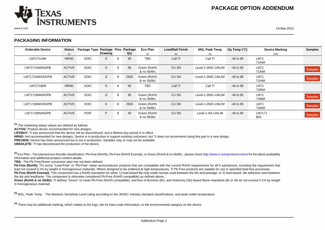
PACKAGING INFORMATION
Orderable Device Status(1)
Package Type PackageDrawing
Pins PackageQty
Eco Plan(2)
Lead/Ball Finish(6)
MSL Peak Temp(3)
Op Temp (°C) Device Marking(4/5)
Samples
LM7171AIM NRND SOIC D 8 95 TBD Call TI Call TI -40 to 85 LM7171AIM
LM7171AIM/NOPB ACTIVE SOIC D 8 95 Green (RoHS& no Sb/Br)
CU SN Level-1-260C-UNLIM -40 to 85 LM7171AIM
LM7171AIMX/NOPB ACTIVE SOIC D 8 2500 Green (RoHS& no Sb/Br)
CU SN Level-1-260C-UNLIM -40 to 85 LM7171AIM
LM7171BIM NRND SOIC D 8 95 TBD Call TI Call TI -40 to 85 LM7171BIM
LM7171BIM/NOPB ACTIVE SOIC D 8 95 Green (RoHS& no Sb/Br)
CU SN Level-1-260C-UNLIM -40 to 85 LM7171BIM
LM7171BIMX/NOPB ACTIVE SOIC D 8 2500 Green (RoHS& no Sb/Br)
CU SN Level-1-260C-UNLIM -40 to 85 LM7171BIM
LM7171BIN/NOPB ACTIVE PDIP P 8 40 Green (RoHS& no Sb/Br)
CU SN Level-1-NA-UNLIM -40 to 85 LM7171BIN
(1) The marketing status values are defined as follows:ACTIVE: Product device recommended for new designs.LIFEBUY: TI has announced that the device will be discontinued, and a lifetime-buy period is in effect.NRND: Not recommended for new designs. Device is in production to support existing customers, but TI does not recommend using this part in a new design.PREVIEW: Device has been announced but is not in production. Samples may or may not be available.OBSOLETE: TI has discontinued the production of the device.
(2) Eco Plan - The planned eco-friendly classification: Pb-Free (RoHS), Pb-Free (RoHS Exempt), or Green (RoHS & no Sb/Br) - please check http://www.ti.com/productcontent for the latest availabilityinformation and additional product content details.TBD: The Pb-Free/Green conversion plan has not been defined.Pb-Free (RoHS): TI's terms "Lead-Free" or "Pb-Free" mean semiconductor products that are compatible with the current RoHS requirements for all 6 substances, including the requirement thatlead not exceed 0.1% by weight in homogeneous materials. Where designed to be soldered at high temperatures, TI Pb-Free products are suitable for use in specified lead-free processes.Pb-Free (RoHS Exempt): This component has a RoHS exemption for either 1) lead-based flip-chip solder bumps used between the die and package, or 2) lead-based die adhesive used betweenthe die and leadframe. The component is otherwise considered Pb-Free (RoHS compatible) as defined above.Green (RoHS & no Sb/Br): TI defines "Green" to mean Pb-Free (RoHS compatible), and free of Bromine (Br) and Antimony (Sb) based flame retardants (Br or Sb do not exceed 0.1% by weightin homogeneous material)
(3) MSL, Peak Temp. - The Moisture Sensitivity Level rating according to the JEDEC industry standard classifications, and peak solder temperature.
(4) There may be additional marking, which relates to the logo, the lot trace code information, or the environmental category on the device.
PACKAGE OPTION ADDENDUM
www.ti.com 19-Mar-2015
Addendum-Page 2
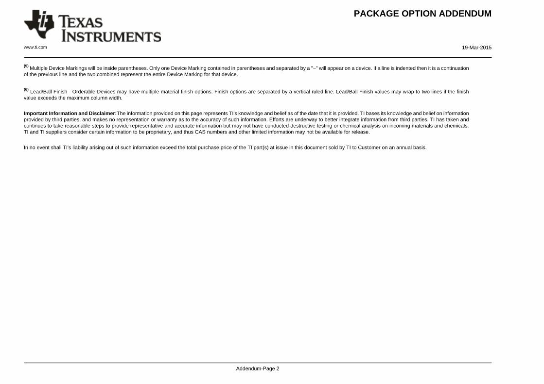
(5) Multiple Device Markings will be inside parentheses. Only one Device Marking contained in parentheses and separated by a "~" will appear on a device. If a line is indented then it is a continuationof the previous line and the two combined represent the entire Device Marking for that device.
(6) Lead/Ball Finish - Orderable Devices may have multiple material finish options. Finish options are separated by a vertical ruled line. Lead/Ball Finish values may wrap to two lines if the finishvalue exceeds the maximum column width.
Important Information and Disclaimer:The information provided on this page represents TI's knowledge and belief as of the date that it is provided. TI bases its knowledge and belief on informationprovided by third parties, and makes no representation or warranty as to the accuracy of such information. Efforts are underway to better integrate information from third parties. TI has taken andcontinues to take reasonable steps to provide representative and accurate information but may not have conducted destructive testing or chemical analysis on incoming materials and chemicals.TI and TI suppliers consider certain information to be proprietary, and thus CAS numbers and other limited information may not be available for release.
In no event shall TI's liability arising out of such information exceed the total purchase price of the TI part(s) at issue in this document sold by TI to Customer on an annual basis.
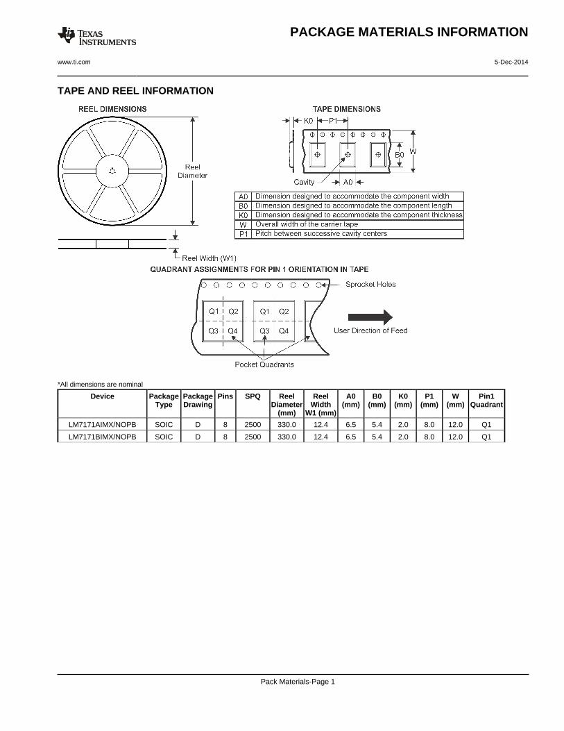
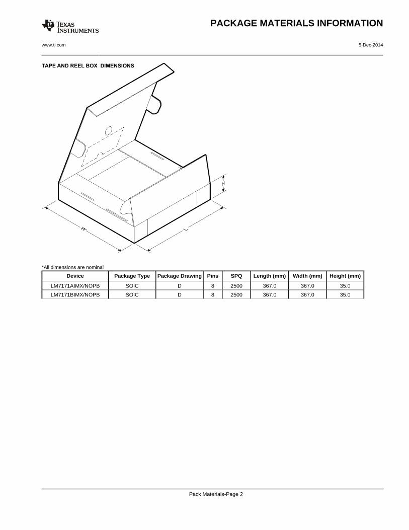
TAPE AND REEL INFORMATION
*All dimensions are nominal
Device PackageType
PackageDrawing
Pins SPQ ReelDiameter
(mm)
ReelWidth
W1 (mm)
A0(mm)
B0(mm)
K0(mm)
P1(mm)
W(mm)
Pin1Quadrant
LM7171AIMX/NOPB SOIC D 8 2500 330.0 12.4 6.5 5.4 2.0 8.0 12.0 Q1
LM7171BIMX/NOPB SOIC D 8 2500 330.0 12.4 6.5 5.4 2.0 8.0 12.0 Q1
PACKAGE MATERIALS INFORMATION
www.ti.com 5-Dec-2014
Pack Materials-Page 1
*All dimensions are nominal
Device Package Type Package Drawing Pins SPQ Length (mm) Width (mm) Height (mm)
LM7171AIMX/NOPB SOIC D 8 2500 367.0 367.0 35.0
LM7171BIMX/NOPB SOIC D 8 2500 367.0 367.0 35.0
PACKAGE MATERIALS INFORMATION
www.ti.com 5-Dec-2014
Pack Materials-Page 2
IMPORTANT NOTICE
Texas Instruments Incorporated and its subsidiaries (TI) reserve the right to make corrections, enhancements, improvements and otherchanges to its semiconductor products and services per JESD46, latest issue, and to discontinue any product or service per JESD48, latestissue. Buyers should obtain the latest relevant information before placing orders and should verify that such information is current andcomplete. All semiconductor products (also referred to herein as “components”) are sold subject to TI’s terms and conditions of salesupplied at the time of order acknowledgment.TI warrants performance of its components to the specifications applicable at the time of sale, in accordance with the warranty in TI’s termsand conditions of sale of semiconductor products. Testing and other quality control techniques are used to the extent TI deems necessaryto support this warranty. Except where mandated by applicable law, testing of all parameters of each component is not necessarilyperformed.TI assumes no liability for applications assistance or the design of Buyers’ products. Buyers are responsible for their products andapplications using TI components. To minimize the risks associated with Buyers’ products and applications, Buyers should provideadequate design and operating safeguards.TI does not warrant or represent that any license, either express or implied, is granted under any patent right, copyright, mask work right, orother intellectual property right relating to any combination, machine, or process in which TI components or services are used. Informationpublished by TI regarding third-party products or services does not constitute a license to use such products or services or a warranty orendorsement thereof. Use of such information may require a license from a third party under the patents or other intellectual property of thethird party, or a license from TI under the patents or other intellectual property of TI.Reproduction of significant portions of TI information in TI data books or data sheets is permissible only if reproduction is without alterationand is accompanied by all associated warranties, conditions, limitations, and notices. TI is not responsible or liable for such altereddocumentation. Information of third parties may be subject to additional restrictions.Resale of TI components or services with statements different from or beyond the parameters stated by TI for that component or servicevoids all express and any implied warranties for the associated TI component or service and is an unfair and deceptive business practice.TI is not responsible or liable for any such statements.Buyer acknowledges and agrees that it is solely responsible for compliance with all legal, regulatory and safety-related requirementsconcerning its products, and any use of TI components in its applications, notwithstanding any applications-related information or supportthat may be provided by TI. Buyer represents and agrees that it has all the necessary expertise to create and implement safeguards whichanticipate dangerous consequences of failures, monitor failures and their consequences, lessen the likelihood of failures that might causeharm and take appropriate remedial actions. Buyer will fully indemnify TI and its representatives against any damages arising out of the useof any TI components in safety-critical applications.In some cases, TI components may be promoted specifically to facilitate safety-related applications. With such components, TI’s goal is tohelp enable customers to design and create their own end-product solutions that meet applicable functional safety standards andrequirements. Nonetheless, such components are subject to these terms.No TI components are authorized for use in FDA Class III (or similar life-critical medical equipment) unless authorized officers of the partieshave executed a special agreement specifically governing such use.Only those TI components which TI has specifically designated as military grade or “enhanced plastic” are designed and intended for use inmilitary/aerospace applications or environments. Buyer acknowledges and agrees that any military or aerospace use of TI componentswhich have not been so designated is solely at the Buyer's risk, and that Buyer is solely responsible for compliance with all legal andregulatory requirements in connection with such use.TI has specifically designated certain components as meeting ISO/TS16949 requirements, mainly for automotive use. In any case of use ofnon-designated products, TI will not be responsible for any failure to meet ISO/TS16949.
Products ApplicationsAudio www.ti.com/audio Automotive and Transportation www.ti.com/automotiveAmplifiers amplifier.ti.com Communications and Telecom www.ti.com/communicationsData Converters dataconverter.ti.com Computers and Peripherals www.ti.com/computersDLP® Products www.dlp.com Consumer Electronics www.ti.com/consumer-appsDSP dsp.ti.com Energy and Lighting www.ti.com/energyClocks and Timers www.ti.com/clocks Industrial www.ti.com/industrialInterface interface.ti.com Medical www.ti.com/medicalLogic logic.ti.com Security www.ti.com/securityPower Mgmt power.ti.com Space, Avionics and Defense www.ti.com/space-avionics-defenseMicrocontrollers microcontroller.ti.com Video and Imaging www.ti.com/videoRFID www.ti-rfid.comOMAP Applications Processors www.ti.com/omap TI E2E Community e2e.ti.comWireless Connectivity www.ti.com/wirelessconnectivity
Mailing Address: Texas Instruments, Post Office Box 655303, Dallas, Texas 75265Copyright © 2015, Texas Instruments Incorporated