lme49721 high performance, high fidelity rail-to …high performance, high fidelity rail-to-rail...
TRANSCRIPT
October 2007
LME49721High Performance, High Fidelity Rail-to-Rail Input/OutputAudio Operational AmplifierGeneral DescriptionThe LME49721 is a low distortion, low noise Rail-to-Rail Input/Output operational amplifier optimized and fully specified forhigh performance, high fidelity applications. Combining ad-vanced leading-edge process technology with state-of-the-artcircuit design, the LME49721 Rail-to-Rail Input/Output oper-ational amplifier delivers superior signal amplification for out-standing performance. The LME49721 combines a very highslew rate with low THD+N to easily satisfy demanding appli-cations. To ensure that the most challenging loads are drivenwithout compromise, the LME49721 has a high slew rate of±8.5V/μs and an output current capability of ±9.7mA. Further,dynamic range is maximized by an output stage that drives10kΩ loads to within 10mV of either power supply voltage.
The LME49721 has a wide supply range of 2.2V to 5.5V. Overthis supply range the LME49721’s input circuitry maintainsexcellent common-mode and power supply rejection, as wellas maintaining its low input bias current. The LME49721 isunity gain stable.
Key Specifications
Power Supply Voltage Range 2.2V to 5.5V
Quiescent Current 2.15mA (typ)
THD+N (AV = 2, VOUT = 4Vp-p, fIN = 1kHz)
RL = 2kΩ 0.00008% (typ)
RL = 600Ω 0.0001% (typ)
Input Noise Density 4nV/√Hz (typ), @ 1kHz
Slew Rate ±8.5V/μs (typ)
Gain Bandwidth Product 20MHz (typ)
Open Loop Gain (RL = 600Ω) 118dB (typ)
Input Bias Current 40fA (typ)
Input Offset Voltage 0.3mV (typ)
PSRR 103dB (typ)
Features Rail-to-rail Input and Output
Easily drives 10kΩ loads to within 10mV of each powersupply voltage
Optimized for superior audio signal fidelity
Output short circuit protection
Applications Ultra high quality portable audio amplification
High fidelity preamplifiers
High fidelity multimedia
State of the art phono pre amps
High performance professional audio
High fidelity equalization and crossover networks
High performance line drivers
High performance line receivers
High fidelity active filters
DAC I–V converter
ADC front-end signal conditioning
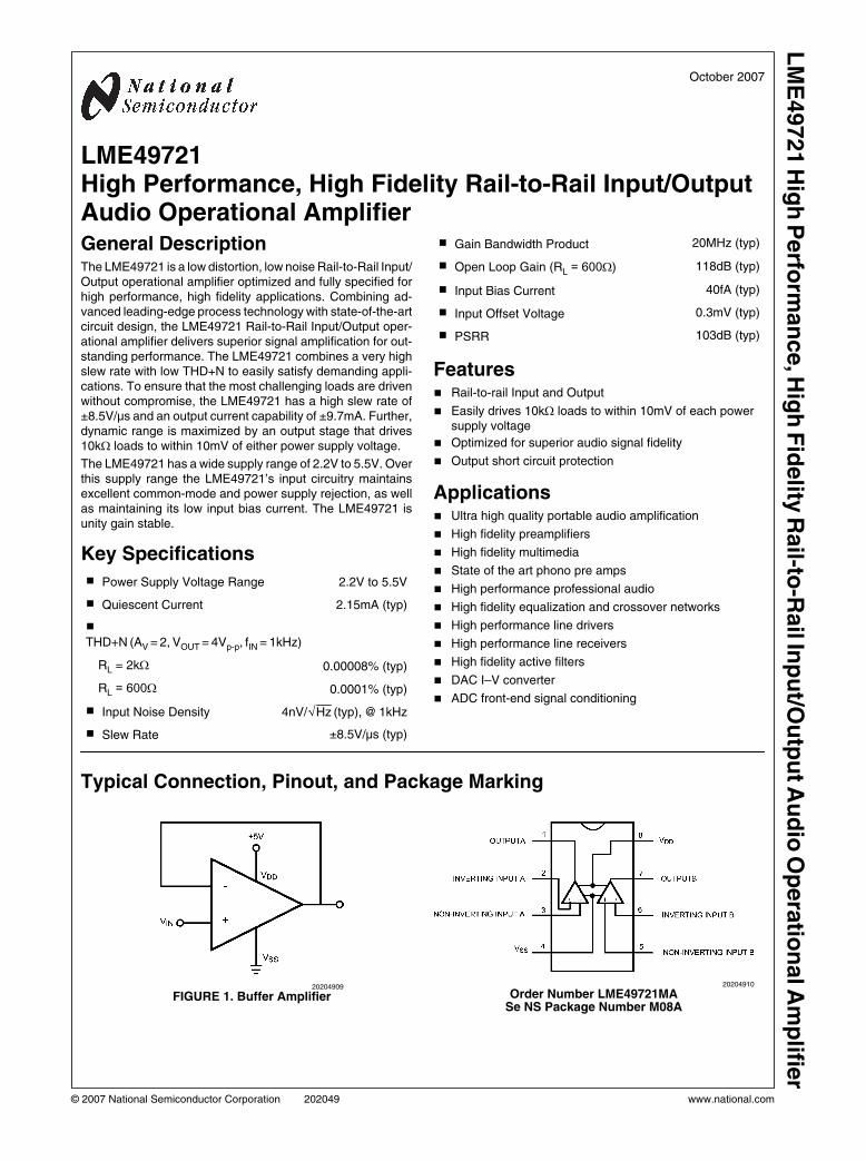
Typical Connection, Pinout, and Package Marking
20204909
FIGURE 1. Buffer Amplifier20204910
Order Number LME49721MASe NS Package Number M08A
© 2007 National Semiconductor Corporation 202049 www.national.com
LM
E49721 H
igh
Perfo
rman
ce, H
igh
Fid
elity
Rail-to
-Rail In
pu
t/Ou
tpu
t Au
dio
Op
era
tion
al A
mp
lifier
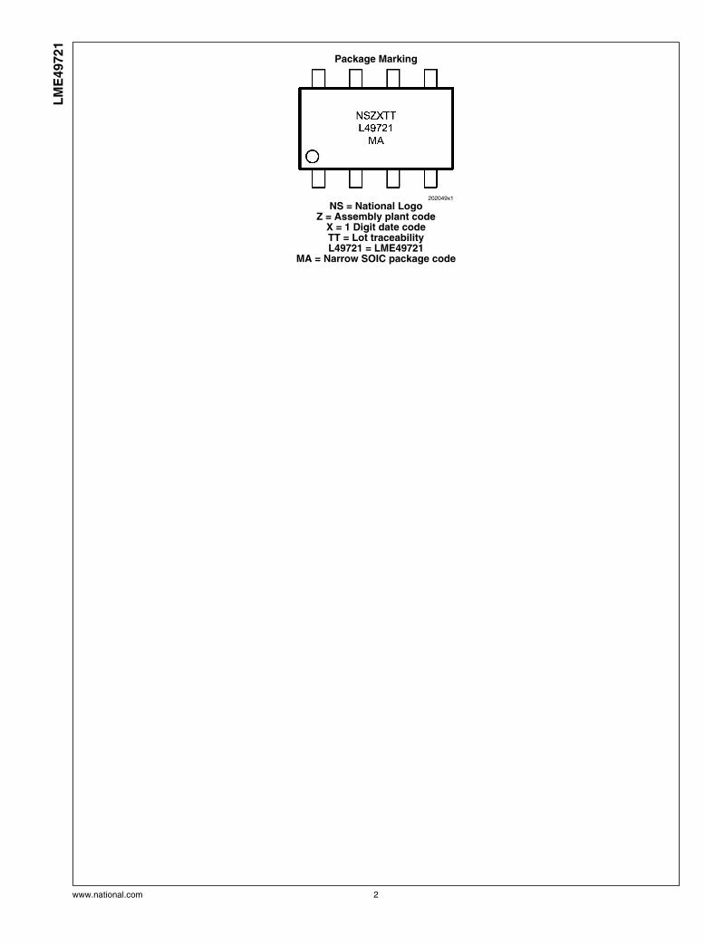
Package Marking
202049x1
NS = National LogoZ = Assembly plant code
X = 1 Digit date codeTT = Lot traceabilityL49721 = LME49721
MA = Narrow SOIC package code
www.national.com 2
LM
E49721

Absolute Maximum Ratings (Notes 1, 2)
If Military/Aerospace specified devices are required,please contact the National Semiconductor Sales Office/Distributors for availability and specifications.
Power Supply Voltage (VS = V+ - V-) 6V
Storage Temperature −65°C to 150°C
Input Voltage (V-) - 0.7V to (V+) + 0.7V
Output Short Circuit (Note 3) Continuous
Power Dissipation Internally Limited
ESD Rating (Note 4) 2000V
ESD Rating (Note 5) 200V
Junction Temperature 150°C
Thermal Resistance
θJA (SO) 165°C/W
Temperature Range
TMIN ≤ TA ≤ TMAX –40°C ≤ TA ≤ 85°C
Supply Voltage Range 2.2V ≤ VS ≤ 5.5V
Electrical Characteristics for the LME49721 The following specifications apply for the circuit shown
in Figure 1. VS = 5V, RL = 10kΩ, RSOURCE = 10Ω, fIN = 1kHz, and TA = 25°C, unless otherwise specified.
Symbol Parameter Conditions
LME49721Units
(Limits)Typical Limit
(Note 6) (Note 7)
THD+N Total Harmonic Distortion + Noise
AV = +1, VOUT = 2Vp-p,
RL = 2kΩ RL = 600Ω
0.0002
0.0002 0.001 % (max)
IMD Intermodulation DistortionAV = +1, VOUT = 2Vp-p,
Two-tone, 60Hz & 7kHz 4:10.0004 %
GBWP Gain Bandwidth Product 20 15 MHz (min)
SR Slew Rate AV = +1 8.5 V/μs (min)
FPBW Full Power Bandwidth
VOUT = 1VP-P, –3dB
referenced to output magnitude
at f = 1kHz
2.2
MHz
ts Settling timeAV = 1, 4V step
0.1% error range800 ns
en
Equivalent Input Noise Voltage fBW = 20Hz to 20kHz,
A-weighted
.707 1.13 μVP-P
(max)
Equivalent Input Noise Density f = 1kHz
A-weighted
4 6 nV/√Hz
(max)
in Current Noise Density f = 10kHz 4.0 fA/√Hz
VOS Offset Voltage 0.3 1.5 mV (max)
ΔVOS/ΔTempAverage Input Offset Voltage Drift vs
Temperature40°C ≤ TA ≤ 85°C 1.1
μV/°C
PSRRAverage Input Offset Voltage Shift vs
Power Supply Voltage 103 85 dB (min)
ISOCH-CH Channel-to-Channel Isolation fIN = 1kHz 117 dB
IB Input Bias Current VCM = VS/2 40 fA
ΔIOS/ΔTempInput Bias Current Drift vs
Temperature–40°C ≤ TA ≤ 85°C 48
fA/°C
IOS Input Offset Current VCM = VS/2 60 fA
VIN-CM
Common-Mode Input Voltage Range
(V+) – 0.1
(V-) + 0.1V (min)
CMRR Common-Mode Rejection VSS - 100mV < VCM < VDD + 100mV 93 70 dB (min)
1/f Corner Frequency 2000 Hz
AVOL Open Loop Voltage Gain
VSS - 200mV < VOUT < VDD + 200mV
RL = 600Ω 118 100 dB (min)
RL = 2kΩ 122 dB (min)
RL = 10kΩ 130 115 dB (min)
3 www.national.com
LM
E49721
Symbol Parameter Conditions
LME49721Units
(Limits)Typical Limit
(Note 6) (Note 7)
VOUTMIN Output Voltage Swing
RL = 600ΩVDD – 30mV VDD – 80mV V (min)
VSS + 30mV VSS + 80mV V (min)
RL = 10kΩ, VS = 5.0VVDD – 10mV VDD – 20mV V (min)
VSS + 10mV VSS + 20mV V (min)
IOUT Output Current RL = 250Ω, VS = 5.0V 9.7 9.3 mA (min)
IOUT-SC Short Circuit Current 100 mA
ROUT Output Impedance
fIN = 10kHz
Closed-Loop
Open-Loop
0.01
46
Ω
IS Quiescent Current per Amplifier IOUT = 0mA 2.15 3.25 mA (max)
Note 1: “Absolute Maximum Ratings” indicate limits beyond which damage to the device may occur, including inoperability and degradation of device reliabilityand/or performance. Functional operation of the device and/or non-degradation at the Absolute Maximum Ratings or other conditions beyond those indicated inthe Recommended Operating Conditions is not implied. The Recommended Operating Conditions indicate conditions at which the device is functional and thedevice should not be operated beyond such conditions. All voltages are measured with respect to the ground pin, unless otherwise specified
Note 2: The Electrical Characteristics tables list guaranteed specifications under the listed Recommended Operating Conditions except as otherwise modifiedor specified by the Electrical Characteristics Conditions and/or Notes. Typical specifications are estimations only and are not guaranteed.
Note 3: The maximum power dissipation must be derated at elevated temperatures and is dictated by TJMAX, θJA, and the ambient temperature, TA. The maximumallowable power dissipation is PDMAX = (TJMAX - TA) / θJA or the number given in Absolute Maximum Ratings, whichever is lower.
Note 4: Human body model, applicable std. JESD22-A114C.
Note 5: Machine model, applicable std. JESD22-A115-A.
Note 6: Typical values represent most likely parametric norms at TA = +25ºC, and at the Recommended Operation Conditions at the time of productcharacterization and are not guaranteed.
Note 7: Datasheet min/max specification limits are guaranteed by test or statistical analysis.
www.national.com 4
LM
E49721

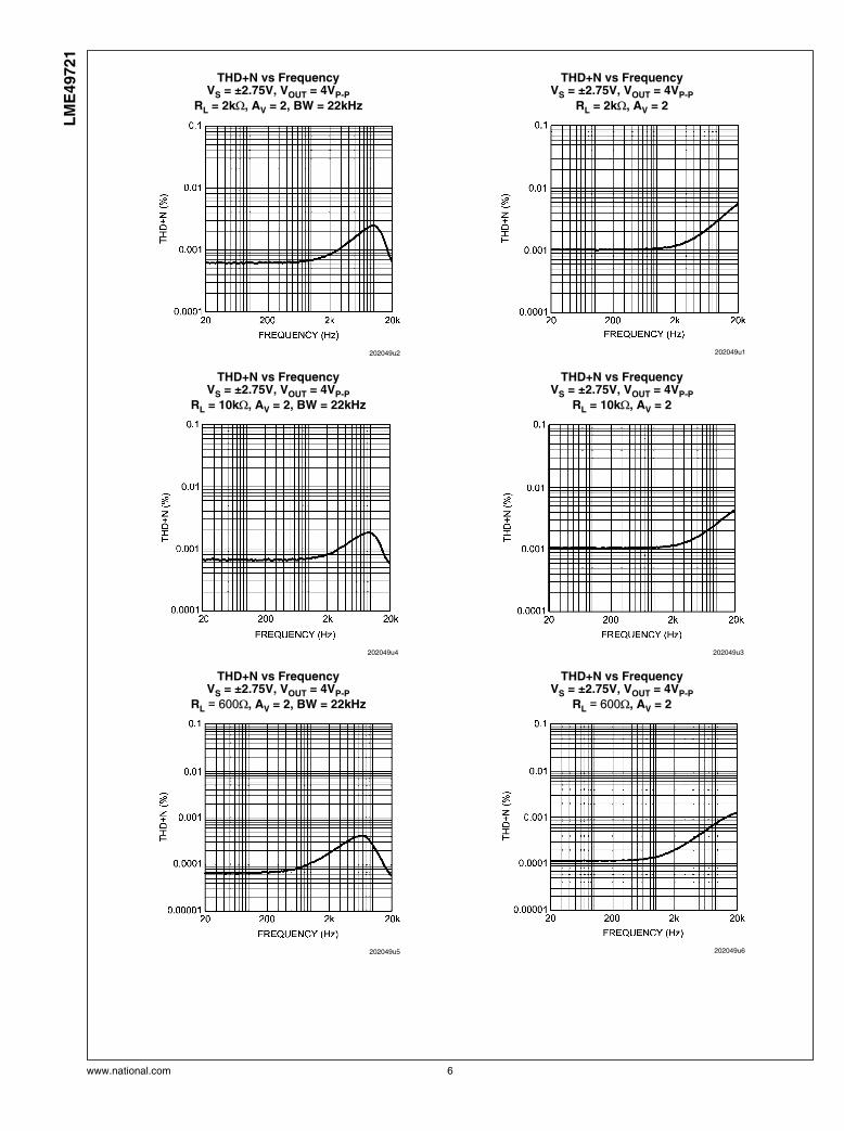
Typical Performance Characteristics Graphs were taken in dual supply configuration.
THD+N vs FrequencyVS = ±2.5V, VOUT = 4VP-P
RL = 2kΩ, AV = 2, BW = 22kHz
202049t6
THD+N vs FrequencyVS = ±2.5V, VOUT = 4VP-P
RL = 2kΩ, AV = 2
202049t5
THD+N vs FrequencyVS = ±2.5V, VOUT = 4VP-P
RL = 10kΩ, AV = 2, BW = 22kHz
202049t8
THD+N vs FrequencyVS = ±2.5V, VOUT = 4VP-P
RL = 10kΩ, AV = 2
202049t7
THD+N vs FrequencyVS = ±2.5V, VOUT = 4VP-P
RL = 600Ω, AV = 2, BW = 22kHz
202049u0
THD+N vs FrequencyVS = ±2.5V, VOUT = 4VP-P
RL = 600Ω, AV = 2
202049t9
5 www.national.com
LM
E49721
THD+N vs FrequencyVS = ±2.75V, VOUT = 4VP-P
RL = 2kΩ, AV = 2, BW = 22kHz
202049u2
THD+N vs FrequencyVS = ±2.75V, VOUT = 4VP-P
RL = 2kΩ, AV = 2
202049u1
THD+N vs FrequencyVS = ±2.75V, VOUT = 4VP-P
RL = 10kΩ, AV = 2, BW = 22kHz
202049u4
THD+N vs FrequencyVS = ±2.75V, VOUT = 4VP-P
RL = 10kΩ, AV = 2
202049u3
THD+N vs FrequencyVS = ±2.75V, VOUT = 4VP-P
RL = 600Ω, AV = 2, BW = 22kHz
202049u5
THD+N vs FrequencyVS = ±2.75V, VOUT = 4VP-P
RL = 600Ω, AV = 2
202049u6
www.national.com 6
LM
E49721
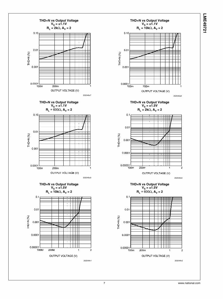
THD+N vs Output VoltageVS = ±1.1V
RL = 2kΩ, AV = 2
202049u7
THD+N vs Output VoltageVS = ±1.1V
RL = 10kΩ, AV = 2
202049u8
THD+N vs Output VoltageVS = ±1.1V
RL = 600Ω, AV = 2
202049u9
THD+N vs Output VoltageVS = ±1.5V
RL = 2kΩ, AV = 2
202049v0
THD+N vs Output VoltageVS = ±1.5V
RL = 10kΩ, AV = 2
202049v1
THD+N vs Output VoltageVS = ±1.5V
RL = 600Ω, AV = 2
202049v2
7 www.national.com
LM
E49721
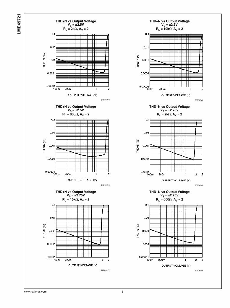
THD+N vs Output VoltageVS = ±2.5V
RL = 2kΩ, AV = 2
202049v3
THD+N vs Output VoltageVS = ±2.5V
RL = 10kΩ, AV = 2
202049v4
THD+N vs Output VoltageVS = ±2.5V
RL = 600Ω, AV = 2
202049v5
THD+N vs Output VoltageVS = ±2.75V
RL = 2kΩ, AV = 2
202049v6
THD+N vs Output VoltageVS = ±2.75V
RL = 10kΩ, AV = 2
202049v7
THD+N vs Output VoltageVS = ±2.75V
RL = 600Ω, AV = 2
202049v8
www.national.com 8
LM
E49721
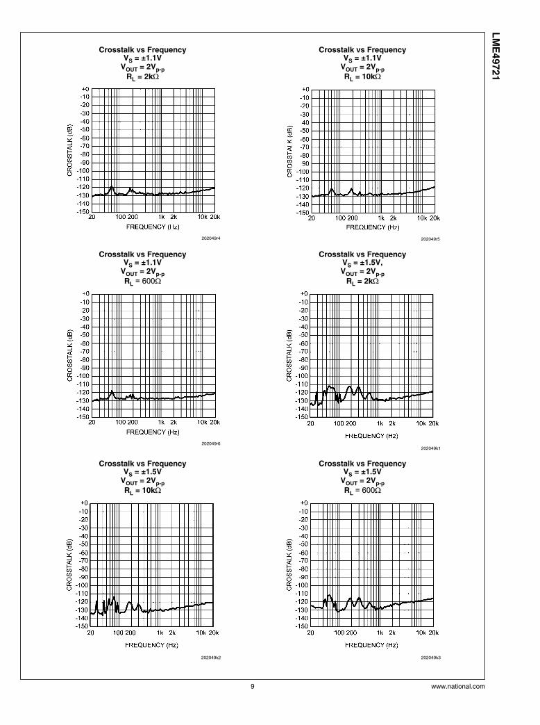
Crosstalk vs FrequencyVS = ±1.1V
VOUT = 2Vp-p
RL = 2kΩ
202049r4
Crosstalk vs FrequencyVS = ±1.1V
VOUT = 2Vp-p
RL = 10kΩ
202049r5
Crosstalk vs FrequencyVS = ±1.1V
VOUT = 2Vp-p
RL = 600Ω
202049r6
Crosstalk vs FrequencyVS = ±1.5V,VOUT = 2Vp-p
RL = 2kΩ
202049k1
Crosstalk vs FrequencyVS = ±1.5V
VOUT = 2Vp-p
RL = 10kΩ
202049k2
Crosstalk vs FrequencyVS = ±1.5V
VOUT = 2Vp-p
RL = 600Ω
202049k3
9 www.national.com
LM
E49721

Crosstalk vs FrequencyVS = ±2.5V
VOUT = 4Vp-p
RL = 2kΩ
202049k4
Crosstalk vs FrequencyVS = ±2.5V
VOUT = 4Vp-p
RL = 10kΩ
202049k5
Crosstalk vs FrequencyVS = ±2.5V
VOUT = 4Vp-p
RL = 600Ω
202049k6
Crosstalk vs FrequencyVS = ±2.75VVOUT = 4Vp-p
RL = 2kΩ
202049k7
Crosstalk vs FrequencyVS = ±2.75VVOUT = 4Vp-p
RL = 10kΩ
202049k8
Crosstalk vs FrequencyVS = ±2.75VVOUT = 4Vp-p
RL = 600Ω
202049k9
www.national.com 10
LM
E49721
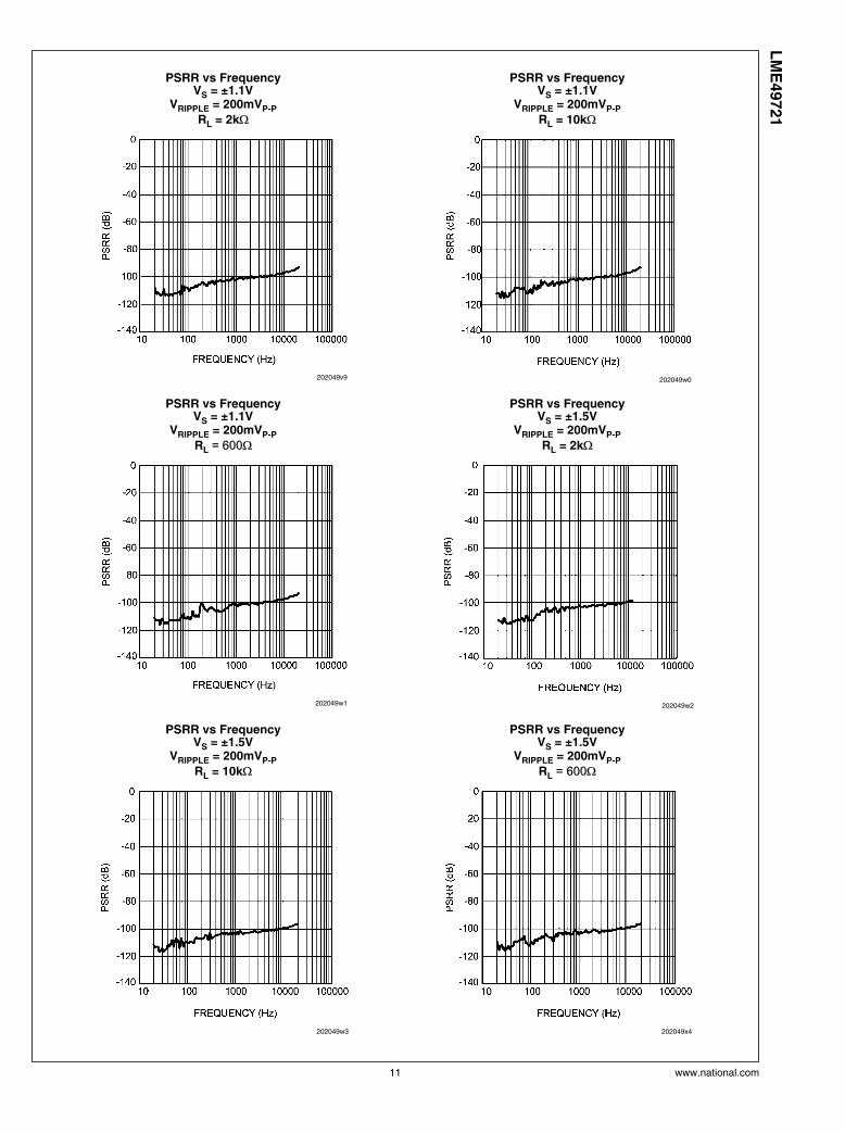
PSRR vs FrequencyVS = ±1.1V
VRIPPLE = 200mVP-P
RL = 2kΩ
202049v9
PSRR vs FrequencyVS = ±1.1V
VRIPPLE = 200mVP-P
RL = 10kΩ
202049w0
PSRR vs FrequencyVS = ±1.1V
VRIPPLE = 200mVP-P
RL = 600Ω
202049w1
PSRR vs FrequencyVS = ±1.5V
VRIPPLE = 200mVP-P
RL = 2kΩ
202049w2
PSRR vs FrequencyVS = ±1.5V
VRIPPLE = 200mVP-P
RL = 10kΩ
202049w3
PSRR vs FrequencyVS = ±1.5V
VRIPPLE = 200mVP-P
RL = 600Ω
202049x4
11 www.national.com
LM
E49721
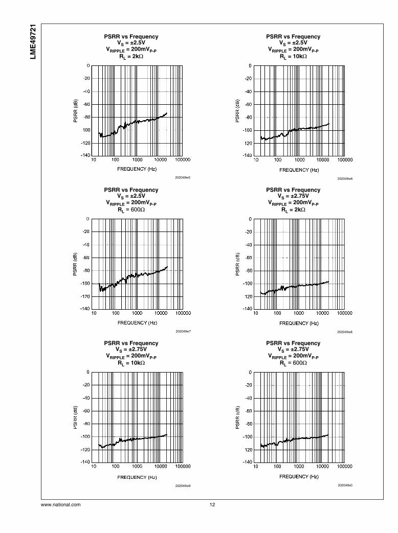
PSRR vs FrequencyVS = ±2.5V
VRIPPLE = 200mVP-P
RL = 2kΩ
202049w5
PSRR vs FrequencyVS = ±2.5V
VRIPPLE = 200mVP-P
RL = 10kΩ
202049w6
PSRR vs FrequencyVS = ±2.5V
VRIPPLE = 200mVP-P
RL = 600Ω
202049w7
PSRR vs FrequencyVS = ±2.75V
VRIPPLE = 200mVP-P
RL = 2kΩ
202049w8
PSRR vs FrequencyVS = ±2.75V
VRIPPLE = 200mVP-P
RL = 10kΩ
202049w9
PSRR vs FrequencyVS = ±2.75V
VRIPPLE = 200mVP-P
RL = 600Ω
202049x0
www.national.com 12
LM
E49721
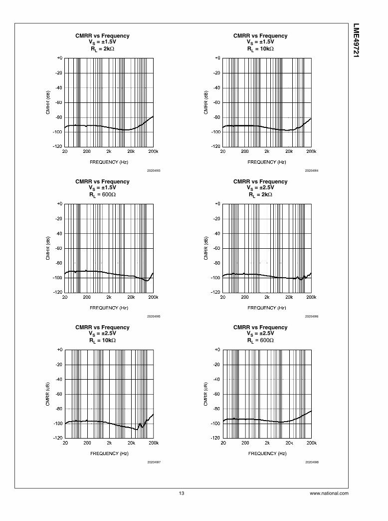
CMRR vs FrequencyVS = ±1.5V
RL = 2kΩ
202049l3
CMRR vs FrequencyVS = ±1.5V
RL = 10kΩ
202049l4
CMRR vs FrequencyVS = ±1.5V
RL = 600Ω
202049l5
CMRR vs FrequencyVS = ±2.5V
RL = 2kΩ
202049l6
CMRR vs FrequencyVS = ±2.5V
RL = 10kΩ
202049l7
CMRR vs FrequencyVS = ±2.5V
RL = 600Ω
202049l8
13 www.national.com
LM
E49721
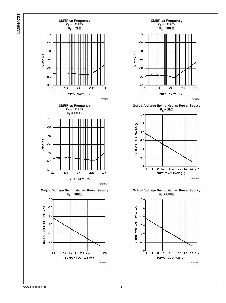
CMRR vs FrequencyVS = ±2.75V
RL = 2kΩ
202049l9
CMRR vs FrequencyVS = ±2.75V
RL = 10kΩ
202049m0
CMRR vs FrequencyVS = ±2.75V
RL = 600Ω
202049m1
Output Voltage Swing Neg vs Power SupplyRL = 2kΩ
202049s9
Output Voltage Swing Neg vs Power SupplyRL = 10kΩ
202049t0
Output Voltage Swing Neg vs Power SupplyRL = 600Ω
202049t1
www.national.com 14
LM
E49721
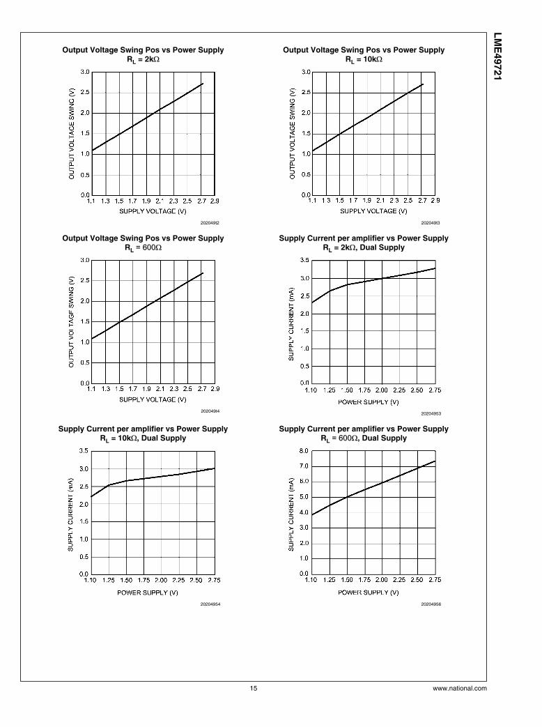
Output Voltage Swing Pos vs Power SupplyRL = 2kΩ
202049t2
Output Voltage Swing Pos vs Power SupplyRL = 10kΩ
202049t3
Output Voltage Swing Pos vs Power SupplyRL = 600Ω
202049t4
Supply Current per amplifier vs Power SupplyRL = 2kΩ, Dual Supply
20204953
Supply Current per amplifier vs Power SupplyRL = 10kΩ, Dual Supply
20204954
Supply Current per amplifier vs Power SupplyRL = 600Ω, Dual Supply
20204956
15 www.national.com
LM
E49721

Application Information
DISTORTION MEASUREMENTS
The vanishingly low residual distortion produced byLME49721 is below the capabilities of all commercially avail-able equipment. This makes distortion measurements justslightly more difficult than simply connecting a distortion me-ter to the amplifier's inputs and outputs. The solution. howev-er, is quite simple: an additional resistor. Adding this resistorextends the resolution of the distortion measurement equip-ment.
The LME49721's low residual is an input referred internal er-ror. As shown in Figure 1, adding the 10Ω resistor connectedbetween athe amplifier's inverting and non-inverting inputs
changes the amplifier's noise gain. The result is that the errorsignal (distortion) is amplified by a factor of 101. Although theamplifier's closed-loop gain is unaltered, the feedback avail-able to correct distortion errors is reduced by 101. To ensureminimum effects on distortion measurements, keep the valueof R1 low as shown in Figure 1.
This technique is verified by duplicating the measurementswith high closed loop gain and/or making the measurementsat high frequencies. Doing so, produces distortion compo-nents that are within equipments capabilities. Thisdatasheet's THD+N and IMD values were generated usingthe above described circuit connected to an Audio PrecisionSystem Two Cascade.
202049x2
FIGURE 1. THD+N and IMD Distortion Test Circuit with AV = 2
OPERATING RATINGS AND BASIC DESIGN GUIDELINES
The LME49721 has a supply voltage range from +2.2V to+5.5V single supply or ±1.1 to ±2.75V dual supply.
Bypassed capacitors for the supplies should be placed asclose to the amplifier as possible. This will help minimize anyinductance between the power supply and the supply pins. Inaddition to a 10μF capacitor, a 0.1μF capacitor is also rec-ommended in CMOS amplifiers.
The amplifier's inputs lead lengths should also be as short aspossible. If the op amp does not have a bypass capacitor, itmay oscillate.
BASIC AMPLIFIER CONFIGURATIONS
The LME49721 may be operated with either a single supplyor dual supplies. Figure 2 shows the typical connection for asingle supply inverting amplifier. The output voltage for a sin-gle supply amplifier will be centered around the common-mode voltage Vcm. Note, the voltage applied to the Vcminsures the output stays above ground. Typically, the Vcm
should be equal to VDD/2. This is done by putting a resistordivider ckt at this node, see Figure 2.
202049n3
FIGURE 2. Single Supply Inverting Op Amp
www.national.com 16
LM
E49721
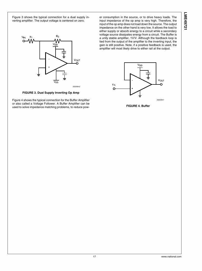
Figure 3 shows the typical connection for a dual supply in-verting amplifier. The output voltage is centered on zero.
202049n2
FIGURE 3. Dual Supply Inverting Op Amp
Figure 4 shows the typical connection for the Buffer Amplifieror also called a Voltage Follower. A Buffer Amplifier can beused to solve impedance matching problems, to reduce pow-
er consumption in the source, or to drive heavy loads. Theinput impedance of the op amp is very high. Therefore, theinput of the op amp does not load down the source. The outputimpedance on the other hand is very low. It allows the load toeither supply or absorb energy to a circuit while a secondaryvoltage source dissipates energy from a circuit. The Buffer isa unity stable amplifier, 1V/V. Although the feedback loop istied from the output of the amplifier to the inverting input, thegain is still positive. Note, if a positive feedback is used, theamplifier will most likely drive to either rail at the output.
202049n1
FIGURE 4. Buffer
17 www.national.com
LM
E49721
Typical Applications
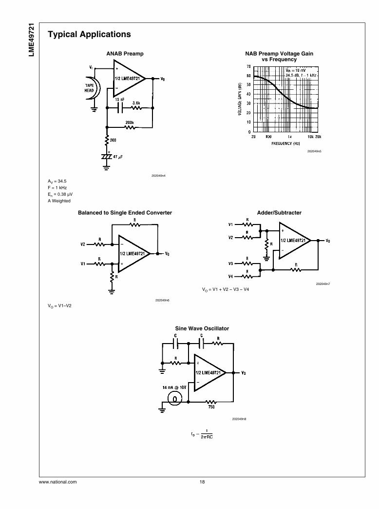
ANAB Preamp
202049n4
AV = 34.5
F = 1 kHz
En = 0.38 μV
A Weighted
NAB Preamp Voltage Gainvs Frequency
202049n5
Balanced to Single Ended Converter
202049n6
VO = V1–V2
Adder/Subtracter
202049n7
VO = V1 + V2 − V3 − V4
Sine Wave Oscillator
202049n8
www.national.com 18
LM
E49721

Second Order High Pass Filter(Butterworth)
202049n9
Illustration is f0 = 1 kHz
Second Order Low Pass Filter(Butterworth)
202049o0
Illustration is f0 = 1 kHz
State Variable Filter
202049o1
Illustration is f0 = 1 kHz, Q = 10, ABP = 1
19 www.national.com
LM
E49721
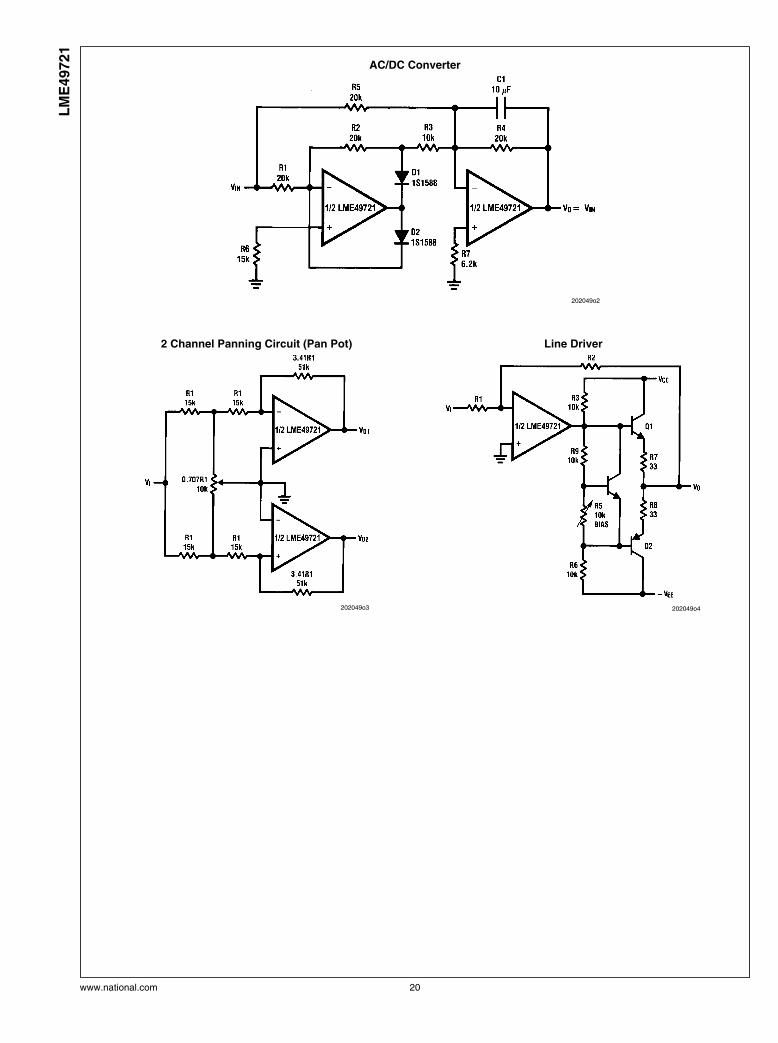
AC/DC Converter
202049o2
2 Channel Panning Circuit (Pan Pot)
202049o3
Line Driver
202049o4
www.national.com 20
LM
E49721

Tone Control
202049o5
Illustration is:
fL = 32 Hz, fLB = 320 Hz
fH =11 kHz, fHB = 1.1 kHz
202049o6
RIAA Preamp
202049o8
Av = 35 dB
En = 0.33 μV
S/N = 90 dB
f = 1 kHz
A Weighted
A Weighted, VIN = 10 mV
@f = 1 kHz
21 www.national.com
LM
E49721

Balanced Input Mic Amp
202049o7
Illustration is:
V0 = 101(V2 − V1)
www.national.com 22
LM
E49721
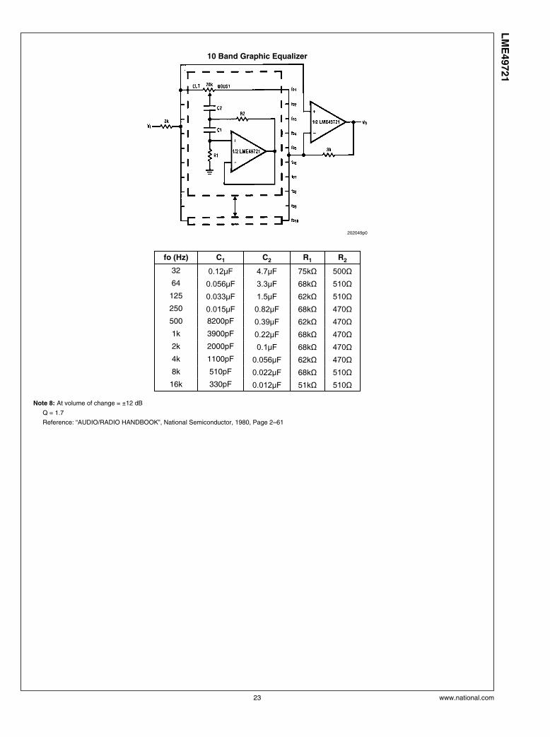
10 Band Graphic Equalizer
202049p0
fo (Hz) C1 C2 R1 R2
32 0.12μF 4.7μF 75kΩ 500Ω64 0.056μF 3.3μF 68kΩ 510Ω
125 0.033μF 1.5μF 62kΩ 510Ω250 0.015μF 0.82μF 68kΩ 470Ω500 8200pF 0.39μF 62kΩ 470Ω1k 3900pF 0.22μF 68kΩ 470Ω2k 2000pF 0.1μF 68kΩ 470Ω4k 1100pF 0.056μF 62kΩ 470Ω8k 510pF 0.022μF 68kΩ 510Ω
16k 330pF 0.012μF 51kΩ 510Ω
Note 8: At volume of change = ±12 dB
Q = 1.7
Reference: “AUDIO/RADIO HANDBOOK”, National Semiconductor, 1980, Page 2–61
23 www.national.com
LM
E49721
Revision History
Rev Date Description
1.0 09/26/07 Initial release.
1.1 10/01/07 Input more info under the Buffer Amplifier.
www.national.com 24
LM
E49721
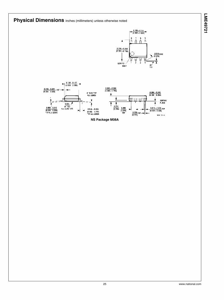
Physical Dimensions inches (millimeters) unless otherwise noted
NS Package M08A
25 www.national.com
LM
E49721
NotesL
ME
49721 H
igh
Perf
orm
an
ce, H
igh
Fid
elity
Rail-t
o-R
ail In
pu
t/O
utp
ut A
ud
io O
pera
tio
nal A
mp
lifi
er
THE CONTENTS OF THIS DOCUMENT ARE PROVIDED IN CONNECTION WITH NATIONAL SEMICONDUCTOR CORPORATION(“NATIONAL”) PRODUCTS. NATIONAL MAKES NO REPRESENTATIONS OR WARRANTIES WITH RESPECT TO THE ACCURACYOR COMPLETENESS OF THE CONTENTS OF THIS PUBLICATION AND RESERVES THE RIGHT TO MAKE CHANGES TOSPECIFICATIONS AND PRODUCT DESCRIPTIONS AT ANY TIME WITHOUT NOTICE. NO LICENSE, WHETHER EXPRESS,IMPLIED, ARISING BY ESTOPPEL OR OTHERWISE, TO ANY INTELLECTUAL PROPERTY RIGHTS IS GRANTED BY THISDOCUMENT.
TESTING AND OTHER QUALITY CONTROLS ARE USED TO THE EXTENT NATIONAL DEEMS NECESSARY TO SUPPORTNATIONAL’S PRODUCT WARRANTY. EXCEPT WHERE MANDATED BY GOVERNMENT REQUIREMENTS, TESTING OF ALLPARAMETERS OF EACH PRODUCT IS NOT NECESSARILY PERFORMED. NATIONAL ASSUMES NO LIABILITY FORAPPLICATIONS ASSISTANCE OR BUYER PRODUCT DESIGN. BUYERS ARE RESPONSIBLE FOR THEIR PRODUCTS ANDAPPLICATIONS USING NATIONAL COMPONENTS. PRIOR TO USING OR DISTRIBUTING ANY PRODUCTS THAT INCLUDENATIONAL COMPONENTS, BUYERS SHOULD PROVIDE ADEQUATE DESIGN, TESTING AND OPERATING SAFEGUARDS.
EXCEPT AS PROVIDED IN NATIONAL’S TERMS AND CONDITIONS OF SALE FOR SUCH PRODUCTS, NATIONAL ASSUMES NOLIABILITY WHATSOEVER, AND NATIONAL DISCLAIMS ANY EXPRESS OR IMPLIED WARRANTY RELATING TO THE SALEAND/OR USE OF NATIONAL PRODUCTS INCLUDING LIABILITY OR WARRANTIES RELATING TO FITNESS FOR A PARTICULARPURPOSE, MERCHANTABILITY, OR INFRINGEMENT OF ANY PATENT, COPYRIGHT OR OTHER INTELLECTUAL PROPERTYRIGHT.
LIFE SUPPORT POLICY
NATIONAL’S PRODUCTS ARE NOT AUTHORIZED FOR USE AS CRITICAL COMPONENTS IN LIFE SUPPORT DEVICES ORSYSTEMS WITHOUT THE EXPRESS PRIOR WRITTEN APPROVAL OF THE CHIEF EXECUTIVE OFFICER AND GENERALCOUNSEL OF NATIONAL SEMICONDUCTOR CORPORATION. As used herein:
Life support devices or systems are devices which (a) are intended for surgical implant into the body, or (b) support or sustain life andwhose failure to perform when properly used in accordance with instructions for use provided in the labeling can be reasonably expectedto result in a significant injury to the user. A critical component is any component in a life support device or system whose failure to performcan be reasonably expected to cause the failure of the life support device or system or to affect its safety or effectiveness.
National Semiconductor and the National Semiconductor logo are registered trademarks of National Semiconductor Corporation. All otherbrand or product names may be trademarks or registered trademarks of their respective holders.
Copyright© 2007 National Semiconductor Corporation
For the most current product information visit us at www.national.com
National SemiconductorAmericas CustomerSupport CenterEmail:[email protected]: 1-800-272-9959
National Semiconductor EuropeCustomer Support CenterFax: +49 (0) 180-530-85-86Email: [email protected] Tel: +49 (0) 69 9508 6208English Tel: +49 (0) 870 24 0 2171Français Tel: +33 (0) 1 41 91 8790
National Semiconductor AsiaPacific Customer Support CenterEmail: [email protected]
National Semiconductor JapanCustomer Support CenterFax: 81-3-5639-7507Email: [email protected]: 81-3-5639-7560
www.national.com