lmp90100 and lmp9009x sensor afe system: … · lmp90100 ib1 micro-controller sclk vin0 vin2 vin4...
TRANSCRIPT
LMP90100
IB1
Micro-Controller
SCLK
VIN0
VIN2
VIN4
VIN6/VREFP2
4-W
ire R
TD
3-W
ire R
TD
2 -W
ire R
TD
1
4
2
3
...
...
VIN7/ VREFN2
CSB
SDO/DRDYB
SDI
D0
D6/DRDYB
...
XOUTCLK/XINGND
VA
IB2
VREFN1
...
VIOVA
LEDs/Switches
VREFP1
The
rmoc
oupl
e
+
-
Product Channel Configuration Current Sources
LMP90100 4 Differential/7 Single-Ended Yes
LMP90099 4 Differential/7 Single-Ended No
LMP90098 2 Differential/4 Single-Ended Yes
LMP90097 2 Differential/4 Single-Ended No
LM90xxx 24-bit Sensor AFE Family of Products
Product
Folder
Sample &Buy
Technical
Documents
Tools &
Software
Support &Community
An IMPORTANT NOTICE at the end of this data sheet addresses availability, warranty, changes, use in safety-critical applications,intellectual property matters and other important disclaimers. PRODUCTION DATA.
LMP90100, LMP90099, LMP90098, LMP90097SNAS510S –JANUARY 2011–REVISED JANUARY 2016
LMP90100 and LMP9009x Sensor AFE System: Multichannel, Low-Power, 24-Bit SensorAFE With True Continuous Background Calibration
1 Features
1
1
• 24-Bit, Low-Power Sigma-Delta ADC• True Continuous Background Calibration at all
Gains• In-Place System Calibration Using Expected
Value Programming• Low-Noise Programmable Gain (1x to 128x)• Continuous Background Open / Short and Out-of-
Range Sensor Diagnostics• 8 Output Data Rates (ODR) With Single-Cycle
Settling• 2 Matched Excitation Current Sources From 100
µA to 1000 µA (LMP90100/LMP90098)• 4-DIFF / 7-SE Inputs (LMP90100/LMP90099)• 2-DIFF / 4-SE Inputs (LMP90098/LMP90097)• 7 General-Purpose Input/Output Pins• Chopper-Stabilized Buffer for Low Offset• SPI 4/3-wire With CRC Data Link Error Detection• 50-Hz to 60-Hz Line Rejection at ODR
≤13.42 SPS• Independent Gain and ODR Selection per
Channel• Supported by WEBENCH® Sensor AFE Designer• Automatic Channel Sequencer• Key Specifications
– ENOB/NFR Up to 21.5/19 Bits– Offset Error (Typical) 8.4 nV– Gain Error (Typical) 7 ppm– Total Noise < 10 µV-rms– Integral Nonlinearity (INL Maximum) ± 15 ppm
of FSR– Output Data Rates (ODR) 1.6775 - 214.65
SPS
– Analog Voltage, VA 2.85 to 5.5 V– Operating Temp Range –40°C to 125°C– 28-Pin HTSSOP Exposed Pad
2 Applications• Temperature and Pressure Transmitters• Strain Gauge Interface• Industrial Process Control
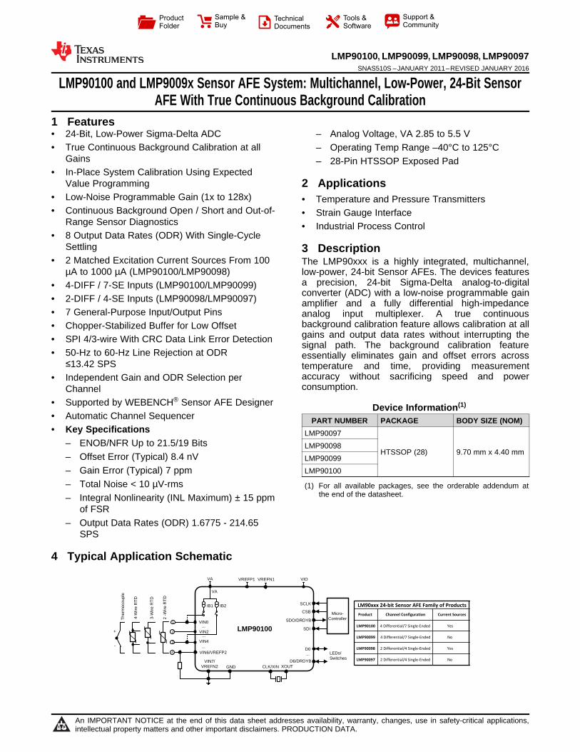
3 DescriptionThe LMP90xxx is a highly integrated, multichannel,low-power, 24-bit Sensor AFEs. The devices featuresa precision, 24-bit Sigma-Delta analog-to-digitalconverter (ADC) with a low-noise programmable gainamplifier and a fully differential high-impedanceanalog input multiplexer. A true continuousbackground calibration feature allows calibration at allgains and output data rates without interrupting thesignal path. The background calibration featureessentially eliminates gain and offset errors acrosstemperature and time, providing measurementaccuracy without sacrificing speed and powerconsumption.
Device Information(1)
PART NUMBER PACKAGE BODY SIZE (NOM)LMP90097
HTSSOP (28) 9.70 mm x 4.40 mmLMP90098LMP90099LMP90100
(1) For all available packages, see the orderable addendum atthe end of the datasheet.
4 Typical Application Schematic

2
LMP90100, LMP90099, LMP90098, LMP90097SNAS510S –JANUARY 2011–REVISED JANUARY 2016 www.ti.com
Product Folder Links: LMP90100 LMP90099 LMP90098 LMP90097
Submit Documentation Feedback Copyright © 2011–2016, Texas Instruments Incorporated
Table of Contents1 Features .................................................................. 12 Applications ........................................................... 13 Description ............................................................. 14 Typical Application Schematic ............................. 15 Revision History..................................................... 26 Description (continued)......................................... 37 Pin Configuration and Functions ......................... 48 Specifications......................................................... 5
8.1 Absolute Maximum Ratings ...................................... 58.2 ESD Ratings.............................................................. 58.3 Recommended Operating Conditions....................... 58.4 Thermal Information .................................................. 58.5 Electrical Characteristics .......................................... 68.6 SPI Timing Requirements ....................................... 118.7 CBS Setup and Hold Timing Requirements ........... 118.8 SCLK and SDI Timing Requirements ..................... 128.9 SDO Timing Requirements ..................................... 128.10 SDO and DRDYB Timing Requirements .............. 138.11 Typical Characteristics .......................................... 14
9 Detailed Description ............................................ 209.1 Overview ................................................................. 209.2 Functional Block Diagram ....................................... 20
9.3 Feature Description................................................. 209.4 Device Functional Modes........................................ 329.5 Programming........................................................... 339.6 Register Maps ......................................................... 45
10 Application and Implementation........................ 5610.1 Application Information.......................................... 5610.2 Typical Applications .............................................. 57
11 Power Supply Recommendations ..................... 6311.1 VA and VIO ........................................................... 6311.2 VREF..................................................................... 63
12 Layout................................................................... 6412.1 Layout Guidelines ................................................. 6412.2 Layout Example .................................................... 64
13 Device and Documentation Support ................. 6513.1 Device Support .................................................... 6513.2 Related Links ........................................................ 6613.3 Community Resources.......................................... 6613.4 Trademarks ........................................................... 6613.5 Electrostatic Discharge Caution............................ 6613.6 Glossary ................................................................ 66
14 Mechanical, Packaging, and OrderableInformation ........................................................... 66
5 Revision HistoryNOTE: Page numbers for previous revisions may differ from page numbers in the current version.
Changes from Revision R (January 2015) to Revision S Page
• Changed Buffer Enable/Disable. ......................................................................................................................................... 54• Changed BUF_EN = 1 to 0. ................................................................................................................................................ 56
Changes from Revision Q (December 2014) to Revision R Page
• Added SDO Timing Requirements back in. ......................................................................................................................... 12
Changes from Revision P (March 2013) to Revision Q Page
• Added Pin Configuration and Functions section, ESD Ratings table, Feature Description section, Device FunctionalModes, Application and Implementation section, Power Supply Recommendations section, Layout section, Deviceand Documentation Support section, and Mechanical, Packaging, and Orderable Information section .............................. 1
• Added footnote to INL, GE, and Crosstalk specifications. ..................................................................................................... 6• Changed tDOD1 specification to 27ns..................................................................................................................................... 12• Added sentence to the end of the Reset and Restart section.............................................................................................. 32• Deleted CH_STS from Compute the CRC... sentence......................................................................................................... 40
Changes from Revision O (March 2013) to Revision P Page
• Changed layout of National Data Sheet to TI format ........................................................................................................... 48
3
LMP90100, LMP90099, LMP90098, LMP90097www.ti.com SNAS510S –JANUARY 2011–REVISED JANUARY 2016
Product Folder Links: LMP90100 LMP90099 LMP90098 LMP90097
Submit Documentation FeedbackCopyright © 2011–2016, Texas Instruments Incorporated
6 Description (continued)Another feature of the LMP90100/LMP90099/LMP90098/LMP90097 is continuous background sensordiagnostics, allowing the detection of open and short-circuit conditions and out-of-range signals, without requiringuser intervention, resulting in enhanced system reliability.
Two sets of independent external reference voltage pins allow multiple ratiometric measurements. In addition,two matched programmable current sources are available in the LMP90100/LMP90098 to excite external sensorssuch as resistive temperature detectors and bridge sensors. Furthermore, seven GPIO pins are provided forinterfacing to external LEDs and switches to simplify control across an isolation barrier.
Collectively, these features make the LMP90100/LMP90099/LMP90098/LMP90097 complete analog front-endsfor low-power, precision sensor applications such as temperature, pressure, strain gauge, and industrial processcontrol. The LMP90100/LMP90099/LMP90098/LMP90097 are ensured over the extended temperature range of-40°C to +125°C and are available in a 28-pin HTSSOP package with an exposed pad.

1VA
2VIN0
3VIN1
4VIN2
5VIN3
6VIN4
7VIN5
8VREFP1
9VREFN1
10VIN6/VREFP2
11
12
28
27
26
25
24
23
22
21
20
19
18
17
VIO
D6/DRDYB
D5
D4
D3
D2
D1
D0
SDO/DRDYB
SDI
SCLK
13
14
LMP90xxx28-pin HTSSOP
16
15
VIN7/VREFN2
IB2
IB1
XOUT
CSB
GND
XIN/CLK
LMP90100/LMP90098 only
LMP90100/LMP90099 only
4
LMP90100, LMP90099, LMP90098, LMP90097SNAS510S –JANUARY 2011–REVISED JANUARY 2016 www.ti.com
Product Folder Links: LMP90100 LMP90099 LMP90098 LMP90097
Submit Documentation Feedback Copyright © 2011–2016, Texas Instruments Incorporated
7 Pin Configuration and Functions
HTSSOP (PWP0028A) PACKAGE28 PINS
TOP VIEW
See below for specific information regarding options LMP90099, LMP90098, and LMP90097.
Pin FunctionsPIN
TYPE DESCRIPTIONNAME NO.
VA 1 Analog Supply Analog power supply pinVIN0 to VIN2 2 to 4 Analog Input Analog input pins
VIN3 to VIN55 to 7
(LMP90100, LMP90099only)
Analog Input Analog input pins
VIN3 to VIN55 - 7
(LMP90098, LMP90097only)
No Connect No connect: must be left unconnected
VREFP1 8 Analog Input Positive reference inputVREFN1 9 Analog Input Negative reference inputVIN6 / VREFP2 10 Analog Input Analog input pin or VREFP2 inputVIN7 / VREFN2 11 Analog Input Analog input pin or VREFN2 input
IB2, IB112 to 13
(LMP90100, LMP90098only)
Analog Output Excitation current sources for external RTDs
IB2, IB112 - 13
(LMP90099, LMP90097only)
No Connect No connect: must be left unconnected
XOUT 14 Analog Output External crystal oscillator connectionXIN / CLK 15 Analog Input External crystal oscillator connection or external clock inputGND 16 Ground Power supply groundCSB 17 Digital Input Chip select barSCLK 18 Digital Input Serial clockSDI 19 Digital Input Serial data inputSDO / DRDYB 20 Digital Output Serial data output and data ready barD0 to D5 21 to 26 Digital IO General purpose input/output (GPIO) pinsD6 / DRDYB 27 Digital IO General purpose input/output pin or data ready barVIO 28 Digital Supply Digital input/output supply pinThermal Pad — — You can leave this thermal pad floating.

5
LMP90100, LMP90099, LMP90098, LMP90097www.ti.com SNAS510S –JANUARY 2011–REVISED JANUARY 2016
Product Folder Links: LMP90100 LMP90099 LMP90098 LMP90097
Submit Documentation FeedbackCopyright © 2011–2016, Texas Instruments Incorporated
(1) All voltages are measured with respect to GND, unless otherwise specified(2) Absolute Maximum Ratings indicate limits beyond which damage to the device may occur. Recommended Operating Conditions indicate
conditions for which the device is functional, but do not ensure specific performance limits. For ensured specifications and testconditions, see the Electrical Characteristics . The ensured specifications apply only for the test conditions listed. Some performancecharacteristics may degrade when the device is not operated under the listed test conditions.
(3) For soldering specifications: see product folder at www.ti.com and SNOA549.(4) When the input voltage (VIN) exceeds the power supply (VIN < GND or VIN > VA), the current at that pin must be limited to 5mA and
VIN has to be within the Absolute Maximum Rating for that pin. The 20 mA package input current rating limits the number of pins thatcan safely exceed the power supplies with current flow to four pins.
8 Specifications
8.1 Absolute Maximum RatingsSee (1) (2) (3).
MIN MAX UNITVA Analog Supply Voltage -0.3 6.0 VVIO Digital I/O Supply Voltage -0.3 6.0 VVREF Reference Voltage -0.3 VA+0.3 V
Voltage on Any Analog Input Pin to GND (4) -0.3 VA+0.3 VVoltage on Any Digital Input PIN to GND (4) -0.3 VIO+0.3 VVoltage on SDO (4) -0.3 VIO+0.3 VInput Current at Any Pin (4) 5 mAOutput Current Source or Sink by SDO 3 mATotal Package Input and Output Current 20 mA
TJMAX Junction Temperature 150 °CTstg Storage Temperature –65 150 °C
(1) JEDEC document JEP155 states that 500-V HBM allows safe manufacturing with a standard ESD control process.(2) JEDEC document JEP157 states that 250-V CDM allows safe manufacturing with a standard ESD control process.
8.2 ESD RatingsVALUE UNIT
V(ESD) Electrostatic discharge
Human-body model (HBM), per ANSI/ESDA/JEDEC JS-001 (1) ±2500
VCharged-device model (CDM), per JEDEC specification JESD22-C101 (2)
±1250
Machine Model (MM) +200
8.3 Recommended Operating ConditionsMIN MAX UNIT
VA Analog Supply Voltage 2.85 5.5 VVIO Digital I/O Supply Voltage 2.7 5.5 VVIN Full Scale Input Range ±VREF / PGA VVREF Reference Voltage 0.5 VA V
Temperature Range for Electrical Characteristics TMIN = –40 TMAX = 125 °CTA Operating Temperature Range –40 125 °C
(1) For more information about traditional and new thermal metrics, see the IC Package Thermal Metrics application report, SPRA953.(2) The maximum power dissipation is a function of TJ(MAX) AND θJA. The maximum allowable power dissipation at any ambient
temperature is PD = (TJ(MAX) - TA) / θJA.
8.4 Thermal Information
THERMAL METRIC (1)
LMP90100,LMP9009x
UNITPWP28 PINS
RθJA Junction-to-ambient thermal resistance (2) 41 °C/W
6
LMP90100, LMP90099, LMP90098, LMP90097SNAS510S –JANUARY 2011–REVISED JANUARY 2016 www.ti.com
Product Folder Links: LMP90100 LMP90099 LMP90098 LMP90097
Submit Documentation Feedback Copyright © 2011–2016, Texas Instruments Incorporated
(1) This parameter is specified by design and/or characterization and is not tested in production
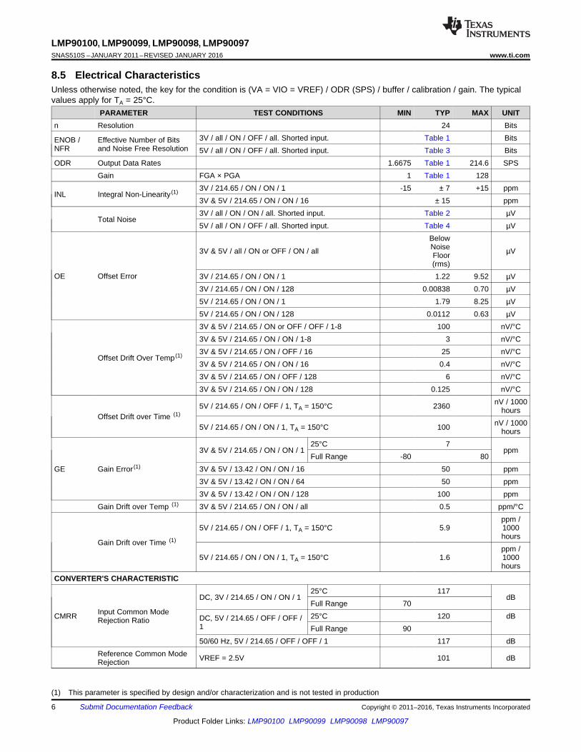
8.5 Electrical CharacteristicsUnless otherwise noted, the key for the condition is (VA = VIO = VREF) / ODR (SPS) / buffer / calibration / gain. The typicalvalues apply for TA = 25°C.
PARAMETER TEST CONDITIONS MIN TYP MAX UNITn Resolution 24 Bits
ENOB /NFR
Effective Number of Bitsand Noise Free Resolution
3V / all / ON / OFF / all. Shorted input. Table 1 Bits5V / all / ON / OFF / all. Shorted input. Table 3 Bits
ODR Output Data Rates 1.6675 Table 1 214.6 SPSGain FGA × PGA 1 Table 1 128
INL Integral Non-Linearity (1) 3V / 214.65 / ON / ON / 1 -15 ± 7 +15 ppm3V & 5V / 214.65 / ON / ON / 16 ± 15 ppm
Total Noise3V / all / ON / ON / all. Shorted input. Table 2 µV5V / all / ON / OFF / all. Shorted input. Table 4 µV
OE Offset Error
3V & 5V / all / ON or OFF / ON / all
BelowNoiseFloor(rms)
µV
3V / 214.65 / ON / ON / 1 1.22 9.52 µV3V / 214.65 / ON / ON / 128 0.00838 0.70 µV5V / 214.65 / ON / ON / 1 1.79 8.25 µV5V / 214.65 / ON / ON / 128 0.0112 0.63 µV
Offset Drift Over Temp (1)
3V & 5V / 214.65 / ON or OFF / OFF / 1-8 100 nV/°C3V & 5V / 214.65 / ON / ON / 1-8 3 nV/°C3V & 5V / 214.65 / ON / OFF / 16 25 nV/°C3V & 5V / 214.65 / ON / ON / 16 0.4 nV/°C3V & 5V / 214.65 / ON / OFF / 128 6 nV/°C3V & 5V / 214.65 / ON / ON / 128 0.125 nV/°C
Offset Drift over Time (1)5V / 214.65 / ON / OFF / 1, TA = 150°C 2360 nV / 1000
hours
5V / 214.65 / ON / ON / 1, TA = 150°C 100 nV / 1000hours
GE Gain Error (1)
3V & 5V / 214.65 / ON / ON / 125°C 7
ppmFull Range -80 80
3V & 5V / 13.42 / ON / ON / 16 50 ppm3V & 5V / 13.42 / ON / ON / 64 50 ppm3V & 5V / 13.42 / ON / ON / 128 100 ppm
Gain Drift over Temp (1) 3V & 5V / 214.65 / ON / ON / all 0.5 ppm/°C
Gain Drift over Time (1)
5V / 214.65 / ON / OFF / 1, TA = 150°C 5.9ppm /1000hours
5V / 214.65 / ON / ON / 1, TA = 150°C 1.6ppm /1000hours
CONVERTER'S CHARACTERISTIC
CMRR Input Common ModeRejection Ratio
DC, 3V / 214.65 / ON / ON / 125°C 117
dBFull Range 70
DC, 5V / 214.65 / OFF / OFF /1
25°C 120 dBFull Range 90
50/60 Hz, 5V / 214.65 / OFF / OFF / 1 117 dBReference Common ModeRejection VREF = 2.5V 101 dB

7
LMP90100, LMP90099, LMP90098, LMP90097www.ti.com SNAS510S –JANUARY 2011–REVISED JANUARY 2016
Product Folder Links: LMP90100 LMP90099 LMP90098 LMP90097
Submit Documentation FeedbackCopyright © 2011–2016, Texas Instruments Incorporated
Electrical Characteristics (continued)Unless otherwise noted, the key for the condition is (VA = VIO = VREF) / ODR (SPS) / buffer / calibration / gain. The typicalvalues apply for TA = 25°C.
PARAMETER TEST CONDITIONS MIN TYP MAX UNIT
PSRR Power Supply RejectionRatio
DC, 3V / 214.65 / ON / ON / 1 75 115 dBDC, 5V / 214.65 / ON / ON / 1 112 dB
NMRR Normal Mode RejectionRatio (1)
47 Hz to 63 Hz, 5V / 13.42 /OFF / OFF / 1
25°CdB
Full Range 78
Cross-talk (1)
3V / 214.65 / OFF / OFF / 125°C 136 dBFull Range 95
5V / 214.65 / OFF / OFF / 125°C 143 dBFull Range 95
POWER SUPPLY CHARACTERISTICSVA Analog Supply Voltage 2.85 3.0 5.5 VVIO Digital Supply Voltage 2.7 3.3 5.5 V
IVA Analog Supply Current
3V / 13.42 / OFF / OFF / 1,ext. CLK
25°C 400µA
Full Range 500
5V / 13.42 / OFF / OFF / 1,ext. CLK
25°C 464 µAFull Range 555
3V / 13.42 / ON / OFF / 64,ext. CLK
25°C 600µA
Full Range 700
5V / 13.42 / ON / OFF / 64,ext. CLK
25°C 690µA
Full Range 800
3V / 214.65 / ON / OFF / 64,int. CLK
25°C 1547µA
Full Range 1700
5V / 214.65 / ON / OFF / 64,int. CLK
25°C 1760µA
Full Range 2000
3V / 214.65 / OFF / OFF / 1,int. CLK
25°C 826µA
Full Range 1000
5V / 214.65 / OFF / OFF / 1,int. CLK
25°C 941µA
Full Range 1100Standby, 3V , int. CLK 3 10 µAStandby, 3V , ext. CLK 257 µAStandby, 5V, int. CLK 5 15 µAStandby, 3V, ext. CLK 300 µA
Power-down, 3 V, int/ext CLK25°C 2.6
µAFull Range 5
Power-down, 5 V, int/ext CLK25°C 4.6
µAFull Range 9
REFERENCE INPUT
VREFP Positive Reference VREFN+ 0.5
VA V
VREFN Negative Reference GND VREFP -0.5 V
VREF Differential Reference VREF = VREFP - VREFN 0.5 VA VZREF Reference Impedance 3 V / 13.42 / OFF / OFF / 1 10 MΩIREF Reference Input 3 V / 13.42 / ON or OFF / ON or OFF / all ±2 µA
CREFP Capacitance of the PositiveReference See (1), gain = 1 6 pF

8
LMP90100, LMP90099, LMP90098, LMP90097SNAS510S –JANUARY 2011–REVISED JANUARY 2016 www.ti.com
Product Folder Links: LMP90100 LMP90099 LMP90098 LMP90097
Submit Documentation Feedback Copyright © 2011–2016, Texas Instruments Incorporated
Electrical Characteristics (continued)Unless otherwise noted, the key for the condition is (VA = VIO = VREF) / ODR (SPS) / buffer / calibration / gain. The typicalvalues apply for TA = 25°C.
PARAMETER TEST CONDITIONS MIN TYP MAX UNIT
CREFN Capacitance of theNegative Reference See (1), gain = 1 6 pF
ILREF Reference Leakage Current Power-down 1 nAANALOG INPUT
VINP Positive Input
Gain = 1-8, buffer ON GND +0.1
VA - 0.1 V
Gain = 16 - 128, buffer ON GND +0.4
VA - 1.5 V
Gain = 1-8, buffer OFF GND VA V
VINN Negative Input
Gain = 1-8, buffer ON GND +0.1
VA - 0.1 V
Gain = 16 - 128, buffer ON GND +0.4
VA - 1.5 V
Gain = 1-8, buffer OFF GND VA V
VIN Differential Input VIN = VINP - VINN ±VREF /PGA
ZIN Differential Input Impedance ODR = 13.42 SPS 15.4 MΩ
CINP Capacitance of the PositiveInput 5V / 214.65 / OFF / OFF / 1 4 pF
CINN Capacitance of theNegative Input 5V / 214.65 / OFF / OFF / 1 4 pF
IIN Input Leakage Current3V & 5V / 13.42 / ON / OFF / 1-8 500 pA3V & 5V / 13.42 / ON / OFF / 16 - 128 100 pA
DIGITAL INPUT CHARACTERISTICS at VA = VIO = VREF = 3.0V
VIH Logical "1" Input Voltage 0.7 xVIO V
VIL Logical "0" Input Voltage 0.3 x VIO V
IIL Digital Input LeakageCurrent -10 +10 µA
VHYST Digital Input Hysteresis 0.1 x VIO VDIGITAL OUTPUT CHARACTERISTICS at VA = VIO = VREF = 3.0VVOH Logical "1" Output Voltage Source 300 µA 2.6 VVOL Logical "0" Output Voltage Sink 300 µA 0.4 VIOZH,IOZL Tri-state Leakage Current -10 10 µA
COUT Tri-state Capacitance See (1) 5 pFEXCITATION CURRENT SOURCES CHARACTERISTICS (LMP90100/LMP90098 only)
IB1, IB2 Excitation Current SourceOutput
0, 100,200, 300,400, 500,600, 700,800, 900,
1000
µA
IB1/IB2 ToleranceVA = VREF = 3 V
25°C 2.5%Full Range -7% 7%
VA = VREF = 5 V25°C 0.2%Full Range -3.5% 3.5%
IB1/IB2 Output ComplianceRange VA = 3.0 V & 5.0 V, IB1/IB2 = 100 µA to 1000 µA VA - 0.8 V
IB1/IB2 Regulation VA = 5.0 V, IB1/IB2 = 100 µA to 1000 µA 0.07 % / V

9
LMP90100, LMP90099, LMP90098, LMP90097www.ti.com SNAS510S –JANUARY 2011–REVISED JANUARY 2016
Product Folder Links: LMP90100 LMP90099 LMP90098 LMP90097
Submit Documentation FeedbackCopyright © 2011–2016, Texas Instruments Incorporated
Electrical Characteristics (continued)Unless otherwise noted, the key for the condition is (VA = VIO = VREF) / ODR (SPS) / buffer / calibration / gain. The typicalvalues apply for TA = 25°C.
PARAMETER TEST CONDITIONS MIN TYP MAX UNIT
IBTC IB1/IB2 DriftVA = 3.0 V 95 ppm/°CVA = 5.0 V 60 ppm/°C
IBMT IB1/IB2 Matching
3 V and 5 V / 214.65 / OFF /OFF / 1, IB1/IB2 = 100 µA
25°C 0.34%Full Range 1.53%
3 V and 5 V / 214.65 / OFF /OFF / 1, IB1/IB2 = 200 µA
25°C 0.22%Full Range 1%
3V & 5V / 214.65 / OFF / OFF/ 1, IB1/IB2 = 300 µA
25°C 0.2%Full Range 0.85%
3 V and 5 V / 214.65 / OFF /OFF / 1, IB1/IB2 = 400 µA
25°C 0.15%Full Range 0.8%
3 V and 5 V / 214.65 / OFF /OFF / 1, IB1/IB2 = 500 µA
25°C 0.14%Full Range 0.7%
3 V and 5 V / 214.65 / OFF /OFF / 1, IB1/IB2 = 600 µA
25°C 0.13%Full Range 0.7%
3 V and 5 V / 214.65 / OFF /OFF / 1, IB1/IB2 = 700 µA
25°C 0.075%Full Range 0.65%
3 V and 5 V / 214.65 / OFF /OFF / 1, IB1/IB2 = 800 µA
25°C 0.085%Full Range 0.6%
3 V and 5 V / 214.65 / OFF /OFF / 1, IB1/IB2 = 900 µA
25°C 0.11%Full Range 0.55%
3 V and 5 V / 214.65 / OFF /OFF / 1, IB1/IB2 = 1000 µA
25°C 0.11%Full Range 0.45%
IBMTC IB1/IB2 Matching Drift VA = 3.0 V and 5.0 V, IB1/IB2 = 100 µA to 1000 µA 2 ppm/°CINTERNAL/EXTERNAL CLKCLKIN Internal Clock Frequency 893 kHzCLKEXT External Clock Frequency See (1) 1.8 3.5717 7.2 MHz
External Crystal Frequency
Input Low Voltage 0 VInput High Voltage 1 VFrequency 1.8 3.5717 7.2 MHzStart-up time 7 ms
SCLK Serial Clock 10 MHz

10
LMP90100, LMP90099, LMP90098, LMP90097SNAS510S –JANUARY 2011–REVISED JANUARY 2016 www.ti.com
Product Folder Links: LMP90100 LMP90099 LMP90098 LMP90097
Submit Documentation Feedback Copyright © 2011–2016, Texas Instruments Incorporated
Table 1. ENOB (Noise Free Resolution) vs. Sampling Rate and Gain at VA = VIO = VREF = 3 V
ODR (SPS)Gain of the ADC
1 2 4 8 16 32 64 1281.6775 20.5 (18) 20.5 (18) 19.5 (17) 19 (16.5) 20.5 (18) 19.5 (17) 19 (16.5) 18 (15.5)3.355 20 (17.5) 20 (17.5) 19 (16.5) 18.5 (16) 20 (17.5) 19 (16.5) 18.5 (16) 17 (14.5)6.71 19.5 (17) 19.5 (17) 18.5 (16) 18 (15.5) 19.5 (17) 18.5 (16) 17.5 (15) 17 (14.5)13.42 19 (16.5) 18.5 (16) 18 (15.5) 17.5 (15) 19 (16.5) 18 (15.5) 17.5 (15) 16.5 (14)26.83125 20.5 (18) 20 (17.5) 19.5 (17) 19 (16.5) 20 (17.5) 19 (16.5) 18 (15.5) 17.5 (15)53.6625 20 (17.5) 19.5 (17) 19 (16.5) 18.5 (16) 19.5 (17) 18.5 (16) 17.5 (15) 17 (14.5)107.325 19.5 (17) 19 (16.5) 18.5 (16) 18 (15.5) 19 (16.5) 18 (15.5) 17 (14.5) 16.5 (14)214.65 19 (16.5) 18.5 (16) 18 (15.5) 17.5 (15) 18.5 (16) 17.5 (15) 17 (14.5) 16 (13.5)
Table 2. RMS Noise (µV) vs. Sampling Rate and Gain at VA = VIO = VREF = 3 V
ODR (SPS)Gain of the ADC
1 2 4 8 16 32 64 1281.6775 3.08 1.90 1.53 1.27 0.23 0.21 0.15 0.143.355 4.56 2.70 2.21 1.67 0.34 0.27 0.24 0.266.71 6.15 4.10 3.16 2.39 0.51 0.40 0.37 0.3513.42 8.60 5.85 4.29 3.64 0.67 0.54 0.51 0.4926.83125 3.35 2.24 1.65 1.33 0.33 0.27 0.26 0.2553.6625 4.81 3.11 2.37 1.90 0.44 0.39 0.37 0.36107.325 6.74 4.51 3.38 2.66 0.63 0.54 0.52 0.49214.65 9.52 6.37 4.72 3.79 0.90 0.79 0.72 0.70
Table 3. ENOB (Noise Free Resolution) vs. Sampling Rate and Gain at VA = VIO = VREF = 5 V
SPSGain of the ADC
1 2 4 8 16 32 64 1281.6775 21.5 (19) 21.5 (19) 20.5 (18) 20 (17.5) 21 (18.5) 20.5 (18) 19.5 (17) 18.5 (16)3.355 21 (18.5) 21 (18.5) 20 (17.5) 19.5 (17) 20.5 (18) 20 (17.5) 19 (16.5) 18 (15.5)6.71 20.5 (18) 20 (17.5) 19.5 (17) 19 (16.5) 20 (17.5) 19.5 (17) 19 (16.5) 17.5 (15)13.42 20 (17.5) 19.5 (17) 19 (16.5) 18.5 (16) 20 (17.5) 19 (16.5) 18 (15.5) 17.5 (15)26.83125 21.5 (19) 21 (18.5) 20.5 (18) 20 (17.5) 21 (18.5) 20 (17.5) 19.5 (17) 18 (15.5)53.6625 21 (18.5) 20.5 (18) 20 (17.5) 19.5 (17) 20.5 (18) 19.5 (17) 18.5 (16) 17.5 (15)107.325 20.5 (18) 20 (17.5) 19.5 (17) 19 (16.5) 20 (17.5) 19 (16.5) 18 (15.5) 17 (14.5)214.65 20 (17.5) 19.5 (17) 19 (16.5) 18.5 (16) 19.5 (17) 18.5 (16) 17.5 (15) 16.5 (14)
Table 4. RMS Noise (µV) vs. Sampling Rate and Gain at VA = VIO = VREF = 5 V
SPSGain of the ADC
1 2 4 8 16 32 64 1281.6775 2.68 1.65 1.24 1.00 0.22 0.19 0.17 0.163.355 3.86 2.36 1.78 1.47 0.34 0.27 0.22 0.226.71 5.23 3.49 2.47 2.09 0.44 0.34 0.30 0.3213.42 7.94 5.01 3.74 2.94 0.61 0.50 0.45 0.4326.83125 2.90 1.86 1.34 1.08 0.29 0.24 0.23 0.2353.6625 4.11 2.60 1.90 1.50 0.39 0.35 0.32 0.31107.325 5.74 3.72 2.72 2.11 0.56 0.48 0.46 0.44214.65 8.25 5.31 3.82 2.97 0.79 0.68 0.64 0.63

CSB
SCLK0.7VIO
tCSHmin
CSB
SCLK
0.3VIO
0.7VIO
tCSSUmin
CSB
SCLK
MSB
1 2 3 4 5 6 7 8 9 10 11 12 13 14 15 16 17 n
LSB
INST2
SDI MSB
SDO/DRDYB
Data Byte (s)
DRDYB is driving the pin SDO is driving the pin
LSB
1/fSCLKtCLtCH
11
LMP90100, LMP90099, LMP90098, LMP90097www.ti.com SNAS510S –JANUARY 2011–REVISED JANUARY 2016
Product Folder Links: LMP90100 LMP90099 LMP90098 LMP90097
Submit Documentation FeedbackCopyright © 2011–2016, Texas Instruments Incorporated
8.6 SPI Timing RequirementsUnless otherwise noted, specified limits apply for VA = VIO = 3.0 V.
MIN NOM MAX UNITfSCLK 10 MHztCH SCLK High time 0.4 / fSCLK nstCL SCLK Low time 0.4 / fSCLK ns
Figure 1. SPI Timing Diagram
8.7 CBS Setup and Hold Timing RequirementsUnless otherwise noted, specified limits apply for VA = VIO = 3.0 V.
MIN NOM MAX UNITtCSSU CSB Setup time prior to an SCLK rising edge 5 ns
tCSHCSB Hold time after the last rising edge ofSCLK 6 ns
Figure 2. CBS Setup Timing Figure 3. CSB Hold Timing
SCLK
SDO
tDOD2
0.7VIO
0.9VIO
0.1VIO
DB0
SCLK
SDO
0.1 VIO
0.3 VIO
0.9 VIO
DB0
tDOD2 (optional,
SW_OFF_TRG = 1)
CSB
SDO
tDOD1
0.7VIO
0.9VIO
0.1VIO
DB0
SCLK
SDO DB DB0.3VIO
0.7VIO
tDOH
tDOA
0.7VIO
0.3VIO
0.3VIO
SCLK
SDI DB
0.3VIO
0.7VIO
0.3VIO
0.7VIO 0.7VIO
tDIHtDISU
SCLK
0.9VIO
0.1VIO
tCLKFtCLKR
0.1VIO
0.9VIO
12
LMP90100, LMP90099, LMP90098, LMP90097SNAS510S –JANUARY 2011–REVISED JANUARY 2016 www.ti.com
Product Folder Links: LMP90100 LMP90099 LMP90098 LMP90097
Submit Documentation Feedback Copyright © 2011–2016, Texas Instruments Incorporated
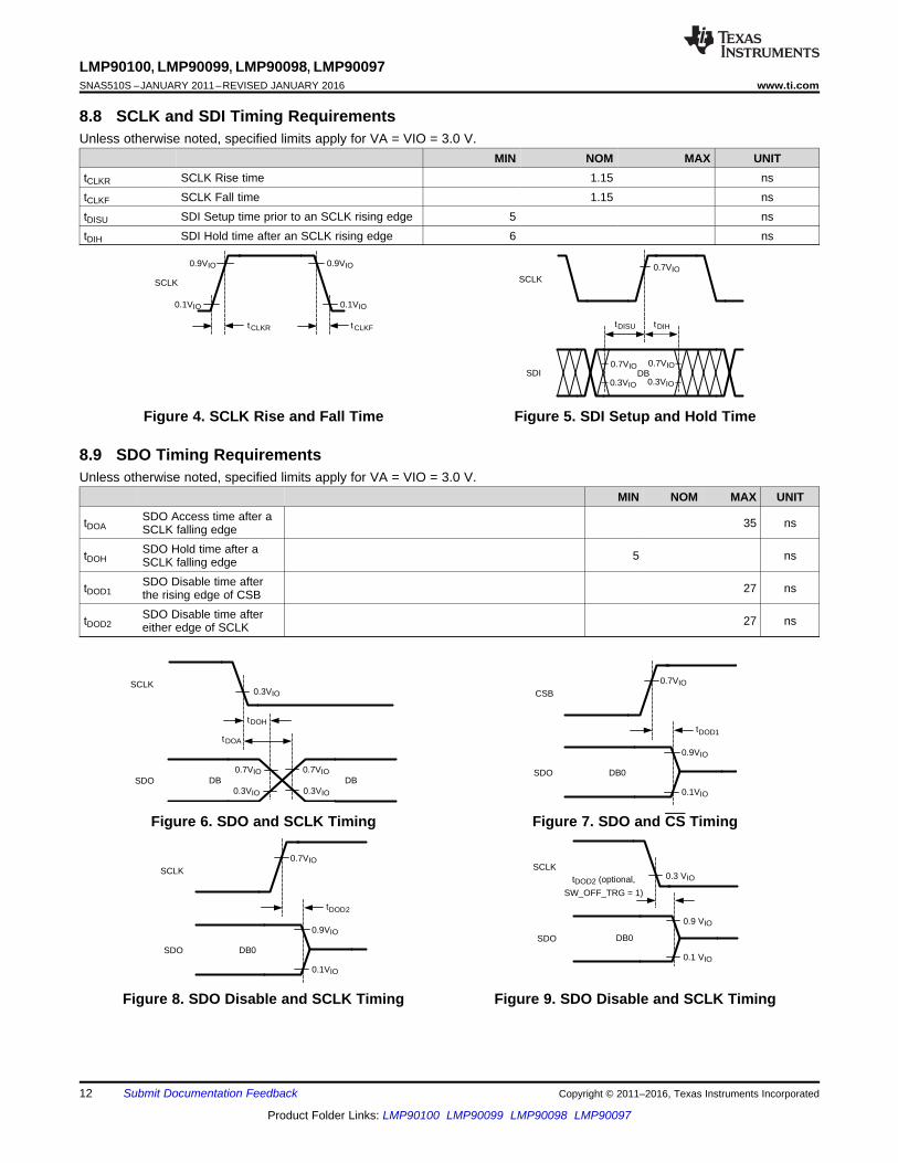
8.8 SCLK and SDI Timing RequirementsUnless otherwise noted, specified limits apply for VA = VIO = 3.0 V.
MIN NOM MAX UNITtCLKR SCLK Rise time 1.15 nstCLKF SCLK Fall time 1.15 nstDISU SDI Setup time prior to an SCLK rising edge 5 nstDIH SDI Hold time after an SCLK rising edge 6 ns
Figure 4. SCLK Rise and Fall Time Figure 5. SDI Setup and Hold Time
8.9 SDO Timing RequirementsUnless otherwise noted, specified limits apply for VA = VIO = 3.0 V.
MIN NOM MAX UNIT
tDOASDO Access time after aSCLK falling edge 35 ns
tDOHSDO Hold time after aSCLK falling edge 5 ns
tDOD1SDO Disable time afterthe rising edge of CSB 27 ns
tDOD2SDO Disable time aftereither edge of SCLK 27 ns
Figure 6. SDO and SCLK Timing Figure 7. SDO and CS Timing
Figure 8. SDO Disable and SCLK Timing Figure 9. SDO Disable and SCLK Timing

SCLK
SDO
8 9
0.3VIO
0.7VIO
tDOE
DB7
0.3VIO SDO
0.9VIO
0.1VIO
tDOFtDOR
0.1VIO
0.9VIO
13
LMP90100, LMP90099, LMP90098, LMP90097www.ti.com SNAS510S –JANUARY 2011–REVISED JANUARY 2016
Product Folder Links: LMP90100 LMP90099 LMP90098 LMP90097
Submit Documentation FeedbackCopyright © 2011–2016, Texas Instruments Incorporated
(1) This parameter is specified by design and/or characterization and is not tested in production
8.10 SDO and DRDYB Timing RequirementsUnless otherwise noted, specified limits apply for VA = VIO = 3.0 V.
MIN NOM MAX UNITtDOE SDO Enable time from the falling edge of the 8th SCLK 35 nstDOR SDO Rise time See (1) 7 nstDOF SDO Fall time See (1) 7 ns
tDRDYB
Data Ready Bar pulse atevery1/ODR second, seeFigure 62
ODR ≤ 13.42 SPS 64
µs13.42 < ODR ≤ 214.65 SPS 4
Figure 10. SDO and SCLK Enable Timing Figure 11. SDO Rise and Fall Timing
0 200 400 600 800 1000
0
5
10
15
20
25
30
35
40
VO
UT
(�
V)
TIME (ms)
VA = 3V
0 200 400 600 800 1000
-20
-15
-10
-5
0
5
10
15
20
VO
UT
(�
V)
TIME (ms)
VA = 3V
150 170 190 210 230 2500
200
400
600
800
1000
1200
1400
1600
CO
UN
T
VOUT (PV)
VA = 3V
-50 -30 -10 10 30 500
200
400
600
800
1000
1200
1400
1600
CO
UN
T
VOUT (PV)
VA = 3V
0 200 400 600 800 1000150
170
190
210
230
250
VO
UT
(�
V)
TIME (ms)
VA = 3V
0 200 400 600 800 1000-50
-30
-10
10
30
50
VO
UT
(�
V)
TIME (ms)
VA = 3V
14
LMP90100, LMP90099, LMP90098, LMP90097SNAS510S –JANUARY 2011–REVISED JANUARY 2016 www.ti.com
Product Folder Links: LMP90100 LMP90099 LMP90098 LMP90097
Submit Documentation Feedback Copyright © 2011–2016, Texas Instruments Incorporated
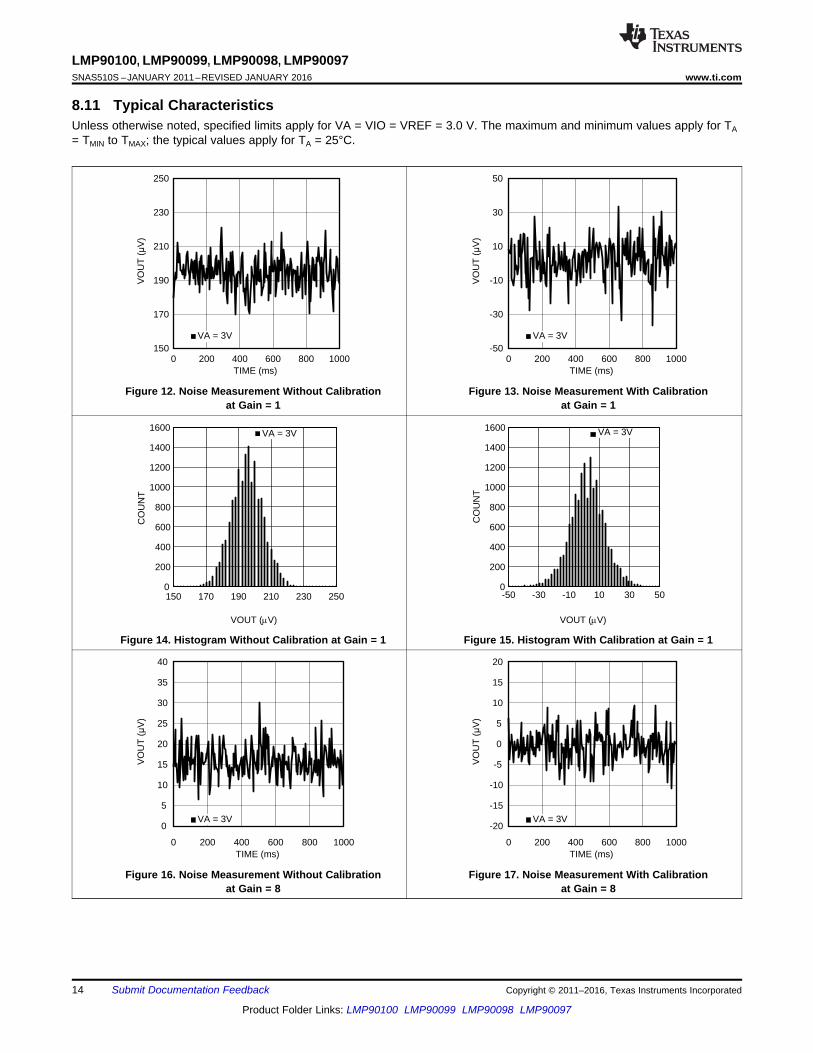
8.11 Typical CharacteristicsUnless otherwise noted, specified limits apply for VA = VIO = VREF = 3.0 V. The maximum and minimum values apply for TA= TMIN to TMAX; the typical values apply for TA = 25°C.
Figure 12. Noise Measurement Without Calibrationat Gain = 1
Figure 13. Noise Measurement With Calibrationat Gain = 1
Figure 14. Histogram Without Calibration at Gain = 1 Figure 15. Histogram With Calibration at Gain = 1
Figure 16. Noise Measurement Without Calibrationat Gain = 8
Figure 17. Noise Measurement With Calibrationat Gain = 8
-5 -3 -1 1 3 50
500
1000
1500
2000
2500
3000
CO
UN
T
VOUT (PV)
VA = 3V
-5 -3 -1 1 3 50
500
1000
1500
2000
2500
3000
CO
UN
T
VOUT (PV)
VA = 3V
0 200 400 600 800 1000
-4
-3
-2
-1
0
1
2
3
4
VO
UT
(�
V)
TIME (ms)
VA = 3V
0 200 400 600 800 1000
-4
-3
-2
-1
0
1
2
3
4
VO
UT
(�
V)
TIME (ms)
VA = 3V
-25 -15 -5 5 15 25 350
500
1000
1500
2000
CO
UN
T
VOUT (PV)
VA = 3V
-25 -15 -5 5 15 25 350
500
1000
1500
2000
CO
UN
T
VOUT (µV)
VA = 3V
15
LMP90100, LMP90099, LMP90098, LMP90097www.ti.com SNAS510S –JANUARY 2011–REVISED JANUARY 2016
Product Folder Links: LMP90100 LMP90099 LMP90098 LMP90097
Submit Documentation FeedbackCopyright © 2011–2016, Texas Instruments Incorporated
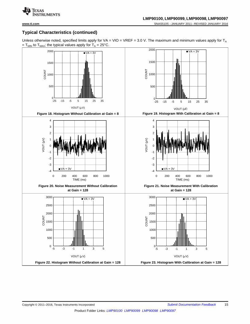
Typical Characteristics (continued)Unless otherwise noted, specified limits apply for VA = VIO = VREF = 3.0 V. The maximum and minimum values apply for TA= TMIN to TMAX; the typical values apply for TA = 25°C.
Figure 18. Histogram Without Calibration at Gain = 8 Figure 19. Histogram With Calibration at Gain = 8
Figure 20. Noise Measurement Without Calibrationat Gain = 128
Figure 21. Noise Measurement With Calibrationat Gain = 128
Figure 22. Histogram Without Calibration at Gain = 128 Figure 23. Histogram With Calibration at Gain = 128

1 2 4 8 16 32 64 12815
16
17
18
19
20
21
EN
OB
(bi
ts)
GAIN
VA = 3VVA = 5V
1 2 4 8 16 32 64 12815
16
17
18
19
20
21
EN
OB
(bi
ts)
GAIN
VA = 3VVA = 5V
1 2 4 8 16 32 64 1280
2
4
6
8
10
12
RM
S N
OIS
E (#V)
GAIN
VA = 3VVA = 5V
1 2 4 8 16 32 64 1280
2
4
6
8
10
12
RM
S N
OIS
E (#V)
GAIN
VA = 3VVA = 5V
1 2 4 8 16 32 64 12815
16
17
18
19
20
21
EN
OB
(bi
ts)
GAIN
VA = 3VVA = 5V
1 2 4 8 16 32 64 12815
16
17
18
19
20
21
EN
OB
(bi
ts)
GAIN
VA = 3VVA = 5V
16
LMP90100, LMP90099, LMP90098, LMP90097SNAS510S –JANUARY 2011–REVISED JANUARY 2016 www.ti.com
Product Folder Links: LMP90100 LMP90099 LMP90098 LMP90097
Submit Documentation Feedback Copyright © 2011–2016, Texas Instruments Incorporated
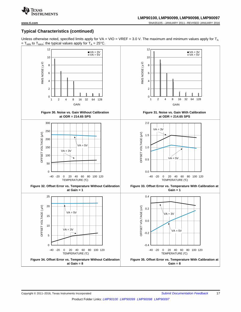
Typical Characteristics (continued)Unless otherwise noted, specified limits apply for VA = VIO = VREF = 3.0 V. The maximum and minimum values apply for TA= TMIN to TMAX; the typical values apply for TA = 25°C.
Figure 24. ENOB vs. Gain Without Calibrationat ODR = 13.42 SPS
Figure 25. ENOB vs. Gain With Calibrationat ODR = 13.42 SPS
Figure 26. Noise vs. Gain Without Calibrationat ODR = 13.42 SPS
Figure 27. Noise vs. Gain With Calibrationat ODR = 13.42 SPS
Figure 28. ENOB vs. Gain Without Calibrationat ODR = 214.65 SPS
Figure 29. ENOB vs. Gain With Calibrationat ODR = 214.65 SPS
-40 -20 0 20 40 60 80 100 120
0
5
10
15
20
25
OF
FS
ET
VO
LTA
GE
( �
V)
TEMPERATURE (°C)
VA = 5V
VA = 3V
-40 -20 0 20 40 60 80 100 120
-0.4
-0.2
0.0
0.2
0.4
OF
FS
ET
VO
LTA
GE
(uV
)
TEMPERATURE (°C)
VA = 5V
VA = 3V
-40 -20 0 20 40 60 80 100 120
0
50
100
150
200
250
300
OF
FS
ET
VO
LTA
GE
(�
V)
TEMPERATURE (°C)
VA = 3V
VA = 5V
-40 -20 0 20 40 60 80 100 120
0.0
0.5
1.0
1.5
2.0
OF
FS
ET
VO
LTA
GE
(�
V)
TEMPERATURE (°C)
VA = 3V
VA = 5V
1 2 4 8 16 32 64 1280
2
4
6
8
10
12
RM
S N
OIS
E (#V)
GAIN
VA = 3VVA = 5V
1 2 4 8 16 32 64 1280
2
4
6
8
10
12
RM
S N
OIS
E (#V)
GAIN
VA = 3VVA = 5V
17
LMP90100, LMP90099, LMP90098, LMP90097www.ti.com SNAS510S –JANUARY 2011–REVISED JANUARY 2016
Product Folder Links: LMP90100 LMP90099 LMP90098 LMP90097
Submit Documentation FeedbackCopyright © 2011–2016, Texas Instruments Incorporated
Typical Characteristics (continued)Unless otherwise noted, specified limits apply for VA = VIO = VREF = 3.0 V. The maximum and minimum values apply for TA= TMIN to TMAX; the typical values apply for TA = 25°C.
Figure 30. Noise vs. Gain Without Calibrationat ODR = 214.65 SPS
Figure 31. Noise vs. Gain With Calibrationat ODR = 214.65 SPS
Figure 32. Offset Error vs. Temperature Without Calibrationat Gain = 1
Figure 33. Offset Error vs. Temperature With Calibration atGain = 1
Figure 34. Offset Error vs. Temperature Without Calibrationat Gain = 8
Figure 35. Offset Error vs. Temperature With Calibration atGain = 8

1 10 100
-120
-100
-80
-60
-40
-20
0
GA
IN (
dB)
FREQUENCY (Hz)
1.7 SPS3.4 SPS6.7 SPS13.4 SPS
10 100 1k
-120
-100
-80
-60
-40
-20
0
GA
IN (
dB)
FREQUENCY (Hz)
26.83 SPS53.66 SPS107.33 SPS214.65 SPS
-40 -20 0 20 40 60 80 100 120
-160
-150
-140
-130
-120
-110
-100
GA
IN E
RR
OR
(pp
m)
TEMPERATURE (°C)
VA = 5V
VA = 3V
-40 -20 0 20 40 60 80 100 120
-120
-100
-80
-60
-40
-20
GA
IN E
RR
OR
(pp
m)
TEMPERATURE (°C)
VA = 3V
VA = 5V
-40 -20 0 20 40 60 80 100 120
110
120
130
140
150
160
GA
IN E
RR
OR
(pp
m)
TEMPERATURE (°C)
VA = 5V
VA = 3V
-40 -20 0 20 40 60 80 100 120
-40
-20
0
20
40
GA
IN E
RR
OR
(pp
m)
TEMPERATURE (°C)
VA = 5V
VA = 3V
18
LMP90100, LMP90099, LMP90098, LMP90097SNAS510S –JANUARY 2011–REVISED JANUARY 2016 www.ti.com
Product Folder Links: LMP90100 LMP90099 LMP90098 LMP90097
Submit Documentation Feedback Copyright © 2011–2016, Texas Instruments Incorporated
Typical Characteristics (continued)Unless otherwise noted, specified limits apply for VA = VIO = VREF = 3.0 V. The maximum and minimum values apply for TA= TMIN to TMAX; the typical values apply for TA = 25°C.
Figure 36. Gain Error vs. Temperature Without Calibrationat Gain = 1
Figure 37. Gain Error vs. Temperature With Calibrationat Gain = 1
Figure 38. Gain Error vs. Temperature Without Calibrationat Gain = 8
Figure 39. Gain Error vs. Temperature With Calibrationat Gain = 8
Figure 40. Digital Filter Frequency Response Figure 41. Digital Filter Frequency Response

-5 -4 -3 -2 -1 0 1 2 3 4 5
-10
-5
0
5
10
INL
(ppm
of F
SR
)
VIN (V)
VA = 5V, 13.4 SPS
19
LMP90100, LMP90099, LMP90098, LMP90097www.ti.com SNAS510S –JANUARY 2011–REVISED JANUARY 2016
Product Folder Links: LMP90100 LMP90099 LMP90098 LMP90097
Submit Documentation FeedbackCopyright © 2011–2016, Texas Instruments Incorporated
Typical Characteristics (continued)Unless otherwise noted, specified limits apply for VA = VIO = VREF = 3.0 V. The maximum and minimum values apply for TA= TMIN to TMAX; the typical values apply for TA = 25°C.
Figure 42. INL at Gain = 1

VA
Internal
CLK
Ext. Clk
Detect
CLK/
XIN
XOUT
CSB
SCLK
SDI
SDO/DRDYB
VREFP1 VREFN1
VIN0
VIN1
VIN2
VIN3
VIN4
VIN5
IB1
IB2
VA
EXC.
CURRENT
GND
GPIO
D0D6/
DRDYB
Open/Short
Sensor Diag.
VIO
EXC.
CURRENT
SERIAL I/F
CONTROL
&
CALIBRATION
DATA PATH
POR
24 bit
Module
SD DIGITAL
FILTER
CLK
MUX
BUFF
VIN6/VREFP2
MUX
Chip Configurable
Channel Configurable
Fixed
LMP90xxx
BACKGROUND
CALIBRATION
PGA
1x, 2x,
4x, 8x
VIN7/VREFN2
VREF
FGA
16x
INP
UT
MU
X
LMP90100/LMP9
0098 only
LMP90100/LMP9
0099 only
20
LMP90100, LMP90099, LMP90098, LMP90097SNAS510S –JANUARY 2011–REVISED JANUARY 2016 www.ti.com
Product Folder Links: LMP90100 LMP90099 LMP90098 LMP90097
Submit Documentation Feedback Copyright © 2011–2016, Texas Instruments Incorporated
9 Detailed Description
9.1 OverviewThe LMP90xxx is a low-power 24-Bit ΣΔ ADC with 4 fully differential / 7 single-ended analog channels for theLMP90100/LMP90099 and 2 full differential / 4 single-ended for the LMP90098/LMP90097. Its serial data outputis two’s complement format. The output data rate (ODR) ranges from 1.6775 SPS to 214.65 SPS.
The serial communication for LMP90xxx is SPI, a synchronous serial interface that operates using 4 pins: chipselect bar (CSB), serial clock (SCLK), serial data in (SDI), and serial data out / data ready bar (SDO/DRYDYB).
True continuous built-in offset and gain background calibration is also available to improve measurementaccuracy. Unlike other ADCs, the LMP90xxx’s background calibration can run without heavily impacting the inputsignal. This unique technique allows for positive as well as negative gain calibration and is available at all gainsettings.
The registers can be found in Programming, and a detailed description of the LMP90xxx are provided in thefollowing sections.
9.2 Functional Block Diagram
9.3 Feature Description
9.3.1 True Continuous Background CalibrationThe LMP90100/LMP90099/LMP90098/LMP90097 feature a 24 bit ΣΔ core with continuous backgroundcalibration to compensate for gain and offset errors in the ADC, virtually eliminating any drift with time andtemperature. The calibration is performed in the background without user or ADC input interruption, making itunique in the industry and eliminating down time associated with field calibration required with other solutions.Having this continuous calibration improves performance over the entire life span of the end product.
21
LMP90100, LMP90099, LMP90098, LMP90097www.ti.com SNAS510S –JANUARY 2011–REVISED JANUARY 2016
Product Folder Links: LMP90100 LMP90099 LMP90098 LMP90097
Submit Documentation FeedbackCopyright © 2011–2016, Texas Instruments Incorporated
Feature Description (continued)9.3.2 Continuous Background Sensor DiagnosticsSensor diagnostics are also performed in the background, without interfering with signal path performance,allowing the detection of sensor shorts, opens, and out-of-range signals, which vastly improves system reliability.In addition, the fully flexible input multiplexer described below allows any input pin to be connected to any ADCinput channel providing additional sensor path diagnostic capability.
9.3.3 Flexible Input MUX ChannelsThe flexible input MUX allows interfacing to a wide range of sensors such as thermocouples, RTDs, thermistors,and bridge sensors. The LMP90100/LMP90099’s multiplexer supports 4 differential channels while theLMP90098/LMP90097 supports 2. Each effective input voltage that is digitized is VIN = VINx – VINy, where xand y are any input. In addition, the input multiplexer of the LMP90100/LMP90099 also supports 7 single-endedchannels (LMP90098/LMP90097 supports 4), where the common ground is any one of the inputs.
9.3.4 Programmable Gain Amplifiers (FGA and PGA)The LMP90100/LMP90099/LMP90098/LMP90097 contain an internal 16x fixed gain amplifier (FGA) and a 1x,2x, 4x, or 8x programmable gain amplifier (PGA). This allows accurate gain settings of 1x, 2x, 4x, 8x, 16x, 32x,64x, or 128x through configuration of internal registers. Having an internal amplifier eliminates the need forexternal amplifiers that are costly, space consuming, and difficult to calibrate.
9.3.5 Excitation Current Sources (IB1 and IB2) - LMP90100/LMP90098Two matched internal excitation currents, IB1 and IB2, can be used for sourcing currents to a variety of sensors.The current range is from 100 µA to 1000 µA in steps of 100 µA.
9.3.6 Signal Path
9.3.6.1 Reference Input (VREF)The differential reference voltage VREF (VREFP – VREFN) sets the range for VIN.
The muxed VREF allows the user to choose between VREF1 or VREF2 for each channel. This selection can bemade by programming the VREF_SEL bit in the CHx_INPUTCN registers (CHx_INPUTCN: VREF_SEL). Thedefault mode is VREF1. If VREF2 is used, then VIN6 and VIN7 cannot be used as inputs because they share thesame pin.
Refer to VREF for VREF applications information.
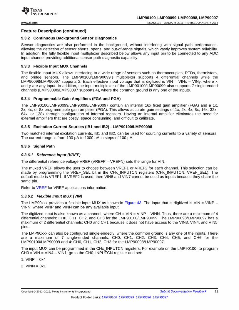
9.3.6.2 Flexible Input MUX (VIN)The LMP90xxx provides a flexible input MUX as shown in Figure 43. The input that is digitized is VIN = VINP –VINN; where VINP and VINN can be any available input.
The digitized input is also known as a channel, where CH = VIN = VINP – VINN. Thus, there are a maximum of 4differential channels: CH0, CH1, CH2, and CH3 for the LMP90100/LMP90099. The LMP90098/LMP90097 has amaximum of 2 differential channels: CH0 and CH1 because it does not have access to the VIN3, VIN4, and VIN5pins.
The LMP90xxx can also be configured single-endedly, where the common ground is any one of the inputs. Thereare a maximum of 7 single-ended channels: CH0, CH1, CH2, CH3, CH4, CH5, and CH6 for theLMP90100/LMP90099 and 4: CH0, CH1, CH2, CH3 for the LMP90098/LMP90097.
The input MUX can be programmed in the CHx_INPUTCN registers. For example on the LMP90100, to programCH0 = VIN = VIN4 – VIN1, go to the CH0_INPUTCN register and set:
1. VINP = 0x4
2. VINN = 0x1
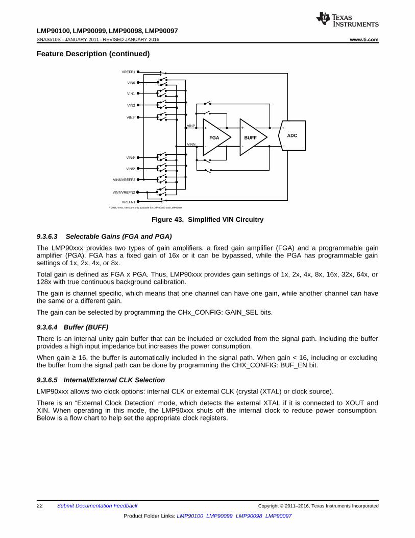
VIN2
VIN4*
VIN3*
VREFN1
VIN6/VREFP2
ADC
VREFP1
+
-
+
-
+
-
VIN0
VIN5*
VIN1
VIN7/VREFN2
VINP
VINN
BUFFFGA
* VIN3, VIN4, VIN5 are only available for LMP90100 and LMP90099
22
LMP90100, LMP90099, LMP90098, LMP90097SNAS510S –JANUARY 2011–REVISED JANUARY 2016 www.ti.com
Product Folder Links: LMP90100 LMP90099 LMP90098 LMP90097
Submit Documentation Feedback Copyright © 2011–2016, Texas Instruments Incorporated
Feature Description (continued)
Figure 43. Simplified VIN Circuitry
9.3.6.3 Selectable Gains (FGA and PGA)The LMP90xxx provides two types of gain amplifiers: a fixed gain amplifier (FGA) and a programmable gainamplifier (PGA). FGA has a fixed gain of 16x or it can be bypassed, while the PGA has programmable gainsettings of 1x, 2x, 4x, or 8x.
Total gain is defined as FGA x PGA. Thus, LMP90xxx provides gain settings of 1x, 2x, 4x, 8x, 16x, 32x, 64x, or128x with true continuous background calibration.
The gain is channel specific, which means that one channel can have one gain, while another channel can havethe same or a different gain.
The gain can be selected by programming the CHx_CONFIG: GAIN_SEL bits.
9.3.6.4 Buffer (BUFF)There is an internal unity gain buffer that can be included or excluded from the signal path. Including the bufferprovides a high input impedance but increases the power consumption.
When gain ≥ 16, the buffer is automatically included in the signal path. When gain < 16, including or excludingthe buffer from the signal path can be done by programming the CHX_CONFIG: BUF_EN bit.
9.3.6.5 Internal/External CLK SelectionLMP90xxx allows two clock options: internal CLK or external CLK (crystal (XTAL) or clock source).
There is an “External Clock Detection” mode, which detects the external XTAL if it is connected to XOUT andXIN. When operating in this mode, the LMP90xxx shuts off the internal clock to reduce power consumption.Below is a flow chart to help set the appropriate clock registers.

ClockOptions
Connect a XTAL to XIN and XOUT
Connect an external CLK source to the
XIN/CLK pin
Is there a XTAL connected to XIN and
XOUT?
Set CLK_EXT_DET = 1 to E\SDVV�WKH�³([WHUQDO-Clock
'HWHFWLRQ´�PRGH
Yes
Set CLK_SEL = 0 to select the internal clock
LMP90100 will use the internal clock
No
LMP90100 will automatically detect and use the XTAL if CLK_EXT_DET = 0
(default)
Internal CLK
ExternalXTAL
External CLK Source
LMP90100 will automatically use the external CLK source
23
LMP90100, LMP90099, LMP90098, LMP90097www.ti.com SNAS510S –JANUARY 2011–REVISED JANUARY 2016
Product Folder Links: LMP90100 LMP90099 LMP90098 LMP90097
Submit Documentation FeedbackCopyright © 2011–2016, Texas Instruments Incorporated
Feature Description (continued)
Figure 44. CLK Register Settings
The recommended value for the external CLK is discussed in the next sections.
9.3.6.6 Programmable ODRsIf using the internal CLK or external CLK of 3.5717 MHz, then the output date rates (ODR) can be selected(using the ODR_SEL bit) as:
1. 13.42/8 = 1.6775 SPS
2. 13.42/4 = 3.355 SPS
3. 13.42/2 = 6.71SPS
4. 13.42 SPS
5. 214.65/8 = 26.83125 SPS
6. 214.65/4 = 53.6625 SPS
7. 214.65/2 = 107.325 SPS
8. 214.65 SPS (default)
If the internal CLK is not being used and the external CLK is not 3.5717 MHz, then the ODR will be different. Ifthis is the case, use the equation below to calculate the new ODR values.
ODR_Base1 = (CLKEXT) / (266,240) (1)ODR_Base2 = (CLKEXT) / (16,640) (2)ODR1 = (ODR_Base1) / n
where• n = 1,2,4,8 (3)
ODR2 = (ODR_Base2) / n
where• n = 1,2,4,8 (4)
For example, a 3.6864 MHz XTAL or external clock has the following ODR values:ODR_Base1 = (3.6864 MHz) / (266,240) = 13.85 SPS (5)ODR_Base2 = (3.6864 MHz) / (16,640) = 221.54 SPS (6)ODR1 = (13.85 SPS) / n = 13.85, 6.92, 3.46, 1.73 SPS (7)

40 45 50 55 60 65 70
-140
-120
-100
-80
-60
-40
-20
0
GA
IN (
dB)
FREQUENCY (Hz)
Crystal = 3.5717 MHzCrystal = 3.6864 MHz
0 200 400 600 800 1000 1200 1400 1600 1800 2000
-120
-80
-40
0
GA
IN (
dB)
FREQUENCY (Hz)
107.325 SPS214.65 SPS
45 47 49 51 53 55 57 59 61 63 65
-120
-110
-100
-90
-80
-70
-60
GA
IN (
dB)
FREQUENCY (Hz)
13.42 SPS
0 200 400 600 800 1000 1200 1400 1600 1800 2000
-120
-80
-40
0
GA
IN (
dB)
FREQUENCY (Hz)
26.83125 SPS53.6625 SPS
0 12 24 36 48 60 72 84 96 108 120
-120
-100
-80
-60
-40
-20
0
GA
IN (
dB)
FREQUENCY (Hz)
1.6775 SPS3.355 SPS
0 12 24 36 48 60 72 84 96 108 120
-120
-100
-80
-60
-40
-20
0
GA
IN (
dB)
FREQUENCY (Hz)
6.71 SPS13.42 SPS
24
LMP90100, LMP90099, LMP90098, LMP90097SNAS510S –JANUARY 2011–REVISED JANUARY 2016 www.ti.com
Product Folder Links: LMP90100 LMP90099 LMP90098 LMP90097
Submit Documentation Feedback Copyright © 2011–2016, Texas Instruments Incorporated
Feature Description (continued)ODR2 = (221.54 SPS) / n = 221.54, 110.77, 55.38, 27.69 SPS (8)
The ODR is channel specific, which means that one channel can have one ODR, while another channel canhave the same or a different ODR.
Note that these ODRs are meant for a single channel conversion; the ODR needs to be divided by n for nchannels scanning. For example, if the ADC were running at 214.65 SPS and four channels are being scanned,then the ODR per channel would be 214.65/4 = 53.6625 SPS.
9.3.6.7 Digital FilterThe LMP90xxx has a fourth order rotated sinc filter that is used to configure various ODRs and to reject powersupply frequencies of 50Hz and 60Hz. The 50/60 Hz rejection is only effective when the device is operating atODR ≤ 13.42 SPS. If the internal CLK or the external CLK of 3.5717 MHz is used, then the LMP90xxx will havethe frequency response shown in Figure 45 to Figure 49.
Figure 45. Digital Filter Response, 1.6775 SPS and 3.355SPS
Figure 46. Digital Filter Response, 6.71 SPS and 13.42 SPS
Figure 47. Digital Filter Response at 13.42 SPS Figure 48. Digital Filter Response, 26.83125 SPS and53.6625 SPS
Figure 49. Digital Filter Response 107.325 SPS and 214.65SPS
Figure 50. Digital Filter Response for a 3.5717 MHz versus3.6864 MHz XTAL

Calibration
Background calibration
System calibration
Correction Estimation Offset Gain
PinsD0 ± D6 =
Set GPIO_DIRCNx = 0
Set GPIO_DIRCNx = 1
Write to GPIO_DAT: Dx bit to drive Dx high or low,
where 0 ��[���6.
inputs outputs
Read theGPIO_DAT: Dx bit to
determine if Dx is high or low, where
0 ��[���6.
25
LMP90100, LMP90099, LMP90098, LMP90097www.ti.com SNAS510S –JANUARY 2011–REVISED JANUARY 2016
Product Folder Links: LMP90100 LMP90099 LMP90098 LMP90097
Submit Documentation FeedbackCopyright © 2011–2016, Texas Instruments Incorporated
Feature Description (continued)If the internal CLK is not being used and the external CLK is not 3.5717 MHz, then the filter response would bethe same as the response shown in Figure 49, but the frequency will change according to the equation:
fNEW = [(CLKEXT) / 256 ] x (fOLD / 13.952k) (9)
Using Equation 9, an example of the filter response for a 3.5717 MHz XTAL versus a 3.6864 MHz XTAL can beseen in Figure 50.
9.3.6.8 GPIO (D0–D6)Pins D0-D6 are general-purpose input/output (GPIO) pins that can be used to control external LEDs or switches.Only a high or low value can be sourced to or read from each pin.
Figure 51 shows a flow chart how these GPIOs can be programmed.
Figure 51. GPIO Register Settings
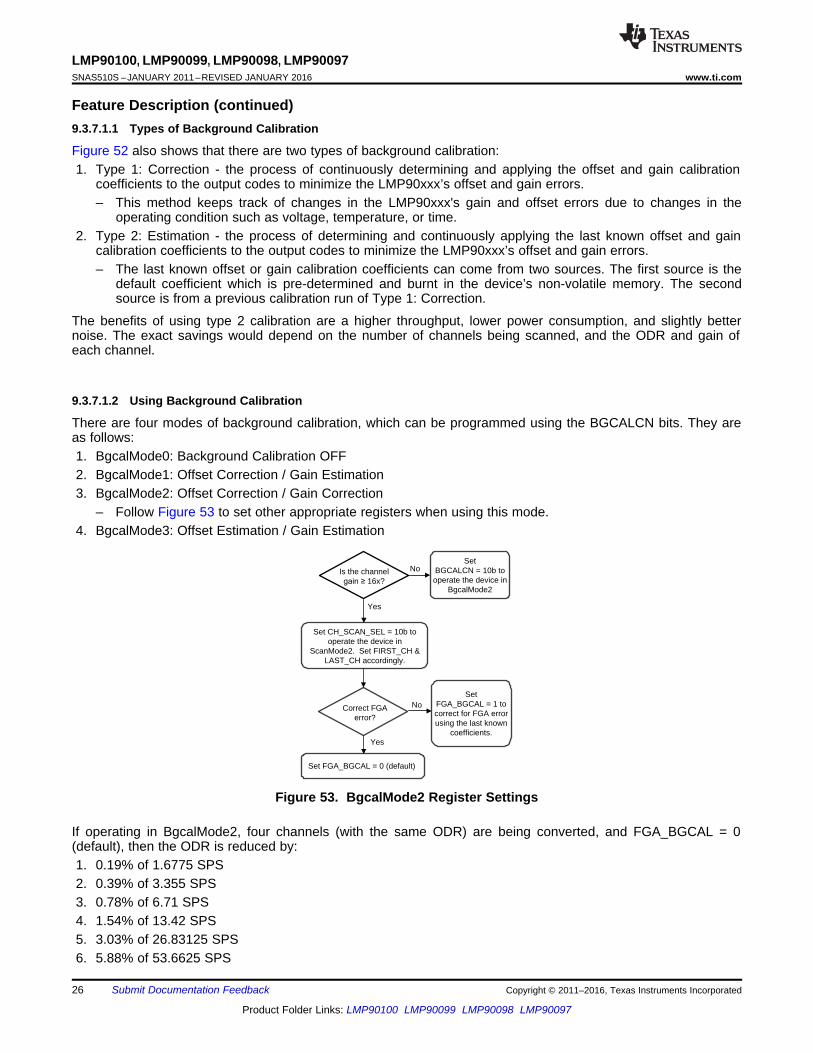
9.3.7 CalibrationAs seen in Figure 52, there are two types of calibration: background calibration and system calibration. Thesecalibrations are further described in the next sections.
Figure 52. Types of Calibration
9.3.7.1 Background CalibrationBackground calibration is the process of continuously determining and applying the offset and gain calibrationcoefficients to the output codes to minimize the LMP90xxx’s offset and gain errors. Background calibration is afeature built into the LMP90xxx and is automatically done by the hardware without interrupting the input signal.
Four differential channels, CH0-CH3, each with its own gain and ODRs, can be calibrated to improve theaccuracy.
Yes
Set BGCALCN = 10b to operate the device in
BgcalMode2
NoIs the channel JDLQ���16x?
Set CH_SCAN_SEL = 10b to operate the device in
ScanMode2. Set FIRST_CH & LAST_CH accordingly.
Set FGA_BGCAL = 0 (default)
Correct FGA error?
Yes
NoSet
FGA_BGCAL = 1 to correct for FGA error using the last known
coefficients.
26
LMP90100, LMP90099, LMP90098, LMP90097SNAS510S –JANUARY 2011–REVISED JANUARY 2016 www.ti.com
Product Folder Links: LMP90100 LMP90099 LMP90098 LMP90097
Submit Documentation Feedback Copyright © 2011–2016, Texas Instruments Incorporated
Feature Description (continued)9.3.7.1.1 Types of Background Calibration
Figure 52 also shows that there are two types of background calibration:1. Type 1: Correction - the process of continuously determining and applying the offset and gain calibration
coefficients to the output codes to minimize the LMP90xxx’s offset and gain errors.– This method keeps track of changes in the LMP90xxx's gain and offset errors due to changes in the
operating condition such as voltage, temperature, or time.2. Type 2: Estimation - the process of determining and continuously applying the last known offset and gain
calibration coefficients to the output codes to minimize the LMP90xxx’s offset and gain errors.– The last known offset or gain calibration coefficients can come from two sources. The first source is the
default coefficient which is pre-determined and burnt in the device’s non-volatile memory. The secondsource is from a previous calibration run of Type 1: Correction.
The benefits of using type 2 calibration are a higher throughput, lower power consumption, and slightly betternoise. The exact savings would depend on the number of channels being scanned, and the ODR and gain ofeach channel.
9.3.7.1.2 Using Background Calibration
There are four modes of background calibration, which can be programmed using the BGCALCN bits. They areas follows:1. BgcalMode0: Background Calibration OFF2. BgcalMode1: Offset Correction / Gain Estimation3. BgcalMode2: Offset Correction / Gain Correction
– Follow Figure 53 to set other appropriate registers when using this mode.4. BgcalMode3: Offset Estimation / Gain Estimation
Figure 53. BgcalMode2 Register Settings
If operating in BgcalMode2, four channels (with the same ODR) are being converted, and FGA_BGCAL = 0(default), then the ODR is reduced by:1. 0.19% of 1.6775 SPS2. 0.39% of 3.355 SPS3. 0.78% of 6.71 SPS4. 1.54% of 13.42 SPS5. 3.03% of 26.83125 SPS6. 5.88% of 53.6625 SPS

y
OFFSET[CHx_SCAL_
OFFSET]
UncalibratedVIN
CalibratedADC_DOUT
GAIN[CHx_SCAL_
GAIN]
±
27
LMP90100, LMP90099, LMP90098, LMP90097www.ti.com SNAS510S –JANUARY 2011–REVISED JANUARY 2016
Product Folder Links: LMP90100 LMP90099 LMP90098 LMP90097
Submit Documentation FeedbackCopyright © 2011–2016, Texas Instruments Incorporated
Feature Description (continued)7. 11.11% of 107.325 SPS8. 20% of 214.65 SPS
9.3.7.2 System CalibrationThe LMP90xxx provides some unique features to support easy system offset and system gain calibrations.
The System Calibration Offset Registers (CHx_SCAL_OFFSET) hold the System Calibration Offset Coefficientsin 24-bit, two's complement binary format. The System Calibration Gain Registers (CHx_SCAL_GAIN) hold theSystem Calibration Gain Coefficient in 24-bit, 1.23, unsigned, fixed-point binary format. For each channel, theSystem Calibration Offset coefficient is subtracted from the conversion result prior to the division by the SystemCalibration Gain Coefficient.
A data-flow diagram of these coefficients can be seen in Figure 54.
Figure 54. System Calibration Data-Flow Diagram
There are four distinct sets of System Calibration Offset and System Calibration Gain Registers for use withCH0-CH3. CH4-CH6 reuse the registers of CH0-CH2, respectively.
The LMP90xxx provides two system calibration modes that automatically fill the Offset and Gain coefficients foreach channel. These modes are the System Calibration Offset Coefficient Determination mode and the SystemCalibration Gain Coefficient Determination mode. The System Calibration Offset Coefficient Determination modemust be entered prior to the System Calibration Gain Coefficient Determination mode, for each channel.
The system zero-scale condition is a system input condition (sensor loading) for which zero (0x00_0000) system-calibrated output code is desired. It may not, however, cause a zero input voltage at the input of the ADC.
The system reference-scale condition is usually the system full-scale condition in which the system's input (orsensor's loading) would be full-scale and the desired system-calibrated output code would be 0x80_0000(unsigned 24-bit binary). However, system full-scale condition need not cause full-scale input voltage at the inputof the ADC.
The system reference-scale condition is not restricted to just the system full-scale condition. In fact, it can be anyarbitrary fraction of full-scale (up to 1.25 times) and the desired system-calibrated output code can be anyappropriate value (up to 0xA00000). The CHx_SCAL_GAIN register must be written with the desired system-calibrated output code (default:0x800000) before entering the System Calibration Gain Coefficient Determinationmode. This helps in in-place system calibration.
Below are the detailed procedures for using the System Calibration Offset Coefficient Determination and SystemCalibration Gain Coefficient Determination modes.
9.3.7.2.1 System Calibration Offset Coefficient Determination Mode1. Apply system zero-scale condition to the channel (CH0/CH1/CH2/CH3).2. Enter the System Calibration Offset Coefficient Determination mode by programming 0x1 in the SCALCN
register.3. LMP90xxx starts a fresh conversion at the selected output data rate for the selected channel. At the end of
the conversion, the CHx_SCAL_OFFSET register is filled-in with the System Calibration Offset coefficient.4. The System Calibration Offset Coefficient Determination mode is automatically exited.5. The computed calibration coefficient is accurate only to the effective resolution of the device and will
probably contain some noise. The noise factor can be minimized by computing over many times, averaging
SCALING[CHx_SCAL_
SCALING]
System CalibratedCode[23:0]
Scaled and CalibratedADC_DOUT
BITS SELECTOR[CHx_SCAL_
BITS_SELECTOR]
X[28:0]
28
LMP90100, LMP90099, LMP90098, LMP90097SNAS510S –JANUARY 2011–REVISED JANUARY 2016 www.ti.com
Product Folder Links: LMP90100 LMP90099 LMP90098 LMP90097
Submit Documentation Feedback Copyright © 2011–2016, Texas Instruments Incorporated
Feature Description (continued)(externally) and putting the resultant value back into the register. Alternatively, select the output data rate tobe 26.83 sps or 1.67 sps.
9.3.7.2.2 System Calibration Gain Coefficient Determination Mode1. Repeat the System Calibration Offset Coefficient Determination mode to calibrate for the channel's system
offset.2. Apply the system reference-scale condition to the channel CH0/CH1/CH2/CH3.3. In the CHx_SCAL_GAIN Register, program the expected (desired) system-calibrated output code for this
condition in 24-bit unsigned format.4. Enter the System Calibration Gain Coefficient Determination mode by programming 0x3 in the SCALCN
register.5. LMP90xxx starts a fresh conversion at the selected output data rate for the channel. At the end of the
conversion, the CHx_SCAL_GAIN is filled-in (or overwritten) with the System Calibration Gain coefficient.6. The System Calibration Gain Coefficient Determination mode is automatically exited.7. The computed calibration coefficient is accurate only to the effective resolution of the device and will
probably contain some noise. The noise factor can be minimized by computing over many times, averaging(externally) and putting the resultant value back into the register. Alternatively, select the output data rate tobe 26.83 sps or 1.67 sps.
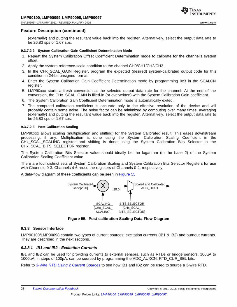
9.3.7.2.3 Post-Calibration Scaling
LMP90xxx allows scaling (multiplication and shifting) for the System Calibrated result. This eases downstreamprocessing, if any. Multiplication is done using the System Calibration Scaling Coefficient in theCHx_SCAL_SCALING register and shifting is done using the System Calibration Bits Selector in theCHx_SCAL_BITS_SELECTOR register.
The System Calibration Bits Selector value should ideally be the logarithm (to the base 2) of the SystemCalibration Scaling Coefficient value.
There are four distinct sets of System Calibration Scaling and System Calibration Bits Selector Registers for usewith Channels 0-3. Channels 4-6 reuse the registers of Channels 0-2, respectively.
A data-flow diagram of these coefficients can be seen in Figure 55
Figure 55. Post-calibration Scaling Data-Flow Diagram
9.3.8 Sensor InterfaceLMP90100/LMP90098 contain two types of current sources: excitation currents (IB1 & IB2) and burnout currents.They are described in the next sections.
9.3.8.1 IB1 and IB2 - Excitation CurrentsIB1 and IB2 can be used for providing currents to external sensors, such as RTDs or bridge sensors. 100µA to1000µA, in steps of 100µA, can be sourced by programming the ADC_AUXCN: RTD_CUR_SEL bits.
Refer to 3-Wire RTD Using 2 Current Sources to see how IB1 and IB2 can be used to source a 3-wire RTD.
Burnout Current = 10 PA
VINP
VINN
VIN0
VIN1
VIN2
VIN3*
VIN4*
VIN5*
VIN6/VREFP2
VIN7/VREFN2
Burnout Current = 10 PA
* VIN3, VIN4, VIN5 are only available for LMP90100 and LMP90099
29
LMP90100, LMP90099, LMP90098, LMP90097www.ti.com SNAS510S –JANUARY 2011–REVISED JANUARY 2016
Product Folder Links: LMP90100 LMP90099 LMP90098 LMP90097
Submit Documentation FeedbackCopyright © 2011–2016, Texas Instruments Incorporated
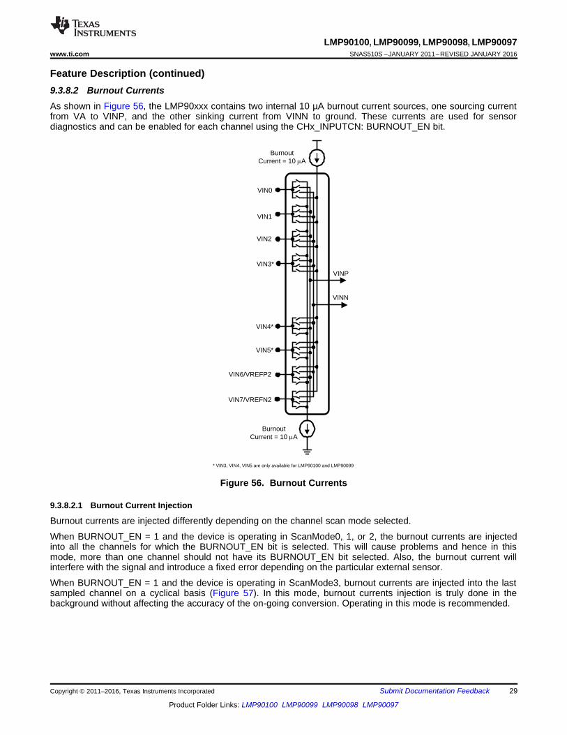
Feature Description (continued)9.3.8.2 Burnout CurrentsAs shown in Figure 56, the LMP90xxx contains two internal 10 µA burnout current sources, one sourcing currentfrom VA to VINP, and the other sinking current from VINN to ground. These currents are used for sensordiagnostics and can be enabled for each channel using the CHx_INPUTCN: BURNOUT_EN bit.
Figure 56. Burnout Currents
9.3.8.2.1 Burnout Current Injection
Burnout currents are injected differently depending on the channel scan mode selected.
When BURNOUT_EN = 1 and the device is operating in ScanMode0, 1, or 2, the burnout currents are injectedinto all the channels for which the BURNOUT_EN bit is selected. This will cause problems and hence in thismode, more than one channel should not have its BURNOUT_EN bit selected. Also, the burnout current willinterfere with the signal and introduce a fixed error depending on the particular external sensor.
When BURNOUT_EN = 1 and the device is operating in ScanMode3, burnout currents are injected into the lastsampled channel on a cyclical basis (Figure 57). In this mode, burnout currents injection is truly done in thebackground without affecting the accuracy of the on-going conversion. Operating in this mode is recommended.

FGA
Overflow detection
RAILS_FLAG
OFLO_FLAGS
ADC_DOUT
SENDIAG_THLDHand SENDIAG_THLDL
FilterBUFF Modulator
SHORT_THLD_FLAG
RAILS_FLAG
VINP
VINN
RAILS_FLAGGenerator
RAILS_FLAGGenerator
CH1 CH2 CH3CH0
CH1 CH2 CH3CH0
CH1 CH2 CH3CH0
CH1 CH2 CH3CH0
CH0 is being sampled
CH1 is being sampled
CH2 is being sampled
CH3 is being sampled
BURNOUT_EN
BURNOUT_EN
BURNOUT_EN
Burnout Currents
BURNOUT_EN
30
LMP90100, LMP90099, LMP90098, LMP90097SNAS510S –JANUARY 2011–REVISED JANUARY 2016 www.ti.com
Product Folder Links: LMP90100 LMP90099 LMP90098 LMP90097
Submit Documentation Feedback Copyright © 2011–2016, Texas Instruments Incorporated
Feature Description (continued)
Figure 57. Burnout Currents Injection for ScanMode3
9.3.8.3 Sensor Diagnostic FlagsBurnout currents can be used to verify that an external sensor is still operational before attempting to makemeasurements on that channel. A non-operational sensor means that there is a possibility the connectionbetween the sensor and the LMP90xxx is open circuited, short circuited, shorted to VA or GND, overloaded, orthe reference may be absent. The sensor diagnostic flags diagram can be seen in Figure 58.
Figure 58. Sensor Diagnostic Flags Diagram
The sensor diagnostic flags are located in the SENDIAG_FLAGS register and are described in further detailsbelow.

31
LMP90100, LMP90099, LMP90098, LMP90097www.ti.com SNAS510S –JANUARY 2011–REVISED JANUARY 2016
Product Folder Links: LMP90100 LMP90099 LMP90098 LMP90097
Submit Documentation FeedbackCopyright © 2011–2016, Texas Instruments Incorporated
Feature Description (continued)9.3.8.3.1 SHORT_THLD_FLAG
The short circuit threshold flag is used to report a short-circuit condition. It is set when the output voltage (VOUT)is within the absolute Vthreshold. Vthreshold can be programmed using the 8-bit SENDIAG_THLDH registerconcatenated with the 8-bit SENDIAG_THLDL register.
For example, assume VREF = 5V, gain = 1, SENDIAG_THLDH = 0xFA, and SENDIAG_THLDL = 0x45. In thiscase, Dthreshold = 0xFA45 = 64069d, and Vthreshold can be calculated as:
Vthreshold = [(Dthreshold)(2)(VREF)] / [(Gain)(224)] (10)Vthreshold = [(64069)(2)(5V)] / [(1)(224)] (11)Vthreshold = 38.2 mV (12)
When (-38.2mV) ≤ VOUT ≤ (38.2mV), then SHORT_THLD_FLAG = 1; otherwise, SHORT_THLD_FLAG = 0.
9.3.8.3.2 RAILS_FLAG
The rails flag is used to detect if one of the sampled channels is within 50mV of the rails potential (VA or VSS).This can be further investigated to detect an open-circuit or short-circuit condition. If the sampled channel is neara rail, then RAILS_FLAG = 1; otherwise, RAILS_FLAG = 0.
9.3.8.3.3 POR_AFT_LST_RD:
If POR_AFT_LST_READ = 1, then there was a power-on reset because the last time the SENDIAG_FLAGSregister was read. This flag's status is cleared when this bit is read, unless this bit is set again on account ofanother power-on-reset event in the intervening period.
9.3.8.3.4 OFLO_FLAGS
OFLO_FLAGS is used to indicate whether the modulator is over-ranged or under-ranged. The followingconditions are possible:1. OFLO_FLAGS = 0x0: Normal Operation2. OFLO_FLAGS = 0x1: The differential input is more than (±VREF/Gain) but is not more than
±(1.3*VREF/Gain) to cause a modulator over-range.3. OFLO_FLAGS = 0x2: The modulator was over-ranged towards +VREF/Gain.4. OFLO_FLAGS = 0x3: The modulator was over-ranged towards −VREF/Gain.
The condition of OFLO_FLAGS = 10b or 11b can be used in conjunction with the RAILS_FLAG to determine thefault condition.
9.3.8.3.5 SAMPLED_CH
These three bits show the channel number for which the ADC_DOUT and SENDIAG_FLAGS are available. Thisdoes not necessarily indicate the current channel under conversion because the conversion frame andcomputation of results from the channels are pipelined. That is, while the conversion is going on for a particularchannel, the results for the previous conversion (of the same or a different channel) are available.
9.3.9 RESET and RESTARTWriting 0xC3 to the REG_AND_CNV_RST field will reset the conversion and most of the programmable registersto their default values. The only registers that will not be reset are the System Calibration Registers(CHx_SCAL_OFFSET, CHx_SCAL_GAIN) and the DT_AVAIL_B bit.
If it is desirable to reset the System Calibration Coefficient Registers, then set RESET_SYSCAL = 1 beforewriting 0xC3 to REG_AND_CNV_RST. If the device is operating in the “System Calibration Offset/GainCoefficient Determination” mode (SCALCN register), then write REG_AND_CNV_RST = 0xC3 twice to get out ofthis mode.
After a register reset, any on-going conversions will be aborted and restarted. If the device is in the power-downstate, then a register reset will bring it out of the power-down state.
To restart a conversion, write 1 to the RESTART bit. This bit can be used to synchronize the conversion to anexternal event.

Active
Power-downStand-by
PWRCN = 01b
PWRCN = 11b
PWRCN = 00b
PWRCN = 00b
32
LMP90100, LMP90099, LMP90098, LMP90097SNAS510S –JANUARY 2011–REVISED JANUARY 2016 www.ti.com
Product Folder Links: LMP90100 LMP90099 LMP90098 LMP90097
Submit Documentation Feedback Copyright © 2011–2016, Texas Instruments Incorporated
Feature Description (continued)After a restart conversion, the first sample is not valid. To restart with a valid first sample, issue a stand-bycommand followed by an active command.
9.4 Device Functional Modes
9.4.1 Power ManagementThe device can be placed in Active, Power-Down, or Stand-By state.
In Power-Down, the ADC is not converting data, contents of the registers are unaffected, and there is a drasticpower reduction. In Stand-By, the ADC is not converting data, but the power is only slightly reduced so that thedevice can quickly transition into the active state if desired.
These states can be selected using the PWRCN register. When written, PWRCN brings the device into theActive, Power-Down, or Stand-By state. When read, PWRCN indicates the state of the device.
The read value would confirm the write value after a small latency (approximately 15 µs with the internal CLK). Itmay be appropriate to wait for this latency to confirm the state change. Requests not adhering to this latencyrequirement may be rejected.
It is not possible to make a direct transition from the power-down state to the stand-by state. This state diagramis shown in Figure 59.
Figure 59. Active, Power-Down, Stand-by State Diagram
9.4.2 Channels Scan ModeThere are four scan modes. These scan modes are selected using the CH_SCAN: CH_SCAN_SEL bit. The firstscanned channel is FIRST_CH, and the last scanned channel is LAST_CH; they are both located in theCH_SCAN register.
The CH_SCAN register is double buffered. That is, user inputs are stored in a slave buffer until the start of thenext conversion during which time they are transferred to the master buffer. Once the slave buffer is written,subsequent updates are disregarded until a transfer to the master buffer happens. Hence, it may be appropriateto check the CH_SCAN_NRDY bit before programming the CH_SCAN register.
9.4.2.1 ScanMode0: Single-Channel Continuous ConversionLMP90xxx continuously converts the selected FIRST_CH.
Do not operate in this scan mode if gain ≥ 16 and the LMP90xxx is running in background calibration modesBgcalMode1 or BgcalMode2. If this is the case, then it is more suitable to operate the device in ScanMode2instead.
9.4.2.2 ScanMode1: Multiple-Channels Single ScanLMP90xxx converts one or more channels starting from FIRST_CH to LAST_CH, and then enters the stand-bystate.
33
LMP90100, LMP90099, LMP90098, LMP90097www.ti.com SNAS510S –JANUARY 2011–REVISED JANUARY 2016
Product Folder Links: LMP90100 LMP90099 LMP90098 LMP90097
Submit Documentation FeedbackCopyright © 2011–2016, Texas Instruments Incorporated
Device Functional Modes (continued)9.4.2.3 ScanMode2: Multiple-Channels Continuous ScanLMP90xxx continuously converts one or more channels starting from FIRST_CH to LAST_CH, and then itrepeats this process.
9.4.2.4 ScanMode3: Multiple-Channels Continuous Scan with Burnout CurrentsThis mode is the same as ScanMode2 except that the burnout current is provided in a serially scanned fashion(injected in a channel after it has undergone a conversion). Thus it avoids burnout current injection frominterfering with the conversion result for the channel.
The sensor diagnostic burnout currents are available for all four scan modes. The burnout current is further gatedby the BURNOUT_EN bit for each channel. ScanMode3 is the only mode that scans multiple channels whileinjecting burnout currents without interfering with the signal. This is described in details in Burnout Currents.
9.5 Programming
9.5.1 General Rules1. If written to, RESERVED bits must be written to only 0 unless otherwise indicated.2. Read back value of RESERVED bits and registers is unspecified and should be discarded.3. Recommended values must be programmed and forbidden values must not be programmed where they are
indicated in order to avoid unexpected results.4. If written to, registers indicated as Reserved must have the indicated default value as shown in the Register
Maps. Any other value can cause unexpected results.
9.5.2 Serial Digital InterfaceA synchronous 4-wire serial peripheral interface (SPI) provides access to the internal registers of LMP90xxx viaCSB, SCLK, SDI, SDO/DRDYB.
9.5.3 Register Address (ADDR)All registers are memory-mapped. A register address (ADDR) is composed of an upper register address (URA)and lower register address (LRA) as shown in Table 5. For example, ADDR 0x3A has URA=0x3 and LRA=0xA.
Table 5. ADDR MapBit [6:4] [3:0]
Name URA LRA
9.5.4 Register Read/Write ProtocolFigure 60 shows the protocol how to write to or read from a register.
Transaction 1 sets up the upper register address (URA) where the user wants to start the register-write orregister-read.
Transaction 2 sets the lower register address (LRA) and includes the Data Byte(s), which contains the incomingdata from the master or outgoing data from the LMP90xxx.
Examples of register-reads or register-writes can be found in Register Read/Write Examples.

R/WB = Read/Write Data0: Write Data1: Read Data
7 [3:0] [N:0]
R/WB SZ
SZ = Size0x0: 1 byte0x1: 2 bytes0x2: 3 bytes0x3: Streaming ± 3+ bytes until CSB is de-asserted
[6:5] 4
0Lower RegisterAddress (LRA)
Data Byte (s)
Instruction Byte 2 (INST2) Data Byte (s)
[7:0] [7:3] [2:0]
0x0Upper Register Address (URA)
Instruction Byte 1 (INST1) Upper Address Byte (UAB)
R/WB = Read/Write Address0x10: Write Address0x90: Read Address
RA/WAB
Transaction 2 ± Data Access
Transaction 1 ± URA Setup ± necessary only when the previous URA is different than the desired URA.
34
LMP90100, LMP90099, LMP90098, LMP90097SNAS510S –JANUARY 2011–REVISED JANUARY 2016 www.ti.com
Product Folder Links: LMP90100 LMP90099 LMP90098 LMP90097
Submit Documentation Feedback Copyright © 2011–2016, Texas Instruments Incorporated
Figure 60. Register Read / Write Protocol
9.5.5 StreamingWhen writing/reading 3+ bytes, the user must operate the device in Normal Streaming mode or ControlledStreaming mode. In the Normal Streaming mode, which is the default mode, data runs continuously starting fromADDR until CSB deasserts. This mode is especially useful when programming all the configuration registers in asingle transaction. See Normal Streaming Example for an example of the Normal Streaming mode.
In the Controlled Streaming mode, data runs continuously starting from ADDR until the data has run through all(STRM_RANGE + 1) registers. For example, if the starting ADDR is 0x1C, STRM_RANGE = 5, then data will bewritten to or read from the following ADDRs: 0x1C, 0x1D, 0x1E, 0x1F, 0x20, 0x21. Once the data reaches ADDR0x21, LMP90xxx will wrap back to ADDR 0x1C and repeat this process until CSB deasserts. See ControlledStreaming Example for an example of the Controlled Streaming mode.
If streaming reaches ADDR 0x7F, then it will wrap back to ADDR 0x00. Furthermore, reading back the UpperRegister Address after streaming will report the Upper Register Address at the start of streaming, not the UpperRegister Address at the end of streaming.
To stream, write 0x3 to INST2’s SZ bits as seen in Figure 60. To select the stream type, program theSPI_STREAMCN: STRM_TYPE bit. The STRM_RANGE can also be programmed in the same register.
9.5.6 CSB - Chip Select BarAn SPI transaction begins when the master asserts (active low) CSB and ends when the master deasserts(active high) CSB. Each transaction might be separated by a subsequent one with a CSB deassertion, but this isoptional. Once CSB is asserted, it must not pulse (deassert and assert again) during a (desired) transaction.

DRDYB:
SDO:
1/ODR
tDRDYB
DRDYB:
SDO: LSB. . . . . .LSB
1/ODR
35
LMP90100, LMP90099, LMP90098, LMP90097www.ti.com SNAS510S –JANUARY 2011–REVISED JANUARY 2016
Product Folder Links: LMP90100 LMP90099 LMP90098 LMP90097
Submit Documentation FeedbackCopyright © 2011–2016, Texas Instruments Incorporated
CSB can be grounded in systems where LMP90xxx is the only SPI slave. This frees the software from handlingthe CSB. Care has to be taken to avoid any false edge on SCLK, and while operating in this mode, the streamingtransaction should not be used because exiting from this mode can only be done through a CSB deassertion.
9.5.7 SPI ResetSPI Reset resets the SPI-Protocol State Machine by monitoring the SDI for at least 73 consecutive 1's at eachSCLK rising edge. After an SPI Reset, SDI is monitored for a possible Write Instruction at each SCLK risingedge.
SPI Reset will reset the Upper Address Register (URA) to 0, but the register contents are not reset.
By default, SPI reset is disabled, but it can be enabled by writing 0x01 to SPI Reset Register (ADDR 0x02).
9.5.8 DRDYB - Data Ready BarDRDYB is a signal generated by the LMP90xxx that indicates a fresh conversion data is available in theADC_DOUT registers.
DRDYB is automatically asserted every (1/ODR) second and deasserts when ADC_DOUT is completely read out(LSB of ADC_DOUTL) (Figure 61).
Figure 61. DRDYB Behavior for a Complete ADC_DOUT Reading
If ADC_DOUT is not completely read out (Figure 62) or is not read out at all, but a new ADC_DOUT is available,then DRDYB will automatically pulse for tDRDYB second. The value for tDRDYB can be found in Timing Diagrams.
Figure 62. DRDYB Behavior for an ADC_DOUT not Read
If ADC_DOUT is being read, while the new ADC_DOUT becomes available, then the ADC_DOUT that is beingread is still valid (Figure 63). DRDYB will be deasserted at the LSB of the data being read, but a consecutiveread on the ADC_DOUT register will fetch the newly converted data available.

LMP90100
SCLK
CSB
SDI
SDO/ DRDYB
uC
SCLK
CSB
MOSI
MISO
INT
1/ODR 1/ODR
SDO LSB
D6 = drdyb
Valid ADC_DOUT(ADC Data 1)
MSB LSB
Valid ADC_DOUT(ADC Data 2)
MSB
ADCData
2
ADCData
1
36
LMP90100, LMP90099, LMP90098, LMP90097SNAS510S –JANUARY 2011–REVISED JANUARY 2016 www.ti.com
Product Folder Links: LMP90100 LMP90099 LMP90098 LMP90097
Submit Documentation Feedback Copyright © 2011–2016, Texas Instruments Incorporated
Figure 63. DRDYB Behavior for an Incomplete ADC_DOUT Reading
DRDYB can also be accessed via registers using the DT_AVAIL_B bit. This bit indicates when fresh conversiondata is available in the ADC_DOUT registers. If new conversion data is available, then DT_AVAIL_B = 0;otherwise, DT_AVAIL_B = 1.
As opposed to the DRDYB signal, a complete reading for DT_AVAIL_B occurs when the MSB of ADC_DOUTHis read out. This bit cannot be reset even if REG_AND_CNV_RST = 0xC3.
9.5.9 DRDYB Case1: Combining SDO/DRDYB with SDO_DRDYB_DRIVER = 0x00
Figure 64. DRDYB Case1 Connection Diagram
As shown in Figure 64, the DRDYB signal and SDO can be multiplexed on the same pin as their functions aremostly complementary. In fact, this is the default mode for the SDO/DRDYB pin.
Figure 65 shows a timing protocol for DRDYB Case1. In this case, start by asserting CSB first to monitor aDRDYB assertion. When the DRDYB signal asserts, begin writing the Instruction Bytes (INST1, UAB, INST2) toread from or write to registers. Note that INST1 and UAB are omitted from the figure below because thistransaction is only required if a new UAB needs to be implemented.
While the CSB is asserted, DRDYB is driving the SDO/DRDYB pin unless the device is reading data, in whichcase, SDO will be driving the pin. If CSB is deasserted, then the SDO/DRDYB pin is High-Z.

CSB
SCLK
MSB
1 4 5 6 7 8 9 10 11 12 13 14 15 16 17 n
LSB
INST2
SDI MSB
SDO/DRDYB
Data Byte (s)
DRDYB is driving the pin SDO is driving the pin
LSB
1/fSCLKtCLtCH
CSB
SCLK
MSB
1 2 3 4 5 6 7 8 9 10 11 12 13 14 15 16 17 n
LSB
INST2
SDI MSB
SDO/DRDYB
Data Byte (s)
DRDYB is driving the pin SDO is driving the pin
LSB
1/fSCLKtCLtCH
37
LMP90100, LMP90099, LMP90098, LMP90097www.ti.com SNAS510S –JANUARY 2011–REVISED JANUARY 2016
Product Folder Links: LMP90100 LMP90099 LMP90098 LMP90097
Submit Documentation FeedbackCopyright © 2011–2016, Texas Instruments Incorporated
Figure 65. Timing Protocol for DRDYB Case1
9.5.10 DRDYB Case2: Combining SDO/DRDYB with SDO_DRDYB_DRIVER = 0x03SDO/DRDYB can be made independent of CSB by setting SDO_DRDYB_DRIVER = 0x03 in the SPI HandshakeControl register. In this case, DRDYB will drive the pin unless the device is reading data, independent of thestate of CSB. SDO will drive the pin when CSB is asserted and the device is reading data.
With this scheme, one can use SDO/DRDYB as a true interrupt source, independent of the state of CSB. But thisscheme can only be used when the LMP900xx is the only device connected to the master's SPI bus because theSDO/DRDYB pin will be DRDYB even when CSB is deasserted.
The timing protocol for this case can be seen in Figure 66. When DRDYB asserts, assert CSB to start the SPItransaction and begin writing the Instruction Bytes (INST1, UAB, INST2) to read from or write to registers.
Figure 66. Timing Protocol for DRDYB Case2

CSB
SCLK 1 2 3 4 5 6 7 8 9 10 11 12 13 14 15 16 17 n
INST2
SDI MSB LSB
Drdyb = D6
SDO
Data Byte (s)
High-ZMSB LSB
LMP90100
SCLK
CSB
SDI
SDO
D6 = DRDYB
uC
SCLK
CSB
MOSI
MISO
Interrupt
38
LMP90100, LMP90099, LMP90098, LMP90097SNAS510S –JANUARY 2011–REVISED JANUARY 2016 www.ti.com
Product Folder Links: LMP90100 LMP90099 LMP90098 LMP90097
Submit Documentation Feedback Copyright © 2011–2016, Texas Instruments Incorporated
9.5.11 DRDYB Case3: Routing DRDYB to D6
Figure 67. DRDYB Case3 Connection Diagram
The DRDYB signal can be routed to pin D6 by setting SPI_DRDYB_D6 high and SDO_DRDYB_DRIVER to 0x4.This is the behavior for DrdybCase3 as shown in Figure 67.
The timing protocol for this case can be seen in Figure 68. Because DRDYB is separated from SDO, it can bemonitored using the interrupt or polling method. If polled, the DRDYB signal needs to be polled faster than tDRDYBto detect a DRDYB assertion. When DRDYB asserts, assert CSB to start the SPI transaction and begin writingthe Instruction Bytes (INST1, UAB, INST2) to read from or write to registers.
Figure 68. Timing Protocol for DRDYB Case3
9.5.12 Data Only Read TransactionIn a data only read transaction, one can directly access the data byte(s) as soon as the CSB is asserted withouthaving to send any instruction byte. This is useful as it brings down the latency as well as the overheadassociated with the instruction byte (as well as the Upper Address Byte, if any).
In order to use the data only transaction, the device must be placed in the data first mode. The following tablelists transaction formats for placing the device in and out of the data first mode and reading the mode status.

1/ODR 1/ODR
Sampling CH0 Sampling CH1
SDO LSB
Reading ADC_DOUT of CH0
ReadingSPI_CRC_DAT
LSBMSB MSB LSB
Reading ADC_DOUT of CH1
ReadingSPI_CRC_DAT
LSBMSB MSB
39
LMP90100, LMP90099, LMP90098, LMP90097www.ti.com SNAS510S –JANUARY 2011–REVISED JANUARY 2016
Product Folder Links: LMP90100 LMP90099 LMP90098 LMP90097
Submit Documentation FeedbackCopyright © 2011–2016, Texas Instruments Incorporated
Table 6. Data First Mode TransactionsBit[7] Bits[6:5] Bit[4] Bits[3:0] Data Bytes
Enable Data FirstMode Instruction
1 11 1 1010 None
Disable Data FirstMode Instruction
1 11 1 1011 None
Read Mode StatusTransaction
1 00 1 1111 One
Note that while being in the data first mode, once the data bytes in the data only read transaction are sent out,the device is ready to start on any normal (non-data-only) transaction including the Disable Data First ModeInstruction. The current status of the data first mode (enabled/disabled status) can be read back using the ReadMode Status Transaction. This transaction consists of the Read Mode Status Instruction followed by a singledata byte (driven by the device). The data first mode status is available on bit [1] of this data byte.
The data only read transaction allows reading up to eight consecutive registers, starting from any start address.Usually, the start address will be the address of the most significant byte of conversion data, but it could just aswell be any other address. The start address and number of bytes to be read during the data only readtransaction can be programmed using the DATA_ONLY_1 AND DATA_ONLY_2 registers respectively.
The upper register address is unaffected by a data only read transaction. That is, it retains its setting even afterencountering a data only transaction. The data only transaction uses its own address (including the upperaddress) from the DATA_ONLY_1 register. When in the data first mode, the SCLK must stop high beforeentering the Data Only Read Transaction; this transaction should be completed before the next scheduledDRDYB deassertion.
9.5.13 Cyclic Redundancy Check (CRC)CRC can be used to ensure integrity of data read from LMP90xxx. To enable CRC, set EN_CRC high. OnceCRC is enabled, the CRC value is calculated and stored in SPI_CRC_DAT so that the master device canperiodically read for data comparison. Conveniently, the SPI_CRC_DAT register address is located next to theADC_DOUT register address so that the CRC value can be easily read as part of the data set. The CRC isautomatically reset when CSB or DRDYB is deasserted.
The CRC polynomial is x8 + x5 + x4 + 1. The reset value of the SPI_CRC_DAT register is zero, and the finalvalue is ones-complemented before it is sent out. Note that CRC computation only includes the bits sent out onSDO and does not include the bits of the SPI_CRC_DAT itself; thus it is okay to read SPI_CRC_DAT repeatedly.
The DRDYB signal normally deasserts (active high) every 1/ODR second or when the LSB of ADC_DOUTL isread. However, this behavior can be changed so that DRDYB deassertion can occur after SPI_CRC_DAT isread, but not later than normal DRDYB deassertion which occurs at every 1/ODR seconds. This is done bysetting bit DRDYB_AFT_CRC high.
The timing protocol for CRC can be found in Figure 69.
Figure 69. Timing Protocol for Reading SPI_CRC_DAT
If SPI_CRC_DAT read extends beyond the normal DRDYB deassertion at every 1/ODR seconds, thenCRC_RST has to be set in the SPI Data Ready Bar Control Register. This is done to avoid a CRC reset at theDRDYB deassertion. Timing protocol for reading CRC with CRC_RST set is shown in Figure 70.

R/WB = Read/Write Data0: Write Data1: Read Data
7 [3:0] [23:0]
0 0x2
SZ = Size0x0: 1 byte0x1: 2 bytes0x2: 3 bytes0x3: Streaming ± 3+ bytes until CSB is de-asserted
[6:5] 4
0 0xFThe 1
st Data Byte will be written to ADDR 0x1F, the 2
nd Data Byte will
be written to ADDR 0x20, and the 3rd
Data Byte will be written to ADR 0x21. After this process, deassert CSB.
Instruction Byte 2 (INST2) Data Bytes
[7:0] [7:3] [2:0]
0x0 0x1
Instruction Byte 1 (INST1) Upper Address Byte (UAB)
R/WB = Read/Write Address0x10: Write Address0x90: Read Address
0x10
Transaction 2 ± Data Access
Transaction 1 ± URA Setup ± necessary only when the previous URA is different than the desired URA.
1/ODR 1/ODRCH0 CH1
SDO LSB
Reading ADC_DOUT of CH0
MSB MSB LSB
Reading ADC_DOUT of CH1
ReadingSPI_CRC_DAT
MSB MSB LSBLSB
ReadingSPI_CRC_DAT
40
LMP90100, LMP90099, LMP90098, LMP90097SNAS510S –JANUARY 2011–REVISED JANUARY 2016 www.ti.com
Product Folder Links: LMP90100 LMP90099 LMP90098 LMP90097
Submit Documentation Feedback Copyright © 2011–2016, Texas Instruments Incorporated
Figure 70. Timing Protocol for Reading SPI_CRC_DAT Beyond Normal DRDYB Deassertion at Every1/ODR seconds
Follow the steps below to enable CRC:1. Set SPI_CRC_CN = 1 (register 0x13, bit 4) to enable CRC.2. Set DRDYB_AFT_CRC = 1 (register 0x13, bit 2) to dessert the DRDYB after CRC.3. Compute the CRC externally, which should include ADC_DOUTH, ADC_DOUTM , and ADC_DOUTL.4. Collect the data and verify the reported CRC matches with the computed CRC (step above).
9.5.14 Register Read/Write Examples
9.5.14.1 Writing To Register ExamplesUsing the register read/write protocol shown in Figure 60, the following example shows how to write three databytes starting at register address (ADDR) 0x1F. After the last byte has been written to ADDR 0x21, deassertCSB to end the register-write.
Figure 71. Register-Write Example 1
The next example shows how to write one data byte to ADDR 0x12. Because the URA for this example is thesame as the last example, transaction 1 can be omitted.

7 [3:0] [15:0]
1 0x1
[6:5] 4
0 0x42 Data Bytes will be read from ADDR 0x24 and ADDR 0x25.
After this process, deassert CSB.
Instruction Byte 2 (INST2) Data Bytes
[7:0] [7:3] [2:0]
0x0 0x2
Instruction Byte 1 (INST1) Upper Address Byte (UAB)
0x10
Transaction 2 ± Data Access
Transaction 1 ± URA Setup ± necessary only when the previous URA is different than the desired URA.
R/WB = Read/Write Address0x10: Write Address0x90: Read Address
R/WB = Read/Write Data0: Write Data1: Read Data
SZ = Size0x0: 1 byte0x1: 2 bytes0x2: 3 bytes0x3: Streaming ± 3+ bytes until CSB is de-asserted
R/WB = Read/Write Data0: Write Data1: Read Data
7 [3:0] [7:0]
0 0x00
SZ = Size0x0: 1 byte0x1: 2 bytes0x2: 3 bytes0x3: Streaming ± 3+ bytes until CSB is de-asserted
[6:5] 4
0 0x2 One Data Byte will be written to ADDR 0x12. After this process, deassert CSB.
Instruction Byte 2 (INST2) Data Byte (s)
Transaction 2 ± Data Access
41
LMP90100, LMP90099, LMP90098, LMP90097www.ti.com SNAS510S –JANUARY 2011–REVISED JANUARY 2016
Product Folder Links: LMP90100 LMP90099 LMP90098 LMP90097
Submit Documentation FeedbackCopyright © 2011–2016, Texas Instruments Incorporated
Figure 72. Register-Write Example 2
9.5.14.2 Reading From Register ExampleThe following example shows how to read two bytes. The first byte will be read from starting ADDR 0x24, andthe second byte will be read from ADDR 0x25.
Figure 73. Register-Read Example

7 [3:0] [47:0]
0 0x3
[6:5] 4
0 0x8The 1
st Data Byte will be written to ADDR 0x28, the 2
nd Data Byte will be
written to ADDR 0x29, etc. The last and 6th
Data Byte will be written to ADDR 0x2D. After this process, deassert CSB.
Instruction Byte 2 (INST2) Data Bytes
[7:0] [7:3] [2:0]
0x0 0x2
Instruction Byte 1 (INST1) Upper Address Byte (UAB)
0x10
Transaction 2 ± Data Access
Transaction 1 ± URA Setup ± necessary only when the previous URA is different than the desired URA.
R/WB = Read/Write Address0x10: Write Address0x90: Read Address
R/WB = Read/Write Data0: Write Data1: Read Data
SZ = Size0x0: 1 byte0x1: 2 bytes0x2: 3 bytes0x3: Streaming ± 3+ bytes until CSB is de-asserted
42
LMP90100, LMP90099, LMP90098, LMP90097SNAS510S –JANUARY 2011–REVISED JANUARY 2016 www.ti.com
Product Folder Links: LMP90100 LMP90099 LMP90098 LMP90097
Submit Documentation Feedback Copyright © 2011–2016, Texas Instruments Incorporated
9.5.15 Streaming Examples
9.5.15.1 Normal Streaming ExampleThis example shows how to write six data bytes starting at ADDR 0x28 using the Normal Streaming mode.Because the default STRM_TYPE is the Normal Streaming mode, setting up the SPI_STREAMCN register canbe omitted.
Figure 74. Normal Streaming Example
9.5.15.2 Controlled Streaming ExampleThis example shows how to read the 24-bit conversion data (ADC_DOUT) four times using the ControlledStreaming mode. The ADC_DOUT registers consist of ADC_DOUTH at ADDR 0x1A, ADC_DOUTM at ADDR0x1B, and ADC_DOUTL at ADDR 0x1C.
The first step (Figure 75) sets up the SPI_STREAMCN register. This step enters the Controlled Streaming modeby setting STRM_TYPE high in ADDR 0x03. Because three registers (ADDR 0x1A - 0x1C) need to be read, theSTRM_RANGE is 2.

R/WB = Read/Write Data0: Write Data1: Read Data
7 [3:0] [7:0]
0 0x0
SZ = Size0x0: 1 byte0x1: 2 bytes0x2: 3 bytes0x3: Streaming ± 3+ bytes until CSB is de-asserted
[6:5] 4
0 0x3 1000_0010b
Instruction Byte 2 (INST2) Data Byte (s)
[7:0] [7:3] [2:0]
0x0 0x0
Instruction Byte 1 (INST1) Upper Address Byte (UAB)
R/WB = Read/Write Address0x10: Write Address0x90: Read Address
0x10
Transaction 2 ± Data Access
Transaction 1 ± URA Setup ± necessary only when the previous URA is different than the desired URA.
43
LMP90100, LMP90099, LMP90098, LMP90097www.ti.com SNAS510S –JANUARY 2011–REVISED JANUARY 2016
Product Folder Links: LMP90100 LMP90099 LMP90098 LMP90097
Submit Documentation FeedbackCopyright © 2011–2016, Texas Instruments Incorporated
Figure 75. Setting up SPI_STREAMCN
The next step shows how to perform the Controlled Streaming mode so that the master device will readADC_DOUT from ADDR 0x1A, 0x1B, 0x1C, then wrap back to ADDR 0x1A, and repeat this process for fourtimes. After this process, deassert CSB to end the Controlled Streaming mode.
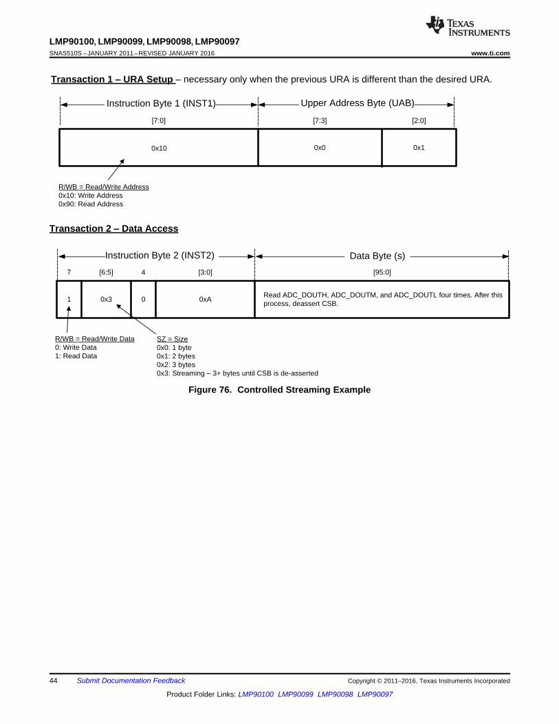
R/WB = Read/Write Data0: Write Data1: Read Data
7 [3:0] [95:0]
1 0x3
SZ = Size0x0: 1 byte0x1: 2 bytes0x2: 3 bytes0x3: Streaming ± 3+ bytes until CSB is de-asserted
[6:5] 4
0 0xARead ADC_DOUTH, ADC_DOUTM, and ADC_DOUTL four times. After this process, deassert CSB.
Instruction Byte 2 (INST2) Data Byte (s)
[7:0] [7:3] [2:0]
0x0 0x1
Instruction Byte 1 (INST1) Upper Address Byte (UAB)
R/WB = Read/Write Address0x10: Write Address0x90: Read Address
0x10
Transaction 2 ± Data Access
Transaction 1 ± URA Setup ± necessary only when the previous URA is different than the desired URA.
44
LMP90100, LMP90099, LMP90098, LMP90097SNAS510S –JANUARY 2011–REVISED JANUARY 2016 www.ti.com
Product Folder Links: LMP90100 LMP90099 LMP90098 LMP90097
Submit Documentation Feedback Copyright © 2011–2016, Texas Instruments Incorporated
Figure 76. Controlled Streaming Example

45
LMP90100, LMP90099, LMP90098, LMP90097www.ti.com SNAS510S –JANUARY 2011–REVISED JANUARY 2016
Product Folder Links: LMP90100 LMP90099 LMP90098 LMP90097
Submit Documentation FeedbackCopyright © 2011–2016, Texas Instruments Incorporated
9.6 Register Maps
Register Name ADDR(URA & LRA) Type Default
RESETCN Reset Control 0x00 WO -SPI_HANDSHAKECN SPI Handshake Control 0x01 R/W 0x00SPI_RESET SPI Reset Control 0x02 R/W 0x00SPI_STREAMCN SPI Stream Control 0x03 R/W 0x00Reserved - 0x04 - 0x07 - 0x00PWRCN Power Mode Control and Status 0x08 RO & WO 0x00DATA_ONLY_1 Data Only Read Control 1 0x09 R/W 0x1ADATA_ONLY_2 Data Only Read Control 2 0x0A R/W 0x02ADC_RESTART ADC Restart Conversion 0x0B WO -Reserved - 0x0C - 0x0D - 0x00GPIO_DIRCN GPIO Direction Control 0x0E R/W 0x00GPIO_DAT GPIO Data 0x0F RO & WO -BGCALCN Background Calibration Control 0x10 R/W 0x00SPI_DRDYBCN SPI Data Ready Bar Control 0x11 R/W 0x03ADC_AUXCN ADC Auxiliary Control 0x12 R/W 0x00SPI_CRC_CN CRC Control 0x13 R/W 0x02SENDIAG_THLD Sensor Diagnostic Threshold 1,0 0x14 - 0x15 R/W 0x0000Reserved - 0x16 - 0x00SCALCN System Calibration Control 0x17 R/W 0x00ADC_DONE ADC Data Available 0x18 RO -SENDIAG_FLAGS Sensor Diagnostic Flags 0x19 RO -ADC_DOUT Conversion Data 2,1,0 0x1A - 0x1C RO -SPI_CRC_DAT CRC Data 0x1D RO & WO -CHANNEL CONFIGURATION REGISTERS (CH4 to CH6 for LMP90100/LMP9099 only)CH_STS Channel Status 0x1E RO 0x00CH_SCAN Channel Scan Mode 0x1F R/W 0x30CH0_INPUTCN CH0 Input Control 0x20 R/W 0x01CH0_CONFIG CH0 Configuration 0x21 R/W 0x70CH1_INPUTCN CH1 Input Control 0X22 R/W 0x13CH1_CONFIG CH1 Configuration 0x23 R/W 0x70CH2_INPUTCN CH2 Input Control 0x24 R/W 0x25CH2_CONFIG CH2 Configuration 0x25 R/W 0x70CH3_INPUTCN CH3 Input Control 0x26 R/W 0x37CH3_CONFIG CH3 Configuration 0x27 R/W 0x70CH4_INPUTCN CH4 Input Control 0x28 R/W 0x01CH4_CONFIG CH4 Configuration 0x29 R/W 0x70CH5_INPUTCN CH5 Input Control 0x2A R/W 0x13CH5_CONFIG CH5 Configuration 0x2B R/W 0x70CH6_INPUTCN CH6 Input Control 0x2C R/W 0x25CH6_CONFIG CH6 Configuration 0x2D R/W 0x70Reserved - 0x2E - 0x2F - 0x00SYSTEM CALIBRATION REGISTERSCH0_SCAL_OFFSET CH0 System Calibration Offset Coefficients 0x30 - 0x32 R/W 0x00_0000CH0_SCAL_GAIN CH0 System Calibration Gain Coefficients 0x33 - 0x35 R/W 0x80_0000CH0_SCAL_SCALING CH0 System Calibration Scaling Coefficients 0x36 R/W 0x01

46
LMP90100, LMP90099, LMP90098, LMP90097SNAS510S –JANUARY 2011–REVISED JANUARY 2016 www.ti.com
Product Folder Links: LMP90100 LMP90099 LMP90098 LMP90097
Submit Documentation Feedback Copyright © 2011–2016, Texas Instruments Incorporated
Register Maps (continued)
Register Name ADDR(URA & LRA) Type Default
CH0_SCAL_BITS_SELECTOR CH0 System Calibration Bits Selector 0x37 R/W 0x00CH1_SCAL_OFFSET CH1 System Calibration Offset Coefficients 0x38 - 0x3A R/W 0x00_0000CH1_SCAL_GAIN CH1 System Calibration Gain Coefficient 0x3B - 0x3D R/W 0x80_0000CH1_SCAL_SCALING CH1 System Calibration Scaling Coefficients 0x3E R/W 0x01CH1_SCAL_BITS_SELECTOR CH1 System Calibration Bits Selector 0x3F R/W 0x00CH2_SCAL_OFFSET CH2 System Calibration Offset Coefficients 0x40 - 0x42 R/W 0x00_0000CH2_SCAL_GAIN CH2 System Calibration Gain Coefficient 0x43 - 0x45 R/W 0x80_0000CH2_SCAL_SCALING CH2 System Calibration Scaling Coefficients 0x46 R/W 0x01CH2_SCAL_BITS_SELECTOR CH2 System Calibration Bits Selector 0x47 R/W 0x00CH3_SCAL_OFFSET CH3 System Calibration Offset Coefficients 0x48 - 0x4A R/W 0x00_0000CH3_SCAL_GAIN CH3 System Calibration Gain Coefficient 0x4B - 0x4D R/W 0x80_0000CH3_SCAL_SCALING CH3 System Calibration Scaling Coefficients 0x4E R/W 0x01CH3_SCAL_BITS_SELECTOR CH3 System Calibration Bits Selector 0x4F R/W 0x00Reserved - 0x50 - 0x7F - 0x00
Table 7. RESETCN: Reset Control (Address 0x00)Bit Bit Symbol Bit Description
[7:0] REG_AND_CNV_ RSTRegister and Conversion Reset0xC3: Register and conversion resetOthers: Neglected
Table 8. SPI_HANDSHAKECN: SPI Handshake Control (Address 0x01)Bit Bit Symbol Bit Description
[7:4] Reserved -
[3:1] SDO_DRDYB_ DRIVER
SDO/DRDYB Driver – sets who is driving the SDO/DRYB pin
Whenever CSB isAsserted and the Deviceis Reading ADC_DOUT
Whenever CSB isAsserted and the Deviceis Not ReadingADC_DOUT
CSB is Deasserted
0x0 (default) SDO is driving DRDYB is driving High-Z0x3 SDO is driving DRDYB is driving DRDYB is driving0x4 SDO is driving High-Z High-ZOthers Forbidden
0 SW_OFF_TRG
Switch-off trigger - refers to the switching of the output drive from the slave to the master.0 (default): SDO will be high-Z after the last (16th, 24th, 32nd, etc) rising edge of SCLK. Thisoption allows time for the slave to transfer control back to the master at the end of the frame.
1: SDO’s high-Z is postponed to the subsequent falling edge following the last (16th, 24th, 32nd,etc) rising edge of SCLK. This option provides additional hold time for the last bit, DB0, in non-streaming read transfers.

47
LMP90100, LMP90099, LMP90098, LMP90097www.ti.com SNAS510S –JANUARY 2011–REVISED JANUARY 2016
Product Folder Links: LMP90100 LMP90099 LMP90098 LMP90097
Submit Documentation FeedbackCopyright © 2011–2016, Texas Instruments Incorporated
Table 9. SPI_RESET: SPI Reset Control (Address 0x02)Bit Bit Symbol Bit Description
[0] SPI_ RST
SPI Reset Enable0x0 (default): SPI Reset Disabled0x1: SPI Reset EnabledNote: Once Written, The contents of this register are sticky. That is, the content of this registercannot be changed with subsequent write. However, a Register reset clears the register as well asthe sticky status.
Table 10. SPI_STREAMCN: SPI Streaming Control (Address 0x03)Bit Bit Symbol Bit Description
7 STRM_TYPEStream type0 (default): Normal Streaming mode1: Controlled Streaming mode
[6:0] STRM_ RANGEStream range – selects Range for Controlled Streaming modeDefault: 0x00
Table 11. PWRCN: Power Mode Control and Status (Address 0x08)Bit Bit Symbol Bit Description
[7:2] Reserved -
[1:0] PWRCN
Power ControlWrite Only – power down mode control0x0: Active Mode0x1: Power-down Mode0x3: Stand-by Mode
Read Only – the present mode is:0x0 (default): Active Mode0x1: Power-down Mode0x3: Stand-by Mode
Table 12. DATA_ONLY_1: Data Only Read Control 1 (Address 0x09)Bit Bit Symbol Bit Description
7 Reserved -
[6:0] DATA_ONLY_ADRStart address for the Data Only Read TransactionDefault: 0x1APlease refer to the description of DT_ONLY_SZ in DATA_ONLY_2 register.
Table 13. DATA_ONLY_2: Data Only Read Control 2 (Address 0x0A)Bit Bit Symbol Bit Description
[7:3] Reserved -[2:0]
DATA_ONLY_SZNumber of bytes to be read out in Data Only mode. A value of 0x0 means read one byte and 0x7means read 8 bytes.Default: 0x2
Table 14. ADC_RESTART: ADC Restart Conversion (Address 0x0B)Bit Bit Symbol Bit Description
[7:1] Reserved -
0 RESTARTRestart conversion1: Restart conversion.
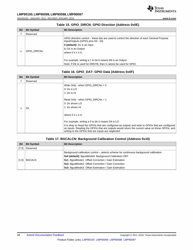
48
LMP90100, LMP90099, LMP90098, LMP90097SNAS510S –JANUARY 2011–REVISED JANUARY 2016 www.ti.com
Product Folder Links: LMP90100 LMP90099 LMP90098 LMP90097
Submit Documentation Feedback Copyright © 2011–2016, Texas Instruments Incorporated
Table 15. GPIO_DIRCN: GPIO Direction (Address 0x0E)Bit Bit Symbol Bit Description7 Reserved -
x GPIO_DIRCNx
GPIO direction control – these bits are used to control the direction of each General PurposeInput/Outputs (GPIO) pins D0 - D6.0 (default): Dx is an Input1: Dx is an Outputwhere 0 ≤ x ≤ 6.
For example, writing a 1 to bit 6 means D6 is an Output.Note: If D6 is used for DRDYB, then it cannot be used for GPIO.
Table 16. GPIO_DAT: GPIO Data (Address 0x0F)Bit Bit Symbol Bit Description7 Reserved -
x Dx
Write Only - when GPIO_DIRCNx = 00: Dx is LO1: Dx is HI
Read Only - when GPIO_DIRCNx = 10: Dx driven LO1: Dx driven HI
where 0 ≤ x ≤ 6.
For example, writing a 0 to bit 4 means D4 is LO.It is okay to Read the GPIOs that are configured as outputs and write to GPIOs that are configuredas inputs. Reading the GPIOs that are outputs would return the current value on those GPIOs, andwriting to the GPIOs that are inputs are neglected
Table 17. BGCALCN: Background Calibration Control (Address 0x10)Bit Bit Symbol Bit Description
[7:2] Reserved -
[1:0] BGCALN
Background calibration control – selects scheme for continuous background calibration.0x0 (default): BgcalMode0: Background Calibration OFF0x1: BgcalMode1: Offset Correction / Gain Estimation0x2: BgcalMode2: Offset Correction / Gain Correction0x3: BgcalMode3: Offset Estimation / Gain Estimation
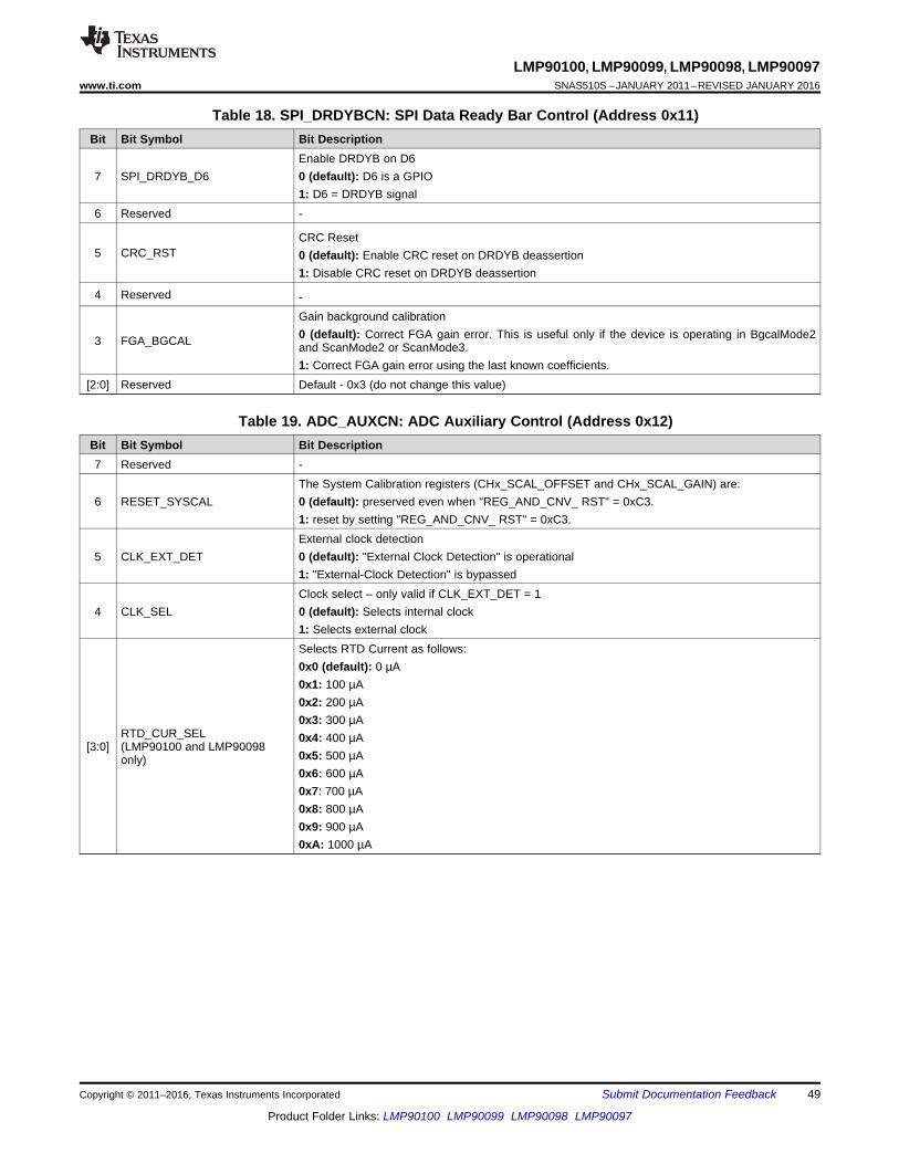
49
LMP90100, LMP90099, LMP90098, LMP90097www.ti.com SNAS510S –JANUARY 2011–REVISED JANUARY 2016
Product Folder Links: LMP90100 LMP90099 LMP90098 LMP90097
Submit Documentation FeedbackCopyright © 2011–2016, Texas Instruments Incorporated
Table 18. SPI_DRDYBCN: SPI Data Ready Bar Control (Address 0x11)Bit Bit Symbol Bit Description
7 SPI_DRDYB_D6Enable DRDYB on D60 (default): D6 is a GPIO1: D6 = DRDYB signal
6 Reserved -
5 CRC_RSTCRC Reset0 (default): Enable CRC reset on DRDYB deassertion1: Disable CRC reset on DRDYB deassertion
4 Reserved -
3 FGA_BGCAL
Gain background calibration0 (default): Correct FGA gain error. This is useful only if the device is operating in BgcalMode2and ScanMode2 or ScanMode3.1: Correct FGA gain error using the last known coefficients.
[2:0] Reserved Default - 0x3 (do not change this value)
Table 19. ADC_AUXCN: ADC Auxiliary Control (Address 0x12)Bit Bit Symbol Bit Description7 Reserved -
6 RESET_SYSCALThe System Calibration registers (CHx_SCAL_OFFSET and CHx_SCAL_GAIN) are:0 (default): preserved even when "REG_AND_CNV_ RST" = 0xC3.1: reset by setting "REG_AND_CNV_ RST" = 0xC3.
5 CLK_EXT_DETExternal clock detection0 (default): "External Clock Detection" is operational1: "External-Clock Detection" is bypassed
4 CLK_SELClock select – only valid if CLK_EXT_DET = 10 (default): Selects internal clock1: Selects external clock
[3:0]RTD_CUR_SEL(LMP90100 and LMP90098only)
Selects RTD Current as follows:0x0 (default): 0 µA0x1: 100 µA0x2: 200 µA0x3: 300 µA0x4: 400 µA0x5: 500 µA0x6: 600 µA0x7: 700 µA0x8: 800 µA0x9: 900 µA0xA: 1000 µA

50
LMP90100, LMP90099, LMP90098, LMP90097SNAS510S –JANUARY 2011–REVISED JANUARY 2016 www.ti.com
Product Folder Links: LMP90100 LMP90099 LMP90098 LMP90097
Submit Documentation Feedback Copyright © 2011–2016, Texas Instruments Incorporated
Table 20. SPI_CRC_CN: CRC Control (Address 0x13)Bit Bit Symbol Bit Description
[7:5] Reserved -
4 EN_CRCEnable CRC0 (default): Disable CRC1: Enable CRC
3 Reserved Default - 0x0 (do not change this value)
2 DRDYB_AFT_CRCDRDYB After CRC0 (default): DRDYB is deasserted (active high) after ADC_DOUTL is read.1: DRDYB is deasserted after SPI_CRC_DAT (which follows ADC_DOUTL), is read.
[1:0] Reserved -
Table 21. SENDIAG_THLD: Sensor Diagnostic Threshold (Address 0x14 to 0x15)Address Name Register Description
0x14 SENDIAG_THLDH Sensor Diagnostic threshold [15:8]0x15 SENDIAG_THLDL Sensor Diagnostic threshold [7:0]
Table 22. SCALCN: System Calibration Control (Address 0x17)Bit Bit Symbol Bit Description
[7:2] Reserved -
[1:0] SCALCN
System Calibration Control
When written, set SCALCN to:0x0 (default): Normal Mode0x1: “System Calibration Offset Coefficient Determination” mode0x2: “System Calibration Gain Coefficient Determination” mode0x3: Reserved
When read, this bit indicates the system calibration mode is in:0x0: Normal Mode0x1: "System Calibration Offset Coefficient Determination" mode0x2: "System Calibration Gain Coefficient Determination" mode0x3: ReservedNote: when read, this bit will indicate the current System Calibration status. Because thiscoefficient determination mode will only take 1 conversion cycle, reading this register will onlyreturn 0x00, unless this register is read within 1 conversion window.
Table 23. ADC_DONE: ADC Data Available (Address 0x18)Bit Bit Symbol Bit Description
[7:0] DT_AVAIL_BData Available – indicates if new conversion data is available0x00 − 0xFE: Available0xFF: Not available

51
LMP90100, LMP90099, LMP90098, LMP90097www.ti.com SNAS510S –JANUARY 2011–REVISED JANUARY 2016
Product Folder Links: LMP90100 LMP90099 LMP90098 LMP90097
Submit Documentation FeedbackCopyright © 2011–2016, Texas Instruments Incorporated
Table 24. SENDIAG_FLAGS: Sensor Diagnostic Flags (Address 0x19)Bit Bit Symbol Bit Description
7 SHORT_THLD_ FLAG Short Circuit Threshold Flag = 1 when the absolute value of VOUT is within the absolute thresholdvoltage set by SENDIAG_THLDH and SENDIAG_THLDL.
6 RAILS_FLAG Rails Flag = 1 when at least one of the inputs is near rail (VA or GND).
5 POR_AFT_LST_RD Power-on-reset after last read = 1 when there was a power-on-reset event because the last timethe SENDIAG_FLAGS register was read.
[4:3] OFLO_FLAGS
Overflow flags0x0: Normal operation0x1: The modulator was not overranged, but ADC_DOUT got clamped to 0x7f_ffff (positivefullscale) or 0x80_0000 (negative full scale)0x2: The modulator was over-ranged (VIN > 1.3*VREF/GAIN)0x3: The modulator was over-ranged (VIN < -1.3*VREF/GAIN)
[2:0] SAMPLED_CH Channel Number – the sampled channel for ADC_DOUT and SENDIAG_FLAGS.
Table 25. ADC_DOUT: 24-Bit Conversion Data (Two’s Complement) (Address 0x1A - 0x1C)Address Name Register Description
0x1A ADC_DOUTH ADC Conversion Data [23:16]0x1B ADC_DOUTM ADC Conversion Data [15:8]0x1C ADC_DOUTL ADC Conversion Data [7:0]
Note: Repeat reads of these registers are allowed as long as such reads are spaced apart by at least 72 µs.
Table 26. SPI_CRC_DAT: CRC Data (Address 0x1D)Bit Bit Symbol Bit Description
[7:0] CRC_DAT
CRC Data
When written, this register reset CRC:Any Value: Reset CRC
When read, this register indicates the CRC data.
Table 27. CH_STS: Channel Status (Address 0x1E)Bit Bit Symbol Bit Description
[7:2] Reserved -
1 CH_SCAN_NRDYChannel Scan Not Ready – indicates if it is okay to program CH_SCAN0: Update not pending, CH_SCAN register is okay to program1: Update pending, CH_SCAN register is not ready to be programmed
0 INV_OR_RPT_RD_STSInvalid or Repeated Read Status0: ADC_DOUT just read was valid and hitherto unread1: ADC_DOUT just read was either invalid (not ready) or there was a repeated read.
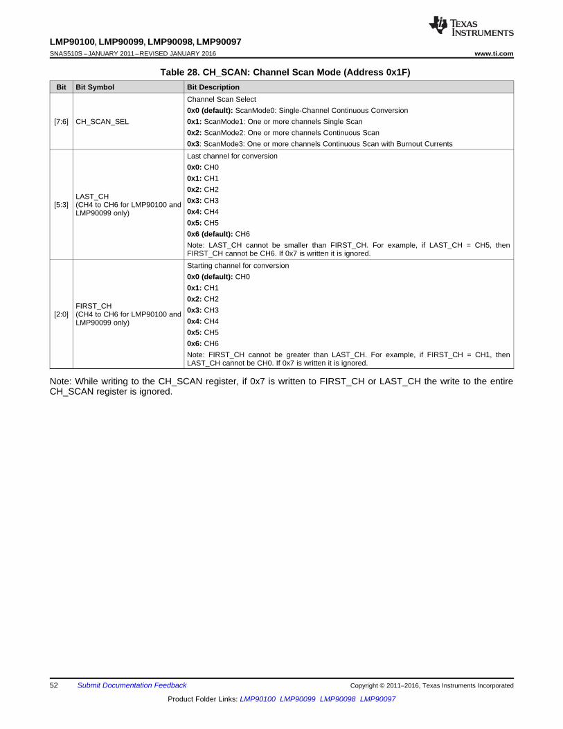
52
LMP90100, LMP90099, LMP90098, LMP90097SNAS510S –JANUARY 2011–REVISED JANUARY 2016 www.ti.com
Product Folder Links: LMP90100 LMP90099 LMP90098 LMP90097
Submit Documentation Feedback Copyright © 2011–2016, Texas Instruments Incorporated
Table 28. CH_SCAN: Channel Scan Mode (Address 0x1F)Bit Bit Symbol Bit Description
[7:6] CH_SCAN_SEL
Channel Scan Select0x0 (default): ScanMode0: Single-Channel Continuous Conversion0x1: ScanMode1: One or more channels Single Scan0x2: ScanMode2: One or more channels Continuous Scan0x3: ScanMode3: One or more channels Continuous Scan with Burnout Currents
[5:3]LAST_CH(CH4 to CH6 for LMP90100 andLMP90099 only)
Last channel for conversion0x0: CH00x1: CH10x2: CH20x3: CH30x4: CH40x5: CH50x6 (default): CH6Note: LAST_CH cannot be smaller than FIRST_CH. For example, if LAST_CH = CH5, thenFIRST_CH cannot be CH6. If 0x7 is written it is ignored.
[2:0]FIRST_CH(CH4 to CH6 for LMP90100 andLMP90099 only)
Starting channel for conversion0x0 (default): CH00x1: CH10x2: CH20x3: CH30x4: CH40x5: CH50x6: CH6Note: FIRST_CH cannot be greater than LAST_CH. For example, if FIRST_CH = CH1, thenLAST_CH cannot be CH0. If 0x7 is written it is ignored.
Note: While writing to the CH_SCAN register, if 0x7 is written to FIRST_CH or LAST_CH the write to the entireCH_SCAN register is ignored.
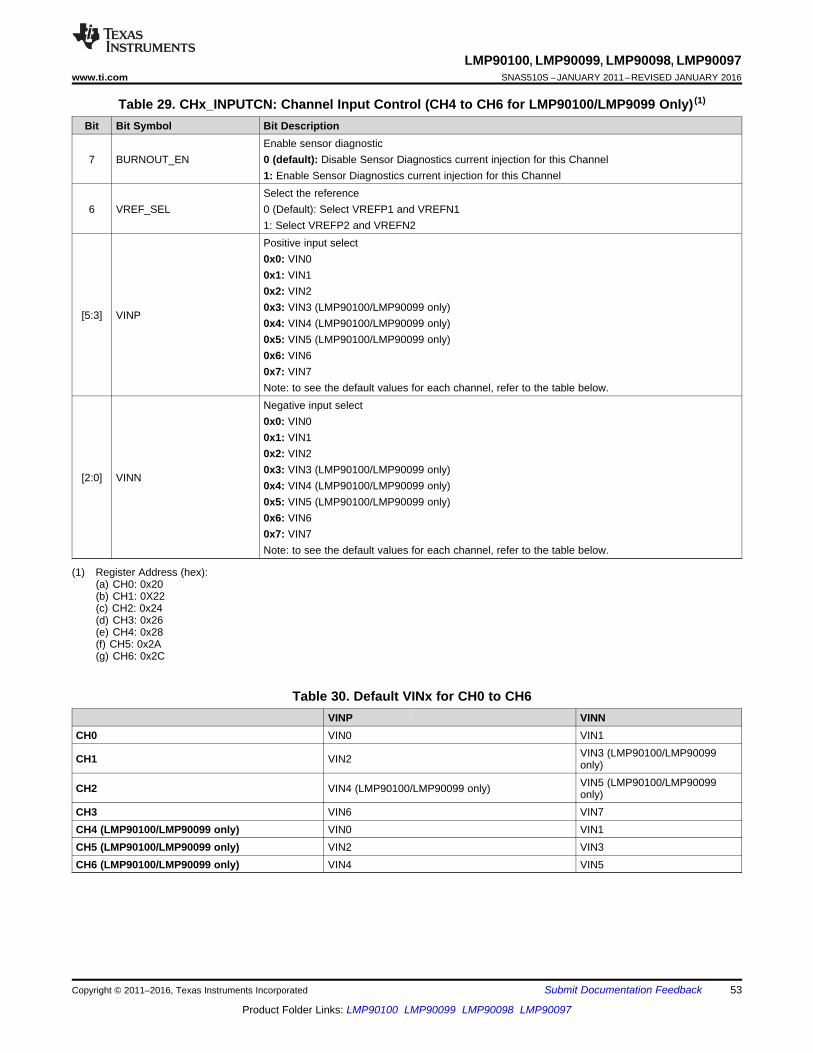
53
LMP90100, LMP90099, LMP90098, LMP90097www.ti.com SNAS510S –JANUARY 2011–REVISED JANUARY 2016
Product Folder Links: LMP90100 LMP90099 LMP90098 LMP90097
Submit Documentation FeedbackCopyright © 2011–2016, Texas Instruments Incorporated
(1) Register Address (hex):(a) CH0: 0x20(b) CH1: 0X22(c) CH2: 0x24(d) CH3: 0x26(e) CH4: 0x28(f) CH5: 0x2A(g) CH6: 0x2C
Table 29. CHx_INPUTCN: Channel Input Control (CH4 to CH6 for LMP90100/LMP9099 Only) (1)
Bit Bit Symbol Bit Description
7 BURNOUT_ENEnable sensor diagnostic0 (default): Disable Sensor Diagnostics current injection for this Channel1: Enable Sensor Diagnostics current injection for this Channel
6 VREF_SELSelect the reference0 (Default): Select VREFP1 and VREFN11: Select VREFP2 and VREFN2
[5:3] VINP
Positive input select0x0: VIN00x1: VIN10x2: VIN20x3: VIN3 (LMP90100/LMP90099 only)0x4: VIN4 (LMP90100/LMP90099 only)0x5: VIN5 (LMP90100/LMP90099 only)0x6: VIN60x7: VIN7Note: to see the default values for each channel, refer to the table below.
[2:0] VINN
Negative input select0x0: VIN00x1: VIN10x2: VIN20x3: VIN3 (LMP90100/LMP90099 only)0x4: VIN4 (LMP90100/LMP90099 only)0x5: VIN5 (LMP90100/LMP90099 only)0x6: VIN60x7: VIN7Note: to see the default values for each channel, refer to the table below.
Table 30. Default VINx for CH0 to CH6VINP VINN
CH0 VIN0 VIN1
CH1 VIN2 VIN3 (LMP90100/LMP90099only)
CH2 VIN4 (LMP90100/LMP90099 only) VIN5 (LMP90100/LMP90099only)
CH3 VIN6 VIN7CH4 (LMP90100/LMP90099 only) VIN0 VIN1CH5 (LMP90100/LMP90099 only) VIN2 VIN3CH6 (LMP90100/LMP90099 only) VIN4 VIN5

54
LMP90100, LMP90099, LMP90098, LMP90097SNAS510S –JANUARY 2011–REVISED JANUARY 2016 www.ti.com
Product Folder Links: LMP90100 LMP90099 LMP90098 LMP90097
Submit Documentation Feedback Copyright © 2011–2016, Texas Instruments Incorporated
(1) Register Address (hex):(a) CH0: 0x21(b) CH1: 0x23(c) CH2: 0x25(d) CH3: 0x27(e) CH4: 0x29(f) CH5: 0x2B(g) CH6: 0x2D
Table 31. CHx_CONFIG: Channel Configuration (CH4 to CH6 LMP90100/LMP90099 Only) (1)
Bit Bit Symbol Bit Description7 Reserved -
[6:4] ODR_SEL
ODR Select0x0: 13.42 / 8 = 1.6775 SPS0x1: 13.42 / 4 = 3.355 SPS0x2: 13.42 / 2 = 6.71 SPS0x3: 13.42 SPS0x4: 214.65 / 8 = 26.83125 SPS0x5: 214.65 / 4 = 53.6625 SPS0x6: 214.65 / 2 = 107.325 SPS0x7(default): 214.65 SPS
[3:1] GAIN_SEL
Gain Select0x0 (default): 1 (FGA OFF)0x1: 2 (FGA OFF)0x2: 4 (FGA OFF)0x3: 8 (FGA OFF)0x4: 16 (FGA ON)0x5: 32 (FGA ON)0x6: 64 (FGA ON)0x7: 128 (FGA ON)
0 BUF_EN
Enable/Disable the buffer0 (default): Exclude the buffer in the signal path1: Include the buffer from the signal pathNote: When gain ≥ 16, the buffer is automatically included in the signal path irrespective of this bit.
Table 32. CHX_SCAL_OFFSET: CH0 to CH3 System Calibration Offset Registers (Two's Complement)ADDR
NAME DESCRIPTIONCH0 CH1 CH2 CH30x30 0x38 0x40 0x48 CHx_SCAL_OFFSETH System Calibration Offset Coefficient Data [23:16]0x31 0x39 0x41 0x49 CHx_SCAL_OFFSETM System Calibration Offset Coefficient Data [15:8]0x32 0x3A 0x42 0x4A CHx_SCAL_OFFSETL System Calibration Offset Coefficient Data[7:0]
Table 33. CHX_SCAL_GAIN: CH0 to CH3 System Calibration Gain Registers (Fixed Point 1.23 Format)ADDR
NAME DESCRIPTIONCH0 CH1 CH2 CH30x33 0x3B 0x43 0x4B CHx_SCAL_GAINH System Calibration Gain Coefficient Data [23:16]0x34 0x3C 0x44 0x4C CHx_SCAL_GAINM System Calibration Gain Coefficient Data [15:8]0x35 0x3D 0x45 0x4D CHx_SCAL_GAINL System Calibration Gain Coefficient Data[7:0]
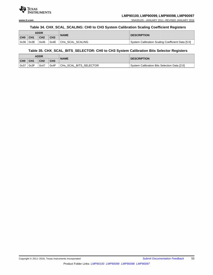
55
LMP90100, LMP90099, LMP90098, LMP90097www.ti.com SNAS510S –JANUARY 2011–REVISED JANUARY 2016
Product Folder Links: LMP90100 LMP90099 LMP90098 LMP90097
Submit Documentation FeedbackCopyright © 2011–2016, Texas Instruments Incorporated
Table 34. CHX_SCAL_SCALING: CH0 to CH3 System Calibration Scaling Coefficient RegistersADDR
NAME DESCRIPTIONCH0 CH1 CH2 CH30x36 0x3E 0x46 0x4E CHx_SCAL_SCALING System Calibration Scaling Coefficient Data [5:0]
Table 35. CHX_SCAL_BITS_SELECTOR: CH0 to CH3 System Calibration Bits Selector RegistersADDR
NAME DESCRIPTIONCH0 CH1 CH2 CH30x37 0x3F 0x47 0x4F CHx_SCAL_BITS_SELECTOR System Calibration Bits Selection Data [2:0]

ADC_DOUT ¨©
§= ¸
¹
· ( )232x±
GAIN(VINP - VINN) x
VREFP - VREFN
56
LMP90100, LMP90099, LMP90098, LMP90097SNAS510S –JANUARY 2011–REVISED JANUARY 2016 www.ti.com
Product Folder Links: LMP90100 LMP90099 LMP90098 LMP90097
Submit Documentation Feedback Copyright © 2011–2016, Texas Instruments Incorporated
10 Application and Implementation
NOTEInformation in the following applications sections is not part of the TI componentspecification, and TI does not warrant its accuracy or completeness. TI’s customers areresponsible for determining suitability of components for their purposes. Customers shouldvalidate and test their design implementation to confirm system functionality.
10.1 Application InformationThe LMP90100/LMP90099/LMP90098/LMP90097 are highly integrated, multi-channel, low power 24-bit SensorAFEs. The devices features a precision, 24-bit Sigma Delta Analog-to-Digital Converter (ADC) with a low-noiseprogrammable gain amplifier and a fully differential high impedance analog input multiplexer. A true continuousbackground calibration feature allows calibration at all gains and output data rates without interrupting the signalpath. The background calibration feature essentially eliminates gain and offset errors across temperature andtime, providing measurement accuracy without sacrificing speed and power consumption.
10.1.1 Quick StartThis section shows step-by-step instructions to configure the LMP90xxx to perform a simple DC reading fromCH0.1. Apply VA = VIO = VREFP1 = 5V, and ground VREFN12. Apply VINP = ¾VREF and VINN = ¼VREF for CH0. Thus, set CH0 = VIN = VINP - VINN = ½VREF
(CH0_INPUTCN register)3. Set gain = 1 (CH0_CONFIG: GAIN_SEL = 0x0)4. Exclude the buffer from the signal path (CH0_CONFIG: BUF_EN = 0)5. Set the background to BgcalMode2 (BGCALCN = 0x2)6. Select VREF1 (CH0_INPUTCN: VREF_SEL = 0)7. To use the internal CLK, set CLK_EXT_DET = 1 and CLK_SEL = 0.8. Follow the register read/write protocol (Figure 60) to capture ADC_DOUT from CH0.
10.1.2 ADC_DOUT CalculationThe output code of the LMP90xxx can be calculated as:
Equation 1 — Output Code (13)
ADC_DOUT is in 24−bit two's complement binary format. The largest positive value is 0x7F_FFFF while thelargest negative value is 0x80_0000. In case of an over range the value is automatically clamped to one of thesetwo values.
Figure 77 shows the theoretical output code, ADC_DOUT, vs. analog input voltage, VIN, using the equationabove.
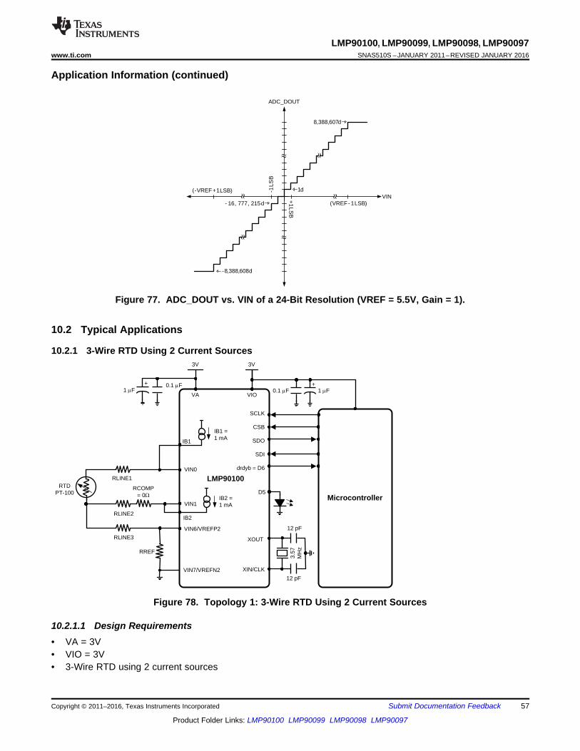
RLINE1
RLINE2
RREF
IB1
VIN7/VREFN2
IB2
RLINE3
VIN6/VREFP2
VIN0
VIN1
VA
RTDPT-100
RCOMP = 0:
IB1 = 1 mA
IB2 = 1 mA
+ 0.1 PF +
VIO
LMP90100
XOUT
XIN/CLK
SCLK
CSB
SDO
SDI
drdyb = D6
Microcontroller
3V 3V
12 pF
12 pF
D5
3.57
M
Hz
1 PF 0.1 PF 1 PF
|
- 8,388,608d
1d
ADC_DOUT
- 16, 777, 215d
|
|
VIN
8,388,607d
|
|
-1 LS
B
(VREF - 1LSB)
+1
LSB
|
(-VREF + 1LSB)
57
LMP90100, LMP90099, LMP90098, LMP90097www.ti.com SNAS510S –JANUARY 2011–REVISED JANUARY 2016
Product Folder Links: LMP90100 LMP90099 LMP90098 LMP90097
Submit Documentation FeedbackCopyright © 2011–2016, Texas Instruments Incorporated
Application Information (continued)
Figure 77. ADC_DOUT vs. VIN of a 24-Bit Resolution (VREF = 5.5V, Gain = 1).
10.2 Typical Applications
10.2.1 3-Wire RTD Using 2 Current Sources
Figure 78. Topology 1: 3-Wire RTD Using 2 Current Sources
10.2.1.1 Design Requirements• VA = 3V• VIO = 3V• 3-Wire RTD using 2 current sources
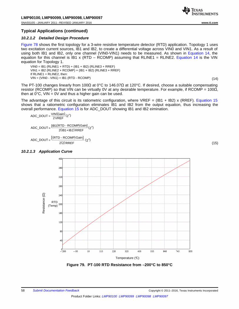
Res
ista
nce
( )
RTD (Temp)
Temperature (°C)
=)([IB1
( )n2( )RREFIBIB 212 +
( )nADC_DOUT 2=
2VREF
( )GainVIN
=( )22
(> @)GainRTD - RCOMP( )n2
ADC_DOUT
ADC_DOUT
RTD - RCOMP Gain]
RREF
VIN0 = IB1 (RLINE1 + RTD) + (IB1 + IB2) (RLINE3 + RREF)VIN1 = IB2 (RLINE2 + RCOMP) + (IB1 + IB2) (RLINE3 + RREF)If RLINE1 = RLINE2, then:VIN = (VIN0 - VIN1) = IB1 (RTD - RCOMP)
58
LMP90100, LMP90099, LMP90098, LMP90097SNAS510S –JANUARY 2011–REVISED JANUARY 2016 www.ti.com
Product Folder Links: LMP90100 LMP90099 LMP90098 LMP90097
Submit Documentation Feedback Copyright © 2011–2016, Texas Instruments Incorporated
Typical Applications (continued)10.2.1.2 Detailed Design ProcedureFigure 78 shows the first topology for a 3-wire resistive temperature detector (RTD) application. Topology 1 usestwo excitation current sources, IB1 and IB2, to create a differential voltage across VIN0 and VIN1. As a result ofusing both IB1 and IB2, only one channel (VIN0-VIN1) needs to be measured. As shown in Equation 14, theequation for this channel is IB1 x (RTD – RCOMP) assuming that RLINE1 = RLINE2. Equation 14 is the VINequation for Topology 1.
(14)
The PT-100 changes linearly from 100Ω at 0°C to 146.07Ω at 120°C. If desired, choose a suitable compensatingresistor (RCOMP) so that VIN can be virtually 0V at any desirable temperature. For example, if RCOMP = 100Ω,then at 0°C, VIN = 0V and thus a higher gain can be used.
The advantage of this circuit is its ratiometric configuration, where VREF = (IB1 + IB2) x (RREF). Equation 15shows that a ratiometric configuration eliminates IB1 and IB2 from the output equation, thus increasing theoverall performance. Equation 15 is for ADC_DOUT showing IB1 and IB2 eimination.
(15)
10.2.1.3 Application Curve
Figure 79. PT-100 RTD Resistance from –200°C to 850°C
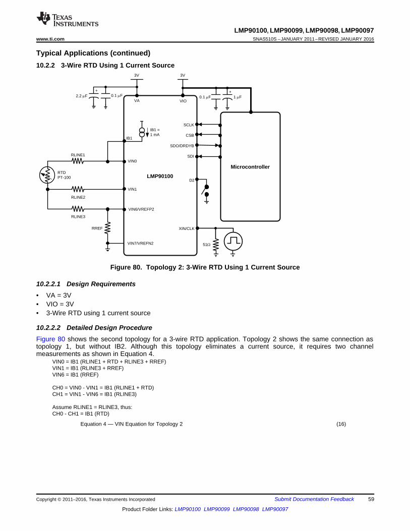
VIN0 = IB1 (RLINE1 + RTD + RLINE3 + RREF)VIN1 = IB1 (RLINE3 + RREF)VIN6 = IB1 (RREF)
CH0 = VIN0 - VIN1 = IB1 (RLINE1 + RTD)CH1 = VIN1 - VIN6 = IB1 (RLINE3)
Assume RLINE1 = RLINE3, thus:CH0 - CH1 = IB1 (RTD)
RLINE1
RLINE2
RREF
IB1
VIN7/VREFN2
RLINE3
VIN6/VREFP2
VIN0
VIN1
VA
RTDPT-100
IB1 = 1 mA
+2.2 PF 0.1 PF
+1 PF0.1 PF
VIO
LMP90100
XIN/CLK
SCLK
CSB
SDO/DRDYB
SDI
Microcontroller
3V 3V
D2
OSC
51:
59
LMP90100, LMP90099, LMP90098, LMP90097www.ti.com SNAS510S –JANUARY 2011–REVISED JANUARY 2016
Product Folder Links: LMP90100 LMP90099 LMP90098 LMP90097
Submit Documentation FeedbackCopyright © 2011–2016, Texas Instruments Incorporated
Typical Applications (continued)10.2.2 3-Wire RTD Using 1 Current Source
Figure 80. Topology 2: 3-Wire RTD Using 1 Current Source
10.2.2.1 Design Requirements• VA = 3V• VIO = 3V• 3-Wire RTD using 1 current source
10.2.2.2 Detailed Design ProcedureFigure 80 shows the second topology for a 3-wire RTD application. Topology 2 shows the same connection astopology 1, but without IB2. Although this topology eliminates a current source, it requires two channelmeasurements as shown in Equation 4.
Equation 4 — VIN Equation for Topology 2 (16)

Res
ista
nce
( )
RTD (Temp)
Temperature (°C)
60
LMP90100, LMP90099, LMP90098, LMP90097SNAS510S –JANUARY 2011–REVISED JANUARY 2016 www.ti.com
Product Folder Links: LMP90100 LMP90099 LMP90098 LMP90097
Submit Documentation Feedback Copyright © 2011–2016, Texas Instruments Incorporated
Typical Applications (continued)10.2.2.3 Application Curve
Figure 81. PT-100 RTD Resistance from –200°C to 850°C

VREFN1
VREFP1
VIN4
VIN3
VA
+
1 PF 0.1 PF+
1 PF0.1 PFVIO
LMP90100
XOUT
XIN/CLK
SCLK
CSB
SDO
SDI
D6 = DRDYB
Microcontroller
5V 2.7V
LM94022IC Temp Sensor
Thot
Tcold
+TC [ VIN4 ± VIN3]-
TcoldVIN5
VREFP1
Thermocouple
2k
2k
2.2 PF
10 nF
10 nF
LM4140-4.1
+0.1 PF
0.1 PF+
1 PF 0.1 PF
5V
5V
VIN7
+LM [ VIN5]-
GND
1 PF
61
LMP90100, LMP90099, LMP90098, LMP90097www.ti.com SNAS510S –JANUARY 2011–REVISED JANUARY 2016
Product Folder Links: LMP90100 LMP90099 LMP90098 LMP90097
Submit Documentation FeedbackCopyright © 2011–2016, Texas Instruments Incorporated
Typical Applications (continued)10.2.3 Thermocouple with Cold Junction Compensation
Figure 82. Thermocouple With CJC
10.2.3.1 Design Requirements• VA = 5V• VIO = 2.7V• Thermocouple with Cold Junction Compensation
10.2.3.2 Detailed Design ProcedureThe LMP90xxx is also ideal for thermocouple temperature applications. Thermocouples have several advantagesthat make them popular in many industrial and medical applications. Compare to RTDs, thermistors, and ICsensors, thermocouples are the most rugged, least expensive, and can operate over the largest temperaturerange.
A thermocouple is a sensor whose junction generates a differential voltage, VIN, that is relative to thetemperature difference (Thot – Tcold). Thot is also known as the measuring junction or “hot” junction, which isplaced at the measured environment. Tcold is also known as the reference or “cold” junction, which is placed atthe measuring system environment.
Because a thermocouple can only measure a temperature difference, it does not have the ability to measureabsolute temperature. To determine the absolute temperature of the measured environment (Thot), a techniqueknown as cold junction compensation (CJC) must be used.
In a CJC technique, the “cold” junction temperature, Tcold, is sensed by using an IC temperature sensor, suchas the LM94022. The temperature sensor should be placed within close proximity of the reference junction andshould have an isothermal connection to the board to minimize any potential temperature gradients.
Once Tcold is obtained, use a standard thermocouple look-up-table to find its equivalent voltage. Next, measurethe differential thermocouple voltage and add the equivalent cold junction voltage. Lastly, convert the resultingvoltage to temperature using a standard thermocouple look-up-table.

62
LMP90100, LMP90099, LMP90098, LMP90097SNAS510S –JANUARY 2011–REVISED JANUARY 2016 www.ti.com
Product Folder Links: LMP90100 LMP90099 LMP90098 LMP90097
Submit Documentation Feedback Copyright © 2011–2016, Texas Instruments Incorporated
Typical Applications (continued)For example, assume Tcold = 20°C. The equivalent voltage from a type K thermocouple look-up-table is 0.798mV. Next, add the measured differential thermocouple voltage to the Tcold equivalent voltage. For example, ifthe thermocouple voltage is 4.096 mV, the total would be 0.798 mV + 4.096 mV = 4.894 mV. Referring to thetype K thermocouple table gives a temperature of 119.37°C for 4.894 mV.
10.2.4 Application Curve
Figure 83. Thermocouple Output as Function of Temperature

63
LMP90100, LMP90099, LMP90098, LMP90097www.ti.com SNAS510S –JANUARY 2011–REVISED JANUARY 2016
Product Folder Links: LMP90100 LMP90099 LMP90098 LMP90097
Submit Documentation FeedbackCopyright © 2011–2016, Texas Instruments Incorporated
11 Power Supply Recommendations
11.1 VA and VIOAny ADC architecture is sensitive to spikes on the analog voltage, VA, digital input/output voltage, VIO, andground pins. These spikes may originate from switching power supplies, digital logic, high power devices, andother sources. To diminish these spikes, the LMP90xxx’s VA and VIO pins should be clean and well bypassed. A0.1 µF ceramic bypass capacitor and a 1 µF tantalum capacitor should be used to bypass the LMP90xxxsupplies, with the 0.1 µF capacitor placed as close to the LMP90xxx as possible.
Because the LMP90xxx has both external VA and VIO pins, the user has two options on how to connect thesepins. The first option is to tie VA and VIO together and power them with the same power supply. This is the mostcost effective way of powering the LMP90xxx but is also the least ideal because noise from VIO can couple intoVA and negatively affect performance. The second option involves powering VA and VIO with separate powersupplies. These supply voltages can have the same amplitude or they can be different.
11.2 VREFOperation with VREF below VA is also possible with slightly diminished performance. As VREF is reduced, therange of acceptable analog input voltages is also reduced. Reducing the value of VREF also reduces the size ofthe LSB. When the LSB size goes below the noise floor of the LMP90xxx, the noise will span an increasingnumber of codes and performance will degrade. For optimal performance, VREF should be the same as VA andsourced with a clean source that is bypassed with a ceramic capacitor value of 0.1 µF and a tantalum capacitorof 10 µF.
LMP90xxx also allows ratiometric connection for noise immunity reasons. A ratiometric connection is when theADC’s VREFP and VREFN are used to excite the input device’s (i.e. a bridge sensor) voltage references. Thistype of connection severely attenuates any VREF ripple seen the ADC output, and is thus stronglyrecommended.
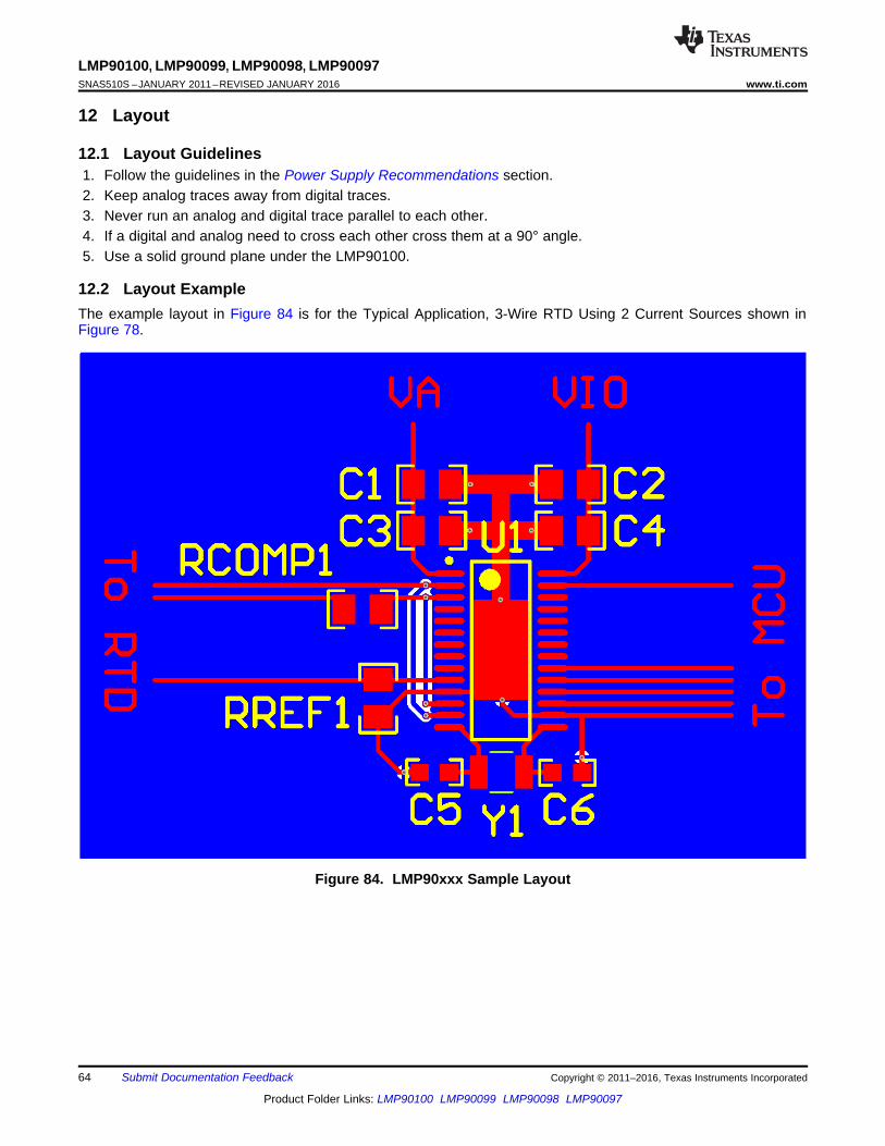
64
LMP90100, LMP90099, LMP90098, LMP90097SNAS510S –JANUARY 2011–REVISED JANUARY 2016 www.ti.com
Product Folder Links: LMP90100 LMP90099 LMP90098 LMP90097
Submit Documentation Feedback Copyright © 2011–2016, Texas Instruments Incorporated
12 Layout
12.1 Layout Guidelines1. Follow the guidelines in the Power Supply Recommendations section.2. Keep analog traces away from digital traces.3. Never run an analog and digital trace parallel to each other.4. If a digital and analog need to cross each other cross them at a 90° angle.5. Use a solid ground plane under the LMP90100.
12.2 Layout ExampleThe example layout in Figure 84 is for the Typical Application, 3-Wire RTD Using 2 Current Sources shown inFigure 78.
Figure 84. LMP90xxx Sample Layout

NFR = ¸̧¹
·¨̈©
§
Peak-to-Peak Noise2 x VREF/Gainlog2
ENOB = ¸̧¹
·¨̈©
§
RMS Noise2 x VREF/Gainlog2
65
LMP90100, LMP90099, LMP90098, LMP90097www.ti.com SNAS510S –JANUARY 2011–REVISED JANUARY 2016
Product Folder Links: LMP90100 LMP90099 LMP90098 LMP90097
Submit Documentation FeedbackCopyright © 2011–2016, Texas Instruments Incorporated
13 Device and Documentation Support
13.1 Device Support
13.1.1 Device Nomenclature
13.1.1.1 Specific DefinitionsCMRR = 20 LOG(ΔCommon Input / ΔOutput Offset)
COMMON MODE REJECTION RATIO is a measure of how well in-phase signals common to both input pins arerejected. To calculate CMRR, the change in output offset is measured while the common modeinput voltage is changed.
EFFECTIVE NUMBER OF BITS (ENOB, or EFFECTIVE BITS) – says that the converter is equivalent to aperfect ADC of this (ENOB) number of bits. LMP90xxx’s ENOB is a DC ENOB spec, not thedynamic ENOB that is measured using FFT and SINAD. Its equation is as follows:
(17)
GAIN ERROR is the deviation from the ideal slope of the transfer function.
INTEGRAL NON-LINEARITY (INL) is a measure of the deviation of each individual code from a straight linethrough the input to output transfer function. The deviation of any given code from this straight lineis measured from the center of that code value. The end point fit method is used. INL for thisproduct is specified over a limited range, per the Electrical Tables.
NEGATIVE FULL-SCALE ERROR is the difference between the differential input voltage at which the outputcode transitions to negative full scale and (-VREF + 1LSB).
NEGATIVE GAIN ERROR is the difference between the negative full-scale error and the offset error divided by(VREF / Gain).
NOISE FREE RESOLUTION is a method of specifying the number of bits for a converter with noise.
(18)
ODR Output Data Rate.
OFFSET ERROR is the difference between the differential input voltage at which the output code transitionsfrom code 0000h to 0001h and 1 LSB.
POSITIVE FULL-SCALE ERROR is the difference between the differential input voltage at which the outputcode transitions to positive full scale and (VREF – 1LSB).
POSITIVE GAIN ERROR is the difference between the positive full-scale error and the offset error divided by(VREF / Gain).
POWER SUPPLY REJECTION RATIO (PSRR) is a measure of how well a change in the analog supply voltageis rejected. PSRR is calculated from the ratio of the change in offset error for a given change insupply voltage, expressed in dB.
PSRR = 20 LOG (ΔVA / ΔOutput Offset)

66
LMP90100, LMP90099, LMP90098, LMP90097SNAS510S –JANUARY 2011–REVISED JANUARY 2016 www.ti.com
Product Folder Links: LMP90100 LMP90099 LMP90098 LMP90097
Submit Documentation Feedback Copyright © 2011–2016, Texas Instruments Incorporated
13.2 Related LinksThe table below lists quick access links. Categories include technical documents, support and communityresources, tools and software, and quick access to sample or buy.
Table 36. Related Links
PARTS PRODUCT FOLDER SAMPLE & BUY TECHNICALDOCUMENTS
TOOLS &SOFTWARE
SUPPORT &COMMUNITY
LMP90100 Click here Click here Click here Click here Click hereLMP90099 Click here Click here Click here Click here Click hereLMP90098 Click here Click here Click here Click here Click hereLMP90097 Click here Click here Click here Click here Click here
13.3 Community ResourcesThe following links connect to TI community resources. Linked contents are provided "AS IS" by the respectivecontributors. They do not constitute TI specifications and do not necessarily reflect TI's views; see TI's Terms ofUse.
TI E2E™ Online Community TI's Engineer-to-Engineer (E2E) Community. Created to foster collaborationamong engineers. At e2e.ti.com, you can ask questions, share knowledge, explore ideas and helpsolve problems with fellow engineers.
Design Support TI's Design Support Quickly find helpful E2E forums along with design support tools andcontact information for technical support.
13.4 TrademarksE2E is a trademark of Texas Instruments.WEBENCH is a registered trademark of Texas Instruments.All other trademarks are the property of their respective owners.
13.5 Electrostatic Discharge CautionThese devices have limited built-in ESD protection. The leads should be shorted together or the device placed in conductive foamduring storage or handling to prevent electrostatic damage to the MOS gates.
13.6 GlossarySLYZ022 — TI Glossary.
This glossary lists and explains terms, acronyms, and definitions.
14 Mechanical, Packaging, and Orderable InformationThe following pages include mechanical packaging and orderable information. This information is the mostcurrent data available for the designated devices. This data is subject to change without notice and revision ofthis document. For browser-based versions of this data sheet, refer to the left-hand navigation.
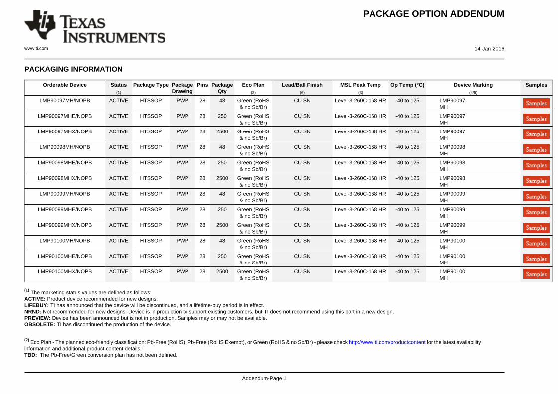
PACKAGE OPTION ADDENDUM
www.ti.com 14-Jan-2016
Addendum-Page 1
PACKAGING INFORMATION
Orderable Device Status(1)
Package Type PackageDrawing
Pins PackageQty
Eco Plan(2)
Lead/Ball Finish(6)
MSL Peak Temp(3)
Op Temp (°C) Device Marking(4/5)
Samples
LMP90097MH/NOPB ACTIVE HTSSOP PWP 28 48 Green (RoHS& no Sb/Br)
CU SN Level-3-260C-168 HR -40 to 125 LMP90097MH
LMP90097MHE/NOPB ACTIVE HTSSOP PWP 28 250 Green (RoHS& no Sb/Br)
CU SN Level-3-260C-168 HR -40 to 125 LMP90097MH
LMP90097MHX/NOPB ACTIVE HTSSOP PWP 28 2500 Green (RoHS& no Sb/Br)
CU SN Level-3-260C-168 HR -40 to 125 LMP90097MH
LMP90098MH/NOPB ACTIVE HTSSOP PWP 28 48 Green (RoHS& no Sb/Br)
CU SN Level-3-260C-168 HR -40 to 125 LMP90098MH
LMP90098MHE/NOPB ACTIVE HTSSOP PWP 28 250 Green (RoHS& no Sb/Br)
CU SN Level-3-260C-168 HR -40 to 125 LMP90098MH
LMP90098MHX/NOPB ACTIVE HTSSOP PWP 28 2500 Green (RoHS& no Sb/Br)
CU SN Level-3-260C-168 HR -40 to 125 LMP90098MH
LMP90099MH/NOPB ACTIVE HTSSOP PWP 28 48 Green (RoHS& no Sb/Br)
CU SN Level-3-260C-168 HR -40 to 125 LMP90099MH
LMP90099MHE/NOPB ACTIVE HTSSOP PWP 28 250 Green (RoHS& no Sb/Br)
CU SN Level-3-260C-168 HR -40 to 125 LMP90099MH
LMP90099MHX/NOPB ACTIVE HTSSOP PWP 28 2500 Green (RoHS& no Sb/Br)
CU SN Level-3-260C-168 HR -40 to 125 LMP90099MH
LMP90100MH/NOPB ACTIVE HTSSOP PWP 28 48 Green (RoHS& no Sb/Br)
CU SN Level-3-260C-168 HR -40 to 125 LMP90100MH
LMP90100MHE/NOPB ACTIVE HTSSOP PWP 28 250 Green (RoHS& no Sb/Br)
CU SN Level-3-260C-168 HR -40 to 125 LMP90100MH
LMP90100MHX/NOPB ACTIVE HTSSOP PWP 28 2500 Green (RoHS& no Sb/Br)
CU SN Level-3-260C-168 HR -40 to 125 LMP90100MH
(1) The marketing status values are defined as follows:ACTIVE: Product device recommended for new designs.LIFEBUY: TI has announced that the device will be discontinued, and a lifetime-buy period is in effect.NRND: Not recommended for new designs. Device is in production to support existing customers, but TI does not recommend using this part in a new design.PREVIEW: Device has been announced but is not in production. Samples may or may not be available.OBSOLETE: TI has discontinued the production of the device.
(2) Eco Plan - The planned eco-friendly classification: Pb-Free (RoHS), Pb-Free (RoHS Exempt), or Green (RoHS & no Sb/Br) - please check http://www.ti.com/productcontent for the latest availabilityinformation and additional product content details.TBD: The Pb-Free/Green conversion plan has not been defined.

PACKAGE OPTION ADDENDUM
www.ti.com 14-Jan-2016
Addendum-Page 2
Pb-Free (RoHS): TI's terms "Lead-Free" or "Pb-Free" mean semiconductor products that are compatible with the current RoHS requirements for all 6 substances, including the requirement thatlead not exceed 0.1% by weight in homogeneous materials. Where designed to be soldered at high temperatures, TI Pb-Free products are suitable for use in specified lead-free processes.Pb-Free (RoHS Exempt): This component has a RoHS exemption for either 1) lead-based flip-chip solder bumps used between the die and package, or 2) lead-based die adhesive used betweenthe die and leadframe. The component is otherwise considered Pb-Free (RoHS compatible) as defined above.Green (RoHS & no Sb/Br): TI defines "Green" to mean Pb-Free (RoHS compatible), and free of Bromine (Br) and Antimony (Sb) based flame retardants (Br or Sb do not exceed 0.1% by weightin homogeneous material)
(3) MSL, Peak Temp. - The Moisture Sensitivity Level rating according to the JEDEC industry standard classifications, and peak solder temperature.
(4) There may be additional marking, which relates to the logo, the lot trace code information, or the environmental category on the device.
(5) Multiple Device Markings will be inside parentheses. Only one Device Marking contained in parentheses and separated by a "~" will appear on a device. If a line is indented then it is a continuationof the previous line and the two combined represent the entire Device Marking for that device.
(6) Lead/Ball Finish - Orderable Devices may have multiple material finish options. Finish options are separated by a vertical ruled line. Lead/Ball Finish values may wrap to two lines if the finishvalue exceeds the maximum column width.
Important Information and Disclaimer:The information provided on this page represents TI's knowledge and belief as of the date that it is provided. TI bases its knowledge and belief on informationprovided by third parties, and makes no representation or warranty as to the accuracy of such information. Efforts are underway to better integrate information from third parties. TI has taken andcontinues to take reasonable steps to provide representative and accurate information but may not have conducted destructive testing or chemical analysis on incoming materials and chemicals.TI and TI suppliers consider certain information to be proprietary, and thus CAS numbers and other limited information may not be available for release.
In no event shall TI's liability arising out of such information exceed the total purchase price of the TI part(s) at issue in this document sold by TI to Customer on an annual basis.

TAPE AND REEL INFORMATION
*All dimensions are nominal
Device PackageType
PackageDrawing
Pins SPQ ReelDiameter
(mm)
ReelWidth
W1 (mm)
A0(mm)
B0(mm)
K0(mm)
P1(mm)
W(mm)
Pin1Quadrant
LMP90097MHE/NOPB HTSSOP PWP 28 250 178.0 16.4 6.8 10.2 1.6 8.0 16.0 Q1
LMP90097MHX/NOPB HTSSOP PWP 28 2500 330.0 16.4 6.8 10.2 1.6 8.0 16.0 Q1
LMP90098MHE/NOPB HTSSOP PWP 28 250 178.0 16.4 6.8 10.2 1.6 8.0 16.0 Q1
LMP90098MHX/NOPB HTSSOP PWP 28 2500 330.0 16.4 6.8 10.2 1.6 8.0 16.0 Q1
LMP90099MHE/NOPB HTSSOP PWP 28 250 178.0 16.4 6.8 10.2 1.6 8.0 16.0 Q1
LMP90099MHX/NOPB HTSSOP PWP 28 2500 330.0 16.4 6.8 10.2 1.6 8.0 16.0 Q1
LMP90100MHE/NOPB HTSSOP PWP 28 250 178.0 16.4 6.8 10.2 1.6 8.0 16.0 Q1
LMP90100MHX/NOPB HTSSOP PWP 28 2500 330.0 16.4 6.8 10.2 1.6 8.0 16.0 Q1
PACKAGE MATERIALS INFORMATION
www.ti.com 20-Sep-2016
Pack Materials-Page 1

*All dimensions are nominal
Device Package Type Package Drawing Pins SPQ Length (mm) Width (mm) Height (mm)
LMP90097MHE/NOPB HTSSOP PWP 28 250 210.0 185.0 35.0
LMP90097MHX/NOPB HTSSOP PWP 28 2500 367.0 367.0 38.0
LMP90098MHE/NOPB HTSSOP PWP 28 250 210.0 185.0 35.0
LMP90098MHX/NOPB HTSSOP PWP 28 2500 367.0 367.0 38.0
LMP90099MHE/NOPB HTSSOP PWP 28 250 210.0 185.0 35.0
LMP90099MHX/NOPB HTSSOP PWP 28 2500 367.0 367.0 38.0
LMP90100MHE/NOPB HTSSOP PWP 28 250 210.0 185.0 35.0
LMP90100MHX/NOPB HTSSOP PWP 28 2500 367.0 367.0 38.0
PACKAGE MATERIALS INFORMATION
www.ti.com 20-Sep-2016
Pack Materials-Page 2

www.ti.com
PACKAGE OUTLINE
C
TYP6.66.2
1.1 MAX
26X 0.65
28X 0.300.19
2X8.45
TYP0.200.09
0 - 80.100.02
5.655.25
3.152.75
(1)
0.25GAGE PLANE
0.70.5
A
NOTE 3
9.89.6
BNOTE 4
4.54.3
4214870/A 10/2014
PowerPAD - 1.1 mm max heightPWP0028APLASTIC SMALL OUTLINE
NOTES: 1. All linear dimensions are in millimeters. Any dimensions in parenthesis are for reference only. Dimensioning and tolerancing per ASME Y14.5M. 2. This drawing is subject to change without notice. 3. This dimension does not include mold flash, protrusions, or gate burrs. Mold flash, protrusions, or gate burrs shall not exceed 0.15 mm, per side. 4. This dimension does not include interlead flash. Interlead flash shall not exceed 0.25 mm, per side.5. Reference JEDEC registration MO-153, variation AET.
PowerPAD is a trademark of Texas Instruments.
TM
128
0.1 C A B
1514
PIN 1 IDAREA
SEATING PLANE
0.1 C
SEE DETAIL A
DETAIL ATYPICAL
SCALE 1.800
THERMALPAD

www.ti.com
EXAMPLE BOARD LAYOUT
0.05 MAXALL AROUND
0.05 MINALL AROUND
28X (1.3)
(6.1)
28X (0.45)
(0.9) TYP
28X (1.5)
28X (0.45)
26X(0.65)
(3)
(3.4)NOTE 9
(5.5)SOLDER
MASKOPENING
(9.7)
(1.3)
(1.3) TYP
(5.8)
( ) TYPVIA
0.2
(0.65) TYP
4214870/A 10/2014
PowerPAD - 1.1 mm max heightPWP0028APLASTIC SMALL OUTLINE
SOLDER MASKDEFINED PAD
LAND PATTERN EXAMPLESCALE:6X
HV / ISOLATION OPTION0.9 CLEARANCE CREEPAGE
OTHER DIMENSIONS IDENTICAL TO IPC-7351
TM
NOTES: (continued) 6. Publication IPC-7351 may have alternate designs. 7. Solder mask tolerances between and around signal pads can vary based on board fabrication site. 8. This package is designed to be soldered to a thermal pad on the board. For more information, see Texas Instruments literature numbers SLMA002 (www.ti.com/lit/slma002) and SLMA004 (www.ti.com/lit/slma004).9. Size of metal pad may vary due to creepage requirement.
METALSOLDER MASKOPENING
NON SOLDER MASKDEFINED
SOLDER MASK DETAILS
SOLDER MASKOPENING
METAL UNDERSOLDER MASK
SOLDER MASKDEFINED
SYMM
SYMM
SEE DETAILS
1
14 15
28
METAL COVEREDBY SOLDER MASK
SOLDERMASK
OPENING
IPC-7351 NOMINAL0.65 CLEARANCE CREEPAGE

www.ti.com
EXAMPLE STENCIL DESIGN
28X (1.3)
28X (0.45)
(6.1)
28X (1.5)
28X (0.45)
26X (0.65)
(3)
(5.5)BASED ON
0.127 THICKSTENCIL
(5.8)
4214870/A 10/2014
PowerPAD - 1.1 mm max heightPWP0028APLASTIC SMALL OUTLINE
2.66 X 4.770.1782.88 X 5.160.152
3.0 X 5.5 (SHOWN)0.1273.55 X 6.370.1
SOLDER STENCILOPENING
STENCILTHICKNESS
SEE TABLE FORDIFFERENT OPENINGSFOR OTHER STENCILTHICKNESSES
NOTES: (continued) 10. Laser cutting apertures with trapezoidal walls and rounded corners may offer better paste release. IPC-7525 may have alternate design recommendations. 11. Board assembly site may have different recommendations for stencil design.
TM
SOLDER PASTE EXAMPLEEXPOSED PAD
100% PRINTED SOLDER COVERAGE AREASCALE:6X
HV / ISOLATION OPTION0.9 CLEARANCE CREEPAGE
OTHER DIMENSIONS IDENTICAL TO IPC-7351
SYMM
SYMM
1
14 15
28
BASED ON0.127 THICK
STENCIL BY SOLDER MASKMETAL COVERED
IPC-7351 NOMINAL0.65 CLEARANCE CREEPAGE

IMPORTANT NOTICE
Texas Instruments Incorporated and its subsidiaries (TI) reserve the right to make corrections, enhancements, improvements and otherchanges to its semiconductor products and services per JESD46, latest issue, and to discontinue any product or service per JESD48, latestissue. Buyers should obtain the latest relevant information before placing orders and should verify that such information is current andcomplete. All semiconductor products (also referred to herein as “components”) are sold subject to TI’s terms and conditions of salesupplied at the time of order acknowledgment.TI warrants performance of its components to the specifications applicable at the time of sale, in accordance with the warranty in TI’s termsand conditions of sale of semiconductor products. Testing and other quality control techniques are used to the extent TI deems necessaryto support this warranty. Except where mandated by applicable law, testing of all parameters of each component is not necessarilyperformed.TI assumes no liability for applications assistance or the design of Buyers’ products. Buyers are responsible for their products andapplications using TI components. To minimize the risks associated with Buyers’ products and applications, Buyers should provideadequate design and operating safeguards.TI does not warrant or represent that any license, either express or implied, is granted under any patent right, copyright, mask work right, orother intellectual property right relating to any combination, machine, or process in which TI components or services are used. Informationpublished by TI regarding third-party products or services does not constitute a license to use such products or services or a warranty orendorsement thereof. Use of such information may require a license from a third party under the patents or other intellectual property of thethird party, or a license from TI under the patents or other intellectual property of TI.Reproduction of significant portions of TI information in TI data books or data sheets is permissible only if reproduction is without alterationand is accompanied by all associated warranties, conditions, limitations, and notices. TI is not responsible or liable for such altereddocumentation. Information of third parties may be subject to additional restrictions.Resale of TI components or services with statements different from or beyond the parameters stated by TI for that component or servicevoids all express and any implied warranties for the associated TI component or service and is an unfair and deceptive business practice.TI is not responsible or liable for any such statements.Buyer acknowledges and agrees that it is solely responsible for compliance with all legal, regulatory and safety-related requirementsconcerning its products, and any use of TI components in its applications, notwithstanding any applications-related information or supportthat may be provided by TI. Buyer represents and agrees that it has all the necessary expertise to create and implement safeguards whichanticipate dangerous consequences of failures, monitor failures and their consequences, lessen the likelihood of failures that might causeharm and take appropriate remedial actions. Buyer will fully indemnify TI and its representatives against any damages arising out of the useof any TI components in safety-critical applications.In some cases, TI components may be promoted specifically to facilitate safety-related applications. With such components, TI’s goal is tohelp enable customers to design and create their own end-product solutions that meet applicable functional safety standards andrequirements. Nonetheless, such components are subject to these terms.No TI components are authorized for use in FDA Class III (or similar life-critical medical equipment) unless authorized officers of the partieshave executed a special agreement specifically governing such use.Only those TI components which TI has specifically designated as military grade or “enhanced plastic” are designed and intended for use inmilitary/aerospace applications or environments. Buyer acknowledges and agrees that any military or aerospace use of TI componentswhich have not been so designated is solely at the Buyer's risk, and that Buyer is solely responsible for compliance with all legal andregulatory requirements in connection with such use.TI has specifically designated certain components as meeting ISO/TS16949 requirements, mainly for automotive use. In any case of use ofnon-designated products, TI will not be responsible for any failure to meet ISO/TS16949.
Products ApplicationsAudio www.ti.com/audio Automotive and Transportation www.ti.com/automotiveAmplifiers amplifier.ti.com Communications and Telecom www.ti.com/communicationsData Converters dataconverter.ti.com Computers and Peripherals www.ti.com/computersDLP® Products www.dlp.com Consumer Electronics www.ti.com/consumer-appsDSP dsp.ti.com Energy and Lighting www.ti.com/energyClocks and Timers www.ti.com/clocks Industrial www.ti.com/industrialInterface interface.ti.com Medical www.ti.com/medicalLogic logic.ti.com Security www.ti.com/securityPower Mgmt power.ti.com Space, Avionics and Defense www.ti.com/space-avionics-defenseMicrocontrollers microcontroller.ti.com Video and Imaging www.ti.com/videoRFID www.ti-rfid.comOMAP Applications Processors www.ti.com/omap TI E2E Community e2e.ti.comWireless Connectivity www.ti.com/wirelessconnectivity
Mailing Address: Texas Instruments, Post Office Box 655303, Dallas, Texas 75265Copyright © 2016, Texas Instruments Incorporated