lmx2531lq2080e evaluation board operating instructions · lmx2531lq2080e evaluation board operating...
TRANSCRIPT

LMX2531LQ2080E
Evaluation Board Operating Instructions
National Semiconductor Corporation Wireless Communications, RF Products Group
2900 Semiconductor Dr.
MS A2-600 Santa Clara, CA, 95052-8090
LMX2531LQ2080EFPEB Rev 1.19.2006

L M X 2 5 3 1 L Q 2 0 8 0 E E V A L U A T I O N B O A R D O P E R A T I N G I N S T R U C T I O N S
TABLE OF CONTENTS
GENERAL DESCRIPTION .................................................................................................................. 3 LOOP FILTER .................................................................................................................................. 3 PHASE NOISE ................................................................................................................................. 4 PHASE NOISE WITH NARROW LOOP FILTER (INTERNAL DIVIDE BY 2 DISABLED) .................................. 5 PHASE NOISE WITH NARROW LOOP FILTER (INTERNAL DIVIDE BY 2 ENABLED) ................................... 6 SPURS (INTERNAL DIVIDE BY 2 DISABLED)........................................................................................ 7 SPURS (INTERNAL DIVIDE BY 2 ENABLED) ........................................................................................ 8 CODELOADER SETTINGS ................................................................................................................. 9 SCHEMATIC .................................................................................................................................. 11 BILL OF MATERIALS....................................................................................................................... 12 TOP LAYER................................................................................................................................... 13 MID LAYER 2 "POWER".................................................................................................................. 15 BOTTOM LAYER "SIGNAL" .............................................................................................................. 16 TOP BUILD DIAGRAM..................................................................................................................... 17
2

L M X 2 5 3 1 L Q 2 0 8 0 E E V A L U A T I O N B O A R D O P E R A T I N G I N S T R U C T I O N S
General Description
The LMX2531LQ2080E Evaluation Board simplifies evaluation of the LMX2531LQ2080E PLL/VCO synthesizer system. The board enables all performance measurements with no additional support circuitry. The evaluation board consists of a LMX2531LQ2080E device, and a cable assembly. The cable assembly is bundled with the evaluation board for connecting to a PC through the parallel printer port. By means of MICROWIRETM serial port emulation, the CodeLoader software included can be run on a PC to facilitate the LMX2531LQ2080E internal register programming for the evaluation and measurement. In addition to this cable assembly, there is a microwire buffer board that ensures that the proper voltage levels are provided to the microwire inputs and also this reduces digital noise from computers through the parallel port.
Loop Filter Phase Margin 31.2 deg Kφ 90 uA
Loop Bandwidth 7.8 kHz Fcomp 2.5 MHz
Crystal Frequency 10 MHz Output Frequency 1904 – 2274 MHz (DIV2=0) 952 – 1137 MHz (DIV2=1)
Supply Voltage 3.0 Volts VCO Gain 14.5 MHz/Volt
VCO
CPout
47 p
F
2.7
nF47
KΩ
100 pF 100 pF
40 KΩ 40 KΩ
Vtune
3

L M X 2 5 3 1 L Q 2 0 8 0 E E V A L U A T I O N B O A R D O P E R A T I N G I N S T R U C T I O N S
Phase Noise O
utpu
t Fre
quen
cy =
208
9 M
Hz
Inte
rnal
Div
ide
by 2
Dis
able
d (D
IV2=
0)
Out
put F
requ
ency
= 1
044.
5 M
Hz
Inte
rnal
Div
ide
by 2
Ena
bled
(DIV
2=1)
4

L M X 2 5 3 1 L Q 2 0 8 0 E E V A L U A T I O N B O A R D O P E R A T I N G I N S T R U C T I O N S
Phase Noise with Narrow Loop Filter (Internal Divide by 2 Disabled) Fo
ut =
190
4 M
Hz
Fout
= 2
089
MH
z
Fout
= 2
274
MH
z
The plots to the left show the true
phase noise capability of the
VCO. In order to take these plots,
a 20 Hz loop bandwidth was used
with the E5052 spectrum
analyzer. This is the most
accurate and state of the art
equipment.
At lower offsets, the
measurements are more accurate
because the impact of the PLL is
removed. At higher offsets, the
measurements are also more
accurate because the E5052
spectrum analyzer has a much
lower noise floor than the E4445A
spectrum analyzer. Even though
the E4445A has a noise
cancellation feature, it only
cancels out thermal noise and not
cancel out the phase noise if the
LO inside this equipment.
5

L M X 2 5 3 1 L Q 2 0 8 0 E E V A L U A T I O N B O A R D O P E R A T I N G I N S T R U C T I O N S
Phase Noise with Narrow Loop Filter (Internal Divide by 2 Enabled) Fo
ut =
952
MH
z
Fout
= 1
044.
5 M
Hz
Fout
= 1
137
MH
z
The plots to the left show the true
phase noise capability of the
VCO. In order to take these plots,
a 20 Hz loop bandwidth was used
with the E5052 spectrum
analyzer. This is the most
accurate and state of the art
equipment.
At lower offsets, the
measurements are more accurate
because the impact of the PLL is
removed. At higher offsets, the
measurements are also more
accurate because the E5052
spectrum analyzer has a much
lower noise floor than the E4445A
spectrum analyzer. Even though
the E4445A has a noise
cancellation feature, it only
cancels out thermal noise and not
cancel out the phase noise if the
LO inside this equipment.
6

L M X 2 5 3 1 L Q 2 0 8 0 E E V A L U A T I O N B O A R D O P E R A T I N G I N S T R U C T I O N S
Spurs (Internal Divide by 2 Disabled)
Spur at 200 kHz offset at a worst case
frequency of 1910.2 MHz is -90.0 dBc.
Worst case channels occur at exactly one
channel spacing above or below a multiple
of the crystal frequency (10 MHz).
Spur at 200 kHz offset at a worst case
frequency of 2080.2 MHz is -87.4 dBc.
Spur at 200 kHz offset at a worst case
frequency of 2270.2 MHz is -86.5 dBc.
7

L M X 2 5 3 1 L Q 2 0 8 0 E E V A L U A T I O N B O A R D O P E R A T I N G I N S T R U C T I O N S
Spurs (Internal Divide by 2 Enabled)
Spur at 200 kHz offset at a frequency of
955.1 MHz is –95.0 dBc. Since this mode
uses the divide by 2 mode, the channel
spacing here is actually 100 kHz. The spur
at 100 kHz could be eliminated by doubling
the channel spacing before the divider.
The reason that the spur at 200 kHz is
shown is to illustrate theoretical 6 dB
impact of the divider.
Spur at 200 kHz offset for a frequency of
1040.1 MHz is -93.5 dBc.
Spur at 200 kHz offset for a frequency of
1135.1 MHz is –90.0 dBc.
8
L M X 2 5 3 1 L Q 2 0 8 0 E E V A L U A T I O N B O A R D O P E R A T I N G I N S T R U C T I O N S
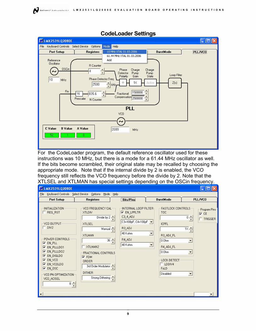
CodeLoader Settings
For the CodeLoader program, the default reference oscillator used for these instructions was 10 MHz, but there is a mode for a 61.44 MHz oscillator as well. If the bits become scrambled, their original state may be recalled by choosing the appropriate mode. Note that if the internal divide by 2 is enabled, the VCO frequency still reflects the VCO frequency before the divide by 2. Note that the XTLSEL and XTLMAN has special settings depending on the OSCin frequency.
9

L M X 2 5 3 1 L Q 2 0 8 0 E E V A L U A T I O N B O A R D O P E R A T I N G I N S T R U C T I O N S
CodeLoader is set up to load the registers and initialize the part in the correct way. R5 (INIT1) and R5 (INIT 2) are just the R5 register being used to properly initialize the part. So a single CNT+L should load the part.
The port setup tells CodeLoader what information goes where. If this is wrong, the part will not program. Although LPT1 is usually correct, CodeLoader does not autodetect the correct port. On some laptops, it may be LPT3.
10

L M X 2 5 3 1 L Q 2 0 8 0 E E V A L U A T I O N B O A R D O P E R A T I N G I N S T R U C T I O N S
Schematic
1 2 3 4 5 6
A
B
C
D
654321
D
C
B
A
Title
Number RevisionSize
B
Date: 6-Jan-2006 Sheet of File: C:\Documentum\Checkout\LMX2531LQEBPCB.ddb.ddbDrawn By:
R6
R16 R15 R13 R12 R11
R2_
LF
R8
C7
C2p
LF
C2_
LF C1_
LF
R14
LMX2531 Evaluation Board
LMX2531SLBCBPCB 01-06-2006
Dan Chappel l
C8
12
34
56
78
910
uWIRE
R10
C6
R2p
LF
C16
FRAME
Fout
Vcc
R21R19
R20
C1
R2
C12
C2
R3
C3
C17
R4
C9
C4
R5
C5
OSCin
C13
C18
C20
R7
R23
R22
Ftest/LD
C15
C22
R1
R9
TRIGGER
GND
1 23 45 67 8
POWER
C24
C14
C11
C19
C21
C23
Note that Any Component with Designator 100 or Higher is on the Bottom Side of the Board
C10
VccDIG1
NC2
GND3
NC4
NC5
VregBUF6
NC7
DATA8
CLK9
LE
10
CE
11
NC
12
NC
13
NC
14
NC
15
Vcc
VC
O16
Vre
gVC
O17
Vre
fVC
O18
GND 19GND 20Fout 21VccBUF 22Vtune 23CPout 24FLout 25VregPLL1 26VccPLL 27
GN
D34
NC
29Ft
est/L
D30
OSC
in31
OSC
in*
32T
est
33
NC
35V
regD
IG36
Vre
gPL
L228
SLG
137
SLG
238
SLG
339
U1
R18
R24
R17
C10
5
C10
0
C10
1
C10
3
C10
4C
102
VccVCO
VccDIG
VccPLL
VccBUF
VccVCO
VccPLL
VccBUF
Vcc
Vcc
VccDIG
11

L M X 2 5 3 1 L Q 2 0 8 0 E E V A L U A T I O N B O A R D O P E R A T I N G I N S T R U C T I O N S
Bill of Materials LMX2531EB Revision 1/3/2006
Item QTY Manufacturer Part # Size Tol Voltage Material Value Designators
19 Open Capacitors C2pLF, C2, C3, C4, C5, C9, C11, C14, C17,
C18, C19, C21, C24, C100, C101, C102, C103, C104, C105
6 Open Resistors R7, R8, R17, R19, R21, R24 0
1
n/a
Open Miscellaneous Ftest/LD 1 1 Kemet C0603C470J5GAC 603 5% 50V C0G 47pF C1_LF2 1 Kemet C0603C101J5GAC 603 5% 50V C0G 100pF C163 1 Kemet C0805C272J3GAC 805 5% 25V C0G 2.7nF C2_LF4 2 Kemet C0603C103J5RAC 603 5% 50V X7R 10nF C10, C235 4 Kemet C0603C104J3RAC 603 5% 25V X7R 100nF C6, C7, C12, C15 6 2 Kemet 603 10% 16V X7R 470nF C20, C227 1 Kemet C0603C105K4RAC 603 10% 16V X5R 1uF C88 1 Kemet 603 10% 6.3V X5R 4.7uF C139 1 Kemet C0805C106K8PAC 805 10% 10V X5R 10uF C1
10 1 Vishay CRCW0603000ZRT1 603 5% 0.1W Thick Film 0Ω R20 11 2 Panasonic P.22AHCT-ND 603 10% 0.1W Thick Film 0.22Ω R22, R23 12 2 Vishay CRCW06033R3JRT1 603 5% 0.1W Thick Film 3.3Ω R1, R18 13 4 Vishay CRCW0603100JRT1 603 5% 0.1W Thick Film 10Ω R2, R3, R4, R5 14 1 Vishay CRCW0603510JRT1 603 5% 0.1W Thick Film 51Ω R6 15 4 Vishay CRCW0603103JRT1 603 5% 0.1W Thick Film 10KΩ R9, R11, R13, R15 16 5 Vishay CRCW0603123JRT1 603 5% 0.1W Thick Film 12KΩ R2pLF, R10, R12, R14, R16 17 1 Vishay CRCW0603473JRT1 603 5% 0.1W Thick Film 47KΩ R2_LF 18 1 Comm Con Connectors HTSM3203-8G2 2X4 n/a n/a Metal/Plastic Header POWER19 1 FCI Electronics 52601-S10-8 2X5 n/a n/a Metal/Plastic Header uWire20 3 Johnson Components 142-0701-851 SMA n/a n/a Metal SMA Fout, OSCin, Vcc
21 1 National Semiconductor LMX2531LQEBPCB n/a n/a n/a FR4 62 mil Thick
PCB Board 1st Layer 10 mils n/a
22 1 National Semiconductor LMX2531 LLP36 n/a 2.7 Silicon LMX2531 U1
23 4 Com Con Connectors CCIJ255G 2-Pin n/a n/a Metal/Plastic Shunt Place Across: POWER: 1-2, 3-4, 5-6, 7-8
24 4 SPC Technology SPCS-8 0.156" n/a n/a Nylon Nylon Standoffs Place in 4 Holes in Corners of Board
C0603C474K4RAC
C0603C475K9PAC
12

L M X 2 5 3 1 L Q 2 0 8 0 E E V A L U A T I O N B O A R D O P E R A T I N G I N S T R U C T I O N S
Top Layer
13

L M X 2 5 3 1 L Q 2 0 8 0 E E V A L U A T I O N B O A R D O P E R A T I N G I N S T R U C T I O N S
Mid Layer 1 "Ground Plane" (15 Mils Down FR4)
14

L M X 2 5 3 1 L Q 2 0 8 0 E E V A L U A T I O N B O A R D O P E R A T I N G I N S T R U C T I O N S
Mid Layer 2 "Power"
15

L M X 2 5 3 1 L Q 2 0 8 0 E E V A L U A T I O N B O A R D O P E R A T I N G I N S T R U C T I O N S
Bottom Layer "Signal"
Note: Total Board Thickness = 61 mils
16

L M X 2 5 3 1 L Q 2 0 8 0 E E V A L U A T I O N B O A R D O P E R A T I N G I N S T R U C T I O N S
17
Top Build Diagram
IMPORTANT NOTICE
Texas Instruments Incorporated and its subsidiaries (TI) reserve the right to make corrections, modifications, enhancements, improvements,and other changes to its products and services at any time and to discontinue any product or service without notice. Customers shouldobtain the latest relevant information before placing orders and should verify that such information is current and complete. All products aresold subject to TI’s terms and conditions of sale supplied at the time of order acknowledgment.
TI warrants performance of its hardware products to the specifications applicable at the time of sale in accordance with TI’s standardwarranty. Testing and other quality control techniques are used to the extent TI deems necessary to support this warranty. Except wheremandated by government requirements, testing of all parameters of each product is not necessarily performed.
TI assumes no liability for applications assistance or customer product design. Customers are responsible for their products andapplications using TI components. To minimize the risks associated with customer products and applications, customers should provideadequate design and operating safeguards.
TI does not warrant or represent that any license, either express or implied, is granted under any TI patent right, copyright, mask work right,or other TI intellectual property right relating to any combination, machine, or process in which TI products or services are used. Informationpublished by TI regarding third-party products or services does not constitute a license from TI to use such products or services or awarranty or endorsement thereof. Use of such information may require a license from a third party under the patents or other intellectualproperty of the third party, or a license from TI under the patents or other intellectual property of TI.
Reproduction of TI information in TI data books or data sheets is permissible only if reproduction is without alteration and is accompaniedby all associated warranties, conditions, limitations, and notices. Reproduction of this information with alteration is an unfair and deceptivebusiness practice. TI is not responsible or liable for such altered documentation. Information of third parties may be subject to additionalrestrictions.
Resale of TI products or services with statements different from or beyond the parameters stated by TI for that product or service voids allexpress and any implied warranties for the associated TI product or service and is an unfair and deceptive business practice. TI is notresponsible or liable for any such statements.
TI products are not authorized for use in safety-critical applications (such as life support) where a failure of the TI product would reasonablybe expected to cause severe personal injury or death, unless officers of the parties have executed an agreement specifically governingsuch use. Buyers represent that they have all necessary expertise in the safety and regulatory ramifications of their applications, andacknowledge and agree that they are solely responsible for all legal, regulatory and safety-related requirements concerning their productsand any use of TI products in such safety-critical applications, notwithstanding any applications-related information or support that may beprovided by TI. Further, Buyers must fully indemnify TI and its representatives against any damages arising out of the use of TI products insuch safety-critical applications.
TI products are neither designed nor intended for use in military/aerospace applications or environments unless the TI products arespecifically designated by TI as military-grade or "enhanced plastic." Only products designated by TI as military-grade meet militaryspecifications. Buyers acknowledge and agree that any such use of TI products which TI has not designated as military-grade is solely atthe Buyer's risk, and that they are solely responsible for compliance with all legal and regulatory requirements in connection with such use.
TI products are neither designed nor intended for use in automotive applications or environments unless the specific TI products aredesignated by TI as compliant with ISO/TS 16949 requirements. Buyers acknowledge and agree that, if they use any non-designatedproducts in automotive applications, TI will not be responsible for any failure to meet such requirements.
Following are URLs where you can obtain information on other Texas Instruments products and application solutions:
Products Applications
Audio www.ti.com/audio Automotive and Transportation www.ti.com/automotive
Amplifiers amplifier.ti.com Communications and Telecom www.ti.com/communications
Data Converters dataconverter.ti.com Computers and Peripherals www.ti.com/computers
DLP® Products www.dlp.com Consumer Electronics www.ti.com/consumer-apps
DSP dsp.ti.com Energy and Lighting www.ti.com/energy
Clocks and Timers www.ti.com/clocks Industrial www.ti.com/industrial
Interface interface.ti.com Medical www.ti.com/medical
Logic logic.ti.com Security www.ti.com/security
Power Mgmt power.ti.com Space, Avionics and Defense www.ti.com/space-avionics-defense
Microcontrollers microcontroller.ti.com Video and Imaging www.ti.com/video
RFID www.ti-rfid.com
OMAP Mobile Processors www.ti.com/omap
Wireless Connectivity www.ti.com/wirelessconnectivity
TI E2E Community Home Page e2e.ti.com
Mailing Address: Texas Instruments, Post Office Box 655303, Dallas, Texas 75265Copyright © 2012, Texas Instruments Incorporated