lna implementation federico perini aa-low technical progress meeting medicina, 22-23 september 2012
TRANSCRIPT

LNA implementation
Federico PeriniAA-low Technical Progress MeetingMedicina, 22-23 September 2012

50Ohm AAlo LNA
Schematic, bill of materials and layout.
Fig 1. LNA schematic.
Table 1. Bill of materials.
Fig 2. Top view layout (Q2 is mounted on the bottom layer).
RFin RFout DCin
Q1
Q2
C1 C2
C3 C4
C5 C6
L1
L2
C1 Murata, 150pF, 0603, GRM1885C1H151JA01C2 Murata, 150pF, 0603, GRM1885C1H151JA01C3 Murata, 150pF, 0603, GRM1885C1H151JA01C4 Murata, 100nF, 0603, GRM188R71H104KA93C5 AVX, 4.7uF, Case B, TAJB475K010RNJC6 AVX, 1uF, Case B, TAJB105K035RNJL1 Coilcraft, 1.2uF, 1008LS-122XJLBL2 Minicircuits, RF choke, ADCH-80AQ1 RFMD, MMIC Amplifier, SPF-5122ZQ2 National Semiconductors, LDO regulator, LP2950
3V, 60mA (included LDO)

LNA for Vivaldi (August 2011)
2 samples shipped to Perth for (active) antenna pattern
measurement on mast
1 LNA for measurement and test (presented in Perth September 2011)

General description The LNA is based on the RF Micro Devices SPF-5122Z low noise MMIC amplifier. The biasing network (input and output DC block and the output choke) has been designed in order to optimise the LNA performance in the desired frequency band 50-450MHz. DC power is provided through the output RF connector. Both +3V and +5V DC supplies are allowed by the MMIC but, in order to reduce both power consumption and noise figure, the former (3V, 58mA) has been chosen. To keep the correct MMIC bias point, which has to be independent from the DC losses of the output coaxial cable, a low dropout (LDO) voltage regulator (LP2950) has been included in the LNA. If the RFI scenario would request more dynamic range, the +5V bias point has to be chosen. In order to do that, the only operation requested is to replace the LDO regulator. The LNA doesn’t include any gain equalization network since it will be included further in the receiver chain.
The LNA is based on the following technological choices: 1. Printed circuit board (PCB) on FR4 (h=1.6mm, t=17.5um, r=4.7). 2. PCB production through LPKF milling machine. 3. Via holes metallisation with ProConduct paste. 4. SMA 50Ohm input and output connectors, LNA version for measurements in the lab. 5. TNC 50Ohm input and output connectors, LNA version to be mounted inside the Vivaldi antenna.
Main specifications
Table 1. Summary of the main LNA specifications.
Item Symbol Conditions Nom Min Max Unit Gain G 50-450MHz
21.9 25.5 dB
Gain Variation ∆G 50-450MHz ±1.8 dB
Input Match IRL 50-450MHz 6.5 dB
Output Match ORL 50-450MHz 19.5 dB
Reverse Isolation ISO 50-450MHz 27 dB
Noise Figure NF 50-450MHz 0.5 dB
Noise Temperature Te 50-450MHz 35 K
Compression point OP1dB 50-450MHz
(200-450MHz) +12 (+18) dBm
3rd Order Intercept Point OIP3 50-450MHz +30.5 dBm
2nd Order Intercept Point OIP2 50-225MHz Input
(100-450MHz Output) +42 dBm
Current Consumption Idd Include LDO quiescent current 60 mA
Power Supply Vdd Internal 3V LDO regulator 3.5 30 V
LNA Datasheet (March 2012)
Schematic, bill of materials and layout.
Fig 1. LNA schematic.
Table 1. Bill of materials. C1 Murata, 150pF, 0603, GRM1885C1H151JA01 C2 Murata, 150pF, 0603, GRM1885C1H151JA01 C3 Murata, 150pF, 0603, GRM1885C1H151JA01 C4 Murata, 100nF, 0603, GRM188R71H104KA93 C5 AVX, 4.7uF, Case B, TAJB475K010RNJ C6 AVX, 1uF, Case B, TAJB105K035RNJ L1 Coilcraft, 1.2uF, 1008LS-122XJLB L2 Minicircuits, RF choke, ADCH-80A Q1 RFMD, MMIC Amplifier, SPF-5122Z Q2 National Semiconductors, LDO regulator, LP2950
Fig 2. Top view layout (Q2 is mounted on the bottom layer).
RFin RFout DCin
Q1
Q2
C1 C2
C3 C4
C5 C6
L1
L2

LNA with RFI (Medicina, May 2012)
RFI measurements performed with both SA and Power Meter
45° E/W 135° N/SP (dBm) -0.8 -4.4 -10.6 -2.2
15dB below the P1dB (@FM, 3V)

LNA for AAVS0 (June 2012)
32 LNA assembled and tested for (active) embedded pattern
measurement and/or mutual coupling
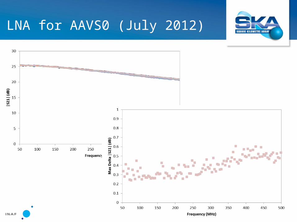
LNA for AAVS0 (July 2012)

LNA for AAVS0 (July 2012)

LNA for AAVS0 (July 2012)

AAVS0 LNA housing

Conclusion
• LNA for both single antenna and AAVS0 array measurements produced and delivered on time
• For AAVS1 (500 pieces):o Integration of 2 (and 3?) stageo Integration of O-TX?o LNA replication on PCB (FR4)o Avoid the connectors?o Different housing?
• For AAVS2 (min 7K pieces)o Custom MMIC?o Avoid the connectors!o Different housing!o Integration of O-TX?

Thanks!

LNA: S-parameters (1)
Meas. notes: Equipment: HP8753C with HP85047 test setFull 2 port Calibration, LNA Bias from port 2 of the VNA

LNA: S-parameters (2)
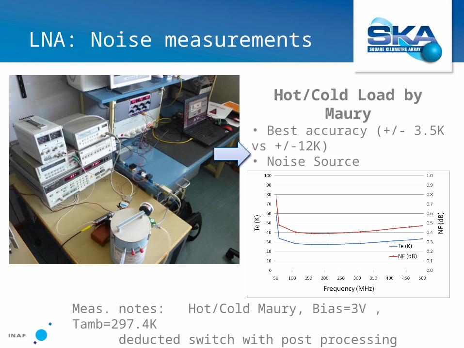
LNA: Noise measurements
Meas. notes: Hot/Cold Maury, Bias=3V , Tamb=297.4Kdeducted switch with post processing( reference plane = IN Connector)
Hot/Cold Load by Maury• Best accuracy (+/- 3.5K vs +/-12K)• Noise Source (re)calibration (ENR)• More ENR points (i.e. standard ENR table: 0.01, 0.1, 1, … GHz)

LNA: Dynamic measurements
All measurements at: 3V, 58mA 174mW
2-3 dB IP3 improvement at 5V, 90mA 450mW!!