local oscillator: phase-locked source and multiplier systemdemerson/almapbk/.../chap7.2.pdf ·...
TRANSCRIPT
Page 1 of 23
ALMA Project Book, Chapter 7, Section 2
Local Oscillator: Phase-Locked Source and Multiplier System
Richard Bradley, Dorsey Thacker, Eric Bryerton, and Kamaljeet Saini
August 1, 2000
Revision History:
Summary
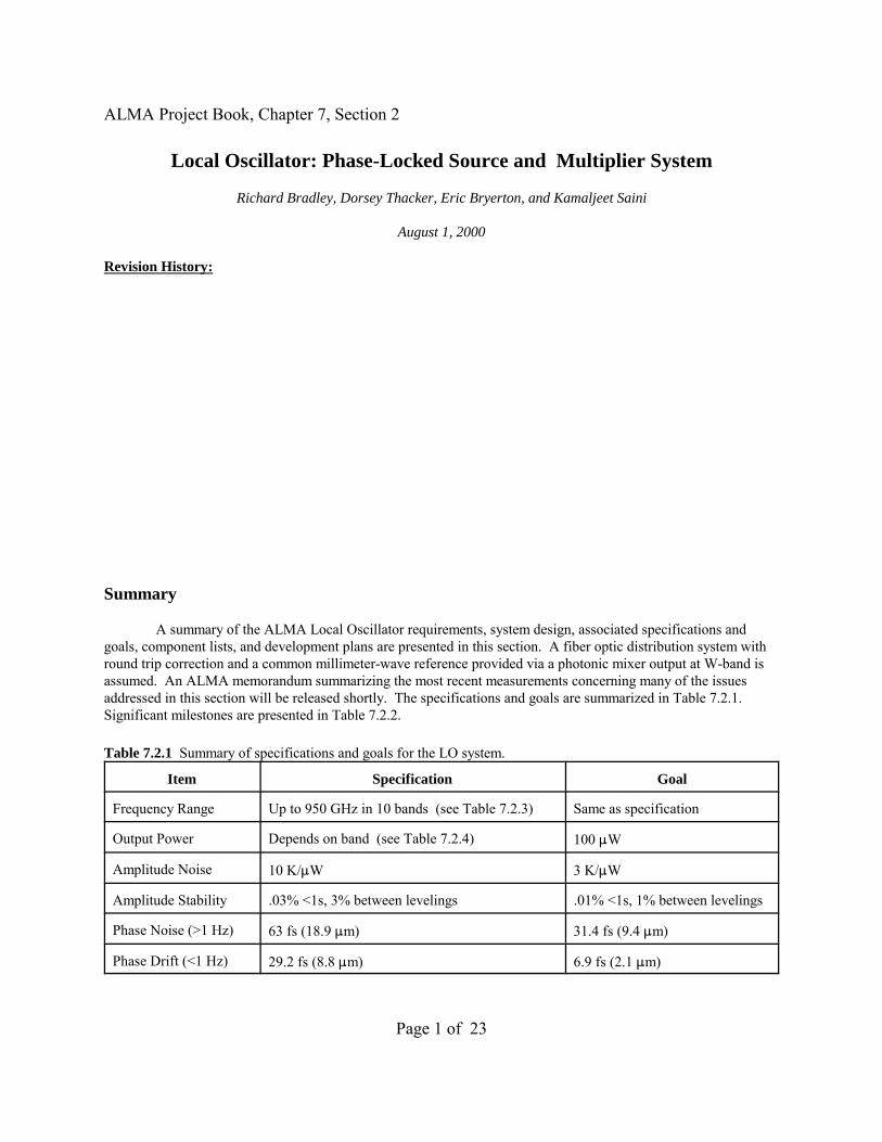
A summary of the ALMA Local Oscillator requirements, system design, associated specifications andgoals, component lists, and development plans are presented in this section. A fiber optic distribution system withround trip correction and a common millimeter-wave reference provided via a photonic mixer output at W-band isassumed. An ALMA memorandum summarizing the most recent measurements concerning many of the issuesaddressed in this section will be released shortly. The specifications and goals are summarized in Table 7.2.1. Significant milestones are presented in Table 7.2.2.
Table 7.2.1 Summary of specifications and goals for the LO system.
Item Specification Goal
Frequency Range Up to 950 GHz in 10 bands (see Table 7.2.3) Same as specification
Output Power Depends on band (see Table 7.2.4) 100 �W
Amplitude Noise 10 K/�W 3 K/�W
Amplitude Stability .03% <1s, 3% between levelings .01% <1s, 1% between levelings
Phase Noise (>1 Hz) 63 fs (18.9 �m) 31.4 fs (9.4 �m)
Phase Drift (<1 Hz) 29.2 fs (8.8 �m) 6.9 fs (2.1 �m)
Page 2 of 23
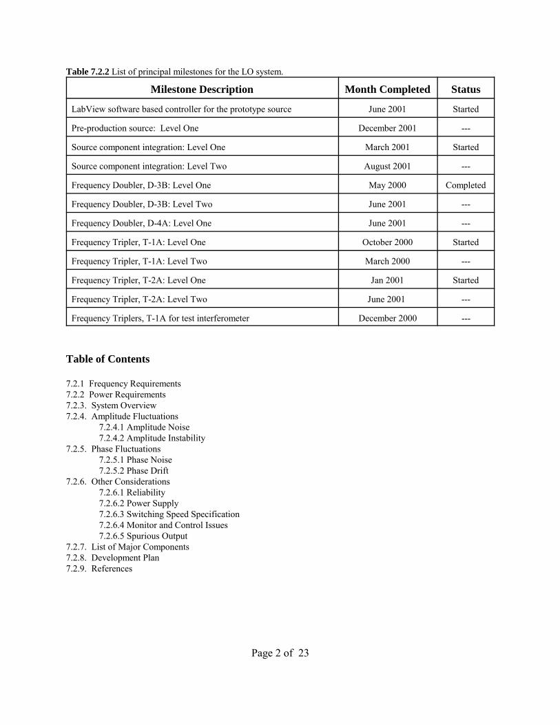
Table 7.2.2 List of principal milestones for the LO system.
Milestone Description Month Completed Status
LabView software based controller for the prototype source June 2001 Started
Pre-production source: Level One December 2001 ---
Source component integration: Level One March 2001 Started
Source component integration: Level Two August 2001 ---
Frequency Doubler, D-3B: Level One May 2000 Completed
Frequency Doubler, D-3B: Level Two June 2001 ---
Frequency Doubler, D-4A: Level One June 2001 ---
Frequency Tripler, T-1A: Level One October 2000 Started
Frequency Tripler, T-1A: Level Two March 2000 ---
Frequency Tripler, T-2A: Level One Jan 2001 Started
Frequency Tripler, T-2A: Level Two June 2001 ---
Frequency Triplers, T-1A for test interferometer December 2000 ---
Table of Contents
7.2.1 Frequency Requirements7.2.2 Power Requirements7.2.3. System Overview7.2.4. Amplitude Fluctuations
7.2.4.1 Amplitude Noise7.2.4.2 Amplitude Instability
7.2.5. Phase Fluctuations7.2.5.1 Phase Noise7.2.5.2 Phase Drift
7.2.6. Other Considerations7.2.6.1 Reliability7.2.6.2 Power Supply7.2.6.3 Switching Speed Specification7.2.6.4 Monitor and Control Issues7.2.6.5 Spurious Output
7.2.7. List of Major Components7.2.8. Development Plan7.2.9. References
Page 3 of 23
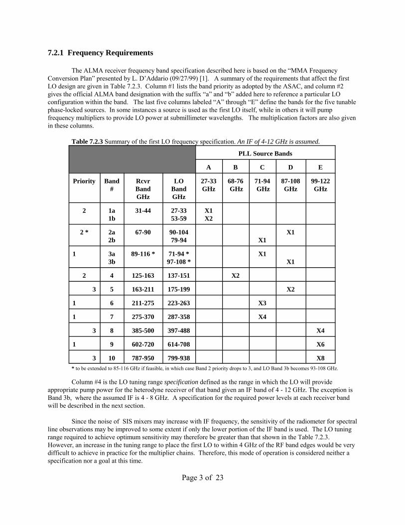
7.2.1 Frequency Requirements
The ALMA receiver frequency band specification described here is based on the �MMA FrequencyConversion Plan� presented by L. D�Addario (09/27/99) [1]. A summary of the requirements that affect the firstLO design are given in Table 7.2.3. Column #1 lists the band priority as adopted by the ASAC, and column #2gives the official ALMA band designation with the suffix �a� and �b� added here to reference a particular LOconfiguration within the band. The last five columns labeled �A� through �E� define the bands for the five tunablephase-locked sources. In some instances a source is used as the first LO itself, while in others it will pumpfrequency multipliers to provide LO power at submillimeter wavelengths. The multiplication factors are also givenin these columns.
Table 7.2.3 Summary of the first LO frequency specification. An IF of 4-12 GHz is assumed.
PLL Source Bands
A B C D E
Priority Band#
RcvrBandGHz
LOBandGHz
27-33GHz
68-76 GHz
71-94 GHz
87-108GHz
99-122GHz
2 1a1b
31-44 27-3353-59
X1X2
2 * 2a2b
67-90 90-10479-94 X1
X1
1 3a3b
89-116 * 71-94 *97-108 *
X1X1
2 4 125-163 137-151 X2
3 5 163-211 175-199 X2
1 6 211-275 223-263 X3
1 7 275-370 287-358 X4
3 8 385-500 397-488 X4
1 9 602-720 614-708 X6
3 10 787-950 799-938 X8* to be extended to 85-116 GHz if feasible, in which case Band 2 priority drops to 3, and LO Band 3b becomes 93-108 GHz.
Column #4 is the LO tuning range specification defined as the range in which the LO will provideappropriate pump power for the heterodyne receiver of that band given an IF band of 4 - 12 GHz. The exception isBand 3b, where the assumed IF is 4 - 8 GHz. A specification for the required power levels at each receiver bandwill be described in the next section.
Since the noise of SIS mixers may increase with IF frequency, the sensitivity of the radiometer for spectralline observations may be improved to some extent if only the lower portion of the IF band is used. The LO tuningrange required to achieve optimum sensitivity may therefore be greater than that shown in the Table 7.2.3. However, an increase in the tuning range to place the first LO to within 4 GHz of the RF band edges would be verydifficult to achieve in practice for the multiplier chains. Therefore, this mode of operation is considered neither aspecification nor a goal at this time.
Page 4 of 23
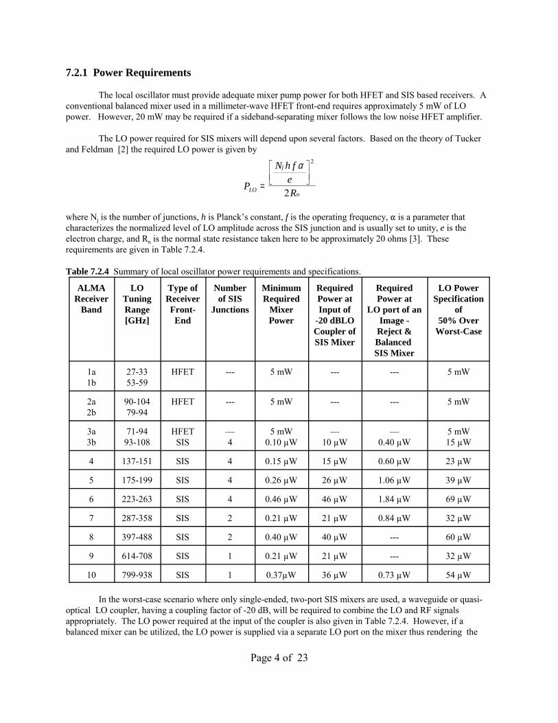
7.2.1 Power Requirements
The local oscillator must provide adequate mixer pump power for both HFET and SIS based receivers. Aconventional balanced mixer used in a millimeter-wave HFET front-end requires approximately 5 mW of LO power. However, 20 mW may be required if a sideband-separating mixer follows the low noise HFET amplifier.
The LO power required for SIS mixers will depend upon several factors. Based on the theory of Tuckerand Feldman [2] the required LO power is given by
P
N h feRLO
j
n=
�
���
��α 2
2
where Nj is the number of junctions, h is Planck�s constant, f is the operating frequency, � is a parameter thatcharacterizes the normalized level of LO amplitude across the SIS junction and is usually set to unity, e is theelectron charge, and Rn is the normal state resistance taken here to be approximately 20 ohms [3]. Theserequirements are given in Table 7.2.4.
Table 7.2.4 Summary of local oscillator power requirements and specifications.
ALMAReceiver
Band
LOTuningRange[GHz]
Type ofReceiverFront-End
Numberof SIS
Junctions
MinimumRequired
MixerPower
RequiredPower atInput of
-20 dBLOCoupler ofSIS Mixer
RequiredPower at
LO port of anImage -
Reject &Balanced SIS Mixer
LO PowerSpecification
of50% Over
Worst-Case
1a1b
27-3353-59
HFET --- 5 mW --- --- 5 mW
2a2b
90-10479-94
HFET --- 5 mW --- --- 5 mW
3a3b
71-9493-108
HFETSIS
�4
5 mW0.10 µW
�10 µW
�0.40 µW
5 mW15 µW
4 137-151 SIS 4 0.15 µW 15 µW 0.60 µW 23 µW
5 175-199 SIS 4 0.26 µW 26 µW 1.06 µW 39 µW
6 223-263 SIS 4 0.46 µW 46 µW 1.84 µW 69 µW
7 287-358 SIS 2 0.21 µW 21 µW 0.84 µW 32 µW
8 397-488 SIS 2 0.40 µW 40 µW --- 60 µW
9 614-708 SIS 1 0.21 µW 21 µW --- 32 µW
10 799-938 SIS 1 0.37µW 36 µW 0.73 µW 54 µW
In the worst-case scenario where only single-ended, two-port SIS mixers are used, a waveguide or quasi-optical LO coupler, having a coupling factor of -20 dB, will be required to combine the LO and RF signalsappropriately. The LO power required at the input of the coupler is also given in Table 7.2.4. However, if abalanced mixer can be utilized, the LO power is supplied via a separate LO port on the mixer thus rendering the
Page 5 of 23
coupler unnecessary. Column #7 in Table 7.2.4 lists the power requirements for a balanced mixer configuration thatis both image separating and balanced. The last column is a suggested specification per RF band based upon a 50percent overhead for the worst-case conditions. The LO power goal will be 100 µW per band to ensure adequatepower to overcome losses within the mixer block.
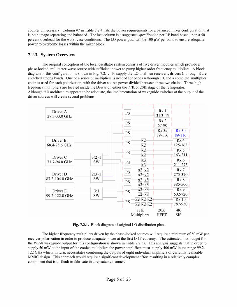
7.2.3. System Overview
The original conception of the local oscillator system consists of five driver modules which provide aphase-locked, millimeter-wave source with sufficient power to pump higher order frequency multipliers. A blockdiagram of this configuration is shown in Fig. 7.2.1. To supply the LO to all ten receivers, drivers C through E areswitched among bands. One or a series of multipliers is needed for bands 4 through 10, and a complete multiplierchain is used for each polarization, with the driver source power divided between these two chains. These highfrequency multipliers are located inside the Dewar on either the 77K or 20K stage of the refrigerator. Although this architecture appears to be adequate, the implementation of waveguide switches at the output of thedriver sources will create several problems.
77KMultipliers
20KHFET
4KSIS
Driver B68.4-75.6 GHz
Driver D87.2-104.0 GHz
Rx 10787-950x2 x2 x2
x2x2 x2x2 x3x2 x3 Rx 9
602-720
x2 x3x2 x3
Rx 8385-500
x2 x2x2 x2 Rx 7
275-370
x3x3 Rx 6
211-275
x2x2 Rx 5
163-211
x2x2
Rx 4125-163
3(2):1SW
Rx 267-90
Rx 131.3-45
PS
PS
PS
PS
PS
PS
PS
PS
PS
PS
3:1SW
2(3):1SW
Driver C71.7-94.0 GHz
Driver E99.2-122.0 GHz
Driver A27.3-33.0 GHz
Rx 3b89-116
Rx 3a89-116
Fig. 7.2.1. Block diagram of original LO distribution plan.
The higher frequency multipliers driven by the phase-locked sources will require a minimum of 50 mW perreceiver polarization in order to produce adequate power at the first LO frequency. The estimated loss budget forthe WR-8 waveguide output for this configuration is shown in Table 7.2.5a. This analysis suggests that in order tosupply 50 mW at the input of the cooled multipliers the power amplifiers must supply 400 mW in the range 99.2-122 GHz which, in turn, necessitates combining the outputs of eight individual amplifiers of currently realizableMMIC design. This approach would require a significant development effort resulting in a relatively complexcomponent that is difficult to fabricate in a repeatable manner.
Page 6 of 23
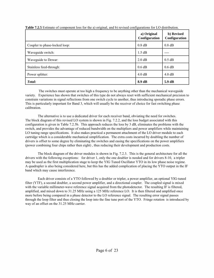
Table 7.2.5 Estimate of component loss for the a) original, and b) revised configurations for LO distribution.
a) OriginalConfiguration
b) RevisedConfiguration
Coupler to phase-locked loop: 0.8 dB 0.8 dB
Waveguide switch: 1.5 dB ----
Waveguide to Dewar: 2.0 dB 0.5 dB
Stainless feed-through: 0.6 dB 0.6 dB
Power splitter: 4.0 dB 4.0 dB
Total: 8.9 dB 5.9 dB
The switches must operate at too high a frequency to be anything other than the mechanical waveguidevariety. Experience has shown that switches of this type do not always reset with sufficient mechanical precision toconstrain variations in signal reflections from one switch cycle to another, thus introducing sporadic phase errors. This is particularly important for Band 3, which will usually be the receiver of choice for fast switching phasecalibration.
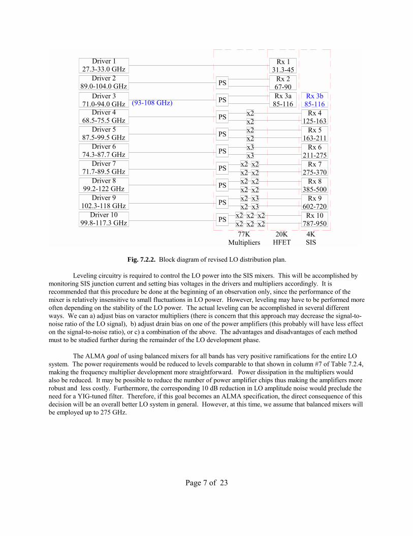
The alternative is to use a dedicated driver for each receiver band, obviating the need for switches.The block diagram of this revised LO system is shown in Fig. 7.2.2, and the loss budget associated with thisconfiguration is given in Table 7.2.5b. This approach reduces the loss by 3 dB, eliminates the problems with theswitch, and provides the advantage of reduced bandwidth on the multipliers and power amplifiers while maintainingLO tuning range specifications. It also makes practical a permanent attachment of the LO driver module to eachcartridge which is a considerable mechanical simplification. The extra costs incurred by doubling the number ofdrivers is offset to some degree by eliminating the switches and easing the specifications on the power amplifiers(power combining four chips rather then eight) , thus reducing their development and production costs.
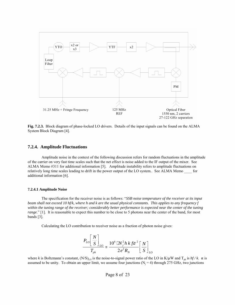
The block diagram of the driver modules is shown in Fig. 7.2.3. This is the general architecture for all thedrivers with the following exceptions: for driver 1, only the one doubler is needed and for drivers 8-10, a triplermay be used as the first multiplication stage to keep the YIG Tuned Oscillator YTO in its low phase noise regime. A quadrupler is also being considered here, but this has the added complication of placing the YTO output in the IFband which may cause interference.
Each driver consists of a YTO followed by a doubler or tripler, a power amplifier, an optional YIG-tunedfilter (YTF), a second doubler, a second power amplifier, and a directional coupler. The coupled signal is mixedwith the variable millimeter-wave reference signal acquired from the photodetector. The resulting IF is filtered,amplified, and mixed down to 31.25 MHz using a 125 MHz reference LO. It is then filtered and amplified oncemore before being compared in a phase detector to the LO reference signal. The resulting error signal passesthrough the loop filter and thus closing the loop into the fine tune port of the YTO. Fringe rotation is introduced byway of an offset on the 31.25 MHz carrier.
Page 7 of 23
77KMultipliers
20KHFET
4KSIS
Rx 10787-950x2 x2 x2
x2x2 x2x2 x3x2 x3 Rx 9
602-720
Rx 8385-500
x2 x2x2 x2 Rx 7
275-370
x3x3 Rx 6
211-275
x2x2 Rx 5
163-211
x2x2
Rx 4125-163
Rx 267-90
Rx 131.3-45
PS
PS
PS
PS
PS
PS
PS
PS
PS
Driver 127.3-33.0 GHz
Driver 289.0-104.0 GHz
Driver 468.5-75.5 GHz
Driver 587.5-99.5 GHz
Driver 674.3-87.7 GHz
Driver 771.7-89.5 GHz
Driver 899.2-122 GHz
Driver 9102.3-118 GHz
Driver 1099.8-117.3 GHz
x2 x2x2 x2
(93-108 GHz)Rx 3b85-116
Rx 3a85-116
Driver 371.0-94.0 GHz
Fig. 7.2.2. Block diagram of revised LO distribution plan.
Leveling circuitry is required to control the LO power into the SIS mixers. This will be accomplished bymonitoring SIS junction current and setting bias voltages in the drivers and multipliers accordingly. It isrecommended that this procedure be done at the beginning of an observation only, since the performance of themixer is relatively insensitive to small fluctuations in LO power. However, leveling may have to be performed moreoften depending on the stability of the LO power. The actual leveling can be accomplished in several differentways. We can a) adjust bias on varactor multipliers (there is concern that this approach may decrease the signal-to-noise ratio of the LO signal), b) adjust drain bias on one of the power amplifiers (this probably will have less effecton the signal-to-noise ratio), or c) a combination of the above. The advantages and disadvantages of each methodmust to be studied further during the remainder of the LO development phase.
The ALMA goal of using balanced mixers for all bands has very positive ramifications for the entire LOsystem. The power requirements would be reduced to levels comparable to that shown in column #7 of Table 7.2.4,making the frequency multiplier development more straightforward. Power dissipation in the multipliers wouldalso be reduced. It may be possible to reduce the number of power amplifier chips thus making the amplifiers morerobust and less costly. Furthermore, the corresponding 10 dB reduction in LO amplitude noise would preclude theneed for a YIG-tuned filter. Therefore, if this goal becomes an ALMA specification, the direct consequence of thisdecision will be an overall better LO system in general. However, at this time, we assume that balanced mixers willbe employed up to 275 GHz.
Page 8 of 23
YTO YTF x2
Optical Fiber1550 nm, 2 carriers
27-122 GHz separation
125 MHzREF
LoopFilter
x2 orx3
PM
31.25 MHz + Fringe Frequency
Fig. 7.2.3. Block diagram of phase-locked LO drivers. Details of the input signals can be found on the ALMASystem Block Diagram [4].
7.2.4. Amplitude Fluctuations
Amplitude noise in the context of the following discussion refers for random fluctuations in the amplitudeof the carrier on very fast time scales such that the net effect is noise added to the IF output of the mixer. SeeALMA Memo #311 for additional information [5]. Amplitude instability refers to amplitude fluctuations onrelatively long time scales leading to drift in the power output of the LO system.. See ALMA Memo ____ foradditional information [6].
7.2.4.1 Amplitude Noise
The specification for the receiver noise is as follows: �SSB noise temperature of the receiver at its inputbeam shall not exceed 10 hf/k, where h and k are the usual physical constants. This applies to any frequency fwithin the tuning range of the receiver; considerably better performance is expected near the center of the tuningrange.� [1]. It is reasonable to expect this number to be close to 5 photons near the center of the band, for mostbands [3].
Calculating the LO contribution to receiver noise as a fraction of photon noise gives:
PNS
TN h k fe R
NS
LOLO
ph
j
N LO
�
���
�� =⋅ �
���
��10
2
6 2 2
2
α
where k is Boltzmann�s constant, (N/S)LO is the noise-to-signal power ratio of the LO in K/�W and Tph is hf / k. � isassumed to be unity. To obtain an upper limit, we assume four junctions (Nj = 4) through 275 GHz, two junctions
Page 9 of 23
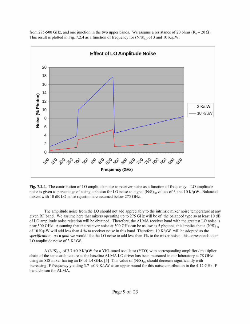
from 275-500 GHz, and one junction in the two upper bands. We assume a resistance of 20 ohms (Rn = 20 �). This result is plotted in Fig. 7.2.4 as a function of frequency for (N/S)LO of 3 and 10 K/�W.
Effect of LO Amplitude Noise
0
2
4
6
8
10
12
14
16
18
20
100
150
200
250
300
350
400
450
500
550
600
650
700
750
800
850
900
950
Frequency (GHz)
Noi
se (%
Pho
ton)
3 K/uW10 K/uW
Fig. 7.2.4. The contribution of LO amplitude noise to receiver noise as a function of frequency. LO amplitudenoise is given as percentage of a single photon for LO noise-to-signal (N/S)LO values of 3 and 10 K/�W. Balancedmixers with 10 dB LO noise rejection are assumed below 275 GHz.
The amplitude noise from the LO should not add appreciably to the intrinsic mixer noise temperature at anygiven RF band. We assume here that mixers operating up to 275 GHz will be of the balanced type so at least 10 dBof LO amplitude noise rejection will be obtained. Therefore, the ALMA receiver band with the greatest LO noise isnear 500 GHz. Assuming that the receiver noise at 500 GHz can be as low as 5 photons, this implies that a (N/S)LO
of 10 K/�W will add less than 4 % to receiver noise in this band. Therefore, 10 K/�W will be adopted as thespecification. As a goal we would like the LO noise to add less than 1% to the mixer noise; this corresponds to anLO amplitude noise of 3 K/�W.
A (N/S)LO of 3.7 ±0.9 K/�W for a YIG-tuned oscillator (YTO) with corresponding amplifier / multiplierchain of the same architecture as the baseline ALMA LO driver has been measured in our laboratory at 78 GHzusing an SIS mixer having an IF of 1.4 GHz. [5] This value of (N/S)LO should decrease significantly withincreasing IF frequency yielding 3.7 ±0.9 K/�W as an upper bound for this noise contribution in the 4-12 GHz IFband chosen for ALMA.
Page 10 of 23
Measured Receiver Temperature vs SIS Mixer DC Current (230 GHz)
58
60
62
64
66
68
70
72
74
52 58.5 65 71.5 78 84.5
Idc (uA)
Tr D
SB (K
)
Additional filtering of the LO signal is also being considered. The LO amplitude noise contribution willalso be reduced by the intrinsic filtering action of the multipliers. The instantaneous bandwidth of a varactor-typefrequency multiplier is limited to only about one percent or less of the operating frequency due to the nature of theimpedance matching which requires an adjustment of the varactor bias to tune the multiplier over the required LOband. We must verify that the ALMA specification can be met over the entire LO tuning range with only theintrinsic multiplier filtering. However, it might be necessary to use an electronically-tuned YIG-filter (YTF) in the40-60 GHz range. We do not advocate meeting the goal by using mechanically tuned cavity filters at the YTOdriver output (65-120 GHz).
7.2.4.2. Amplitude Instability
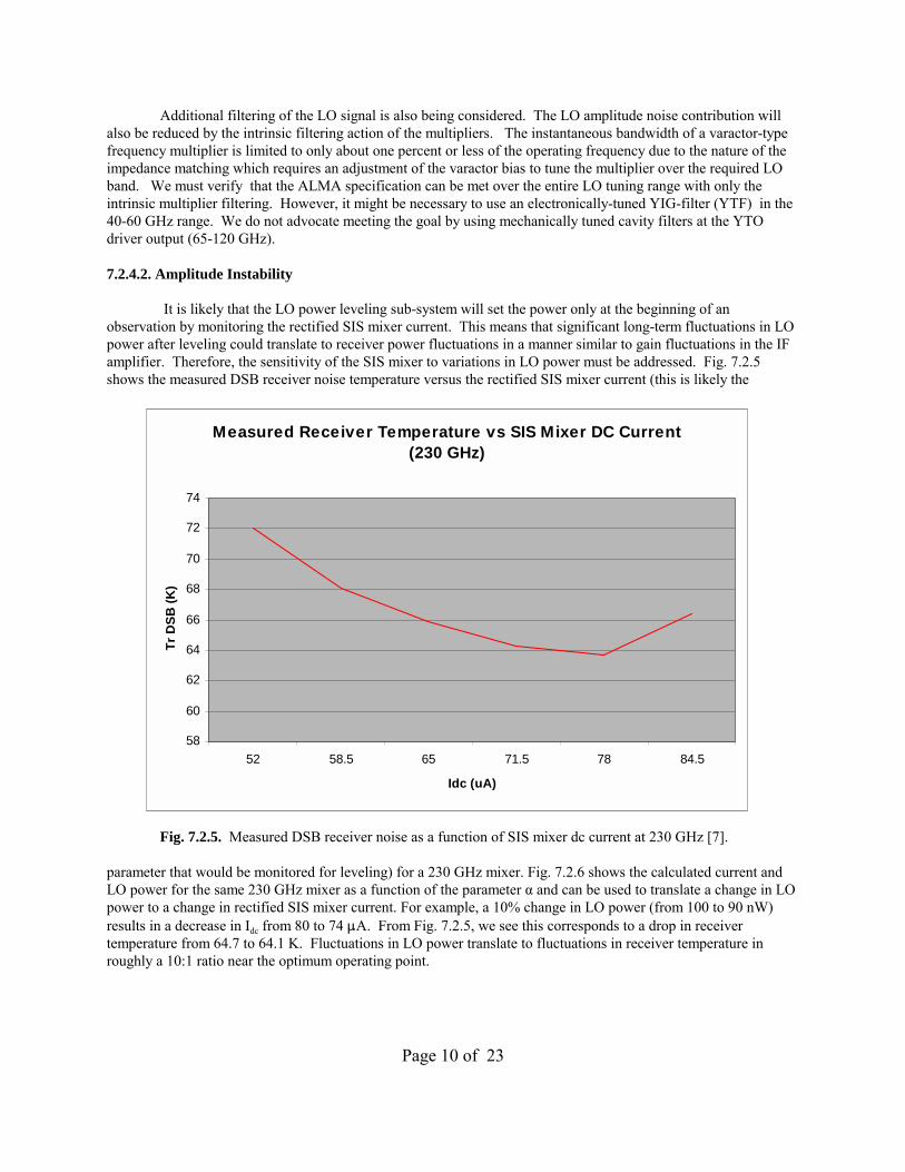
It is likely that the LO power leveling sub-system will set the power only at the beginning of anobservation by monitoring the rectified SIS mixer current. This means that significant long-term fluctuations in LOpower after leveling could translate to receiver power fluctuations in a manner similar to gain fluctuations in the IFamplifier. Therefore, the sensitivity of the SIS mixer to variations in LO power must be addressed. Fig. 7.2.5shows the measured DSB receiver noise temperature versus the rectified SIS mixer current (this is likely the
Fig. 7.2.5. Measured DSB receiver noise as a function of SIS mixer dc current at 230 GHz [7].
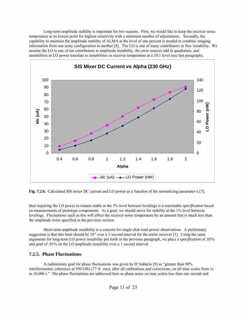
parameter that would be monitored for leveling) for a 230 GHz mixer. Fig. 7.2.6 shows the calculated current andLO power for the same 230 GHz mixer as a function of the parameter α and can be used to translate a change in LOpower to a change in rectified SIS mixer current. For example, a 10% change in LO power (from 100 to 90 nW)results in a decrease in Idc from 80 to 74 �A. From Fig. 7.2.5, we see this corresponds to a drop in receivertemperature from 64.7 to 64.1 K. Fluctuations in LO power translate to fluctuations in receiver temperature inroughly a 10:1 ratio near the optimum operating point.
Page 11 of 23
Long-term amplitude stability is important for two reasons. First, we would like to keep the receiver noisetemperature at its lowest point for highest sensitivity with a minimum number of adjustments. Secondly, thecapability to maintain the amplitude stability of ALMA at the level of one percent is needed to combine imaginginformation from one array configuration to another [8]. The LO is one of many contributors to flux instability. Weassume the LO is one of ten contributors to amplitude instability, the error sources add in quadrature, andinstabilities in LO power translate to instabilities in receiver temperature at a 10:1 level (see last paragraph),
SIS Mixer DC Current vs Alpha (230 GHz)
0
10
20
30
40
50
60
70
80
90
100
0.4 0.6 0.8 1 1.2 1.4 1.6 1.8 2
Alpha
Idc
(uA
)
0
20
40
60
80
100
120
140
LO P
ower
(nW
)
Idc (uA) LO Power (nW)
Fig. 7.2.6. Calculated SIS mixer DC current and LO power as a function of the normalizing parameter α [7].
then requiring the LO power to remain stable at the 3% level between levelings is a reasonable specification basedon measurements of prototype components. As a goal, we should strive for stability at the 1% level betweenlevelings. Fluctuations such as this will affect the receiver noise temperature by an amount that is much less thanthe amplitude noise specified in the previous section.
Short-term amplitude instability is a concern for single-dish total-power observations. A preliminarysuggestion is that this limit should be 10-4 over a 1-second interval for the entire receiver [1]. Using the samearguments for long-term LO power instability put forth in the previous paragraph, we place a specification of .03%and goal of .01% on the LO amplitude instability over a 1 second interval.
7.2.5. Phase Fluctuations
A rudimentary goal for phase fluctuations was given by D�Addario [9] as �greater than 90%interferometric coherence at 950 GHz (77 fs rms), after all calibrations and corrections, on all time scales from 1sto 10,000 s.� The phase fluctuations are addressed here as phase noise on time scales less than one second and
Page 12 of 23
phase drift on time scales greater than one second. This distinction is arbitrary, yet useful for analytical purposes. Additional information on phase nosie can be found in ALMA Memo #311 [5]. For more information on phasedrift see ALMA Memo ____ [6].
7.2.5.1 Phase Noise
The phase noise budget supporting the goal given in [9] assigns 31 fs to the electronics. This goal appearsreasonable based upon our recent measurements of the phase noise contributions from key source components. However, as a specification, we recommend that twice this value, or 63 fs, be adopted for the electronics. This gives 85% coherence at 950 GHz when the atmosphere and antenna phase noise contributions are as given in [9]. Our phase noise allocation for the LO electronics based upon this goal and specification is given in Table 7.2.6.
In each of the components listed in Table 7.2.6, the noise contribution is ascertained by integrating thephase noise power spectral density over an appropriate bandwidth determined by the component�s location withinthe LO system. The bandwidth of the reference source and fiber distribution sub-system is bounded by the arraycoherence time at the lower end and by the PLL corner frequency at the upper end. �YTO driver inside� refers tothe noise of the YTO driver integrated from the array coherence time to the effective PLL cutoff frequency (noiseattenuated by the loop plus noise of the locking circuitry). This upper bound includes the non-negligible noisecontribution from within the transition region between the passband and the stopband of the loop filter. �YTOdriver outside� refers to the noise of the YTO driver integrated from the effective PLL cutoff frequency to infinity(noise of the oscillator, multipliers, and amplifiers not attenuated by the loop). The phase noise power spectraldensity for the multipliers outside the loop is integrated over all frequencies.
Table 7.2.6 Phase Noise Allocation for LO Electronics.
Component Goal[fs]
Specification[fs]
Reference Source 14 35
Fiber Distribution Subsystem(laser, round-trip fiber corrector, fiber, photomixer)
14 35
YTO Driver Inside 14 25
YTO Driver Outside 10 15
Multiplier #1 10 15
Multiplier #2 10 15
Multiplier #3 10 15
Total 31.4 63
7.2.5.2 Phase Drift
The goal presented in [9] for the phase drift associated with the electronics on time scales greater than onesecond is 6.9 fs, which translates to 2.1 �m or 2.4 degrees of phase variation at 950 GHz. A less stringent goal of10 degrees rms at 950 GHz (or 8.8 �m) is given by [8], which we adopt as a tentative specification. A convenienttimescale to characterize drifts is 10 minutes, which is long enough to be of practical use for astronomy yet shortenough to permit useful engineering measurements. Preliminary data reveals that the drifts in LO sources on thistime scale tend to be linear. Therefore, phase drifts of the electronics on shorter times scales can be effectively
Page 13 of 23
estimated from the 10 minute data. The goal of 2.4 degrees at 950 GHz is interpreted here to represent the standarddeviation of the difference between the true phase of the electronics and an estimate made by linearly interpolatingbetween two calibrations taken 10 minutes apart. The standard deviation of this difference should be less than 2.4degrees at 950 GHz.
There are several components in the LO system that have appreciable drift on the 10 minute time scale. The drift rates associated with these components are essentially independent in that even when excited by a commonchange in temperature some units will have a positive temperature coefficient and some a negative temperaturecoefficient. The total system phase drift will be less than the sum of the individual drifts, but probably greater thanthe rms sum of the drifts. A working number to calculate the temperature stability needed for a given componentshould be a factor of 5 to 10 times less than the total allowed phase drift of 0.24 degrees at 950 GHz or 0.024 to0.05 degrees (rms) of phase at W-Band (95 GHz). The equivalent goal for the second LO and other equipment inthe receiver IF chain is 0.24 to 0.50 degrees.
Since the drift in the fringe rate synthesizer adds directly to the W-Band output, the fringe rate synthesizerand the 125 MHz reference must be stable to 0.024 degrees of phase at their output frequencies over the temperaturerange expected in the receiver cabin and over the assumed 10 minutes between calibrations. In the laboratory, wehave verified that the HP8663A ($62.2K list, [10]) synthesizer will meet these specifications at a frequency of 140MHz and we plan to use this synthesizer as part of our test set to measure phase drift. However, our measurementsindicate that the HP8664A synthesizer ($31.5K list, [10]) is approximately 30 times worse than this specification.
The following are additional considerations regarding phase drift:
Phase Detector and OP Amp (Drift)A typical phase detector has a specified temperature coefficient of 3 �V/�C. This implies a required
temperature stability of 23 �C for an 80 GHz lock loop or 2.3 �C for an 8 GHz lock loop. The phase detectors canbe improved by specifying a tighter match of the diodes for a small increase in cost. Operational Amplifier drift isalso on the order of a few �V/�C, with the specification for the LM6171 being 6 �V/�C (integrator) [11]. Better opamps can be found, particularly for lower bandwidth loops. These temperature stability requirements are not verystringent and can easily be met in the steady-state for the op amps or the phase detectors. For the RF turn-on casethe RF power dissipated in the phase detectors may change their temperature appreciably. (We can always arrangeto keep DC power on the op amp so their temperature should not change as much.) We will measure the phaseversus time for RF turn-on to verify that the present phase detectors are satisfactory.
Phase Change due to changes in reflection coefficients of interconnected componentsA sometimes important source of phase drift is the change in reflection coefficients of components with
temperature, particularly those components connected by long cables. One can assume that for sufficiently longcable runs, there will be a frequency where reflections will add in quadrature to the main signal. For a tentativephase budget of 0.025 degrees, this places an upper limit on the sum of return losses of 70 dB (35 dB per end) forthe cables supplying reference signals for the LO sources. If reflections are worse than this, then the stability of thereflections must be considered carefully. The same 70 dB applies to the sum of the return losses for the fiber cablecarrying the W-band reference plus an added restriction that the phase change due to dispersion must be stable aswell to the 0.025 degree of phase level.
A similar concern is the leakage of coherent signals into the LO system. For phase stability of 0.025
degrees, a coherent coupled signal must be 70 dB less than the signal in question. In the case of the low level signalat the output of the W-Band mixer which may be as small as 10 nW and is coherent with a 10 mW signal reference, 130 dB of isolation is required between the two signals . We have seen a large effect in our lab setup when weused flexible braided coaxial cables for these signals. Semi-rigid cables cured this problem. System tests should bemade with cables types and lengths as close to actual deliverable hardware as possible.
Page 14 of 23
Photo Mixer Phase versus TemperatureThe photo mixer is outside of both the LO source loop and the fiber length correction loop so its phase
versus temperature adds directly to the total phase drift. See above paragraph on changes due to reflectioncoefficient changes.
Multipliers (outside the loop)The mm-wave multipliers are planned to be mounted in the Dewar on the 77 or 20 K refrigerator stage
having very good temperature stability.
7.2.6. Other Considerations
7.2.6.1 Reliability
Reliability is an important issue not only because of the number of components required but also due tothe remoteness of the observing site [12]. Reliability can be greatly enhanced by using all-electronic tuning and byreplacing the fragile point contact (whiskered) diode with the more rugged planar diode. Due to the relatively largecurrent densities in varactors, anode temperatures can reach well over 100 �C above ambient, thus compromisingthe long-term lifetime. The lifetime can be increased indefinitely through the use of cryogenic cooling which istypical in modern radio astronomy receivers, and therefore should not increase the cost of the LO. However, thereis some concern about thermal stresses induced near the diode structure of the cryogenically cooled multipliers dueto temperature cycling during pump turn-on and turn-off transients. Tests will be conducted in our laboratory toevaluate the mechanical significance of this thermal stress.
The cost of building frequency multipliers is rather large due to the current complexity of the microfabrication required. This cost can be reduced substantially at the circuit design stage by using monolithic (MMIC)technology [13], minimizing the machining operations required, and reducing the need for close tolerances duringmachining steps so that efficient duplication can be achieved. Finally, the higher-frequency multipliers should bedesigned as cascaded components of doublers and triplers for interchangeability (reuse of designs, volumeproduction of common components, etc.).
7.2.6.2. Power Supply
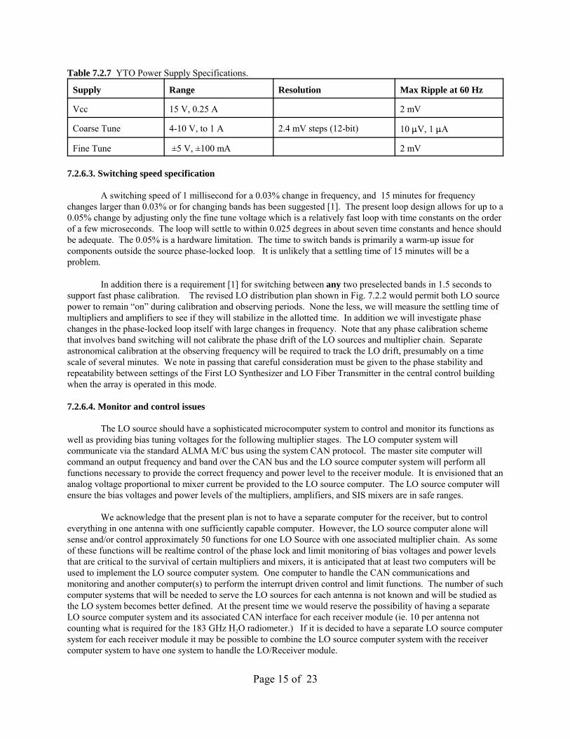
The goal for the phase noise from the YTO that is inside the loop bandwidth (from Table 7.2.6, YTODriver Inside) is 14 fs or 4µm. A level of 0.4 µm for the 60-Hz component was therefore chosen as an initial goalfor the 60 Hz contribution. Since the loop will provide less suppression for the second harmonic of the power mainsthese numbers should be a factor of 4 lower for the 120 Hz ripple frequencies. Some slight relaxing of thesespecifications may be possible for 50 Hz mains. The calculated values for ripple at 60 Hz agree with the observedvalues of 60 Hz phase noise as measured by the phase test system on the 80 GHz output, and the actual ripple on thecoarse tuning voltage as measured on the oscilloscope. Because the loop suppression is approximately -120 dB at100 Hz (going to 0 db at approx 100 kHz) but only -40 dB at 10 kHz, noise pickup from switching power supplies,which may have switching rates in the order of 10 kHz, is a serious concern. The YTO power supply specificationsare summarized in Table 7.2.7.
Note that the typical coarse tuning coil is 130 mH and 10 ohm series resistance, which is a one pole filterwith -3 dB cutoff at 12.2 Hz. The typical fine tuning coil is 1 ohm series resistance in the coil and 2µH with 50ohms in series from the driver circuit which gives a pole at 4 MHz. Shot and thermal noise are small for these coils.
Page 15 of 23
Table 7.2.7 YTO Power Supply Specifications.
Supply Range Resolution Max Ripple at 60 Hz
Vcc 15 V, 0.25 A 2 mV
Coarse Tune 4-10 V, to 1 A 2.4 mV steps (12-bit) 10 �V, 1 �A
Fine Tune ±5 V, ±100 mA 2 mV
7.2.6.3. Switching speed specification
A switching speed of 1 millisecond for a 0.03% change in frequency, and 15 minutes for frequencychanges larger than 0.03% or for changing bands has been suggested [1]. The present loop design allows for up to a0.05% change by adjusting only the fine tune voltage which is a relatively fast loop with time constants on the orderof a few microseconds. The loop will settle to within 0.025 degrees in about seven time constants and hence shouldbe adequate. The 0.05% is a hardware limitation. The time to switch bands is primarily a warm-up issue forcomponents outside the source phase-locked loop. It is unlikely that a settling time of 15 minutes will be aproblem.
In addition there is a requirement [1] for switching between any two preselected bands in 1.5 seconds tosupport fast phase calibration. The revised LO distribution plan shown in Fig. 7.2.2 would permit both LO sourcepower to remain �on� during calibration and observing periods. None the less, we will measure the settling time ofmultipliers and amplifiers to see if they will stabilize in the allotted time. In addition we will investigate phasechanges in the phase-locked loop itself with large changes in frequency. Note that any phase calibration schemethat involves band switching will not calibrate the phase drift of the LO sources and multiplier chain. Separateastronomical calibration at the observing frequency will be required to track the LO drift, presumably on a timescale of several minutes. We note in passing that careful consideration must be given to the phase stability andrepeatability between settings of the First LO Synthesizer and LO Fiber Transmitter in the central control buildingwhen the array is operated in this mode.
7.2.6.4. Monitor and control issues
The LO source should have a sophisticated microcomputer system to control and monitor its functions aswell as providing bias tuning voltages for the following multiplier stages. The LO computer system willcommunicate via the standard ALMA M/C bus using the system CAN protocol. The master site computer willcommand an output frequency and band over the CAN bus and the LO source computer system will perform allfunctions necessary to provide the correct frequency and power level to the receiver module. It is envisioned that ananalog voltage proportional to mixer current be provided to the LO source computer. The LO source computer willensure the bias voltages and power levels of the multipliers, amplifiers, and SIS mixers are in safe ranges.
We acknowledge that the present plan is not to have a separate computer for the receiver, but to controleverything in one antenna with one sufficiently capable computer. However, the LO source computer alone willsense and/or control approximately 50 functions for one LO Source with one associated multiplier chain. As someof these functions will be realtime control of the phase lock and limit monitoring of bias voltages and power levelsthat are critical to the survival of certain multipliers and mixers, it is anticipated that at least two computers will beused to implement the LO source computer system. One computer to handle the CAN communications andmonitoring and another computer(s) to perform the interrupt driven control and limit functions. The number of suchcomputer systems that will be needed to serve the LO sources for each antenna is not known and will be studied asthe LO system becomes better defined. At the present time we would reserve the possibility of having a separateLO source computer system and its associated CAN interface for each receiver module (ie. 10 per antenna notcounting what is required for the 183 GHz H2O radiometer.) If it is decided to have a separate LO source computersystem for each receiver module it may be possible to combine the LO source computer system with the receivercomputer system to have one system to handle the LO/Receiver module.
Page 16 of 23
The LO computer will be prototyped as per ALMA Computing Memo #7 [14] which states, �For benchtesting, the bus master will be a x86-based PC with LabView.� See reference 2 of [14] for details on the rationalebehind this design. The development and maintenance screens will be conducted in LabView, and then thealgorithms will be transferred to the prototype LO source computer during the Level-Two pre-production phase-locked source effort in the last half of 2001.
7.2.6.5. Spurious Outputs
Our current LO prototype may contain problematic spurious signals. We plan to work with the systemengineers to determine acceptable levels for spurious signals and to measure the spurious outputs of the Level Onepre-production source in the anechoic chamber located in Green Bank. At that point, appropriate remedies will beadministered as required.
7.2.7. List of Major Components
7.2.7.1. YTO and YTF
YTOs from MicroLambda have been shown to be adequate to meet the phase noise, amplitude noise, anddrift requirements of an LO source. An improved YTO that has been ruggedized for vibration will also be tested. We plan to procure for the Level-One source a YTF to do initial qualification in case such a filter is needed in thefinal design.
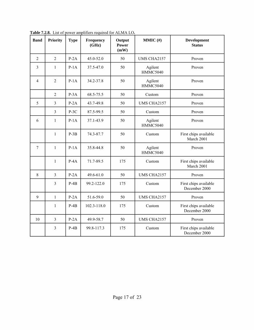
7.2.7.2. Power Amplifiers
Table 7.2.8 lists the power amplifiers required for the ALMA LO by band priority. P-1A and P-2A aresingle-MMIC amplifiers already demonstrated in our laboratory. Current work is concentrated on integration ofthese amplifiers with the multipliers inside the PLL. P-3A, P-3B, and P-3C will be single-MMIC amplifiers usingcustom-designed MMICs from either TRW or HRL. There is an ongoing collaboration with JPL on these customdevices. P-4A and P-4B use these same custom MMICs, but require power combining of either two or four devices.The development status of each amplifier is also given in Table 7.2.8.
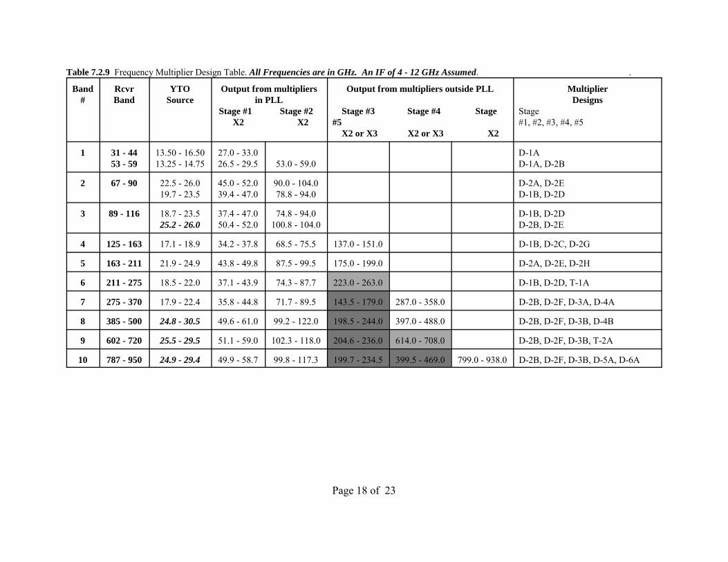
7.2.7.3. Multipliers
Table 7.2.9 shows a list of the frequency multipliers required for the ALMA LO sorted by receiver band. The lightly shaded boxes refer to tripler designs. The darker shaded boxes refer to doublers which must driverhigher frequency multipliers and consequently require a higher output power. Table 7.2.10 shows the same listsorted by multiplier topology. There are six basic doubler topologies and two basic tripler topologies. Multipliersof the same topology do not require separate development. The development status of each multiplier is given inTable 7.2.10.
7.2.7.4. Millimeter-wave isolators
Since frequency multipliers operate in a highly nonlinear state, impedance interactions between multiplierstages can result in large power variations over the operating band and phase changes. Ferrite isolators betweenstages can help reduce the severity of this effect. We are currently following the development of cryogenicwaveguide isolators by N. Erickson at FCRAO for the WR-5 (140-220 GHz) band. We plan to make use of theseisolators in our designs, and develop similar isolators for the WR-4 (170-260 GHz) band.
Page 17 of 23
Table 7.2.8. List of power amplifiers required for ALMA LO.
Band Priority Type Frequency(GHz)
OutputPower(mW)
MMIC (#) DevelopmentStatus
2 2 P-2A 45.0-52.0 50 UMS CHA2157 Proven
3 1 P-1A 37.5-47.0 50 AgilentHMMC5040
Proven
4 2 P-1A 34.2-37.8 50 AgilentHMMC5040
Proven
2 P-3A 68.5-75.5 50 Custom Proven
5 3 P-2A 43.7-49.8 50 UMS CHA2157 Proven
3 P-3C 87.5-99.5 50 Custom Proven
6 1 P-1A 37.1-43.9 50 AgilentHMMC5040
Proven
1 P-3B 74.3-87.7 50 Custom First chips availableMarch 2001
7 1 P-1A 35.8-44.8 50 AgilentHMMC5040
Proven
1 P-4A 71.7-89.5 175 Custom First chips availableMarch 2001
8 3 P-2A 49.6-61.0 50 UMS CHA2157 Proven
3 P-4B 99.2-122.0 175 Custom First chips availableDecember 2000
9 1 P-2A 51.6-59.0 50 UMS CHA2157 Proven
1 P-4B 102.3-118.0 175 Custom First chips availableDecember 2000
10 3 P-2A 49.9-58.7 50 UMS CHA2157 Proven
3 P-4B 99.8-117.3 175 Custom First chips availableDecember 2000
Page 18 of 23
Table 7.2.9 Frequency Multiplier Design Table. All Frequencies are in GHz. An IF of 4 - 12 GHz Assumed. .
Band#
RcvrBand
YTOSource
Output from multipliersin PLL
Stage #1 Stage #2 X2 X2
Output from multipliers outside PLL
Stage #3 Stage #4 Stage#5 X2 or X3 X2 or X3 X2
MultiplierDesigns
Stage#1, #2, #3, #4, #5
1 31 - 4453 - 59
13.50 - 16.5013.25 - 14.75
27.0 - 33.026.5 - 29.5 53.0 - 59.0
D-1AD-1A, D-2B
2 67 - 90 22.5 - 26.019.7 - 23.5
45.0 - 52.039.4 - 47.0
90.0 - 104.078.8 - 94.0
D-2A, D-2ED-1B, D-2D
3 89 - 116 18.7 - 23.525.2 - 26.0
37.4 - 47.050.4 - 52.0
74.8 - 94.0100.8 - 104.0
D-1B, D-2DD-2B, D-2E
4 125 - 163 17.1 - 18.9 34.2 - 37.8 68.5 - 75.5 137.0 - 151.0 D-1B, D-2C, D-2G
5 163 - 211 21.9 - 24.9 43.8 - 49.8 87.5 - 99.5 175.0 - 199.0 D-2A, D-2E, D-2H
6 211 - 275 18.5 - 22.0 37.1 - 43.9 74.3 - 87.7 223.0 - 263.0 D-1B, D-2D, T-1A
7 275 - 370 17.9 - 22.4 35.8 - 44.8 71.7 - 89.5 143.5 - 179.0 287.0 - 358.0 D-2B, D-2F, D-3A, D-4A
8 385 - 500 24.8 - 30.5 49.6 - 61.0 99.2 - 122.0 198.5 - 244.0 397.0 - 488.0 D-2B, D-2F, D-3B, D-4B
9 602 - 720 25.5 - 29.5 51.1 - 59.0 102.3 - 118.0 204.6 - 236.0 614.0 - 708.0 D-2B, D-2F, D-3B, T-2A
10 787 - 950 24.9 - 29.4 49.9 - 58.7 99.8 - 117.3 199.7 - 234.5 399.5 - 469.0 799.0 - 938.0 D-2B, D-2F, D-3B, D-5A, D-6A

Page 19 of 23
Table 7.2.10. Frequency multiplier list sorted by topology.
FrequencyMultipliers
Type Input Frequency
[GHz]
OutputFrequency
[GHz]
Bandwidth[Percent]
ReceiverPriority
DevelopmentStatus
D-1AD-1B
FET 13.25 - 16.517.0 - 23.5
26.5 - 33.034.0 - 47.0
2232
21,2
�Proven
D-2AD-2BD-2CD-2DD-2ED-2FD-2GD-2H
BalancedVaractor
(Discrete)
21.8 - 26.024.7 - 30.534.2 - 37.837.0 - 47.043.5 - 52.049.0 - 61.068.0 - 76.087.0 - 100.0
43.6 - 52.049.5 - 61.068.4 - 75.674.0 - 94.087.0 - 104.098.0 - 122.0136.0 - 152.0174.0 - 199.0
1821102418221113
2,31,2,3
21,2
1,2,31,323
�ProvenProvenProvenProvenProven
��
D-3AD-3B
High Power Varactor 71.7 - 89.599.0 - 122.0
143.5 - 179.0198.0 - 244.0
2221
11,3
Prototype completedPrototype evaluation underway
D-4AD-4B
Hybrid MMIC/Varistor 143.5 - 179.0198.5 - 244.0
287.0 - 358.0397.0 - 488.0
2221
13
Not Yet Designed�
D-5A High Power Varactor 199.7 - 234.5 399.5 - 469.0 16 3 �
D-6A Varistor 399.5 - 469.0 799.0 - 938.0 16 3 �
T-1A Hybrid MMIC/ Varactor 74.3 - 87.7 223.0 - 263.0 17 1 Designs underway
T-2A Varistor 204.7 - 236.0 614.0 - 708.0 14 1 Not yet designed
Page 20 of 23
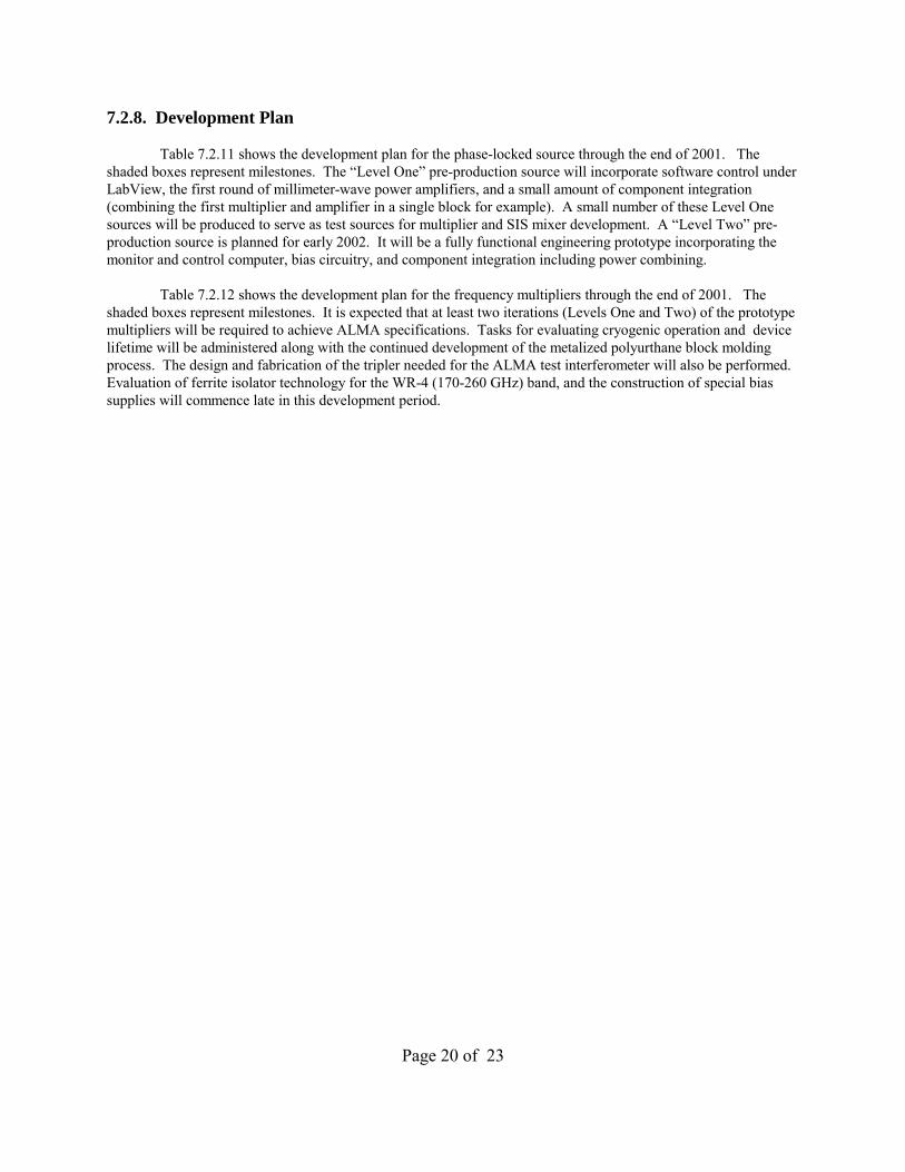
7.2.8. Development Plan
Table 7.2.11 shows the development plan for the phase-locked source through the end of 2001. Theshaded boxes represent milestones. The �Level One� pre-production source will incorporate software control underLabView, the first round of millimeter-wave power amplifiers, and a small amount of component integration(combining the first multiplier and amplifier in a single block for example). A small number of these Level Onesources will be produced to serve as test sources for multiplier and SIS mixer development. A �Level Two� pre-production source is planned for early 2002. It will be a fully functional engineering prototype incorporating themonitor and control computer, bias circuitry, and component integration including power combining.
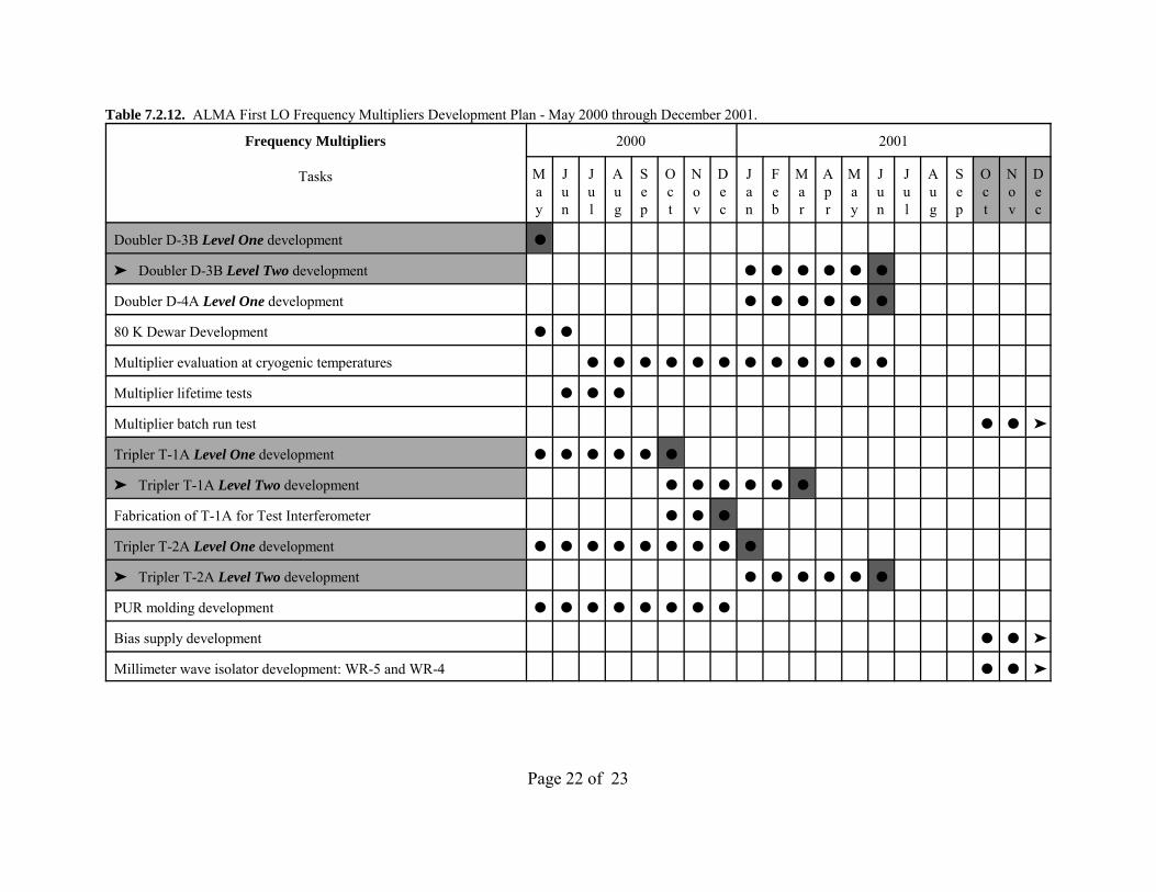
Table 7.2.12 shows the development plan for the frequency multipliers through the end of 2001. Theshaded boxes represent milestones. It is expected that at least two iterations (Levels One and Two) of the prototypemultipliers will be required to achieve ALMA specifications. Tasks for evaluating cryogenic operation and devicelifetime will be administered along with the continued development of the metalized polyurthane block moldingprocess. The design and fabrication of the tripler needed for the ALMA test interferometer will also be performed. Evaluation of ferrite isolator technology for the WR-4 (170-260 GHz) band, and the construction of special biassupplies will commence late in this development period.
Page 21 of 23
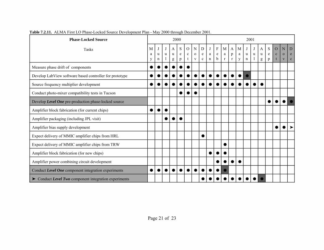
Table 7.2.11. ALMA First LO Phase-Locked Source Development Plan - May 2000 through December 2001.
Phase-Locked Source
Tasks
2000 2001
May
Jun
Jul
Aug
Sep
Oct
Nov
Dec
Jan
Feb
Mar
Apr
May
Jun
Jul
Aug
Sep
Oct
Nov
Dec
Measure phase drift of components � � � � � �
Develop LabView software based controller for prototype � � � � � � � � � � � � � �
Source frequency multiplier development � � � � � � � � � � � � � � � �
Conduct photo-mixer compatibility tests in Tucson � � �
Develop Level One pre-production phase-locked source � � � �
Amplifier block fabrication (for current chips) � � �
Amplifier packaging (including JPL visit) � � �
Amplifier bias supply development � � �
Expect delivery of MMIC amplifier chips from HRL �
Expect delivery of MMIC amplifier chips from TRW �
Amplifier block fabrication (for new chips) � � �
Amplifier power combining circuit development � � � �
Conduct Level One component integration experiments � � � � � � � � � � �
� Conduct Level Two component integration experiments � � � � � � � � �
Page 22 of 23
Table 7.2.12. ALMA First LO Frequency Multipliers Development Plan - May 2000 through December 2001.
Frequency Multipliers
Tasks
2000 2001
May
Jun
Jul
Aug
Sep
Oct
Nov
Dec
Jan
Feb
Mar
Apr
May
Jun
Jul
Aug
Sep
Oct
Nov
Dec
Doubler D-3B Level One development �
� Doubler D-3B Level Two development � � � � � �
Doubler D-4A Level One development � � � � � �
80 K Dewar Development � �
Multiplier evaluation at cryogenic temperatures � � � � � � � � � � � �
Multiplier lifetime tests � � �
Multiplier batch run test � � �
Tripler T-1A Level One development � � � � � �
� Tripler T-1A Level Two development � � � � � �
Fabrication of T-1A for Test Interferometer � � �
Tripler T-2A Level One development � � � � � � � � �
� Tripler T-2A Level Two development � � � � � �
PUR molding development � � � � � � � �
Bias supply development � � �
Millimeter wave isolator development: WR-5 and WR-4 � � �
Page 23 of 23
7.2.9. References
[1] L. D� Addario, �ALMA receivers, specifications adopted,� file: rcvrSpecs.txt, May 17, 2000. Currentlyavailable at http://www.tuc.nrao.edu/~ldaddari/rcvrSpecs.txt
[2] J. R. Tucker and M. J. Feldman, �Quantum detection at millimeter wavelengths,� Rev. of Modern Phys., vol. 4, pp. 1055-1113, 1985.
[3] A. R. Kerr and S-K. Pan, private communication.[4] ALMA Block Diagram: LO, Antenna Portion, File: alma.pdf, Feb. 21, 2000. Currently available at
http://www.tuc.nrao.edu/~ldaddari/alma.pdf[5] E. Bryerton, D.L. Thacker, K.S. Saini, and R.F. Bradley, �Noise Measurements of YIG Tuned Oscillator
Sources for the ALMA LO,� ALMA Memo # 311, (to be published shortly).[6] D.L. Thacker, E. Bryerton, K.S. Saini, and R.F. Bradley, �Drift Measurements of YIG Tuned Oscillator Sources
for the ALMA LO,� ALMA Memo #_______, (to be published shortly).[7] Private communication of 1992 data from A. R. Kerr and S. K. Pan.[8] R. Brown, �ALMA Science Requirements�, ALMA Project Book, Chapter 2. April 15, 2000 revision.[9] L. D�Addario, �ALMA Phase Stability Specification�Notes,� File: phaseSpecs.txt, Mar. 16, 2000. Currently
available at http://www.tuc.nrao.edu/~ldaddari/phaseSpecs.txt[10] Agilent Technologies, Test and Measurement Catalog 2000. [11] National Semiconductor, LM6171 Data Sheet, May, 1998. [12] P. Napier and J. West, �High Altitude Medical and Operations Problems and Solutions for the Millimeter
Array,� Proc. SPIE, 3349, 1998.[13] R. F. Bradley and R. J. Mattauch, �Planar monolithic Schottky varactor diode millimeter-wave frequency
multipliers,� Technical Report RL-TR-92-187, Rome Laboratory, Air Force Systems Command, GriffissAir Force Base, NY, June 1992.
[14] Mick Brooks, �ALMA Computing Memo 7 ALMA Monitor and Control Bus Interface Specification,� File:alma-sw-007.3.pdf, April 18, 2000. Currently available at http://www.mma.nrao.edu/development/computing/docs/memos/memo007/alma-sw-007.3.pdf