logic gates · practical # 01-verify ic 7432 for verifying or function apparatus 1- digital trainer...
TRANSCRIPT
2012 - 2013
Engr. ABDUL HAFEEZ
ELT LAB
LOGIC GATES
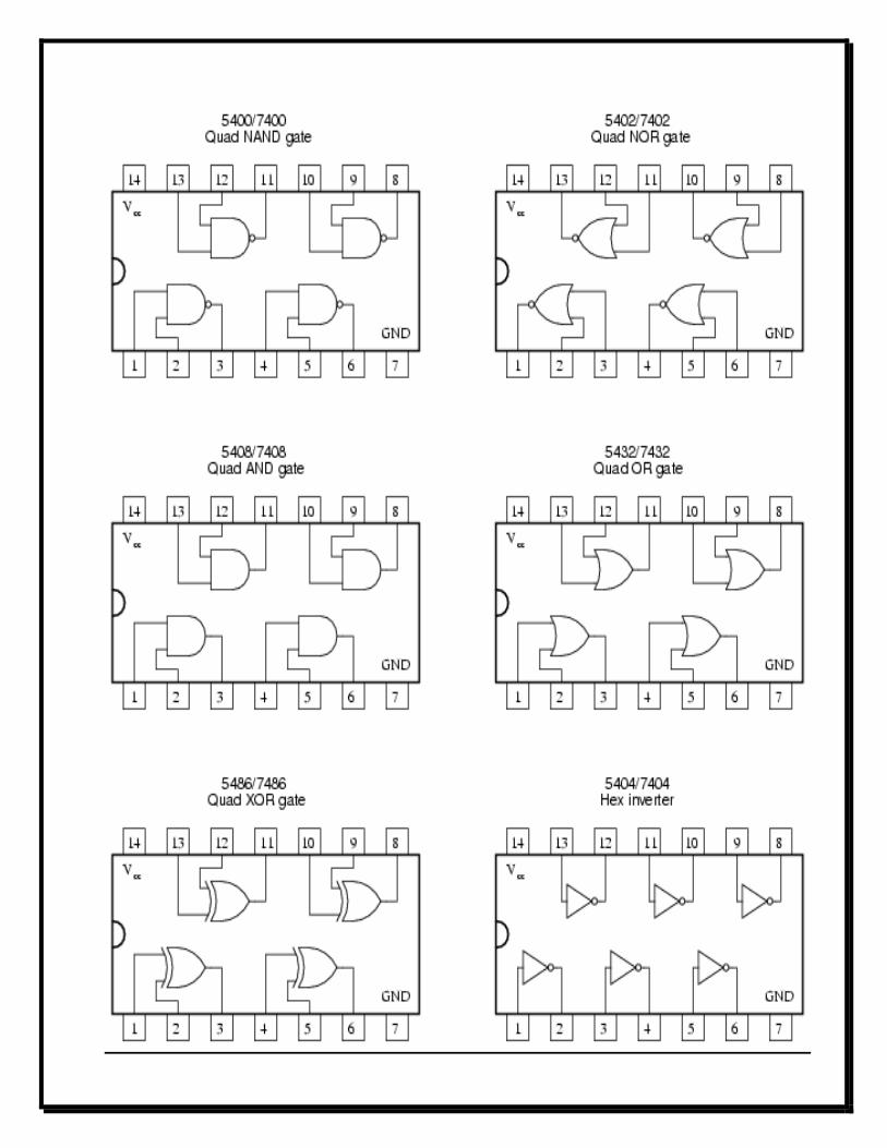
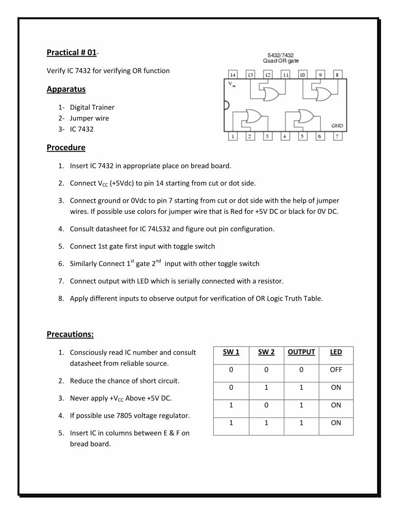
Practical # 01-
Verify IC 7432 for verifying OR function
Apparatus
1- Digital Trainer
2- Jumper wire
3- IC 7432
Procedure
1. Insert IC 7432 in appropriate place on bread board.
2. Connect VCC (+5Vdc) to pin 14 starting from cut or dot side.
3. Connect ground or 0Vdc to pin 7 starting from cut or dot side with the help of jumper
wires. If possible use colors for jumper wire that is Red for +5V DC or black for 0V DC.
4. Consult datasheet for IC 74LS32 and figure out pin configuration.
5. Connect 1st gate first input with toggle switch
6. Similarly Connect 1st gate 2nd input with other toggle switch
7. Connect output with LED which is serially connected with a resistor.
8. Apply different inputs to observe output for verification of OR Logic Truth Table.
Precautions:
1. Consciously read IC number and consult
datasheet from reliable source.
2. Reduce the chance of short circuit.
3. Never apply +VCC Above +5V DC.
4. If possible use 7805 voltage regulator.
5. Insert IC in columns between E & F on
bread board.
SW 1 SW 2 OUTPUT LED
0 0 0 OFF
0 1 1 ON
1 0 1 ON
1 1 1 ON
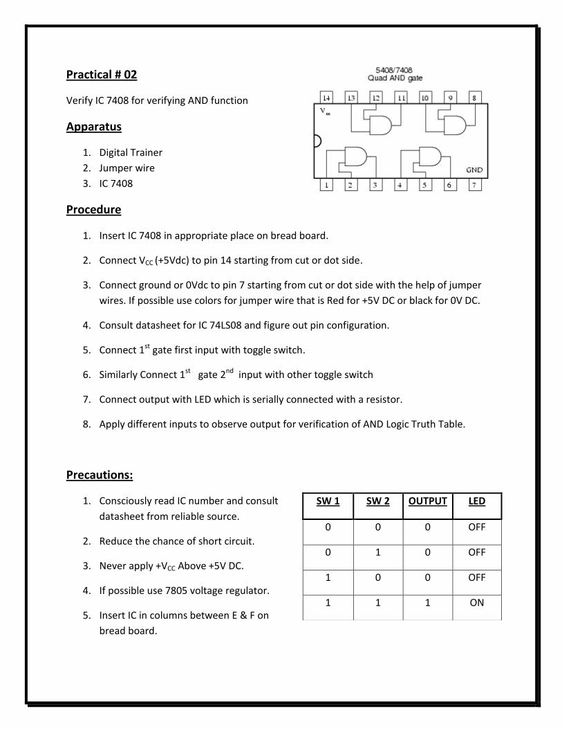
Practical # 02
Verify IC 7408 for verifying AND function
Apparatus
1. Digital Trainer
2. Jumper wire
3. IC 7408
Procedure
1. Insert IC 7408 in appropriate place on bread board.
2. Connect VCC (+5Vdc) to pin 14 starting from cut or dot side.
3. Connect ground or 0Vdc to pin 7 starting from cut or dot side with the help of jumper
wires. If possible use colors for jumper wire that is Red for +5V DC or black for 0V DC.
4. Consult datasheet for IC 74LS08 and figure out pin configuration.
5. Connect 1st gate first input with toggle switch.
6. Similarly Connect 1st gate 2nd input with other toggle switch
7. Connect output with LED which is serially connected with a resistor.
8. Apply different inputs to observe output for verification of AND Logic Truth Table.
Precautions:
1. Consciously read IC number and consult
datasheet from reliable source.
2. Reduce the chance of short circuit.
3. Never apply +VCC Above +5V DC.
4. If possible use 7805 voltage regulator.
5. Insert IC in columns between E & F on
bread board.
SW 1 SW 2 OUTPUT LED
0 0 0 OFF
0 1 0 OFF
1 0 0 OFF
1 1 1 ON
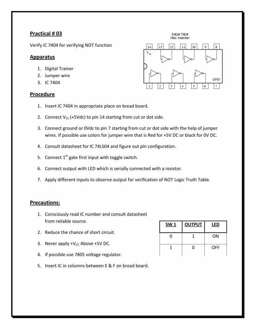
Practical # 03
Verify IC 7404 for verifying NOT function
Apparatus
1. Digital Trainer
2. Jumper wire
3. IC 7404
Procedure
1. Insert IC 7404 in appropriate place on bread board.
2. Connect VCC (+5Vdc) to pin 14 starting from cut or dot side.
3. Connect ground or 0Vdc to pin 7 starting from cut or dot side with the help of jumper
wires. If possible use colors for jumper wire that is Red for +5V DC or black for 0V DC.
4. Consult datasheet for IC 74LS04 and figure out pin configuration.
5. Connect 1st gate first input with toggle switch.
6. Connect output with LED which is serially connected with a resistor.
7. Apply different inputs to observe output for verification of NOT Logic Truth Table.
Precautions:
1. Consciously read IC number and consult datasheet
from reliable source.
2. Reduce the chance of short circuit.
3. Never apply +VCC Above +5V DC.
4. If possible use 7805 voltage regulator.
5. Insert IC in columns between E & F on bread board.
SW 1 OUTPUT LED
0 1 ON
1 0 OFF

Practical # 04
Verify IC 7400 for verifying NAND function
Apparatus
1. Digital Trainer
2. Jumper wire
3. IC 7400
Procedure
1. Insert IC 7400 in appropriate place on bread board.
2. Connect VCC (+5Vdc) to pin 14 starting from cut or dot side.
3. Connect ground or 0Vdc to pin 7 starting from cut or dot side with the help of jumper
wires. If possible use colors for jumper wire that is Red for +5V DC or black for 0V DC.
4. Consult datasheet for IC 74LS00 and figure out pin configuration.
5. Connect 1st gate first input with toggle switch.
6. Similarly Connect 1st gate 2nd input with other toggle switch.
7. Connect output with LED which is serially connected with a resistor.
8. Apply different inputs to observe output for verification of NAND Logic Truth Table.
Precautions:
1. Consciously read IC number and consult
datasheet from reliable source.
2. Reduce the chance of short circuit.
3. Never apply +VCC Above +5V DC.
4. If possible use 7805 voltage regulator.
5. Insert IC in columns between E & F on
bread board.
SW 1 SW 2 OUTPUT LED
0 0 1 ON
0 1 1 ON
1 0 1 ON
1 1 0 OFF

Practical # 05
Verify IC 7402 for verifying NOR function
Apparatus
1. Digital Trainer
2. Jumper wire
3. IC 7402
Procedure
1. Insert IC 7402 in appropriate place on bread board.
2. Connect VCC (+5Vdc) to pin 14 starting from cut or dot side.
3. Connect ground or 0Vdc to pin 7 starting from cut or dot side with the help of jumper
wires. If possible use colors for jumper wire that is Red for +5V DC or black for 0V DC.
4. Consult datasheet for IC 74LS02 and figure out pin configuration.
5. Connect 1st gate first input with toggle switch.
6. Similarly Connect 1st gate 2nd input with other toggle switch
7. Connect output with LED which is serially connected with a resistor.
8. Apply different inputs to observe output for verification of NOR Logic Truth Table.
Precautions:
1. Consciously read IC number and consult
datasheet from reliable source.
2. Reduce the chance of short circuit.
3. Never apply +VCC Above +5V DC.
4. If possible use 7805 voltage regulator.
5. Insert IC in columns between E & F on
bread board.
SW 1 SW 2 OUTPUT LED
0 0 1 ON
0 1 0 OFF
1 0 0 OFF
1 1 0 OFF
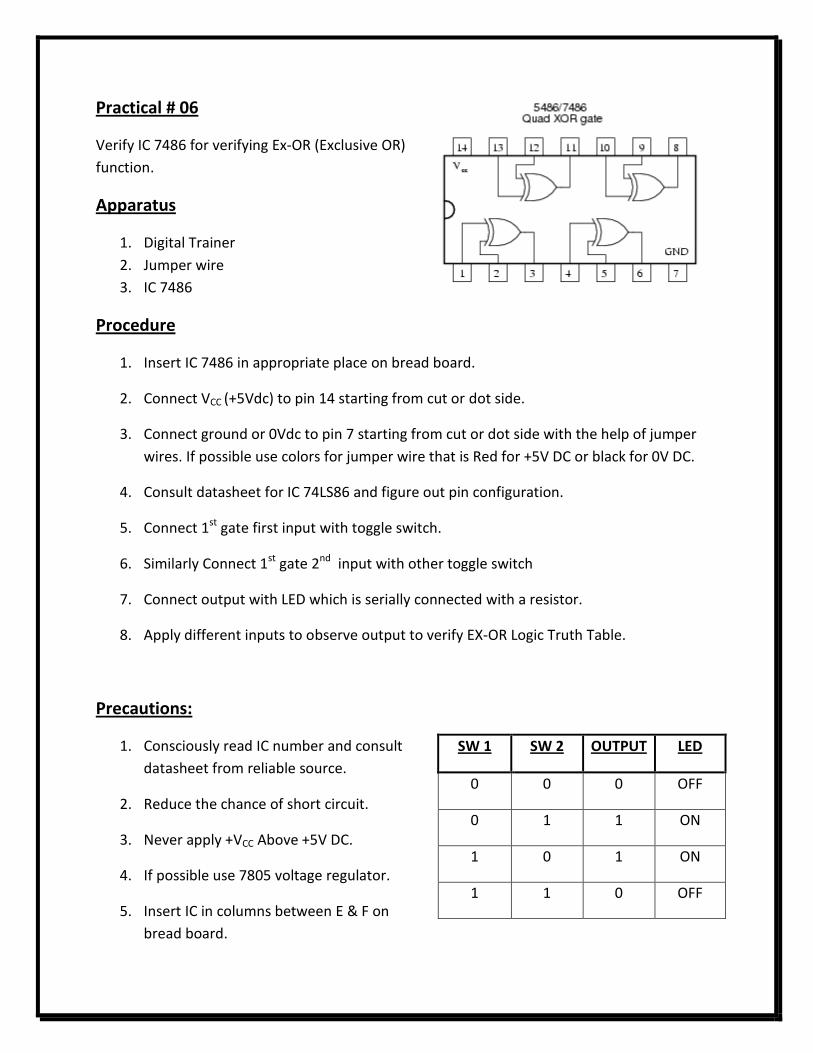
Practical # 06
Verify IC 7486 for verifying Ex-OR (Exclusive OR)
function.
Apparatus
1. Digital Trainer
2. Jumper wire
3. IC 7486
Procedure
1. Insert IC 7486 in appropriate place on bread board.
2. Connect VCC (+5Vdc) to pin 14 starting from cut or dot side.
3. Connect ground or 0Vdc to pin 7 starting from cut or dot side with the help of jumper
wires. If possible use colors for jumper wire that is Red for +5V DC or black for 0V DC.
4. Consult datasheet for IC 74LS86 and figure out pin configuration.
5. Connect 1st gate first input with toggle switch.
6. Similarly Connect 1st gate 2nd input with other toggle switch
7. Connect output with LED which is serially connected with a resistor.
8. Apply different inputs to observe output to verify EX-OR Logic Truth Table.
Precautions:
1. Consciously read IC number and consult
datasheet from reliable source.
2. Reduce the chance of short circuit.
3. Never apply +VCC Above +5V DC.
4. If possible use 7805 voltage regulator.
5. Insert IC in columns between E & F on
bread board.
SW 1 SW 2 OUTPUT LED
0 0 0 OFF
0 1 1 ON
1 0 1 ON
1 1 0 OFF
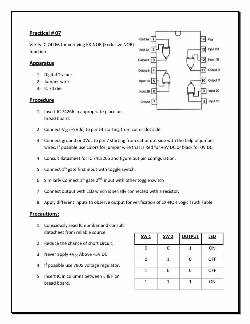
Practical # 07
Verify IC 74266 for verifying EX-NOR (Exclusive NOR)
function.
Apparatus
1- Digital Trainer
2- Jumper wire
3- IC 74266
Procedure
1. Insert IC 74266 in appropriate place on
bread board.
2. Connect VCC (+5Vdc) to pin 14 starting from cut or dot side.
3. Connect ground or 0Vdc to pin 7 starting from cut or dot side with the help of jumper
wires. If possible use colors for jumper wire that is Red for +5V DC or black for 0V DC.
4. Consult datasheet for IC 74LS266 and figure out pin configuration.
5. Connect 1st gate first input with toggle switch.
6. Similarly Connect 1st gate 2nd input with other toggle switch
7. Connect output with LED which is serially connected with a resistor.
8. Apply different inputs to observe output for verification of EX-NOR Logic Truth Table.
Precautions:
1. Consciously read IC number and consult
datasheet from reliable source.
2. Reduce the chance of short circuit.
3. Never apply +VCC Above +5V DC.
4. If possible use 7805 voltage regulator.
5. Insert IC in columns between E & F on
bread board.
SW 1 SW 2 OUTPUT LED
0 0 1 ON
0 1 0 OFF
1 0 0 OFF
1 1 1 ON
Practical # 08
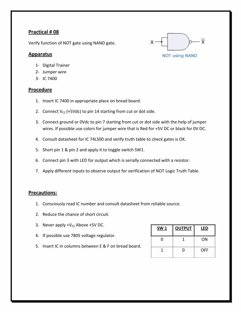
Verify function of NOT gate using NAND gate.
Apparatus
1- Digital Trainer
2- Jumper wire
3- IC 7400
Procedure
1. Insert IC 7400 in appropriate place on bread board.
2. Connect VCC (+5Vdc) to pin 14 starting from cut or dot side.
3. Connect ground or 0Vdc to pin 7 starting from cut or dot side with the help of jumper
wires. If possible use colors for jumper wire that is Red for +5V DC or black for 0V DC.
4. Consult datasheet for IC 74LS00 and verify truth table to check gates is OK.
5. Short pin 1 & pin 2 and apply it to toggle switch SW1.
6. Connect pin 3 with LED for output which is serially connected with a resistor.
7. Apply different inputs to observe output for verification of NOT Logic Truth Table.
Precautions:
1. Consciously read IC number and consult datasheet from reliable source.
2. Reduce the chance of short circuit.
3. Never apply +VCC Above +5V DC.
4. If possible use 7805 voltage regulator.
5. Insert IC in columns between E & F on bread board.
SW 1 OUTPUT LED
0 1 ON
1 0 OFF
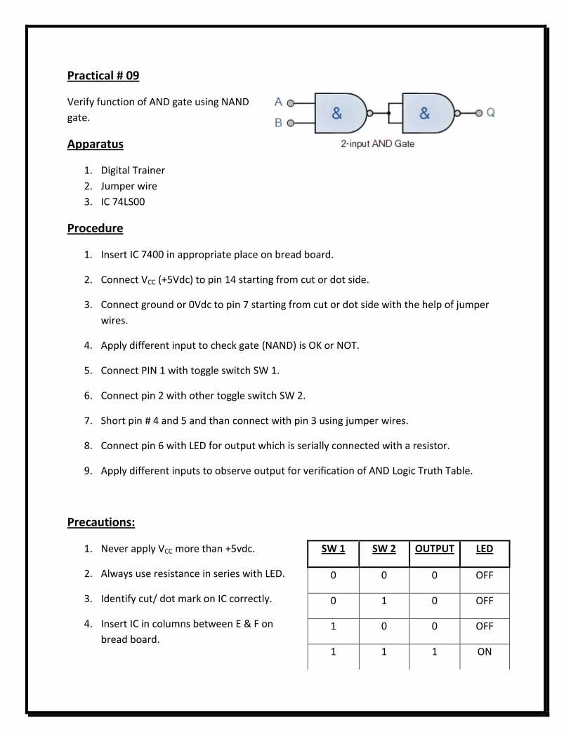
Practical # 09
Verify function of AND gate using NAND
gate.
Apparatus
1. Digital Trainer
2. Jumper wire
3. IC 74LS00
Procedure
1. Insert IC 7400 in appropriate place on bread board.
2. Connect VCC (+5Vdc) to pin 14 starting from cut or dot side.
3. Connect ground or 0Vdc to pin 7 starting from cut or dot side with the help of jumper
wires.
4. Apply different input to check gate (NAND) is OK or NOT.
5. Connect PIN 1 with toggle switch SW 1.
6. Connect pin 2 with other toggle switch SW 2.
7. Short pin # 4 and 5 and than connect with pin 3 using jumper wires.
8. Connect pin 6 with LED for output which is serially connected with a resistor.
9. Apply different inputs to observe output for verification of AND Logic Truth Table.
Precautions:
1. Never apply VCC more than +5vdc.
2. Always use resistance in series with LED.
3. Identify cut/ dot mark on IC correctly.
4. Insert IC in columns between E & F on
bread board.
SW 1 SW 2 OUTPUT LED
0 0 0 OFF
0 1 0 OFF
1 0 0 OFF
1 1 1 ON
Practical # 10
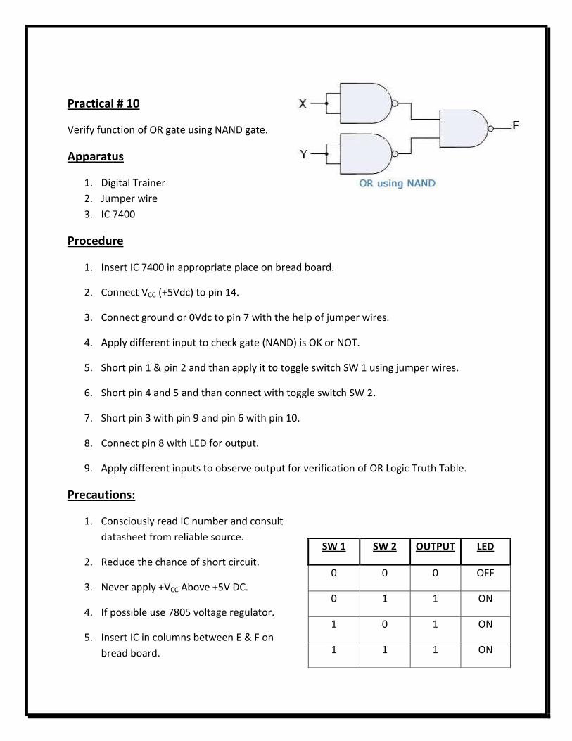
Verify function of OR gate using NAND gate.
Apparatus
1. Digital Trainer
2. Jumper wire
3. IC 7400
Procedure
1. Insert IC 7400 in appropriate place on bread board.
2. Connect VCC (+5Vdc) to pin 14.
3. Connect ground or 0Vdc to pin 7 with the help of jumper wires.
4. Apply different input to check gate (NAND) is OK or NOT.
5. Short pin 1 & pin 2 and than apply it to toggle switch SW 1 using jumper wires.
6. Short pin 4 and 5 and than connect with toggle switch SW 2.
7. Short pin 3 with pin 9 and pin 6 with pin 10.
8. Connect pin 8 with LED for output.
9. Apply different inputs to observe output for verification of OR Logic Truth Table.
Precautions:
1. Consciously read IC number and consult
datasheet from reliable source.
2. Reduce the chance of short circuit.
3. Never apply +VCC Above +5V DC.
4. If possible use 7805 voltage regulator.
5. Insert IC in columns between E & F on
bread board.
SW 1 SW 2 OUTPUT LED
0 0 0 OFF
0 1 1 ON
1 0 1 ON
1 1 1 ON
Practical # 11
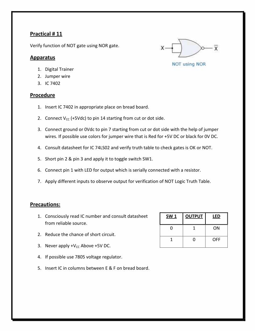
Verify function of NOT gate using NOR gate.
Apparatus
1. Digital Trainer
2. Jumper wire
3. IC 7402
Procedure
1. Insert IC 7402 in appropriate place on bread board.
2. Connect VCC (+5Vdc) to pin 14 starting from cut or dot side.
3. Connect ground or 0Vdc to pin 7 starting from cut or dot side with the help of jumper
wires. If possible use colors for jumper wire that is Red for +5V DC or black for 0V DC.
4. Consult datasheet for IC 74LS02 and verify truth table to check gates is OK or NOT.
5. Short pin 2 & pin 3 and apply it to toggle switch SW1.
6. Connect pin 1 with LED for output which is serially connected with a resistor.
7. Apply different inputs to observe output for verification of NOT Logic Truth Table.
Precautions:
1. Consciously read IC number and consult datasheet
from reliable source.
2. Reduce the chance of short circuit.
3. Never apply +VCC Above +5V DC.
4. If possible use 7805 voltage regulator.
5. Insert IC in columns between E & F on bread board.
SW 1 OUTPUT LED
0 1 ON
1 0 OFF
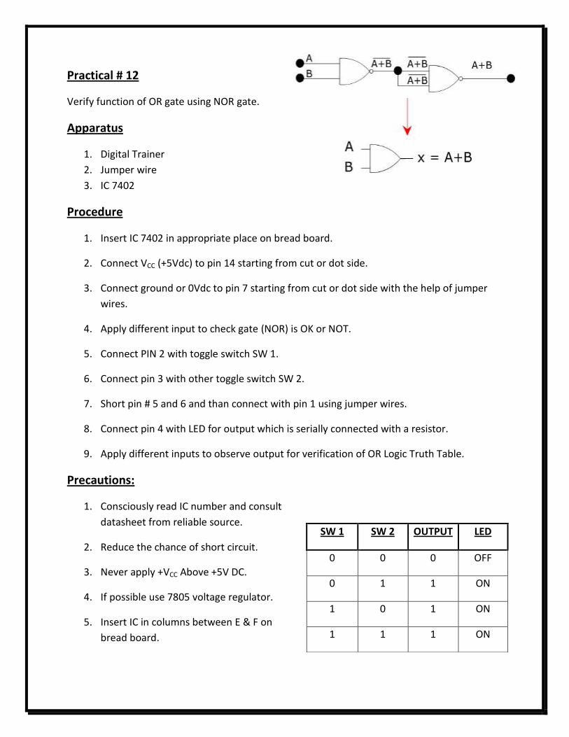
Practical # 12
Verify function of OR gate using NOR gate.
Apparatus
1. Digital Trainer
2. Jumper wire
3. IC 7402
Procedure
1. Insert IC 7402 in appropriate place on bread board.
2. Connect VCC (+5Vdc) to pin 14 starting from cut or dot side.
3. Connect ground or 0Vdc to pin 7 starting from cut or dot side with the help of jumper
wires.
4. Apply different input to check gate (NOR) is OK or NOT.
5. Connect PIN 2 with toggle switch SW 1.
6. Connect pin 3 with other toggle switch SW 2.
7. Short pin # 5 and 6 and than connect with pin 1 using jumper wires.
8. Connect pin 4 with LED for output which is serially connected with a resistor.
9. Apply different inputs to observe output for verification of OR Logic Truth Table.
Precautions:
1. Consciously read IC number and consult
datasheet from reliable source.
2. Reduce the chance of short circuit.
3. Never apply +VCC Above +5V DC.
4. If possible use 7805 voltage regulator.
5. Insert IC in columns between E & F on
bread board.
SW 1 SW 2 OUTPUT LED
0 0 0 OFF
0 1 1 ON
1 0 1 ON
1 1 1 ON
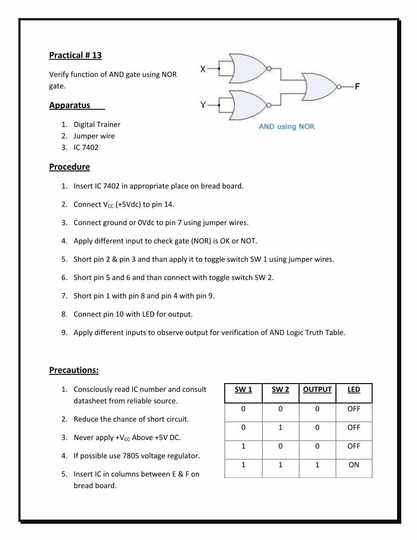
Practical # 13
Verify function of AND gate using NOR
gate.
Apparatus
1. Digital Trainer
2. Jumper wire
3. IC 7402
Procedure
1. Insert IC 7402 in appropriate place on bread board.
2. Connect VCC (+5Vdc) to pin 14.
3. Connect ground or 0Vdc to pin 7 using jumper wires.
4. Apply different input to check gate (NOR) is OK or NOT.
5. Short pin 2 & pin 3 and than apply it to toggle switch SW 1 using jumper wires.
6. Short pin 5 and 6 and than connect with toggle switch SW 2.
7. Short pin 1 with pin 8 and pin 4 with pin 9.
8. Connect pin 10 with LED for output.
9. Apply different inputs to observe output for verification of AND Logic Truth Table.
Precautions:
1. Consciously read IC number and consult
datasheet from reliable source.
2. Reduce the chance of short circuit.
3. Never apply +VCC Above +5V DC.
4. If possible use 7805 voltage regulator.
5. Insert IC in columns between E & F on
bread board.
SW 1 SW 2 OUTPUT LED
0 0 0 OFF
0 1 0 OFF
1 0 0 OFF
1 1 1 ON
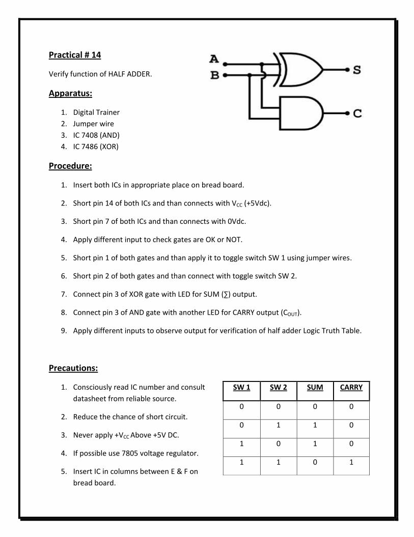
Practical # 14
Verify function of HALF ADDER.
Apparatus:
1. Digital Trainer
2. Jumper wire
3. IC 7408 (AND)
4. IC 7486 (XOR)
Procedure:
1. Insert both ICs in appropriate place on bread board.
2. Short pin 14 of both ICs and than connects with VCC (+5Vdc).
3. Short pin 7 of both ICs and than connects with 0Vdc.
4. Apply different input to check gates are OK or NOT.
5. Short pin 1 of both gates and than apply it to toggle switch SW 1 using jumper wires.
6. Short pin 2 of both gates and than connect with toggle switch SW 2.
7. Connect pin 3 of XOR gate with LED for SUM (∑) output.
8. Connect pin 3 of AND gate with another LED for CARRY output (COUT).
9. Apply different inputs to observe output for verification of half adder Logic Truth Table.
Precautions:
1. Consciously read IC number and consult
datasheet from reliable source.
2. Reduce the chance of short circuit.
3. Never apply +VCC Above +5V DC.
4. If possible use 7805 voltage regulator.
5. Insert IC in columns between E & F on
bread board.
SW 1 SW 2 SUM CARRY
0 0 0 0
0 1 1 0
1 0 1 0
1 1 0 1
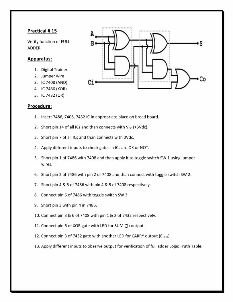
Practical # 15
Verify function of FULL
ADDER.
Apparatus:
1. Digital Trainer
2. Jumper wire
3. IC 7408 (AND)
4. IC 7486 (XOR)
5. IC 7432 (OR)
Procedure:
1. Insert 7486, 7408, 7432 IC in appropriate place on bread board.
2. Short pin 14 of all ICs and than connects with VCC (+5Vdc).
3. Short pin 7 of all ICs and than connects with 0Vdc.
4. Apply different inputs to check gates in ICs are OK or NOT.
5. Short pin 1 of 7486 with 7408 and than apply it to toggle switch SW 1 using jumper
wires.
6. Short pin 2 of 7486 with pin 2 of 7408 and than connect with toggle switch SW 2.
7. Short pin 4 & 5 of 7486 with pin 4 & 5 of 7408 respectively.
8. Connect pin 6 of 7486 with toggle switch SW 3.
9. Short pin 3 with pin 4 in 7486.
10. Connect pin 3 & 6 of 7408 with pin 1 & 2 of 7432 respectively.
11. Connect pin 6 of XOR gate with LED for SUM (∑) output.
12. Connect pin 3 of 7432 gate with another LED for CARRY output (COUT).
13. Apply different inputs to observe output for verification of full adder Logic Truth Table.
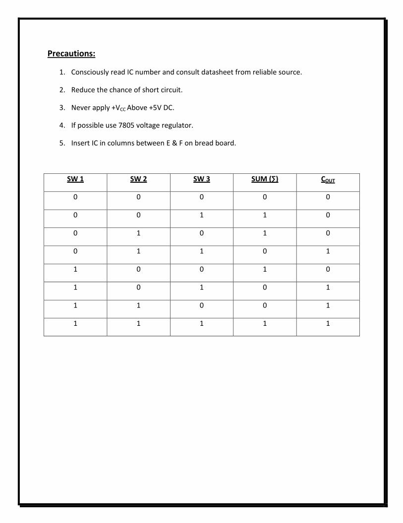
Precautions:
1. Consciously read IC number and consult datasheet from reliable source.
2. Reduce the chance of short circuit.
3. Never apply +VCC Above +5V DC.
4. If possible use 7805 voltage regulator.
5. Insert IC in columns between E & F on bread board.
SW 1 SW 2 SW 3 SUM (∑) COUT
0 0 0 0 0
0 0 1 1 0
0 1 0 1 0
0 1 1 0 1
1 0 0 1 0
1 0 1 0 1
1 1 0 0 1
1 1 1 1 1
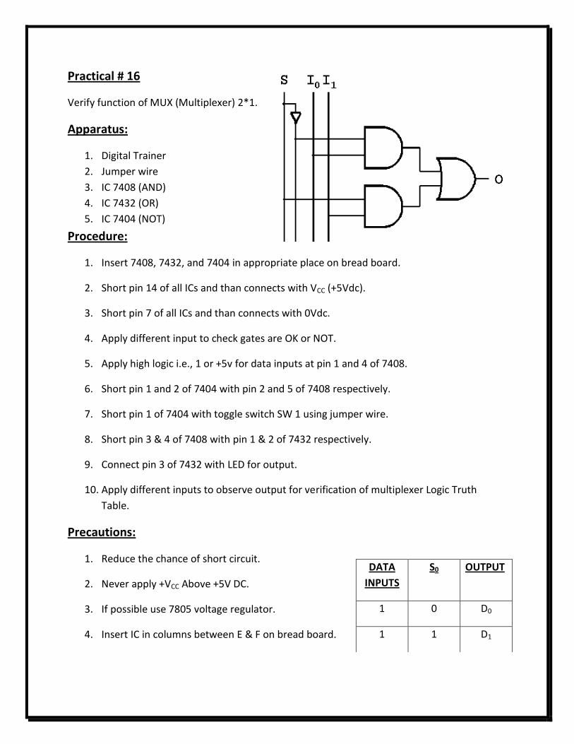
Practical # 16
Verify function of MUX (Multiplexer) 2*1.
Apparatus:
1. Digital Trainer
2. Jumper wire
3. IC 7408 (AND)
4. IC 7432 (OR)
5. IC 7404 (NOT)
Procedure:
1. Insert 7408, 7432, and 7404 in appropriate place on bread board.
2. Short pin 14 of all ICs and than connects with VCC (+5Vdc).
3. Short pin 7 of all ICs and than connects with 0Vdc.
4. Apply different input to check gates are OK or NOT.
5. Apply high logic i.e., 1 or +5v for data inputs at pin 1 and 4 of 7408.
6. Short pin 1 and 2 of 7404 with pin 2 and 5 of 7408 respectively.
7. Short pin 1 of 7404 with toggle switch SW 1 using jumper wire.
8. Short pin 3 & 4 of 7408 with pin 1 & 2 of 7432 respectively.
9. Connect pin 3 of 7432 with LED for output.
10. Apply different inputs to observe output for verification of multiplexer Logic Truth
Table.
Precautions:
1. Reduce the chance of short circuit.
2. Never apply +VCC Above +5V DC.
3. If possible use 7805 voltage regulator.
4. Insert IC in columns between E & F on bread board.
DATA
INPUTS
S0 OUTPUT
1 0 D0
1 1 D1
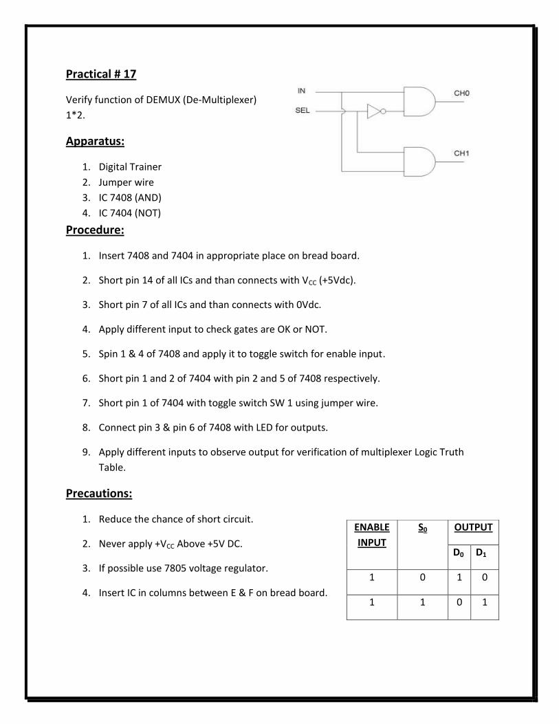
Practical # 17
Verify function of DEMUX (De-Multiplexer)
1*2.
Apparatus:
1. Digital Trainer
2. Jumper wire
3. IC 7408 (AND)
4. IC 7404 (NOT)
Procedure:
1. Insert 7408 and 7404 in appropriate place on bread board.
2. Short pin 14 of all ICs and than connects with VCC (+5Vdc).
3. Short pin 7 of all ICs and than connects with 0Vdc.
4. Apply different input to check gates are OK or NOT.
5. Spin 1 & 4 of 7408 and apply it to toggle switch for enable input.
6. Short pin 1 and 2 of 7404 with pin 2 and 5 of 7408 respectively.
7. Short pin 1 of 7404 with toggle switch SW 1 using jumper wire.
8. Connect pin 3 & pin 6 of 7408 with LED for outputs.
9. Apply different inputs to observe output for verification of multiplexer Logic Truth
Table.
Precautions:
1. Reduce the chance of short circuit.
2. Never apply +VCC Above +5V DC.
3. If possible use 7805 voltage regulator.
4. Insert IC in columns between E & F on bread board.
ENABLE
INPUT
S0 OUTPUT
D0 D1
1 0 1 0
1 1 0 1
Practical # 18
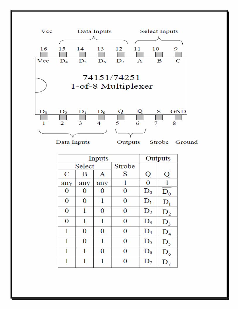
Verify function of MUX (Multiplexer) 8*1 Using IC 74151.
Apparatus:
1. Digital Trainer
2. Jumper wire
3. IC 74151
Procedure:
1. Insert 74151 in appropriate place on bread board.
2. Connect pin 16 of IC with VCC (+5Vdc).
3. Short pin 7 (strobe pin) with pin 8 of 74151 than connect it with 0vdc.
4. Read the data sheet of 74151 for pin configuration of IC.
5. Connect pin 1 – 4 & from pin 11 - 15 with toggle switches and apply high logics on it.
6. Connect pin 5 & 6 with LED’s for output.
7. Connect pin 9, 10 & 11 with toggle switches SW1, SW2 & SW3 respectively for selection
lines.
8. Apply different inputs to observe output for verification of multiplexer Truth Table.
Precautions:
1. Reduce the chance of short circuit.
2. Never apply +VCC Above +5V DC.
3. If possible use 7805 voltage regulator.
4. Insert IC in columns between E & F on bread board.
Practical # 19
Verify function of DE-MUX (Multiplexer) 1*8 Using IC 74138.
Apparatus:
1. Digital Trainer
2. Jumper wire
3. IC 74151
Procedure:
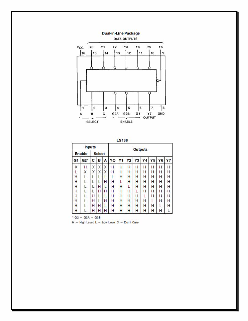
1. Insert 74138 in appropriate place on bread board.
2. Read the data sheet of 74138 for pin configuration of IC.
3. Short pin 6 with pin 16 of IC 74138 & connect it with VCC (+5Vdc).
4. Short pin 4, 5 (EN pin) with pin 8 of 74138 than connect it with 0vdc.
5. Connect pin 9-15 & 6 with LED’s for data outputs.
6. Connect pin 1, 2 & 3 with toggle switches SW1, SW2 & SW3 respectively for selection
lines.
7. Apply different inputs to observe output for verification of de - multiplexer Truth Table.
Precautions:
1. Reduce the chance of short circuit.
2. Never apply +VCC Above +5V DC.
3. If possible use 7805 voltage regulator.
4. Insert IC in columns between E & F on bread board.
Practical # 20
Verify function of ENCODER (Decimal to binary converter) 4*2.
Apparatus:
1. Digital Trainer
2. Jumper wire
3. IC 7432 (OR)
Procedure:
1. Insert IC 7432 in appropriate place on bread board.
2. Connect VCC (+5Vdc) to pin 14 starting from cut or dot side.
3. Connect ground or 0Vdc to pin 7 starting from cut or dot side with the help of jumper
wire.
4. Apply different input to check gate (OR) is OK or NOT.
5. For decimal no. 0 no connection made with gates.
6. For decimal 1, connect toggle switch SW2 with pin 1.
7. For decimal 2, connect toggle switch SW3 with pin 4.
8. For decimal 3, connect toggle switch SW4 with pin 2 & 5 of IC.
9. Connect pin 3 & pin 6 with LED’s which shows binary code of decimal input.
10. The 1ST gate o/p is considered as “A” and the 2nd gate o/p is considered as “B”.
11. Apply different inputs to observe output for verification of encoder Truth Table.
Precautions:
1. Reduce the chance of short circuit.
2. Never apply +VCC Above +5V DC.
3. Insert IC in columns between E & F on bread board.
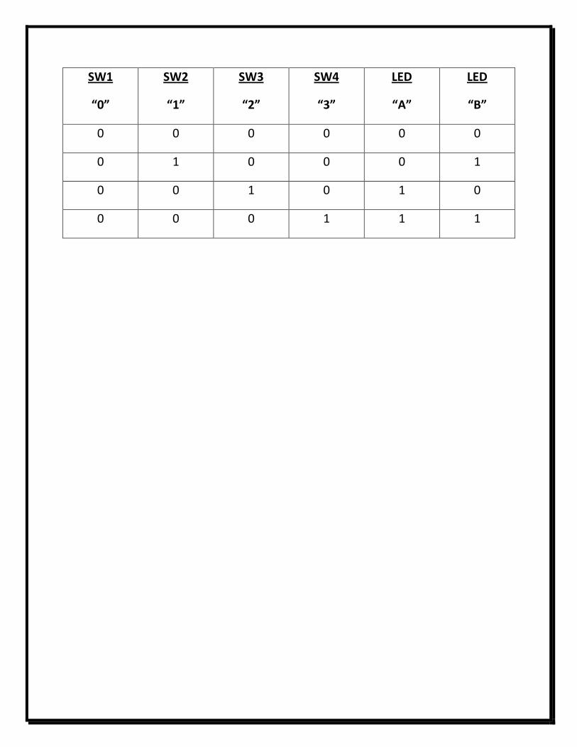
SW1
“0”
SW2
“1”
SW3
“2”
SW4
“3”
LED
“A”
LED
“B”
0 0 0 0 0 0
0 1 0 0 0 1
0 0 1 0 1 0
0 0 0 1 1 1
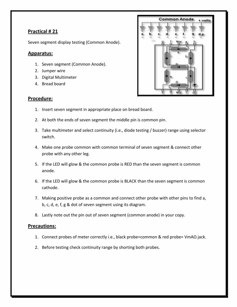
Practical # 21
Seven segment display testing (Common Anode).
Apparatus:
1. Seven segment (Common Anode).
2. Jumper wire
3. Digital Multimeter
4. Bread board
Procedure:
1. Insert seven segment in appropriate place on bread board.
2. At both the ends of seven segment the middle pin is common pin.
3. Take multimeter and select continuity (i.e., diode testing / buzzer) range using selector
switch.
4. Make one probe common with common terminal of seven segment & connect other
probe with any other leg.
5. If the LED will glow & the common probe is RED than the seven segment is common
anode.
6. If the LED will glow & the common probe is BLACK than the seven segment is common
cathode.
7. Making positive probe as a common and connect other probe with other pins to find a,
b, c, d, e, f, g & dot of seven segment using its diagram.
8. Lastly note out the pin out of seven segment (common anode) in your copy.
Precautions:
1. Connect probes of meter correctly i.e., black probe=common & red probe= VmAΩ jack.
2. Before testing check continuity range by shorting both probes.
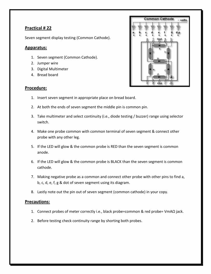
Practical # 22
Seven segment display testing (Common Cathode).
Apparatus:
1. Seven segment (Common Cathode).
2. Jumper wire
3. Digital Multimeter
4. Bread board
Procedure:
1. Insert seven segment in appropriate place on bread board.
2. At both the ends of seven segment the middle pin is common pin.
3. Take multimeter and select continuity (i.e., diode testing / buzzer) range using selector
switch.
4. Make one probe common with common terminal of seven segment & connect other
probe with any other leg.
5. If the LED will glow & the common probe is RED than the seven segment is common
anode.
6. If the LED will glow & the common probe is BLACK than the seven segment is common
cathode.
7. Making negative probe as a common and connect other probe with other pins to find a,
b, c, d, e, f, g & dot of seven segment using its diagram.
8. Lastly note out the pin out of seven segment (common cathode) in your copy.
Precautions:
1. Connect probes of meter correctly i.e., black probe=common & red probe= VmAΩ jack.
2. Before testing check continuity range by shorting both probes.
Practical # 23
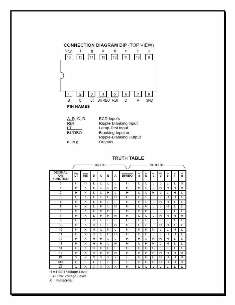
Verify function of DCD to 7 segment decoder/driver.
Apparatus:
1. Digital Trainer
2. Jumper wire
3. IC 7447
4. 7 segment (Common Anode)
Procedure:
1. Insert IC 7447 in appropriate place on bread board.
2. Connect VCC (+5Vdc) to pin 16 starting from cut or dot side.
3. Connect ground or 0Vdc to pin 8 starting from cut or dot side with the help of jumper
wire.
4. Consult datasheet of 7447 for its pin out.
5. Connect pin 9 – 15 i.e., a – g with 7 segment respectively.
6. Connect pin 1,2,6,7 with toggle switches SW1, SW2, SW3 & SW4 respectively.
7. For decimal 3, connect toggle switch SW4 with pin 2 & 5 of IC.
8. Connect pin 3 & pin 6 with LED’s which shows binary code of decimal input.
9. The 1ST gate o/p is considered as “A” and the 2nd gate o/p is considered as “B”.
10. Apply different inputs to observe output for verification of encoder Truth Table.
Precautions:
1. Reduce the chance of short circuit.
2. Never apply +VCC Above +5V DC.
3. Insert IC in columns between E & F on bread board.