low dark current p-on-n technology for space applications · the applications envisioned with this...
TRANSCRIPT
Low dark current P-on-N technology for space applications
www.sofradir-ec.com
Access to the world’s leading infrared imaging technology

Low dark current p-on-n technology for space applications
N. Péré-Lapernea, N. Baier
b, C. Cervera
b, J.L. Santailler
b, C. Lobre
b, C. Cassillo
a, J. Berthoz
a, V.
Destefanisa, D. Sam Giao
a, A. Lamoure
a
aSOFRADIR, avenue de Vauve - CS20018, 91127 Palaiseau, France;
bUniv. Grenoble Alpes, CEA-
LETI, MINATEC Campus, 38054 Grenoble, France
ABSTRACT
Space applications are requiring low dark current in the long wave infrared at low operating temperature for low flux
observation. The applications envisioned with this type of specification are namely scientific and planetary missions.
Within the framework of the joint laboratory between Sofradir and the CEA-LETI, a specific development of a TV
format focal plane array with a cut-off wavelength of 12µm at 40K has been carried out.
For this application, the p on n technology has been used. It is based on an In doped HgCdTe absorbing material grown
by Liquid Phase Epitaxy (LPE) and an As implanted junction area. This architecture allows decreasing both dark current
and series resistance compared to the legacy n on p technology based on Hg vacancies.
In this paper, the technological improvements are briefly described. These technological tunings led to a 35% decrease of
dark current in the diffusion regime. CEA-LETI and Sofradir demonstrated the ability to use the p on n technology with
a long cutoff wavelength in the infrared range.
Keywords: Space, infrared detector, HgCdTe, long wave infrared, p-on-n photodiodes, dark current
1. INTRODUCTION
SOFRADIR is the European leader in high performance imaging related to Defense, Space and Civil systems. As a
worldwide company, Sofradir brings to its customers its experience and expertise in the development of leading-edge
technologies. Our company masters and proposes a wide range of technologies: Indium Gallium Arsenide (InGaAs),
Indium Antimonide (InSb), Mercury Cadmium Telluride (HgCdTe) and Quantum Well-Infrared Photodetector (QWIP)
technologies.
With the access to and control of these complementary infrared (IR) technologies under one roof, Sofradir joins a very
small circle of IR detector manufacturers with expertise in all the cooled and uncooled IR technologies. Sofradir is able
to provide the best-suited technology with respect to its customers’ applications. These different technologies are used
depending on applications requirements mainly concerning the detection range as well as detection performance in
various weather conditions. Figure 1 presents the atmospheric transmission spectrum defining the different IR bands, like
the Mid-Wave infrared range (MWIR) or the Long-Wave infrared range (LWIR) in regards with the Sofradir’s
technologies.
Figure 1. SOFRADIR’s Technologies cover the entire infrared spectrum.

SOFRADIR started development of infrared detectors for space applications beginning of the nineties. As a matter of
fact, SOFRADIR has now a heritage of more than 25 years in space activity by working in close cooperation with
national space agencies and companies worldwide. It concerns the following fields:
- Earth observation for military applications;
- Earth observation for commercial applications (agriculture, atmosphere chemistry, meteorology, environment
and disaster monitoring);
- Science, deep space and scientific applications (astronomy).
Thanks to the flexibility of the MCT technology and the high reliability of the hybridization process, SOFRADIR is able
to offer space qualified detectors that cover a wide spectral range from the visible spectrum up to very long wavelength
(≥15 µm), with linear or array formats, with long-life coolers or without coolers for passive cooling. Screening and
qualification flow charts were established in cooperation with the French, European or other national space agencies and
are based on the most relevant testing methods for space environment. All these contributors have enabled SOFRADIR
to deliver more than 70 flight models over the past decade and more than 20 second generation infrared detectors among
delivered flight models have been or are currently operating in various spacecraft.[1]
In this paper, a prototype addressing science and deep space applications is presented. It has been developed in order to
reach a low dark current with a cut-off wavelength of 12µm at 40K. This prototype is a TV format, 640x512 with a
15µm pitch. First, this paper is describing the focal plane array technology used for this prototype. Then, in a second
part, the electrical and electro-optical characterizations are presented.
2. FOCAL PLANE ARRAY TECHNOLOGY
For 30 years, Sofradir developed and industrialized the legacy technology based on a n-on-p planar homojunction
structure. [2] The HgCdTe photodiode is built thanks to a p-doped absorbing material by Hg vacancies and n-type
regions made by ion implantation creating the array. Mercury vacancies are leading to a short minority carrier lifetime
due to Shockley-Read-Hall recombination. Electron lifetime in VHg doped HgCdTe is in the range of nanoseconds at the
operating temperature. This range of lifetime induces a large dark current.
Moreover, in the legacy planar structure, due to a large resistivity of the p type HgCdTe material compared with the n-
type one, a large series resistance is induced in the absorbing layer. Under a high flux, as in LWIR, a large current is
going through the photodiode leading to a lower bias applied by the ROIC.
For both reasons, in the framework of DEFIR, the joint laboratory between Sofradir and the CEA-LETI, the p-on-n
technology has been developed for the last ten years. This new technology allows to increase minority carrier lifetime as
well as to decrease series resistance. [3]
2.1 P on N technology
The first key aspect in development of high performances FPA IR detector is the ability to grow high quality HgCdTe
material on a perfectly lattice matched and high quality substrate CdZnTe.
Large mono-crystalline CdZnTe substrates (Φ = 90mm) are routinely grown in Sofradir. These substrates are (111)
oriented to allow HgCdTe growth. Zn ratio is precisely mastered in the range 1% to 5% to ensure a lattice match with the
HgCdTe layer. Temperatures profiles and Cd pressure control lead to high quality material with a typical dislocations
density in the range 1.104 cm
-2. No micro-defects larger than 1µm, such as precipitates, are observed. [4]
The absorbing material, HgCdTe, is grown by liquid phase epitaxy with a (111) orientation. HgCdTe crystalline quality
is as high as or better than that of the substrate. The XCd content is tuned to address LWIR or MWIR spectral range at the
operating temperature. Doping level of the absorbing material is in the 1015
cm-3
range. Compared to the legacy
technology, the doping level has been decreased by one order of magnitude in order to decrease the diffusion dark
current. The homogeneity of the doping level and its reproducibility has been tracked to ensure a high technology yield.
Flatness of the epitaxial layer has been optimized to ensure a high flip-chip hybridization yield.
10 wafers were processed and characterized in terms of cutoff wavelength, thicknesses of the epilayers and doping level
as a function of temperature from 80K up to 300K.
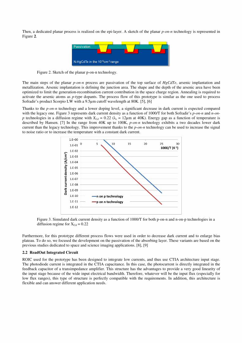
Then, a dedicated planar process is realized on the epi-layer. A sketch of the planar p-on-n technology is represented in
Figure 2.
Figure 2. Sketch of the planar p-on-n technology.
The main steps of the planar p-on-n process are passivation of the top surface of HgCdTe, arsenic implantation and
metallization. Arsenic implantation is defining the junction area. The shape and the depth of the arsenic area have been
optimized to limit the generation-recombination current contribution in the space charge region. Annealing is required to
activate the arsenic atoms as p-type dopants. The process flow of this prototype is similar as the one used to process
Sofradir’s product Scorpio LW with a 9.5µm cutoff wavelength at 80K. [5], [6]
Thanks to the p-on-n technology and a lower doping level, a significant decrease in dark current is expected compared
with the legacy one. Figure 3 represents dark current density as a function of 1000/T for both Sofradir’s p-on-n and n-on-
p technologies in a diffusion regime with XCd = 0.22 (λc = 12µm at 40K). Energy gap as a function of temperature is
described by Hansen. [7] In the range from 40K up to 100K, p-on-n technology exhibits a two decades lower dark
current than the legacy technology. This improvement thanks to the p-on-n technology can be used to increase the signal
to noise ratio or to increase the temperature with a constant dark current.
Figure 3. Simulated dark current density as a function of 1000/T for both p-on-n and n-on-p technologies in a
diffusion regime for XCd = 0.22
Furthermore, for this prototype different process flows were used in order to decrease dark current and to enlarge bias
plateau. To do so, we focused the development on the passivation of the absorbing layer. These variants are based on the
previous studies dedicated to space and science imaging applications. [8], [9]
2.2 ReadOut Integrated Circuit
ROIC used for the prototype has been designed to integrate low currents, and thus use CTIA architecture input stage.
The photodiode current is integrated in the CTIA capacitance. In this case, the photocurrent is directly integrated in the
feedback capacitor of a transimpedance amplifier. This structure has the advantages to provide a very good linearity of
the input stage because of the wide input electrical bandwidth. Therefore, whatever will be the input flux (especially for
low flux ranges), this type of structure is perfectly compatible with the requirements. In addition, this architecture is
flexible and can answer different application needs.

The specifications of the ROIC are described in Table 1. This ROIC presents two charge handling capacity, the first one
is 98 000 electrons to work in a high gain mode whereas the second one is 776 000 electrons to work in a low gain mode.
The read out noise are 20 electrons and 176, respectively. The power consumption of the ROIC is 150mW.
Table 1. ROIC specifications.
Parameters Specifications
Format 640*512
Pitch 15 µm
Input stage CTIA
Operating temperature range 40K – 300K
Correlated Double Sampling External Function
Power 150 mW
Frame frequency 60 Hz (maxi. with CDS)
120Hz without CDS
Video Output :
• Type
• Pixel Frequency
• Number of output
• Analogic
• 10 MHz
• 2 or 4
Integration Mode Rolling Shutter IWR
Integration Time User defined
High Gain
• Charge handling capa.
• Read out noise
• 98 000 e-
• 20e- @ 80K
Low Gain
• Charge handling capa.
• Read out noise
• 776 000 e-
• 170e-
Non linearity < ±1% @ 300K
2.3 Flip-chip hybridization
An important work has been done to optimize the CMOS ROIC preparation and hybridization. Hybridization is
performed by Indium bumps with a flip-chip equipment. This hybridization allows maintaining excellent process yield
and reliability at cryogenic operating temperature.
After flip-chip bonding, the initial CZT substrate is thinned down to the MCT absorbing layer. An antireflective coating
is deposited on the incoming light surface.
3. ELECTRICAL AND ELECTRO-OPTICAL PERFORMANCES
In this section all the characterizations performed on test chip and FPA are presented. Up to now, the low temperature
characterizations down to 40K are still running.

3.1 Test chip characterizations
After the detection circuit process, a first evaluation of the performances is done based on current measurements as a
function of voltage and as a function of temperature. These characterizations are performed on test chips. Two diodes per
variants and per wafer are characterized. The test chip is presented in Figure 4.
(a) (b)
Figure 4. (a) Test chip characterized after the technological process at a 15µm pitch, (b) SEM image of a single test chip.
The test chip presented in Figure 4 allows characterizing single diodes in a 15µm neighborhood. On Figure 4 (a),
different geometries/processes are included. Both neighboring diodes and the studied diode can be separately biased. For
all the characterizations presented in this section, both studied diode and neighboring ones are presenting the same bias.
Our set-up is presenting a significant photonic current for this cut-off wavelength. At 80K, the parasitic photonic current
density is in the range of 1 to 2.10-3
A/cm-2
.
Two designs of passivation have been studied for the development of this prototype. These designs are labeled A, B in
this paper. Design A corresponds to the standard design, the same as our product Scorpio LW. Design B is an improved
one.
First, the aim of design B is to enlarge the bias plateau in order to lower the contribution of band to band tunnel current.
In order to characterize it, i(V) characteristics are performed at 100K for the two designs and are presented in Figure 5,
squares and triangles are the experimental data.
Figure 5. Current as a function of reverse bias at 100K for the two designs A and B. Dots are experimental data, lines are the
simulated BTB current contributions at 100K and dotted lines are the extrapolated contribution of BTB current at 40K
As described in Figure 5, band to band tunnel (BTB) current is the limiting factor for large reverse bias; it has been
simulated using the geometrical parameters of the p on n junction at 100K for both designs. Thanks to design B,
dominant BTB tunnel current is minimized allowing the enlargement of the bias plateau by 0.5V compared to design A.

This modification in the process is successful. At 100K, focal plane arrays are not working at high reverse bias.
Nevertheless, as the operating temperature decreases, the HgCdTe energy band gap is decreasing too. As a consequence,
the BTB current becomes dominant at lower reverse bias. It is described by dotted lines in Figure 5 at 40K. The
simulations at 40K are extrapolated to the ones at 100K. Design B can be useful for low temperature and low flux
applications.
Second, design B is supposed to decrease dark current mean value by 30%. Thanks to i(V) characteristics, the mean
value of current is extracted at a reverse bias of -0.3V from 80K up to 140K. Then, a comparison between designs A and
B is operated leading to Table 2.
Table 2. Decrease of current mean value thanks to design B compared to design A.
T(K) 1000/T (K-1
) Decrease of current Comments
80 12.5 -1% Photonic current
100 10 -23%
Diffusion current 120 8.3 -37%
140 7.1 -22%
According to the results presented in Table 2, photonic current is comparable for the two designs. On the other hand,
dark current, in the diffusion regime is decreased between 20 and 37% thanks to design B compared to design A.
3.2 FPA characterization at 80K
In this section, all the characterizations are performed at 80K. A 3.1° field of view was used under illumination. This
aperture was chosen to lower the photonic current allowing a proper measurement with low integration time. The
integration time was set to 324µs for half well fill. At this temperature for such long wavelength infrared detectors, a
significant contribution of the collected current corresponds to dark current. In front of a 25°C black body, about 20% of
the DC level collected by the ROIC corresponds to dark current.
Responsivity measurements have been performed using two blackbody temperatures, 20-30°C. Figure 6 represents the
responsivity histogram at 79K under illumination.
Figure 6. Responsivity histogram under illumination, 79K and 20-30°C BB.
This first prototype presents a homogeneous responsivity with a Gaussian distribution of the pixels. Mean value of the
responsivity 3.07pA/K. Such homogeneity in response illustrates the high level of quality of the epilayer in terms of
crystallinity, control of its thickness and Cadmium content. Some white pixels are appearing on the mapping. These
pixels are corresponding to defective ones. These isolated pixels are attributed to saturated pixel or pixels mainly

dominated by dark current. The defective pixels are attributed to the technological process. These defects should be
significantly decreased thanks to an increase in the maturity of the technology.
The RMS noise has been characterized. It can be compared to the current shot noise (theoretical ideal noise). The ratio
between the two is around 1. This value indicates that the photodiodes do not present any excess noise and thus are
limited by current shot noise.
Then, NETD (Noise Equivalent Temperature Difference) has been characterized with a 25°C BB. NETD histogram is
presented in Figure 7.
Figure 7. NETD histogram under illumination, 79K and 25°C BB.
The mean value of NETD is 110mK. This value is in agreement with the measurement conditions (high F number, dark
current noise contribution, and operating temperature 79K). Despite the dots with higher NETD, corresponding to a
small tail on the histogram (Figure 7), the performances of this first prototype are promising.
Table 3 is summarizing the performances of this first prototype using design A. Cutoff wavelength has been evaluated
for this FPA to 11.12µm at 78K which corresponds to 12.4µm at 40K.
Table 3. Main performances of the first prototype, at 79K
Mean
value
IR flux current (pA) 212.10
Dark current (pA) 39.59
Photonic current (pA) 172.40
Responsivity (pA/K) 3.07
IR flux RMS noise (mV) 1.40
IR flux excess noise 0.99
NEDT (mK) 109.50
Dark RMS noise (mV) 1.40
Dark excess noise 1.01

In order to compare the two designs, the performances of two FPAs are compared, one with the improved design and the
one presented above. It is summarized in Table 4.
First, the responsivity is nearly the same between the two FPA. It is 4% lower for the design B FPA. This value is
interpreted by a shorter cutoff wavelength of design B FPA equal to 11.06µm at 78K. Dark current is significantly
reduced for design B FPA compared with design A one. It is divided by a factor of 2.2 from variant A to variant B. Dark
current reduction is not fully attributed to the improvement of the technology. Part of the reduction of dark current comes
from the shorter cutoff wavelength of the design B FPA. Nevertheless, 35% of the reduction of dark current is attributed
with design B is attributed to the improvement of the technology.
Table 4. Comparison of the performances for the two designs A and B at 79K.
Variant Design A Design B
Under
flux
conditions
Current (pA) 212.1 184.6
Resp. (pA/K) 3.07 2.96
NETD (mK) 109.5 104.1
Under dark
conditions
Current (pA) 39.6 17.4
Excess noise 1.01 1.00
Despite the difference of cutoff wavelength, NETD of design B FPA remains lower than design A FPA. A complete
characterization of these two FPAs has to be performed at lower temperature soon.
3.3 First evaluation at low temperature
An improved FPA has been characterized at low temperature down to 60K with a helium gas cryostat. Current-voltage
measurements have been done (Figure 8): under dark conditions, the bias plateau is over 550mV at 80K and is more than
250mV at 60K. This last value is a mean one with a filter to exclude high defective pixels. At higher bias, leakage
current attributed to BTB tunneling current becomes dominant.
Figure 8. Current-voltage characteristics for an improved FPA for different operating temperatures.

Figure 9 presents the evolution of dark current density with operating temperature down to 60K. The dark current density
is below the Rule07 from 80K down to 60K. But it decreases with a pure diffusion-type law (exp����
�) from 80K down
to 60K and so, slower than the one of Rule07. [10] This result is very promising but has yet to be confirmed at lower
temperature in order to determine at which temperature the transition to another limiting regime occurs and if it would be
enough to meet the requirements of this study.
Figure 9. Arrhenius plot of dark current density, dots are data, dashed line is simulation of the diffusion dark
current and dotted in the Rule 07.
4. CONCLUSION
Sofradir and the CEA-LETI have realized a prototype based on the HgCdTe p-on-n technology with a 12µm cutoff
wavelength at 40K. ROIC used for this prototype is based on a CTIA input stage with two different gains.
Characterizations have been performed and presented in this paper down to 60K. Two designs of detection circuit have
been studied; the first one is close to Scorpio LW product whereas the second one is improved for low flux and low
temperature applications. Thanks to the second design, on one hand a decrease in dark current has been demonstrated
and evaluated to -35%, and on the other hand an increase in the bias plateau is achieved thanks to lowering the tunnel
current contribution.
5. ACKNOWLEDGMENT
The authors would like to thank all the SOFRADIR and CEA-Leti (LIR) teams, dedicated to quality work. The authors
would like to thank the European Space Agency (ESA) for funding this study through ESA Contract
4000113066/15/NL/RA.
REFERENCES
[1] Bouakka-Manesse A., Jamin N., Delannoy A., Fieque B., Leroy C., Pidancier P., Vial L., Chorier P. and Péré-
Laperne N., "Space activity and programs at SOFRADIR," Proc. SPIE 9981, 998109 (2016).
[2] Destéfanis G., "Electrical doping of HgCdTe by ion implantation and heat treatment," J. Crystal Growth 86, 700
(1988).
[3] Castelein P., Baier N., Gravrand O., Mollard L., Brellier D., Rochette F., Kerlain A., Rubaldo L., Reibel Y. and
Destefanis G., "Latest developments on p-on-n HgCdTe architectures at DEFIR," Proc. SPIE 9070, 90702Y-1
(2014).
[4] Brellier D., Gout E., Gaude G., Pelenc D., Ballet P., Miguet T. and Manzato M. C., "Bulk Growth of CdZnTe:
Quality Improvement and Size Increase," Journal of Electronic Materials, 0361-5235 (2014).

[5] Péré-Laperne N., Taalat R., Berthoz J., Rubaldo L., Carrère E., Dargent L. and Kerlain A., "Improvements of
long wave p on n HgCdTe infrared technology ", Proc. SPIE 9933, 99330H (2016).
[6] Rubaldo L., Taalat R., Berthoz J., Maillard M., Péré-Laperne N., Brunner A., Guinedor P., Dargent L.,
Manissadjian A., Reibel Y. and Kerlain A., "Latest improvements on long wave p on n HgCdTe Technology at
Sofradir," Proc. SPIE 10177, 101771E-1 (2017).
[7] Hansen, G. L., "Energy gap versus alloy composition and temperature in Hg1-xCdxTe," Journal of Applied
Physics 53(10), 7099-7101 (1982).
[8] Baier N., Mollard L., Gravrand O., Bourgeois G., Zanatta J. P., Destefanis G., Pidancier P., Chorier P.,
Tauziède L. and Bardoux A., "Very long wavelength infrared detection with p-on-n LPE HgCdTe," Proc. SPIE
8353, 83532N (2012).
[9] Gravrand O., Rothman J., Castelein P., Cervera C., Baier N., Lobre C., De Borniol E., Zanatta J. P., Boulade O.,
Moreau V., Fieque B. and Chorier P., "Latest achievements on MCT IR detectors for space and science
imaging," Proc. SPIE 9819, 98191W-1 (2016)
[10] Tennant, W.E., "Rule 07 Revisited: Still a good heuristic predictor for p/n HgCdTe Photodiode performance," J.
of Electronic Materials, Volume 39, Issue 7, pp. 1030-1035 (2010).

Ed
ition
: 11-
17373 US Hwy 46W Fairfield, NJ 07004 973-882-0211 Fax: 973-882-0997 [email protected] www.sofradir-ec.com
For more information on our Products visit:
www.sofradir-ec.com