low electrical resistivity in thin and ultrathin copper ... electrical resistivity in thin and...
TRANSCRIPT

Low electrical resistivity in thin and ultrathin copper layers grown by high powerimpulse magnetron sputteringFelipe Cemin, Daniel Lundin, Davide Cammilleri, Thomas Maroutian, Philippe Lecoeur, and Tiberiu Minea Citation: Journal of Vacuum Science & Technology A 34, 051506 (2016); doi: 10.1116/1.4959555 View online: http://dx.doi.org/10.1116/1.4959555 View Table of Contents: http://scitation.aip.org/content/avs/journal/jvsta/34/5?ver=pdfcov Published by the AVS: Science & Technology of Materials, Interfaces, and Processing Articles you may be interested in On the pressure effect in energetic deposition of Cu thin films by modulated pulsed power magnetron sputtering:A global plasma model and experiments J. Appl. Phys. 117, 203302 (2015); 10.1063/1.4921443 Giant magnetization on Mn3Ga ultra-thin films grown by magnetron sputtering on SiO2/Si(001) J. Appl. Phys. 117, 123902 (2015); 10.1063/1.4916158 Probing thickness-dependent dislocation storage in freestanding Cu films using residual electrical resistivity Appl. Phys. Lett. 93, 041901 (2008); 10.1063/1.2961006 Electrical resistivity of Cu films deposited by ion beam deposition: Effects of grain size, impurities, andmorphological defect J. Appl. Phys. 99, 094909 (2006); 10.1063/1.2194247 Real time resistivity measurements during sputter deposition of ultrathin copper films J. Appl. Phys. 91, 1667 (2002); 10.1063/1.1430530
Redistribution subject to AVS license or copyright; see http://scitation.aip.org/termsconditions. IP: 90.225.37.173 On: Mon, 08 Aug 2016 08:46:48

Low electrical resistivity in thin and ultrathin copper layers grown by highpower impulse magnetron sputtering
Felipe Cemina) and Daniel LundinLaboratoire de Physique des Gaz et des Plasmas (LPGP), Unit�e Mixte de Recherche 8578 CNRS,Universit�e Paris-Sud, 91405 Orsay, France
Davide CammilleriLaboratoire de Physique des Gaz et des Plasmas (LPGP), Unit�e Mixte de Recherche 8578 CNRS,Universit�e Paris-Sud, 91405 Orsay, France and Institut d’ �Electronique Fondamentale (IEF), Unit�e Mixte deRecherche 8622 CNRS, Universit�e Paris-Sud, 91405 Orsay, France
Thomas Maroutian and Philippe LecoeurInstitut d’ �Electronique Fondamentale (IEF), Unit�e Mixte de Recherche 8622 CNRS, Universit�e Paris-Sud,91405 Orsay, France
Tiberiu MineaLaboratoire de Physique des Gaz et des Plasmas (LPGP), Unit�e Mixte de Recherche 8578 CNRS, Universit�eParis-Sud, 91405 Orsay, France
(Received 3 May 2016; accepted 12 July 2016; published 25 July 2016)
Ultrathin copper (Cu) layers are in continuous demand in several areas, such as within
microelectronics and space, as well as in instrumentation technology requiring an electrical
resistivity as low as possible. However, the performance of modern copper connections is limited
by the size-dependent value of the film resistivity, which is known to increase when the layer thick-
ness is reduced to a few tens of nanometer. In this work, the authors have successfully deposited
Cu thin films from 20 to 800 nm exhibiting reduced electrical resistivity by using a high power
impulse magnetron sputtering (HiPIMS) process. The electrical and microstructural properties of
such films were compared to samples deposited by conventional direct current magnetron sputter-
ing (DCMS) within the same thickness range. For films as thin as 30 nm, the electrical resistivity
was reduced by �30% when deposited by HiPIMS compared to DCMS, being only three times
larger than the copper bulk value. The HiPIMS Cu films exhibit larger grain size and reduced grain
boundary density, which reduce the scattering of charge carriers and thereby the resistivity of the
thin film. These larger grains are likely due to the highly ionized precursor flux of the HiPIMS dis-
charge, which in the present work is controlled by an external substrate bias. VC 2016 AmericanVacuum Society. [http://dx.doi.org/10.1116/1.4959555]
I. INTRODUCTION
As a bulk material, copper is one of the most employed
metals in the manufacturing industries for a variety of appli-
cations due to its high electrical and thermal conductivities.
In the last decades, this metal has also attracted much inter-
est as a thin and ultrathin film material, which was driven by
the increasing demand for nanoranged downscaled electrical,
electronic, and magnetic devices.1 For instance, copper is
replacing aluminum and its alloys as an interconnect mate-
rial in submicron ultralarge scale integrated circuits, since it
presents lower bulk electrical resistivity (qCu¼ 1.67 vs
qAl¼ 2.65 lX cm), better electromigration resistance, higher
melting temperature (TCu¼ 1360 vs TAl¼ 930 K), and higher
resistance under stress failures.1–5 Copper thin films have
also been studied to be used as a spacer layer between two
ferromagnetic layers in spin valve structures based on the
giant magnetoresistance (GMR) effect, for magnetic field
sensors and read-out heads in high density magnetic record-
ing, microelectromechanical systems, and magnetic random-
access memory.6–8 Continuous efforts are being made in
terms of increasing the performance of such devices, which
is strongly dependent on the microstructure, electrical prop-
erties, and growth process of copper films.
The interest of having ultrathin copper layers with electri-
cal resistivity as close as possible to the bulk value is central
for the proper functioning of microdevices, since high resis-
tivity results in larger heat dissipation and interconnect
delay, which limits operation in high frequency circuits.9
However, as the required dimensions reach the nanoscale,
the increase in electrical resistivity of a metal thin film is
expected.10 This size-dependent regime is reached when the
thickness of the film becomes comparable to the electron
mean free path for electron–phonon collisions (39 nm for
copper), resulting in a dramatic increase of the resistivity
above that of the bulk material, even at room tempera-
ture.9,11,12 It is associated with free-electron scattering at
external surfaces and higher grain density resulting in inter-
nal free-electron scattering at grain boundaries, as well as
other minor factors as inhomogeneous film growth,
decreased island growth, surface roughness, impurities, and
poor film crystallinity.4,12–16 Indeed, previous works have
shown that the resistivity of copper thin films increases from
bulk value to several lX cm when the layers are in thea)Electronic mail: [email protected]
051506-1 J. Vac. Sci. Technol. A 34(5), Sep/Oct 2016 0734-2101/2016/34(5)/051506/7/$30.00 VC 2016 American Vacuum Society 051506-1
Redistribution subject to AVS license or copyright; see http://scitation.aip.org/termsconditions. IP: 90.225.37.173 On: Mon, 08 Aug 2016 08:46:48
nanoscale range.3,5,10,17–19 Therefore, the understanding and
control of this size-dependent phenomenon is a major con-
cern and a key issue to the entire microelectronics industry,
since copper is expected to continue dominating the inter-
connect technology.9,11
Most copper thin films are grown by physical vapor depo-
sition (PVD) processes, in particular, by conventional direct
current magnetron sputtering (DCMS),2–4,17,20–22 and by
metal-organic chemical vapor deposition (MOCVD).15,23–25
Compared to the conventional PVD processes, the copper
films deposited by CVD exhibit a better step coverage and
higher deposition rates. However, MOCVD requires a com-
plicated processing system with the use of metal organic
compounds, higher deposition temperatures (�180–400 �C),
and the need of a postannealing process to improve the thin
film smoothness, crystallinity, and electromigration.15,23 A
promising alternative deposition method is a PVD process
called high power impulse magnetron sputtering
(HiPIMS),26,27 which generates a high ionization fraction of
the sputtered vapor (typically >50%) during the pulse.27 The
high ionization fraction results in better control of the film
growth, even at room temperature, as it allows for control of
the energy and direction of the film-forming species, which
affects the phase composition, microstructure, and final
properties of the resulting film.26,28 This is a significant
advantage over DCMS, where the sputtered vapor consists
mainly of neutral species.29 However, no reports were found
concerning the electrical and microstructural properties of
ultrathin copper films grown by HiPIMS. It should be men-
tioned that Cu films have been deposited by HiPIMS for
other purposes.30–32
Therefore, in the present work, we have grown copper
thin and ultrathin films by DCMS and HiPIMS and systemat-
ically studied and compared their electrical and microstruc-
tural properties as a function of thickness and deposition
process, with the ultimate goal of reducing the resistivity of
copper layers in the size-effect regime (�100 nm).
II. EXPERIMENT
The studied copper thin films were deposited onto p-type
doped Si (100) substrates (qSi¼ 8–16 X cm) using both
DCMS and HiPIMS configurations. All experiments were
carried out in a custom build vacuum chamber evacuated by
a turbomolecular pump to a base pressure below 3 �10�4 Pa. The deposition system is equipped with a Lesker
Torus 2 in. top-mounted water-cooled magnetron, which is
operated by a HiPIMS power supply (HiPSTER 1, Ionautics,
Sweden) or a DC power supply (SR1.5-N-1500, Technix,
France). The deposition system also includes a load-lock
chamber for transferring samples and a movable sample hol-
der facing the target, which is connected to a negative DC
bias power supply (SR1-N-300, Technix, France). The target
to substrate distance was fixed at 9 cm for all experiments.
Prior to film deposition, each Si substrate was cleaned
ultrasonically in acetone (30 min) and isopropanol (30 min)
and then loaded into the deposition chamber. All the samples
were Ar ion etched for 5 min at a total pressure of 1.5 Pa
using a 13.56 MHz radio-frequency (RF) power supply with
an incident power of 100 W (without magnetron operation).
The RF plasma was generated in a metal coil placed in situjust above the samples, and the Ar ions were accelerated
toward to the substrates by applying a DC bias voltage of
�300 V to the sample holder.
Subsequently, the copper films were grown using Ar
(99.997% purity) as a neutral gas to bombard a copper target
of 50.8 mm in diameter and 3 mm thickness (99.99% purity)
at a total pressure of 0.5 Pa. An average power of 100 W was
kept constant in all experiments for both DCMS and
HIPIMS configurations. For the DCMS experiments, the tar-
get voltage during the discharge was 400 V, and the target
current was 250 mA. For the HiPIMS experiments, square
voltage pulses of �650 V with 40 ls pulse-on time and a
pulse frequency of 500 Hz (duty cycle of 2%) were applied
to the cathode. The average peak current value was 20 A
(peak target current density of 1 A cm�1). The recorded dis-
charge pulse characteristics for typical HiPIMS conditions
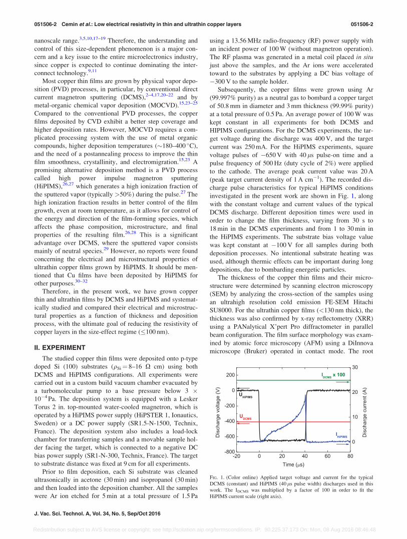
investigated in the present work are shown in Fig. 1, along
with the constant voltage and current values of the typical
DCMS discharge. Different deposition times were used in
order to change the film thickness, varying from 30 s to
18 min in the DCMS experiments and from 1 to 30 min in
the HiPIMS experiments. The substrate bias voltage value
was kept constant at �100 V for all samples during both
deposition processes. No intentional substrate heating was
used, although thermic effects can be important during long
depositions, due to bombarding energetic particles.
The thickness of the copper thin films and their micro-
structure were determined by scanning electron microscopy
(SEM) by analyzing the cross-section of the samples using
an ultrahigh resolution cold emission FE-SEM Hitachi
SU8000. For the ultrathin copper films (<130 nm thick), the
thickness was also confirmed by x-ray reflectometry (XRR)
using a PANalytical X’pert Pro diffractometer in parallel
beam configuration. The film surface morphology was exam-
ined by atomic force microscopy (AFM) using a DiInnova
microscope (Bruker) operated in contact mode. The root
FIG. 1. (Color online) Applied target voltage and current for the typical
DCMS (constant) and HiPIMS (40 ls pulse width) discharges used in this
work. The IDCMS was multiplied by a factor of 100 in order to fit the
HiPIMS current scale (right axis).
051506-2 Cemin et al.: Low electrical resistivity in thin and ultrathin copper layers 051506-2
J. Vac. Sci. Technol. A, Vol. 34, No. 5, Sep/Oct 2016
Redistribution subject to AVS license or copyright; see http://scitation.aip.org/termsconditions. IP: 90.225.37.173 On: Mon, 08 Aug 2016 08:46:48

mean square (RMS) roughness and the average grain size
were estimated over AFM images with an area of 2 � 2 lm2
with the image analysis tools of the WSXM software.33 The
thin films’ electrical resistivity was measured at room tem-
perature by the four-point probe method, with a Keithley
precision current source and a Keithley nanovoltmeter, on
two different setups: first with a Jandel multiheight cylindri-
cal probe and second by placing four probes at the corner of
the sample in the so-called van der Pauw configuration.
Equation (1) was used to obtain the electrical resistivity q of
the copper thin films in both methods, which is related to the
thickness h of the copper layer, the current I passed through
the outer probe tips, and the voltage V measured between the
inner probe tips. The resistivity values found by the van der
Pauw method were in good agreement with the values mea-
sured by the four-point probe method. Thus, the final resis-
tivity values reported in this work are average values
obtained for each sample using both methods and based on
approximately six measurements
q ¼ pln2
V
Ih: (1)
We also investigated the low temperature effect on the
resistivity of ultrathin (�60 nm thick) copper films grown by
DCMS and HiPIMS, using a Linkam temperature controlled
stage. The temperature was decreased at 10 K min�1 using
liquid nitrogen from 293 K (room temperature) to 120 K.
The process was interrupted every 2 min in order to collect
the electrical data using the van der Pauw method.
III. RESULTS AND DISCUSSION
A. Overview
Typical cross-sectional SEM images of two Cu samples
are shown in Figs. 2(a) and 2(b), illustrating the microstruc-
ture of copper thin films grown by DCMS (5 min) and
HiPIMS (11 min), respectively. Both images exhibit a com-
pact �300 nm thick layer deposited on top of the silicon sub-
strate. However, the structural evolution during film growth
seems to differ for the different deposition processes for the
same film thickness. The DCMS film exhibits a fibrous
columnar structure [Fig. 2(a)] with small grains protruding
from the top surface, while the microstructure of the
HiPIMS films appears denser (globular grains), with a
smoother top surface [Fig. 2(b)]. The respective microstruc-
tures shown in Fig. 2 are typical for all the DCMS and
HiPIMS Cu films studied in this work, although the Cu
thickness of the deposited samples varied in the submicro-
metric range. Such differences with generally smoother and
denser thin films when using HiPIMS as compared to DCMS
have previously been reported by Samuelsson et al.34 when
investigating eight different metal coatings, including Cu.
Figure 3 shows the film thickness as a function of deposi-
tion time for the samples deposited by DCMS and HiPIMS.
As expected, the film thickness increases with deposition
time for both techniques, due to accumulation of deposited
material over time. The linear behavior is characteristic of
time-dependent growth of metallic films by sputtering-
deposition technologies and allows us to obtain a reliable
and reproducible growth rate of the deposited films. In this
work, the deposition rate of Cu films was found to be
28 6 0.5 nm min�1 for HiPIMS and 61 6 1.5 nm min�1 for
DCMS, i.e., the relative HiPIMS/DCMS deposition rate was
approximately 47%. Similar relative deposition rates of Cu
have earlier been reported in the literature, with values lying
between 40% and 60%, depending on the different experi-
mental setups.34,35 There are several reasons for the
FIG. 2. Cross-sectional SEM images of the samples with the Cu thin film
deposited by DCMS for 5 min (a) and by HiPIMS for 11 min (b). The thick-
ness of the deposited layer is around 300 nm for both samples.
FIG. 3. (Color online) Thickness of the Cu films deposited by DCMS and
HiPIMS as a function of deposition time.
051506-3 Cemin et al.: Low electrical resistivity in thin and ultrathin copper layers 051506-3
JVST A - Vacuum, Surfaces, and Films
Redistribution subject to AVS license or copyright; see http://scitation.aip.org/termsconditions. IP: 90.225.37.173 On: Mon, 08 Aug 2016 08:46:48

reduction in deposition rate in HiPIMS, but the main mecha-
nism is likely back-attraction of metal ions to the target due
to an extended plasma presheath followed by self-sputtering,
which causes a reduction in the amount of sputtered particles
reaching the substrate.36 Other effects are discussed in detail
elsewhere.26
B. Microstructural properties
Figure 4 shows 2 � 2 lm2 AFM top view micrographs of
selected Cu films with different thicknesses deposited by
DCMS [Figs. 4(a)–4(c)] and HiPIMS [Figs. 4(d)–4(f)]. One
can see that all surfaces exhibit a granular structure, with
increased in-plane grain size at higher thicknesses for both
DCMS and HiPIMS Cu films. The observed grain size
increase with thickness was previously reported for thin cop-
per layers deposited by DCMS (Ref. 3) and filtered cathodic
vacuum arc (FCVA)5 and is typical for deposition of high
mobility metals.37 It is attributed to surface energy minimi-
zation during film growth at longer times, which means that
fine grains evolve during the coalescence and coarsening
processes and continues to evolve by grain boundary motion
as the film thickness increases, which reduces the total grain
boundary area (and energy).37 However, it is important to
note that the HiPIMS Cu films are composed of larger grains
compared to the corresponding DCMS films at the same
average thickness, confirming what was also observed in the
SEM images (Fig. 2). Table I presents the estimated average
grain size of each sample shown in Fig. 4. Taking all meas-
urements into account, the HiPIMS/DCMS grain size frac-
tion varies between 1.7 and 2.1, which means that, roughly,
the grains formed in the HiPIMS films are twice the size of
the grains of the DCMS films. More detailed grain size
investigations using XRD analysis are being carried out and
will be addressed in a future paper, which will investigate
the fundamentals of Cu films during the early stages of
growth (which is out of scope of the present paper).
In all cases, the RMS roughness increases with the thick-
ness of the studied Cu films, as shown in Table I. It is associ-
ated with the increase in grain size at higher deposition
times, i.e., at larger film thickness, as observed in the AFM
images (Fig. 4) and discussed elsewhere.5 One can notice
small differences in the RMS roughness values of DCMS
and HiPIMS films with the same average thickness (direct
comparison of columns 3 and 6, Table I). The �120 nm thick
films appear to be rougher when deposited by HiPIMS than
by DCMS, which may be associated with the large grains
present in the films deposited by the pulsed technique. On
the other hand, for thicker coatings, HiPIMS films have
somewhat smaller roughness, which has often been reported
in the literature.28,38
The large grained, dense, columnar morphology found in
the HiPIMS Cu films is related to the increased adatom
mobility and enhanced diffusion processes, which are typical
in this type of discharge, due to the high amount of ions in
the flux of the sputtered material.26 Moreover, the pulsed
character of the deposition process also changes the growth
kinetics39 and favors surface reorganization between pulses.
It results in increased self-diffusion of surface and grain
boundaries promoting grain coarsening during growth,
which ultimately leads to larger grain size. Furthermore,
from transmission electron microscopy studies by Petrov
et al.,40 it is known that an increase in the ion flux greatly
reduces intracolumnar as well as intercolumnar porosity,
where it is suggested that the incoming ions collisionally
enhance the surface mobility. Kouznetsov et al.30 estimated
the ionized flux fraction for HiPIMS sputtering of Cu in an
Ar atmosphere to approximately 70% and Vlcek et al.41
measured the Cuþ fraction of the total ion flux to the sub-
strate to almost 92%, which is far beyond estimated DCMS
values of a few per cent or less.42
FIG. 4. (Color online) AFM images of the top surface of Cu thin films with different thicknesses grown by DCMS (a)–(c) and HiPIMS (d)–(f).
051506-4 Cemin et al.: Low electrical resistivity in thin and ultrathin copper layers 051506-4
J. Vac. Sci. Technol. A, Vol. 34, No. 5, Sep/Oct 2016
Redistribution subject to AVS license or copyright; see http://scitation.aip.org/termsconditions. IP: 90.225.37.173 On: Mon, 08 Aug 2016 08:46:48

Combining the results in Figs. 2 and 4, it is concluded
that for the DCMS case, where the sputtered vapor is mainly
constituted by neutrals with a kinetic energy of a few elec-
tron volt, the microstructure is characterized by a fine-
grained structure of textured and fibrous grains, pointing in
the direction of the arriving vapor flux and ending with
domed tops. Such a microstructure with a high grain density
is typical for zone 1 type of thin films according to the origi-
nal structure zone diagram by Movchan and Demchishin.43
The HiPIMS films are on the other hand characterized by
larger grains due to the increase in energy provided by the
ion assistance, which also leads to film densification and pos-
sibly renucleation. These features are associated with zone 3
in the revised version of the structure zone diagram, where
ion bombardment is included.44 The top surface is also fac-
eted due to the larger grains.
C. Electrical resistivity
The dependence of the electrical resistivity at room tem-
perature on the thicknesses of Cu films deposited by DCMS
and HiPIMS is illustrated in Fig. 5 (closed red squares and
blue circles, respectively). For both deposition processes,
one can notice an exponential decay of electrical resistivity
as the Cu film thickness is increased, which eventually con-
verges close to the bulk value of polycrystalline copper for
the thicker films (400 nm thick or more). The thinnest
DCMS and HiPIMS Cu films (�30 nm) prepared in this
work exhibited the highest resistivity values, 8.2 and 5.8 lX
cm, respectively. The observed trends are in agreement with
previously reported theories and experiments concerning the
size-related scaling of the resistivity of conducting metallic
thin films. If we look at the Cu films deposited by DCMS,
Chan et al.3 found an electrical resistivity equal to 14.81 lXcm for the thinnest layer (130 nm thick) studied in their work
(open green squares, Fig. 5) and Cabral et al.17 reported a
resistivity equal to 9.5 lX cm for a 100 nm thick sputtered
Cu film alloyed with chromium 1 at. % (open pink circles,
Fig. 5). In both studies, the resistivity decreases with increas-
ing film thickness and eventually approaches the bulk value.
Nonetheless, Shi et al.5 obtained Cu films with lower resis-
tivity by using a FCVA technique, with the highest value of
3.6 lX cm for the 25 nm thick film and an average value of
1.8 lX cm for the films with a thickness >135 nm (open
orange triangles, Fig. 5).
The most striking result of the present study is that the
electrical resistivity of all HiPIMS films is smaller than the
corresponding resistivity values found for the DCMS films
(Fig. 5). The percentage decrease in electrical resistivity is
around 30% for the films grown by HiPIMS compared to the
DCMS ones, if we consider the films <200 nm thick. It is
important to note that the observed decrease in resistivity
occurs even for the ultrathin films, which are the most suit-
able candidates for downscaling microelectronic devices. In
addition, the thicker HiPIMS films tend to stabilize their
resistivity at �2.3 lX cm, while the same occurs for the
DCMS films at �3 lX cm (25% of reduction). Previous
reports have also confirmed the variation of resistivity in
thin films grown by DCMS and HiPIMS: Samuelsson
et al.28 have shown that chromium thin films grown by
HiPIMS have lower electrical resistivity than their counter-
part deposited by DCMS (�32% of reduction), and the same
trend was observed by Magnus et al.14 for titanium nitride
thin films (�85% of reduction). Finally, one can observe in
Fig. 5 that HiPIMS films with thicknesses between 250 and
350 nm exhibit an unexpected resistivity increase. Several
samples deposited in different batches were investigated to
verify this trend. We currently do not have an explanation
for the sudden change in resistivity. Nevertheless, the
HiPIMS values are still below the DCMS values even in this
thickness region (�10% reduction).
The overall differences in the electrical resistivity
obtained by DCMS and HiPIMS (Fig. 5) are believed to be
related to the previously discussed microstructural differ-
ences of the Cu films (Figs. 2 and 4), which are associated
with different grain evolution during film growth in both
deposition processes. For the DCMS samples, the small
TABLE I. Average grain size and RMS roughness obtained from the AFM images shown in Fig. 4 for the investigated DCMS and HiPIMS Cu films.
DCMS HiPIMS
Thickness (nm) Average grain size (nm) RMS roughness (nm) Thickness (nm) Average grain size (nm) RMS roughness (nm)
125 23 1.12 115 40 1.90
290 55 6.80 200 100 5.92
600 85 6.50 520 150 6.35
FIG. 5. (Color online) Electrical resistivity at room temperature of the Cu thin
films studied in this work, grown by DCMS (closed red squares) and HiPIMS
(closed blue circles), and of the Cu films grown by Chan et al. (Ref. 3) (open
green squares), Cabral et al. (Ref. 17) (open pink circles) and Shi et al. (Ref. 5)
(open orange triangles), as a function of their thicknesses. The resistivity bulk
value of polycrystalline Cu is also presented (1.67 lX cm).
051506-5 Cemin et al.: Low electrical resistivity in thin and ultrathin copper layers 051506-5
JVST A - Vacuum, Surfaces, and Films
Redistribution subject to AVS license or copyright; see http://scitation.aip.org/termsconditions. IP: 90.225.37.173 On: Mon, 08 Aug 2016 08:46:48

grain size and the large number of grain boundaries are
likely responsible for the higher resistivity, because grain
boundaries act as scattering centers for free-electrons.9,11
The HiPIMS films exhibit larger grains, which reduce the
grain boundary density and scattering of charge carriers, and
thereby improving their mobility and consequently reducing
the resistivity of the thin film.12,13 The suggestion of grain
size governing the free-electron transport in metallic thin
films seems to be even more relevant if we look at the almost
equal average grain size of the 290 nm thick film obtained by
DCMS and the 115 nm thick film obtained by HiPIMS
(Table I). The resistivity values for these two samples are
the same, as can be seen in Fig. 5, horizontal black bold line
(�3.4 lX cm). Although not a direct proof, this is an indica-
tion of the correlation between the microstructure and the
electrical resistivity. In addition, Harper et al.13 claimed that
there is an inverse linear dependence of film resistivity on
grain size, which was also verified as a trend for selected
samples studied in this work (not shown). The same behavior
was demonstrated for Cu films deposited by MOCVD.45
Finally, Chawla et al.12 have shown that it is possible to
reduce the resistivity by 10%–15% of 30–50 nm thick poly-
crystalline Cu layers by increasing the average grain size by
a factor of 1.8. In the present study, for approximately the
same factor, we found a 10%–30% improvement in the resis-
tivity of 30–800 nm Cu films, by modifying the deposition
process (HiPIMS vs DCMS).
The results shown in Fig. 5 also allow us to evaluate the
electrical resistivity of Cu films depending on the type of
PVD process used. One can see that the resistivity of the
HiPIMS films is lower than the resistivity of all DCMS films,
but higher compared to the FCVA films. As previously dis-
cussed, the ionization degree of the cathode material in the
HiPIMS discharges is higher than in DCMS discharges, lead-
ing to films with larger grains and reduced resistivity. The
even better results found for the FCVA Cu films5 are, in the
same way, likely due to the almost fully ionized precursor
flux of the FCVA method,46 which enables acceleration of all
impinging particles to the substrate by the use of a substrate
bias and ultimately a favorable microstructure, in line with the
discussion on ionized film growth in Sec. III B. Even though
the HiPIMS values of the Cu thin films resistivity are slightly
higher than the ones found for the FCVA films, the worldwide
availability of magnetron systems makes the HiPIMS solution
more attractive, since it uses conventional magnetron sputter-
ing equipment except for the power supplies.
The electrical resistivity of one set of these ultrathin
HiPIMS/DCMS Cu films (�60 nm) was also studied with
respect to the operating temperature, due to the interest of
investigating the metallicity of the Cu films as well as oper-
ating devices such as magnetic field sensors well below
room temperature. The results are shown in Fig. 6. As
expected, the resistivity of both copper layers decreases line-
arly as the temperature decreases. The HiPIMS Cu film has a
lower resistivity compared to the DCMS film (30% decrease)
at all evaluated temperatures. Note that the slope of the
HiPIMS sample is slightly steeper (0.00652 lX cm K�1
compared to 0.00524 lX cm K�1 for the DCMS sample),
which indicates a higher metallicity and a better crystal qual-
ity of the HiPIMS Cu film. This is especially interesting for
applications sensitive to electron scattering from defects
such as GMR devices.
IV. SUMMARY AND CONCLUSIONS
We have studied the electrical and microstructural proper-
ties of Cu thin and ultrathin films grown by DCMS and
HiPIMS. A strong correlation between the electrical resistiv-
ity and the grain size was found, where the HiPIMS films
exhibit larger grain size (approximately by a factor of 2) and
lower electrical resistivity (approximately 30% reduction)
compared to the DCMS films of similar thickness. These
results were explained in light of the high energetic species
produced in the HiPIMS discharges and impinging on the
substrate, which affect the adatom mobility and surface and
grain boundary self-diffusion during film growth. It leads to
a reduction of the total grain boundary area of the deposited
samples, and a decreased scattering of free-electrons, result-
ing in a lower resistivity. An improved conductivity and
metallicity of ultrathin HiPIMS films was found also for low
temperature operation. The strategy used in the present study
to deposit ultrathin Cu films by HiPIMS could be useful for
the microelectroelectronic-magnetic industries, which
require a reduction of the thickness-dependent resistivity of
Cu films in their devices.
ACKNOWLEDGMENTS
This work was supported by the French National Center
for Scientific Research (CNRS), the Brazilian National
Council of Scientific and Technological Development
(CNPq—“Ciencia sem Fronteiras”) through Project No.
233194/2014-2 and the LabeX LaSIPS (ANR-10-LABX-
0040-LaSIPS)—Project BOLTO—managed by the French
National Research Agency under the “Investissementsd’avenir” program (No. ANR-11-IDEX-0003-02). F.C. is
supported by CNPq. The authors are grateful to Universit�eParis-Sud, LPGP, and CTU IEF-Minerve, which is partly
FIG. 6. (Color online) Electrical resistivity measurements of Cu films
�60 nm thick deposited by DCMS and HiPIMS as a function of the operat-
ing temperature.
051506-6 Cemin et al.: Low electrical resistivity in thin and ultrathin copper layers 051506-6
J. Vac. Sci. Technol. A, Vol. 34, No. 5, Sep/Oct 2016
Redistribution subject to AVS license or copyright; see http://scitation.aip.org/termsconditions. IP: 90.225.37.173 On: Mon, 08 Aug 2016 08:46:48
supported by the RENATECH network and the General
Council of Essonne.
1R. Rosenberg, D. C. Edelstein, C.-K. Hu, and K. P. Rodbell, Annu. Rev.
Mater. Sci. 30, 229 (2000).2S. P. Murarka, R. J. Gutmann, A. E. Kaloyeros, and W. A. Lanford, Thin
Solid Films 236, 257 (1993).3K.-Y. Chan, T.-Y. Tou, and B.-S. Teo, Microelectron. J. 37, 608 (2006).4K.-Y. Chan, T.-Y. Tou, and B.-S. Teo, Microelectron. J. 37, 930 (2006).5J. R. Shi, S. P. Lau, Z. Sun, X. Shi, B. K. Tay, and H. S. Tan, Surf. Coat.
Technol. 138, 250 (2001).6M. Menyhard, G. Zsolt, P. J. Chen, C. J. Powell, R. D. McMichael, and
W. F. Egelhoff, Jr., Appl. Surf. Sci. 180, 315 (2001).7D. Tripathy and A. O. Adeyeye, Phys. Rev. B 75, 012403 (2007).8E. S. Ramli, N. Rauf, and M. Djamal, Adv. Mater. Res. 979, 85 (2014).9M. C�esar, D. Liu, D. Gall, and H. Guo, Phys. Rev. Appl. 2, 044007 (2014).
10F. Chen and D. Gardner, IEEE Electron. Device Lett. 19, 508 (1998).11D. Josell, S. H. Brongersma, and Z. T�okei, Annu. Rev. Mater. Res. 39,
231 (2009).12J. S. Chawla, F. Gstrein, K. P. O’Brien, J. S. Clarke, and D. Gall, Phys.
Rev. B 84, 235423 (2011).13J. M. E. Harper, C. Cabral, Jr., P. C. Andricacos, L. Gignac, I. C. Noyan,
K. P. Rodbell, and C. K. Hu, J. Appl. Phys. 86, 2516 (1999).14F. Magnus, A. S. Ingason, S. Olafsson, and J. T. Gudmundsson, IEEE
Electron. Device Lett. 33, 1045 (2012).15N.-I. Cho, H. G. Nam, Y. Choi, and J.-S. Yang, Microelectron. Eng. 66,
415 (2003).16Y. C. Cho et al., Cryst. Growth Des. 10, 2780 (2010).17C. Cabral, Jr., J. M. E. Harper, K. Holloway, D. A. Smith, and R. G.
Schad, J. Vac. Sci. Technol., A 10, 1706 (1992).18J.-H. Boo, M. J. Jung, H. K. Park, K. H. Nam, and J. G. Han, Surf. Coat.
Technol. 188–189, 721 (2004).19S. M. Rossnagel and T. S. Kuan, J. Vac. Sci. Technol., B 22, 240 (2004).20H. Huang, H. L. Wei, C. H. Woo, and X. X. Zhang, Appl. Phys. Lett. 81,
4359 (2002).21H. Qiu, F. Wang, P. Wu, L. Pan, and Y. Tian, Vacuum 66, 447 (2002).22C.-W. Wang, P. Yiu, J. P. Chu, C.-H. Shek, and C.-H. Hsueh, J. Mater.
Sci. 50, 2085 (2015).23S. Wu, X.-F. Li, X. Liu, and Q. Wang, Vacuum 80, 850 (2006).
24J.-H. Son, M.-Y. Park, and S.-W. Rhee, Thin Solid Films 335, 229 (1998).25N.-I. Cho and Y. Sul, Mater. Sci. Eng. B 72, 184 (2000).26D. Lundin and K. Sarakinos, J. Mater. Res. 27, 780 (2012).27J. T. Gudmundsson, N. Brenning, D. Lundin, and U. Helmersson, J. Vac.
Sci. Technol., A 30, 030801 (2012).28M. Samuelsson, D. Lundin, K. Sarakinos, F. Bj€orefors, B. W€alivaara, H.
Ljungcrantz, and U. Helmersson, J. Vac. Sci. Technol., A 30, 031507
(2012).29U. Helmersson, M. Lattemann, J. Bohlmark, A. P. Ehiasarian, and J. T.
Gudmundsson, Thin Solid Films 513, 1 (2006).30V. Kouznetsov, K. Mac�ak, J. M. Schneider, U. Helmersson, and I. Petrov,
Surf. Coat. Technol. 122, 290 (1999).31K. Yukimura, H. Ogiso, and S. Nakano, Surf. Coat. Technol. 250, 26
(2014).32V. Stranak et al., Mater. Sci. Eng. C 31, 1512 (2011).33I. Horcas, R. Fernandez, J. M. Gomez-Rodriguez, J. Colchero, J. Gomez-
Herrero, and A. M. Baro, Rev. Sci. Instrum. 78, 013705 (2007).34M. Samuelsson, D. Lundin, J. Jensen, M. A. Raadu, J. T. Gudmundsson,
and U. Helmersson, Surf. Coat. Technol. 205, 591 (2010).35U. Helmersson, M. Lattemann, J. Alami, J. Bohlmark, A. P. Ehiasarian,
and J. T. Gudmundsson, Proceedings of the 48th Annual TechnicalConference of the Society of Vacuum Coaters, Denver, CO, 23–28 April
(2005), p. 458.36D. J. Christie, J. Vac. Sci. Technol., A 23, 330 (2005).37C. V. Thompson, Annu. Rev. Mater. Sci. 30, 159 (2000).38F. Magnus, A. S. Ingason, O. B. Sveinsson, S. Olafsson, and J. T.
Gudmundsson, Thin Solid Films 520, 1621 (2011).39N. Combe and P. Jensen, Phys. Rev. B 57, 15553 (1998).40I. Petrov, F. Adibi, J. E. Greene, L. Hultman, and J.-E. Sundgren, Appl.
Phys. Lett. 63, 36 (1993).41J. Vlcek, P. Kudlacek, K. Burcalova, and J. Musil, Europhys. Lett. 77,
45002 (2007).42D. Lundin, M. �Cada, and Z. Hubicka, Plasma Sources Sci. Technol. 24,
035018 (2015).43B. A. Movchan and A. V. Demchishin, Fiz. Met. Metalloved. (Phys. Met.
Metallogr.) 28, 653 (1969).44A. Anders, Thin Solid Films 518, 4087 (2010).45S. Riedel, J. R€ober, and T. Geßner, Microelectron. Eng. 33, 165 (1997).46B. K. Tay, Z. W. Zhao, and D. H. C. Chua, Mater. Sci. Eng. R 52, 1
(2006).
051506-7 Cemin et al.: Low electrical resistivity in thin and ultrathin copper layers 051506-7
JVST A - Vacuum, Surfaces, and Films
Redistribution subject to AVS license or copyright; see http://scitation.aip.org/termsconditions. IP: 90.225.37.173 On: Mon, 08 Aug 2016 08:46:48