low-pin-count 8-bit microcontroller with a/d converter ... sheets/atmel...
TRANSCRIPT
Rev. 4311A–8051–01/05
Low-pin-count 8-bit microcontroller with A/D converter
AT83EB5114AT89EB5114
Features• 80C51 Compatible
– Two I/O Ports– Two 16-bit Timer/Counters– 256 bytes RAM
• 4 Kbytes ROM or 4 Kbytes Flash Program Memory • 256 bytes EEPROM (Stack Die Packaging Technology on SO20 Package)• X2 Speed Improvement Capability (6 Clocks/Machine Cycle)• 10-bit, 6 Channels A/D Converter
– One-channel with Progammable Gain and Rectifying Amplifier (Accuracy +/- 5%)– Voltage Reference for A/D & External Analog
• Hardware Watchdog Timer • Programmable I/O Mode: Standard C51, Input Only, Push-pull, Open Drain• Asynchronous Port Reset• Triple System Clock
– Crystal or Ceramic Oscillator (24 MHz)– RC Oscillator (12 MHz), with Calibration Factor Using External R and C
(Accuracy +/- 3.5% with Ideal R and C)– RC Oscillator, Low Power Consumption (12 MHz Low Accuracy)– Programmable Prescaler
• One PWM Unit Block With:– 16-bits Programmable Counter– 3 Independent Modules
• One PWM Unit Block with:– 16 bits Programmable Counter– 1 Module
• Interrupt Structure With:– 7 Interrupt Sources,– 4 interrupt Priority Levels
• Power Control Modes:– Idle Mode– Power-down Mode– Power Fail Detect, Power On Reset– Quiet mode for A to D Conversion
• Power Supply: 3 to 3.6V• Temperature Range: -40 to 85o C• Package: SO20, SO24 (upon request)
DescriptionThe AT8xEB5114 is a high performance version of the 80C51 8-bit microcontroller in aLow Pin Count package.
The AT8xEB5114 retains all the features of the standard 80C51 with 4 Kbytes pro-gram memory, 256 bytes of internal RAM, a 7-source, 4-level interrupt system, an on-chip oscillator and two timers/counters. AT8xEB5114 may include a serial two wireinterface EEPROM housed together with the microcontroller die in the same package.
The AT8xEB5114 is dedicated for analog interfacing applications. For this, it has a 10-bit, 6 channels A/D converter and two PWM units; these PWM blocks provide PWMgeneration with variable frequency and pulse width.
In addition, the AT8xEB5114 has a Hardware Watchdog Timer and an X2 speedimprovement mechanism. The X2 feature allows to keep the same CPU power at adivided by two oscillator frequency. The prescaler allows to decrease CPU and periph-erals clock frequency. The fully static design of the AT8xEB5114 allows to reducesystem power consumption by bringing the clock frequency down to any value, evenDC, without loss of data.
1

The AT8xEB5114 has 3 software-selectable modes of reduced activity for further reduc-tion in power consumption. In idle mode the CPU is frozen while the peripherals are stilloperating. In quiet mode, only the A/D converter is operating. In power-down mode theRAM is saved and all other functions are inoperative. Three oscillator sources, crystal,precision RC and low power RC, provide versatile power management.
The AT8xEB5114 is available in low pin count packages (ROM and flash versions).
Figure 1. Block Diagram
Timer 0 INT
RAM256
T0
XTAL2
XTAL1
CPU
Timer 1
INT
1
Ctrl
INT
0
(2) (2) (3)
Port 3
P4.
0-3
IB-bus
WatchDog
Vss
Vcc
(2): Alternate function of Port 3
ROM4 K *8
x8
W0C
I
W0M
0-2
XtalOsc
RCOsc
(2)(3)
(3): Alternate function of Port 4
Port 4
P3.
0-5(
SO
20)
or
7(S
O24
)
PWMU0
W1M
0
(2)
PWMU1
RS
T
A/DConverter
Vre
f
AIN
0-2,
4-5
(2,3)
VrefGenerator
W1C
I
(3)
X1-20
AIN
3
R
Vcc
a
Vss
a
T1
256 b2 wires
interface
or
RCOsc
(12 MHz)
(12 MHz)
Flash/EE 4K*8
AL
E
(2) (3) (3)
C
(SO20)
EEPROM
Parallel I/O Ports
24311A–8051–01/05
Pin Configuration
P3.0/W0M0
P4.3/AIN3/INT1
1
P3.5/W1M0
XTAL2
RST
XTAL1
Vss
P4.0/AIN0/W0CI
P4.2/AIN2/W1CIP4.1/AIN1/T1
VRefVccaVssa RC
2
3 4
56 78
9 10
20191817
16151413
12 11 Vcc
P3.3/W0M2/AIN4 P3.4/T0/AIN5
P3.2/INT0 P3.1/W0M1
SO20
P3.1/W0M1
P4.3/AIN3/INT1
1
P3.6
C
XTAL1
XTAL2
NC
P4.0/AIN0/W0CI
P4.2/AIN2/W1CIP4.1/AIN1/T1
VRefVccaVssaNCR
2
3 4
56 78
9 10
24232221
20191817
16 15 RST
P3.3/W0M2/AIN4P3.4/T0/AIN5
P3.5/W1M0P3.2/INT0
SO24
P3.7 11 12
P3.0/W0M0 Vss14 13 Vcc
No EE
34311A–8051–01/05

Pin Description
SO20 SO24 Mnemonic Type Name and Function
12 14 VSS Power Ground: 0V reference
18 22 Vssa Power Analog Ground: 0V reference for analog part
11 13 VCC Power Power Supply: This is the power supply voltage for normal, idle and power-down operation.
19 23 Vcca PowerAnalog Power Supply: This is the power supply voltage for analog part
This pin must be connected to power supply.
20 24 VREF Analog VREF: A/D converter positive reference input, output of the internal voltage reference
14 17 XTAL1 I Input to the inverting oscillator amplifier and input to the internal clock generator circuit
15 18 XTAL2 O Output from the inverting oscillator amplifier. This pin can’t be connected to the ground.
17 20 R Analog Resistor Input for the precision RC oscillator
16 19 C Analog Capacitor Input for the precision RC oscillator
13 15 RST I/OReset input with integrated pull-up
A low level on this pin for two machine cycles while the oscillator is running, resets the device.
P3.0-P3.7 I/O Port 3: Port 3 is an 8-bit programmable I/O port with internal pull-ups. See “Port Types” on page 32. for a description of I/O ports.
Port 3 also serves the special features of the 80C51 family, as listed below.
10 11 I/O W0M0 (P3.0): External I/O for PWMU 0 module 0
9 10 I/O W0M1 (P3.1): External I/O for PWMU 0 module 1
8 9 I/O INT0 (P3.2): External interrupt 0
5 5 I/OW0M2 / AIN4 (P3.3): External I/O for PWMU 0 module 2. P3.3 is also an input of the analog to digital converter.
6 6 I/O T0 / AIN5(P3.4): Timer 0 external input. P3.4 is also an input of the analog to digital converter.
7 8 I/OW1M0 (P3.5): External I/O for PWMU 1 module 0, can also be used to output the external clocking signal
P4.0-P4.3 I/OPort 4: Port 4 is an 4-bit programmable I/O port with internal pull-ups. See “Port Types” on page 32. for a description of I/O ports.
Port 4 is also the input port of the Analog to digital converter
1 1 I/OAIN0 (P4.0): A/D converter input 0
W0CI: Count input of PWMU0
2 2 I/OAIN1 (P4.1): A/D converter input 1
T1: Timer 1 external input
3 3 I/OAIN2 (P4.2): A/D converter input 2
W1CI: Count input of PWMU1
4 4 I/OAIN3 (P4.3): A/D converter input 3, programmable gain
INT1: External interrupt 1
44311A–8051–01/05

SFR MappingThe Special Function Registers (SFRs) of the AT8xEB5114 belong to the followingcategories:
• C51 core registers: ACC, AUXR, AUXR1, B, DPH, DPL, PSW, SP, FCON, HSB
• I/O port registers: P3, P4, P3M1, P3M2, P4M1
• Timer registers: TCON, TH0, TH1, TL0, TL1, TMOD
• Power and clock control registers: CKCON, CKRL, CKSEL, OSCBFA, OSCCON, PCON
• Interrupt system registers: IEN0, IPH0, IPL0, IOR
• WatchDog Timer: WDTRST, WDTPRG
• PWM0 registers: W0CH, W0CL, W0CON, W0FH, W0FL, W0IC, W0MOD, W0R0H, W0R0L, W0R1H, W0R1L,W0R2H, W0R2L
• PWM1registers: W1CH, W1CL, W1CON, W1FH, W1FL, W1IC, W1R0H, W1R0L
• ADC registers: ADCA, ADCF, ADCLK, ADCON, ADDH, ADDL
54311A–8051–01/05

Note: 1. "C", value defined by the Hardware Security Byte, see Table 2 on page 15
Table 1. SFR Addresses and Reset Values
0/8 1/9 2/A 3/B 4/C 5/D 6/E 7/F
F8hW1CON
XXX0 0000
W1FH
0000 0000
W1FL
0000 0000
W1CH
0000 0000
W1CL
0000 0000W1IC
0000 0000FFh
F0hB
0000 0000ADCLK
0000 0000
ADCON
0000 0000ADDL
XXXXXX00ADDH
0000 0000ADCF
0000 0000ADCA
0000 0000F7h
E8hW0CON
00XX 0000
W0MOD
00XX X000
W0FH
0000 0000
W0FL
0000 0000
W0CH
0000 0000
W0CL
0000 0000
W0IC
0000 0000
HSB
1111 XX11EFh
E0hACC
0000 0000P3M2
0000 0000E7h
D8hW0R0H
0000 0000
W0R0L
0000 0000
W0R1H
0000 0000
W0R1L
0000 0000
W0R2H
0000 0000
W0R2L
0000 0000DFh
D0hPSW
0000 0000FCON
1111 1111P3M1
0000 0000P4M1
0000 0000D7h
C8hW1R0H
0000 0000
W1R0L
0000 0000CFh
C0hP4
XXXX 1111C7h
B8hIPL0
X000 0000BFh
B0hP3
1111 1111IPH0
X000 0000B7h
A8hIEN0
0000 0000AFh
A0hAUXR1
XXXX 0XX0IOR
XXXXXX00
WDTRST
XXXXXXXXWDTPRG
XXXX X000A7h
98hOSCBFA0111 0110
9Fh
90hCKRL
XXXX 100097h
88hTCON
0000 0000TMOD
0000 0000TL0
0000 0000TL1
0000 0000TH0
0000 0000TH1
0000 0000AUXR
0XX0 XXX0CKCON
XXXX XXX08Fh
80hSP
0000 0111DPL
0000 0000DPH
0000 0000CKSEL
XXXX XXCCOSCCON
XXXX XXCCPCON
00XX XX0087h
0/8 1/9 2/A 3/B 4/C 5/D 6/E 7/F
64311A–8051–01/05

Mnemonic Add Name 7 6 5 4 3 2 1 0
ACC E0h Accumulator
ADCA F7h ADC Amplifier Configuration - - - - - AC3E AC3G1 AC3G0
ADCF F6h ADCF Register - - CH5 CH4 CH3 CH2 CH1 CH0
ADCLK F2h ADC Clock Prescaler SELREF PRS6 PRS5 PRS4 PRS3 PRS2 PRS1 PRS0
ADCON F3h ADC Control Register QUIETM PSIDLE ADEN ADEOC ADSST SCH2 SCH1 SCH0
ADDH F5h ADC Data High Byte Register ADAT9 ADAT8 ADAT7 ADAT6 ADAT5 ADAT4 ADAT3 ADAT2
ADDL F4h ADC Data Low Byte Register - - - - - - ADAT1 ADAT0
AUXR 8Eh Auxiliary Register DPU - - LOWVD - - - -
AUXR1 A2h Auxiliary Register 1 - - - - - - - DPS
B F0h B Register
CKCON 8Fh Clock control Register - - - - - - - X2
CKRL 97h Clock Prescaler Register - - - - CKRL3 CKRL2 CKRL1 CKRL0
CKSEL 85h Clock Selection register - - - - - - CKS1 CKS0
DPH 83h Data pointer High Byte
DPL 82h Data pointer Low Byte
FCON D1h Auxiliary Register FPL3 FPL2 FPL1 FPL0 FPS FMOD1 FMOD0 FBUSY
HSB EFh Hardware Security Byte X2 RST_OSC1 RST_OSC0 RST_OCLK - - LB1 LB0
IEN0 A8h Interrupt Enable Register EA EADC EW1 EW0 ET1 EX1 ET0 EX0
IOR A5h Interrupt Option Register - - - - - - ESB1 ESB0
IPH0 B7h Interrupt Priority register - PADCH PW1H PW0H PT1H PX1H PT0H PX0H
IPL0 B8h Interrupt Priority Register - PADC PW1 PW0 PT1 PX1 PT0 PX0
OSCBFA 9Fh Oscillator B Frequency Adjust OSCBFA7 OSCBFA6 OSCBFA5 OSCBFA4 OSCBFA3 OSCBFA2 OSCBFA1 OSCBFA0
OSCCON 86h Clock Control Register - - - OSCBRY LCKEN OSCCEN OSCBEN OSCAEN
P3 B0h Port 3 Register
P3M1 D5h Port 3 Output Configuration P3M1.7 P3M1.6 P3M1.5 P3M1.4 P3M1.3 P3M1.2 P3M1.1 P3M1.0
P3M2 E4h Port 3 Output Configuration P3M2.7 P3M2.6 P3M2.5 P3M2.4 P3M2.3 P3M2.2 P3M2.1 P3M2.0
P4 C0h Port 4 register
P4M1 D6h Port 4 Output Configuration P4M1.7 P4M1.6 P4M1.5 P4M1.4 P4M1.3 P4M1.2 P4M1.1 P4M1.0
PCON 87h Power Modes Control Register SMOD1 SMOD0 - - GF1 GF0 PD IDL
PSW D0h Program Status Word CY AC F0 RS1 RS0 OV F1 P
SP 81h Stack pointer
TCON 88h Timer/Counter Control Register TF1 TR1 TF0 TR0 IE1 IT1 IE0 IT0
TH0 8Ch Timer 0 High Byte Registers TH0.7 TH0.6 TH0.5 TH0.4 TH0.3 TH0.2 TH0.1 TH0.0
TH1 8Dh Timer 1 High Byte Registers TH1.7 TH1.6 TH1.5 TH1.4 TH1.3 TH1.2 TH1.1 TH1.0
TL0 8Ah Timer 0 Low Byte Registers TL0.7 TL0.6 TL0.5 TL0.4 TL0.3 TL0.2 TL0.1 TL0.0
TL1 8Bh Timer 1 Low Byte Registers TL1.7 TL1.6 TL1.5 TL1.4 TL1.3 TL1.2 TL1.1 TL1.0
74311A–8051–01/05

TMOD 89h Timer/Counter Mode Register GATE1 C/T1# M11 M01 GATE0 C/T0# M10 M00
W0CH ECh PWMU0 Counter High Control W0C15 W0C14 W0C13 W0C12 W0C11 W0C10 W0C9 W0C8
W0CL EDh PWMU0 Counter Low Control W0C7 W0C6 W0C5 W0C4 W0C3 W0C2 W0C1 W0C0
W0CON E8h PWMU0 Control Register W0UP W0R - - W0OS W0EN2 W0EN1 W0EN0
W0FH EAh PWMU0 Frequency High Control
W0F15 W0F14 W0F13 W0F12 W0F11 W0F10 W0F9 W0F8
W0FL EBhPWMU0 Frequency Low Control W0F7 W0F6 W0F5 W0F4 W0F3 W0F2 W0F1 W0F0
W0IC EEh PWMU0 Interrupt Configuration W0CF W0CF2 W0CF2 W0CF0 W0ECF W0ECF2 W0ECF1 W0ECF0
W0MOD E9hPWMU0 Counter Mode Register W0CPS1 W0CPS0 - - - W0INV2 W0INV1 W0INV0
W0R0H D9h PWMU0 Module 0 High Toggle W0R0H15 W0R0H14 W0R0H13 W0R0H12 W0R0H11 W0R0H10 W0R0H9 W0R0H8
W0R0L DAh PWMU0 Module 0 Low Toggle W0R0H7 W0R0H6 W0R0H5 W0R0H4 W0R0H3 W0R0H2 W0R0H1 W0R0H0
W0R1H DBh PWMU0 Module 1High Toggle W0R1H15 W0R1H14 W0R1H13 W0R1H12 W0R1H11 W0R1H10 W0R1H9 W0R1H8
W0R1L DCh PWMU0 Module1 Low Toggle W0R1H7 W0R1H6 W0R1H5 W0R1H4 W0R1H3 W0R1H2 W0R1H1 W0R1H0
W0R2H DDh PWMU0 Module 2 High Toggle W0R2H15 W0R2H14 W0R2H13 W0R2H12 W0R2H11 W0R2H10 W0R2H9 W0R2H8
W0R2L DEh PWMU0 Module 2 Low Toggle W0R2H7 W0R2H6 W0R2H5 W0R2H4 W0R2H3 W0R2H2 W0R2H1 W0R2H0
W1CH FCh PWMU1 Counter High Control W1C15 W1C14 W1C13 W1C12 W1C11 W1C10 W1C9 W1C8
W1CL FDh PWMU1 Counter Low Control W1C7 W1C6 W1C5 W1C4 W1C3 W1C2 W1C1 W1C0
W1CON F8h PWMU1 Control Register W1UP W1R - W1OCLK W1CPS1 W1CPS0 W1INV0 W1EN0
W1FH FAh PWMU1 Frequency High Control W1F15 W1F14 W1F13 W1F12 W1F11 W1F10 W1F9 W1F8
W1FL FBh PWMU1 Frequency Low Control
W1F7 W1F6 W1F5 W1F4 W1F3 W1F2 W1F1 W1F0
W1IC FEh PWMU1 Interrupt Configuration W1CF - - W1CF0 W1ECOF - - W0ECF0
W1R0H C9h PWMU1 Module 0 High Toggle W1R0H15 W1R0H14 W1R0H13 W1R0H12 W1R0H11 W1R0H10 W1R0H9 W1R0H8
W1R0L CAh PWMU1 Module 0 Low Toggle W1R0H7 W1R0H6 W1R0H5 W1R0H4 W1R0H3 W1R0H2 W1R0H1 W1R0H0
WDTRST A6hWatchdog Timer enable Register
WDTPRG A7h WatchDog Timer Duration Prg - - - - - S2 S1 S0
Mnemonic Add Name 7 6 5 4 3 2 1 0
84311A–8051–01/05

Power Monitor The Power Monitor function supervises the evolution of the voltages feeding the micro-controller, and if needed, suspends its activity when the detected value is out ofspecification.
It warrants proper startup when AT8xEB5114 is powered up and prevents code execu-tion errors when the power supply becomes lower than the functional threshold.
This chapter describes the functions of the power monitor.
Description In order to startup and to properly maintain the microcontroller operation, Vcc has to bestabilized in the Vcc operating range and the oscillator has to be stabilized with a nomi-nal amplitude compatible with logic threshold.
In order to be sure the oscillator is stabilized, there is an internal counter which main-tains the reset during 1024 clock periods in case the oscillator selected is the OSC Aand 64 clock periods in case the oscillator used is OSC B or OSC C.
This control is carried out during three phases: the power-up, normal operation andstop. In accordance with the following requirements:
• it guarantees an operational Reset when the microcontroller is powered-up, and
• a protection if the power supply goes below minimum operating Vcc
Figure 2. Power Monitor Block Diagram
Power Monitor diagram The Power Monitor monitors the power-supply in order to detect any voltage dropswhich are not in the target specification. The power monitor block verifies two kinds ofsituation that may occur:
• during the power-up condition, when Vcc reaches the product specification,
• during a steady-state condition, when Vcc is at nominal value but disturbed by any undesired voltage drops.
Figure 2 shows some configurations which can be handled by the Power Monitor.
ExternalPower-Supply Vcc
Internal RESETPower FailDetector
Power upDetector
94311A–8051–01/05

Figure 3. Power-Up and Steady-state Conditions Monitored
The POR/PFD forces the CPU into reset mode when VCC reaches a voltage conditionwhich is out of specification.
The thresholds and their functions are:
• VPFDP: the Vcc has reached a minimum functional value at power-up. The circuit leaves the RESET mode
• VPFDM: the Vcc has reached a low threshold functional value for the microcontroller. An internal RESET is set.
Glitch filtering prevents the system from RESET when short duration glitches are carriedon Vcc power-supply (See “Electrical Characteristics” on page 84.).
In case Vcc is below VPFDP, LOWVD bit in AUXR (See Table 12 on page 23) is clearedby hardware. This bit allows the user to know if the voltage is below VPFDP.
Note: For proper reset operation VCCA and VCC must be considered together (samepower source). However, to improve the noise immunity, it is better to have two decou-pling networks close to power pins (one for VCCA/VSSA pair and one for VCC/VSS pair).
Power-up Steady State Condition
Vcc
t
Reset
VPFDP
VPFDM
tG
Vcc
tR
104311A–8051–01/05
Clock System
Overview The AT8xEB5114 oscillator system provides a reliable clocking system with full master-ing of speed versus CPU power trade-off. Several clock sources are possible:
• External clock input
• High speed crystal or ceramic oscillator
• Integrated accurate oscillator with external R and C.
• Low power consumption Integrated RC oscillator without external components.
The AT8xEB5114 needs 6 clock periods per machine cycle when the X2 function is set.However, the selected clock source can be divided by 2-32 before clocking the CPU andthe peripherals.
By default, the active oscillator after reset is the high speed crystal/ceramic oscillator.Any two bits in a hardware configuration byte programmed by a Flash programmer or bymetal mask can activate any other one.
The clock system is controlled by several SFR registers: CKCON, CKSEL, CKRL,OSCON, PCON and HSB which is the hardware security byte.
Blocks Description The AT8xEB5114 includes three oscillators:
• Crystal oscillator optimized for 24 MHz.
• 1 accurate oscillator with a typical frequency of 12 MHz.
• 1 low power oscillator with a typical frequency of 14 MHz.
Figure 4. Functional Block Diagram
Xtal2
Xtal1
PwdOsc
CKRL
2 down to 32Prescaler-Divider
11
10
OscOut
Xtal_Osc
RC_Osc
OSCBEN
OSCAEN
CKS
X2
0
1
Mux
Filter +
OSCA
OSCB
CkIdle
Ck
Idle
CPU Clock
Peripherals Clock
Pwd
CkOut
CkAdc
Quiet
A/D Clock
R
RC_OscOSCC
C Freq. Adjust
LCKEN
OSCCEN
OSCBRY
01
114311A–8051–01/05

Crystal Oscillator: OSCA The crystal oscillator uses two external pins, XTAL1 for input and XTAL2 for output.
OSCAEN in OSCCON register is an enable signal for the crystal oscillator or for theexternal oscillator input that can be provided on XTAL1.
High Accurate RC Oscillator: OSCB
The high accuracy RC oscillator needs external R and C components to assure theproper accuracy; its typical frequency is 12 MHz. Frequency accuracy is a function ofexternal R and C accuracy. It is recommended to use 0.5% or better for R and 1% for Ccomponents. (Typical values are R = 49.9 K and C = 560 pF)
This oscillator has two modes.
• OSCBEN = 1 and LCKEN = 0: Standard accuracy mode(Typical frequency 12 MHz)
• OSCBEN = 1 and LCKEN = 1: High accuracy mode (Typical frequency 12 MHz). The OSCB oscillator is based on a low frequency RC oscillator and a VCO. When locked, the oscillator frequency is defined by the following formula: F = 3*[OSCBFA+1]/(R.C). with C including parasitic capacitances.Because the oscillator is based on a PLL, it needs several periods to reach its final accuracy. As soon as this accuracy is reached, the OSCBRY bit in OSCCON register is set by hardware. The internal frequency is locked on the external RC time constant. So it is possible to adjust frequency by lower than 1% steps with the OSCBFA register. However the frequency adjustment is limited to +/-15% around 12 MHz.The frequency can be adjusted until 15% around 12 MHz by OSCBFA Register.
OSCBEN and LCKEN are in the OSCCON register.
Low Power Consumption Oscillator: OSCC
The low power consumption RC oscillator doesn’t need any external components. More-over its consumption is very low. Its typical frequency is 14 MHz. Note that this on-chiposcillator has a +/- 40% frequency tolerance and may not be suitable for use in certainapplications.
OSCC is set by OSCCEN bit in OSCCON.
Clock Selector CKS1 and CKS0 bits in CKSEL register are used to select the clock source.
OSCCEN bit in OSCCON register is used to enable the low power consumption RCoscillator.
OSCBEN bit in OSCCON register is used to enable the high accurate RC oscillator.
OSCAEN bit in OSCCON register is used to enable the crystal oscillator or the externaloscillator input.
X2 Feature The AT8xEB5114 core needs only 6 clock periods per machine cycle. This featurecalled ”X2” provides the following advantages:
• Divides frequency crystals by 2 (cheaper crystals) while keeping same CPU power.
• Saves power consumption while keeping same CPU power (oscillator power saving).
• Saves power consumption by dividing dynamically the operating frequency by 2 in operating and idle modes.
• Increases CPU power by 2 while keeping same crystal frequency.
In order to keep the original C51 compatibility, a divider by 2 is inserted between theXTAL1 signal and the main clock input of the core (phase generator). This divider maybe enabled or disabled by software.
124311A–8051–01/05
Description The clock for the whole circuit and peripherals is first divided by two before being usedby the CPU core and the peripherals.
This allows any cyclic ratio to be accepted on XTAL1 input. In X2 mode, as this divider isbypassed, the signals on XTAL1 must have a cyclic ratio from 40 to 60%.
Figure 4 shows the clock generation block diagram. X2 bit is validated on the rising edgeof the XTAL1÷2 to avoid glitches when switching from X2 to standard mode. Figure 5shows the switching mode waveforms.
Figure 5. Mode Switching Waveforms
The X2 bit in the CKCON register (see Table 7 on page 18) allows to switch from 12clock periods per instruction to 6 clock periods and vice versa.
Clock Prescaler Before supplying the CPU and the peripherals, the main clock is divided by a factor from2 to 32, as defined by the CKRL register (see Table 6 on page 18). The CPU needs from12 to 16*12 clock periods per instruction. This allows:
• to accept any cyclic ratio on XTAL1 input.
• to reduce CPU power consumption.
Note: The number of bits of the prescaler is optimized in order to provide a low power con-sumption in low speed mode (see Section “Electrical Characteristics”, page 84).
Prescaler Divider on Reset A hardware RESET selects the start oscillator depending on the RST1_OSC andRST0_OSC bits contained on the Hardware Security Byte register (see Table 2 on page15). It also selects the prescaler divider as follows:
• CKRL = 8h: internal clock = OscOut / 16 (slow CPU speed at reset, thus lower power consumption)
• X2 = 0,
• SEL_OSC1 and SEL_OSC0 bits selects OSCA, OSCB or OSCC, depending on the value of the RST_OSC1 and RST_OSC0 configuration bits.
• After Reset, any value between Fh down to 0h can be written by software into CKRL sfr in order to divide frequency of the selected oscillator:
– CKRL = 0h: minimum frequency = OscOut / 32
– CKRL = Fh: maximum frequency = OscOut / 2
The frequency of the CPU and peripherals clock CkOut is related to the frequency of themain oscillator OscOut by the following formula:
FCkOut = FOscOut / (32 - 2*CKRL)
XTAL1:2
XTAL1
CPU clock
X2 bit
X2 ModeSTD Mode STD Mode
FOSC
134311A–8051–01/05
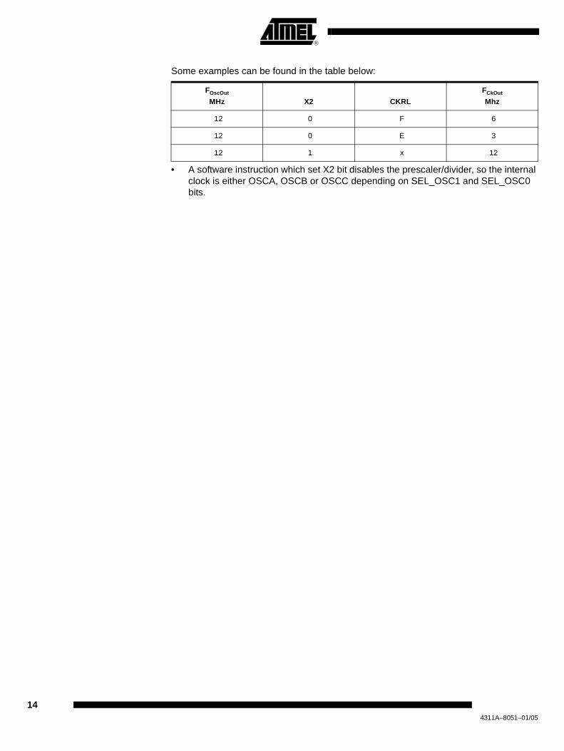
Some examples can be found in the table below:
• A software instruction which set X2 bit disables the prescaler/divider, so the internal clock is either OSCA, OSCB or OSCC depending on SEL_OSC1 and SEL_OSC0 bits.
FOscOut
MHz X2 CKRL
FCkOut
Mhz
12 0 F 6
12 0 E 3
12 1 x 12
144311A–8051–01/05

Registers
Hardware Security Byte The security byte sets the starting microcontroller options and the security levels.
The default options are X1 mode, Oscillator A and divided by 16 prescaler.
Table 2. Hardware Security Byte (HSB)Power configuration Register - HSB (S:EFh)
HSB = 1111 1X11b
7 6 5 4 3 2 1 0
X2 RST_OSC1 RST_OSC0 RST_OCLK CKRLRV - LB1 LB0
Bit
Number
Bit
Mnemonic Description
7 X2X2 ModeClear to force X2 mode (CkOut = OscOut)
Set to use the prescaler mode (CkOut = OscOut / (2*(16-M)))
6 RST_OSC1 Oscillator bit 1 on reset and Oscillator bit 0 on reset
11: allows OSCA10: allows OSCB
01: allows OSCC
00: reserved
5 RST_OSC0
4 RST_OCLK
Output clocking signal after RESET
Clear to start the microcontroller with a low level on P3.5 followed by an output clocking signal on P3.5 as soon as the microcontroller is started. This signal has is a 1/3 high 2/3 low signal. Its frequency is equal to (CKout / 3).
Set to start on normal conditions: No signal on P3.5 which is pulled up.
3 CKRLRV
CKRL Reset Value
If set, the microcontroller starts with the prescaler reset value = XXXX 1000 (OscOut = CkOut/16).
If clear, the microcontroller starts with a prescaler reset value = XXXX 1111 (OscOut = CkOut/2).
2 - Reserved
1-0 LB1-0User Program Lock Bits
See Table 61 on page 81
154311A–8051–01/05

Clock Control Register The clock control register is used to define the clock system behavior.Table 3. OSCON RegisterOSCCON - Clock Control Register (86h)
Reset Value = XXX00"RST_OSC1.RST_OSC0""RST_OSC1.RST_OSC0""RST_OSC1.RST_OSC0" bNot bit addressableNote: Before changing oscillator selection in CKSEL, be sure that the oscillator you select is
started. OSCA is ready as soon as OSCARY is set by hardware, OSCB and OSCC areready after 4 clock periods. In case you want to use OSCB locked, be sure that OSCB isstarted before setting LCKEN bit. Then, wait until OSCBRY is set by hardware to be surethat the accurate frequency is reached.
Oscillator B Frequency Adjust Register
The OSCB Frequency Adjust register is used to adjust the frequency in case of externalcomponents inaccuracies. It allows a frequency variation about 15% around 12 MHzwith a step of around 1%.
7 6 5 4 3 2 1 0
- - OSCARY OSCBRY LCKEN OSCCEN OSCBEN OSCAEN
Bit
Number
Bit
Mnemonic Description
7 -ReservedThe value read from this bit is indeterminate. Do not set this bit.
6 -ReservedThe value read from this bit is indeterminate. Do not set this bit.
5 OSCARYOscillator A Ready
When set, this bit indicates that Oscillator A is ready to be used.
4 OSCBRYOscillator B Ready
When set, this bit indicates that Oscillator B is ready to be used in high accurate mode.
3 LCKENLock Enable
When set, this bit allows to increase the accuracy of OSCB by locking this oscillator on external RC time constant.
2 OSCCEN
Enable low power consumption RC oscillatorThis bit is used to enable the low power consumption oscillator
0: The oscillator is disabled
1: The oscillator is enabled.
1 OSCBEN
Enable high accuracy RC oscillatorThis bit is used to enable the high accurate RC oscillator
0: The oscillator is disabled
1: The oscillator is enabled.
0 OSCAEN
Enable crystal oscillatorThis bit is used to enable the crystal oscillator
0: The oscillator is disabled
1: The oscillator is enabled.
164311A–8051–01/05
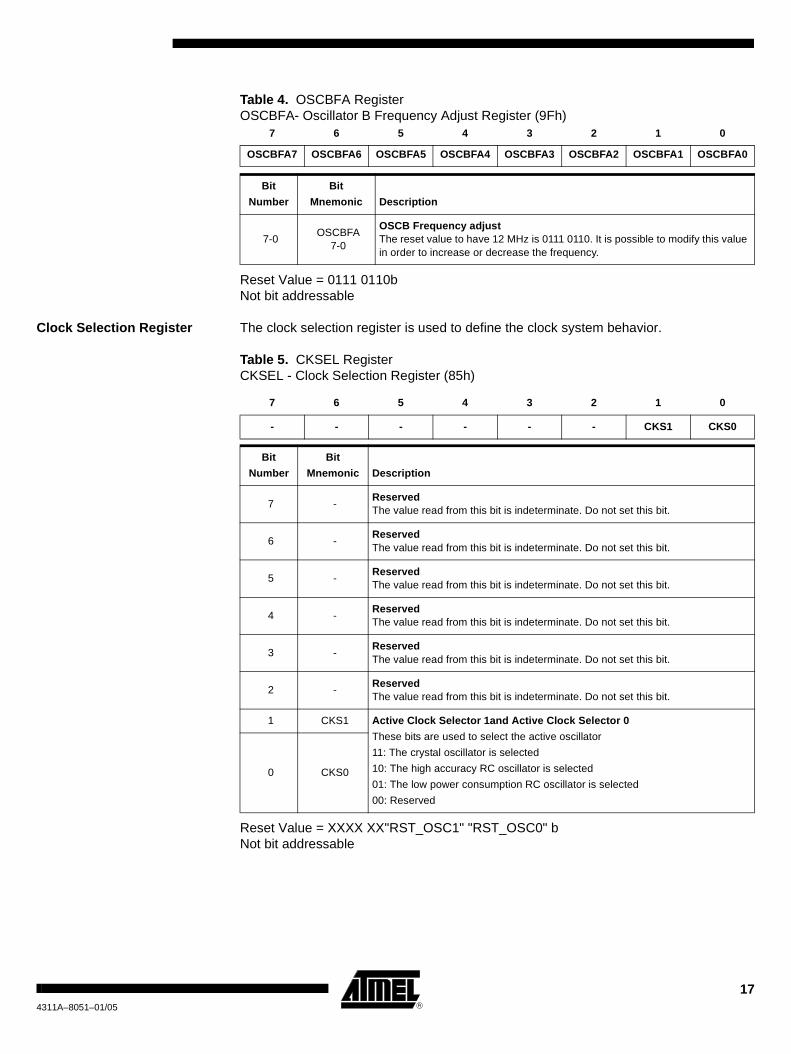
Table 4. OSCBFA RegisterOSCBFA- Oscillator B Frequency Adjust Register (9Fh)
Reset Value = 0111 0110bNot bit addressable
Clock Selection Register The clock selection register is used to define the clock system behavior.
Table 5. CKSEL RegisterCKSEL - Clock Selection Register (85h)
Reset Value = XXXX XX"RST_OSC1" "RST_OSC0" bNot bit addressable
7 6 5 4 3 2 1 0
OSCBFA7 OSCBFA6 OSCBFA5 OSCBFA4 OSCBFA3 OSCBFA2 OSCBFA1 OSCBFA0
Bit
Number
Bit
Mnemonic Description
7-0OSCBFA
7-0
OSCB Frequency adjustThe reset value to have 12 MHz is 0111 0110. It is possible to modify this value in order to increase or decrease the frequency.
7 6 5 4 3 2 1 0
- - - - - - CKS1 CKS0
Bit
Number
Bit
Mnemonic Description
7 -ReservedThe value read from this bit is indeterminate. Do not set this bit.
6 -ReservedThe value read from this bit is indeterminate. Do not set this bit.
5 -ReservedThe value read from this bit is indeterminate. Do not set this bit.
4 -ReservedThe value read from this bit is indeterminate. Do not set this bit.
3 -ReservedThe value read from this bit is indeterminate. Do not set this bit.
2 -ReservedThe value read from this bit is indeterminate. Do not set this bit.
1 CKS1 Active Clock Selector 1and Active Clock Selector 0
These bits are used to select the active oscillator
11: The crystal oscillator is selected
10: The high accuracy RC oscillator is selected
01: The low power consumption RC oscillator is selected
00: Reserved
0 CKS0
174311A–8051–01/05
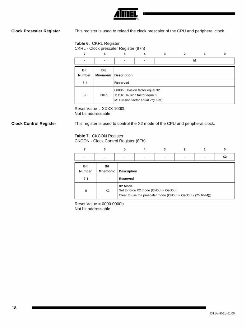
Clock Prescaler Register This register is used to reload the clock prescaler of the CPU and peripheral clock.
Table 6. CKRL RegisterCKRL - Clock prescaler Register (97h)
Reset Value = XXXX 1000bNot bit addressable
Clock Control Register This register is used to control the X2 mode of the CPU and peripheral clock.
Table 7. CKCON RegisterCKCON - Clock Control Register (8Fh)
Reset Value = 0000 0000bNot bit addressable
7 6 5 4 3 2 1 0
- - - - M
Bit
Number
Bit
Mnemonic Description
7-4 - Reserved
3-0 CKRL
0000b: Division factor equal 32
1111b: Division factor equal 2
M: Division factor equal 2*(16-M)
7 6 5 4 3 2 1 0
- - - - - - - X2
Bit
Number
Bit
Mnemonic Description
7-1 - Reserved
0 X2X2 ModeSet to force X2 mode (CkOut = OscOut)
Clear to use the prescaler mode (CkOut = OscOut / (2*(16-M)))
184311A–8051–01/05

Power Modes
Overview As seen in the previous chapter it is possible to modify the AT8xEB5114 clock manage-ment in order to have less consumption.
For applications where power consumption is a critical factor, three power modes areprovided:
• Normal (running) mode
• Idle mode
• Power-down mode
In order to increase ADC accuracy, a Quiet mode also exits. This mode is a pseudo idlemode in which the CPU and all the peripherals except the AD converter are disabled.
Power modes are controlled by PCON SFR register.
Operating Modes Table 8 summarizes all the power modes and states that AT8xEB5114 can encounter. Itshows which parts of AT8xEB5114 are running depending on the operating mode.
Table 8. Operating Modes
Normal Mode In normal mode, the oscillator, the CPU and the peripherals are running. The prescalercan also be activated.
• The CPU and the peripherals clock depends on the software selection using CKCON, OSCCON, CKSEL and CKRL registers
• CKS bits select either OSCA, OSCB, or OSCC
• CKRL register determines the frequency of the selected clock, unless X2 bit is set.In this case the prescaler/divider is not used, so CPU core needs only 6-clock periods per machine cycle.
It is always possible to switch dynamically by software from one to another oscillator bychanging CKS bits, a synchronization cell allows to avoid any spike during transition.
Idle Mode The idle mode allows to reduce consumption by freezing the CPU. All the peripheralscontinue running.
Entering Idle Mode An instruction that sets PCON.0 causes that to be the last instruction executed beforegoing into Idle mode.
In Idle mode, the internal clock signal is gated off to the CPU, but not to the interrupt,and the peripheral functions. The CPU status is entirely preserved: the Stack Pointer,Program Counter, Program Status Word, Accumulator and all other registers maintain
Operating Mode Prescaler Oscillator POR CPU Peripherals
Power Down X
Under Reset A, B or C X
Start X A, B or C X X
Running (X) A, B or C X X X
Idle (X) A, B or C X X
Quiet (X) A, B or C X only ADC
194311A–8051–01/05
their data during Idle. The port pins hold the logical states they had at the time Idle wasactivated. ALE and PSEN are held at logic high levels. The different operating modesare summarized on Table 10 on page 21.
Exit from Idle Mode There are two ways to terminate idle mode. Activation of any enabled interrupt willcause PCON.0 to be cleared by hardware, terminating Idle mode. The interrupt will beserviced, and following RETI the next instruction to be executed will be the one followingthe instruction that put the device into idle. Exit from idle mode will leave the oscillatorscontrol bits on OSCON and CKS registers unchanged.
The flag bits GF0 and GF1 can be used to give an indication if an interrupt occurred dur-ing normal operation or during an Idle mode. For example, an instruction that activatesIdle mode can also set one or both flag bits. When Idle is terminated by an interrupt, theinterrupt service routine can examine the flag bits.
The other way of terminating the Idle mode is with a hardware reset. Since the clockoscillator is still running, the hardware reset needs to be held active for only twomachine cycles (24 oscillator periods) to complete the reset.
In both cases, PCON.0 is cleared by hardware.
Quiet Mode The quiet mode is a pseudo idle mode in which the CPU and all the peripherals exceptthe AD converter are down. For more details, See “Analog-to-Digital Converter (ADC)”on page 57.
Power-down Mode To save maximum power, a power-down mode can be invoked by software (refer toTable 11 on page 22). In power-down mode, the oscillator is stopped and the instructionthat invoked power-down mode is the last instruction executed. The internal RAM andSFRs retain their value until the power-down mode is terminated. VCC can be lowered tosave further power.
Entering Power-down Mode An instruction that sets PCON.1 causes that to be the last instruction executed beforegoing into the power-down mode.
The ports status under power-down is the previous status before entering this powermode.
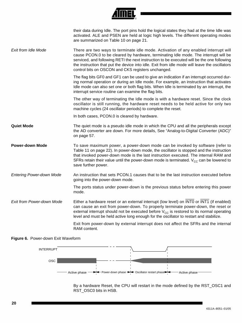
Exit from Power-down Mode Either a hardware reset or an external interrupt (low level) on INT0 or INT1 (if enabled)can cause an exit from power-down. To properly terminate power-down, the reset orexternal interrupt should not be executed before VCC is restored to its normal operatinglevel and must be held active long enough for the oscillator to restart and stabilize.
Exit from power-down by external interrupt does not affect the SFRs and the internalRAM content.
Figure 6. Power-down Exit Waveform
By a hardware Reset, the CPU will restart in the mode defined by the RST_OSC1 andRST_OSC0 bits in HSB.
INTERRUPT
OSC
Power-down phase Oscillator restart phase Active phaseActive phase
204311A–8051–01/05
By INT1 and INT0 interruptions (if enabled), the oscillators control bits on OSCON andCKSEL will be kept, so the selected oscillator before entering in power-down mode willbe activated. Only external interrupts INT0 and INT1 are useful to exit from power-down. Note: Exit from power down mode doesn’t depend on IT0 and IT1 configurations. It is only pos-
sible to exit from power down mode on a low level on these pins.
Holding the pin low restarts the oscillator but bringing the pin high completes the exit asdetailed in Figure 6. When both interrupts are enabled, the oscillator restarts as soon asone of the two inputs is held low and power down exit will be completed when the firstinput is released. In this case the higher priority interrupt service routine is executed.
Table 9 shows the state of ports during idle and power-down modes.
Table 9. Ports State
Mode Program Memory Port3 Port4
Idle Internal Port Data Port Data
Power Down Internal Port Data Port Data
Table 10. Operating Modes
PD IDLE CKS1 CKS0 OSCCEN OSCBEN OSCAEN Selected Mode Comment
0 0 1 1 X X 1 NORMAL MODE A OSCA: XTAL clock
X X 1 1 X X 0 INVALID no active clock
0 0 1 0 X 1 X NORMAL MODE B, OSCB: high accuracy RC clock
X X 1 0 X 0 X INVALID no active clock
0 0 0 1 1 X X NORMAL MODE C, OSCC: low consumption RC clock
X X 0 1 0 X X INVALID no active clock
0 1 1 1 X X 1 IDLE MODE AThe CPU is off, OSCA supplies the peripherals
0 1 1 0 X 1 X IDLE MODE BThe CPU is off, OSCB supplies the peripherals
0 1 0 1 1 X X IDLE MODE CThe CPU is off, OSCC supplies the peripherals
1 X X X X X X POWER DOWNThe CPU is off, OSCA, OSCB and OSCC are stopped
214311A–8051–01/05

Power Modes Control Registers
Table 11. PCON RegisterPCON (S:87h)Power configuration Register
Reset Value = 00XX XX00b
7 6 5 4 3 2 1 0
- - - - GF1 GF0 PD IDL
Bit Number
Bit Mnemonic Description
7 Reserved
6 Reserved
5 Reserved
4 Reserved
3 GF1General Purpose flag 1Set and Cleared by user for general purpose usage.
2 GF0General Purpose flag 0Set and Cleared by user for general purpose usage.
1 PD
Power-down Mode bitCleared by hardware when an interrupt or reset occurs.Set to activate the Power-down mode.If IDL and PD are both set, PD takes precedence.
0 IDL
Idle Mode bitCleared by hardware when an interrupt or reset occurs.Set to activate the Idle mode.If IDL and PD are both set, PD takes precedence.
224311A–8051–01/05

234311A–8051–01/05
AUXR Register
Reset Value = 0XX0 XXXXbNot bit addressable
Table 12. AUXR RegisterAUXR - Auxiliary Register (8Eh)
7 6 5 4 3 2 1 0
DPU - - LOWVD - - - -
Bit
Number
Bit
Mnemonic Description
7 DPUDisable Pull upSet to disable each pull up on all ports.
Clear to connect all pull-ups on each port.
6 -ReservedThe value read from this bit is indeterminate. Do not set this bit.
5 -ReservedThe value read from this bit is indeterminate. Do not set this bit.
4 LOWVDLow Voltage DetectionThis bit is clear by hardware when the supply voltage is under Vpfdp value.
This bit is set by hardware as soon the supply voltage is greater than Vpfdp value.
3-1 -ReservedThe value read from this bit is indeterminate. Do not set this bit.
0 -ReservedThe value read from this bit is indeterminate. Do not set this bit.

Timers/Counters
Introduction The AT8xEB5114 implements two general-purpose, 16-bit Timers/Counters. Althoughthey are identified as Timer 0, Timer 1, they can be independently configured each tooperate in a variety of modes as a Timer or as an event Counter. When operating as aTimer, a Timer/Counter runs for a programmed length of time, then issues an interruptrequest. When operating as a Counter, a Timer/Counter counts negative transitions onan external pin. After a preset number of counts, the Counter issues an interruptrequest.The Timer registers and associated control registers are implemented as addressableSpecial Function Registers (SFRs). Two of the SFRs provide programmable control ofthe Timers as follows:
• Timer/Counter mode control register (TMOD) and Timer/Counter control register (TCON) control both Timer 0 and Timer 1.
The various operating modes of each Timer/Counter are described below.
Timer/Counter Operations
A basic operation is Timer registers THx and TLx (x = 0, 1) connected in cascade toform a 16-bit Timer. Setting the run control bit (TRx) in the TCON register (seeFigure 15) turns the Timer on by allowing the selected input to increment TLx. WhenTLx overflows it increments THx and when THx overflows it sets the Timer overflow flag(TFx) in the TCON register. Setting the TRx does not clear the THx and TLx Timer reg-isters. Timer registers can be accessed to obtain the current count or to enter presetvalues. They can be read at any time but the TRx bit must be cleared to preset their val-ues, otherwise the behavior of the Timer/Counter is unpredictable.
The C/Tx# control bit selects Timer operation or Counter operation by selecting thedivided-down system clock or the external pin Tx as the source for the counted signal.The TRx bit must be cleared when changing the operating mode, otherwise the behaviorof the Timer/Counter is unpredictable.For Timer operation (C/Tx# = 0), the Timer register counts the divided-down systemclock. The Timer register is incremented once every peripheral cycle.
For Counter operation (C/Tx# = 1), the Timer register counts the negative transitions onthe external input pin Tx. The external input is sampled during every S5P2 state. TheProgrammer’s Guide describes the notation for the states in a peripheral cycle. Whenthe sample is high in one cycle and low in the next one, the Counter is incremented. Thenew count value appears in the register during the next S3P1 state after the transitionhas been detected. Since it takes 12 states (24 oscillator periods in X1 mode) to recog-nize a negative transition, the maximum count rate is 1/24 of the oscillator frequency inX1 mode. There are no restrictions on the duty cycle of the external input signal, but toensure that a given level is sampled at least once before it changes, it should be held forat least one full peripheral cycle.
Timer 0 Timer 0 functions as either a Timer or an event Counter in four operating modes.Figure 7 to Figure 10 show the logic configuration of each mode.
Timer 0 is controlled by the four lower bits of the TMOD register (see Figure 16) and bits0, 1, 4 and 5 of the TCON register (see Figure 15). The TMOD register selects themethod of Timer gating (GATE0), Timer or Counter operation (T/C0#) and the operatingmode (M10 and M00). The TCON register provides Timer 0 control functions: overflowflag (TF0), run control bit (TR0), interrupt flag (IE0) and interrupt type control bit (IT0).For normal Timer operation (GATE0= 0), setting TR0 allows TL0 to be incremented bythe selected input. Setting GATE0 and TR0 allows external pin INT0# to control Timer
244311A–8051–01/05

operation.Timer 0 overflow (count rolls over from all 1s to all 0s) sets the TF0 flag and generatesan interrupt request.It is important to stop the Timer/Counter before changing modes.
Mode 0 (13-bit Timer) Mode 0 configures Timer 0 as a 13-bit Timer which is set up as an 8-bit Timer (TH0 reg-ister) with a modulo-32 prescaler implemented with the lower five bits of the TL0 register(see Figure 7). The upper three bits of the TL0 register are indeterminate and should beignored. Prescaler overflow increments the TH0 register.
Figure 7. Timer/Counter x (x= 0 or 1) in Mode 0
Mode 1 (16-bit Timer) Mode 1 configures Timer 0 as a 16-bit Timer with the TH0 and TL0 registers connectedin a cascade (see Figure 8). The selected input increments the TL0 register.
Figure 8. Timer/Counter x (x = 0 or 1) in Mode 1
Mode 2 (8-bit Timer with Auto-Reload)
Mode 2 configures Timer 0 as an 8-bit Timer (TL0 register) that automatically reloadsfrom the TH0 register on overflow (see Figure 9). TL0 overflow sets the TF0 flag in theTCON register and reloads TL0 with the contents of TH0, which is preset by the soft-ware. When the interrupt request is serviced, the hardware clears TF0. The reloadleaves TH0 unchanged. The next reload value may be changed at any time by writing itto the TH0 register.
TRxTCON reg
TFxTCON reg
0
1
GATExTMOD reg
OverflowTimer xInterruptRequest
C/Tx#TMOD reg
TLx(5 bits)
THx(8 bits)
INTx#
Tx
FCkIdle / 6
TRxTCON reg
TFxTCON reg
0
1
GATExTMOD reg
OverflowTimer xInterruptRequest
C/Tx#TMOD reg
TLx(8 bits)
THx(8 bits)
INTx#
Tx
FCkIdle / 6
254311A–8051–01/05

Figure 9. Timer/Counter x (x = 0 or 1) in Mode 2
Mode 3 (Two 8-bit Timers) Mode 3 configures Timer 0 so that registers TL0 and TH0 operate as 8-bit Timers (seeFigure 10). This mode is provided for applications requiring an additional 8-bit Timer orCounter. TL0 uses the Timer 0 control bits C/T0# and GATE0 in the TMOD register, andTR0 and TF0 in the TCON register in the normal manner. TH0 is locked into a Timerfunction (counting FUART) and takes over use of the Timer 1 interrupt (TF1) and run con-trol (TR1) bits. Thus, operation of Timer 1 is restricted when Timer 0 is in mode 3.
Figure 10. Timer/Counter 0 in Mode 3: Two 8-bit Counters
Timer 1 Timer 1 is identical to Timer 0 except for Mode 3 which is a hold-count mode. The fol-lowing comments help to understand the differences:
• Timer 1 functions as either a Timer or an event Counter in the three operating modes. Figure 7 to Figure 9 show the logical configuration for modes 0, 1, and 2. Mode 3 of Timer 1 is a hold-count mode.
• Timer 1 is controlled by the four high-order bits of the TMOD register (see Figure 16) and bits 2, 3, 6 and 7 of the TCON register (see Figure 15). The TMOD register selects the method of Timer gating (GATE1), Timer or Counter operation (C/T1#) and the operating mode (M11 and M01). The TCON register provides Timer 1 control functions: overflow flag (TF1), run control bit (TR1), interrupt flag (IE1) and the interrupt type control bit (IT1).
• Timer 1 can serve as the Baud Rate Generator for the Serial Port. Mode 2 is best suited for this purpose.
TRxTCON reg
TFxTCON reg
0
1
GATExTMOD reg
OverflowTimer xInterruptRequest
C/Tx#TMOD reg
TLx(8 bits)
THx(8 bits)
INTx#
Tx
FCkIdle / 6
TR0TCON.4
TF0TCON.5
INT0#
0
1
GATE0TMOD.3
OverflowTimer 0InterruptRequest
C/T0#TMOD.2
TL0(8 bits)
TR1TCON.6
TH0(8 bits) TF1
TCON.7
OverflowTimer 1InterruptRequest
T0
FCkIdle
FCkIdle
/ 6
264311A–8051–01/05
• For normal Timer operation (GATE1= 0), setting TR1 allows TL1 to be incremented by the selected input. Setting GATE1 and TR1 allows external pin INT1# to control Timer operation.
• Timer 1 overflow (count rolls over from all 1s to all 0s) sets the TF1 flag and generates an interrupt request.
• When Timer 0 is in mode 3, it uses Timer 1’s overflow flag (TF1) and run control bit (TR1). For this situation, use Timer 1 only for applications that do not require an interrupt (such as a Baud Rate Generator for the Serial Port) and switch Timer 1 in and out of mode 3 to turn it off and on.
• It is important to stop the Timer/Counter before changing modes.
Mode 0 (13-bit Timer) Mode 0 configures Timer 1 as a 13-bit Timer, which is set up as an 8-bit Timer (TH1 reg-ister) with a modulo-32 prescaler implemented with the lower 5 bits of the TL1 register(see Figure 7). The upper 3 bits of TL1 register are indeterminate and should beignored. Prescaler overflow increments the TH1 register.
Mode 1 (16-bit Timer) Mode 1 configures Timer 1 as a 16-bit Timer with TH1 and TL1 registers connected incascade (see Figure 8). The selected input increments the TL1 register.
Mode 2 (8-bit Timer with Auto-Reload)
Mode 2 configures Timer 1 as an 8-bit Timer (TL1 register) with automatic reload fromthe TH1 register on overflow (see Figure 9). TL1 overflow sets the TF1 flag in the TCONregister and reloads TL1 with the contents of TH1, which is preset by the software. Thereload leaves TH1 unchanged.
Mode 3 (Halt) Placing Timer 1 in mode 3 causes it to halt and hold its count. This can be used to haltTimer 1 when the TR1 run control bit is not available i.e. when Timer 0 is in mode 3.
274311A–8051–01/05

Registers Table 13. TCON (S:88h)Timer/Counter Control Register
Reset Value = 0000 0000b
7 6 5 4 3 2 1 0
TF1 TR1 TF0 TR0 IE1 IT1 IE0 IT0
Bit Number
Bit Mnemonic Description
7 TF1Timer 1 Overflow flagCleared by the hardware when processor vectors to interrupt routine.Set by the hardware on Timer 1 register overflows.
6 TR1Timer 1 Run Control bitClear to turn off Timer/Counter 1.Set to turn on Timer/Counter 1.
5 TF0Timer 0 Overflow flagCleared by the hardware when processor vectors to interrupt routine.Set by the hardware on Timer 0 register overflows.
4 TR0Timer 0 Run Control bitClear to turn off Timer/Counter 0.Set to turn on Timer/Counter 0.
3 IE1Interrupt 1 Edge flagCleared by the hardware as soon as the interrupt is processed.Set by the hardware when external interrupt is detected on the INT1 pin.
2 IT1
Interrupt 1 Type Control bitClear to select low level active for external interrupt 1 (INT1).Set to select sensitive edge trigger for external interrupt 1. The sensitive edge (Rising or Falling) is determined by ESB1 value (Edge Selection Bit 1) in IOR (Interrupt Option Register).
1 IE0Interrupt 0 Edge flagCleared by the hardware as soon as the interrupt is processed.Set by the hardware when external interrupt is detected on INT0 pin.
0 IT0
Interrupt 0 Type Control bitClear to select low level active trigger for external interrupt 0 (INT0).Set to select sensitive edge trigger for external interrupt 0. The sensitive edge (Rising or Falling) is determined by ESB0 (Edge Selection Bit 0) in IOR (Interrupt Option Register).
284311A–8051–01/05

Table 14. IOR (S:A5h)Interrupt Option Register.
Reset Value = XXXX XX00b
7 6 5 4 3 2 1 0
- - - - - - ESB1 ESB0
Bit Number
Bit Mnemonic Description
7-2 -Reserved
The value read from this bit is indeterminate. Do not set this bit.
1 ESB1
Edge Selection bit for INT1
Clear to select falling edge sensitive for INT1 pin.
Set to select rising edge sensitive for INT1 pin.
0 ESB0Edge Selection bit for INT0Clear to select falling edge sensitive for INT0 pin.
Set to select rising edge sensitive for INT0 pin.
294311A–8051–01/05

Table 15. TMOD RegisterTMOD (S:89h)Timer/Counter Mode Control Register.
Reset Value = 0000 0000b
Table 16. TH0 Register
TH0 (S:8Ch)Timer 0 High Byte Register.
Reset Value = 0000 0000b
7 6 5 4 3 2 1 0
GATE1 C/T1# M11 M01 GATE0 C/T0# M10 M00
Bit Number
Bit Mnemonic Description
7 GATE1Timer 1 Gating Control bitClear to enable Timer counter 1 whenever TR1 bit is set.Set to enable Timer counter 1 only while INT1# pin is high and TR1 bit is set.
6 C/T1#Timer 1 Counter/Timer Select bitClear for Timer operation: Timer 1 counts the divided-down system clock.Set for Counter operation: Timer 1 counts negative transitions on external pin T1.
5 M11 Timer 1 Mode Select bitsM11 M01 Operating mode 0 0 Mode 0: 8-bit Timer/Counter (TH1) with 5-bit prescaler (TL1). 0 1 Mode 1: 16-bit Timer/Counter. 1 0 Mode 2: 8-bit auto-reload Timer/Counter (TL1). Reloaded from
TH1 at overflow. 1 1 Mode 3:Timer 1 halted. Retains count.
4 M01
3 GATE0Timer 0 Gating Control bitClear to enable Timer counter 0 whenever TR0 bit is set.Set to enable Timer counter 0 only while INT0# pin is high and TR0 bit is set.
2 C/T0#Timer 0 Counter/Timer Select bitClear for Timer operation: Timer 0 counts the divided-down system clock.Set for Counter operation: Timer 0 counts negative transitions on external pin T0.
1 M10 Timer 0 Mode Select bitM10 M00 Operating mode 0 0 Mode 0:8-bit Timer/Counter (TH0) with 5-bit prescaler (TL0). 0 1 Mode 1:16-bit Timer/Counter. 1 0 Mode 2:8-bit auto-reload Timer/Counter (TL0).
Reloaded from TH0 at overflow 1 1 Mode 3:TL0 is an 8-bit Timer/CounterTH0 is an 8-bit Timer using Timer 1’s TR0 and TF0 bits.
0 M00
7 6 5 4 3 2 1 0
Bit Number
Bit Mnemonic Description
7:0 High Byte of Timer 0.
304311A–8051–01/05

Table 17. TL0 Register
TL0 (S:8Ah)
Timer 0 Low Byte Register.
Reset Value = 0000 0000b
Table 18. TH1 Register
TH1 (S:8Dh)Timer 1 High Byte Register.
Reset Value = 0000 0000b
Table 19. TL1 Register
TL1 (S:8Bh)Timer 1 Low Byte Register.
Reset Value = 0000 0000b
7 6 5 4 3 2 1 0
Bit Number
Bit Mnemonic Description
7:0 Low Byte of Timer 0.
7 6 5 4 3 2 1 0
Bit Number
Bit Mnemonic Description
7:0 High Byte of Timer 1.
7 6 5 4 3 2 1 0
Bit Number
Bit Mnemonic Description
7:0 Low Byte of Timer 1.
314311A–8051–01/05

Ports The AT8xEB5114 has 2 I/O ports, port 3, and port 4.
All port3 and port4 I/O port pins on the AT8xEB5114 may be software configured to oneof four types on a bit-by-bit basis, as shown below in Table 20. These are: quasi-bidirec-tional (standard 80C51 port outputs), push-pull, open drain, and input only. Twoconfiguration registers for each port select the output type for each port pin.
Table 20. Port Output Configuration setting using PxM1 and PxM2 registers (3< x < 4)
Port Types
Quasi-Bidirectional Output Configuration
The default port output configuration for standard AT8xEB5114 I/O ports is the quasi-bidirectional output that is common on the 80C51 and most of its derivatives. This outputtype can be used as both an input and output without the need of reconfiguring the port.This is possible because when the port outputs a logic high, it is weakly driven, allowingan external device to pull the pin low. When the pin is pulled low, it is driven strongly andable to sink a fairly large current. These features are somewhat similar to an open drainoutput except that there are three pull-up transistors in the quasi-bidirectional output thatserve different purposes. One of these pull-ups, called the "weak" pull-up, is turned onwhenever the port latch for the pin contains a logic 1. The weak pull-up sources a verysmall current that will pull the pin high if it is left floating. A second pull-up, called the"medium" pull-up, is turned on when the port latch for the pin contains a logic 1 and thepin itself is also at a logic 1 level. This pull-up provides the primary source current for aquasi-bidirectional pin that is outputting a 1. If a pin that has a logic 1 on it is pulled lowby an external device, the medium pull-up turns off, and only the weak pull-up remainson. In order to pull the pin low under these conditions, the external device has to sinkenough current to overpower the medium pull-up and take the voltage on the port pinbelow its input threshold.
The third pull-up is referred to as the "strong" pull-up. This pull-up is used to speed uplow-to-high transitions on a quasi-bidirectional port pin when the port latch changes froma logic 0 to a logic 1. When this occurs, the strong pull-up turns on for a brief time, twoCPU clocks, in order to pull the port pin high quickly. Then it turns off again.
The quasi-bidirectional port configuration is shown in Figure 11.
PxM1.(2y+1) bit PxM1.(2y) bit (0<y<3) Port Output Mode
0 0 Quasi bidirectional
0 1 Push-Pull
1 0 Input Only (High Impedance)
1 1 Open Drain
PxM2.(2y-7) bit PxM2.(2y-8) bit (4<y<7) Port Output Mode
0 0 Quasi bidirectional
0 1 Push-Pull
1 0 Input Only (High Impedance)
1 1 Open Drain
324311A–8051–01/05
Figure 11. Quasi-Bidirectional Output
Open Drain Output Configuration
The open drain output configuration turns off all pull-ups and only drives the pull-downtransistor of the port driver when the port latch contains a logic 0. To be used as a logicoutput, a port configured in this manner must have an external pull-up, typically a resis-tor tied to VDD. The pull-down for this mode is the same as the quasi-bidirectional mode.The open drain port configuration is shown in Figure 12.
Figure 12. Open Drain Output
Push-Pull Output Configuration
The push-pull output configuration has the same pull-down structure as both the opendrain and the quasi-bidirectional output modes, but provides a continuous strong pull-upwhen the port latch contains a logic 1. The push-pull mode may be used when moresource current is needed from a port output. The push-pull port configuration is shown inFigure 13.
2 CPU
Input
Pin
Strong Medium
N
P PWeak
PCLOCK DELAY
Port Latch
Data
Data
DPUAUXR.7
Input
PinNPort latch
Data
Data
334311A–8051–01/05
Figure 13. Push-Pull Output
Input only Configuration The input only configuration is a pure input with neither pull-up nor pull-down.
The input only configuration is shown in Figure 13.
Figure 14. Input only
Ports Description
Ports P3 and P4 The inputs of each I/O port of the AT8xEB5114 are TTL level Schmitt triggers withhysteresis.
Input
Pin
Strong
N
P
Port latch
Data
Data
Input
PinData
344311A–8051–01/05
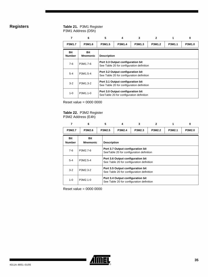
Registers Table 21. P3M1 RegisterP3M1 Address (D5h)
Reset value = 0000 0000
Table 22. P3M2 RegisterP3M2 Address (E4h)
Reset value = 0000 0000
7 6 5 4 3 2 1 0
P3M1.7 P3M1.6 P3M1.5 P3M1.4 P3M1.3 P3M1.2 P3M1.1 P3M1.0
Bit Number
Bit Mnemonic Description
7-6 P3M1.7-6Port 3.3 Output configuration bit See Table 20 for configuration definition
5-4 P3M1.5-4Port 3.2 Output configuration bit See Table 20 for configuration definition
3-2 P3M1.3-2Port 3.1 Output configuration bit See Table 20 for configuration definition
1-0 P3M1.1-0Port 3.0 Output configuration bit SeeTable 20 for configuration definition
7 6 5 4 3 2 1 0
P3M2.7 P3M2.6 P3M2.5 P3M2.4 P3M2.3 P3M2.2 P3M2.1 P3M2.0
Bit
Number
Bit
Mnemonic Description
7-6 P3M2.7-6Port 3.7 Output configuration bit SeeTable 20 for configuration definition
5-4 P3M2.5-4Port 3.6 Output configuration bit See Table 20 for configuration definition
3-2 P3M2.3-2Port 3.5 Output configuration bit See Table 20 for configuration definition
1-0 P3M2.1-0Port 3.4 Output configuration bit See Table 20 for configuration definition
354311A–8051–01/05
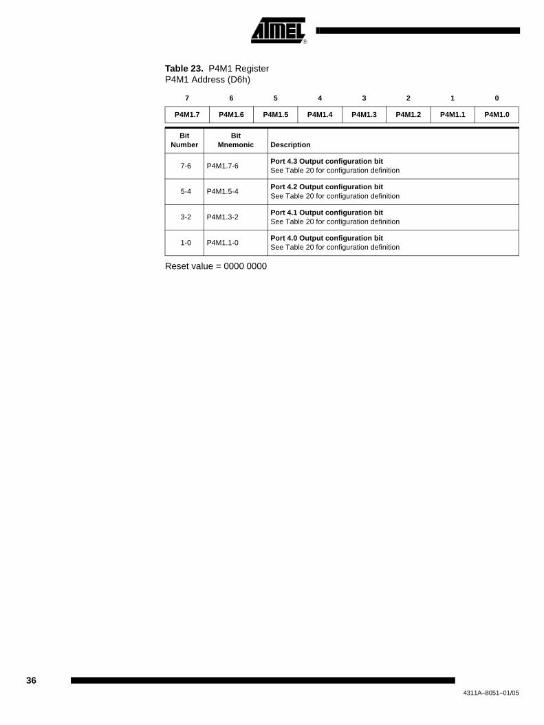
Table 23. P4M1 RegisterP4M1 Address (D6h)
Reset value = 0000 0000
7 6 5 4 3 2 1 0
P4M1.7 P4M1.6 P4M1.5 P4M1.4 P4M1.3 P4M1.2 P4M1.1 P4M1.0
Bit Number
Bit Mnemonic Description
7-6 P4M1.7-6Port 4.3 Output configuration bit See Table 20 for configuration definition
5-4 P4M1.5-4Port 4.2 Output configuration bit See Table 20 for configuration definition
3-2 P4M1.3-2Port 4.1 Output configuration bit See Table 20 for configuration definition
1-0 P4M1.1-0Port 4.0 Output configuration bit See Table 20 for configuration definition
364311A–8051–01/05

Dual Data Pointer Register (DDPTR)
The additional data pointer can be used to speed up code execution and reduce codesize in a number of ways.
The dual DPTR structure is a way by which the chip will specify the address of an exter-nal data memory location. There are two 16-bit DPTR registers that address the externalmemory, and a single bit called DPS = AUXR1/bit0 (See Figure 15) that allows the pro-gram code to switch between them.
Figure 15. Use of Dual Pointer
External Data Memory
AUXR1(A2H)
DPS
DPH(83H) DPL(82H)
07
DPTR0
DPTR1
374311A–8051–01/05
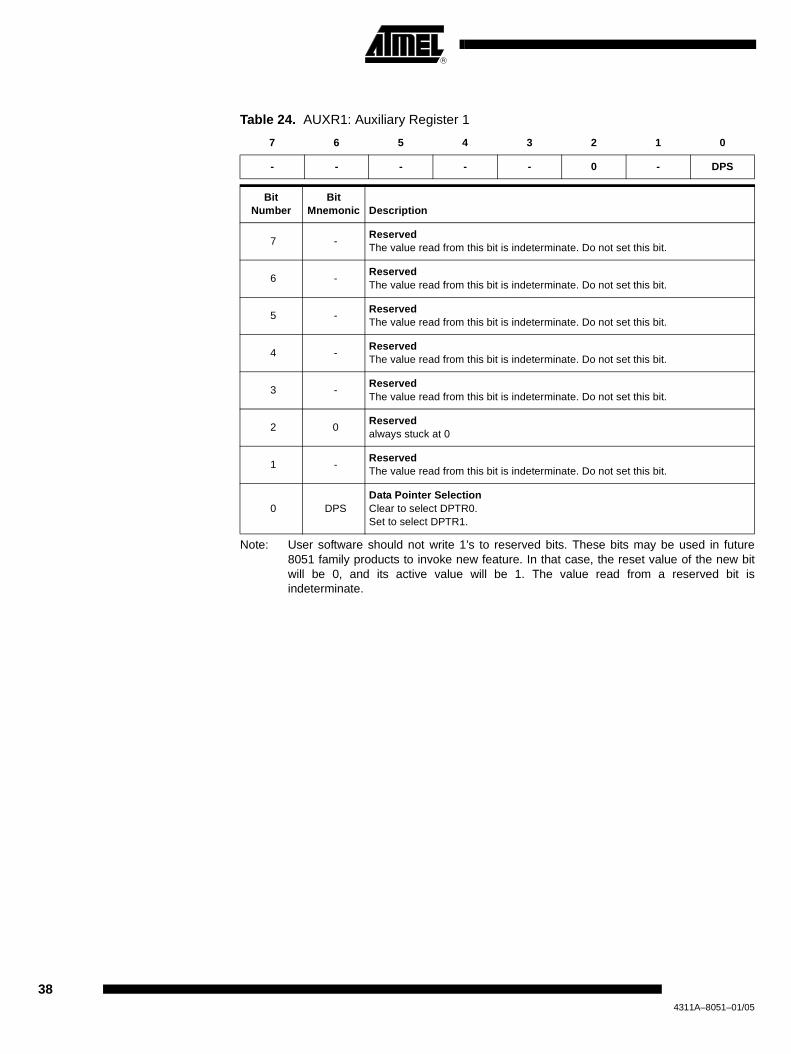
Note: User software should not write 1’s to reserved bits. These bits may be used in future8051 family products to invoke new feature. In that case, the reset value of the new bitwill be 0, and its active value will be 1. The value read from a reserved bit isindeterminate.
Table 24. AUXR1: Auxiliary Register 1
7 6 5 4 3 2 1 0
- - - - - 0 - DPS
Bit Number
Bit Mnemonic Description
7 -ReservedThe value read from this bit is indeterminate. Do not set this bit.
6 -ReservedThe value read from this bit is indeterminate. Do not set this bit.
5 -ReservedThe value read from this bit is indeterminate. Do not set this bit.
4 -ReservedThe value read from this bit is indeterminate. Do not set this bit.
3 -ReservedThe value read from this bit is indeterminate. Do not set this bit.
2 0Reservedalways stuck at 0
1 -ReservedThe value read from this bit is indeterminate. Do not set this bit.
0 DPSData Pointer SelectionClear to select DPTR0.Set to select DPTR1.
384311A–8051–01/05

Application Software can take advantage of the additional data pointers to both increase speed andreduce code size, for example, block operations (copy, compare, search...) are wellserved by using one data pointer as a ’source’ pointer and the other one as a ‘destina-tion’ pointer.
ASSEMBLY LANGUAGE
; Block move using dual data pointers ; Destroys DPTR0, DPTR1, A and PSW ; note: DPS exits opposite of entry state ; unless an extra INC AUXR1 is added ; 00A2 AUXR1 EQU 0A2H ; 0000 909000MOV DPTR,#SOURCE ; address of SOURCE 0003 05A2 INC AUXR1 ; switch data pointers 0005 90A000 MOV DPTR,#DEST ; address of DEST 0008 LOOP: 0008 05A2 INC AUXR1 ; switch data pointers 000A E0 MOVX A,@DPTR ; get a byte from SOURCE 000B A3 INC DPTR ; increment SOURCE address 000C 05A2 INC AUXR1 ; switch data pointers 000E F0 MOVX @DPTR,A ; write the byte to DEST 000F A3 INC DPTR ; increment DEST address 0010 70F6JNZ LOOP ; check for 0 terminator 0012 05A2 INC AUXR1 ; (optional) restore DPS
INC is a short (2 bytes) and fast (12 clocks) way to manipulate the DPS bit in the AUXR1SFR. However, note that the INC instruction does not directly force the DPS bit to a par-ticular state, but simply toggles it. In simple routines, such as the block move example,only the fact that DPS is toggled in the proper sequence matters, not its actual value. Inother words, the block move routine works the same whether DPS is '0' or '1' on entry.Observe that without the last instruction (INC AUXR1), the routine will exit with DPS inthe opposite state.
394311A–8051–01/05
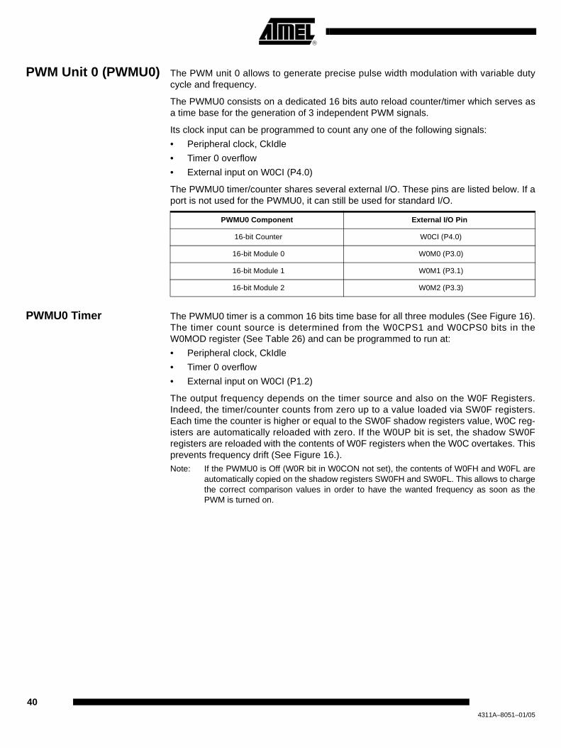
PWM Unit 0 (PWMU0) The PWM unit 0 allows to generate precise pulse width modulation with variable dutycycle and frequency.
The PWMU0 consists on a dedicated 16 bits auto reload counter/timer which serves asa time base for the generation of 3 independent PWM signals.
Its clock input can be programmed to count any one of the following signals:
• Peripheral clock, CkIdle
• Timer 0 overflow
• External input on W0CI (P4.0)
The PWMU0 timer/counter shares several external I/O. These pins are listed below. If aport is not used for the PWMU0, it can still be used for standard I/O.
PWMU0 Timer The PWMU0 timer is a common 16 bits time base for all three modules (See Figure 16).The timer count source is determined from the W0CPS1 and W0CPS0 bits in theW0MOD register (See Table 26) and can be programmed to run at:
• Peripheral clock, CkIdle
• Timer 0 overflow
• External input on W0CI (P1.2)
The output frequency depends on the timer source and also on the W0F Registers.Indeed, the timer/counter counts from zero up to a value loaded via SW0F registers.Each time the counter is higher or equal to the SW0F shadow registers value, W0C reg-isters are automatically reloaded with zero. If the W0UP bit is set, the shadow SW0Fregisters are reloaded with the contents of W0F registers when the W0C overtakes. Thisprevents frequency drift (See Figure 16.).Note: If the PWMU0 is Off (W0R bit in W0CON not set), the contents of W0FH and W0FL are
automatically copied on the shadow registers SW0FH and SW0FL. This allows to chargethe correct comparison values in order to have the wanted frequency as soon as thePWM is turned on.
PWMU0 Component External I/O Pin
16-bit Counter W0CI (P4.0)
16-bit Module 0 W0M0 (P3.0)
16-bit Module 1 W0M1 (P3.1)
16-bit Module 2 W0M2 (P3.3)
404311A–8051–01/05

Figure 16. PWMU0 Timer/Counter
Table 25. W0CON: PWMU0 Control registerW0CON - PWMU0 Control Register (E8h)
Reset Value = 00XX 0000bBit addressable
7 6 5 4 3 2 1 0
W0UP W0R - - W0OS W0EN2 W0EN1 W0EN0
Bit
Number
Bit
Mnemonic Description
7 W0UPPWMU0 update bit
Set by software to request the load of all shadow registers on the next overtaking of the W0C counter. Reset by hardware after the loading of the shadow registers.
6 W0RPWMU0 Run control bit
Set by software to turn the PWMU0 counter on. Must be cleared by software to turn the PWMU0 counter off.
5-4 - Not used
3 W0OS
Pin W0M1 PWMU0 Output Selection
0 W0M1 is PWM module 1 XOR PWM module2 output
1 W0M1 is PWM module 1 output
2 W0EN2PWMU0 Module 2 enable bit
Enable PWMU0 module 2 if set.
1 W0EN1PWMU0 Module 1 enable bit
Enable PWMU0 module 1if set.
0 W0EN0PWMU0 Module 0 enable bit
Enable PWMU0 module 0 if set.
W0EN2 W0EN1 W0EN0
W0CH W0CL
To PWMU0modules
FCkIdle
T0 OVF
W0CI
W0CON
SW0FH SW0FL
W0OS1W0RW0UP
16 bit up
W0INV2 W0INV1 W0INV0W0MODWOPS0W0PS1
W0FH W0FL
0000 0000
16 bit comparator ≥
counter
overtaking
414311A–8051–01/05

Table 26. W0MOD: PWMU0 Counter Mode RegisterW0MOD - PWMU0 Counter Mode Register (E9h)
Reset Value = 00XX X000bNot bit addressable
Because they use the same timer, all three modules have the same frequency deter-mined by the shadow SW0F registers.
Table 27. W0FH: PWMU0 frequency high control registerW0FH - PWMU0 Frequency Control Register (EAh)
Reset Value = 1111 1111bNot bit addressable
7 6 5 4 3 2 1 0
W0CPS1 W0CPS0 - - - W0INV2 W0INV1 W0INV0
Bit
Number
Bit
Mnemonic Description
7 W0CPS1 PWMU0 Count Pulse Select bit1
6 W0CPS0
PWMU0 Count Pulse Select bit0
CPS1 CPS0 Selected PWMU0 input
00 Internal clock fCkIdle
01 Reserved
10 Timer 0 Overflow
11 External clock input on W0CI at max rate = fCkIdle/4
5-3 - Not used
2 W0INV2PWMU0 Module 2 inverter bit
Select the output PWM mode. If set, PWM module 2 output starts with high level.
1 W0INV1PWMU0 Module 1 inverter bit
Select the output PWM mode. If set, PWM module 1 output starts with high level.
0 W0INV0PWMU0 Module 0 inverter bit
Select the output PWM mode. If set, PWM module 0 output starts with high level.
7 6 5 4 3 2 1 0
W0F15 W0F14 W0F13 W0F12 W0F11 W0F10 W0F9 W0F8
Bit
Number
Bit
Mnemonic Description
7-0 W0F15-8PWMU0 high bits counter control frequency
The PWMU0 counter is counting from zero up to W1F15-0 value.
424311A–8051–01/05

Table 28. W0FL: PWMU0 frequency low control registerW0FL - PWMU0 Frequency Control Register (EBh)
Reset Value = 1111 1111bNot bit addressable
Table 29. W0CH: PWMU0 counter high control registerW0CH - PWMU0 Counter Control Register (ECh)
Reset Value = 0000 0000bNot bit addressable
Table 30. W0CL: PWMU0 counter low control registerW0CL - PWMU0 Counter Control Register (EDh)
Reset Value = 0000 0000bNot bit addressable
PWMU0 Output Generation
All the PWMU0 modules have the same frequency determined by the W0F register. Buteach module has its own duty cycle determined by the W0Rn Register. (n is the modulenumber).
When the W0C content is lower than the value programmed via the W0Rn registers, theoutput is the W0INVn-bit (low if 0, high if 1). When it is equal or higher, the output is theopposite of this W0INVn-bit (high if 0, low if 1).
When the W0C content is higher than SW0F’s, an overtaking occurs. The counter value(W0C registers) is automatically reloaded with zero (see Figure 16). If the W0UP bit ishigh, the new comparison value is reloaded on the shadow SW0R0 registers with the
7 6 5 4 3 2 1 0
W0F7 W0F6 W0F5 W0F4 W0F3 W0F2 W0F1 W0F0
Bit
Number
Bit
Mnemonic Description
7-0 W0F7-0PWMU0 low bits counter control frequency
The PWMU0 counter is counting from zero up to WOF15-0 value.
7 6 5 4 3 2 1 0
W0C15 W0C14 W0C13 W0C12 W0C11 W0C10 W0C9 W0C8
Bit
Number
Bit
Mnemonic Description
7-0 W0C15-8 PWMU0 high bits counter frequency.
7 6 5 4 3 2 1 0
W0C7 W0C6 W0C5 W0C4 W0C3 W0C2 W0C1 W0C0
Bit
Number
Bit
Mnemonic Description
7-0 W0C7-0 PWMU0 low bits counter frequency.
434311A–8051–01/05

content of the W0R0 registers (see Figure 16). This method allows to change frequencyand duty cycle without glitch.Note: If the PWMU0 is off (W0R bit in W0CON not set), W0RnH and W0RnL contents are auto-
matically copied on the shadow registers SW0RnH and SW0RnLn and the contents ofW0FH and W0FL are automatically copied on the shadow registers SW0FH and SW0FL.This allows to charge the correct comparison values for each PWM module as soon asthe PWMU0 timer/counter is turned on.
Figure 17. PWMU0 Interrupt System
The W0INVn bits that allow output inversion are on the W0MOD (W0 Counter Mode)register (See Table 26.).
Table 31. W0RnH: PWMU0 module n High Toggle RegisterW0R0H - PWMU0 Module 0 High Toggle Register (D9h)W0R1H - PWMU0 Module 1 High Toggle Register (DBh)W0R2H - PWMU0 Module 2 High Toggle Register (DDh)
Reset Value = 0000 0000bNot bit addressable
7 6 5 4 3 2 1 0
W0RnH15 W0RnH14 W0RnH13 W0RnH12 W0RnH11 W0RnH10 W0RnH9 W0RnH8
Bit
Number
Bit
Mnemonic Description
7-0W0RnH
15-8PWMU0 Module n high toggle register
When the counter exceeds this value, module n output toggles.
W0CH W0CL
SW0RnH SW0RnL
W0RnH W0RnL
16 bits-comparator Š<
overtaking
Module n output
W0INVnW0UP
444311A–8051–01/05
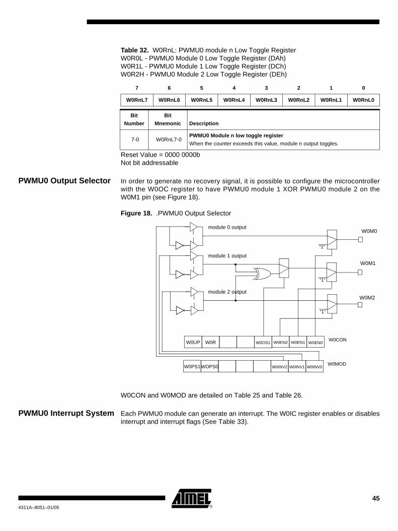
Table 32. W0RnL: PWMU0 module n Low Toggle RegisterW0R0L - PWMU0 Module 0 Low Toggle Register (DAh)W0R1L - PWMU0 Module 1 Low Toggle Register (DCh)W0R2H - PWMU0 Module 2 Low Toggle Register (DEh)
Reset Value = 0000 0000bNot bit addressable
PWMU0 Output Selector In order to generate no recovery signal, it is possible to configure the microcontrollerwith the W0OC register to have PWMU0 module 1 XOR PWMU0 module 2 on theW0M1 pin (see Figure 18).
Figure 18. .PWMU0 Output Selector
W0CON and W0MOD are detailed on Table 25 and Table 26.
PWMU0 Interrupt System Each PWMU0 module can generate an interrupt. The W0IC register enables or disablesinterrupt and interrupt flags (See Table 33).
7 6 5 4 3 2 1 0
W0RnL7 W0RnL6 W0RnL5 W0RnL4 W0RnL3 W0RnL2 W0RnL1 W0RnL0
Bit
Number
Bit
Mnemonic Description
7-0 W0RnL7-0PWMU0 Module n low toggle register
When the counter exceeds this value, module n output toggles.
W0M0 module 0 output
W0M1 module 1 output
module 2 outputW0M2
W0EN2 W0EN1 W0EN0W0CON
W0OS1W0RW0UP
W0INV2 W0INV1 W0INV0W0MODWOPS0W0PS1
“1”
“1”
“1”
454311A–8051–01/05
Figure 19. PWMU0 Interrupt Configuration
Table 33. PWMU0 interrupt control registerW0IC - PWMU0 Interrupt Control Register (EEh)
Reset Value = 0000 0000bNot bit addressable
7 6 5 4 3 2 1 0
W0CF W0CF2 W0CF1 W0CF0 W0ECOF W0ECF2 W0ECF1 W0ECF0
Bit
Number
Bit
Mnemonic Description
7 W0COF
PWMU0 Counter Overtaking Flag
Set by hardware when the counter is higher or equal to SW0F’s value. CF flags an interrupt if bit W0ECOF is set. W0COF can be set either by hardware or software but can only be cleared by software.
6 W0CF2PWMU0 Module 2 Toggle flag
Set by hardware when a match occurs. Can also be set by software. Must be cleared by software.
5 W0CF1PWMU0 Module 1 Toggle flag
Set by hardware when a match occurs. Can also be set by software. Must be cleared by software.
4 W0CF0PWMU0 Module 0 Toggle flag
Set by hardware when a match occurs. Can also be set by software. Must be cleared by software.
3 W0ECOFPWMU0 Counter Overtaking flag
Set to Enable IT on PWMU0 Counter Overtaking Flag.
2 W0ECF2PWMU0 Module 2 Counter flag
Set to enable IT on PWMU0 Module 2 Toggle flag.
1 W0ECF1PWMU0 Module 1 Counter flag
Set to enable IT on PWMU0 Module 1Toggle flag.
0 W0ECF0PWMU0 Module 0 Counter flag
Set to enable IT on PWMU0 Module 0Toggle flag.
W0 W0 W0 W0
Module 2
Module 1
IE0.4 IE0.7
To Interruptpriority decoder
EW0 EACF1 CF0 ECF1 ECF0
W0CF2
W0COF
Module 0
Overtaking
W0 W0ECOF ECF2
W0IC
464311A–8051–01/05

PWM Unit 1 (PWMU1) The PWM unit 1 allows to generate precise pulse width modulation with variable dutycycle and frequency.
The PWMU1 consists of a dedicated 16 bits auto reload counter/timer which serves as atime base for the generation of an independent PWM signal.
Its clock input can be programmed to count any one of the following signals:
• Peripheral clock, CkIdle
• Timer 1 overflow
• External input on W1CI (P4.2)
The PWMU1 timer/counter shares two external I/O. These pins are listed below. If a portis not used for the PWMU1, it can still be used for standard I/O.
PWMU1 Timer The PWMU1 timer is a 16-bit timer (See Figure 20). The timer count source is deter-mined from the W1CPS1 and W1CPS0 bits in the W1CON register (See Table 34) andcan be programmed to run at:
• Peripheral clock, CkIdle
• Timer 1 overflow
• External input on W1CI (P4.2)
The output frequency depends on the timer source and also on the W1F Registers. Thetimer/counter counts from zero up to a value loaded via SW1F registers. Each time thecounter is higher or equal to the SW1F shadow registers value, W1C registers are auto-matically reloaded with zero. If the W1UP bit is set, the shadow SW1F registers isreloaded with the contents of W1F registers when W1C overtakes. This allows to pre-vent frequency drift (See Figure 20).Note: If the PWMU1 is Off (W1R bit in W1CON not set), the contents of W1FH and W1FL are
automatically copied on the shadow registers SW1FH and SW1FL. This allows to chargethe correct comparison values in order to have the desired frequency as soon as thePWM is turned on.
PWMU1 Component External I/O Pin
16-bit Counter W1CI (P4.2)
16-bit Module 0 W1M0 (P3.5)
474311A–8051–01/05
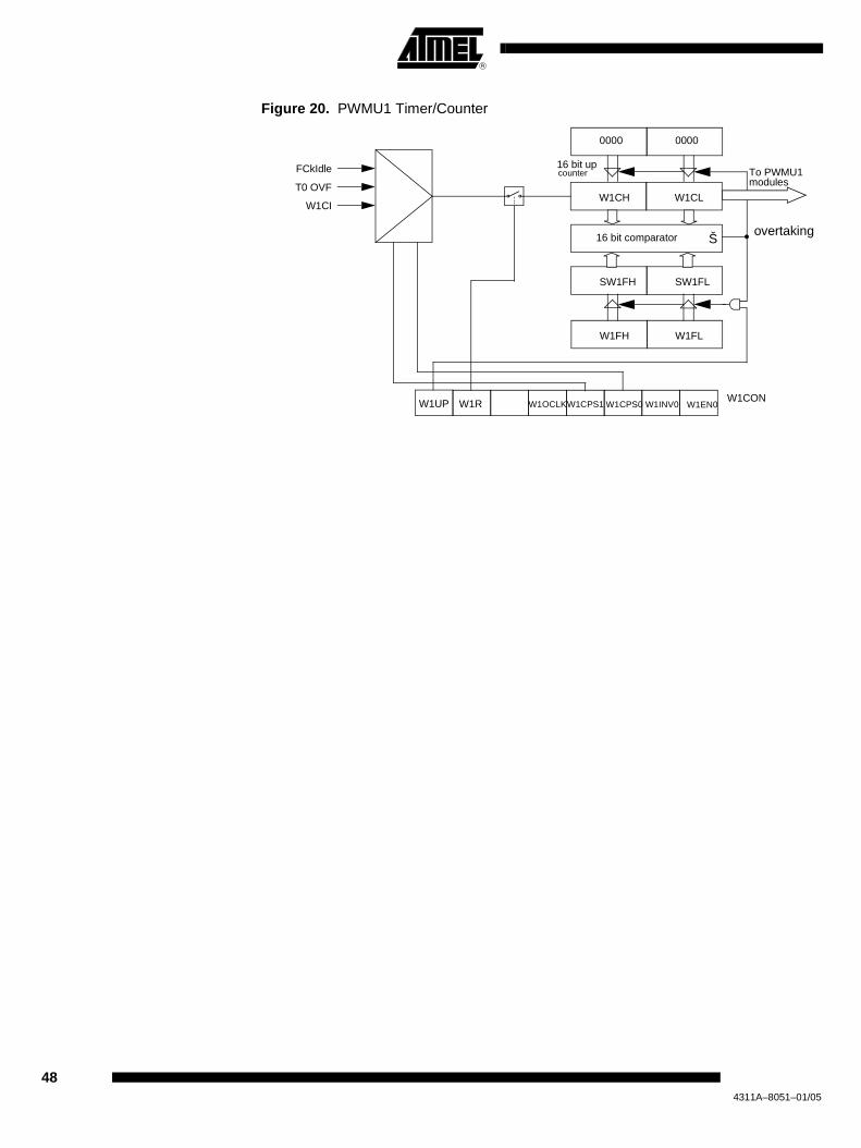
Figure 20. PWMU1 Timer/Counter
W1CPS0 W1INV0W1R W1CONW1OCLKW1CPS1W1UP W1EN0
W1CH W1CL
To PWMU1modules
FCkIdle
T0 OVF
W1CI
SW1FH SW1FL
16 bit up
W1FH W1FL
0000 0000
16 bit comparator Š
counter
overtaking
484311A–8051–01/05

Table 34. W1CON: PWMU1 Control RegisterW1CON - PWMU1 Control Register (F8h)
Reset Value = 000’RST_OCLK’ 000’RST_OCLK’bBit addressable
Table 35. W1FH: PWMU1 frequency high control registerW1FH - PWMU1 Frequency Control Register (FAh)
Reset Value = 1111 1111bNot bit addressable
7 6 5 4 3 2 1 0
W1UP W1R - W1OCLK W1CPS1 W1CPS0 W1INV0 W1EN0
Bit
Number
Bit
Mnemonic Description
7 W1UP
PWMU1 update bit
Set by software to request the load of all shadow registers on the next overtaking of the W1C counter. Reset by hardware after the loading of the shadow registers
6 W1RPWMU1 Run control bit
Set by software to turn the PWMU1 counter on. Must be cleared by software to turn the PWMU1 counter off.
5 - Not used
4 W1OCLK
Output Clocking Control bit.
This bit allows to choose between the output clocking signal and the PWM1M0 output.
If set, the external clocking is chosen, if clear, PWM1M0 is chosen.
3 W1CPS1 PWMU1 Count Pulse Select bit1
2 W1CPS0
PWMU Count Pulse Select bit0
CPS1 CPS0 Selected PWMU1 input
00 Internal clock fCkIdle
01 Reserved
10 Timer 1 Overflow
11 External clock input on W1CI at max rate = fCkIdle/4
1 W1INV0PWMU1 Module 0 inverter bit
Select the output PWM mode. If set, PWM module 0 output starts with high level.
0 W1EN0PWMU1 Module 0 enable bit
Enable PWMU1 module 0 if set. If clear, P3.5 is an I/O port.
7 6 5 4 3 2 1 0
W1F15 W1F14 W1F13 W1F12 W1F11 W1F10 W1F9 W1F8
Bit
Number
Bit
Mnemonic Description
7-0 W1F15-8PWMU1 high bits counter control frequency
The PWMU1 counter is counting from zero up to W1F15-0 value.
494311A–8051–01/05

Table 36. W1FL: PWMU1 frequency low control registerW1FL - PWMU1 Frequency Control Register (FBh)
Reset Value = 1111 1111bNot bit addressable
Table 37. W1CH: PWMU1 counter high control registerW1CH - PWMU1 Counter Control Register (FCh)
Reset Value = 0000 0000bNot bit addressable
Table 38. W1CL: PWMU1 counter low control registerW1CL - PWMU1 Counter Control Register (FDh)
Reset Value = 0000 0000bNot bit addressable
PWMU1 Output Generation
All the PWMU1 modules have the same frequency determined by the W1F registers.However, each module has is own duty cycle determined by the W1Rn Registers. (n isthe module number).
When the W1C content is lower than the value programmed via W1Rn registers, theoutput is the W1INVn-bit (low if 0, high if 1). When it is equal or higher, the output is theopposite of this W1INVn-bit (high if 0, low if 1).
When the W1C content is higher than SW1F’s, an overtaking occurs. The counter value(W1C registers) is automatically reloaded with zero (see Figure 21.). If the W1UP bit ishigh, the new comparison value is reloaded on the shadow SW1R0 registers with the
7 6 5 4 3 2 1 0
W1F7 W1F6 W1F5 W1F4 W1F3 W1F2 W1F1 W1F0
Bit
Number
Bit
Mnemonic Description
7-0 W1F7-0PWMU1 low bits counter control frequency
The PWMU1 counter is counting from zero up to W1F15-0 value.
7 6 5 4 3 2 1 0
W1C15 W1C14 W1C13 W1C12 W1C11 W1C10 W1C9 W1C8
Bit
Number
Bit
Mnemonic Description
7-0 W1C15-8 PWMU1 high bits counter frequency
7 6 5 4 3 2 1 0
W1C7 W1C6 W1C5 W1C4 W1C3 W1C2 W1C1 W1C0
Bit
Number
Bit
Mnemonic Description
7-0 W1F7-0 PWMU1 low bits counter frequency
504311A–8051–01/05

content of the W1R0 registers (see Figure 21.). This method allows to change frequencyand duty cycle without glitch.Note: If the PWMU1 is Off (W1R bit in W0CON not set), W1RnH and W1RnL contents are
automatically copied on the shadow registers SW1RnH and SW1RnLn and the contentsof W1FH and W1FL are automatically copied on the shadow registers SW1FH andSW1FL. This allows to charge the correct comparison values for each PWM module assoon as the PWMU1 timer/counter is turned on.
Figure 21. PWMU1 Interrupt System
The W1INV0 bit that allows output inversion is on the W1CON (W1 Control) register(See Table 34.).
Table 39. W1R0H: PWMU1 module 0 High Toggle RegisterW1R0H - PWMU1 Module 0 High Toggle Register (C9h)
Reset Value = 0000 0000bNot bit addressable
Table 40. W1R0L: PWMU1 module 0 Low Toggle RegisterW1R0L - PWMU1 Module 0 Low Toggle Register (CAh)
Reset Value = 0000 0000bNot bit addressable
7 6 5 4 3 2 1 0
W1R0H15 W1R0H14 W1R0H13 W1R0H12 W1R0H11 W1R0H10 W1R0H9 W1R0H8
Bit
Number
Bit
Mnemonic Description
7-0W1R0H
15-8PWMU1 Module 0 high toggle register
When the counter exceeds this value, module 0 output toggles.
7 6 5 4 3 2 1 0
W1R0L7 W1R0L6 W1R0L5 W1R0L4 W1R0L3 W1R0L2 W1R0L1 W1R0L0
Bit
Number
Bit
Mnemonic Description
7-0 W1R0L7-0PWMU1 Module 0 low toggle register
When the counter exceeds this value, module 0 output toggles.
W1CH W1CL
SW1R0H SW1R0L
W1R0H W1R0L
16 bits-comparator Š<
overtaking
Module 0 output
W1INV0W1UP
514311A–8051–01/05

PWMU1 Output Selector As shown on Figure 22., the PWMU1 can configure P3.5 to be used as
• The PWMU1 module 0 output (W1R = 1 and W1EN0 = 1)
• The External Clocking output (W1OCLK = 1 and W1EN0 = 1)
• An I/O port (W1EN0 = 0)
This configuration is made via W1CON register (See Table 34.). By default, W1CONregister contains 00h. So P3.5 is configured as an I/O port.
The W1INV0 bit allows to start PWMU1 module 0 period with a high (if set) or low level.
Figure 22. PWMU1 Output Selector
PWMU1 Interrupt System PWMU1 can generate an interrupt. The W1IC register enables or disables interrupt andinterrupt flags (See Table 41).
Figure 23. PWMU1 Interrupt Configuration
module 0 output
OCLK
W1CPS01W1INV0W1R W1CONW1ECLKW1UP W1CPS1 W1EN0
W1M0
“1”
- W1 - W1 IE0.5 IE0.7
To Interruptpriority decoder
EW1 EACF0 ECF0-W1
COF
Module 0
Overtaking
W1 -ECOF
W1IC
524311A–8051–01/05

Table 41. PWMU1 Interrupt Control RegisterW1IC - PWMU1 Interrupt Control Register (FEh)
Reset Value = 0000 0000bNot bit addressable
7 6 5 4 3 2 1 0
W1CF - - W1CF0 W1ECF - - W1ECF0
Bit
Number
Bit
Mnemonic Description
7 W1COF
PWMU1 Counter Overtaking Flag
Set by hardware when the counter rolls over. CF flags an interrupt if bit W1ECOF is set. W1COF
can be set either by hardware or software but can only be cleared by software.
6-5 - Not used
4 W1CF0PWMU1 Module 0 Toggle fla
Set by hardware when a match occurs. Can also be set by software. Must be cleared by software.
3 W1ECOFPWMU1 Counter Overtaking Flag
Set to Enable PWMU1 Counter Overtaking Flag.
2-1 - Not used
0 W1ECF0PWMU1 Module 0 Counter flag
Set to enable PWMU1 Module 0Toggle flag.
534311A–8051–01/05

WatchDog Timer AT8xEB5114 contains a powerful programmable hardware WatchDog Timer (WDT) thatautomatically resets the chip if its software fails to reset the WDT before the selectedtime interval has elapsed. It permits large Time-Out ranking from 16 ms to 2s @Fosc =12 MHz.
This WDT consists of a 14-bit counter plus a 7-bit programmable counter, a WatchDogTimer reset register (WDTRST) and a WatchDog Timer programmation (WDTPRG) reg-ister. When exiting reset, the WDT is -by default- disabled. To enable the WDT, the userhas to write the sequence 1EH and E1H into WDRST register. When the WatchDogTimer is enabled, it will increment every machine cycle while the oscillator is runningand there is no way to disable the WDT except through reset (either hardware reset orWDT overflow reset). When WDT overflows, it will generate an output RESET pulse atthe RST pin. The RESET pulse duration is 96xTOSC, where TOSC=1/FOSC. To make thebest use of the WDT, it should be serviced in those sections of code that will periodicallybe executed within the time required to prevent a WDT reset.
The WDT is controlled by two registers (WDTRST and WDTPRG)
Figure 24. WatchDog Timer
RESET Decoder
Control
WDTRST
WR
Enable
14-bit COUNTER 7-bit COUNTER
Outputs
F CPU_PERIPH
RESET
- - - - - 2 1 0
WDTPRG
544311A–8051–01/05

Figure 25. WDTPRG RegisterWDTPRG - WatchDog Timer Duration Programming register (A7h).
Reset Value = XXXX X000b
The three lower bits (S0, S1, S2) located into WDTPRG register permit to program theWDT duration.
To compute WD Time-Out, the following formula is applied:
Note: Note: Value represents the decimal value of (S2 S1 S0) / CKRL represents the Prescaler
Bit
Number
Bit
Mnemonic Description
7 -ReservedThe value read from this bit is indeterminate. Do not set this bit.
6 -ReservedThe value read from this bit is indeterminate. Do not set this bit.
5 -ReservedThe value read from this bit is indeterminate. Do not set this bit.
4 -ReservedThe value read from this bit is indeterminate. Do not set this bit.
3 -ReservedThe value read from this bit is indeterminate. Do not set this bit.
2 S2WatchDog Timer Duration selection bit 2Work in conjunction with bit 1 and bit 0.
1 S1WatchDog Timer Duration selection bit 1Work in conjunction with bit 2 and bit 0.
0 S0WatchDog Timer Duration selection bit 0Work in conjunction with bit 1 and bit 2.
S2 S1 S0 Machine Cycle Count
0 0 0 214 - 1
0 0 1 215 - 1
0 1 0 216 - 1
0 1 1 217 - 1
1 0 0 218 - 1
1 0 1 219 - 1
1 1 0 220 - 1
1 1 1 221 - 1
TimeOut FclkPeriph( )x2( )x2
12 214
2Svalue×( ) 1–( ) 15 CKRL–( )××
---------------------------------------------------------------------------------------------------------=
554311A–8051–01/05
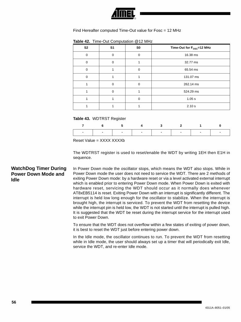
Find Hereafter computed Time-Out value for Fosc = 12 MHz
Reset Value = XXXX XXXXb
The WDTRST register is used to reset/enable the WDT by writing 1EH then E1H insequence.
WatchDog Timer During Power Down Mode and Idle
In Power Down mode the oscillator stops, which means the WDT also stops. While inPower Down mode the user does not need to service the WDT. There are 2 methods ofexiting Power Down mode: by a hardware reset or via a level activated external interruptwhich is enabled prior to entering Power Down mode. When Power Down is exited withhardware reset, servicing the WDT should occur as it normally does wheneverAT8xEB5114 is reset. Exiting Power Down with an interrupt is significantly different. Theinterrupt is held low long enough for the oscillator to stabilize. When the interrupt isbrought high, the interrupt is serviced. To prevent the WDT from resetting the devicewhile the interrupt pin is held low, the WDT is not started until the interrupt is pulled high.It is suggested that the WDT be reset during the interrupt service for the interrupt usedto exit Power Down.
To ensure that the WDT does not overflow within a few states of exiting of power down,it is best to reset the WDT just before entering power down.
In the Idle mode, the oscillator continues to run. To prevent the WDT from resettingwhile in Idle mode, the user should always set up a timer that will periodically exit Idle,service the WDT, and re-enter Idle mode.
Table 42. Time-Out Computation @12 MHz
S2 S1 S0 Time-Out for FOSC=12 MHz
0 0 0 16.38 ms
0 0 1 32.77 ms
0 1 0 65.54 ms
0 1 1 131.07 ms
1 0 0 262.14 ms
1 0 1 524.29 ms
1 1 0 1.05 s
1 1 1 2.10 s
Table 43. WDTRST Register
7 6 5 4 3 2 1 0
- - - - - - - -
564311A–8051–01/05

Analog-to-Digital Converter (ADC)
This section describes the on-chip 10 bit analog-to-digital converter of the AT8xEB5114.Six ADC channels are available for sampling of the external sources AIN0 to AIN5. Ananalog multiplexer allows the single ADC converter to select one from the 6 ADC chan-nels as ADC input voltage (ADCIN). ADCIN is converted by the 10 bit-cascadedpotentiometric ADC.
8 to 10 bits resolution can only be reached while using an external voltage reference.
For the precision conversion, set bits PSIDLE and ADSST in ADCON register to startthe conversion. The chip is in a pseudo-idle mode, the CPU doesn’t run but the periph-erals are always running. This mode allows digital noise to be lower, to ensure preciseconversion.
For accurate conversion, set bits QUIETM and ADSST in ADCON register to start theconversion. The chip is in a quiet mode, the AD is the only peripheral running. Thismode allows digital noise to be as low as possible, to ensure high precision conversion.
For these modes it is necessary to work with end of conversion interrupt, which is theonly way to wake up the chip.
If another interrupt occurs during the precision conversion, it will be treated only afterthis conversion is ended.
Features • 6 channels with multiplexed inputs
• One channel with input signal average extraction and programmable gain amplification.
• 10-bit cascaded potentiometric ADC
• Typical conversion time 20 micro-seconds
• Zero Error (offset) +/- 2 LSB max
• External Positive Reference Voltage Range 2.4 to Vcc
• Internal Positive Reference typical Voltage 2.4 Volt (1)
• ADCIN Range 0 to VREF
• Integral non-linearity typical 1 LSB (1)
• Differential non-linearity typical 0.5 LSB (1)
• Conversion Complete Flag or Conversion Complete Interrupt
• Selected ADC Clock
Note: (1): See “DC Parameters for A/D Converter” on page 88.
574311A–8051–01/05

ADC I/O Functions AINx are general I/O that are shared with the ADC channels. The channel select bit inADCF register define which ADC channel pin will be used as ADCIN. The remainingADC channels pins can be used as general purpose I/O or as the alternate function thatis available. Writings to the port registers which aren’t selected by the ADCF will nothave any effect.
Figure 26. ADC Description
Figure 27 shows the timing diagram of a complete conversion. For simplicity, the figuredepicts the waveforms in idealized form and do not provide precise timing information.For ADC characteristics and timing parameters refer to theSection “DC Parameters forA/D Converter”, page 88.
Figure 27. Timing Diagram
Note: Tsetup = 0 CLK
AIN0/P4.0
AIN1/P4.1
AIN2/P4.2
AIN3/P4.3
000
001
010
011
SCH2ADCON.2
SCH0ADCON.0
SCH1ADCON.1
CONV_CK
ADENADCON.5
ADSSTADCON.3
ADEOCADCON.4 ADC
InterruptRequest
EADCIE1.1
CONTROL
AVSS
Sample and Hold
ADDH
Vref
R/2R DAC
8
10
+
-ADDL2SAR
ADCIN
VAGND SELREFADCLK.7
2.4VADEN
ADCON.5
* gain
AIN4/P3.3
AIN5/P3.4
100
101
AC3EADCA.2
R
ADEN
ADSST
ADEOC
TSETUP
TCONV
CONV_CK
584311A–8051–01/05

Channel 3 Amplifier and Rectifying Function
If needed, the average value of the rectified signal on channel 3 can be extracted andamplified before A/D conversion as shown on Figure 28.
Figure 28. Channel 3 Amplifier
The main characteristics of this block are the following:
• Input signal level: sine wave centered around Vssa, peak value from 70 to 550 mV depending on gain, Frequency range from 35 to 70KHz. Be sure that the peak value on the amplifier output is lower than voltage supply.
• Gain: x5, x10, x15 and x20, selected using AC3E, AC3G1 and AC3G0 in ADC Amplifier register (See Table 44 and Table 52)
• Max time constant of the average value extraction: 0.5ms. When the gain is changed or when the signal levels changes from the minimum to the maximum value, a new measurement can be done after 10 time constant.
• The amplifier needs 20us to fully load the ADC hold capacitance so the ADC conversion must occurs at least 20us after the amplified channel is sampled.
• Accuracy on amplification and extraction: +/- 5% Note: The AIN3 direct channel is not equivalent to the other channels. There is a serial resis-
tance of around 100KΩ between the pin and the ADC input. So when the amplifier isbypassed, it is necessary to switch at least 20us the mux on AIN3 input before starting aconversion.
Table 44. ADCF Register
ADCA (S:F7h)ADC Amplifier Configuration
Reset Value = 0000 0000b
AIN3/P4.3A/D input
Amplification
(programmable gain)
AC3G1ADCF.7
AC3EADCF.5
AC3G0ADCF.6
EnableGain
Average valueextraction
7 6 5 4 3 2 1 0
- - - - - AC3E AC3G1 AC3G0
Bit Number
Bit Mnemonic Description
7-3 - Not used
2 AC3EEnable Channel 3 amplifierSet to enable amplifier.Clear for Standby mode
1 AC3G1 Channel 3 amplifier gain
AC3G1 AC3G0
0 0 gain x5
0 1 gain x10
1 0 gain x15
1 1 gain x20
0 AC3G0
594311A–8051–01/05
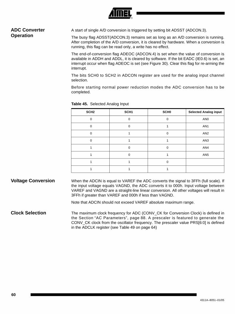
ADC Converter Operation
A start of single A/D conversion is triggered by setting bit ADSST (ADCON.3).
The busy flag ADSST(ADCON.3) remains set as long as an A/D conversion is running.After completion of the A/D conversion, it is cleared by hardware. When a conversion isrunning, this flag can be read only, a write has no effect.
The end-of-conversion flag ADEOC (ADCON.4) is set when the value of conversion isavailable in ADDH and ADDL, it is cleared by software. If the bit EADC (IE0.6) is set, aninterrupt occur when flag ADEOC is set (see Figure 30). Clear this flag for re-arming theinterrupt.
The bits SCH0 to SCH2 in ADCON register are used for the analog input channelselection.
Before starting normal power reduction modes the ADC conversion has to becompleted.
Table 45. Selected Analog Input
Voltage Conversion When the ADCIN is equal to VAREF the ADC converts the signal to 3FFh (full scale). Ifthe input voltage equals VAGND, the ADC converts it to 000h. Input voltage betweenVAREF and VAGND are a straight-line linear conversion. All other voltages will result in3FFh if greater than VAREF and 000h if less than VAGND.
Note that ADCIN should not exceed VAREF absolute maximum range.
Clock Selection The maximum clock frequency for ADC (CONV_CK for Conversion Clock) is defined inthe Section “AC Parameters”, page 88. A prescaler is featured to generate theCONV_CK clock from the oscillator frequency. The prescaler value PRS[6:0] is definedin the ADCLK register (see Table 49 on page 64)
SCH2 SCH1 SCH0 Selected Analog input
0 0 0 AN0
0 0 1 AN1
0 1 0 AN2
0 1 1 AN3
1 0 0 AN4
1 0 1 AN5
1 1 0
1 1 1
604311A–8051–01/05
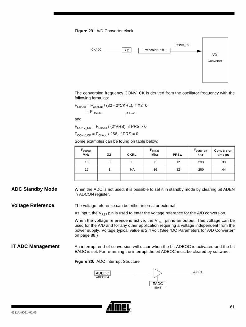
Figure 29. A/D Converter clock
The conversion frequency CONV_CK is derived from the oscillator frequency with thefollowing formulas:
FCkAdc = FOscOut / (32 - 2*CKRL), if X2=0
= FOscOut , if X2=1
and
FCONV_CK = FCkAdc / (2*PRS), if PRS > 0
FCONV_CK = FCkAdc / 256, if PRS = 0
Some examples can be found on table below:
ADC Standby Mode When the ADC is not used, it is possible to set it in standby mode by clearing bit ADENin ADCON register.
Voltage Reference The voltage reference can be either internal or external.
As input, the VREF pin is used to enter the voltage reference for the A/D conversion.
When the voltage reference is active, the VREF pin is an output. This voltage can beused for the A/D and for any other application requiring a voltage independent from thepower supply. Voltage typical value is 2.4 volt (See “DC Parameters for A/D Converter”on page 88.)
IT ADC Management An interrupt end-of-conversion will occur when the bit ADEOC is activated and the bitEADC is set. For re-arming the interrupt the bit ADEOC must be cleared by software.
Figure 30. ADC Interrupt Structure
FOscOut
MHz X2 CKRL
FCkAdc
Mhz PRSw
FCONV_CK
khzConversion
time µs
16 0 F 8 12 333 33
16 1 NA 16 32 250 44
Prescaler PRS
A/D
Converter
CONV_CK
CKADC / 2
ADEOCADCON.4
EADCIE0.6
ADCI
614311A–8051–01/05
Accuracy improvement on analog to digital conversion using the internal voltage reference
Overview The internal Vref absolute accuracy is around 4%. This variation is mainly due to thetemperature, the process, and the voltage variations. In order to increase the accuracyof the measurements made thanks to the ADC, it is possible to make a software correc-tion of the Vref, in order to calculate the result the ADC should have returned in case theVref was more accurate.
The idea of this improvement is the following: Because there is an EEPROM stacked onthe product, it is possible to store a linear coefficient which allow a correction of the pro-cess variations.
Coefficient address The coefficient is stored at the address 0x00 of the serial data EEPROM stacked on theAT8xEB5114.
Coefficient format In order to ease the calculation, this coefficient has been stored as a floating decimalnumber corresponding to Table 46.
Table 46. Calibration coefficient storage format
It means that if the value is 0x80, the coefficient is equal to 1. If the coefficient is 0x7e,the coefficient is equal to 0,111 1110 in binary which is 0,983 in decimal.
During the test, the Vref is measured, and the calibration value calculated is stored atthe address 0x00 of the stack die in accordance with the Table 46 format value.
The relation between the coefficient stored, and the true Vref measurement arerecorded on the Table 47.
Table 47. Relation between True Vref measurement and coefficient stored into theEEPROM
Bit Value
7 1,
6 1/2
5 1/4
4 1/8
3 1/16
2 1/32
1 1/64
0 1/128
True Vref
Value (V)
Min 2.300 2.316 2.334 2.353 2.372 2.391 2.409 2.428 2.447 2.466 2.484
Typ 2.306 2.325 2.345 2.362 2.381 2.400 2.419 2.438 2.456 2.475 2.494
Max 2.316 2.334 2.353 2.372 2.391 2.409 2.428 2.447 2.466 2.484 2.500
Value stored 0x7b 0x7c 0x7d 0x7e 0x7f 0x80 0x81 0x82 0x83 0x84 0x85
decimal value 0.961 0.969 0.977 0.984 0.992 1 1.008 1.016 1.023 1.031 1.039
624311A–8051–01/05

How to Take Advantage of the Calibration Value
The coefficient stored on the stacked die allow to determine the conversion result theAT8xEB5114 should have returned in case its Vref was exactly equal to 2.4V. In order todetermine it, a multiplication of the result of the conversion with the coefficient stored inthe stack, followed by a shift are sufficient.
Example Vref is 2.36V instead of 2.4V, and only 8 bits are necessary.
The value measured during the test 2.36V. So, in accordance with the Table 47, thecoefficient which has to be stored on the EEPROM is 0x7e which corresponds to0.1111110 in binary, which also corresponds to around 2.36/2.4.
If, for example, after a conversion, the ADDH register contains 0xf0, to know the resultthe ADC should have returned in case the Vref was really at 2.4V, the following opera-tions are necessary:
0xf0 * 0x7e = 1111 0000 * 0111 1110 = 0x7620 = 0111 0110 0010 0000.
So because of the point on the coefficient, the result is 1110 110 which is 0xec.
Assembler code example This is an example of assembler code optimized for size and fast recalculation in case 8bits are sufficient.
start_adjustement : MOV B,coeff ; Coeff
MOV A,ADDH ; ADC result
MUL AB ;
RLC A ; Recover lowest bit
MOV A,B ;
RLC A ; Recover result
JNC end_fix ; Result OK
MOV A,#0ffh ; Overflow
end_adjustement : RET
The new result is stored on the accumulator.
This routine requires 15 bytes + 3 bytes for the long call (LCALL).
The execution of the subroutine (including the LCALL) is 18 cycles in normal case and19 cycles in case of overflow (less than 10us with a 12 MHz oscillator and the X2 mode).
Registers Table 48. ADCON Register ADCON (S:F3h)ADC Control Register
7 6 5 4 3 2 1 0
QUIETM PSIDLE ADEN ADEOC ADSST SCH2 SCH1 SCH0
Bit Number
Bit Mnemonic Description
7 QUIETMQuiet mode (best precision)Set to put in quiet mode during conversion.Cleared by hardware after completion of the conversion.
6 PSIDLEPseudo Idle mode (good precision)Set to put in idle mode during conversion.Cleared by hardware after completion of the conversion.
634311A–8051–01/05

Reset Value = X000 0000b
Table 49. ADCLK RegisterADCLK (S:F2h)ADC Clock Prescalersc
Reset Value = 0000 0000b
Table 50. ADDH RegisterADDH (S:F5h Read Only)ADC Data High byte register
Read only register
Reset Value = 00h
5 ADENEnable/Standby ModeSet to enable ADC.Clear for Standby mode.
4 ADEOC
End Of ConversionSet by hardware when ADC result is ready to be read. This flag can generate an interrupt.Must be cleared by software.
3 ADSSTStart and StatusSet to start an A/D conversion.Cleared by hardware after completion of the conversion.
2-0 SCH2:0Selection of channel to convertsee Table 45 on page 60.
7 6 5 4 3 2 1 0
SELREF PRS 6 PRS 5 PRS 4 PRS 3 PRS 2 PRS 1 PRS 0
Bit Number
Bit Mnemonic Description
7 SELREFSelection and activation of the internal 2.4V voltage referenceSet to enable the internal voltage reference.Clear to disable the internal voltage reference.
6-0 PRS6:0Clock PrescalerfCONV_CK = fCkADC / (2 * PRS)
if PRS=0, fCONV_CK = fCkADC / 256
7 6 5 4 3 2 1 0
ADAT 9 ADAT 8 ADAT 7 ADAT 6 ADAT 5 ADAT 4 ADAT 3 ADAT 2
Bit Number
Bit Mnemonic Description
7-0 ADAT9:2ADC resultbits 9-2
Bit Number
Bit Mnemonic Description
644311A–8051–01/05

Table 51. ADDL RegisterADDL (S:F4h Read Only)ADC Data Low byte register
Read only register
Reset Value = xxxx xx00b
7 6 5 4 3 2 1 0
- - - - - - ADAT 1 ADAT 0
Bit Number
Bit Mnemonic Description
7-6 -ReservedThe value read from these bits are indeterminate. Do not set these bits.
1-0 ADAT1:0ADC resultbits 1-0
654311A–8051–01/05
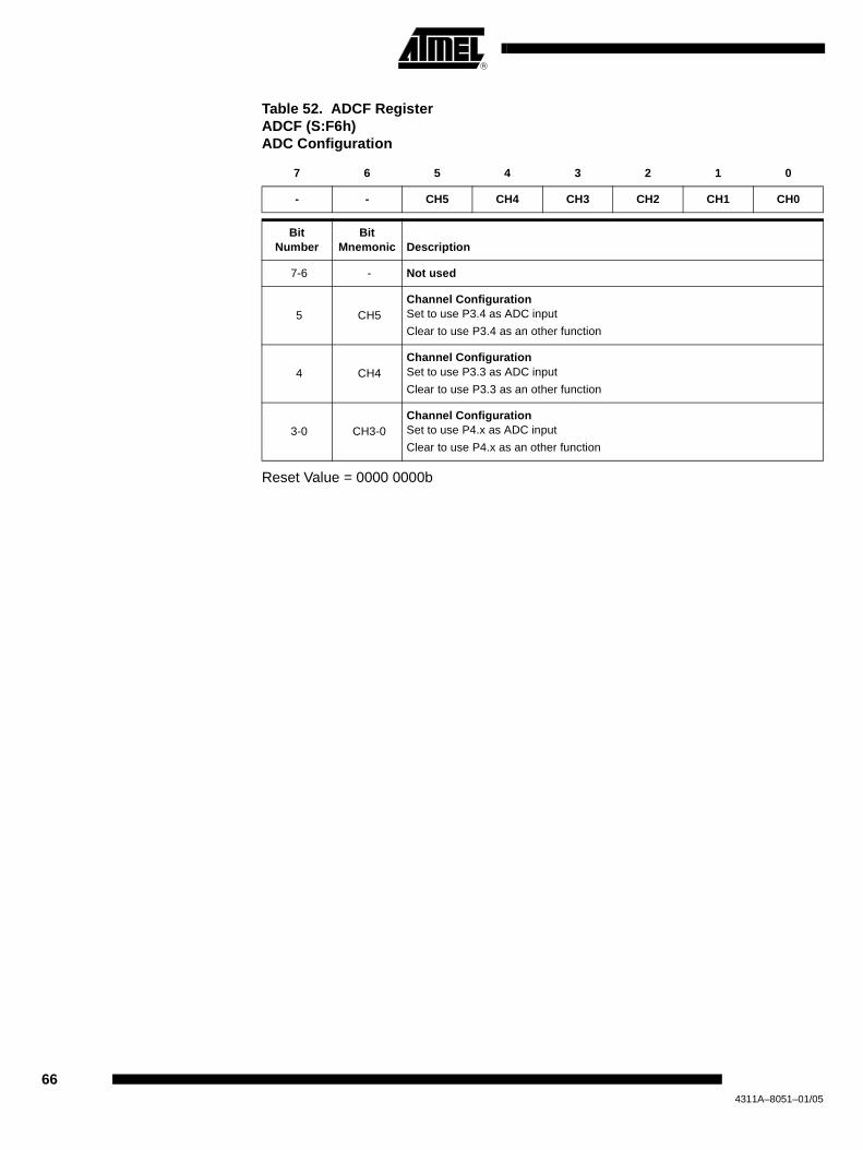
Table 52. ADCF RegisterADCF (S:F6h)ADC Configuration
Reset Value = 0000 0000b
7 6 5 4 3 2 1 0
- - CH5 CH4 CH3 CH2 CH1 CH0
Bit Number
Bit Mnemonic Description
7-6 - Not used
5 CH5Channel Configuration Set to use P3.4 as ADC input
Clear to use P3.4 as an other function
4 CH4Channel Configuration Set to use P3.3 as ADC input
Clear to use P3.3 as an other function
3-0 CH3-0Channel Configuration Set to use P4.x as ADC input
Clear to use P4.x as an other function
664311A–8051–01/05
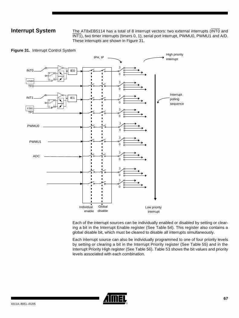
Interrupt System The AT8xEB5114 has a total of 8 interrupt vectors: two external interrupts (INT0 andINT1), two timer interrupts (timers 0, 1), serial port interrupt, PWMU0, PWMU1 and A/D.These interrupts are shown in Figure 31.
Figure 31. Interrupt Control System
Each of the interrupt sources can be individually enabled or disabled by setting or clear-ing a bit in the Interrupt Enable register (See Table 54). This register also contains aglobal disable bit, which must be cleared to disable all interrupts simultaneously.
Each interrupt source can also be individually programmed to one of four priority levelsby setting or clearing a bit in the Interrupt Priority register (See Table 55) and in theInterrupt Priority High register (See Table 56). Table 53 shows the bit values and prioritylevels associated with each combination.
0
3
High priority
interrupt
Interruptpollingsequence
Low priorityinterrupt
Globaldisable
Individualenable
TF0
INT0
TF1
IPH, IP
IE0
0
3
0
3
0
3
0
3
0
3
0
3
ADC
0
3
0
3PWMU0
PWMU1
0
1ESB0
INT1 IE10
1ESB1
674311A–8051–01/05

Table 53. Priority Bit Level Values
A low-priority interrupt can be interrupted by a high priority interrupt, but not by anotherlow-priority interrupt. A high-priority interrupt can’t be interrupted by any other interruptsource.
If two interrupt requests of different priority levels are received simultaneously, therequest of higher priority level is serviced. If interrupt requests of the same priority levelare received simultaneously, an internal polling sequence determines which request isserviced. Thus within each priority level there is a second priority structure determinedby the polling sequence.
IPH.x IP.x Interrupt Level Priority
0 0 0 (Lowest)
0 1 1
1 0 2
1 1 3 (Highest)
Interrupt Name Interrupt Address Vector Priority Number
external interrupt (INT0) 0003h 1
Timer0 (TF0) 000Bh 2
external interrupt (INT1) 0013h 3
Timer1 (TF1) 001Bh 4
PWM0 0023h 5
PWM1 002Bh 6
ADC 0033h 7
684311A–8051–01/05

Reset Value = 0000 0000bBit addressable
Table 54. IEN0 RegisterIEN0 - Interrupt Enable Register (A8h)
7 6 5 4 3 2 1 0
EA EADC EW1 EW0 ET1 EX1 ET0 EX0
Bit Number
Bit Mnemonic Description
7 EA
Enable All interrupt bitClear to disable all interrupts.Set to enable all interrupts.If EA=1, each interrupt source is individually enabled or disabled
by setting or clearing its interrupt enable bit.
6 EADCADC Interrupt Enable
Clear to disable the ADC interrupt.Set to enable the ADC interrupt.
5 EW1PWM1 Enable bit
Clear to disable PWMU interrupt.Set to enable PWMU port interrupt.
4 EW0PWM0 Enable bit
Clear to disable PWMU interrupt.Set to enable PWMU port interrupt.
3 ET1Timer 1 overflow interrupt Enable bit
Clear to disable timer 1 overflow interrupt.Set to enable timer 1 overflow interrupt.
2 EX1External interrupt 1 Enable bit
Clear to disable external interrupt 1.Set to enable external interrupt 1.
1 ET0Timer 0 overflow interrupt Enable bit
Clear to disable timer 0 overflow interrupt.Set to enable timer 0 overflow interrupt.
0 EX0External interrupt 0 Enable bit
Clear to disable external interrupt 0.Set to enable external interrupt 0.
694311A–8051–01/05

Reset Value = X000 0000bBit addressable.
Table 55. IPL0 RegisterIPL0 - Interrupt Priority Register (B8h)
7 6 5 4 3 2 1 0
- PADC PW1 PW0 PT1 PX1 PT0 PX0
Bit Number
Bit Mnemonic Description
7 -Reserved
The value read from this bit is indeterminate. Do not set this bit.
6 PADCADC interrupt Priority bit
Refer to PADCH for priority level
5 PW1PWMU1 Priority bit
Refer to PW1H for priority level.
4 PW1PWMU0 Priority bit
Refer to PW1H for priority level.
3 PT1Timer 1 overflow interrupt Priority bit
Refer to PT1H for priority level.
2 PX1External interrupt 1 Priority bit
Refer to PX1H for priority level.
1 PT0Timer 0 overflow interrupt Priority bit
Refer to PT0H for priority level.
0 PX0External interrupt 0 Priority bit
Refer to PX0H for priority level.
704311A–8051–01/05

Reset Value = X000 0000bNot bit addressable
Table 56. IPH0 RegisterIPH0 - Interrupt Priority High Register (B7h)
7 6 5 4 3 2 1 0
- PADCH PW1H PW0H PT1H PX1H PT0H PX0H
Bit Number
Bit Mnemonic Description
7 -Reserved
The value read from this bit is indeterminate. Do not set this bit.
6 PADCH
ADC Interrupt Priority level most significant bitPADCH PADC Priority level0 0 Lowest0 11 01 1 Highest
5 PW1H
PWMU1 Priority High bitPW1H PW1 Priority Level0 0 Lowest0 11 01 1 Highest
4 PW1H
PWMU0 Priority High bitPW1H PW1 Priority Level0 0 Lowest0 11 01 1 Highest
3 PT1H
Timer 1 overflow interrupt Priority High bitPT1H PT1 Priority Level0 0 Lowest0 11 01 1 Highest
2 PX1H
External interrupt 1 Priority High bitPX1H PX1 Priority Level0 0 Lowest0 11 01 1 Highest
1 PT0H
Timer 0 overflow interrupt Priority High bitPT0H PT0 Priority Level0 0 Lowest0 11 01 1 Highest
0 PX0H
External interrupt 0 Priority High bitPX0H PX0 Priority Level0 0 Lowest0 11 01 1 Highest
714311A–8051–01/05

Flash Memory As shown Figure 32, the Flash version of AT8xEB5114 implements 4 Kbytes of on-chipprogram/code memory.
The Flash memory increases EPROM and ROM functionality by in-circuit electrical era-sure and programming. Thanks to the internal charge pump, the high voltage needed forprogramming or erasing Flash cells is generated on-chip using the standard VDDvoltage.
Hardware programming mode is available using specific programming tool.
AT8xEB5114 features a Flash memory containing 4 Kbytes of program memory (userspace) organized into 128 byte pages,
This Flash memory is programmable by parallel programming.
Figure 32. Flash Memory Architecture
FM0 Memory Architecture
The Flash memory is made up of 4 blocks (see Figure 32):
– The memory array (user space) 4 Kbytes
– The Extra Row
– The Hardware security bits
– The column latch registers
User Space This space is composed of a 4 Kbytes Flash memory organized in 32 pages of 128bytes. It contains the user’s application code.
Extra Row (XRow) This row is a part of flash memory and has a size of 128 bytes. The extra row may con-tain information for boot loader usage.
Hardware security Byte The Hardware Security Byte space is a part of flash memory and has a size of 1 byte.The 4 MSB can be read/written by software, the 4 LSB can only be read by software andwritten by hardware in parallel mode.
Column latches The column latches, also part of flash memory, have a size of full page (128 bytes).The column latches are the entrance buffers of the three previous memory locations(user array, XROW and Hardware security byte).
Overview of Flash Memory Operations
The CPU interfaces to the Flash memory through the FCON register used to:
– Map the memory spaces in the adressable space
0FFFh
4 Kbytes
Flash memory
0000h
Hardware Security (1 byte)
Column Latches (128 bytes)
user space
Extra Row (128 bytes)
724311A–8051–01/05
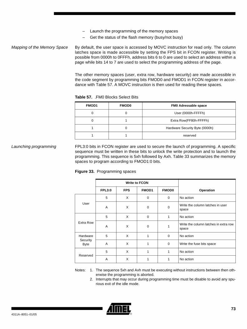
– Launch the programming of the memory spaces
– Get the status of the flash memory (busy/not busy)
Mapping of the Memory Space By default, the user space is accessed by MOVC instruction for read only. The columnlatches space is made accessible by setting the FPS bit in FCON register. Writing ispossible from 0000h to 0FFFh, address bits 6 to 0 are used to select an address within apage while bits 14 to 7 are used to select the programming address of the page.
The other memory spaces (user, extra row, hardware security) are made accessible inthe code segment by programming bits FMOD0 and FMOD1 in FCON register in accor-dance with Table 57. A MOVC instruction is then used for reading these spaces.
Table 57. .FM0 Blocks Select Bits
Launching programming FPL3:0 bits in FCON register are used to secure the launch of programming. A specificsequence must be written in these bits to unlock the write protection and to launch theprogramming. This sequence is 5xh followed by Axh. Table 33 summarizes the memoryspaces to program according to FMOD1:0 bits.
Figure 33. Programming spaces
Notes: 1. The sequence 5xh and Axh must be executing without instructions between then oth-erwise the programming is aborted.
2. Interrupts that may occur during programming time must be disable to avoid any spu-rious exit of the idle mode.
FMOD1 FMOD0 FM0 Adressable space
0 0 User (0000h-FFFFh)
0 1 Extra Row(FF80h-FFFFh)
1 0 Hardware Security Byte (0000h)
1 1 reserved
Write to FCON
OperationFPL3:0 FPS FMOD1 FMOD0
User
5 X 0 0 No action
A X 0 0Write the column latches in user space
Extra Row
5 X 0 1 No action
A X 0 1Write the column latches in extra row space
Hardware Security
Byte
5 X 1 0 No action
A X 1 0 Write the fuse bits space
Reserved5 X 1 1 No action
A X 1 1 No action
734311A–8051–01/05

Status of the Flash Memory The bit FBUSY in FCON register is used to indicate the status of programming. FBUSYis set when programming is in progress.
Loading the Column Latches Any number of data from 1 byte to 128 bytes can be loaded in the column latches. Thisprovides the capability to program the whole memory by byte, by page or by any numberof bytes in a page.When programming is launched, an automatic erase of the locations loaded in the col-umn latches is first performed, then programming is effectively done. Thus no page orblock erase is needed and only the loaded data are programmed in the correspondingpage.
The following procedure is used to load the column latches and is summarized inFigure 34:
– Disable interrupt and map the column latch space by setting FPS bit.
– Load the DPTR with the address to load.
– Load Accumulator register with the data to load.
– Execute the MOVX @DPTR, A instruction.
– If needed loop the three last instructions until the page is completely loaded.
– unmap the column latch and Enable Interrupt
Figure 34. Column Latches Loading Procedure
Note: The last page address used when loading the column latch is the one used to select thepage programming address.
Column Latches Loading
Data LoadDPTR= Address
ACC= DataExec: MOVX @DPTR, A
Last Byteto load?
Column Latches MappingFPS= 1
Data memory MappingFPS= 0
Disable ITEA= 0
Enable ITEA= 1
744311A–8051–01/05

Programming the Flash Spaces User
The following procedure is used to program the User space and is summarized inFigure 35:
– Load data in the column latches from address 0000h to 0FFFh1.
– Disable the interrupts.
– Launch the programming by writing the data sequence 50h followed by A0hin FCON register (only from FM1).The end of the programming indicated by the FBUSY flag cleared.
– Enable the interrupts.Note: 1. The last page address used when loading the column latch is the one used to select
the page programming address.
Extra Row
The following procedure is used to program the Extra Row space and is summarized inFigure 35:
– Load data in the column latches from address FF80h to FFFFh.
– Disable the interrupts.
– Launch the programming by writing the data sequence 52h followed by A2hin FCON register (only from FM1).The end of the programming indicated by the FBUSY flag cleared.
– Enable the interrupts.
754311A–8051–01/05

Figure 35. Flash and Extra row Programming Procedure
Hardware Security Byte
The following procedure is used to program the Hardware Security Byte spaceand is summarized in Figure 36:
– Set FPS and map Hardware byte (FCON = 0x0C)
– Disable the interrupts.
– Load DPTR at address 0000h.
– Load Accumulator register with the data to load.
– Execute the MOVX @DPTR, A instruction.
– Launch the programming by writing the data sequence 54h followed by A4hin FCON register (only from FM1).The end of the programming indicated by the FBusy flag cleared.
– Enable the interrupts.
Flash Spaces Programming
Disable ITEA= 0
Launch ProgrammingFCON= 5xhFCON= Axh
End ProgrammingEnable IT
EA= 1
Column Latches Loadingsee Figure 34
• FBusyCleared?
Erase ModeFCON = 00h
764311A–8051–01/05

Figure 36. Hardware Programming Procedure
Reading the Flash Spaces User
The following procedure is used to read the User space and is summarized in Figure 37:
– Map the User space by writing 00h in FCON register.
– Read one byte in Accumulator by executing MOVC A,@A+DPTR with A= 0& DPTR= 0000h to FFFFh.
Extra Row
The following procedure is used to read the Extra Row space and is summarized inFigure 37:
– Map the Extra Row space by writing 02h in FCON register.
– Read one byte in Accumulator by executing MOVC A,@A+DPTR with A= 0& DPTR= FF80h to FFFFh.
– Clear FCON to unmap the Extra Row.
Hardware Security Byte
Flash Spaces Programming
Disable ITEA= 0
Launch ProgrammingFCON= 54hFCON= A4h
End ProgrammingEnable IT
EA= 1
FBusyCleared?
Erase ModeFCON = 00h
Data LoadDPTR= 00hACC= Data
Exec: MOVX @DPTR, A
FCON = 0Ch
774311A–8051–01/05

The following procedure is used to read the Hardware Security space and issummarized in Figure 37:
– Map the Hardware Security space by writing 04h in FCON register.
– Read the byte in Accumulator by executing MOVC A,@A+DPTR with A= 0 &DPTR= 0000h.
– Clear FCON to unmap the Hardware Security Byte.
Figure 37. Reading Procedure
Flash Protection from Parallel Programming
The three lock bits in Hardware Security Byte are programmed according to Table 58,will provide different level of protection for the on-chip code and data located in flashmemory.
The only way for write this bits are the parallel mode.
Table 58. Program Lock Bit
WARNING: Security level 2 and 3 should only be programmed after Flash and Coreverification.
Flash Spaces Reading
Flash Spaces MappingFCON= 00000xx0b
Data ReadDPTR= Address
ACC= 0Exec: MOVC A, @A+DPTR
Erase ModeFCON = 00h
Program Lock Bits Protection Description
Security
level LB1 LB0
1 U U No program lock feature enabled.
2 U PWriting Flash data from programmer is disabled but still allowed from internal code execution.
3 P UWriting and reading Flash data from programmer is disabled but still allowed from internal code execution.
784311A–8051–01/05

RegistersTable 59. FCON: Flash Control RegisterFCON - Flash Control Register (D1h)
Reset Value= 0000 0000b
7 6 5 4 3 2 1 0
FPL3 FPL2 FPL1 FPL0 FPS FMOD1 FMOD0 FBUSY
Bit Number
Bit Mnemonic Description
7-4 FPL3:0Programming Launch Command BitsWrite 5Xh followed by AXh to launch the programming according to FMOD1:0. (see Figure 33.)
3 FPSFlash Map Program Space Set to map the column latch space in the data memory space.Clear to re-map the data memory space.
2-1 FMOD1:0 Flash ModeSee Table 57 or Table 33.
0 FBUSY
Flash BusySet by hardware when programming is in progress.Clear by hardware when programming is done.Can not be cleared by software.
794311A–8051–01/05

AT8xEB5114 ROM
ROM Structure The AT8xEB5114 ROM memory is divided in two different arrays:
• the code array: 4 Kbytes.
• the configuration byte:1 byte.
Hardware Configuration Byte The configuration byte sets the starting microcontroller options and the security levels.
The starting default options are X1 mode, Oscillator A.
HSB = 1111 XX11bNote: Whatever the value of RST_OSC, the XTAL1 input is always validated in order to enter in
test modes.
Table 60. Hardware Security Byte (HSB)HSB (S:EFh)Power configuration Register
7 6 5 4 3 2 1 0
X2 RST_OSC1 RST_OSC0 RST_OCLK - - LB1 LB0
Bit
Number
Bit
Mnemonic Description
7 X2X2 ModeClear to force X2 mode (CkOut = OscOut)
Set to use the prescaler mode (CkOut = OscOut / (2*(16-M)))
6 RST_OSC1 Oscillator bit 1 on reset
5 RST_OSC0
Oscillator bit 0 on reset
Oscillator bit on reset
11: allow OSCA10: allow OSCB
01: allow OSCC
00: reserved
4 RST_OCLK
Output clocking signal after RESET
Clear to start the microcontroller with a low level on P3.5 followed by an output clocking signal on P3.5 as soon as the microcontroller is started. This signal has is a 1/3 high 2/3 low signal. Its frequency is equal to (CKout / 3).
Set to start on normal conditions: No signal on P3.5 which is pulled up.
3 CKRLRV
CKRL Reset Value
If set, the microcontroller starts with the prescaler reset value = XXXX 1000 (OscOut = CkOut/16).
If clear, the microcontroller starts with a prescaler reset value = XXXX 1111 (OscOut = CkOut/2).
2 - Reserved
1-0 LB1-0User Program Lock Bits
See Table 61 on page 81
804311A–8051–01/05

ROM Lock System The program Lock system, when programmed, protects the on-chip program againstsoftware piracy.
Program ROM lock Bits The lock bits when programmed according to Table 61 will provide different level of pro-tection for the on-chip code and data.
U: unprogrammedP: programmed
Table 61. Program Lock bits
Program Lock Bits Protection Description
Security
level LB1 LB0
1 U U No program lock feature enabled.
3 P U Reading ROM data from programmer is disabled.
814311A–8051–01/05

824311A–8051–01/05
834311A–8051–01/05
Stacked EEPROM
Overview The AT8xEB5114 features a stacked 2-wire serial data EEPROM. The data EEPROMallows to save up to 256 bytes. The EEPROM is internally connected to P3.6 and P3.7which are respectively connected to the SDA and the SCL pins.
Protocol In order to access this memory, it is necessary to use software subroutines according tothe AT24C02 datasheet. Nevertheless, because the internal pull-up resistors of theAT8xEB5114 is quite high (around 100KΩ), the protocol should be slowed in order to besure that the SDA pin can rise to the high level before reading it.
Another solution to keep the access to the EEPROM in specification is to work with asoftware pull-up.
Using a software pull-up, consists of forcing a low level at the output pin of the microcon-troller before configuring it as an input (high level).
The C51 the ports are “quasi-bidirectional” ports. It means that the ports can be config-ured as output low or as input high. In case a port is configured as an output low, it cansink a current and all internal pull-ups are disconnected. In case a port is configured asan input high, it is pulled up with a strong pull-up (a few hundreds Ohms resistor) for 2clock periods. Then, if the port is externally connected to a low level, it is only kept highwith a weak pull up (around 100KΩ), and if not, the high level is latched high thanks to amedium pull (around 10kΩ).
Thus, when the port is configured as an input, and when this input has been read at alow level, there is a pull-up of around 100KΩ, which is quite high, to quickly load theSDA capacitance. So in order to help the reading of a high level just after the reading ofa low level, it is possible to force a transition of the SDA port from an input state (1), toan output low state (0), followed by a new transition from this output low state to inputstate; In this case, the high pull-up has been replaced with a low pull-up which warran-ties a good reading of the data.

Electrical Characteristics
Absolute Maximum Ratings(*)
Power Consumption Measurement
Since the introduction of the first C51 devices, every manufacturer made operating Iccmeasurements under reset, which made sense for the designs where the CPU was run-ning under reset. In our new devices, the CPU is no longer active during reset, so thepower consumption is very low and this is not really representative of what will happenin the customer’s system. Thus, while keeping measurements under Reset, we presenta new way to measure the operating Icc:
Using an internal test ROM, the following code is executed:
Label: SJMP Label (80 FE)
Ports 3, 4 are disconnected, RST = Vcc, XTAL2 is not connected and XTAL1 is drivenby the clock.
This is much more representative of the real operating Icc.
DC Parameters for Low Voltage
TA = 0°C to +70°C; VSS = 0 V; VCC = 3 V to 3.6 V; F = 0 to 24 MHz.TA = -40°C to +85°C; VSS = 0 V; VCC = 3 V to 3.6 V; F = 0 to 24 MHz.
Ambient Temperature Under Bias:C = commercial..................................................... 0°C to 70°CI = industrial ....................................................... -40°C to 85°CStorage Temperature ................................... -65°C to + 150°CVoltage on VCC to VSS.....................................-0.5 V to + 4.6 VVoltage on Any Pin to VSS .......................-0.5 V to VCC + 0.5 VPower Dissipation.............................................................. 1 WElectro-static discharge voltage 1500 V
*NOTICE: Stresses at or above those listed under “Abso-lute Maximum Ratings” may cause permanent damage to the device. This is a stress rating only and functional operation of the device at these or any other conditions above those indicated in the operational sections of this specification is not implied. Exposure to absolute maximum rating conditions may affect device reliability.Power Dissipation value is based on the maxi-mum allowable die temperature and the thermal resistance of the package.
Table 1. DC Parameters for Low Voltage
Symbol Parameter Min Typ Max Unit Test Conditions
VIL Input Low Voltage -0.5 0.8 V
VIH Input High Voltage except XTAL1, RST 2 VCC + 0.5 V
VIH1 Input High Voltage, XTAL1, RST 0.7 VCC VCC + 0.5 V
VOL Output Low Voltage, ports 3, 4(6)
0.3
0.45
1.0
V
V
V
IOL = 100 µA
IOL = 1.6 mA
IOL = 3.2 mA
VOH Output High Voltage, ports 3, 4.(6)
0.9 VCC
VCC - 0.7
VCC - 1.4
V
V
V
IOH = -10 µA
IOH =-30 µA
IOH = -50µA
844311A–8051–01/05

VOH2 Output High Voltage, ports 3, 4.(6) mode Push pull
0.9VCC
VCC - 0.7
VCC - 1.5
V
V
V
IOH = -100 µA
IOH = - 1 mA
IOH = - 2 mA
IIL Logical 0 Input Current ports 3 and 4(7) -50 µA Vin = 0.45 V
IIL Input Leakage Current ±10 µA 0.45 V < Vin < VCC
ITL Logical 1 to 0 Transition Current, ports 3, 4 (8) -650 µA Vin = 2.0 V
RRST RST Pull up Resistor 50 90 (5) 200 kΩ
CIO Capacitance of I/O Buffer 10 pFFc = 1 MHzTA = 25°C
IPD Power Down Current 50 200 µA VCC = 3.0 V to 3.6 V(3)
FOSCB OSCB unlocked frequency 10.8 12 13.2 MHz With ideal R and C
FOSCB OSCB locked frequency 11.5 12 12.5 MHz With ideal R and C
FOSC C OSCC frequency 8.4 14 19.6 MHz
ICC
under
RESET
Power Supply Current Maximum values, X1 mode, OSCA oscillator (9) 4 mA
VCC = 3.3 V(1)
OSCA + Prescaler
ICC
operatingPower Supply Current Maximum values, X1 mode, OSCA oscillator (9) 0.4*F+3 mA
VCC = 3.3 V(10)
F in MHz
ICC
idlePower Supply Current Maximum values, X1 mode, OSCA oscillator (9)
6
mA VCC = 3.3 V(2)
ICC
under
RESET
Power Supply Current Maximum values, X1 mode, OSCB oscillator (9) 900 uA
VCC = 3.3 V(1)
OSCB + Prescaler
ICC
operatingPower Supply Current Maximum values, X1 mode, OSCB oscillator (9) 5 mA VCC = 3.3 V(10)
ICC
idlePower Supply Current Maximum values, X1 mode, OSCB oscillator (9) 4.8
mA VCC = 3.3 V(2)
ICC
under
RESET
Power Supply Current Maximum values, X1 mode, OSCC oscillator (9) 650 µA
VCC = 3.3 V(1)
OSCC + Prescaler
ICC
operatingPower Supply Current Maximum values, X1 mode, OSCC oscillator (9) 5 mA
VCC = 3.3 V(10)
ICC
idlePower Supply Current Maximum values, X1 mode, OSCC oscillator (9) 4.8
mA VCC = 3.3 V(2)
VRET Supply voltage during power down mode 2.7 V
VPFDP Power fail high level threshold 2.6 2.8 2.95 V
VPFDM Power fail low level threshold (default) 2.45 2.55 2.7 V
Power fail hysteresis VPFDP - VPFDM 150 250 350 mV
tG Glitch maximum time 100 ns Vcc down to 2.5 V
Table 1. DC Parameters for Low Voltage (Continued)
Symbol Parameter Min Typ Max Unit Test Conditions
854311A–8051–01/05

Notes: 1. ICC under reset is measured with all output pins disconnected; XTAL1 driven with TCLCH, TCHCL = 5 ns (see Figure 42.), VIL =VSS + 0.5 V,VIH = VCC - 0.5V; XTAL2 N.C.; Vpp = RST = VCC. ICC would be slightly higher if a crystal oscillator used
2. Idle ICC is measured with all output pins disconnected; XTAL1 driven with TCLCH, TCHCL = 5 ns, VIL = VSS + 0.5 V, VIH = VCC -0.5 V; XTAL2 N.C; Vpp = RST = VSS (see Figure 40.).
3. Power Down ICC is measured with all output pins disconnected; Vpp = VSS; XTAL2 NC.; RST = Vcc (see Figure 41.).4. Not Applicable5. Typical are based on a limited number of samples and are not guaranteed. The values listed are at room temperature and
3.3V.6. If IOL exceeds the test condition, VOL may exceed the related specification. Pins are not guaranteed to sink current greater
than the listed test conditions.7. For other values, please contact your sales office.8. When port configuration have weak pull-up activated.9. When port configuration is quasi-bidirectional.10. Operating ICC is measured with all output pins disconnected; XTAL1 driven with TCLCH, TCHCL = 5 ns (see Figure 42.), VIL =
VSS + 0.5 V,VIH = VCC - 0.5V; XTAL2 N.C.; RST= VCC;. The internal ROM runs the code 80 FE (label: SJMP label). ICC would be slightlyhigher if a crystal oscillator is used. Measurements are made with OTP products when possible, which is the worst case.
Figure 38. ICC Test Condition, under reset
Figure 39. Operating ICC Test Condition
tR Supply rise time 1us 1s
Table 1. DC Parameters for Low Voltage (Continued)
Symbol Parameter Min Typ Max Unit Test Conditions
VCC
ICC
(NC)CLOCKSIGNAL
All other pins are disconnected.
RST
XTAL2XTAL1VSS
VCC
VCC
ICC
(NC)CLOCKSIGNAL All other pins are disconnected.
RST
XTAL2XTAL1VSS
VCCReset = Vss after a high pulse during at least 24 clock cycles
VCC
864311A–8051–01/05

Figure 40. ICC Test Condition, Idle Mode
Figure 41. ICC Test Condition, Power-Down Mode
Figure 42. Clock Signal Waveform for ICC Tests in Active and Idle Modes
RST
XTAL2XTAL1VSS
VCC
ICC
(NC)
VCC
All other pins are disconnected.CLOCKSIGNAL
Reset = Vss after a high pulse during at least 24 clock cycles
VCC
RST
XTAL2XTAL1VSS
VCC
ICC
VCC
Reset = Vss after a high pulse during at least 24 clock cycles VCC
All other pins are disconnected.
VCC-0.5V
0.45V0.7VCC
0.2VCC-0.1TCLCHTCHCL
TCLCH = TCHCL = 5ns.
874311A–8051–01/05
DC Parameters for A/D Converter
TA = 0°C to +70°C; VSS = 0 V; VCC = 3V to 3,6 V; F = 0 to 24MHz.TA = -40°C to +85°C; VSS = 0 V; VCC = 3V to 3,6 V; F = 0 to 24MHz.
Table 2. DC Parameters for Low Voltage
Note: (1) With lsb = 2.4/1024 = 2.4mV, typical integral linearity is:
AC Parameters
Explanation of the AC Symbols
Each timing symbol has 5 characters. The first character is always a “T” (stands forTime). The other characters, depending on their positions, stand for the name of a sig-nal or the logical status of that signal. The following is a list of all the characters andwhat they stand for.
Example:TXHDV = Time from clock rising edge to input data valid.
TA = 0 to +70°C (commercial temperature range); VSS = 0 V; 3 V < VCC < 3.6 V; -L range.TA = -40°C to +85°C (industrial temperature range); VSS = 0 V; 3 V < VCC < 3.6 V; -Lrange.
Table 3. gives the maximum applicable load capacitance for Port 1, 3 and 4. Timings willbe guaranteed if these capacitances are respected. Higher capacitance values can beused, but timings will then be degraded.Table 3. Load Capacitance versus speed range, in pF
Symbol Parameter Min Typ Max Unit Test Conditions
Resolution 10 bit
AVin Analog input voltage Vss - 0.2 Vcc + 0.2 V
Rref Resistance between Vref and Vss 13 18 24KOhm
Vref Value of integrated voltage source 2.30 2.40 2.50 V
Vref drift
Vref Voltage drift over temperature 150uV/°C
Lref Load on integrated voltage source 10KOhm
Cai Analog input Capacitance 60 pF During sampling
Integral non linearity 1 2 lsbWith ideal external Ref (1)
Differential non linearity 0.5 1 lsb
Offset error -2 2 lsb
Input source impedance 1KOhm
For 10 bit resolution at maximum speed
2 4, Vref–( )2 4, 3–×10
-------------------------------
-L
Port 3 & 4 60
884311A–8051–01/05

Table 4. Max frequency for Derating Formula Regarding the Speed Grade
External Clock Drive Characteristics (XTAL1)
External Clock Drive Waveforms
Figure 43. External Clock Drive Waveforms
A/D Converter
Notes: 1. For 10 bits resolution
-L X1 mode -L X2 mode
Freq (MHz) 40 (1)
1. Oscillator speed is limited to 24 Mhz
20
T (ns) 25 50
Symbol Parameter Min Max Units
TCLCL Oscillator Period 25 ns
TCHCX High Time 5 ns
TCLCX Low Time 5 ns
TCLCH Rise Time 5 ns
TCHCL Fall Time 5 ns
TCHCX/TCLCX Cyclic ratio in X2 mode 40 60 %
VCC-0.5 V
0.45 V
0.7VCC0.2VCC-0.1 V
TCHCL TCLCXTCLCL
TCLCHTCHCX
Symbol Parameter Min Typ Max Units
Conversion time 11Clock periods (1 for
sampling, 10 for conversion)
FConv_Ck Clock Conversion frequency 550 (1) kHz
Sampling frequency 10 50kilo samples per
second
894311A–8051–01/05
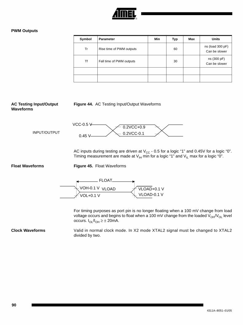
PWM Outputs
AC Testing Input/Output Waveforms
Figure 44. AC Testing Input/Output Waveforms
AC inputs during testing are driven at VCC - 0.5 for a logic “1” and 0.45V for a logic “0”.Timing measurement are made at VIH min for a logic “1” and VIL max for a logic “0”.
Float Waveforms Figure 45. Float Waveforms
For timing purposes as port pin is no longer floating when a 100 mV change from loadvoltage occurs and begins to float when a 100 mV change from the loaded VOH/VOL leveloccurs. IOL/IOH ≥ ± 20mA.
Clock Waveforms Valid in normal clock mode. In X2 mode XTAL2 signal must be changed to XTAL2divided by two.
Symbol Parameter Min Typ Max Units
Tr Rise time of PWM outputs 60 ns (load 300 pF)
Can be slower
Tf Fall time of PWM outputs 30 ns (300 pF)
Can be slower
0.45 V
VCC-0.5 V0.2VCC+0.9
0.2VCC-0.1INPUT/OUTPUT
VOL+0.1 V
VOH-0.1 V
FLOAT
VLOAD VLOAD+0.1 VVLOAD-0.1 V
904311A–8051–01/05

Figure 46. Clock Waveforms
This diagram indicates when signals are clocked internally. The time it takes the signalsto propagate to the pins, however, ranges from 25 to 125 ns. This propagation delay isdependent on variables such as temperature and pin loading. Propagation also variesfrom output to output and component. Typically though (TA=25°C fully loaded) RD andWR propagation delays are approximately 50 ns. The other signals are typically 85 ns.Propagation delays are incorporated in the AC specifications.
CLOCK
XTAL2
INTERNAL STATE4 STATE5 STATE6 STATE1 STATE2 STATE3 STATE4 STATE5
SERIAL PORT SHIFT CLOCK
PORT OPERATION
TXD (MODE 0)
RXD SAMPLED RXD SAMPLED
P1, P3, P4 PINS SAMPLEDP1, P3, P4 PINS SAMPLEDMOV DEST PORT (P1, P3, P4)(INCLUDES INT0, INT1, TO, T1)
OLD DATA NEW DATA
P1P2 P1P2 P1P2 P1P2 P1P2 P1P2 P1P2 P1P2
914311A–8051–01/05

Typical Application
Figure 47. Typical Application Diagram
Digital I/O
VCC
R C
EE
P3.5/W1M0
P3.4/T0/AIN5 NC
PFC control
P3.6
P3.7
NC
VSS
VSS
VSS
VSS VSS
P3.3/W0M2/AIN4
P3.2/INT0
P3.1/W0M1
P3.0/W0M0 Lamp driver high
Lamp driver low
Over current
NC
P4.3/AIN3
P4.2/AIN2
P4.1/AIN1
P4.0/AIN0PFC measurement
DC voltage
Lamp detection
Lamp currentAnalog I/O
RST
NC XTAL1
NC XTAL2
VCC
VREFVref
Vssa
Vcca
934311A–8051–01/05

Ordering InformationTable 7. Possible Order Entries
Part Number Memory
SizeSupply Voltage
Temperature Range Max Frequency Package Packing
AT83EB5114xxxTGRIL 4Kb ROM 3 to 3.6V Industrial 40 MHz S020 Reel
AT89EB5114-TGSIL 4Kb Flash 3 to 3.6V Industrial 40 MHz SO20 Stick
944311A–8051–01/05

Package Drawings
SO20
954311A–8051–01/05
Printed on recycled paper.
Disclaimer: Atmel Corporation makes no warranty for the use of its products, other than those expressly contained in the Company’s standardwarranty which is detailed in Atmel’s Terms and Conditions located on the Company’s web site. The Company assumes no responsibility for anyerrors which may appear in this document, reserves the right to change devices or specifications detailed herein at any time without notice, anddoes not make any commitment to update the information contained herein. No licenses to patents or other intellectual property of Atmel aregranted by the Company in connection with the sale of Atmel products, expressly or by implication. Atmel’s products are not authorized for useas critical components in life support devices or systems.
Atmel Corporation Atmel Operations
2325 Orchard ParkwaySan Jose, CA 95131Tel: 1(408) 441-0311Fax: 1(408) 487-2600
Regional Headquarters
EuropeAtmel SarlRoute des Arsenaux 41Case Postale 80CH-1705 FribourgSwitzerlandTel: (41) 26-426-5555Fax: (41) 26-426-5500
AsiaRoom 1219Chinachem Golden Plaza77 Mody Road TsimshatsuiEast KowloonHong KongTel: (852) 2721-9778Fax: (852) 2722-1369
Japan9F, Tonetsu Shinkawa Bldg.1-24-8 ShinkawaChuo-ku, Tokyo 104-0033JapanTel: (81) 3-3523-3551Fax: (81) 3-3523-7581
Memory2325 Orchard ParkwaySan Jose, CA 95131Tel: 1(408) 441-0311Fax: 1(408) 436-4314
Microcontrollers2325 Orchard ParkwaySan Jose, CA 95131Tel: 1(408) 441-0311Fax: 1(408) 436-4314
La ChantrerieBP 7060244306 Nantes Cedex 3, FranceTel: (33) 2-40-18-18-18Fax: (33) 2-40-18-19-60
ASIC/ASSP/Smart CardsZone Industrielle13106 Rousset Cedex, FranceTel: (33) 4-42-53-60-00Fax: (33) 4-42-53-60-01
1150 East Cheyenne Mtn. Blvd.Colorado Springs, CO 80906Tel: 1(719) 576-3300Fax: 1(719) 540-1759
Scottish Enterprise Technology ParkMaxwell BuildingEast Kilbride G75 0QR, Scotland Tel: (44) 1355-803-000Fax: (44) 1355-242-743
RF/AutomotiveTheresienstrasse 2Postfach 353574025 Heilbronn, GermanyTel: (49) 71-31-67-0Fax: (49) 71-31-67-2340
1150 East Cheyenne Mtn. Blvd.Colorado Springs, CO 80906Tel: 1(719) 576-3300Fax: 1(719) 540-1759
Biometrics/Imaging/Hi-Rel MPU/High Speed Converters/RF Datacom
Avenue de RochepleineBP 12338521 Saint-Egreve Cedex, FranceTel: (33) 4-76-58-30-00Fax: (33) 4-76-58-34-80
Web Sitehttp://www.atmel.com
4311A–8051–01/05 /xM
© Atmel Corporation 2004. All rights reserved. Atmel®, logo and combinations thereof are registered trademarks, and Everywhere You Are(SM)are the trademarks of Atmel Corporation or its subsidiaries. Other terms and product names may be trademarks of others.