low-power cmos relaxation oscillator design with an on ...1252/... · low-power cmos relaxation...
TRANSCRIPT
Low-Power CMOS Relaxation Oscillator Design with an On-Chip Circuit
for Combined Temperature-Compensated Reference Voltage and Current Generation
A Thesis Presented
by
Yuchi Ni
to
The Department of Electrical and Computer Engineering
in partial fulfillment of the requirements
for the degree of
Master of Science
in
Electrical Engineering
Northeastern University
Boston, Massachusetts
November, 2013
i
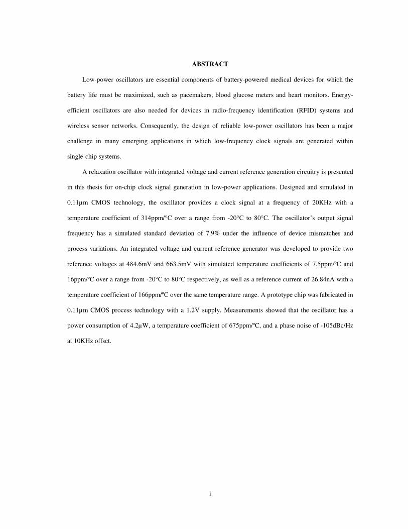
ABSTRACT
Low-power oscillators are essential components of battery-powered medical devices for which the
battery life must be maximized, such as pacemakers, blood glucose meters and heart monitors. Energy-
efficient oscillators are also needed for devices in radio-frequency identification (RFID) systems and
wireless sensor networks. Consequently, the design of reliable low-power oscillators has been a major
challenge in many emerging applications in which low-frequency clock signals are generated within
single-chip systems.
A relaxation oscillator with integrated voltage and current reference generation circuitry is presented
in this thesis for on-chip clock signal generation in low-power applications. Designed and simulated in
0.11µm CMOS technology, the oscillator provides a clock signal at a frequency of 20KHz with a
temperature coefficient of 314ppm/°C over a range from -20°C to 80°C. The oscillator’s output signal
frequency has a simulated standard deviation of 7.9% under the influence of device mismatches and
process variations. An integrated voltage and current reference generator was developed to provide two
reference voltages at 484.6mV and 663.5mV with simulated temperature coefficients of 7.5ppm/ºC and
16ppm/ºC over a range from -20°C to 80°C respectively, as well as a reference current of 26.84nA with a
temperature coefficient of 166ppm/ºC over the same temperature range. A prototype chip was fabricated in
0.11µm CMOS process technology with a 1.2V supply. Measurements showed that the oscillator has a
power consumption of 4.2µW, a temperature coefficient of 675ppm/ºC, and a phase noise of -105dBc/Hz
at 10KHz offset.

ii
ACKNOWLEDGMENTS
Firstly, I would like to express my gratitude to my advisor, Prof. Marvin Onabajo, for his patient
guidance and constructive suggestions. He not only showed me the art of analog IC design, but also taught
me how to be professional. He has broadened my mind, helped me to develop my future career, and he
will always be one of my role models. I also want to thank Prof. Yong-Bin Kim for providing access to the
silicon area for the prototype chip fabrication in 0.11µm CMOS technology through his research sponsor
Techwin Corp. My sincere appreciation goes to the members of the AMSIC research group and the
HPVLSI group at Northeastern University for their help and discussions, especially: Chun-hsiang Chang,
Hari Chauhan, Junpeng Feng, Seyed Alireza Zahrai, Jing Lu, Jing Yang, Yongsuk Choi, Inseok Jung, and
Ho Joon Lee.
I would like to thank my aunt Yanli He, who let me live with her when I arrived in the United States
for the first time. Her help and suggestions made my life in Boston much easier. I also want to thank my
friends, namely He Qi, Wei Cai, Weifu Li, Wei Wei, Wei Li, Zijian Chen, Ke Chen, Linbin Chen, Chenye
Yang and so on, for the happy memories at Northeastern University.
At last, my gratitude goes to my dear parents for their love and support. I could not have made it so
far without their help and encouragement.
iii
TABLE OF CONTENTS
Page
ABSTRACT ................................................................................................................................................... i
ACKNOWLEDGMENTS ............................................................................................................................. ii
TABLE OF CONTENTS ............................................................................................................................. iii
LIST OF FIGURES ...................................................................................................................................... iv
LIST OF TABLES ...................................................................................................................................... vii
1. INTRODUCTION ..................................................................................................................................... 1
1.1. Application overview ....................................................................................................................... 1
1.2. Low-power low-frequency oscillators .............................................................................................. 4
1.3. Research overview and contribution ................................................................................................ 7
2. CIRCUIT DESIGN AND ANALYSIS ..................................................................................................... 8
2.1. System-level overview ..................................................................................................................... 8
2.2. Reference voltage generation ........................................................................................................... 9
2.2.1. Negative temperature coefficient voltage ........................................................................... 10
2.2.2. Positive temperature coefficient voltage ............................................................................ 11
2.2.3. Bandgap reference .............................................................................................................. 12
2.2.4. Implementation of a bandgap reference using a proportional-to-absolute temperature
current ............................................................................................................................. 13
2.2.5. Voltage reference circuit consisting of subthreshold MOSFETs ........................................ 15
2.3. Reference current generation .......................................................................................................... 19
2.3.1. Temperature-independent current generation ..................................................................... 19
2.3.2. Proposed temperature-independent current and voltage reference...................................... 28
2.4. Comparator design .......................................................................................................................... 30
2.4.1. Open-loop comparator ........................................................................................................ 32
2.5. Switch design ................................................................................................................................. 34
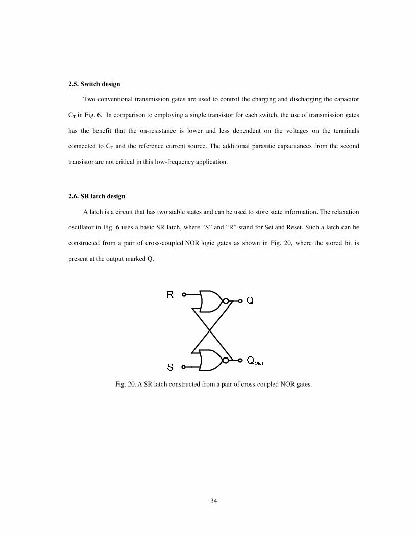
2.6. SR latch design ............................................................................................................................... 34
3. SIMULATION RESULTS ...................................................................................................................... 37
3.1. Reference generator simulation results ........................................................................................... 37
3.2. Comparator simulation results ........................................................................................................ 45
3.3. Oscillator simulations ..................................................................................................................... 47
4. CHIP LAYOUT DESIGN, PCB DESIGN AND MEASURMENT RESULTS ..................................... 51
5. CONCLUSIONS AND FUTURE WORK .............................................................................................. 65
5.1. Conclusion ...................................................................................................................................... 65
5.2. Future work .................................................................................................................................... 65
REFERENCES ............................................................................................................................................ 66
iv
LIST OF FIGURES
Page
Fig. 1. Simplified block diagram of an RFID transponder. .............................................................. 1
Fig. 2. Cardiac pacemaker system [3]. ............................................................................................. 3
Fig. 3. Block diagram of an implantable cardiac pacemaker system. .............................................. 4
Fig. 4. Typical commercial crystal oscillator. .................................................................................. 5
Fig. 5. Diagram of a simple 3-inverter ring oscillator. ..................................................................... 5
Fig. 6. Relaxation oscillator block diagram. .................................................................................... 8
Fig. 7. Generation of a proportional-to-absolute temperature voltage. .......................................... 12
Fig. 8. A bandgap reference circuit (from [16]). ............................................................................ 13
Fig. 9. Generation of a bandgap reference voltage using a PTAT current [15]. ............................. 14
Fig. 10. Ultra-low power voltage reference circuit from [17]. ......................................................... 15
Fig. 11. Current reference circuit with subthreshold CMOS devices. .............................................. 20
Fig. 12. Current reference circuit using subthreshold MOS resistor ladder. .................................... 23
Fig. 13. Subthreshold MOS resistor ladder consisting of N MOSFETs. .......................................... 25
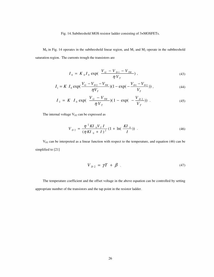
Fig. 14. Subthreshold MOS resistor ladder consisting of 3×MOSFETs. ......................................... 26
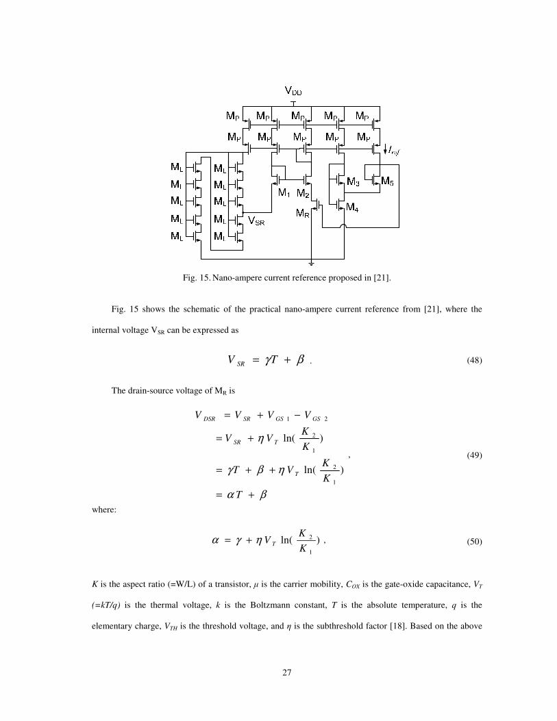
Fig. 15. Nano-ampere current reference proposed in [21]. .............................................................. 27
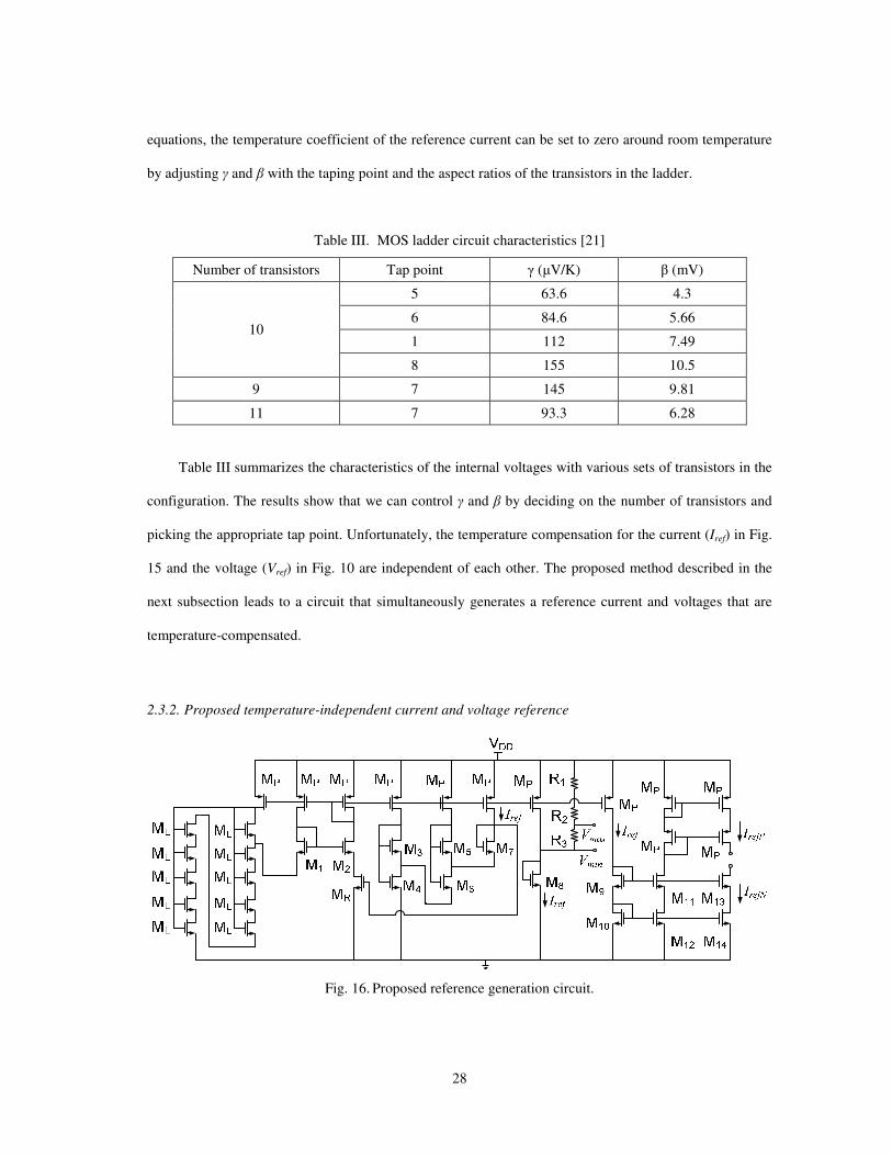
Fig. 16. Proposed reference generation circuit. ................................................................................ 28
Fig. 17. Ideal comparator transfer function. ..................................................................................... 31
Fig. 18. Non-ideal comparator transfer function. ............................................................................. 31
Fig. 19. Open-loop comparator. ....................................................................................................... 32
Fig. 20. A SR latch constructed from a pair of cross-coupled NOR gates. ...................................... 34
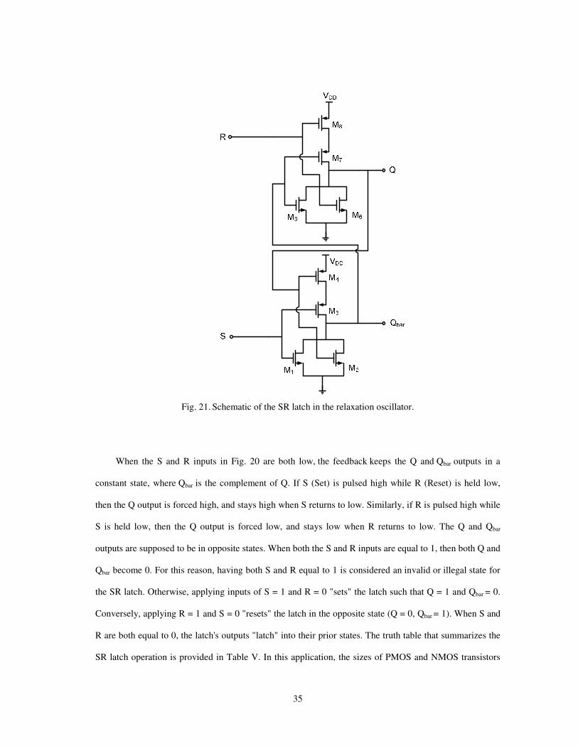
Fig. 21. Schematic of the SR latch in the relaxation oscillator......................................................... 35
Fig. 22. Simulated reference current (Iref in Fig. 16) vs. temperature. .............................................. 39
Fig. 23. Simulated reference voltage Vmax vs. temperature............................................................... 39
Fig. 24. Simulated reference voltage Vmin vs. temperature. .............................................................. 40
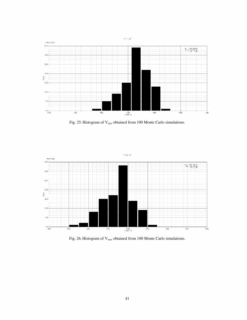
Fig. 25. Histogram of Vmin obtained from 100 Monte Carlo simulations......................................... 41

v
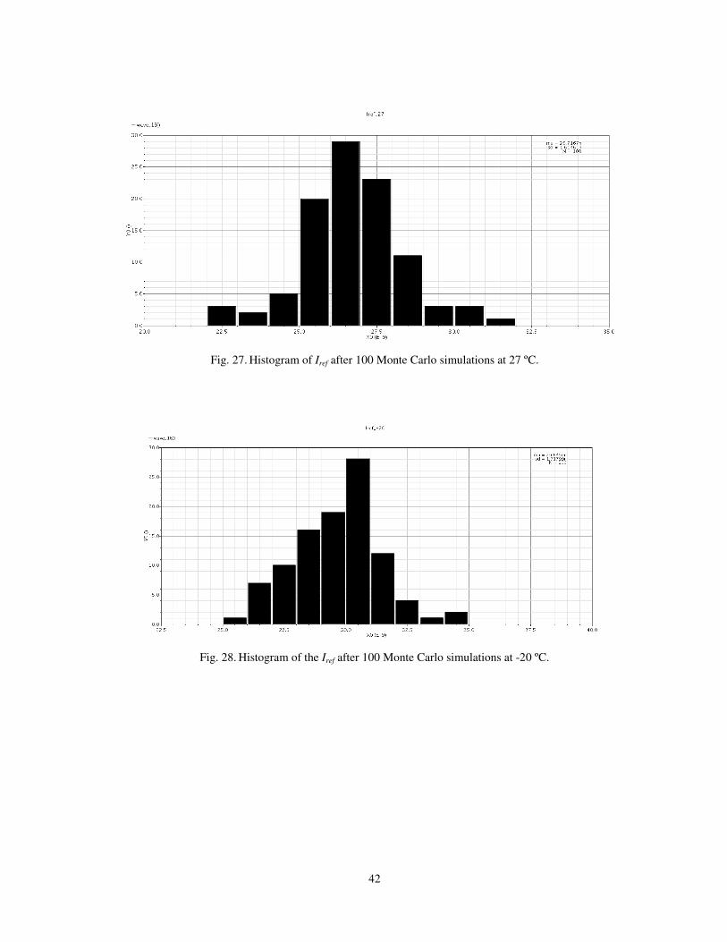
Fig. 26. Histogram of Vmax obtained from 100 Monte Carlo simulations. ....................................... 41
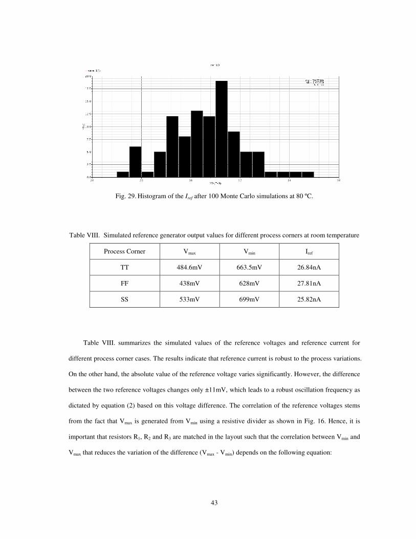
Fig. 27. Histogram of Iref after 100 Monte Carlo simulations at 27 ºC. ............................................ 42
Fig. 28. Histogram of the Iref after 100 Monte Carlo simulations at -20 ºC. .................................... 42
Fig. 29. Histogram of the Iref after 100 Monte Carlo simulations at 80 ºC. ...................................... 43
Fig. 30. Simulated open-loop gain and phase shift vs. frequency of the amplifier used as
comparator. ......................................................................................................................... 45
Fig. 31. Histogram of the comparator’s input-referred offset voltage obtained with 100 Monte Carlo
simulations. ......................................................................................................................... 46
Fig. 32. Simulated output waveform at node Q’ with 5pF load capacitance. ................................... 47
Fig. 33. Simulated oscillation frequency vs. temperature. ............................................................... 48
Fig. 34. Histogram of the oscillation frequency obtained from 100 Monte Carlo simulations. ....... 48
Fig. 35. Simulated oscillator phase noise. ........................................................................................ 49
Fig. 36. RMS period jitter simulation result. .................................................................................... 49
Fig. 37. Oscillator chip layout. ......................................................................................................... 51
Fig. 38. Die micrograph of the prototype chip. ................................................................................ 51
Fig. 39. Screenshot of the PCB schematic. ...................................................................................... 52
Fig. 40. PCB schematic. ................................................................................................................... 53
Fig. 41. PCB layout. ......................................................................................................................... 54
Fig. 42. PCB and measurement equipment. ..................................................................................... 55
Fig. 43. Experimental setup. ............................................................................................................ 56
Fig. 44. Measured output waveform of the oscillator chip using on-chip references. ...................... 57
Fig. 45. Schematic to evaluate reference current deviation. ............................................................. 58
Fig. 46. Simulated reference current vs. threshold voltage change of transistor MR. ....................... 58
Fig. 47. Replacing MR with components with multiplier. ................................................................ 59
Fig. 48. Histogram of the Iref obtained with 100 Monte Carlo simulations after replacing MR with
multiple devices. ................................................................................................................. 59
Fig. 49. Measured phase noise with off-chip current/voltage references. ........................................ 60
vi
Fig. 50. Measured RMS period jitter with off-chip current/voltage references. .............................. 61
Fig. 51. Measured phase noise with on-chip current/voltage references. ......................................... 61
Fig. 52. Measured RMS period jitter with on-chip current/voltage references. ............................... 62
Fig. 53. Measured oscillation frequency vs. temperature. ................................................................ 64
vii
LIST OF TABLES
Page
Table I. RFID frequency bands .......................................................................................................... 2
Table II. Comparisons of different types of oscillators ....................................................................... 6
Table III. MOS ladder circuit characteristics [21] .............................................................................. 28
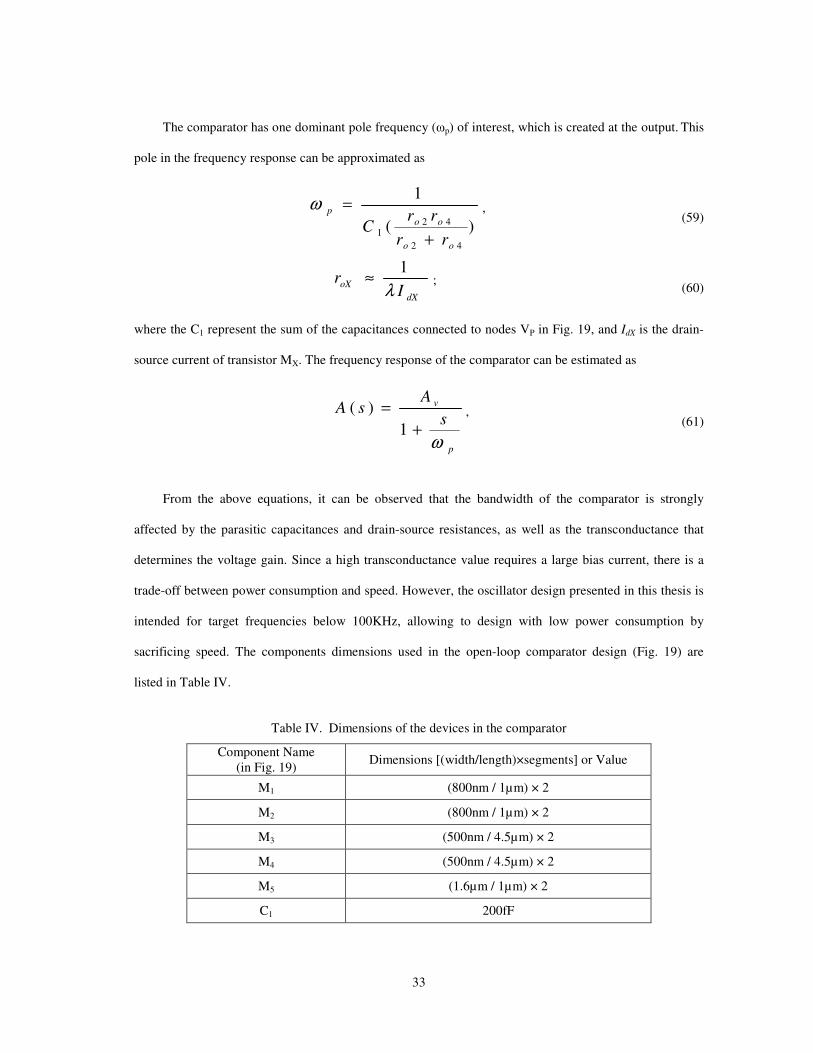
Table IV. Dimensions of the devices in the comparator ..................................................................... 33
Table V. Truth table of the SR latch .................................................................................................. 36
Table VI. Dimensions of the devices in the SR latch .......................................................................... 36
Table VII. Design parameters of proposed reference current/voltage generator and the relaxation
oscillator (0.11µm CMOS, 1.2V supply) ............................................................................ 38
Table VIII. Simulated reference generator output values for different process corners at room
temperature ......................................................................................................................... 43
Table IX. Comparison with other reference generation circuits ......................................................... 44
Table X. Simulated open-loop comparator specifications ................................................................. 46
Table XI. Comparison with other reported oscillators ........................................................................ 50
Table XII. Oscillation frequencies for different off-chip reference currents ........................................ 57
Table XIII. Comparison of test chip measurement results with other designs ....................................... 62
Table XIV. On-chip reference voltages and the oscillation frequencies at different temperatures ........ 64
1
1. INTRODUCTION
1.1. Application overview
The demand for low-power integrated circuits is continuing to increase in applications such as
wireless sensor networks, energy harvesting, battery-operated medical devices (e.g., pacemakers [1]-[3]
and blood glucose meters), as well as radio-frequency identification (RFID) systems [4]-[6]. Ideally, the
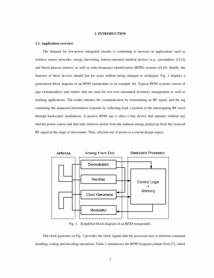
batteries of these devices should last for years without being changed or recharged. Fig. 1 displays a
generalized block diagram of an RFID transponder as an example [6]. Typical RFID systems consist of
tags (transponders) and readers that are used for low-cost automated inventory management as well as
tracking applications. The reader initiates the communication by transmitting an RF signal, and the tag
containing the requested information responds by reflecting back a portion of the interrogating RF wave
through backscatter modulation. A passive RFID tag is often a tiny device that operates without any
internal power source and that only retrieves power from the induced energy picked up from the received
RF signal in the range of microwatts. Thus, efficient use of power is a crucial design aspect.
Fig. 1. Simplified block diagram of an RFID transponder.
The clock generator in Fig. 1 provides the clock signals that the processor uses to perform command
handling, coding and decoding operations. Table 1 summarizes the RFID frequency bands from [7], which

2
shows that the transmit/receive frequencies can vary from several kilohertz to gigahertz depending on the
application.
Many RFID transponders are in standby mode most of the time, and are woken up at regular intervals
for a short time to perform measurements or communication tasks with the help of clock signals from on-
chip oscillators. Afterwards, the system is placed into a power-down mode with minimal power
consumption to preserve the available battery capacity [8]. In this and the other similar applications
mentioned previously, low-power consumption is one of the most important design considerations.
Table I. RFID frequency bands
Frequency Range Data Speed Remarks Regulation
<135 KHz 10cm Low Identification and
Tracking Unregulated
13.56 MHz 1m Low to moderate Smart Cards ISM Band
Worldwide
433 MHz 1–100m Moderate Defense
Applications
Short Range
Devices
865-868 MHz
(Europe)
902-928 MHz
(North America)
1–2m Moderate to
High
EAN, Various
Standards ISM band
2450-5800 MHz 1–2m High 802.11 WLAN,
Bluetooth ISM band
Implantable and portable medical systems span a number of different target applications and are
widely used in the therapy. Traditionally, bradycardia pacemakers and tachyarrthymia defibrillators are the
largest markets. Pacemakers are used to treat bradyarrhythmia (a heart rate that is too slow) by monitoring
the heart’s rate (how fast it beats) and rhythm (the pattern in which it beats), and by providing electrical

3
stimulation when the heart does not beat properly [3]. A pacemaker system, as shown in Fig. 2, generally
consists of two components: pacing leads and pacemaker device.
Fig. 2. Cardiac pacemaker system [3].
Inserted through a vein into the heart, pacing leads carry impulses from the pacemaker device to the
heart, stimulating the heart to beat. They also carry information from the heart back to the device, which is
used to assess the status of the patient’s heart.
Implantable devices such as pacemakers have traditionally used a non-rechargeable battery as the
energy source for the system. With this approach, longevity becomes a desirable characteristic,
minimizing the patient’s exposure to implantation surgery. The battery is typically made of lithium iodine,
which gives a life span of up to 10-12 years.
4
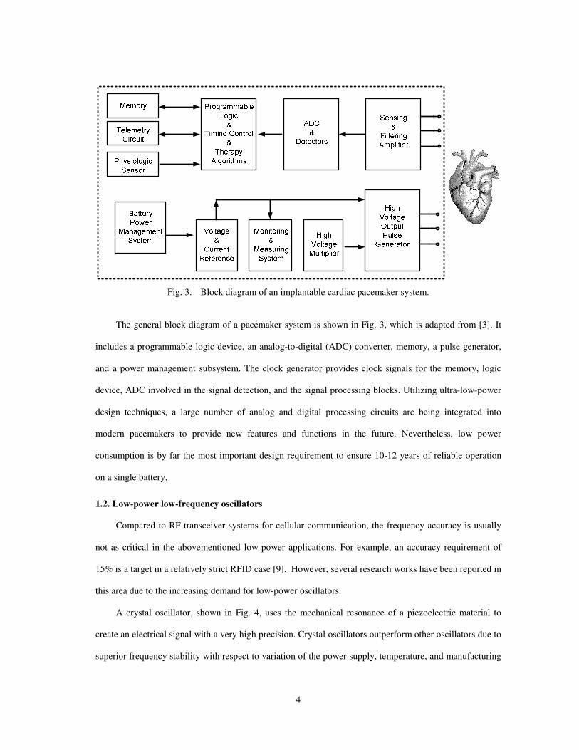
Fig. 3. Block diagram of an implantable cardiac pacemaker system.
The general block diagram of a pacemaker system is shown in Fig. 3, which is adapted from [3]. It
includes a programmable logic device, an analog-to-digital (ADC) converter, memory, a pulse generator,
and a power management subsystem. The clock generator provides clock signals for the memory, logic
device, ADC involved in the signal detection, and the signal processing blocks. Utilizing ultra-low-power
design techniques, a large number of analog and digital processing circuits are being integrated into
modern pacemakers to provide new features and functions in the future. Nevertheless, low power
consumption is by far the most important design requirement to ensure 10-12 years of reliable operation
on a single battery.
1.2. Low-power low-frequency oscillators
Compared to RF transceiver systems for cellular communication, the frequency accuracy is usually
not as critical in the abovementioned low-power applications. For example, an accuracy requirement of
15% is a target in a relatively strict RFID case [9]. However, several research works have been reported in
this area due to the increasing demand for low-power oscillators.
A crystal oscillator, shown in Fig. 4, uses the mechanical resonance of a piezoelectric material to
create an electrical signal with a very high precision. Crystal oscillators outperform other oscillators due to
superior frequency stability with respect to variation of the power supply, temperature, and manufacturing
5
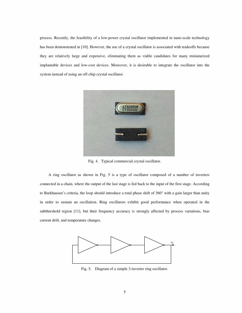
process. Recently, the feasibility of a low-power crystal oscillator implemented in nano-scale technology
has been demonstrated in [10]. However, the use of a crystal oscillator is associated with tradeoffs because
they are relatively large and expensive, eliminating them as viable candidates for many miniaturized
implantable devices and low-cost devices. Moreover, it is desirable to integrate the oscillator into the
system instead of using an off-chip crystal oscillator.
Fig. 4. Typical commercial crystal oscillator.
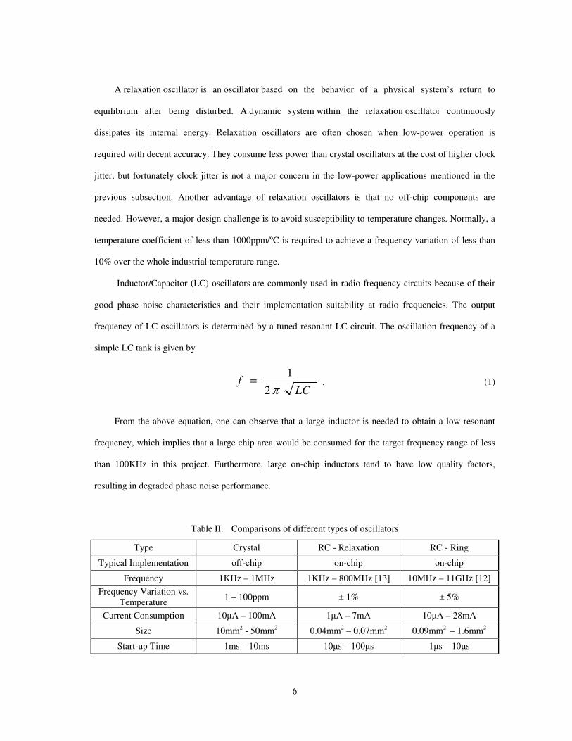
A ring oscillator as shown in Fig. 5 is a type of oscillator composed of a number of inverters
connected in a chain, where the output of the last stage is fed back to the input of the first stage. According
to Barkhausen’s criteria, the loop should introduce a total phase shift of 360° with a gain larger than unity
in order to sustain an oscillation. Ring oscillators exhibit good performance when operated in the
subthreshold region [11], but their frequency accuracy is strongly affected by process variations, bias
current drift, and temperature changes.
Fig. 5. Diagram of a simple 3-inverter ring oscillator.
6
A relaxation oscillator is an oscillator based on the behavior of a physical system’s return to
equilibrium after being disturbed. A dynamic system within the relaxation oscillator continuously
dissipates its internal energy. Relaxation oscillators are often chosen when low-power operation is
required with decent accuracy. They consume less power than crystal oscillators at the cost of higher clock
jitter, but fortunately clock jitter is not a major concern in the low-power applications mentioned in the
previous subsection. Another advantage of relaxation oscillators is that no off-chip components are
needed. However, a major design challenge is to avoid susceptibility to temperature changes. Normally, a
temperature coefficient of less than 1000ppm/ºC is required to achieve a frequency variation of less than
10% over the whole industrial temperature range.
Inductor/Capacitor (LC) oscillators are commonly used in radio frequency circuits because of their
good phase noise characteristics and their implementation suitability at radio frequencies. The output
frequency of LC oscillators is determined by a tuned resonant LC circuit. The oscillation frequency of a
simple LC tank is given by
LCf
π2
1= . (1)
From the above equation, one can observe that a large inductor is needed to obtain a low resonant
frequency, which implies that a large chip area would be consumed for the target frequency range of less
than 100KHz in this project. Furthermore, large on-chip inductors tend to have low quality factors,
resulting in degraded phase noise performance.
Table II. Comparisons of different types of oscillators
Type Crystal RC - Relaxation RC - Ring
Typical Implementation off-chip on-chip on-chip
Frequency 1KHz – 1MHz 1KHz – 800MHz [13] 10MHz – 11GHz [12]
Frequency Variation vs.
Temperature 1 – 100ppm ± 1% ± 5%
Current Consumption 10µA – 100mA 1µA – 7mA 10µA – 28mA
Size 10mm2 - 50mm
2 0.04mm
2 – 0.07mm
2 0.09mm
2 – 1.6mm
2
Start-up Time 1ms – 10ms 10µs – 100µs 1µs – 10µs

7
Table II lists typical characteristics of different types of oscillators. For highly-integrated low-power
devices, crystal oscillators are often avoided because of their high power consumption and printed-circuit
board area requirement. From the view of power and area efficiency of on-chip implementations,
relaxation oscillators and ring oscillators are comparable, but further comparison reveals that relaxation
oscillators often outperform ring oscillators in low-frequency applications in terms of accuracy and area
efficiency because low-frequency ring oscillators require a large number of stages. In consideration of the
stringent power and area limitations of the target applications, a relaxation oscillator architecture was
chosen to improve the state-of-the-art with this research effort.
1.3. Research overview and contribution
In this thesis, a relaxation oscillator with integrated voltage and current reference generation circuitry
is presented for on-chip clock signal generation in low-power applications. A novel feature of the
integrated voltage and current reference generator is that it has been developed to simultaneously provide
two temperature-independent voltages and one temperature-independent current for the oscillator.
Designed in standard 0.11µm CMOS technology, the oscillator provides a clock signal at the frequency of
20KHz with a simulated temperature coefficient of 314ppm/°C over a range from -20°C to 80°C. The
oscillator’s output signal frequency has a simulated standard deviation of 7.9% under the influence of
device mismatches and process variations. It operates with a supply voltage of 1.2V and has a simulated
dynamic power consumption of 4.9µW at room temperature. A chip fabricated in Dongbu 0.11µm CMOS
technology has a measured power consumption, temperature coefficient and phase noise of 4.2µW,
675ppm/ºC and -105dBc/Hz at 10KHz offset, respectively.
A study of temperature variation influence on the performance of relaxation oscillator circuitry was
conducted and is summarized in Chapter 2. Several temperature compensation techniques are discussed
and evaluated with simulations. A novel method is proposed that can compensate the generated reference
voltage and reference current simultaneously. Simulation results indicate that the proposed compensation
8
approach is robust to process variations and enables to achieve very low temperature coefficients, making
it suitable for reliable low-power relaxation oscillators. The remainder of this thesis is organized as
follows: in addition to describing the temperature compensation technique, Chapter 2 also focuses on the
design issues for the comparator and switches in the relaxation oscillator. Chapter 3 contains discussions
of simulation results and a description of chip layout considerations. The design of the printed circuit
board for the prototype chip, measurement setup, and measurement results are discussed in Chapter 4.
Finally, a summary and conclusions are provided in Chapter 5.
2. CIRCUIT DESIGN AND ANALYSIS
2.1. System-level overview
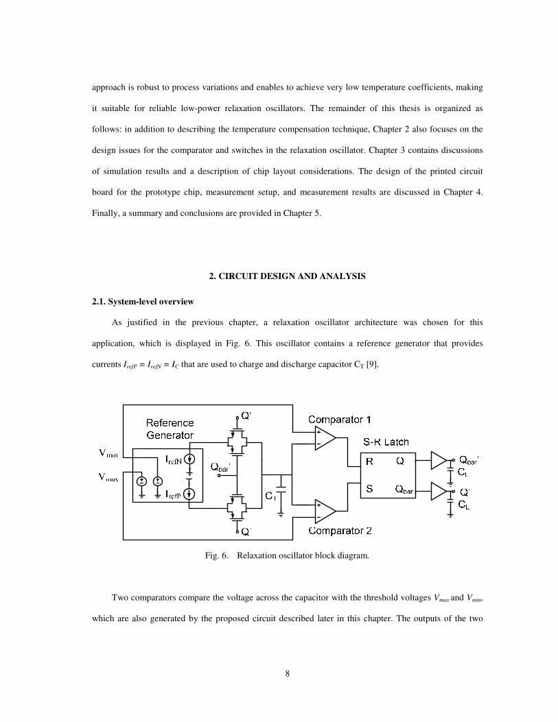
As justified in the previous chapter, a relaxation oscillator architecture was chosen for this
application, which is displayed in Fig. 6. This oscillator contains a reference generator that provides
currents IrefP = IrefN = IC that are used to charge and discharge capacitor CT [9].
Fig. 6. Relaxation oscillator block diagram.
Two comparators compare the voltage across the capacitor with the threshold voltages Vmax and Vmin,
which are also generated by the proposed circuit described later in this chapter. The outputs of the two

9
comparators are applied to an S-R latch to drive the transmission gates. When the voltage across the
capacitor rises above Vmax, then the output of Comparator 2 will transition to high, Q’ becomes 1 and Qbar’
becomes 0. Consequently, the transmission gate that connects to the current sink will turn on to discharge
CT. On the other hand, when the voltage across the capacitor falls below Vmin, the output of the comparator
1 changes to high, Q’ becomes 0 and Qbar’ becomes 1, and the capacitor will be charged. The frequency of
the resulting oscillation can be expressed as [9]:
)(2 minmax VVC
If
T
C
−= . (2)
From equation (2), we can conclude that a nano-scale current is a prerequisite condition for low-
frequency oscillation in the kilohertz range. Another observation is that a temperature-independent
oscillation signal requires temperature-compensated current and voltage references. Furthermore, the
generation of a nano-scale current typically requires that some transistors are biased in the subthreshold
region, which necessitates process variation-aware design [14]. Lastly, a load capacitor in the picofarad
range should be adopted to create an oscillation frequency in kilohertz range.
2.2. Reference voltage generation
Analog and mixed-signal integrated systems extensively incorporate voltage and current reference
circuits. These references should exhibit little dependence on temperature, process and supply voltage. For
example, the bias current of a differential amplifier must be generated reliably because it affects the
voltage gain, noise, and other critical parameters. In systems such as analog-to-digital converters and
digital-to-analog converters, precise reference voltages or currents are typically required to quantize the
input signals. In the discussed relaxation oscillator, the generation of temperature-insensitive reference
voltages and currents is the prerequisite condition for a temperature-independent oscillation. The basic
concept behind generating a temperature-independent reference is that if two quantities having opposite
temperature coefficients are added with proper weighting, the result displays a zero temperature
coefficient. For example, for two voltages V1 and V2 that change in opposite directions with temperature,
10
we can choose α1 and α2 so that α1·∂V1/∂T + α2·∂V2/∂T = 0, obtaining a reference voltage of Vref = α1V1 +
α2V2 that has a temperature coefficient of zero. Next, voltages that have positive and negative temperature
coefficients will be examined.
2.2.1. Negative temperature coefficient voltage
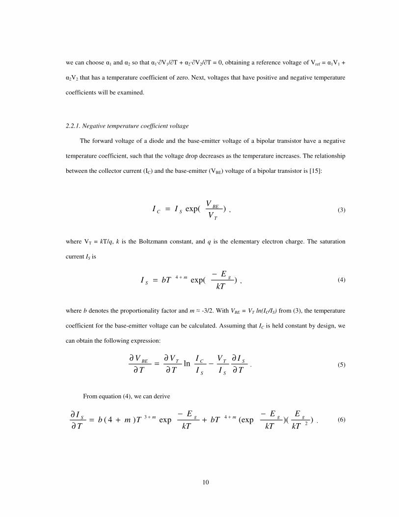
The forward voltage of a diode and the base-emitter voltage of a bipolar transistor have a negative
temperature coefficient, such that the voltage drop decreases as the temperature increases. The relationship
between the collector current (IC) and the base-emitter (VBE) voltage of a bipolar transistor is [15]:
)exp(T
BESC
V
VII = , (3)
where VT = kT/q, k is the Boltzmann constant, and q is the elementary electron charge. The saturation
current IS is
)exp(4
kT
EbTI
gm
S
−= +
, (4)
where b denotes the proportionality factor and m ≈ -3/2. With VBE = VT ln(IC/IS) from (3), the temperature
coefficient for the base-emitter voltage can be calculated. Assuming that IC is held constant by design, we
can obtain the following expression:
T
I
I
V
I
I
T
V
T
V S
S
T
S
CTBE
∂
∂−
∂
∂=
∂
∂ln . (5)
From equation (4), we can derive
))((expexp)4(2
43
kT
E
kT
EbT
kT
ETmb
T
I ggmgmS−
+−
+=∂
∂ ++. (6)
11
Hence,
T
gTS
S
T VkT
E
T
Vm
T
I
I
V2
)4( ++=∂
∂. (7)
With the aid of (5) and (7) it can be shown that [15]:
T
qEVmV
T
V gTBEBE/)4( −+−
=∂
∂. (8)
Equation (8) is the temperature coefficient of the base-emitter voltage at a given temperature. With
VBE = 750mV and T = 300ºK for instance, ∂VBE/∂T = -1.5mV/ºK. It is quite interesting to notice that the
temperature coefficient itself varies with temperature. If the base-emitter voltage is added to a voltage with
a constant positive temperature coefficient, then an overall temperature coefficient of zero can only be
achieved around a specific temperature.
2.2.2. Positive temperature coefficient voltage
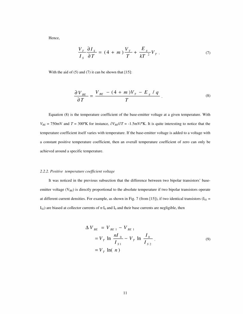
It was noticed in the previous subsection that the difference between two bipolar transistors’ base-
emitter voltage (VBE) is directly proportional to the absolute temperature if two bipolar transistors operate
at different current densities. For example, as shown in Fig. 7 (from [15]), if two identical transistors (IS1 =
IS2) are biased at collector currents of n·I0 and I0 and their base currents are negligible, then
)ln(
lnln2
0
1
0
11
nV
I
IV
I
nIV
VVV
T
S
T
S
T
BEBEBE
=
−=
−=∆
. (9)
12
Based on equation (9), we can write
)ln(nq
k
T
VBE =∂
∆∂. (10)
Equation (10) indicates that the VBE difference exhibits a positive temperature coefficient.
Fig. 7. Generation of a proportional-to-absolute temperature voltage.
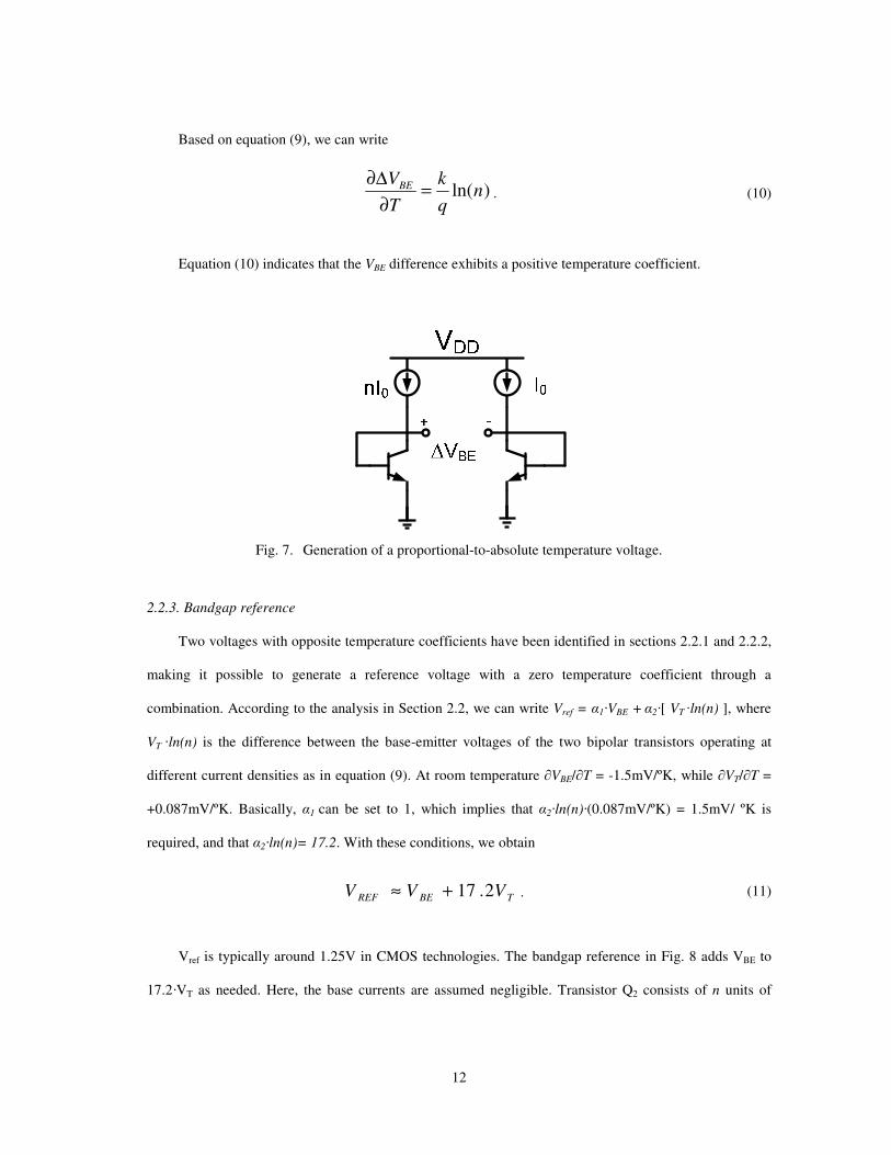
2.2.3. Bandgap reference
Two voltages with opposite temperature coefficients have been identified in sections 2.2.1 and 2.2.2,
making it possible to generate a reference voltage with a zero temperature coefficient through a
combination. According to the analysis in Section 2.2, we can write Vref = α1·VBE + α2·[ VT ·ln(n) ], where
VT ·ln(n) is the difference between the base-emitter voltages of the two bipolar transistors operating at
different current densities as in equation (9). At room temperature ∂VBE/∂T = -1.5mV/ºK, while ∂VT/∂T =
+0.087mV/ºK. Basically, α1 can be set to 1, which implies that α2·ln(n)·(0.087mV/ºK) = 1.5mV/ ºK is
required, and that α2·ln(n)= 17.2. With these conditions, we obtain
TBEREF VVV 2.17+≈ . (11)
Vref is typically around 1.25V in CMOS technologies. The bandgap reference in Fig. 8 adds VBE to
17.2·VT as needed. Here, the base currents are assumed negligible. Transistor Q2 consists of n units of
13
transistors in parallel, and Q1 is a unit transistor. Nodes X and Y are forced to be equal as a result of the
operational amplifier feedback.
Fig. 8. A bandgap reference circuit (from [16]).
The reference voltage in Fig. 8 is generated at the output of the amplifier, which can be expressed as:
)1()ln(
)()ln(
3
22
32
3
2
R
RnVV
RRR
nVVV
TBE
TBEout
+⋅+=
+⋅+=
. (12)
In order to achieve a zero temperature coefficient, the ratio of (1+R2/R3)·ln(n) should be set to
approximately 17.2. From equation (12), one can observe that the output voltage depends on the ratio of
the resistors instead of their absolute values, which makes the temperature coefficient of this voltage
robust to the temperature coefficient of the resistors and to process variations.
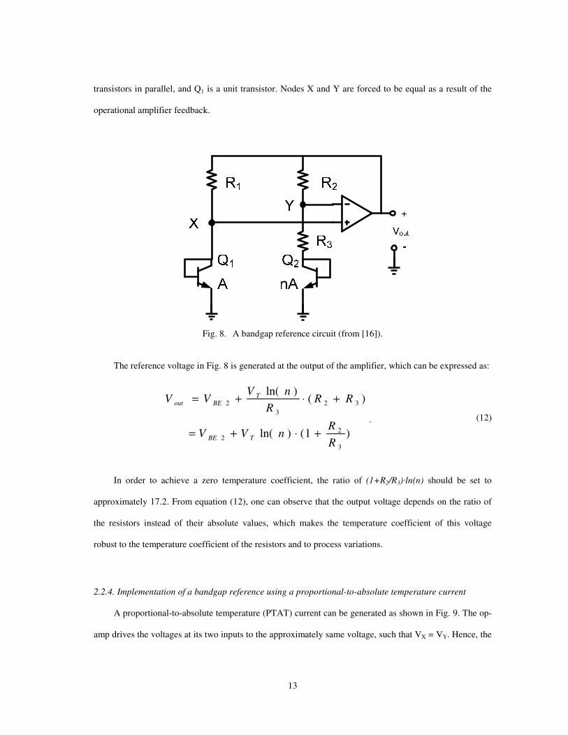
2.2.4. Implementation of a bandgap reference using a proportional-to-absolute temperature current
A proportional-to-absolute temperature (PTAT) current can be generated as shown in Fig. 9. The op-
amp drives the voltages at its two inputs to the approximately same voltage, such that VX = VY. Hence, the
14
voltage difference between node Y and the emitter of Q2 equals VT·ln(n), and the current in this branch is
VT·ln(n)/R1. This current is copied by the current mirror to generate the PTAT current at the drain of M3
that is equal to m·VT·ln(n)/R1, where m is the current mirror (M3, M2) ratio.
Q1 Q2
Q3
M2M1 M3
VDD
R1 R2
Vout
A nA
PTAT
Current
X Y
Fig. 9. Generation of a bandgap reference voltage using a PTAT current [15].
The equation for the output voltage in Fig. 9 can be expressed as
2
1
3
)ln(R
R
nVVV T
BEout += , (13)
where all the PMOS transistors are assumed to be identical. The size of Q3 and the values of R1 and R2 are
arbitrary as long as the sum of the two terms in equation (13) results in a zero temperature coefficient.
In summary, the bandgap reference is a highly reliable circuit with an output that is robust to
temperature and process variations. Nevertheless, there are some severe drawbacks of this circuit, making
it an inappropriate candidate for the application in this thesis. First, the bandgap reference voltage is
typically around 1.25 V, which is relatively high for modern sub-micron CMOS technologies. Second, the
power consumptions of conventional bandgap reference generators are usually in the microwatts range,

15
which is too high for ultra-low power systems. For the purpose of minimizing power, the resistances can
be increased to the megaohm range, which reduces the currents. However, such high resistances would
require large areas during on-chip implementations, which again would be unsuitable for the target
application. Given the stringent silicon area, power consumption and supply voltage limits, an alternative
reference voltage generation has been explored.
2.2.5. Voltage reference circuit consisting of subthreshold MOSFETs
One of the promising areas of research in analog circuit design is the development of ultra-low power
circuits with transistors operating in the subthreshold region by biasing them with a gate-source voltage
below the threshold voltage. For example, a voltage reference that can operate with sub-microwatt power
dissipation and low temperature sensitivity has been reported in [17], which consists of subthreshold
MOSFET devices. The basic principle is the generation of a voltage with a negative temperature
coefficient and another voltage with positive temperature coefficient, which are summed up to produce an
output voltage with a zero temperature coefficient.
Fig. 10. Ultra-low power voltage reference circuit from [17].
16
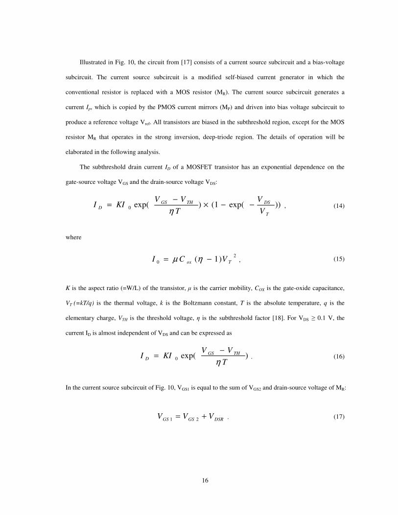
Illustrated in Fig. 10, the circuit from [17] consists of a current source subcircuit and a bias-voltage
subcircuit. The current source subcircuit is a modified self-biased current generator in which the
conventional resistor is replaced with a MOS resistor (MR). The current source subcircuit generates a
current Ip, which is copied by the PMOS current mirrors (MP) and driven into bias voltage subcircuit to
produce a reference voltage Vref. All transistors are biased in the subthreshold region, except for the MOS
resistor MR that operates in the strong inversion, deep-triode region. The details of operation will be
elaborated in the following analysis.
The subthreshold drain current ID of a MOSFET transistor has an exponential dependence on the
gate-source voltage VGS and the drain-source voltage VDS:
))exp(1()exp(0
T
DSTHGSD
V
V
T
VVKII −−×
−=
η, (14)
where
2
0 )1( Tox VCI −= ηµ , (15)
K is the aspect ratio (=W/L) of the transistor, µ is the carrier mobility, COX is the gate-oxide capacitance,
VT (=kT/q) is the thermal voltage, k is the Boltzmann constant, T is the absolute temperature, q is the
elementary charge, VTH is the threshold voltage, η is the subthreshold factor [18]. For VDS ≥ 0.1 V, the
current ID is almost independent of VDS and can be expressed as
)exp(0T
VVKII THGS
Dη
−= . (16)
In the current source subcircuit of Fig. 10, VGS1 is equal to the sum of VGS2 and drain-source voltage of MR:
DSRGSGS VVV += 21 . (17)
17
Assuming that the currents in M1 and M2 are equal due to matched dimensions in both branches, equations
(16) and (17) can be combined and rearranged to:
)ln(1
2
K
KVV TDSR η= , (18)
where K1 is the aspect ratio (W/L) of transistor M1, and K2 is the aspect ratio of transistor M2.
The MOS resistor MR is biased in strong inversion, deep triode region. Therefore, its resistance can
be expressed as
)(
1
1 THrefoxR
MRVVCK
R−
=µ
, (19)
where KR1 is the aspect ratio of transistor MR. From (18) and (19), it follows that
)ln()(1
21
K
KVVVCK
R
VI
TTHrefOXR
MR
DSRP
ηµ −=
=
. (20)
In the bias voltage subcircuit of Fig. 10, the gate-source voltages (VGS3 through VGS7) of the
transistors form a closed path, and the currents in M4 and M6 are 3·Ip and 2·Ip respectively. Therefore, the
output voltage Vref is
)2
ln()3
ln(
)2
ln(
76
53
04
76
53
4
75634
KK
KKV
IK
IVV
KK
KKVV
VVVVVV
T
p
TTH
TGS
GSGSGSGSGSref
ηη
η
++=
+=
+−+−=
. (21)

18
Equation (21) reveals that Vref is a sum of the threshold voltage and several scaled thermal voltages.
Since the threshold voltage has a negative temperature coefficient and the thermal voltage has a positive
temperature coefficient, the reference voltage can exhibit a zero temperature coefficient if the thermal
voltages are properly scaled. More specifically, the temperature dependence of the threshold can be
expressed as [17]
TVV THTH κ+= 0 , (22)
where VTH0 is the threshold voltage at 0º K, and κ is the temperature coefficient (TC) of the VTH. Using
equations (20) and (22), the output voltage Vref in (21) can be rewritten as
)ln(
)1(
)(6ln
1
2
764
531
0
K
K
VKKK
VVKKKV
TVV
T
THrefR
T
THref
−
−+
+=
η
ηη
κ
, (23)
and the TC of Vref can be expressed as
1
)(1
)ln()1(
)(6ln
1
2
764
531
TT
V
VVV
K
K
VKKK
VVKKK
q
k
T
V
ref
THref
T
T
THrefRBref
−+∂
∂
−+
−
−+−=
∂
∂
κη
η
ηηκ
. (24)
Assuming that Vref - VTH0 << κT and that ηT << κT, the TC of Vref can be simplified to:
)ln()1(
6ln
1
2
764
531
K
K
KKK
KKK
k
q
q
k
T
VR
B
Bref
−+−=
∂
∂
η
ηκηκ . (25)
A zero TC can be achieved by satisfying the following condition:
19
0)ln()1(
6ln
1
2
764
531 =−
+−K
K
KKK
KKK
k
q
q
k R
B
B
η
ηκηκ . (26)
If the transistors are properly ratioed according to equation (26), a zero TC reference voltage can be
generated using the circuit in Fig. 10. Based on the above equations, we can find that under the assumed
conditions:
0THref VV = . (27)
2.3. Reference current generation
Analog integrated systems incorporate current references extensively. Reference current generators
are widely used for amplifiers, analog-to-digital converters, digital-to-analog converters, and oscillators
for example. In commercial products, the bias currents for these blocks are usually copied with scaling
from an on-chip reference current, and then distributed to various circuits on the chip. High-performance
analog systems have to rely on precise and highly reliable reference currents and voltages, which have
crucial impacts on the power consumption, supply rejection ratio and temperature dependence of the
whole system.
2.3.1. Temperature-independent current generation
Fig. 11 shows a current reference circuit with subthreshold CMOS devices [20]. This circuit consists
of a bias-voltage subcircuit and a current source subcircuit. The bias-voltage circuit is a self-biasing circuit
that uses a MOS resistor (M3) instead of a passive resistor. The generated bias current IB is steered into a
diode-connected transistor (M4) and generates a bias voltage (VB) for the current source subcircuit.
Voltage VB is used to bias the current source subcircuit that generates the reference current Iout that is
independent of the temperature and supply voltage. All transistors are operated in the subthreshold region,
except for M3 and M4.
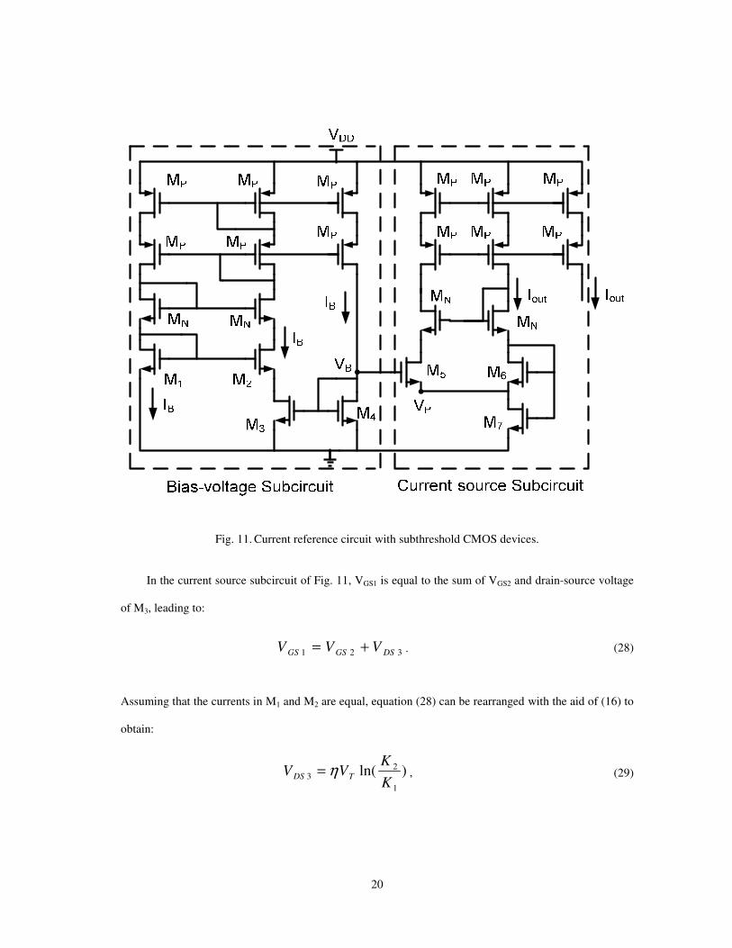
20
Fig. 11. Current reference circuit with subthreshold CMOS devices.
In the current source subcircuit of Fig. 11, VGS1 is equal to the sum of VGS2 and drain-source voltage
of M3, leading to:
321 DSGSGS VVV += . (28)
Assuming that the currents in M1 and M2 are equal, equation (28) can be rearranged with the aid of (16) to
obtain:
)ln(1
23
K
KVV TDS η= , (29)
21
where the K1 and K2 are the aspect ratios (= W/L) of M1 and M2. Since the MOS resistor M3 is biased in
the strong inversion, deep triode region; its resistance is given by
)(
1
3
3
THBox
MVVCK
R−
=µ
. (30)
The diode-connected transistor M4 operates in the strong inversion, saturation region. Thus, its drain
current IB can be expressed as
2
44 )(
2THB
oxB VV
CKI −=
µ. (31)
Since the bias current IB of M3 is equal to that of M4, VB becomes
)ln(2
1
2
4
34
K
KV
K
KVV TTHB η+= .
(32)
The current through M5 is mirrored to obtain the output current Iout. This current can be expressed as
)exp( 505
T
THPBout
V
VVVIKI
η
−−= ,
(33)
where VP is the source voltage of M5:
76
7
6
67
)2
ln( THT
GSGSP
VK
KV
VVV
δη −=
−=
. (34)
δVTH76 is the difference between the threshold voltages of M7 and M6. In order to bias transistor M5 in the
subthreshold region, the voltage VP has to be set to a large value by adjusting the sizes of M6 and M7. By
combining equations (32) to (34), the equation for the output current can be written as
22
4
32
1
2
6
750 )(
2)exp(
K
K
T
THout
K
K
K
KK
V
VII
η
δ= , (35)
where δVTH = VTH7 + VTH4 - VTH6 - VTH5, of which the value depends on the transistor dimensions. The
temperature dependence of the threshold voltage and the mobility can be expressed as
m
THTH
TTTT
TVV
−=
−=
)/)(()( 00
0
µµ
κ ,
(36)
where the µ(T0) is the carrier mobility at room temperature T0, m is the mobility temperature exponent,
VTH0 is the threshold voltage at 0K, and κ is the TC of VTH. By taking the derivative with respect to
temperature, the TC of the output current is derived as follows in [20]:
T
V
Vm
dT
V
Vd
V
VdT
dV
VdT
d
dT
dI
ITC
T
TH
T
TH
T
TH
T
T
out
out
)(2
)exp(
)exp(
111
1
0
0
02
η
δ
η
δ
η
δµ
µ
−−
=
++=
=
, (37)
where the δVTH0 = VTH07 + VTH04 - VTH06 - VTH05 at 0 K. Therefore, the zero TC condition for the output
current is
0)(2 0 =−−T
TH
V
Vm
η
δ.
(38)
In summary, this nano-ampere reference current generating technique is feasible for low-power
applications, but it has a drawback for the target application in this thesis. It can be observed from
23
equation (35) that the absolute value of the reference current is exponentially related to the threshold
voltage. Typically, the threshold voltage varies up to 20% in different process corner situations, which
would cause a large deviation of the reference current. In other words, the reference current generator
described above is not process insensitive enough.
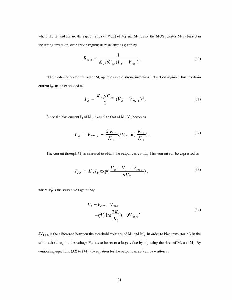
Fig. 12. Current reference circuit using subthreshold MOS resistor ladder.
Shown in Fig. 12 is the nano-ampere current reference circuit from [21], which uses a subthreshold
MOS resistor ladder. It consists of a bias-voltage section, a current source section, an offset voltage
generation block, and a start-up circuit (not shown). All transistors (except MR) are biased in the
subthreshold region, and transistors with the same name (MP) have the same dimensions. The MOS
resistor (MR) operates in strong-inversion and is biased in the deep triode region. This has the advantage
that the output current is more robust to process variations and mismatches than the design in [20].

24
The current Iref in Fig. 12 is determined by the characteristics of the strongly-inverted MOS resistor
MR biased in the deep triode region. When drain-source voltage VDSR is sufficiently small, than the current
is given by
DSRthgsoxnref VVVKCI )( −= µ , (39)
where Cox is the gate-oxide capacitance, Vth (= VTH0 – κT ) is the threshold voltage, VTH0 is the threshold
voltage at 0 Kelvin, κ is the temperature coefficient of the transistors’ threshold voltage, K is the aspect
ratio (W/L) of MR, and µn is the carrier mobility that can be modeled with a temperature dependence of
m
T
TT
−= )()(0
0µµ ; (40)
where µ0 is the mobility at room temperature T0, and m is the mobility temperature exponent. Assuming
that VDSR has an offset voltage (β) that is generated by an offset generation block, the temperature
dependence of VDSR can be expressed as:
βα += TV DSR , (41)
where α is the temperature coefficient of VDSR. From equations (39)-(41), the temperature coefficient TC1
of the reference current Iref was derived in [21]:
α
βT
1
T
m1
TTT
m
dT
dV
VdT
VVd
VVdT
dTC DSR
DSR
THGS
THGS
1
+
+−
=
+++
−=
+−
−+=
βα
α
µ
µ
1
1)(11
. (42)
25
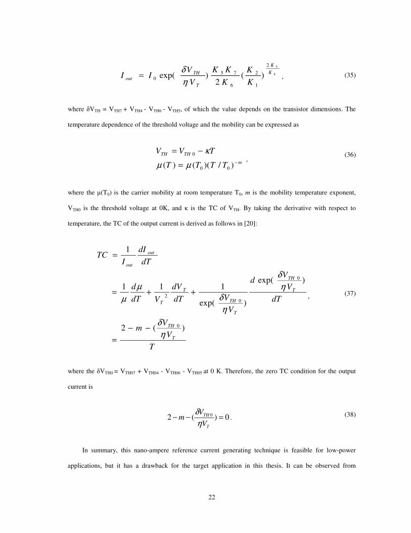
In standard CMOS technology, parameter m is approximately 1.5. Hence, TC1 can be forced to 0 at
room temperature by setting the β/α ratio to an appropriate value. Without an offset voltage (β = 0), TC1 is
always positive, but TC1 can be set to 0 at 300K when β/α = 300.
Fig. 13. Subthreshold MOS resistor ladder consisting of N MOSFETs.
Fig. 13 shows the offset voltage generation circuit reported in [21], which consists of several MOSFETs
connected in series. All the transistors are operating in the subthreshold linear region except the diode-
connected transistor M0 which operates in the subthreshold saturation region. Offset voltages can be
obtained from the voltages at each tap of the ladder. To simplify the analysis, the number of the transistors
is reduced to three as shown in Fig. 14.
26
Fig. 14. Subthreshold MOS resistor ladder consisting of 3×MOSFETs.
M0 in Fig. 14 operates in the subthreshold linear region, and M1 and M2 operate in the subthreshold
saturation region. The currents trough the transistors are
)exp( 1000
T
THDG
V
VVVIKI
η
−−= , (43)
))exp(1)(exp( 21201
T
DD
T
THDG
V
VV
V
VVVIKI
−−−
−−=
η, (44)
))exp(1)(exp( 202
T
D
T
THG
V
V
V
VVIKI −−
−=
η. (45)
The internal voltage VD2 can be expressed as
))ln(1()(
0
2
0
0
2
2I
KI
IKI
IVKIV T
D ++
=η
η. (46)
VD2 can be interpreted as a linear function with respect to the temperature, and equation (46) can be
simplified to [21]
βγ += TV D 2 . (47)
The temperature coefficient and the offset voltage in the above equation can be controlled by setting
appropriate number of the transistors and the tap point in the resistor ladder.
27
Fig. 15. Nano-ampere current reference proposed in [21].
Fig. 15 shows the schematic of the practical nano-ampere current reference from [21], where the
internal voltage VSR can be expressed as
βγ += TV SR . (48)
The drain-source voltage of MR is
βα
ηβγ
η
+=
++=
+=
−+=
T
K
KVT
K
KVV
VVVV
T
TSR
GSGSSRDSR
)ln(
)ln(
1
2
1
2
21
, (49)
where:
)ln(1
2
K
KV Tηγα += , (50)
K is the aspect ratio (=W/L) of a transistor, µ is the carrier mobility, COX is the gate-oxide capacitance, VT
(=kT/q) is the thermal voltage, k is the Boltzmann constant, T is the absolute temperature, q is the
elementary charge, VTH is the threshold voltage, and η is the subthreshold factor [18]. Based on the above
28
equations, the temperature coefficient of the reference current can be set to zero around room temperature
by adjusting γ and β with the taping point and the aspect ratios of the transistors in the ladder.
Table III. MOS ladder circuit characteristics [21]
Number of transistors Tap point γ (µV/K) β (mV)
10
5 63.6 4.3
6 84.6 5.66
1 112 7.49
8
155
10.5
9 7 145 9.81
11 7 93.3 6.28
Table III summarizes the characteristics of the internal voltages with various sets of transistors in the
configuration. The results show that we can control γ and β by deciding on the number of transistors and
picking the appropriate tap point. Unfortunately, the temperature compensation for the current (Iref) in Fig.
15 and the voltage (Vref) in Fig. 10 are independent of each other. The proposed method described in the
next subsection leads to a circuit that simultaneously generates a reference current and voltages that are
temperature-compensated.
2.3.2. Proposed temperature-independent current and voltage reference
Fig. 16. Proposed reference generation circuit.
29
Fig. 16 displays the proposed reference generation circuit, which utilizes the current generation
method described in [21] to produce a temperature-compensated reference current Iref. This reference
current is copied and forced to flow into the diode-connected transistor M8 to generate the reference
voltage Vmin. By design, Iref has a value that is sufficiently small to ensure that M8 is operating in the
subthreshold region, resulting in a subthreshold drain-source current equal to:
T
thgs
V
VV
M eIKIη
−
=
8
088 , (51)
where η is the subthreshold slope factor, I0 = µnCox (η-1)·(VT)2, VT = kBT/q is the thermal voltage, and the
equation implies that the drain-source voltage is larger than 0.1 V [17]. After equating (39) and (51), the
expression for Vgs8 can be obtained, which is equal to the reference voltage:
( )thVKC
VVVKC
Tgs VVVVToxn
dsRthgsRRoxn +==−
−
28 )1(
)(
8min lnηµ
µη .
Thus, the temperature coefficient of Vmin is:
))((
)1()()ln(
0
3
8
3
min
βακ
ηηη
++−
−−++=
∂
∂=
TTVVKq
KDCBk
q
Ak
T
VTC
THgsR
REF
, (52)
where:
22
8
2
0
)1(
))((
TkK
qTTVVKA
THgsR
−
++−=
η
βακ. (53)
22
8
2
)1(
)(
TkK
qTKB R
−
+=
η
βακ. (54)
22
8
2
0
)1(
)(
TkK
qTVVKC
THgsR
−
+−=
η
ακ. (55)

30
32
8
2
0
)1(
))((2
TkK
qTTVVKD
THgsR
−
++−=
η
βακ. (56)
The temperature coefficient of Vmin can be compensated around room temperature by selecting the
appropriate W/L ratio for M8. Due to the complexity of the equation, the proper W/L ratio was chosen
with a sweep during simulations. Notice that equation (52) still has temperature dependence, but this
dependence is reduced significantly due to the partial cancellation of the terms. Furthermore, the value of
Vmin is constrained by the requirements to achieve a near-zero temperature coefficient with the given
design parameters and process technology based on equation (52). On the hand, the value of Vmax in Fig.
16 is generated with a ratioed resistor ladder, such that a different value of Vmax can be generated by
adopting a different resistance ratio. In this design, the value of Vmax was selected based on the common-
mode input range of the comparator and the desired oscillation frequency according to equation (2).
Fig. 16 also shows the output stage configuration with which we can generate the required reference
voltage and reference current for the oscillator. The output Iref = 26.84nA is copied by a 1:4 current mirror
(transistors M9 - M12), such that the final output currents are: IrefP = IrefN = 118nA. The two reference
voltages Vmin and Vmax are 484.6mV and 663.5mV at room temperature, where Vmax is generated from a
ladder with high-resistance polysilicon resistors. In order to minimize the effects of process variations, the
resistor ladder is composed of 30 segments of 25KΩ high-resistance polysilicon resistors, and a common-
centroid layout technique was used.
2.4. Comparator design
The relaxation oscillator architecture in Fig. 6 contains two comparators. In general, a comparator is
defined as a device that has a binary output whose value is based on the comparison of two analog inputs.
Basically, the comparator is a 1-bit ADC with the ideal transfer function shown in Fig. 17, where the
output is equal to VOH when Vin+ - Vin- > 0 and equal to VOL when Vin+ − Vin- < 0. An ideal comparator has
infinite gain, zero offset voltage and zero root-mean-square (RMS) noise.

31
Fig. 17. Ideal comparator transfer function.
In a practical situation, the comparator has a finite gain and is affected by the non-zero offset and
RMS noise, for which the impact on the relative transfer function is visualized in Fig. 18 with
exaggeration. The non-ideal gain can be defined as
ILIH
OLOHv
VV
VVA
−
−= , (57)
where VIH - VIL represents the input voltage difference that is required to saturate the comparator output at
its upper (VOH) and lower limit (VOL). Hence, This VIH - VIL indicates the resolution of the comparator.
Fig. 18. Non-ideal comparator transfer function.
Another non-ideality is the input-referred offset voltage, labeled VOS in Fig. 18, which could be
positive or negative. This offset voltage varies randomly from chip to chip due to mismatches caused by
fabrication process variations. Comparator offset is a concern for the relaxation oscillator design in Fig. 6

32
because the offset voltage directly impacts the oscillation frequency determined by equation (2). For
instance, assuming that Vmax - Vmin = 200mV and an input-referred offset of ±10mV, the variation of the
frequency would be 10%.
2.4.1. Open-loop comparator
The open-loop comparator in Fig. 19 [22] is a single-stage amplifier without compensation to obtain
a fast response time. Stability is not a concern because the amplifier is used without feedback from its
output to its input. Nevertheless, the transistor dimensions should be carefully selected to minimize the
effect of parasitic capacitances in order to minimize the response time.
Fig. 19. Open-loop comparator.
The amplifier in Fig. 19 was designed for the application in the relaxation oscillator of Fig. 6.
Transistors M1 and M2 in Fig. 19 have the same dimensions, and equal-sized transistors M3 and M4 form a
1:1 current mirror. The amplifier’s gain can be expressed as
)(42
421
oo
oo
mvrr
rrgA
+= , (58)
where the gmX and roX are the transconductance and output resistance of the corresponding transistor MX.
33
The comparator has one dominant pole frequency (ωp) of interest, which is created at the output. This
pole in the frequency response can be approximated as
)(
1
42
421
oo
oo
p
rr
rrC
+
=ω , (59)
dX
oXI
rλ
1≈ ;
(60)
where the C1 represent the sum of the capacitances connected to nodes VP in Fig. 19, and IdX is the drain-
source current of transistor MX. The frequency response of the comparator can be estimated as
p
v
s
AsA
ω+
=
1
)( , (61)
From the above equations, it can be observed that the bandwidth of the comparator is strongly
affected by the parasitic capacitances and drain-source resistances, as well as the transconductance that
determines the voltage gain. Since a high transconductance value requires a large bias current, there is a
trade-off between power consumption and speed. However, the oscillator design presented in this thesis is
intended for target frequencies below 100KHz, allowing to design with low power consumption by
sacrificing speed. The components dimensions used in the open-loop comparator design (Fig. 19) are
listed in Table IV.
Table IV. Dimensions of the devices in the comparator
Component Name
(in Fig. 19) Dimensions [(width/length)×segments] or Value
M1 (800nm / 1µm) × 2
M2 (800nm / 1µm) × 2
M3 (500nm / 4.5µm) × 2
M4 (500nm / 4.5µm) × 2
M5 (1.6µm / 1µm) × 2
C1 200fF
34
2.5. Switch design
Two conventional transmission gates are used to control the charging and discharging the capacitor
CT in Fig. 6. In comparison to employing a single transistor for each switch, the use of transmission gates
has the benefit that the on-resistance is lower and less dependent on the voltages on the terminals
connected to CT and the reference current source. The additional parasitic capacitances from the second
transistor are not critical in this low-frequency application.
2.6. SR latch design
A latch is a circuit that has two stable states and can be used to store state information. The relaxation
oscillator in Fig. 6 uses a basic SR latch, where “S” and “R” stand for Set and Reset. Such a latch can be
constructed from a pair of cross-coupled NOR logic gates as shown in Fig. 20, where the stored bit is
present at the output marked Q.
Fig. 20. A SR latch constructed from a pair of cross-coupled NOR gates.
35
Fig. 21. Schematic of the SR latch in the relaxation oscillator.
When the S and R inputs in Fig. 20 are both low, the feedback keeps the Q and Qbar outputs in a
constant state, where Qbar is the complement of Q. If S (Set) is pulsed high while R (Reset) is held low,
then the Q output is forced high, and stays high when S returns to low. Similarly, if R is pulsed high while
S is held low, then the Q output is forced low, and stays low when R returns to low. The Q and Qbar
outputs are supposed to be in opposite states. When both the S and R inputs are equal to 1, then both Q and
Qbar become 0. For this reason, having both S and R equal to 1 is considered an invalid or illegal state for
the SR latch. Otherwise, applying inputs of S = 1 and R = 0 "sets" the latch such that Q = 1 and Qbar = 0.
Conversely, applying R = 1 and S = 0 "resets" the latch in the opposite state (Q = 0, Qbar = 1). When S and
R are both equal to 0, the latch's outputs "latch" into their prior states. The truth table that summarizes the
SR latch operation is provided in Table V. In this application, the sizes of PMOS and NMOS transistors

36
should be properly scaled to keep the trip point of the latch equal to VDD/2. Fig. 21 shows the schematic of
the SR latch designed for the relaxation oscillator, and the corresponding transistor dimensions are listed
in Table VI.
Table V. Truth table of the SR latch
S R Q Qbar
0 0 Latch Latch
0 1 0 1
1 0 1 0
1
1
Invalid Invalid
Table VI. Dimensions of the devices in the SR latch
Component Name
(in Fig. 21) Dimensions [(width/length)×segments] or Value
M1 (500nm / 500nm) × 2
M2 (500nm / 500nm) × 2
M3 (2.1µm / 500nm) × 2
M4 (2.1µm / 500nm) × 2
M5 (500nm / 500nm) × 2
M6 (500nm / 500nm) × 2
M7 (2.1µm / 500nm) × 2
M8 (2.1µm / 500nm) × 2

37
3. SIMULATION RESULTS
3.1. Reference generator simulation results
The performance of the design in Dongbu 0.11µm CMOS technology was assessed with Cadence
Spectre simulations. The relaxation oscillator in Fig. 6 operates with a supply voltage of 1.2V, and
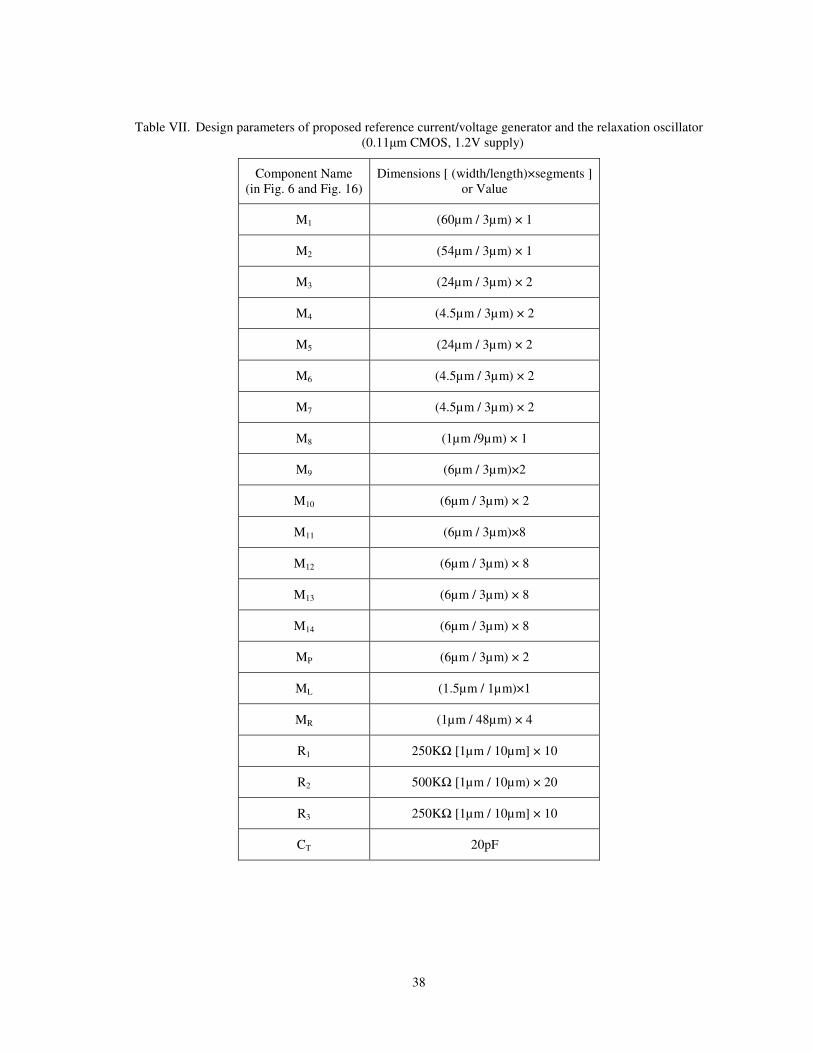
consumes a total power of 4.9µW. Table VII lists the most relevant dimensions and values of components.
It can be observed from the table that large dimensions and multipliers are selected to allow the use of the
common-centroid layout technique to make the performance more robust to process variations and
mismatches.
Fig. 22 shows the reference current as a function of temperature. From the figure it can be observed
that the current varies very little around the temperature compensation point of 25ºC. The temperature
coefficient is 166ppm/ºC over a range from -20ºC to 80ºC. Fig. 23 displays the temperature dependence of
the reference voltage Vmax. The reference voltage is 663.5mV at room temperature and has a temperature
coefficient of 7.5ppm/ºC over a range from -20ºC to 80ºC. Fig. 24 reveals how reference voltage Vmin
varies with temperature. The generated reference voltage is 484.6mV at room temperature with a
temperature coefficient of 16ppm/ºC over the -20ºC to 80ºC range.
38
Table VII. Design parameters of proposed reference current/voltage generator and the relaxation oscillator
(0.11µm CMOS, 1.2V supply)
Component Name
(in Fig. 6 and Fig. 16)
Dimensions [ (width/length)×segments ]
or Value
M1 (60µm / 3µm) × 1
M2 (54µm / 3µm) × 1
M3 (24µm / 3µm) × 2
M4 (4.5µm / 3µm) × 2
M5 (24µm / 3µm) × 2
M6 (4.5µm / 3µm) × 2
M7 (4.5µm / 3µm) × 2
M8 (1µm /9µm) × 1
M9 (6µm / 3µm)×2
M10 (6µm / 3µm) × 2
M11 (6µm / 3µm)×8
M12 (6µm / 3µm) × 8
M13 (6µm / 3µm) × 8
M14 (6µm / 3µm) × 8
MP (6µm / 3µm) × 2
ML (1.5µm / 1µm)×1
MR (1µm / 48µm) × 4
R1 250KΩ [1µm / 10µm] × 10
R2 500KΩ [1µm / 10µm) × 20
R3 250KΩ [1µm / 10µm] × 10
CT 20pF

39
Fig. 22. Simulated reference current (Iref in Fig. 16) vs. temperature.
Fig. 23. Simulated reference voltage Vmax vs. temperature.

40
Fig. 24. Simulated reference voltage Vmin vs. temperature.
Fig. 25 and Fig. 26 visualize the distributions of Vmin and Vmax obtained from 100 Monte Carlo
simulations with foundry-supplied device models. The standard deviations (σ) are 1.023mV and 0.767mV,
resulting in very low variations as evident after normalization with the mean values (µ): σ/µ is 0.2% for
Vmin and 0.11% for Vmax. Fig. 27, Fig. 28 and Fig. 29 display the distributions of Iref obtained from 100
Monte Carlo simulations at 27ºC, -20ºC, and 80ºC, respectively. In all cases, the standard deviation of Iref
is less than 6% of its mean value. The Monte Carlo simulation results suggest that the reference current is
robust to device mismatches, which leads to reliable currents IrefP and IrefN because they are copied from Iref
using current mirrors with a multiplication factor of 4.
41
Fig. 25. Histogram of Vmin obtained from 100 Monte Carlo simulations.
Fig. 26. Histogram of Vmax obtained from 100 Monte Carlo simulations.
42
Fig. 27. Histogram of Iref after 100 Monte Carlo simulations at 27 ºC.
Fig. 28. Histogram of the Iref after 100 Monte Carlo simulations at -20 ºC.
43
Fig. 29. Histogram of the Iref after 100 Monte Carlo simulations at 80 ºC.
Table VIII. Simulated reference generator output values for different process corners at room temperature
Process Corner Vmax Vmin Iref
TT 484.6mV 663.5mV 26.84nA
FF 438mV 628mV 27.81nA
SS 533mV 699mV 25.82nA
Table VIII. summarizes the simulated values of the reference voltages and reference current for
different process corner cases. The results indicate that reference current is robust to the process variations.
On the other hand, the absolute value of the reference voltage varies significantly. However, the difference
between the two reference voltages changes only ±11mV, which leads to a robust oscillation frequency as
dictated by equation (2) based on this voltage difference. The correlation of the reference voltages stems
from the fact that Vmax is generated from Vmin using a resistive divider as shown in Fig. 16. Hence, it is
important that resistors R1, R2 and R3 are matched in the layout such that the correlation between Vmin and
Vmax that reduces the variation of the difference (Vmax - Vmin) depends on the following equation:

44
min
321
3
321
3max )1(
)(V
RRR
R
RRR
RVV DD
++−+
++= . (62)
Table IX. Comparison with other reference generation circuits
This work+ [23]
++ [17]
++ [21]
+ [24]
++
Process 0.11µm 0.18µm 0.35µm 0.35µm 3µm
VDD 1.2V 1.5V 1.4-3V 2.5V 5V
Power
Consumption 1µW 17.25µW 300nW 0.81µW 10µW
Output Reference
Voltage
484.6 mV
663.5 mV 621mV 745mV N/A N/A
Output Reference
Current 26.84nA N/A N/A 92.7nA 774nA
TC of The
Output Voltage
7.5ppm/ºC
(663.5mV)
16ppm/ºC
(484.6mV)
11.5ppm/ºC 7ppm/ºC N/A N/A
TC of the Output
Current 166ppm/ºC N/A N/A 288ppm/ºC 375ppm/ºC*
Temperature
Range -20 - 80ºC -20 - 120ºC -20 - 80ºC -20 - 100ºC 0 - 80ºC
* The temperature dependence was reported as 3% from 0ºC to 80ºC. +
Simulation result. ++
Measurement result.
Table IX compares the performance of the integrated reference generator with other reference
circuits. The proposed reference generator can generate two different output voltages and a nano-ampere
range current simultaneously, which is a feature that the other reference generation circuits do not have. In
comparison, the dual reference voltage/current generation circuit from this work has relatively low
temperature coefficients and low power consumption, making it suitable for low-power applications.
45
3.2. Comparator simulation results
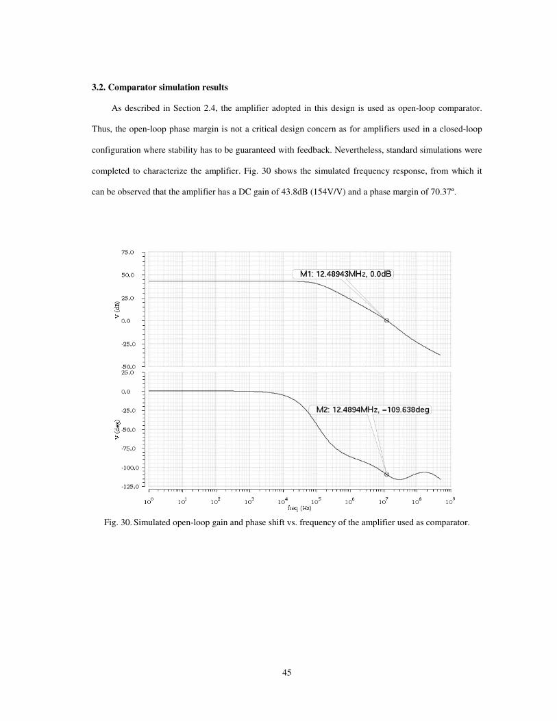
As described in Section 2.4, the amplifier adopted in this design is used as open-loop comparator.
Thus, the open-loop phase margin is not a critical design concern as for amplifiers used in a closed-loop
configuration where stability has to be guaranteed with feedback. Nevertheless, standard simulations were
completed to characterize the amplifier. Fig. 30 shows the simulated frequency response, from which it
can be observed that the amplifier has a DC gain of 43.8dB (154V/V) and a phase margin of 70.37º.
Fig. 30. Simulated open-loop gain and phase shift vs. frequency of the amplifier used as comparator.
46
Fig. 31. Histogram of the comparator’s input-referred offset voltage obtained with 100 Monte Carlo
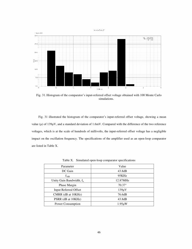
simulations.
Fig. 31 illustrated the histogram of the comparator’s input-referred offset voltage, showing a mean
value (µ) of 139µV, and a standard deviation of 1.6mV. Compared with the difference of the two reference
voltages, which is at the scale of hundreds of millivolts, the input-referred offset voltage has a negligible
impact on the oscillation frequency. The specifications of the amplifier used as an open-loop comparator
are listed in Table X.
Table X. Simulated open-loop comparator specifications
Parameter Value
DC Gain 43.8dB
f3dB 95KHz
Unity Gain Bandwidth, fu 12.87MHz
Phase Margin 70.37°
Input Referred Offset 139µV
CMRR (dB at 10KHz) 76.6dB
PSRR (dB at 10KHz) 43.8dB
Power Consumption 1.95µW
47
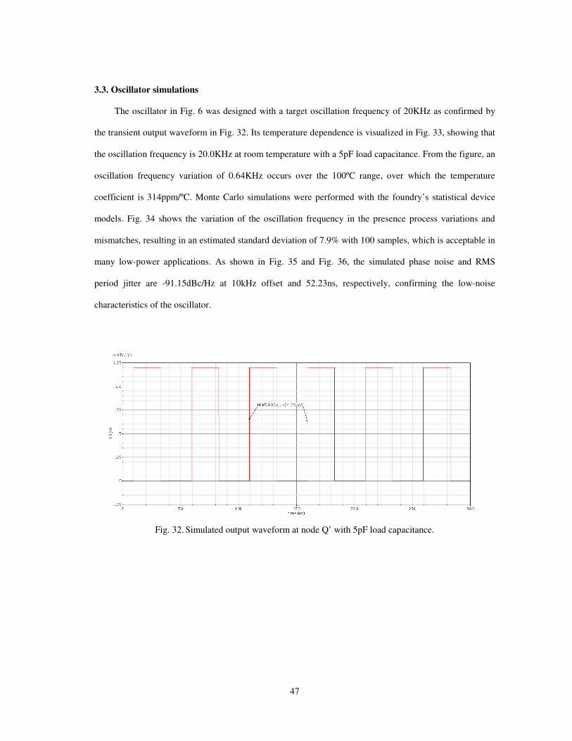
3.3. Oscillator simulations
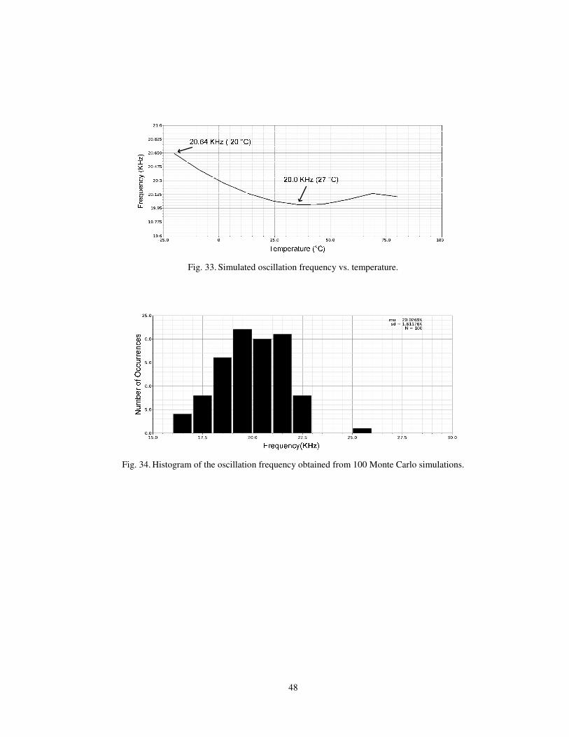
The oscillator in Fig. 6 was designed with a target oscillation frequency of 20KHz as confirmed by
the transient output waveform in Fig. 32. Its temperature dependence is visualized in Fig. 33, showing that
the oscillation frequency is 20.0KHz at room temperature with a 5pF load capacitance. From the figure, an
oscillation frequency variation of 0.64KHz occurs over the 100ºC range, over which the temperature
coefficient is 314ppm/ºC. Monte Carlo simulations were performed with the foundry’s statistical device
models. Fig. 34 shows the variation of the oscillation frequency in the presence process variations and
mismatches, resulting in an estimated standard deviation of 7.9% with 100 samples, which is acceptable in
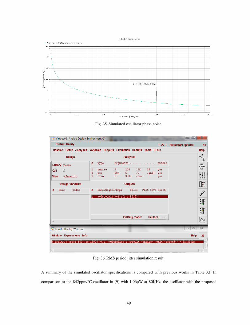
many low-power applications. As shown in Fig. 35 and Fig. 36, the simulated phase noise and RMS
period jitter are -91.15dBc/Hz at 10kHz offset and 52.23ns, respectively, confirming the low-noise
characteristics of the oscillator.
Fig. 32. Simulated output waveform at node Q’ with 5pF load capacitance.
48
Fig. 33. Simulated oscillation frequency vs. temperature.
Fig. 34. Histogram of the oscillation frequency obtained from 100 Monte Carlo simulations.
49
Fig. 35. Simulated oscillator phase noise.
Fig. 36. RMS period jitter simulation result.
A summary of the simulated oscillator specifications is compared with previous works in Table XI. In
comparison to the 842ppm/°C oscillator in [9] with 1.06µW at 80KHz, the oscillator with the proposed
50
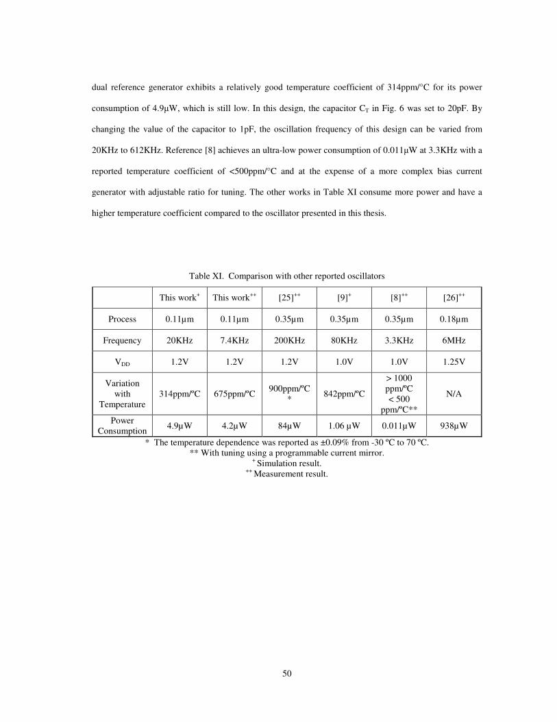
dual reference generator exhibits a relatively good temperature coefficient of 314ppm/°C for its power
consumption of 4.9µW, which is still low. In this design, the capacitor CT in Fig. 6 was set to 20pF. By
changing the value of the capacitor to 1pF, the oscillation frequency of this design can be varied from
20KHz to 612KHz. Reference [8] achieves an ultra-low power consumption of 0.011µW at 3.3KHz with a
reported temperature coefficient of <500ppm/°C and at the expense of a more complex bias current
generator with adjustable ratio for tuning. The other works in Table XI consume more power and have a
higher temperature coefficient compared to the oscillator presented in this thesis.
Table XI. Comparison with other reported oscillators
This work+ This work
++ [25]
++ [9]
+ [8]
++ [26]
++
Process 0.11µm 0.11µm 0.35µm 0.35µm 0.35µm 0.18µm
Frequency 20KHz 7.4KHz 200KHz 80KHz 3.3KHz 6MHz
VDD 1.2V 1.2V 1.2V 1.0V 1.0V 1.25V
Variation
with
Temperature
314ppm/ºC 675ppm/ºC 900ppm/ºC
* 842ppm/ºC
> 1000
ppm/ºC
< 500
ppm/ºC**
N/A
Power
Consumption 4.9µW 4.2µW 84µW 1.06 µW 0.011µW 938µW
* The temperature dependence was reported as ±0.09% from -30 ºC to 70 ºC.
** With tuning using a programmable current mirror. +
Simulation result. ++
Measurement result.
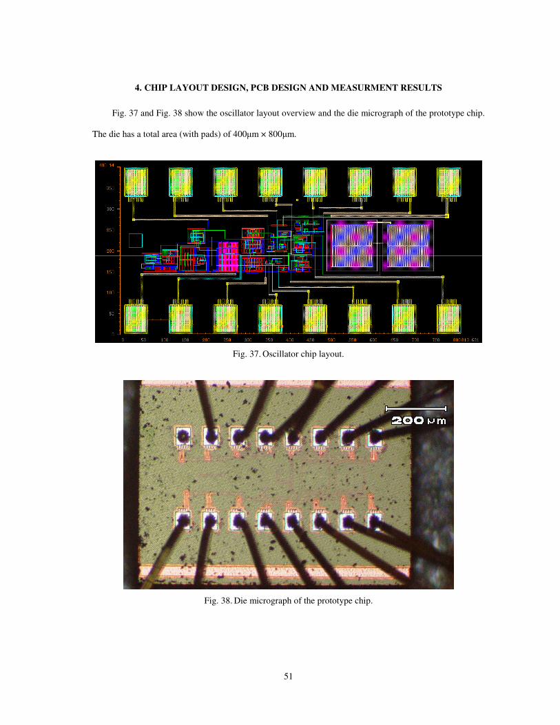
51
4. CHIP LAYOUT DESIGN, PCB DESIGN AND MEASURMENT RESULTS
Fig. 37 and Fig. 38 show the oscillator layout overview and the die micrograph of the prototype chip.
The die has a total area (with pads) of 400µm × 800µm.
Fig. 37. Oscillator chip layout.
Fig. 38. Die micrograph of the prototype chip.
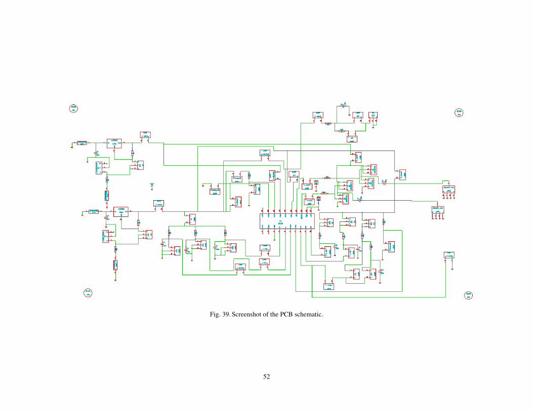
52
Fig. 39. Screenshot of the PCB schematic.
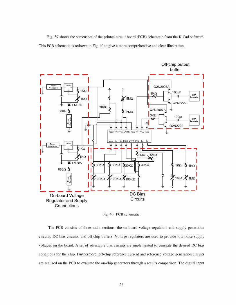
53
Fig. 39 shows the screenshot of the printed circuit board (PCB) schematic from the KiCad software.
This PCB schematic is redrawn in Fig. 40 to give a more comprehensive and clear illustration.
VSS1 VH VL Start CTR1 INE IB1IB2
VSS2QbarQVDD2OUTEVDD1CTR2VDD3
SMA
Connector
SMA
Connector
Power
Connector
Power
Connector
LM350
In Out
ADJ
LM385
680Ω
1KΩ
1KΩ
Power
Connector
Power
Connector
LM350
In Out
ADJ
LM385
680Ω
1KΩ
1KΩ
30KΩ
100KΩ
2MΩ 5MΩ
1MΩ
1KΩ
3KΩ
3KΩ
Q2N2222
Q2N2907A
100μF
5MΩ
2MΩ
30KΩ
Off-chip output
buffer
DC Bias
CircuitsOn-board Voltage
Regulator and Supply
Connections
30KΩ
100KΩ
30KΩ
100KΩ
30KΩ
1MΩ
1KΩ
Q2N2907A
Q2N2222
100μF
Fig. 40. PCB schematic.
The PCB consists of three main sections: the on-board voltage regulators and supply generation
circuits, DC bias circuits, and off-chip buffers. Voltage regulators are used to provide low-noise supply
voltages on the board. A set of adjustable bias circuits are implemented to generate the desired DC bias
conditions for the chip. Furthermore, off-chip reference current and reference voltage generation circuits
are realized on the PCB to evaluate the on-chip generators through a results comparison. The digital input
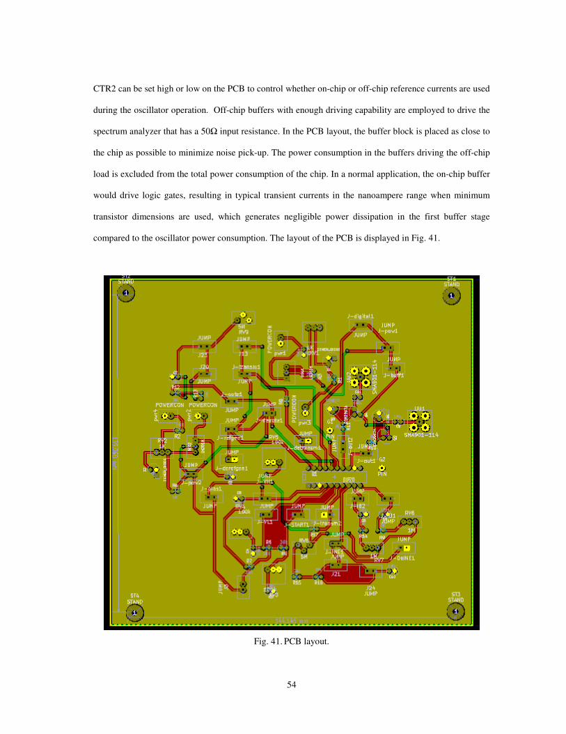
54
CTR2 can be set high or low on the PCB to control whether on-chip or off-chip reference currents are used
during the oscillator operation. Off-chip buffers with enough driving capability are employed to drive the
spectrum analyzer that has a 50Ω input resistance. In the PCB layout, the buffer block is placed as close to
the chip as possible to minimize noise pick-up. The power consumption in the buffers driving the off-chip
load is excluded from the total power consumption of the chip. In a normal application, the on-chip buffer
would drive logic gates, resulting in typical transient currents in the nanoampere range when minimum
transistor dimensions are used, which generates negligible power dissipation in the first buffer stage
compared to the oscillator power consumption. The layout of the PCB is displayed in Fig. 41.
Fig. 41. PCB layout.
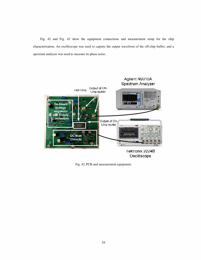
55
Fig. 42 and Fig. 43 show the equipment connections and measurement setup for the chip
characterization. An oscilloscope was used to capture the output waveform of the off-chip buffer, and a
spectrum analyzer was used to measure its phase noise.
Fig. 42. PCB and measurement equipment.
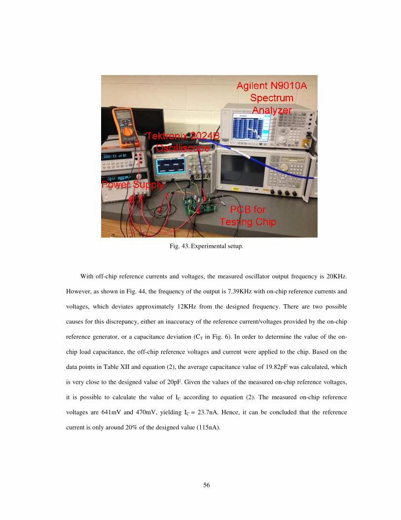
56
Fig. 43. Experimental setup.
With off-chip reference currents and voltages, the measured oscillator output frequency is 20KHz.
However, as shown in Fig. 44, the frequency of the output is 7.39KHz with on-chip reference currents and
voltages, which deviates approximately 12KHz from the designed frequency. There are two possible
causes for this discrepancy, either an inaccuracy of the reference current/voltages provided by the on-chip
reference generator, or a capacitance deviation (CT in Fig. 6). In order to determine the value of the on-
chip load capacitance, the off-chip reference voltages and current were applied to the chip. Based on the
data points in Table XII and equation (2), the average capacitance value of 19.82pF was calculated, which
is very close to the designed value of 20pF. Given the values of the measured on-chip reference voltages,
it is possible to calculate the value of IC according to equation (2). The measured on-chip reference
voltages are 641mV and 470mV, yielding IC = 23.7nA. Hence, it can be concluded that the reference
current is only around 20% of the designed value (115nA).
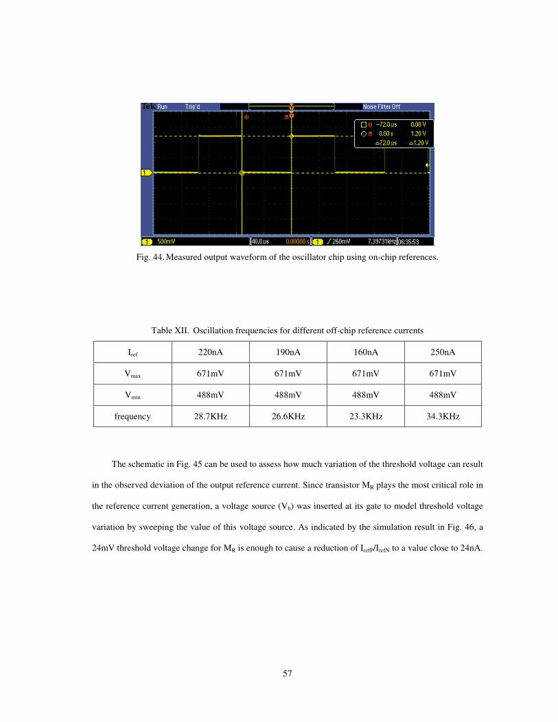
57
Fig. 44. Measured output waveform of the oscillator chip using on-chip references.
Table XII. Oscillation frequencies for different off-chip reference currents
Iref 220nA 190nA 160nA 250nA
Vmax 671mV 671mV 671mV 671mV
Vmin 488mV 488mV 488mV 488mV
frequency 28.7KHz 26.6KHz 23.3KHz 34.3KHz
The schematic in Fig. 45 can be used to assess how much variation of the threshold voltage can result
in the observed deviation of the output reference current. Since transistor MR plays the most critical role in
the reference current generation, a voltage source (Vb) was inserted at its gate to model threshold voltage
variation by sweeping the value of this voltage source. As indicated by the simulation result in Fig. 46, a
24mV threshold voltage change for MR is enough to cause a reduction of IrefP/IrefN to a value close to 24nA.
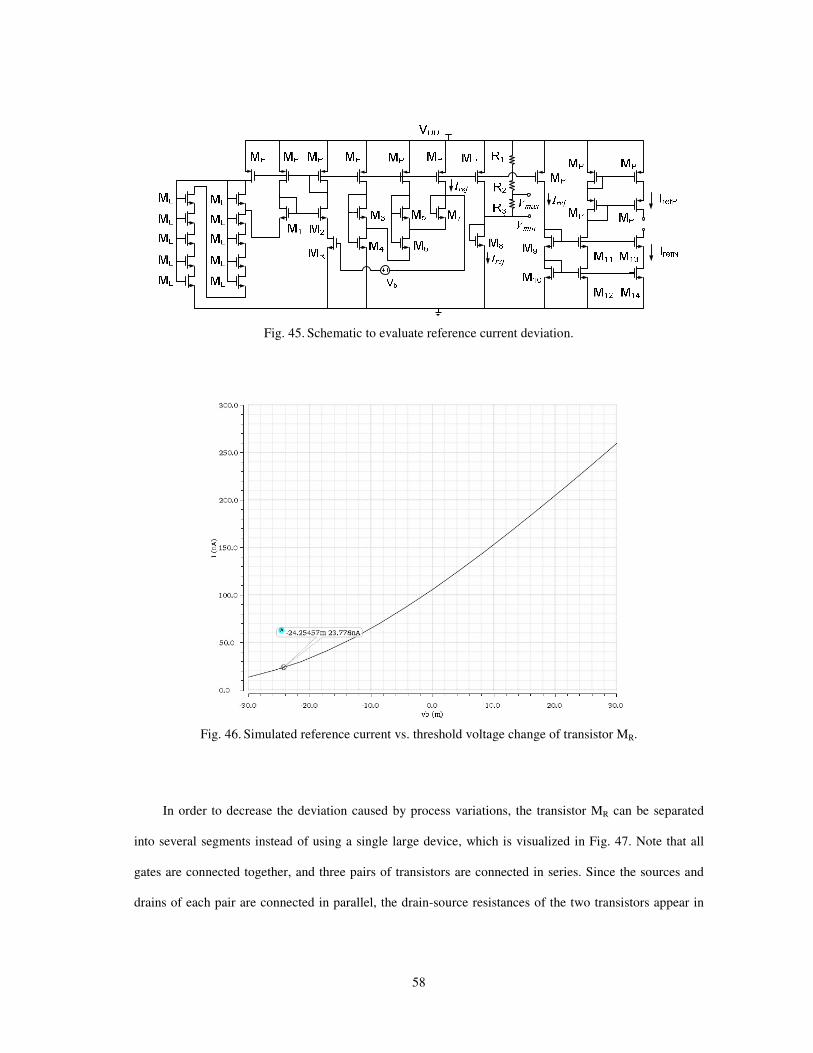
58
Fig. 45. Schematic to evaluate reference current deviation.
Fig. 46. Simulated reference current vs. threshold voltage change of transistor MR.
In order to decrease the deviation caused by process variations, the transistor MR can be separated
into several segments instead of using a single large device, which is visualized in Fig. 47. Note that all
gates are connected together, and three pairs of transistors are connected in series. Since the sources and
drains of each pair are connected in parallel, the drain-source resistances of the two transistors appear in

59
parallel. In this example, the transistor MR (width of 1µm, length of 48µm) was split into six equal-sized
transistors MR’ (width of 0.3µm, length of 10.5µm) such that the simulated resistances of both
configurations are identical. By implementing multipliers, the transistors can be matched in the layout to
reduce the impact of process variations. Monte Carlo simulations were performed to confirm the
improvement of the robustness to process variations. The corresponding result is shown in Fig. 48.
Fig. 47. Replacing MR with components with multiplier.
Fig. 48. Histogram of the Iref obtained with 100 Monte Carlo simulations after replacing MR with multiple
devices.
Fig. 48 shows the distribution of Iref after 100 Monte Carlo simulations, where the standard deviation
is 3.5%, which is an improvement compared to the 6% case in Section 3.1. More reduction of the standard
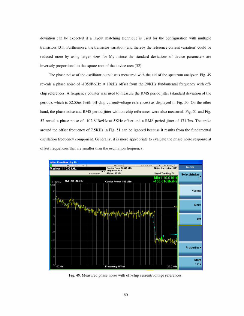
60
deviation can be expected if a layout matching technique is used for the configuration with multiple
transistors [31]. Furthermore, the transistor variation (and thereby the reference current variation) could be
reduced more by using larger sizes for MR’, since the standard deviations of device parameters are
inversely proportional to the square root of the device area [32].
The phase noise of the oscillator output was measured with the aid of the spectrum analyzer. Fig. 49
reveals a phase noise of -105dBc/Hz at 10kHz offset from the 20KHz fundamental frequency with off-
chip references. A frequency counter was used to measure the RMS period jitter (standard deviation of the
period), which is 52.55ns (with off-chip current/voltage references) as displayed in Fig. 50. On the other
hand, the phase noise and RMS period jitter with on-chip references were also measured. Fig. 51 and Fig.
52 reveal a phase noise of -102.8dBc/Hz at 5KHz offset and a RMS period jitter of 171.7ns. The spike
around the offset frequency of 7.5KHz in Fig. 51 can be ignored because it results from the fundamental
oscillation frequency component. Generally, it is more appropriate to evaluate the phase noise response at
offset frequencies that are smaller than the oscillation frequency.
Fig. 49. Measured phase noise with off-chip current/voltage references.
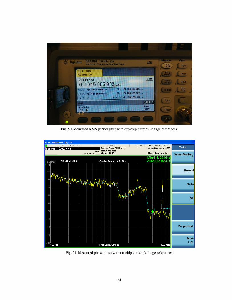
61
Fig. 50. Measured RMS period jitter with off-chip current/voltage references.
Fig. 51. Measured phase noise with on-chip current/voltage references.
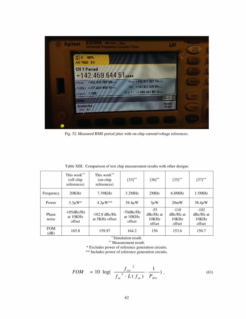
62
Fig. 52. Measured RMS period jitter with on-chip current/voltage references.
Table XIII. Comparison of test chip measurement results with other designs
This work++
(off-chip
references)
This work++
(on-chip
references)
[33]++
[36]++
[35]++
[37]++
Frequency 20KHz 7.39KHz 3.2MHz 2MHz 6.8MHz 1.5MHz
Power 3.3µW* 4.2µW** 38.4µW 3µW 20mW 38.4µW
Phase
noise
-105dBc/Hz
at 10KHz
offset
-102.8 dBc/Hz
at 5KHz offset
-70dBc/Hz
at 10KHz
offset
-55
dBc/Hz at
10KHz
offset
-110
dBc/Hz at
10KHz
offset
-102
dBc/Hz at
10KHz
offset
FOM
(dB) 165.8 159.97 164.2 156 153.6 150.7
+ Simulation result.
++ Measurement result.
* Excludes power of reference generation circuits.
** Includes power of reference generation circuits.
)1
)(log(10
2
2
dissmm
osc
PfLf
fFOM ⋅
⋅= , (63)
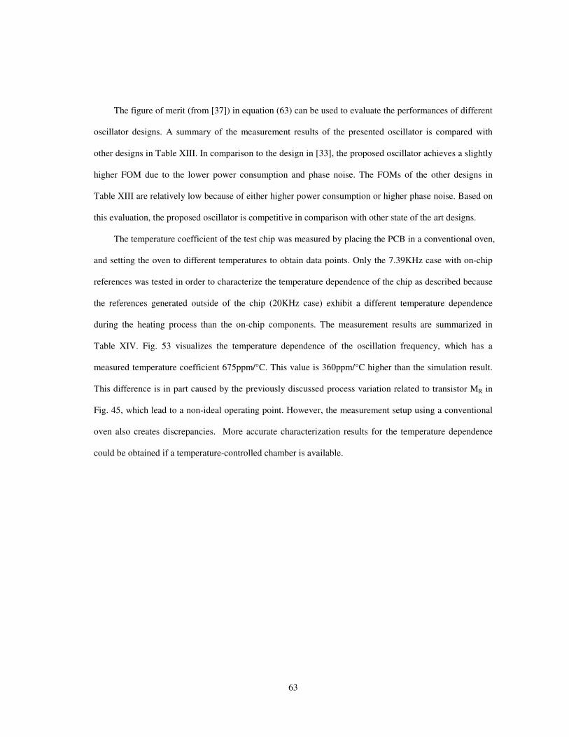
63
The figure of merit (from [37]) in equation (63) can be used to evaluate the performances of different
oscillator designs. A summary of the measurement results of the presented oscillator is compared with
other designs in Table XIII. In comparison to the design in [33], the proposed oscillator achieves a slightly
higher FOM due to the lower power consumption and phase noise. The FOMs of the other designs in
Table XIII are relatively low because of either higher power consumption or higher phase noise. Based on
this evaluation, the proposed oscillator is competitive in comparison with other state of the art designs.
The temperature coefficient of the test chip was measured by placing the PCB in a conventional oven,
and setting the oven to different temperatures to obtain data points. Only the 7.39KHz case with on-chip
references was tested in order to characterize the temperature dependence of the chip as described because
the references generated outside of the chip (20KHz case) exhibit a different temperature dependence
during the heating process than the on-chip components. The measurement results are summarized in
Table XIV. Fig. 53 visualizes the temperature dependence of the oscillation frequency, which has a
measured temperature coefficient 675ppm/°C. This value is 360ppm/°C higher than the simulation result.
This difference is in part caused by the previously discussed process variation related to transistor MR in
Fig. 45, which lead to a non-ideal operating point. However, the measurement setup using a conventional
oven also creates discrepancies. More accurate characterization results for the temperature dependence
could be obtained if a temperature-controlled chamber is available.
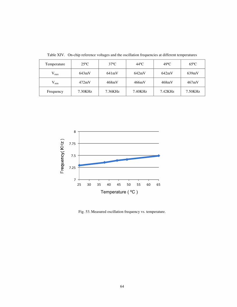
64
Table XIV. On-chip reference voltages and the oscillation frequencies at different temperatures
Temperature 25ºC 37ºC 44ºC 49ºC 65ºC
Vmax 643mV 641mV 642mV 642mV 639mV
Vmin 472mV 468mV 466mV 468mV 467mV
Frequency 7.30KHz 7.36KHz 7.40KHz 7.42KHz 7.50KHz
7
7.25
7.5
7.75
8
25 30 35 40 45 50 55 60 65
Frequency (KHz)
Frequency (KHz)
Temperature ( ºC )
Fig. 53. Measured oscillation frequency vs. temperature.
65
5. CONCLUSIONS AND FUTURE WORK
5.1. Conclusion
Several design considerations for low-power oscillators were discussed in this thesis. A circuit that
combines the generation of the reference currents and voltages for a relaxation oscillator was proposed and
analyzed. This circuit was employed during the design of a temperature-compensated relaxation oscillator
with low power consumption. In the presented design, the two output reference voltages are 484.6mV and
663.5mV, which have simulated temperature coefficients of 7.5ppm/ºC and 16ppm/ºC respectively. The
output reference current is 26.84nA, which has with a temperature coefficient of 166ppm/ºC. The total
power consumption of the relaxation oscillator is 4.9µW with a 1.2V supply in 0.11µm CMOS technology.
A prototype chip was fabricated in Dongbu 0.11µm CMOS technology to demonstrate the feasibility of
the design technique. The relaxation oscillator has a measured power consumption of 4.2µW, a
temperature coefficient of 675ppm/ºC, a phase noise of -102.8dBc/Hz at5 KHz offset with on-chip
references, and a phase noise of -105dBc/Hz at 10KHz offset with off-chip references.
5.2. Future work
As described in Chapter 4, the on-chip reference current value of the fabricated chip was
approximately 20% of the value specified during the design process, leading to a significant deviation of
the oscillation frequency. To counteract the effect of the process variation that caused the difference, an
on-chip self-calibration method could be developed. The implementation of this method could potentially
solve the reference current variation challenge. On the other hand, a re-design in which transistor MR
occupies a larger die area and has dimensions that allow to employ layout matching techniques can also
result in significant improvement of the reference current accuracy after fabrication.
66
REFERENCES
[1] C. Hwang, S. Bibyk, M. Ismail, and B. Lohiser, "A very low, micro power, low voltage CMOS
oscillator for noncardiac pacemaker," IEEE Trans. Circuits And Systems I: Fundamental Theory And
Applications, vol. 42, No.11, pp.962-966, Nov. 1995.
[2] R. Walters, G. Bivins, "A custom CMOS IC for pacemaker applications," in IEEE Intl. Solid-State
Circuits Conf. (ISSCC) Dig. Tech. Papers, Feb. 1979, pp. 200-201.
[3] L.S.Y. Wong, S. Hossain, A. Ta, J. Edvinsson, D.H. Rivas, H. Naas, " A very low-power CMOS
mixed-signal IC for implantable pacemaker applications," IEEE J. Solid-State Circuits, vol. 39, no. 12,
pp. 2446–2456, Dec. 2004.
[4] P. Sunghyun, M. Changwook, C. SeongHwan, "A 95nW ring oscillator-based temperature sensor for
RFID tags in 0.13µm CMOS," in Proc. IEEE Intl. Symp. Circuits and Systems (ISCAS), May 2009, pp.
1153-1156.
[5] R. Barnett, J. Liu, "A 0.8V 1.52MHz MSVC relaxation oscillator with inverted mirror feedback
reference for UHF RFID," in Proc. IEEE Custom Integrated Circuits Conf. (CICC), pp. 769-772,
2006.
[6] F. Cilek, K. Seemann, D. Brenk, J. Essel, J. Heidrich, R. Weigel and G. Holweg, "An ultral-low
power ring oscillator for passive UHF RFID transponder," in Proc. IEEE International Symp. on
Frequency Control, 2008, pp. 418421.
[7] D. Sen, P. Sen, and M. Anand, RFID for Energy and Utility Industries, Tulsa, OK: PennWell, 2006.
[8] U. Denier, "Analysis and design of an ultralow-power CMOS relaxation oscillator," IEEE Trans.
Circuits and Systems I: Regular Papers, vol. 57, no. 8, pp. 1973-1982, Jan. 2010.
[9] G. De Vita, F. Marraccini and G. Iannaccone, "Low-voltage low-power CMOS oscillator with low
temperature and process sensitivity," in Proc. IEEE Intl. Symp. Circuits and Systems (ISCAS), May
2007, pp. 2152-2155.
[10] T. Wang and M. Ker, "Design of mixed-voltage-tolerant crystal oscillator circuit in low-voltage
CMOS technology," IEEE Trans. Circuits and Systems I: Regular Papers, vol. 56, no. 5, pp. 966-974,
May 2009.
[11] F. Cannilo, C. Toumazou, T. Lande, "Nanopower subthreshold MCML in submicrometer CMOS
technology," IEEE Trans. Circuits and Systems I: Regular Papers, vol. 56, no. 8, pp. 1598-1611, Aug.
2009.
[12] J. van der Tang, D. Kasperkovitz and A. van Roermund, "A 9.8-11.5 GHz quadrature ring oscillator
for optical receivers," IEEE J. Solid-State Circuits, vol. 37, no. 3, pp. 323-326, Mar. 2002.
[13] T. Sowlati and H. Shakiba, "A 20 – 800 MHz relaxation oscillator with automatic swing control," in
IEEE Intl. Solid-State Circuits Conf. (ISSCC) Dig. Tech. Papers, Feb. 1998, pp. 222–223.
67
[14] M. Onabajo and J. Silva-Martinez, Analog Circuit Design for Process Variation-Resilient Systems-on-
a-Chip. New York, NY: Springer, (2012).
[15] B. Razavi, Design of Analog CMOS Integrated Circuits. McGraw-Hill, (2000).
[16] K. E. Kuijk, "A Precision Reference Voltage source," IEEE J. of Solid-State Circuits, vol. 8, pp. 222-
226, Jun. 1973.
[17] Ke. Ueno, T. Hirose, T. Asai and Y. Amemiya, "A 300 nW, 15 ppm/ C, 20 ppm/V CMOS voltage
reference circuit consisting of subthreshold MOSFETs," IEEE J. Solid-State Circuits, vol. 44, no. 7, pp.
2047–2054, July. 2009.
[18] A. Wang, B. H. Calhoun, and A. P. Chandrakasan, Sub-Threshold Design for Ultra Low-Power
Systems. New York: Srpinger, 2006.
[19] P. R. Gray, P. J. Hurst, S. H. Lewis, R. G. Meyer, Analysis and Design of Analog Integrated Circuits,
Hoboken, NJ: John Wiley & Sons Inc, 2009.
[20] K. Ueno, T. Hirose, T. Asai and Y. Amemiya, "A 1-µW 600-ppm/C current reference circuit
consisting of subthreshold CMOS circuits," IEEE Trans. Circuits and Systems II: Express Briefs, vol.
57, pp. 681-685, Sep. 2010.
[21] Y. Osaki, T. Hirose, N. Kuroki and M. Numa, "Nano-ampere CMOS current reference with little
temperature dependence using small offset voltage," in Proc. IEEE Intl. Midwest Symp. On Circuits
and Systems (MWSCAS), Aug. 2010, pp. 668-671.
[22] P. E. Allen, D. R. Holberg, CMOS Analog Circuit Design, Oxford, UK: Oxford University Press,
2012.
[23] C. Chang, T. Lo, C. Chen, K. Wu and C. Hung, " A low-power CMOS voltage reference circuit based
on subthreshold operation," in Proc. IEEE Intl. Symp. Circuits and Systems (ISCAS), May 2007, pp.
3844-3847.
[24] W. M. Sansen, F. Op't Eynde and M. Steyaert, " A CMOS temperature-compensated current
reference," IEEE J. Solid-State Circuits, vol. 23, no. 3, pp. 821–824, Aug. 2002.
[25] K. Lasanen and J. Kostamovaara, "A 1.2-V CMOS RC oscillator for capacitive and resistive sensor
applications," IEEE Trans. Instrumentation and Measurement, vol. 57, no.12, pp. 2792-2800, Dec.
2008.
[26] F. Bala and T. Nandy, "Programmable high frequency RC oscillator," in Proc. IEEE 18th Int. Conf.
VLSI Design, Jan. 2005, pp. 511-515.
[27] K. Sandaresan, P. E. Allen, and F. Ayazi, "Process and temperature compensation in a 7-MHz CMOS
clock oscillator," IEEE J. Solid-State Circuits, vol. 41, no. 2, pp. 433–441, Feb. 2006.
[28] A. V. Boas and A. Olmos, "A temperature compensated digitally trimmable on-chip IC oscillator with
low voltage inhibit capability," in Proc. IEEE Int. Symp. Circuits and Systems (ISCAS), Sep. 2004, vol.
1, pp. 501-504.
68
[29] Y. Tokunaga, S. Sakiyama, A. Matsumoto, and S. Dosho, "An on-chip CMOS relaxation oscillator
with power averaging feedback using a reference proportional to supply voltage," in IEEE Intl. Solid-
State Circuits Conf. (ISSCC) Dig. Tech. Papers, Feb. 2009, pp. 404–405.
[30] P. F. J. Geraedts, E. van Tuijl, E. A. M. Klumperink, G. J. M. Wienk, and B. Nauta, "A 90 µW, 12
MHz relaxation oscillator with a −162 dB FOM," in IEEE Intl. Solid-State Circuits Conf. (ISSCC) Dig.
Tech. Papers, Feb. 2008, pp. 348–349.
[31] J. Bastos, M. Steyaert, B. Graindourze and W. Sansen, " Matching of MOS transistors with different
layout styles," in Proc. IEEE Int. Conf. on Microelectronic Test Structures (ICMTS), Mar 1996, pp.
25-28.
[32] M.J.M. Pelgrom, A.C.J. Duinmaijer and A.P.G. Welbers, , "Matching properties of MOS transistors,"
IEEE J. Solid-State Circuits, vol. 25, no. 5, pp. 1433–1439, Oct. 1989.
[33] K. Choe, O. D. Bernal, D. Nuttman, and M. Je, "A precision relaxation oscillator with a self-clocked
offset-cancellation scheme for implantable biomedical SoCs," in IEEE Intl. Solid-State Circuits Conf.
(ISSCC) Dig. Tech. Papers, Feb. 2009, pp. 402–403.
[34] S. L. J. Gierkink and E. van Tuij, "Process and temperature compensation in a 7-MHz CMOS clock
oscillator," IEEE J. Solid-State Circuits, vol. 37, no. 6, pp. 702–710, Jun. 2002.
[35] A. Sempel and H. van Nieuwenburg, “A fully integrated HIFI PLL FM demodulator,” in IEEE Int.
Solid State Circuits Conf. (ISSCC) Dig. Tech. Papers, Feb. 1990, pp. 102–103.
[36] M. Paavola, M. Laiho, M. Saukoski and K. Halonen, “A 3 µW, 2 MHz CMOS frequency reference
for capacitive sensor applications,” in Proc. IEEE Intl. Symp. Circuits and Systems (ISCAS), May 2006.
[37] S. L. J. Gierkink and E. van Tuij, " A coupled sawtooth oscillator combining low jitter with high
control linearity," IEEE J. Solid-State Circuits, vol. 37, no. 6, pp. 702–710, Jun. 2002.