low-power, dual-voltage comparators · february 2016 docid2164 rev 15 1/21 this is information on a...
TRANSCRIPT

February 2016 DocID2164 Rev 15 1/21
This is information on a product in full production. www.st.com
LM193, LM293, LM393
Low-power, dual-voltage comparators
Datasheet - production data
Features Wide single-supply voltage range or dual
supplies: 2 V to 36 V or ±1 V to ±18 V
Very low supply current (0.45 mA) independent of supply voltage (1 mW/comparator at 5 V)
Low input bias current: 20 nA typ.
Low input offset current: ±3 nA typ.
Low input offset voltage: ±1 mV typ.
Input common-mode voltage range includes ground
Low output saturation voltage: 80 mV typ. (Isink = 4 mA)
Differential input voltage range equal to the supply voltage
TTL, DTL, ECL, MOS, CMOS compatible outputs
Available in DFN8 2x2, MiniSO8, TSSOP8, and SO8 packages
Description The LM193, LM293, and LM393 devices consist of two independent low voltage comparators designed specifically to operate from a single supply over a wide range of voltages. Operation from split power supplies is also possible.
These comparators also have a unique characteristic in that the input common-mode voltage range includes ground even though operated from a single power supply voltage.

Contents LM193, LM293, LM393
2/21 DocID2164 Rev 15
Contents
1 Schematic diagram .......................................................................... 3
2 Package pin connections ................................................................ 4
3 Absolute maximum ratings and operating conditions ................. 5
4 Electrical characteristics ................................................................ 7
5 Electrical characteristic curves ...................................................... 8
6 Typical applications ........................................................................ 9
7 Package information ..................................................................... 12
7.1 DFN8 2x2 package information ....................................................... 13
7.2 MiniSO8 package information ......................................................... 15
7.3 TSSOP8 package information ......................................................... 16
7.4 SO8 package information ................................................................ 17
8 Ordering information ..................................................................... 18
9 Revision history ............................................................................ 19
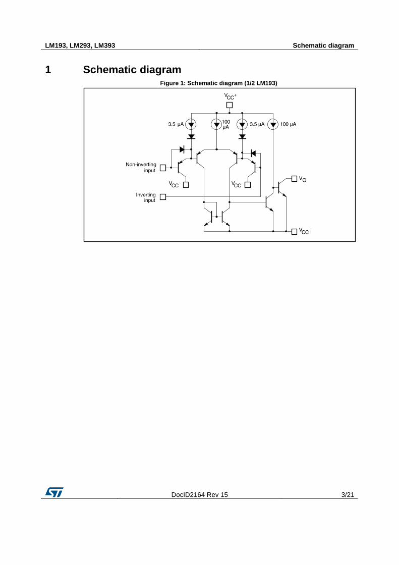
LM193, LM293, LM393 Schematic diagram
DocID2164 Rev 15 3/21
1 Schematic diagram Figure 1: Schematic diagram (1/2 LM193)
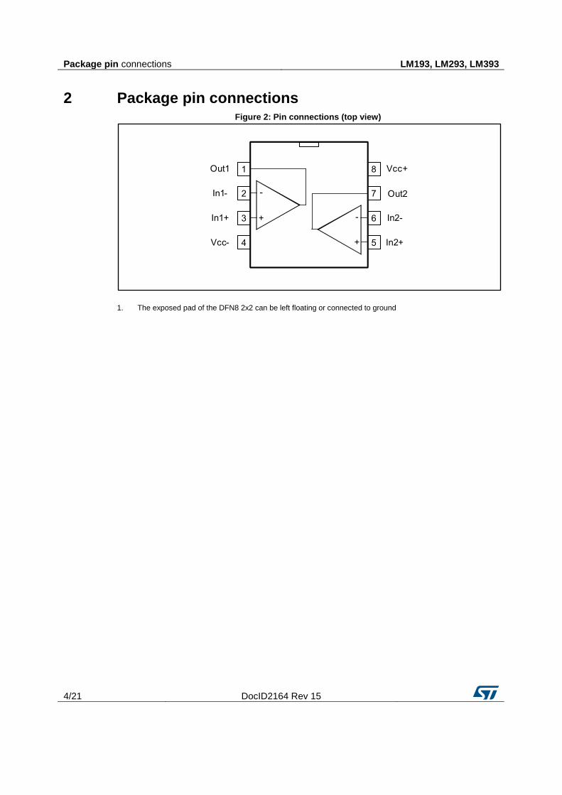
Package pin connections LM193, LM293, LM393
4/21 DocID2164 Rev 15
2 Package pin connections Figure 2: Pin connections (top view)
1. The exposed pad of the DFN8 2x2 can be left floating or connected to ground

LM193, LM293, LM393 Absolute maximum ratings and operating conditions
DocID2164 Rev 15 5/21
3 Absolute maximum ratings and operating conditions Table 1: Absolute maximum ratings
Symbol Parameter Value Unit
VCC Supply voltage ±18 or 36
V Vid Differential input voltage ±36
Vin Input voltage -0.3 to 36
Output short-circuit to ground
(1) Infinite
Rthja Thermal resistance junction to ambient (2)
DFN8 2x2 57
°C/W
MiniSO8 190
TSSOP8 120
SO8 125
Rthjc Thermal resistance junction to case (2)
DFN8 2x2 —
MiniSO8 39
TSSOP8 37
SO8 40
Tj Maximum junction temperature 150 °C
Tstg Storage temperature range -65 to 150
ESD class (3)
HBM: human body model (4)
H1B
MM: machine model
(5) M2
CDM: charged device model (6)
C5
Notes: (1)
Short-circuits from the output to VCC+ can cause excessive heating and potential destruction. The maximum output current is
approximately 20 mA independent of the magnitude of VCC+. (2)
Short-circuits can cause excessive heating and destructive dissipation. Values are typical. (3)
ESD class definition from AEC-Q100: (4)
HBM class H1B: ESD voltage level from 500 V to 1000 V (5)
MM class M2: ESD voltage level from 100 V to 200 V (6)
CDM class C5: ESD voltage level greater than 1500 V.

Absolute maximum ratings and operating conditions
LM193, LM293, LM393
6/21 DocID2164 Rev 15
Table 2: Operating conditions
Symbol Parameter Value Unit
VCC Supply voltage (VCC+) - (VCC
-) 2 to 36
V Vicm Common mode input voltage range (VCC
+ = 30 V)
(1)
Tamb = 25 °C 0 to (VCC+) - 1.5
Tmin ≤ Tamb ≤ Tmax 0 to (VCC+) - 2
Toper Operating free-air temperature range
LM193, LM193A -55 to 125
°C LM293, LM293A -40 to 105
LM393, LM393A 0 to 70
Notes: (1)
The input common-mode voltage of either input signal voltage should not be allowed to go negative by more than 0.3 V. The
high end of the common-mode voltage range is (VCC+) - 1.5 V, but either or both inputs can go to 30 V without damage.

LM193, LM293, LM393 Electrical characteristics
DocID2164 Rev 15 7/21
4 Electrical characteristics Table 3: VCC+ = 5 V, VCC- = 0 V, Tamb = 25 °C (unless otherwise specified)
Symbol Parameter Condition
LM193A, LM293A,
LM393A
LM193, LM293,
LM393 Unit
Min. Typ. Max. Min Typ. Max.
Vio Input offset
voltage (1)
1 2
1 5 mV
Tmin ≤ Tamb ≤ Tmax
4
9
Iio Input offset current 3 25
3 50
nA Tmin ≤ Tamb ≤ Tmax
100
150
Iib Input bias current
(I+ or I
-)
(2)
20 100
20 250
Tmin ≤ Tamb ≤ Tmax
300
400
Avd Large signal
voltage gain
VCC = 15 V, RL = 15 kΩ,
Vo = 1 V to 11 V 50 200
50 200
V/mV
ICC Supply current
(all comparators)
VCC = 5 V, no load
0.45 1
0.45 1 mA
VCC = 30 V, no load
0.6 2.5
0.6 2.5
Vid Differential input
voltage (3)
VCC
+
VCC
+
VOL Low-level output
voltage
Vid = -1 V, Isink = 4 mA
80 400
80 400 mV
Tmin ≤ Tamb ≤ Tmax
700
700
IOH High-level output
current
VCC = Vo = 30 V,
Vid = 1 V 0.1
0.1
nA
Tmin ≤ Tamb ≤ Tmax
1
1 μA
Isink Output sink current Vid = 1 V, Vo = 1.5 V 6 18
6 18
mA
tre Response time (4)
RL = 5.1 kΩ connected
to VCC+
1.3
1.3
μs
trel Large signal
response time
RL = 5.1 kΩ connected
to VCC+, el = TTL,
V(ref) = 1.4 V 300
300
ns
Notes: (1)
At output switch point, Vo = 1.4 V, Rs = 0 with VCC+ from 5 V to 30 V, and over the full common-mode range
(0 V to (VCC+) - 1.5 V).
(2)The direction of the input current is out of the IC due to the PNP input stage. This current is essentially constant, independent of
the state of the output, so no loading charge exists on the reference of input lines. (3)
Positive excursions of input voltage may exceed the power supply level. As long as the other voltage remains within the common-mode range, the comparator will provide a proper output state. The low input voltage state must not be less than -0.3 V (or 0.3 V below the negative power supply, if used). (4)
The response time specified is for a 100 mV input step with 5 mV overdrive. For larger overdrive signals, 300 ns can be obtained.

Electrical characteristic curves LM193, LM293, LM393
8/21 DocID2164 Rev 15
5 Electrical characteristic curves
Figure 3: Supply current vs. supply voltage
Figure 4: Input current vs. supply voltage
Figure 5: Output saturation voltage vs. output current
Figure 6: Response time for various input
overdrives - negative transition
Figure 7: Response time for various input overdrives - positive transition

LM193, LM293, LM393 Typical applications
DocID2164 Rev 15 9/21
6 Typical applications
Figure 8: Basic comparator
Figure 9: Driving TTL
Figure 10: Low-frequency op amp (1)
Figure 11: Driving CMOS
Figure 12: Low-frequency op amp (2)
Figure 13: Transducer amplifier
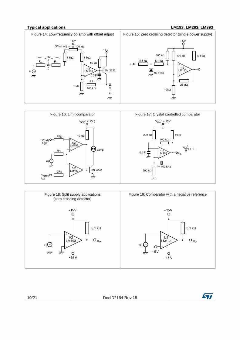
Typical applications LM193, LM293, LM393
10/21 DocID2164 Rev 15
Figure 14: Low-frequency op amp with offset adjust
Figure 15: Zero crossing detector (single power supply)
Figure 16: Limit comparator
Figure 17: Crystal controlled comparator
Figure 18: Split supply applications
(zero crossing detector)
Figure 19: Comparator with a negative reference

LM193, LM293, LM393 Typical applications
DocID2164 Rev 15 11/21
Figure 20: Two-decade, high-frequency VCO

Package information LM193, LM293, LM393
12/21 DocID2164 Rev 15
7 Package information
In order to meet environmental requirements, ST offers these devices in different grades of ECOPACK
® packages, depending on their level of environmental compliance. ECOPACK
®
specifications, grade definitions and product status are available at: www.st.com. ECOPACK
® is an ST trademark.

LM193, LM293, LM393 Package information
DocID2164 Rev 15 13/21
7.1 DFN8 2x2 package information
Figure 21: DFN8 2x2 package outline
Table 4: DFN8 2x2 mechanical data
Ref.
Dimensions
Millimeters Inches
Min. Typ. Max. Min. Typ. Max.
A 0.51 0.55 0.60 0.020 0.022 0.024
A1
0.05
0.002
A3
0.15
0.006
b 0.18 0.25 0.30 0.007 0.010 0.012
D 1.85 2.00 2.15 0.073 0.079 0.085
D2 1.45 1.60 1.70 0.057 0.063 0.067
E 1.85 2.00 2.15 0.073 0.079 0.085
E2 0.75 0.90 1.00 0.030 0.035 0.039
e
0.50
0.020
L
0.425
0.017
ddd
0.08
0.003

Package information LM193, LM293, LM393
14/21 DocID2164 Rev 15
Figure 22: DFN8 2x2 recommended footprint
LM193, LM293, LM393 Package information
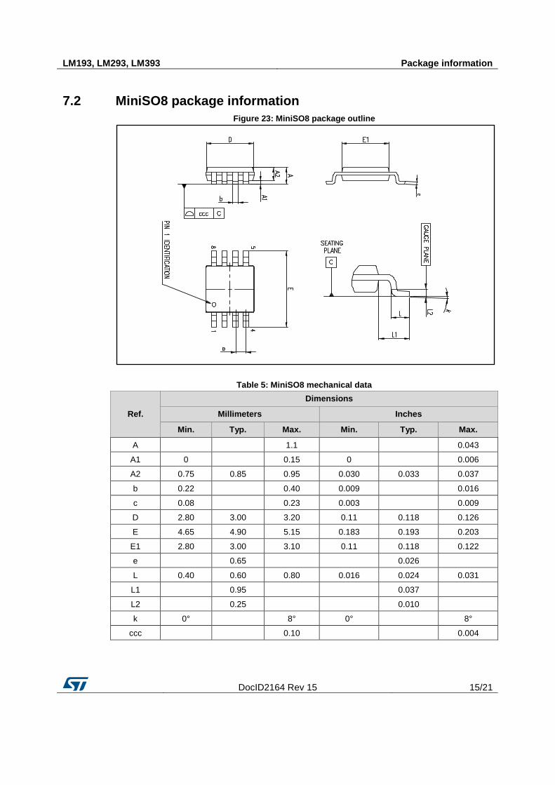
DocID2164 Rev 15 15/21
7.2 MiniSO8 package information
Figure 23: MiniSO8 package outline
Table 5: MiniSO8 mechanical data
Ref.
Dimensions
Millimeters Inches
Min. Typ. Max. Min. Typ. Max.
A
1.1
0.043
A1 0
0.15 0
0.006
A2 0.75 0.85 0.95 0.030 0.033 0.037
b 0.22
0.40 0.009
0.016
c 0.08
0.23 0.003
0.009
D 2.80 3.00 3.20 0.11 0.118 0.126
E 4.65 4.90 5.15 0.183 0.193 0.203
E1 2.80 3.00 3.10 0.11 0.118 0.122
e
0.65
0.026
L 0.40 0.60 0.80 0.016 0.024 0.031
L1
0.95
0.037
L2
0.25
0.010
k 0°
8° 0°
8°
ccc
0.10
0.004
Package information LM193, LM293, LM393
16/21 DocID2164 Rev 15
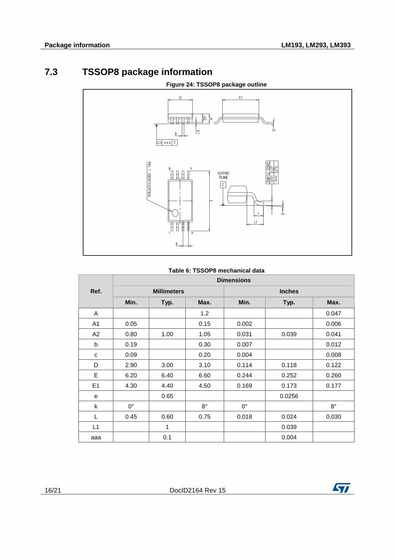
7.3 TSSOP8 package information
Figure 24: TSSOP8 package outline
Table 6: TSSOP8 mechanical data
Ref.
Dimensions
Millimeters Inches
Min. Typ. Max. Min. Typ. Max.
A
1.2
0.047
A1 0.05
0.15 0.002
0.006
A2 0.80 1.00 1.05 0.031 0.039 0.041
b 0.19
0.30 0.007
0.012
c 0.09
0.20 0.004
0.008
D 2.90 3.00 3.10 0.114 0.118 0.122
E 6.20 6.40 6.60 0.244 0.252 0.260
E1 4.30 4.40 4.50 0.169 0.173 0.177
e
0.65
0.0256
k 0°
8° 0°
8°
L 0.45 0.60 0.75 0.018 0.024 0.030
L1
1
0.039
aaa
0.1
0.004
LM193, LM293, LM393 Package information
DocID2164 Rev 15 17/21
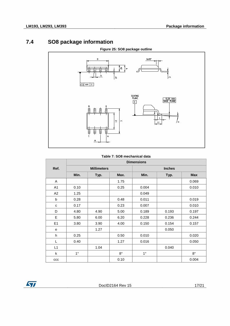
7.4 SO8 package information
Figure 25: SO8 package outline
Table 7: SO8 mechanical data
Ref.
Dimensions
Millimeters Inches
Min. Typ. Max. Min. Typ. Max
A
1.75
0.069
A1 0.10
0.25 0.004
0.010
A2 1.25
0.049
b 0.28
0.48 0.011
0.019
c 0.17
0.23 0.007
0.010
D 4.80 4.90 5.00 0.189 0.193 0.197
E 5.80 6.00 6.20 0.228 0.236 0.244
E1 3.80 3.90 4.00 0.150 0.154 0.157
e
1.27
0.050
h 0.25
0.50 0.010
0.020
L 0.40
1.27 0.016
0.050
L1
1.04
0.040
k 1°
8° 1°
8°
ccc
0.10
0.004

Ordering information LM193, LM293, LM393
18/21 DocID2164 Rev 15
8 Ordering information Table 8: Order codes
Order code Temperature range Package Packing Marking
LM193ADT (1)
-55 °C to 125 °C
SO8 Tube or tape and reel
193A
LM193DT 193
LM293ADT
-40 °C to 105 °C
293A
LM293D
293 LM293DT
LM293PT TSSOP8
Tape and reel LM293ST MiniSO8 K512
LM293QT DFΝ8 2x2 K59
LM393ADT
0 °C to 70 °C
SO8 Tube or tape and reel
393A
LM393D
393 LM393DT
LM393PT TSSOP8
Tape and reel LM393ST MiniSO8 M393
LM393QT DFΝ8 2x2 K5B
Notes: (1)
Not recommended for new design (NRND)

LM193, LM293, LM393 Revision history
DocID2164 Rev 15 19/21
9 Revision history Table 9: Document revision history
Date Revision Changes
02-Jul-2002 1 First release.
02-Jan-2005 2 Class A of the product included in the datasheet.
02-May-2005 3 PPAP references inserted in the datasheet, see Table 7: Ordering
information on page 18.
02-Jul-2005 4 Modification on PPAP references - Errors on part numbers, see
Table 7: Ordering information on page 18.
22-Nov-2005 5 Modification on Table 3 on page 6. LM293,A must be -40/+105°C
instead of -40/+125°C.
16-Feb-2006 6 Unit error for Vol parameter see Table 3 on page 6.
23-Aug-2007 7
Corrected error in DIP8 package information related to lead thickness,
see Figure 21 on page 12.
Added values for Rthja and Rthjc, and ESD parameters in Table 1:
Absolute maximum ratings.
08-Nov-2007 8
Updated MiniSO-8 package information.
Reformatted package information.
Added automotive grade order codes.
19-Feb-2008 9 Corrected error in SO-8 package mechanical data: E dimension in
drawing was marked with an F in table.
15-Dec-2008 10 Corrected heading in Figure 5.
22-Feb-2010 11 Deleted automotive grade order codes for LM293 and LM393.
22-Jun-2011 12
Updated typical performance curves.
Updated typical values on Table 3 on page 6.
Updated ESD parameters with ESD classes in Table 1: Absolute
maximum ratings.
Added DFN8 2x2mm package mechanical drawing.
Added DFN8 2x2mm recommended footprint.
Added DFN8 2x2mm order codes in Table 9.
27-Jun-2012 13
Updated Features (added package information), Description (added
RPNs), Figure 1: Pin connections (top view) moved to page 3, added
Contents, updated marking of the LM293QT device in Table 9, minor
text corrections throughout document.
18-Jan-2013 14 Updated Table 8 (added dimensions in inches).

Revision history LM193, LM293, LM393
20/21 DocID2164 Rev 15
Date Revision Changes
09-Feb-2016 15
Updated document layout
Removed DIP8 package
Features: removed “plastic micropackage” from the DFN8 2x2,
MiniSO8, and SO8 silhouettes; removed “thin shrink small outline
package” from the TSSOP8 silhouette.
Figure 2: added footnote about the exposed pad of the DFN8 2x2
Table 4: updated “L” value
Table 6: “aaa” value is a typ. value not a max. value
Table 7: updated min. “k” millimeters value
Table 8: removed following obsolete order codes: LM193AD, LM193D,
LM193AN, LM193N, LM293AD, LM293AN, LM293N, LM393AD,
LM393AN, LM393N; added footnote (not recommended for new
design) to order code LM193ADT; replaced marking of LM393QT with
“K5B” instead of “K5C”.

LM193, LM293, LM393
DocID2164 Rev 15 21/21
IMPORTANT NOTICE – PLEASE READ CAREFULLY
STMicroelectronics NV and its subsidiaries (“ST”) reserve the right to make changes, corrections, enhancements, modifications , and improvements to ST products and/or to this document at any time without notice. Purchasers should obtain the latest relevant information on ST products before placing orders. ST products are sold pursuant to ST’s terms and conditions of sale in place at the time of order acknowledgement.
Purchasers are solely responsible for the choice, selection, and use of ST products and ST assumes no liability for application assistance or the design of Purchasers’ products.
No license, express or implied, to any intellectual property right is granted by ST herein.
Resale of ST products with provisions different from the information set forth herein shall void any warranty granted by ST for such product.
ST and the ST logo are trademarks of ST. All other product or service names are the property of their respective owners.
Information in this document supersedes and replaces information previously supplied in any prior versions of this document.
© 2016 STMicroelectronics – All rights reserved