low-power robust design
TRANSCRIPT

1
Welcome to the Welcome to the Low Power Robust Computing Low Power Robust Computing
TutorialTutorial
Todd Austin, David Blaauw,Todd Austin, David Blaauw,KrisztiKrisztiáán Flautner, Nam Sung Kim,n Flautner, Nam Sung Kim,
Trevor Mudge, Dennis SylvesterTrevor Mudge, Dennis Sylvester
IntroductionIntroduction
Trevor MudgeTrevor [email protected]@umich.edu
The University of MichiganThe University of Michigan
Thanks to:Thanks to:Shaun DShaun D’’Souza, Taeho Kgil & Dave RobertsSouza, Taeho Kgil & Dave Roberts

2
Past Tutorials& WorkshopsPast Tutorials& WorkshopsPowerPower--Driven Microarchitecture Workshop Driven Microarchitecture Workshop –– ISCA98, ISCA98, Barcelona, Spain, June, 1998. Barcelona, Spain, June, 1998.
D. Grunwald, S. Manne, T. MudgeD. Grunwald, S. Manne, T. MudgeCool Chips Tutorial (Cool Chips Tutorial (An Industrial Perspective on Low An Industrial Perspective on Low Power Processor Design) Power Processor Design) –– MICRO 32, Haifa, Israel, MICRO 32, Haifa, Israel,
D. Grunwald, S. Manne, T. MudgeD. Grunwald, S. Manne, T. MudgeKool Chips Workshop Kool Chips Workshop –– MICRO33, Monterey, CA, MICRO33, Monterey, CA, Dec., 2000. Dec., 2000.
D. Grunwald, M. Irwin, T. MudgeD. Grunwald, M. Irwin, T. Mudge
Single thread performance waswas still king
Evolution of a 90Evolution of a 90’’s Highs High--End ProcessorEnd Processor
CompaqCompaq’’s Alphas Alpha
67 A @ 100 W67 A @ 100 W
Power density 30 W/cmPower density 30 W/cm2 2
Power(Watts)
Freq.(MHz)
Die Size(mm 2)
Vdd
Alpha21064
30 200 234 3.3
Alpha21164
50 300 299 3.3
Alpha21264
72 667 302 2.0
Alpha21364
100 1000 350 1.5

3
But there was another viewpointBut there was another viewpoint
ISLPED had been going strong for several ISLPED had been going strong for several yearsyears
Design Automation Conference had fostered Design Automation Conference had fostered low power studieslow power studies
Manufacturers of untethered devices were Manufacturers of untethered devices were acutely aware of power needsacutely aware of power needs
High 90High 90’’s Digital Signal Processors Digital Signal Processor
Analog Devices 21160 SHARCAnalog Devices 21160 SHARC•• 600 Mflops @ 2W600 Mflops @ 2W•• 100 Mhz SIMD with 6 computational units100 Mhz SIMD with 6 computational units
Recognized that parallelism saves powerRecognized that parallelism saves powerHad the right workload to exploit this factHad the right workload to exploit this fact
[We will see that the story has become more complicated][We will see that the story has become more complicated]

4
Why does power matter?Why does power matter?
“…“… left unchecked, power consumption will left unchecked, power consumption will reach 1200 Watts for highreach 1200 Watts for high--end processors in end processors in 2018. 2018. …… power consumption [is] a major power consumption [is] a major shows topper with offshows topper with off--state current leakage state current leakage ‘‘a a limiter of integrationlimiter of integration’’..””
Intel chairman Andrew Grove Intel chairman Andrew Grove Int. Electron Int. Electron Devices MeetingDevices Meeting keynote Dec. 2002keynote Dec. 2002
Why does robustness matter?Why does robustness matter?…… the ability to consistently resolve critical dimensions of 30nmthe ability to consistently resolve critical dimensions of 30nmis severely compromised creating substantial uncertainty in is severely compromised creating substantial uncertainty in device performance. ... at 30nm design will enter an era of device performance. ... at 30nm design will enter an era of ““probabilistic computing,probabilistic computing,”” with the behavior of logic gates no with the behavior of logic gates no longer deterministiclonger deterministic……susceptibility to single event upsets from radiation particle susceptibility to single event upsets from radiation particle strikes will grow due to supply voltage scaling while power strikes will grow due to supply voltage scaling while power supply integrity (IR drop, inductive noise, electromigration supply integrity (IR drop, inductive noise, electromigration failure) will be exacerbated by rapidly increasing current demanfailure) will be exacerbated by rapidly increasing current demand d new approaches to robust and low power design will be crucial new approaches to robust and low power design will be crucial to the successful continuation of process scaling ... to the successful continuation of process scaling ...
Intel chairman Andrew Grove Intel chairman Andrew Grove Int. Electron Devices MeetingInt. Electron Devices Meeting keynote keynote Dec. 2002Dec. 2002

5
Power and RobustnessPower and Robustness““.. power has become a first order concern at the 90nm node... power has become a first order concern at the 90nm node.””"The new paradigm for us as designers is that we are designing "The new paradigm for us as designers is that we are designing to a fixed performance instead of a fixed voltage," to a fixed performance instead of a fixed voltage," ““I know what kind of voltage I want to achieve, the question is I know what kind of voltage I want to achieve, the question is ‘‘what kind of voltage variation can I make and still achieve the what kind of voltage variation can I make and still achieve the required level of performance?required level of performance?’’ ””“…“… EDA vendors need to develop technologies that allow EDA vendors need to develop technologies that allow designers to use multiple voltage domains and employ robust designers to use multiple voltage domains and employ robust electrical rule checking ... tools need to better understand electrical rule checking ... tools need to better understand boundary conditions and variable Vdd ..boundary conditions and variable Vdd ..””““Tools also need to support multiple Vt libraries and need to Tools also need to support multiple Vt libraries and need to help users apply help users apply ““sleepsleep”” and and ““drowsy modesdrowsy modes”” on logic in on logic in addition to memory higher up in the design flowaddition to memory higher up in the design flow…”…”
Texas Instruments Fellow, Peter Rickert Texas Instruments Fellow, Peter Rickert ICCADICCAD keynote Nov. 2004keynote Nov. 2004
Power is a 1Power is a 1stst Class Design ConstraintClass Design Constraint
For untethered computing devices For untethered computing devices –– ObviousObvious

6
For Aggregated Systems tooFor Aggregated Systems too
Internet Service ProviderInternet Service Provider’’s Data Centers Data CenterHeavy duty factory Heavy duty factory –– 25,000 sq. ft. ~8,000 servers, ~2,000,000 Watts25,000 sq. ft. ~8,000 servers, ~2,000,000 WattsWant lowest cost/server/sq. ft.Want lowest cost/server/sq. ft.Cost a function of:Cost a function of:•• cooling air flowcooling air flow•• power deliverypower delivery•• racking heightracking height•• maintenance costmaintenance cost•• lead cost driver is power ~25%lead cost driver is power ~25%
Total Power of CPUs in PCsTotal Power of CPUs in PCs
Early Early ’’9090’’s s –– 100M CPUs @ 1.8W = 180MW100M CPUs @ 1.8W = 180MWEarly 21Early 21stst –– 500M CPUs @ 18W = 10,000MW500M CPUs @ 18W = 10,000MWExponential growthExponential growthRecent comment in a Financial Times article: Recent comment in a Financial Times article: 10% of US10% of US’’s energy use is for computerss energy use is for computers•• exponentially growth implies it will overtake exponentially growth implies it will overtake
cars/homes/manufacturingcars/homes/manufacturing
NOT! NOT! –– why wewhy we’’re herere here

7
What hasnWhat hasn’’t followed Mooret followed Moore’’s Laws Law
Batteries have onlyBatteries have onlyimproved their powerimproved their powercapacity by aboutcapacity by about5% every two years5% every two years
Low power has other implications Low power has other implications ……
Low power has been the technology that defines Low power has been the technology that defines mainstream computing technologymainstream computing technology•• Vacuum tubes Vacuum tubes →→ siliconsilicon•• TTL TTL →→ CMOS CMOS •• microprocessorsmicroprocessors
19501950’’s s ““supercomputerssupercomputers”” created the technologycreated the technology19801980’’s supercomputer were the beneficiaries of s supercomputer were the beneficiaries of microprocessor technologymicroprocessor technology19901990’’s microprocessors led to PDAs/cell phones/etcs microprocessors led to PDAs/cell phones/etcWill the tethered computers of the 21Will the tethered computers of the 21stst century be century be the beneficiaries of mobile computer technologythe beneficiaries of mobile computer technology

8
Why does robustness matter?Why does robustness matter?
GroveGrove’’s commentss comments•• SEUsSEUs•• IR dropIR drop•• inductive noiseinductive noise•• Electromigration, etc.Electromigration, etc.
Increase in variability as feature sizes decrease Increase in variability as feature sizes decrease Likely to be the next major challengeLikely to be the next major challenge•• strengthen interest in faultstrengthen interest in fault--tolerancetolerance•• renew interest in selfrenew interest in self--healinghealing
How are they related?How are they related?
The move to smaller features can help with The move to smaller features can help with power power –– with qualificationswith qualificationsSmaller features increase design marginsSmaller features increase design margins•• reduce power savingsreduce power savings•• reduce performance gainsreduce performance gains•• reduced area benefitsreduced area benefits

9
ChallengesChallengesPower density is growingPower density is growingSystems are becoming less robustSystems are becoming less robustCan architecture help?Can architecture help?
•• Lower power organizations Lower power organizations –– quick estimates of powerquick estimates of power•• Robust organizations Robust organizations –– quick estimates of robustnessquick estimates of robustness
By one account we need a 2x reduction in By one account we need a 2x reduction in power/generation from architecturepower/generation from architecture
Question where will the solution come fromQuestion where will the solution come from•• processprocess•• circuitscircuits•• architecturearchitecture•• OS OS •• languagelanguage
A System Challenge for the Near FutureA System Challenge for the Near Future
What the endWhat the end--users really want: supercomputer users really want: supercomputer performance in their pocketsperformance in their pockets……
•• Untethered operation, alwaysUntethered operation, always--on communicationson communications•• Driven by applications (games, positioning, advanced signal procDriven by applications (games, positioning, advanced signal processing, etc.)essing, etc.)
Mobile supercomputingMobile supercomputing
HighDensityStorage(1 Gbyte)
Energy Supply (1475 mA-hr @ 4oz)
CPU(10k SPECInt,
20% duty-cycle)
Soft-radio 4xCrypto-processing 4xAugmented reality 4xSpeech recognition 2xMobile Applications 2x
Workload Performance Req’ed(relative to fastest current design)
HighDensityStorage(1 Gbyte)
Energy Supply (1475 mA-hr @ 4oz)
CPU(10k SPECInt,
20% duty-cycle)
Soft-radio 4xCrypto-processing 4xAugmented reality 4xSpeech recognition 2xMobile Applications 2x
Workload Performance Req’ed(relative to fastest current design)
All with very tiny batteriesAll with very tiny batteries

10
Outline of the PresentationsOutline of the Presentations
David Blaauw (U. Michigan)David Blaauw (U. Michigan)•• Physical basis for power consumption in CMOSPhysical basis for power consumption in CMOS
Kris Flautner (ARM Ltd.)Kris Flautner (ARM Ltd.)•• SystemSystem--Level energy managementLevel energy management
Nam Sung Kim (Intel CRL)Nam Sung Kim (Intel CRL)•• Low power memory systemsLow power memory systems
Dennis Sylvester (U. Michigan)Dennis Sylvester (U. Michigan)•• Physical basis of variability Physical basis of variability
Todd Austin (U. Michigan)Todd Austin (U. Michigan)•• Robust computingRobust computing
ScheduleSchedule
8:30 a 8:30 a –– StartStart10:00 a 10:00 a –– BreakBreak10:30 a 10:30 a –– ResumeResumeNoon Noon –– LunchLunch1:00 p 1:00 p –– ResumeResume2:30 p 2:30 p –– BreakBreak3:00 p 3:00 p –– ResumeResume6:00 p 6:00 p –– ReceptionReception

1
Static and Dynamic Power Analysis Static and Dynamic Power Analysis and Circuit Level Reduction Methodsand Circuit Level Reduction Methods
David BlaauwDavid BlaauwBo ZhaiBo Zhai
University of MichiganUniversity of Michigan
OutlineOutline
Power Consumption in CMOS CircuitPower Consumption in CMOS CircuitDynamic Power Reduction MethodsDynamic Power Reduction MethodsSubthresholdSubthreshold Leakage AnalysisLeakage AnalysisGateGate--Leakage Analysis Leakage Analysis Leakage Reduction MethodsLeakage Reduction MethodsRemoving safety margin using RazorRemoving safety margin using Razor

2
Power SourcesPower SourcesTotal Power = Total Power = Dynamic Power + Static Power + Short Circuit PowerDynamic Power + Static Power + Short Circuit Power
Dynamic Power ConsumptionDynamic Power Consumption
Inverter initial state: Inverter initial state: Input 1Input 1Output 0Output 0
No dynamic powerNo dynamic power
10

3
Dynamic Power ConsumptionDynamic Power ConsumptionInput 1Input 1→→00•• Energy drawn from power Energy drawn from power
supply:supply:
•• Energy consumed by Energy consumed by PMOS:PMOS:
•• Power isPower is
20
)(
)(
dd
V
Odd
dd
supply
CV
dVCV
dttiV
dttPE
dd
=
⋅=
⋅=
⋅=
∫
∫∫
2
21
)()(
)(
dd
Odd
PMOS
CV
dttiVV
dttPE
=
⋅−=
⋅=
∫∫
2
21
ddPMOS fCVEfP =⋅=
Dynamic Power ConsumptionDynamic Power ConsumptionInput 0Input 0→→11•• Energy drawn from Energy drawn from
supply: 0supply: 0•• Energy consumed by Energy consumed by
NMOS equals to the NMOS equals to the energy stored on the energy stored on the capacitance:capacitance:
•• Power isPower is
2
21)( ddONMOS CVdttiVE =⋅= ∫
2
21
ddNMOS fCVEfP =⋅=

4
OutlineOutline
Power Consumption in CMOS CircuitPower Consumption in CMOS CircuitDynamic Power Reduction MethodsDynamic Power Reduction MethodsSubthresholdSubthreshold Leakage AnalysisLeakage AnalysisGateGate--Leakage Analysis Leakage Analysis Leakage Reduction MethodsLeakage Reduction MethodsRemoving safety margin using RazorRemoving safety margin using Razor
How to Reduce Dynamic PowerHow to Reduce Dynamic PowerMore generallyMore generally
To reduce dynamic To reduce dynamic power, we can reducepower, we can reduce
2
21
dddyn fCVP α= where iswhere is switching activityswitching activityα
–– clock gatingclock gatingCC –– sizing downsizing downff –– lower frequencylower frequencyVddVdd –– lower voltagelower voltage
α

5
Dynamic Power Reduction Dynamic Power Reduction -- Parallel ComputationParallel Computation
Vdd, fVdd/2, f/2 Vdd/2, f/2
2ddCVEnergy = 22
21)
2(2 dd
dd CVVCEnergy =⋅=
Energy reduced by 50%, but double the Energy reduced by 50%, but double the area and more leakagearea and more leakage
•• JustJust--inin--time Dynamic Voltage time Dynamic Voltage Scaling (DVS) Scaling (DVS) –– cubic energy cubic energy saving with duty cyclesaving with duty cycle
3
3
2
) *(
*)(
*
cycledutyf
f
tVCf
tPEnergy
Vdd
scaled
taskscaledSscaled
taskVscaled
∝
∝
=
=
Dynamic Power Reduction Dynamic Power Reduction -- DVSDVS
•• Clock/power gating Clock/power gating –– linear linear energy saving with duty energy saving with duty cyclecycle
) (***
cycledutytPtPEnergy
taskVdd
onVdd
==
Freq
Vdd
ttask
ton
Given dynamic workload Given dynamic workload –– scale frequency or voltagescale frequency or voltage

6
How Far Should We Scale Down the Voltage?How Far Should We Scale Down the Voltage?
333M333M--733M733M0.95V0.95V--1.55V1.55VIntel Intel XScaleXScale 8020080200
300M300M--1G1G0.8V0.8V--1.3V1.3VTransmetaTransmeta Crusoe TM5800Crusoe TM5800
153M153M--333M333M1.0V1.0V--1.8V1.8VIBM PowerPC 405LPIBM PowerPC 405LP
Frequency RangeFrequency RangeVoltage RangeVoltage Range
Traditional DVS (Dynamic Voltage Scaling)Traditional DVS (Dynamic Voltage Scaling)•• Scaling rang limited to less than Scaling rang limited to less than VddVdd/2/2
Minimum functional voltageMinimum functional voltage•• For an CMOS inverter is [For an CMOS inverter is [MeindlMeindl, JSSC 2000]:, JSSC 2000]:
~ 48mV for a typical 0.18~ 48mV for a typical 0.18μμm technologym technology)10ln
1ln(2,T
STlimitdd V
SVV
⋅+=
Is there a Minimum Energy Point?Is there a Minimum Energy Point?
2 x 10 -18
-14
SuperthresholdSuperthreshold regionregion•• Active energy scales down Active energy scales down
quadraticallyquadratically with with VddVdd•• Leakage power scales down linearly Leakage power scales down linearly
with with VddVdd, delay scales up almost , delay scales up almost linearly with 1/Vdd, leakage energy linearly with 1/Vdd, leakage energy stays approximately constant with stays approximately constant with VddVdd..
SubthresholdSubthreshold regionregion•• Active energy scales down Active energy scales down
quadraticallyquadratically with with VddVdd•• Leakage power scales down linearly Leakage power scales down linearly
with with VddVdd, delay scales up , delay scales up exponentially with exponentially with VddVdd, leakage , leakage energy scales up almost exponentially energy scales up almost exponentially with with VddVdd
•• Minimum Energy Point (Minimum Energy Point (VminVmin) takes ) takes place when leakage energy becomes place when leakage energy becomes comparable with active energycomparable with active energy
7
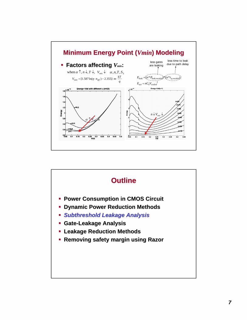
Minimum Energy Point (Minimum Energy Point (VminVmin) Modeling) Modeling
Factors affecting Factors affecting VVminmin::
↓↑ minVα
2
,, )*(*)*(
scaledSact
vscaledpvscaledleakleak
VnCE
tnPnE
=
=
less gates are leaking
less time to leak due to path delay
↓↓ minVn
SSTn ,,,α↓↓↓↑ minVTn , , ,when α
qkTmnV effmin ⋅⋅−⋅= ]355.2)ln(587.1[ η
OutlineOutline
Power Consumption in CMOS CircuitPower Consumption in CMOS CircuitDynamic Power Reduction MethodsDynamic Power Reduction MethodsSubthresholdSubthreshold Leakage AnalysisLeakage AnalysisGateGate--Leakage Analysis Leakage Analysis Leakage Reduction MethodsLeakage Reduction MethodsRemoving safety margin using RazorRemoving safety margin using Razor

8
Leakage Current ComponentsLeakage Current Components
SubthresholdSubthreshold leakage (Ileakage (Isubsub))•• Dominant when device is OFFDominant when device is OFF•• Enhanced by reduced VEnhanced by reduced Vt t
due to process scalingdue to process scaling
Gate tunneling leakage (IGate tunneling leakage (Igategate))•• Due to aggressive scaling of Due to aggressive scaling of
the gate oxide layer the gate oxide layer thickness (Tthickness (Toxox))
•• A super exponential function A super exponential function of Tof Toxox
•• Comparable to IComparable to Isubsub at 90nm at 90nm technologytechnology
Dual VDual Vtt AssignmentsAssignments
Transistor is assigned either a high or low Transistor is assigned either a high or low VtVt•• LowLow--VVtt transistor has reduced delay and transistor has reduced delay and
increased leakageincreased leakage
TradeTrade--off degrades for lower supply voltageoff degrades for lower supply voltage
Low-Vt; 0.9V High-Vt; 0.9V Low-Vt; 1.8V High-Vt; 1.8V
Leakage (norm) 1 0.06 1 0.07
Delay (norm) 1 1.30 1 1.20

9
Standby Leakage Estimation for Transistor StacksStandby Leakage Estimation for Transistor Stacks
Leakage current of a gate Leakage current of a gate depends on input statedepends on input stateConsider a 4Consider a 4--input NANDinput NAND•• For <1111>, the leakageFor <1111>, the leakage
current is determined bycurrent is determined bythe pull up networkthe pull up network
•• For other combinations,For other combinations,the leakage current isthe leakage current isdetermined by the determined by the pull down networkpull down network
•• So called So called stack effectstack effect
∑≤≤
=41 i
subpleak iII1.5V
1.5V
1.5V
1.5V
1.5V0V
(V(VDD DD = 1.5V, V= 1.5V, VT T = 0.25V)= 0.25V)
1.5V
1.5V
1.5V
1.5V
0V1.5V
0V
Iddq = 9.96nA
1.5V
0V
1.5V
1.5V
0V1.5V
55.9mV
Iddq = 1.71nA
0V
1.5V
0V
0V
1.5V
0V1.5V
76.1mV
Iddq = 0.98nA
20.2mV
0V
[Chen, et al., ISLPED98][Chen, et al., ISLPED98]
State Dependence (State Dependence (IIsubsub))
Simulation results of a 0.13um processSimulation results of a 0.13um process
Three OFF transistors in stackThree OFF transistors in stackOne OFF transistor in stackOne OFF transistor in stack
8X increase in leakage8X increase in leakage
Input ABC Output
Subthreshold Leakage (pA)
000 1 8.0836100 1 15.1873010 1 13.5167110 1 55.2532001 1 13.4401101 1 54.5532011 1 64.259111 0 191.2692
0
50
100
150
200
250
000 100 010 110 001 101 011 111
Input ABC
Subt
hres
hold
Lea
kage
(pA)
Source: F. Najm
10
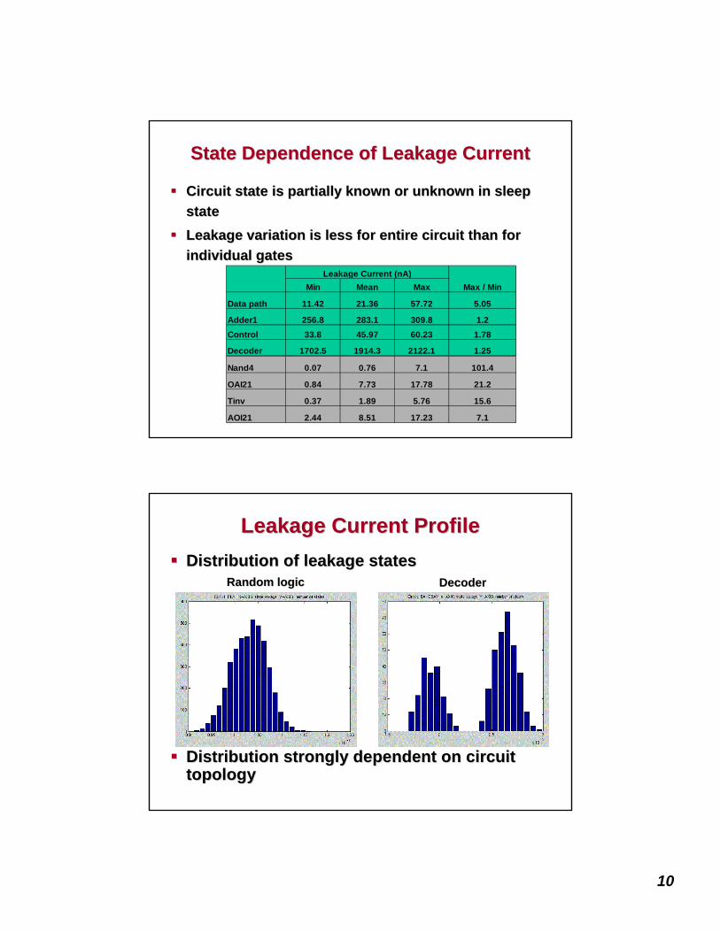
State Dependence of Leakage CurrentState Dependence of Leakage Current
Circuit state is partially known or unknown in sleep Circuit state is partially known or unknown in sleep statestateLeakage variation is less for entire circuit than for Leakage variation is less for entire circuit than for individual gatesindividual gates
Min Mean Max
Data path 11.42 21.36 57.72 5.05
Adder1 256.8 283.1 309.8 1.2Control 33.8 45.97 60.23 1.78
Decoder 1702.5 1914.3 2122.1 1.25
Nand4 0.07 0.76 7.1 101.4
OAI21 0.84 7.73 17.78 21.2
Tinv 0.37 1.89 5.76 15.6
AOI21 2.44 8.51 17.23 7.1
Leakage Current (nA)Max / Min
Leakage Current ProfileLeakage Current ProfileDistribution of leakage statesDistribution of leakage states
Distribution strongly dependent on circuit Distribution strongly dependent on circuit topologytopology
Random logicRandom logic DecoderDecoder
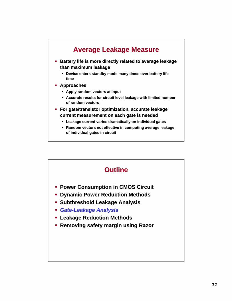
11
Average Leakage MeasureAverage Leakage MeasureBattery life is more directly related to average leakage Battery life is more directly related to average leakage than maximum leakagethan maximum leakage•• Device enters standby mode many times over battery life Device enters standby mode many times over battery life
timetime
ApproachesApproaches•• Apply random vectors at inputApply random vectors at input•• Accurate results for circuit level leakage with limited number Accurate results for circuit level leakage with limited number
of random vectorsof random vectors
For gate/transistor optimization, accurate leakage For gate/transistor optimization, accurate leakage current measurement on each gate is neededcurrent measurement on each gate is needed•• Leakage current varies dramatically on individual gatesLeakage current varies dramatically on individual gates•• Random vectors not effective in computing average leakage Random vectors not effective in computing average leakage
of individual gates in circuitof individual gates in circuit
OutlineOutline
Power Consumption in CMOS CircuitPower Consumption in CMOS CircuitDynamic Power Reduction MethodsDynamic Power Reduction MethodsSubthresholdSubthreshold Leakage AnalysisLeakage AnalysisGateGate--Leakage Analysis Leakage Analysis Leakage Reduction MethodsLeakage Reduction MethodsRemoving safety margin using RazorRemoving safety margin using Razor

12
Gate Oxide Leakage in an InverterGate Oxide Leakage in an InverterWhen input = VWhen input = Vdddd
•• NMOS: maximum INMOS: maximum Igategate
•• PMOS: maximum IPMOS: maximum Isubsub, reduced , reduced IIgategate
When input = 0VWhen input = 0V•• NMOS: VNMOS: Vgdgd=negative =negative
⇒⇒ IIgdgd: restricted to reverse gate : restricted to reverse gate tunnelingtunneling
maximum Imaximum Isubsub, reduced I, reduced Igategate
•• PMOS: small PMOS: small IIgategate
IIgategate & I& Isubsub
•• can be independently calculated and can be independently calculated and added for total leakageadded for total leakage
Igd
Igs
Isub
Vdd 0V
Igd
Isub
Vdd0V
Leakage Modeling (switch level)Leakage Modeling (switch level)Scenario 1 : Transistor positioned
• Above 0 or more conducting transistors
• Below 1 or more non-conducting transistors
Igate of transistor added to Isub of stack
Scenario 2: Transistor positioned• Above 1 or more non-conducting
transistors• Below 0 or more conducting
transistorsAdjacent nodes are near VDD and thus gate leakage can be ignored
Scenario 3: There is a non-conducting transistor above and below
• Igate depends on Isub
• Increases in Igate pinch off Isub

13
State Dependence (State Dependence (IIgategate))
Input ABC Output
Subthreshold Leakage (pA)
Gate Leakage (pA)
000 1 8.0836 200.0241100 1 15.1873 131.8958010 1 13.5167 192.9729110 1 55.2532 95.4877001 1 13.4401 327.9802101 1 54.5532 256.4272011 1 64.259 455.7905111 0 191.2692 486.6814
Lowest Subthreshold Lowest Subthreshold LeakageLeakage
Lowest Gate Lowest Gate LeakageLeakage
Gate Leakage is minimized whenGate Leakage is minimized when•• The bottom transistor in a stack The bottom transistor in a stack
is OFFis OFFThis forces intermediate nodes This forces intermediate nodes in the stack to be near VDDin the stack to be near VDD
•• All other transistors in the stack All other transistors in the stack are ONare ON
This allows the complementary This allows the complementary pullpull--up network transistors, up network transistors, which are in a parallel structure, which are in a parallel structure, to be OFFto be OFF
0
100
200
300
400
500
600
000 100 010 110 001 101 011 111
Input ABCLe
akag
e (p
A)
Subthreshold Leakage Gate Oxide Leakage
NAND3
Source: F. Najm
Leakage Current TrendsLeakage Current Trends
1.E+00
1.E+01
1.E+02
1.E+03
1.E+04
1990 1995 2000 2005 2010 2015 2020
NTRS '97ITRS '99ITRS '01
I OFF
@ 2
5°C
(nA/μm
)

14
Leakage ProjectionLeakage Projection
350
250
180
165
150
130
107 90 80 70 65 50 35 25
1.E-17
1.E-12
1.E-07
1.E-02
1.E+031990 1995 2000 2005 2010 2015 2020
YearC
urre
nt [u
A/um
]
Subthreshold current
Effective gate tunneling current
High-k dielectrics expected to reach mainstream
Technology node [nm]
Gate vs. SubGate vs. Sub--threshold Leakagethreshold Leakage
Leakage contribution Leakage contribution heavily topology heavily topology dependent dependent Gate leakage Gate leakage contribution: ~30%contribution: ~30%•• Expected to be 50% by Expected to be 50% by
next generationnext generation
Gate leakage greater Gate leakage greater for Nand structuresfor Nand structures•• Wider NMOS stackWider NMOS stack

15
Temperature DependenceTemperature DependenceTemperature across Temperature across chip varies chip varies significantlysignificantlySubSub--threshold leakage threshold leakage a strong function of a strong function of temperaturetemperatureGate leakage less Gate leakage less sensitive to sensitive to temperaturetemperatureGreater than 10% Greater than 10% variation /10 deg C variation /10 deg C
Source: R. Rao
OutlineOutline
Power Consumption in CMOS CircuitPower Consumption in CMOS CircuitDynamic Power Reduction MethodsDynamic Power Reduction MethodsSubthresholdSubthreshold Leakage AnalysisLeakage AnalysisGateGate--Leakage Analysis Leakage Analysis Leakage Reduction MethodsLeakage Reduction Methods•• MTCMOSMTCMOS•• Dual Dual VtVt•• State AssignmentState Assignment•• VTCMOSVTCMOS
Removing safety margin using RazorRemoving safety margin using Razor

16
Leakage Reduction OverviewLeakage Reduction Overview
Low Vt
Logic
High Vt
High Vt
Vdd
MTCMOS
Vdd
Variable Vt
Logic
Substrate or SOI back gate
Vt control
Variable VtDual Threshold State Assignment
0 1 1 0 1 0
Source: [Johnson, et al., DAC99]Source: [Johnson, et al., DAC99]
MTCMOS OverviewMTCMOS Overview
MTCMOS (Multi Threshold MTCMOS (Multi Threshold CMOS)CMOS)Active modeActive mode•• Low VLow Vtt circuit operationcircuit operation
Standby modeStandby mode•• Disconnect power supplies Disconnect power supplies
through high Vthrough high Vtt devicesdevicesFor fine grain sleep controlFor fine grain sleep control•• Sequential circuits must retain Sequential circuits must retain
statestateDual sleep devices are Dual sleep devices are needed for sneak paths in needed for sneak paths in state retaining latchesstate retaining latches [Mutoh[Mutoh,, et al.,et al., JSSC 8/95]JSSC 8/95]

17
State Retaining MTCMOS LatchState Retaining MTCMOS Latch
(Low Vth Inverter)
High Vth Inverters forState Retention
Setup Time Penalty
SBY
SBY
D
CK
Q
SBY
SBY
[Mutoh[Mutoh,, et al.,et al., JSSC 8/95]JSSC 8/95]
Sneak Leakage Path with Single Sleep TransistorSneak Leakage Path with Single Sleep Transistor
SBY
SBY
D
CK
Q
SBY
SBY
(Low Vth Inverter)
Need for both polarity high VNeed for both polarity high Vtt sleep devicessleep devices
0
1
[Mutoh[Mutoh,, et al.,et al., JSSC 8/95]JSSC 8/95]

18
Balloon LatchBalloon Latch
[Shigematsu, et al., JSSC 6/97][Shigematsu, et al., JSSC 6/97]
Retaining State through ScanRetaining State through Scan
Low Vt Logic
High Vt
Local Memory
Scan outScan in
Scan out state before entering standby modeScan out state before entering standby mode•• No state retaining flipNo state retaining flip--flop necessaryflop necessary•• Single footer is sufficientSingle footer is sufficient
NonNon--power gated memory neededpower gated memory neededUse existing scan circuitryUse existing scan circuitry•• Slower transition to/from standby mode Slower transition to/from standby mode

19
Addressing IAddressing Igategate in MTCMOSin MTCMOS
Use header instead of footer sleep transistorUse header instead of footer sleep transistor•• Relies on lower IRelies on lower Igategate in PMOS transistorin PMOS transistor
Low Vt
Logic
High Vt Gating
Vgnd
sleepLow Vt
Logic
High Vt Gating
Vsup
sleep
[[Hamzaoglu,Hamzaoglu, et al., ISLPED02]et al., ISLPED02]
Boosted Gate MOS (BGMOS)Boosted Gate MOS (BGMOS)
Use a thick oxide, high VUse a thick oxide, high Vtt sleep transistorsleep transistor•• Suppress both ISuppress both Isubsub and Iand Igategate
During active mode, overdrive sleep transistor During active mode, overdrive sleep transistor gate inputgate input
Low Vt / Thin Tox
Logic
High Vt / Thick Tox
Vgnd
Vdd
Gnd
Vdd
0V
Vboost
ActiveStandby
[[Inukai,Inukai, et al., CICC2000]et al., CICC2000]

20
Sizing of Sleep TransistorSizing of Sleep TransistorSleep transistor introduces Sleep transistor introduces additional supply voltage additional supply voltage dropdrop•• Degradation in performanceDegradation in performance•• Signal integrity issuesSignal integrity issues
Careful sizing of sleep Careful sizing of sleep transistor is neededtransistor is neededSharing virtual supply Sharing virtual supply between gates reduces between gates reduces voltage fluctuationvoltage fluctuation
[Kao[Kao,, et al., DAC97]et al., DAC97]
OutlineOutline
Power Consumption in CMOS CircuitPower Consumption in CMOS CircuitDynamic Power Reduction MethodsDynamic Power Reduction MethodsSubthresholdSubthreshold Leakage AnalysisLeakage AnalysisGateGate--Leakage Analysis Leakage Analysis Leakage Reduction MethodsLeakage Reduction Methods•• MTCMOSMTCMOS•• Dual Dual VtVt•• State AssignmentState Assignment•• VTCMOSVTCMOS
Removing safety margin using RazorRemoving safety margin using Razor

21
Dual VDual Vtt ExampleExample
Dual VDual Vtt assignment approachassignment approach•• Transistor on critical path: low VTransistor on critical path: low Vtt
•• NonNon--critical transistor: high critical transistor: high VVtt
0
0.2
0.4
0.6
0.8
1
All Low Vt Dual VtN
orm
aliz
ed L
eaka
ge c
urre
nt (Leakage Reduction)(1x)
(~2x)
VVtt Assignment GranularityAssignment GranularityVVtt assignment can be at different level of granularityassignment can be at different level of granularity•• Gate based assignmentGate based assignment•• Pull up network / Pull down network based assignmentPull up network / Pull down network based assignment
Single VSingle Vtt in P pull up or N pull down treesin P pull up or N pull down trees
•• Stack based assignmentStack based assignmentSingle VSingle Vtt in series connected transistorsin series connected transistors
•• Individually assignment within transistor stacksIndividually assignment within transistor stacksPossible area penaltyPossible area penalty
Number of library cells increases with finer controlNumber of library cells increases with finer control•• Better leakage / delay tradeBetter leakage / delay trade--offoff
Design rule constraint for
different Vt assignment

22
Example of Different VExample of Different Vtt Assignment GranularityAssignment Granularity
Gate
based
26.7%
PU/PD
based
63.5%
Stack
based
68.1%
Source: [Wei, et al., DAC99]Source: [Wei, et al., DAC99]
Simultaneous VSimultaneous Vtt, Size and V, Size and Vdddd Assignment Assignment -- ResultResult
Adding Adding VVdddd to W/Vto W/Vt t resulted in average resulted in average •• 60% decrease over W only60% decrease over W only•• 25% decrease over W/V25% decrease over W/Vtt..
0
1
2
3
4
5
6
7
8
Benchmark Circuit
Pow
er (m
W)
c17 c432 c499 c880 c1355 c1908 c2670 c3540 c5315 c6288 c7552
W, Vt, VDD
W, Vt
W
leakage
dynamic
[[NguyenNguyen,, et al., ISLPED03]et al., ISLPED03]
23
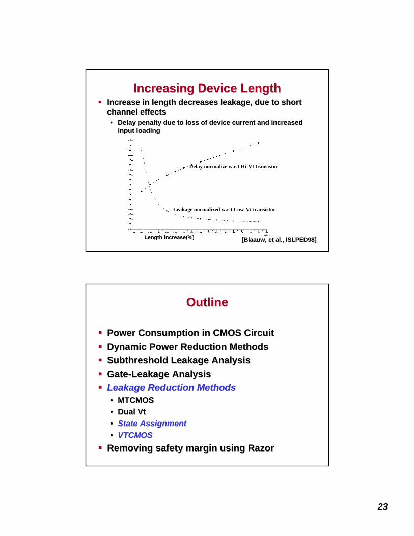
Increasing Device LengthIncreasing Device LengthIncrease in length decreases leakage, due to short Increase in length decreases leakage, due to short channel effectschannel effects•• Delay penalty due to loss of device current and increased Delay penalty due to loss of device current and increased
input loadinginput loading
Delay normalize w.r.t Hi-Vt transistor
Leakage normalized w.r.t Low-Vt transistor
Length increase(%) [Blaauw[Blaauw,, et al., ISLPED98]et al., ISLPED98]
OutlineOutline
Power Consumption in CMOS CircuitPower Consumption in CMOS CircuitDynamic Power Reduction MethodsDynamic Power Reduction MethodsSubthresholdSubthreshold Leakage AnalysisLeakage AnalysisGateGate--Leakage Analysis Leakage Analysis Leakage Reduction MethodsLeakage Reduction Methods•• MTCMOSMTCMOS•• Dual Dual VtVt•• State AssignmentState Assignment•• VTCMOSVTCMOS
Removing safety margin using RazorRemoving safety margin using Razor

24
Combining VCombining Vtt and Input State Assignmentand Input State AssignmentGiven a known input state in standby mode, Given a known input state in standby mode, only only ““OFFOFF”” transistors set to high Vtransistors set to high Vtt
All other transistors are kept at low VAll other transistors are kept at low Vtt
0
0.2
0.4
0.6
0.8
1
All Low Vt Dual Vt Randomstate
Nor
mal
ized
Lea
kage
cur
rent
(Leakage Reduction)(1x)
(~2x)
(~7.8x)
[[LeeLee,, et al., DAC03]et al., DAC03]
Combining VCombining Vtt and Input State Assignmentand Input State AssignmentOptimal input state with VOptimal input state with Vtt assignmentassignment•• Increased reduction of leakage currentIncreased reduction of leakage current
0
0.2
0.4
0.6
0.8
1
All Low Vt Dual Vt Randomstate
Optimalstate
Nor
mal
ized
Lea
kage
cur
rent (Leakage Reduction)
(1x)
(~2x)
(~7.8x)(~9.7x)
[[LeeLee,, et al., DAC03]et al., DAC03]

25
Stack Order Dependence of IStack Order Dependence of IgategateKey difference between the state dependence of IKey difference between the state dependence of Isubsub
and Iand Igategate•• IIsubsub primarily depends on the number of OFF transistors in stackprimarily depends on the number of OFF transistors in stack•• IIgategate depends strongly on the position of ON/OFF transistors in depends strongly on the position of ON/OFF transistors in
stackstack
IItotaltotalIIgategateIIsubsubStaStatete
47.247.28888
19.019.01515
28.228.27373
1111113.803.80
440.000.00
003.803.80
44110110
10.110.14343
6.336.3399
3.803.8044
1011010.670.67
660.000.00
000.670.67
66100100
18.318.30303
12.612.67777
5.625.6266
0110111.271.27
551.271.27
550.700.70
99010010
7.047.0488
6.336.3399
0.700.7099
0010010.380.38
220.000.00
000.380.38
22000000
0V
Igate
Vdd
VddIgate
Isub
IItotaltotalIIgategateIIsubsubStaStatete
47.247.28888
19.019.01515
28.228.27373
1111113.803.80
440.000.00
003.803.80
44110110
10.110.14343
6.336.3399
3.803.8044
1011010.670.67
660.000.00
000.670.67
66100100
18.318.30303
12.612.67777
5.625.6266
0110111.271.27
551.271.27
550.700.70
99010010
7.047.0488
6.336.3399
0.700.7099
0010010.380.38
220.000.00
000.380.38
22000000
Vdd
0V
Igate
Isub
Vdd
Igate = 0Vdd
0V Isub
Igate = 0
VddIgate = 0
IItotaltotalIIgategateIIsubsubStaStatete
47.247.28888
19.019.01515
28.228.27373
1111113.803.80
440.000.00
003.803.80
44110110
10.110.14343
6.336.3399
3.803.8044
1011010.670.67
660.000.00
000.670.67
66100100
18.318.30303
12.612.67777
5.625.6266
0110111.271.27
551.271.27
550.700.70
99010010
7.047.0488
6.336.3399
0.700.7099
0010010.380.38
220.000.00
000.380.38
22000000
~5x
Source: [Source: [LeeLee,, et al., DAC03]et al., DAC03]
OutlineOutline
Power Consumption in CMOS CircuitPower Consumption in CMOS CircuitDynamic Power Reduction MethodsDynamic Power Reduction MethodsSubthresholdSubthreshold Leakage AnalysisLeakage AnalysisGateGate--Leakage Analysis Leakage Analysis Leakage Reduction MethodsLeakage Reduction Methods•• MTCMOSMTCMOS•• Dual Dual VtVt•• State AssignmentState Assignment•• VTCMOSVTCMOS
Removing safety margin using RazorRemoving safety margin using Razor

26
VTCMOSVTCMOSVariable Threshold Variable Threshold CMOS CMOS (from T. Kuroda, ISSCC, (from T. Kuroda, ISSCC, 1996)1996)
In active mode:In active mode:•• Zero or slightly forward Zero or slightly forward
body biasbody biasfor high speedfor high speed
In standby mode:In standby mode:•• Deep reverse body bias Deep reverse body bias
for low for low leakageleakage
Triple well technology Triple well technology requiredrequired
Speed Adaptive Speed Adaptive VVtt CMOSCMOS
M. Miyazaki, et al, M. Miyazaki, et al, ““A 1.2A 1.2--GIPS/W GIPS/W uProcuProc Using Using SpeedSpeed--AdapativeAdapative VVtt CMOS with Forward Bias,CMOS with Forward Bias,””JSSC Feb 2002.JSSC Feb 2002.
Dynamically tune Dynamically tune VVtt so that so that critical path speed matched critical path speed matched clock periodclock periodReduces chipReduces chip--toto--chip parameter chip parameter variationsvariationsReverse bias:Reverse bias:Operate only as fast as necessary Operate only as fast as necessary
(reduces excess active (reduces excess active leakage)leakage)
Forward bias:Forward bias:Speeds up slow chipsSpeeds up slow chips
Standby leakage with maximum Standby leakage with maximum reverse biasreverse biasAlso known as Adaptive Body Also known as Adaptive Body Biasing (ABB)Biasing (ABB)

27
OutlineOutline
Power Consumption in CMOS CircuitPower Consumption in CMOS CircuitDynamic Power Reduction MethodsDynamic Power Reduction MethodsSubthresholdSubthreshold Leakage AnalysisLeakage AnalysisGateGate--Leakage Analysis Leakage Analysis Leakage Reduction MethodsLeakage Reduction MethodsRemoving safety margin using RazorRemoving safety margin using Razor
Impact of Process Scaling on DesignImpact of Process Scaling on DesignIncreasing uncertainty with Increasing uncertainty with process scalingprocess scaling•• InterInter-- and intraand intra--die process die process
variationsvariations•• Temperature variationTemperature variation•• Power supply dropPower supply drop•• Capacitive and inductive noiseCapacitive and inductive noise
Robust Design increasing difficultRobust Design increasing difficult•• Reduced yieldReduced yield•• Difficulty in design closureDifficulty in design closure•• WorstWorst--case design requires case design requires large large
safety marginssafety margins•• High energyHigh energy
Alarming uncertainty in Alarming uncertainty in NanotechnologiesNanotechnologies
Intra-die variations in ILD thickness

28
Robust Design for Low Power ApplicationsRobust Design for Low Power Applications
Low power antagonistic to robust Low power antagonistic to robust designdesignIncreased sensitivity to Vt Increased sensitivity to Vt variation in low voltage operationvariation in low voltage operation•• Dynamic voltage scalingDynamic voltage scaling•• Subthreshold voltage operationSubthreshold voltage operation
Clock gating and low power Clock gating and low power modes increase power grid noisemodes increase power grid noisePower optimization equalizes Power optimization equalizes circuit delaycircuit delay•• Number of paths that can lead to Number of paths that can lead to
chip failure dramatically increasedchip failure dramatically increasedFundamental challenge in nanometer Fundamental challenge in nanometer
design: design: Robust Robust andand Low Power Low Power DesignDesign
Criticalpath delay
delay
-- -- -- -- -- -- -- -
# of
pat
hsdelay
-- -- -- -- -- -- -- -
# of
pat
hs
POWER OPTIMIZATION
Robust Low Power DesignRobust Low Power DesignWorstWorst--case conditions highly improbablecase conditions highly improbable•• Many sources of variability are independent (process, noise, Many sources of variability are independent (process, noise,
SEU, supply drop) SEU, supply drop) •• Probability of all sources simultaneously having worstProbability of all sources simultaneously having worst--case case
condition very lowcondition very low•• ““guaranteed correctguaranteed correct”” design highly inefficientdesign highly inefficient
Common case design paradigmCommon case design paradigm•• Significant gain for circuits optimized for common caseSignificant gain for circuits optimized for common case
Efficiency mechanisms needed to tolerate infrequent Efficiency mechanisms needed to tolerate infrequent worstworst--case scenarioscase scenarios•• InIn--situ error detection and correction situ error detection and correction •• Dynamic runtime adjustment to silicon and environmental Dynamic runtime adjustment to silicon and environmental
conditionsconditions
29
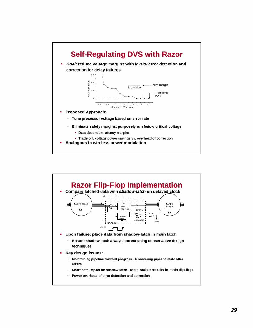
SelfSelf--Regulating DVS with RazorRegulating DVS with RazorGoal: Goal: reduce voltage margins with reduce voltage margins with inin--situsitu error detection and error detection and correction for delay failurescorrection for delay failures
Proposed Approach:Proposed Approach:•• Tune processor voltage based on error rateTune processor voltage based on error rate
•• Eliminate safety margins, purposely run Eliminate safety margins, purposely run belowbelow critical voltagecritical voltageDataData--dependent latency marginsdependent latency marginsTradeTrade--off: voltage power savings vs. overhead of correctionoff: voltage power savings vs. overhead of correction
Analogous to wireless power modulationAnalogous to wireless power modulation
0 . 8 1 . 0 1 . 2 1 . 4 1 . 6 1 . 8 2 . 0
0
2 0
4 0
6 0
S u p p l y V o l t a g e
Perc
enta
ge E
rror
s
Traditional DVS
Zero margin Sub-critical
Razor FlipRazor Flip--Flop ImplementationFlop ImplementationCompare latched data with Compare latched data with shadowshadow--latchlatch on delayed clockon delayed clock
Upon failure: place data from shadowUpon failure: place data from shadow--latch in main latchlatch in main latch•• Ensure shadow latch always correct using conservative design Ensure shadow latch always correct using conservative design
techniquestechniques
Key design issues:Key design issues:•• Maintaining pipeline forward progress Maintaining pipeline forward progress -- Recovering pipeline state after Recovering pipeline state after
errorserrors
•• Short path impact on shadowShort path impact on shadow--latch latch -- MetaMeta--stable results in main flipstable results in main flip--flopflop•• Power overhead of error detection and correctionPower overhead of error detection and correction
Errorcomparator
RAZOR FF
Main Flip-Flop
clk
clk_del
Shadow Latch
QLogic Stage
L1
Logic Stage
L2Error_L
01
D

30
inst2
IF
Razo
r FF ID
Razo
r FF EX
Razo
r FF MEM WB
(reg/mem)error
recover recover recover
Razo
r FF
PCrecover
errorerror error
clock
Cycle: 0inst1inst3inst4inst5
123456inst6
Centralized Pipeline Recovery ControlCentralized Pipeline Recovery Control
Once cycle penalty for timing failureOnce cycle penalty for timing failureGlobal synchronization may be difficult for fast, Global synchronization may be difficult for fast, complex designscomplex designsImplementation currently being explored for ARM 926 Implementation currently being explored for ARM 926 commercial corecommercial core
Distributed Pipeline Recovery ControlDistributed Pipeline Recovery Control
recover
IF
Razo
r FF ID
Razo
r FF EX
Razo
r FF MEM
(read-only)WB
(reg/mem)
error bubble
recover recover
Razo
r FF
Stab
ilizer
FF
PC
recover
flushID
bubble
error bubble
flushID
error bubble
flushIDFlushControl
flushID
error
Cycle: 0
inst1inst2inst3inst4inst5
123456
inst6 inst2inst7inst8
789
inst3inst4
Builds on existing branch / data speculation recovery Builds on existing branch / data speculation recovery frameworkframeworkMultiple cycle penalty for timing failureMultiple cycle penalty for timing failureScalable design since all recovery communication is Scalable design since all recovery communication is locallocalPrototype chip results availablePrototype chip results available

31
TradeTrade--Off in Razor DVSOff in Razor DVS
Total Energy
Optimal Voltage
Pipeline IPC
RecoveryEnergy
Supply Voltage
ProcessorEnergy
ProcessorEnergy w/ overhead
3.7mW3.7mWTotal Delay Buffer Power OverheadTotal Delay Buffer Power Overhead
2.9%2.9%% Total Chip Power Overhead% Total Chip Power Overhead
Error Correction and Recovery OverheadError Correction and Recovery Overhead
260fJ260fJEnergy of a RFF per error eventEnergy of a RFF per error event
60fJ/185fJ60fJ/185fJRFF Energy (Static/Switching)RFF Energy (Static/Switching)
49fJ/124fJ49fJ/124fJStandard FF Energy (Static/Switching)Standard FF Energy (Static/Switching)
Error Free Operation (Simulation Results)Error Free Operation (Simulation Results)
24982498Number of Delay Buffers AddedNumber of Delay Buffers Added
207207Total Number of Razor FlipTotal Number of Razor Flip--FlopsFlops
24082408Total Number of FlipTotal Number of Flip--FlopsFlops
8KB8KBDcache SizeDcache Size
8KB8KBIcache SizeIcache Size
130mW130mWMeasured Chip Power at 1.8VMeasured Chip Power at 1.8V
3.3mm*3.6mm3.3mm*3.6mmDie SizeDie Size
1.58million1.58millionTotal Number of TransistorsTotal Number of Transistors
1.21.2--1.8V1.8VDVS Supply Voltage RangeDVS Supply Voltage Range
120 120 -- 140MHz140MHzClock FrequencyClock Frequency
0.180.18µµmmTechnology NodeTechnology Node

32
Razor I Razor I -- Prototype TestbedPrototype Testbed
Razor I Razor I -- Prototype TestbedPrototype Testbed
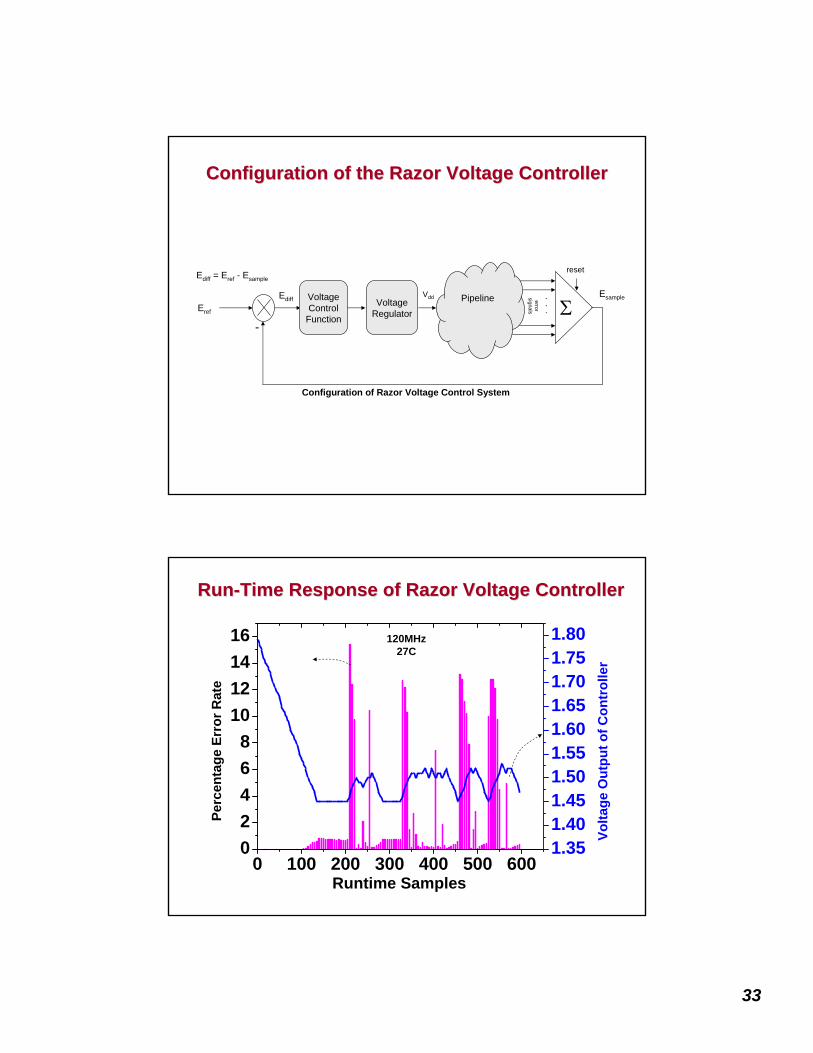
33
Eref
VoltageControl
FunctionΣ
.
.
.
Pipeline
reset
Vdd
Ediff = Eref - Esample
-
EsampleVoltage
Regulator
Ediff errorsignals
Configuration of Razor Voltage Control System
Configuration of the Razor Voltage ControllerConfiguration of the Razor Voltage Controller
Runtime Samples0 100 200 300 400 500 600
02468
10121416
1.351.401.451.501.551.601.651.701.751.80120MHz
27C
Perc
enta
ge E
rror
Rat
e
Volta
ge O
utpu
t of C
ontr
olle
rRunRun--Time Response of Razor Voltage ControllerTime Response of Razor Voltage Controller

34
QuestionsQuestions
????
????
??
?? ??
?? ??
??
????

1
Krisztián [email protected]
ARM Limited
SystemSystem--Level Energy ManagementLevel Energy Management
Talk, play, web, snap, video, organizeTalk for the massesTalk for brokersFeatures
125g205g800gWeight
$500$500$3995Price
Li-Ion, 21gNiMh, 100gLead Acid, 500gBattery
4h talk, 240h (>1 week) standby1h talk, 13h standby0.5h - 1h talk, 8h standbyBattery life
Nokia 6600Nokia 232Motorola DynaTAC 8000X
200319951983
Why does energy efficiency matter?Why does energy efficiency matter?
The disappearing battery - despite only incremental capacity improvements: the rest of the system has become more power efficient!Power has major impact on form factor, features, cost marketability

2
SmartSmart--phone system power budgetphone system power budget
Backlight alone often uses as much as 0.2W to 0.3WPhone is mostly off: leakage is already important!Bigger battery is not a good option• Adds bulk, cost, compromises consumer sex-appeal…
0.4 - 0.8Camera
0.2 - 0.3Voice recording
0.1 - 0.5
0.9 - 1
0.5 - 0.7
1
Smart-phone system power (W)during different operating modes
Phone call
Video playback
Gaming
Peak power
Higher performance, higher powerHigher performance, higher power
ARM7
ARM9
ARM11
1
10
100
1000
0 50 100 150 200 250 300 350 400 450 500
Dhrystone MIPS
Pow
er c
onsu
mpt
ion
(mW
)
0.18um process
0.13um process

3
ARM Power and silicon budgetsARM Power and silicon budgets
High performance is achieved at ~constant Si and power budgets• Enabled by process scaling
Transistors are not free: significant impact on Si and design cost• Architectural consistency is important to avoid legacy constraints
~same0.30.250.25Power (W)
32K+32K16K+16K8K+8K4K+4KCache
ARMv7ARMv6ARMv5TEJARMv4TArch
~same44.24.2Size (mm2)
0.0650.090.130.18Process
TigerARM1136J-S™ARM926EJ-S™ARM940T™Core
Some representative notebook specsSome representative notebook specs
Ultr
a-po
rtab
les
Des
ktop
repl
acem
ents

4
Notebook power consumptionNotebook power consumption
Backlight consumes between 0.5W and 3.5W depending on brightnessHard drive consumes 1W-2WMemory consumes betweenProcessor can be a significant fraction of total power consumedMisc. system components account for around 50% of powerFactor of 10-20 higher power consumption than in mobile phones
Based on data from www.crhc.uiuc.edu/~mahesri/ classes/project_report_cs497yyz.pdfData gathered on IBM ThinkPad R40 laptop (Pentium-M 1.3GHz, 14.1” display, 256M RAM)
Idleno DVS, high bright 15% 1% 8% 26% 13.13DVS, high bright 4% 1% 9% 29% 11.57DVS, low bright 5% 2% 13% 7% 8.23
No DVS, high brightProcessor bound 52% 1% 4% 13% 25.80Memory bound 43% 1% 5% 16% 21.40Hard drive bound 14% 1% 6% 19% 18.20Network bound 18% 15% 6% 20% 17.20Audio CD playback 17% 0% 6% 18% 19.20
Total (W)Power consumption
Workload Processor WiFi Backlight3D graphics
Backlights are power hungry!Backlights are power hungry!
Power consumption of a 3.8” Kyocera TFT LCD• http://americas.kyocera.com/kicc/Lcd/notes/powerconsump.htm
The power budget of the LCD + backlight is about 0.75W!

5
System vs. processor power System vs. processor power
Marketing doesnMarketing doesn’’t really care whether a feature t really care whether a feature is power hungry or notis power hungry or not……
…… spec to sell (e.g. bright backlight, small spec to sell (e.g. bright backlight, small battery)battery)…… optimize where you can, not necessary optimize where you can, not necessary where it would have the biggest pay offwhere it would have the biggest pay off
One area where we can / have to do something One area where we can / have to do something about power consumption is the processorabout power consumption is the processor
Overview Overview
Dynamic Voltage Scaling backgroundDynamic Voltage Scaling backgroundProcessor support for DVSProcessor support for DVSA role for asynchronous architectures?A role for asynchronous architectures?Software control of processor speedSoftware control of processor speedIs there more to speed setting than DVS?Is there more to speed setting than DVS?An example: ARM IEM Test ChipAn example: ARM IEM Test Chip

6
CMOS Power and Energy in a NutshellCMOS Power and Energy in a Nutshell
Power and Energy consumption trends of a workload running at different frequency and voltage levels.DFS: frequency scaling only, DVS: frequency & voltage scaling
Frequency
Volta
ge
Useful for DVS
Frequency
Pow
er
Frequency
Ener
gy
DFS
DFS
DVS
DVS
f ~ (vdd-vt)α / vdd
α ≈ 1.3vt / vmax ≈ 0.3
P = Cvdd2f + vddIleak
Avg. power ~ heatE = ∫Pdt
Need DVS to save energy
Must reduce voltage to save energy and extend battery life!
Performance scaling for energy efficiencyPerformance scaling for energy efficiency
Reduced processing rate enables more efficient operation• Use dynamic voltage scaling (DVS) and threshold scaling (ABB)
100%
0%
Utilization Work Work
Conventional system
100%
0%Work
Work
Scaled system
100%
0%
Power
100%
0%
100%
0%
Energy
100%
0%Time Time

7
RunRun--time performance scaling = BIG payoff time performance scaling = BIG payoff
Run-time performance scaling enables energy reduction• Dynamic Voltage Scaling• Threshold scaling (ABB) + DVS
Can be exploited in future process generations• Voltage is the only parameter that affects all types of power consumption: dynamic, static
(leakage), gate-oxide
Done under many different names• AMD PowerNow• ARM’s Intelligent Energy Manager (IEM)• IBM Dynamic Power Manager (DPM)• Intel SpeedStep, Wireless SpeedStep• Transmeta LongRun, LongRun2
Key: determining how fast a workload needs to run!
Source: Crusoe™ LongRun™ Power Management White Paper
TransmetaTransmeta’’ss ArgumentArgument
Simplified cooling (no fan) = cheaper systemsPerformance on demand = smaller battery is sufficient

8
IEM DemonstrationIEM Demonstration
2 seconds
Performance100%
83%
66%
50%
MPEG video
4 performance(frequency andvoltage) levelsavailable inbenchmarkedsystem
Performancelevel requestedby algorithm
Closest availableperformancelevel of system
LongRunLongRun Power ManagementPower Management
Source: Crusoe™ LongRun™ Power Management White Paper

9
Intel Enhanced Intel Enhanced SpeedStepSpeedStep
Next generation Speedstep supports more V,F settings10ms performance switch time Software algorithms to dynamically change settings based on performance statistics
Frequency Voltage1.6 GHz (HFM) 1.484 V1.4 GHz 1.420 V1.2 GHz 1.276 V1.0 GHz 1.164 V800 MHz 1.036 V600 MHz (LFM) 0.956 V
Pentium M 1.6 GHz
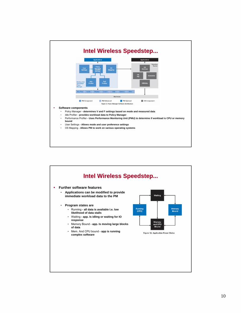
Intel Wireless Intel Wireless SpeedstepSpeedstep
Extends XScale power modesIncludes Power Manager (PM) softwareModes:• Standby• Voice Communications• Data Communications• Multimedia (Audio, Video and Camera)• Multimedia + Data Comms (Video Conferencing)
Emphasis on distinguising CPU-bound from memory-bound operation
10
Intel Wireless Intel Wireless SpeedstepSpeedstep......
Software components• Policy Manager - determines V and F settings based on mode and measured data• Idle Profiler - provides workload data to Policy Manager• Performance Profiler - Uses Performance Monitoring Unit (PMU) to determine if workload is CPU or memory
bound• User Settings - Allows mode and user preference settings• OS Mapping - Allows PM to work on various operating systems
Intel Wireless Intel Wireless SpeedstepSpeedstep......
Further software features• Applications can be modified to provide
immediate workload data to the PM
• Program states are• Running - all data is available I.e. low
likelihood of data stalls• Waiting - app. Is idling or waiting for IO
response• Memory Bound - app. Is moving large blocks
of data• Mem. And CPU bound - app is running
complex software
11
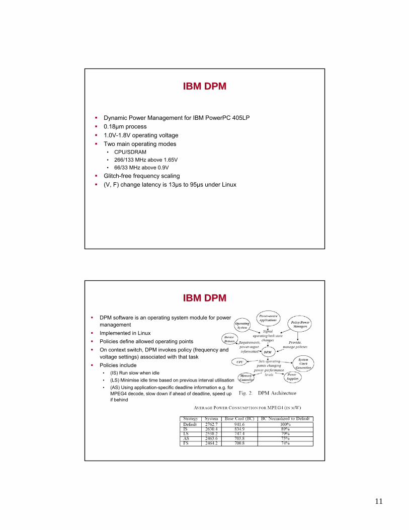
IBM DPMIBM DPM
Dynamic Power Management for IBM PowerPC 405LP0.18μm process1.0V-1.8V operating voltageTwo main operating modes
• CPU/SDRAM• 266/133 MHz above 1.65V• 66/33 MHz above 0.9V
Glitch-free frequency scaling(V, F) change latency is 13μs to 95μs under Linux
IBM DPMIBM DPM
DPM software is an operating system module for power managementImplemented in LinuxPolicies define allowed operating pointsOn context switch, DPM invokes policy (frequency and voltage settings) associated with that taskPolicies include
• (IS) Run slow when idle• (LS) Minimise idle time based on previous interval utilisation• (AS) Using application-specific deadline information e.g. for
MPEG4 decode, slow down if ahead of deadline, speed up if behind

12
Asynchronous = Low Power ? Handshake Asynchronous = Low Power ? Handshake Solutions HTSolutions HT--80C5180C51
8-bit microcontrollerCapable of operating in synchronous or asynchronous modeLow operational power consumptionZero stand-by power
• Assuming no leakageImmediate wake-upVery low electromagnetic emission (EME)
Synch vs. Synch vs. AsynchAsynch
Photon emission images of a clocked (left) and Handshake Technology (right) 80C51 microcontroller executing the same program. The red dots indicate the level and distribution of power dissipation, which is clearly lower and more localized in the HT-80C51.
Source: Handshake Solutions HT-80C51 Microcontroller

13
Synch vs. Synch vs. AsynchAsynch PowerPower
Asynchronous designs have not demonstrated intrinsic power advantages over synchronous processors…Au contraire!
Below is an example of a synchronous core for small size (60K gates) and power efficiency
ARM Cortex-M3
120 100 1.5 0.0015Worst case numbers in TSMC 180nm process
DMIPS MHz E / ins (pJ) mW / Mhz
Intelligent Energy Manager SWIntelligent Energy Manager SW
Automatically derive required performance level• Automatic monitoring to avoid missing deadlines• Sets frequency and voltage accordingly
Implemented as kernel modules for Linux• Only few kernel hooks are required• Autonomous from most of the kernel: portable
No application modifications required• But application-level power hints may be provided• Works with interactive applications
14
A utilization traceA utilization trace
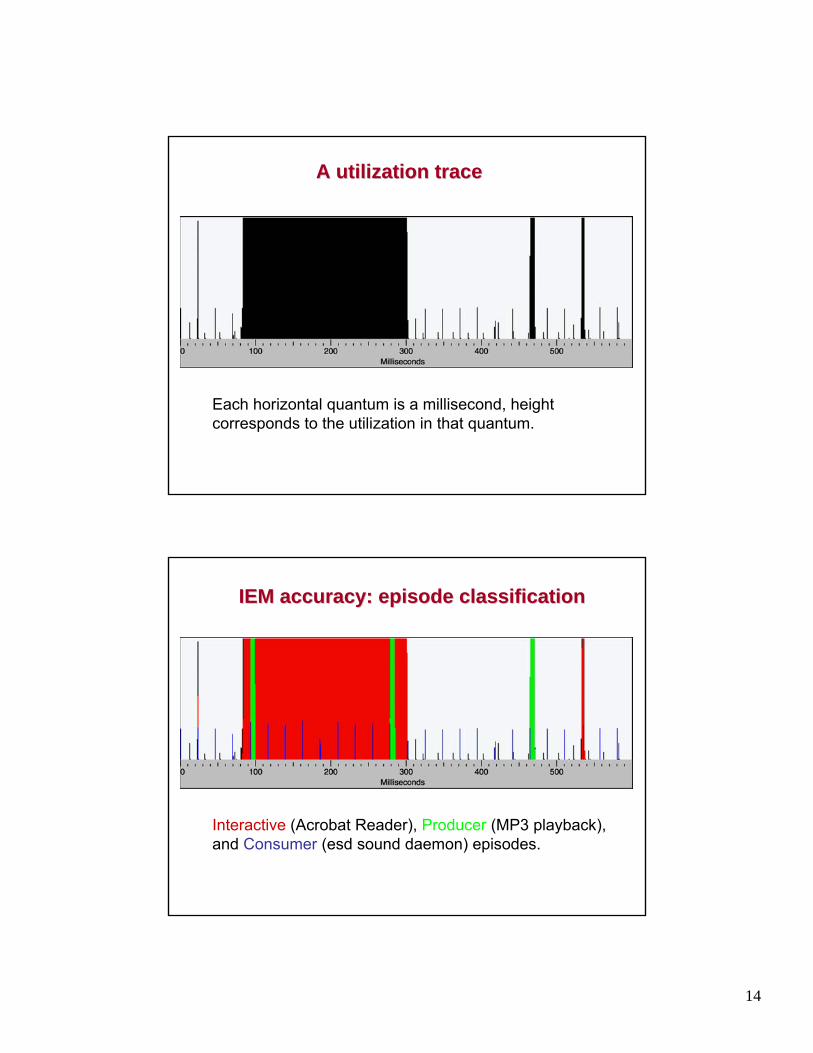
Each horizontal quantum is a millisecond, height corresponds to the utilization in that quantum.
IEM accuracy: episode classificationIEM accuracy: episode classification
Interactive (Acrobat Reader), Producer (MP3 playback), and Consumer (esd sound daemon) episodes.

15
Comparison with Comparison with LongRunLongRunSony PictureBook PCG-C1VN
• Transmeta Crusoe 5600 processor
Crusoe’s built-in LongRun policy used for comparisons.Implemented in Linux 2.4.4-ac18 kernel
600500400300
Frequency (Mhz)
TM5600 Frequency and voltage levels
1.61.41.351.3
Voltage (V)
0%36%53%67%
Power reduction
0%23%30%34%
Energy reduction
IEM vs. IEM vs. LongRunLongRun
LongRun: part of the processor firmware.• Interval based algorithm (guided by busy vs. idle time).• Min. and max. range is controllable in software.
IEM: implemented in OS kernel.• Multiple algorithms (perspectives / interactive).• Takes the quality of the user experience into account.
Comparisons on following graphs.• Repeated runs of interactive benchmarks are close but not identical.• Transitions to sleep are usually not shown.

16
No user activityNo user activity
Time (s)
Perf
orm
ance
leve
lPe
rfor
man
ce le
vel
Time (s)
LongRun
IEM
Frequency range of the TM5600 processor.
50% = 300Mhz @ 1.3V
100% = 600Mhz @ 1.6V
EmacsEmacs
Time (s)
Perf
orm
ance
leve
lPe
rfor
man
ce le
vel
Time (s)
LongRun
IEM

17
Acrobat ReaderAcrobat Reader
Time (s)
Perf
orm
ance
leve
lPe
rfor
man
cele
vel
Time (s)
LongRun
IEM
Acrobat Reader with sleep transitionsAcrobat Reader with sleep transitions
Time (s)
Perf
orm
ance
leve
lPe
rfor
man
cele
vel
Time (s)
LongRun
IEM
Frequent transitions to/from sleep mode. Longer durations without sleeping.

18
PlaympegPlaympeg: Red: Red’’s Nightmare (complete)s Nightmare (complete)
Time (s)
Perf
orm
ance
leve
lPe
rfor
man
cele
vel
Time (s)
LongRun
IEM
PlaympegPlaympeg: Red: Red’’s Nightmare (segment)s Nightmare (segment)
Time (s)
Perf
orm
ance
leve
lPe
rfor
man
cele
vel
LongRun
IEM
Time (s)
19
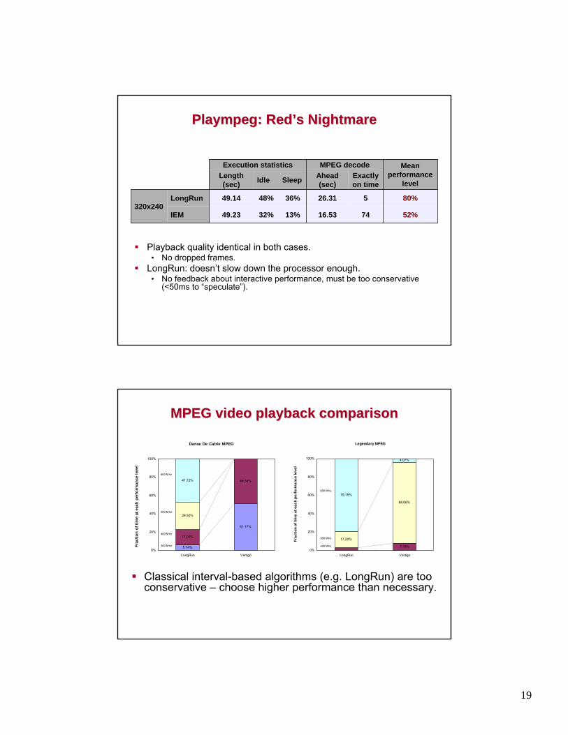
PlaympegPlaympeg: Red: Red’’s Nightmares Nightmare
Playback quality identical in both cases.• No dropped frames.
LongRun: doesn’t slow down the processor enough.• No feedback about interactive performance, must be too conservative
(<50ms to “speculate”).
52%7416.5313%32%49.23IEM
80%526.3136%48%49.14LongRun320x240
Exactly on time
Ahead (sec)SleepIdleLength
(sec)
Mean performance
level
MPEG decodeExecution statistics
MPEG video playback comparisonMPEG video playback comparison
Classical interval-based algorithms (e.g. LongRun) are too conservative – choose higher performance than necessary.
Legendary MPEG
17.20%
79.15%
7.78%
88.06%
4.07%
0%
20%
40%
60%
80%
100%
LongRun Vertigo
Frac
tion
of ti
me
at e
ach
perf
orm
ance
leve
l
400 M hz
500 M hz
600 M hz
Danse De Cable MPEG
5.74%
17.04%
29.50%
47.72%
51.17%
48.34%
0%
20%
40%
60%
80%
100%
LongRun Vertigo
Frac
tion
of ti
me
at e
ach
perfo
rman
ce le
vel
600 M hz
500 M hz
400 M hz
300 M hz

20
-1.2
-0.8
-0.4
0
0.4
0.8
1.2
0.1 5.1 10.1 15.1
Vbs
VddV
olta
ge (V
)Freq (GHz)
Optimal Vdd and Vbs vs. Frequency
Combining Threshold (ABB) Scaling with DVSCombining Threshold (ABB) Scaling with DVS
Bias voltage can be applied to body to change the thresold voltageFor a given frequency find optimum vdd, vbs combinationGraph shows this trade-off for projected 70nm technology
Energy used in an inverter chainEnergy used in an inverter chain
Energy consumed through 10 inverters (theory vs. Spice = 12.7% error)DVS+ABB: 54% better than DVS alone, 74% better than DFS
1.E-11
1.E-10
1.E-09
1.E-08
1.03.05.07.09.011.013.015.0Frequency (GHz)
Tota
l Ene
rgy
(log)
Freq ScalingDVS OnlyDVS and ABBSPICE
Energy Consumed for Various Low-Power Techniques vs. Frequency

21
Energy use on real workloads Energy use on real workloads -- 180nm180nm
Data based on 0.18um TSMC modelsPerformance scaling: 100% to 50% in 16% stepsDVS+ABB: average energy reduction of 23% over DVS
Normalized Energy Consumed for Various Energy Scaling Techniques
100.00
100.00
100.00
100.00
40.87
44.68
36.15
48.65
33.04
40.43
21.54
37.84
0 20 40 60 80 100
Xmms
Mpeg
Emacs
Os
Energy (%)
DVS and ABBDVS aloneNo Scaling
Energy use on real workloads Energy use on real workloads -- 70nm70nm
Normalized Energy Consumed for Various Energy Scaling Techniques with 100% -10% Frequency Scaling in 5% steps
100.00
100.00
100.00
100.00
23.08
37.84
22.00
31.09
12.92
28.83
4.20
15.97
0 20 40 60 80 100
Xmms
Mpeg
Emacs
Os
Energy (%)
DVS and ABBDVS aloneNo Scaling
Data based on projected 70nm processPerformance scaling: 100% to 10% in 5% stepsDVS+ABB: average energy reduction of 48% over DVS

22
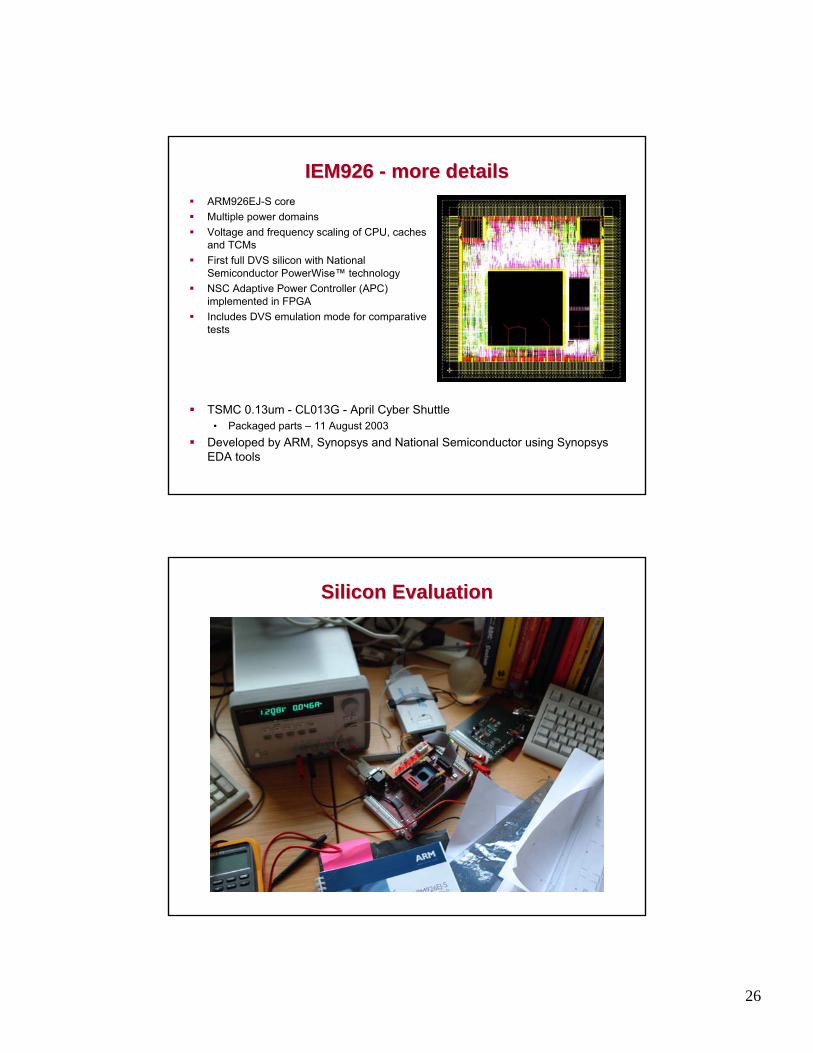
IEM926 on the benchIEM926 on the bench
IEM Test Chip Evaluation BoardIEM Test Chip Evaluation Board
Development board for IEM test chip to facilitate:• verification of SoC design• benchmarking of full system IEM performance

23
Technical SpecificationTechnical SpecificationDynamic Voltage Scaling methodology test vehicleARM926EJ-S core with retention-voltage TC RAMs4 dynamic performance levels supported in prototype• 240/180/120/60 MHz (+ 0 MHz stopped)
Pseudo-synchronous clock domains• Re-timed using latches (rather than fully asynchronous)• Interfaces synchronized to AMBA HCLK
Linux OS base porting peripheral setPrototype IEC with DVS emulation control modeFunctional Adaptive Voltage Scaling demonstrator• On-chip prototype PowerWise serial PSU interface• Off-chip FPGA control loop implementation
Core Voltage domainsCore Voltage domains
Dynamically scale voltage to both CPU and RAMs• But support state save to RAM and power-down of CPU
Level-shifter cells interface to always-powered SOC logic• Clamps hold signals low when domain voltage “unsafe”
CLAMP
ARM926EJ
L-SHIFT / C
LAM
P
L-SHIFT L-SHIFT
CLAMP
CPUCLK
Dynamic VoltageRAM with state
retention
Dynamic VoltageCPU with
power-down
CPURESET_NCACHERAMS
CACHERAMS
TCMTightly Coupled
Memories(TCMs)
VDDRAM
VDDCPU

24
Adaptive DVS supportAdaptive DVS support
Hardware performance monitor on CPU domain• Allow target clock frequency to determine voltage ‘headroom’• Support closed-loop power supply control
• Plus standard open-loop DVS
CLAMP
ARM926EJ
L-SHIFT / C
LAM
P
PerformanceMonitor
L-SHIFT L-SHIFT
CLAMP
L-SHIFT
CPUCLK
Dynamic VoltageRAM with state
retention
Dynamic VoltageCPU with
power-down
CPURESET_NCACHERAMS
CACHERAMS
TCMTCMSVDDRAM
VDDCPU
Clock latency issuesClock latency issues
CLAMP
ARM926EJ
L-SHIFT / C
LAM
P
PerformanceMonitor
L-SHIFT L-SHIFT
CLAMP
L-SHIFT
CPUCLK
Dynamic VoltageRAM with state
retention
Dynamic VoltageCPU with
power-down
CPURESET_NCACHERAMS
CACHERAMS
TCMTCMS
phi2LAT phi1LATHCLK
VDDRAM
VDDCPU
Individual System, CPU and RAM power domains• Level- shifters provide between SOC an CPU sub-system• CPU/RAM scaled together, or CPU off with RAM retained• IEM-ready cores will provide asynchronous bus interfaces

25
IEM test chip power domainsIEM test chip power domains
JTAGJTAG
Multi-ICE
SDRAM/
FLASH
TAP
ARM926EJS
16kByte
D-CACHE
16kByte
I-CACHE
16kByte
INSTR-SRAM
16kByte
DATA SRAM
PLL1
PLL2
Async. domain
CPU domain
Power, Test, Reset
& Clock control
APB
POWER MANAGER
Memory Controller
3-port Matrix
DMA
AHB/APB Bridge
DW_RTC
DW_INTC
DW_TIMER x2
DW_GPIO x 4
DW_UART x 22-port
Matrix
AHB_D
Sound
System bus domain
Async. domain
AHB BIU
Peripheral bus domain
AHB_I
AHB_S
CLAMP
ARM926EJ
phi2LAT phi1LAT
L-SHIFT / C
LAM
P
AMBA AHB/APB subsystem
PerformanceMonitor
NSCAPC
FPGAserializer
L-SHIFT L-SHIFT
CLAMP
PSU_VDDRAM
(0v7-1v2)
L-SHIFT
PCLKHCLK
HCLK
CPUCLK
CPUCLK
DynamicPerformance
Monitor
IEC
DynamicPerformance
Controller
DCG
Clock/Reset
APB INIT [N]
TARGETCLK
PERF
V_READY[N]
CPU_PERF
PLL(s)
PSU_VDDCPU
(0v7-1v2)
PSU_VDDSOC (1v2)
PSU_VDDPADS(3v3)
VBAT
SOC
Dynamic VoltageRAM with state
retention
Dynamic VoltageCPU with
power-down
PWIPowerWise Interface
CPURESET_N
CPURESET_NCACHERAMS
CACHERAMS
TCMTCMS
TARGETCLK
DBG /Multi-ICE
Synch
NSCAPC
AdaptivePower
ControllerFPGA
prototype
IEM926 IEM926 testchiptestchip
26
IEM926 IEM926 -- more detailsmore detailsARM926EJ-S coreMultiple power domainsVoltage and frequency scaling of CPU, caches and TCMsFirst full DVS silicon with National Semiconductor PowerWise™ technologyNSC Adaptive Power Controller (APC) implemented in FPGAIncludes DVS emulation mode for comparative tests
TSMC 0.13um - CL013G - April Cyber Shuttle• Packaged parts – 11 August 2003
Developed by ARM, Synopsys and National Semiconductor using SynopsysEDA tools
Silicon EvaluationSilicon Evaluation

27
IEM926 : Voltage Scaling AnalysisIEM926 : Voltage Scaling Analysis
Min voltage (room temp)Cached workload (Dhrystone)PLL settings:
• 300MHz• 288MHz• 276MHz• 264MHz• 252MHz• 240MHz• 228MHz• 216MHz
Vcpu vs CORECLK [Room Temp]
0.000
0.200
0.400
0.600
0.800
1.000
1.200
1.400
0 50 100 150 200 250 300 350
CORECLK (MHz)
Vcpu
(V)
100%
75% NOTE: 2x80%:1x66%50%25%
???
Core power vs CORECLK [Room Temp]
0.000
0.050
0.100
0.150
0.200
0.250
0.300
0 50 100 150 200 250 300 350
CORECLK (MHz)
Cor
e Po
wer
(W)
IEM926 : Power AnalysisIEM926 : Power Analysis
DFS only
Measured V/I (room temp)Cached workload (Dhrystone)PLL settings:
• 300MHz• 288MHz• 276MHz• 264MHz• 252MHz• 240MHz• 228MHz• 216MHz

28
IEM926 - Normalized Energy
0
0.2
0.4
0.6
0.8
1
1.2
0 50 100 150 200 250 300
Frequency (Mhz)
Ener
gy (r
elat
ive
to 1
.2V/
240M
Hz)
Energy @ limit + 20%Energy @ limit + 15%Energy @ limit + 10%Energy @ limit + 5%Energy @ limitEnergy at fixed 1.2V
IEM926 : Energy AnalysisIEM926 : Energy Analysis
Normalized to 1.2V nominal (room temp)PLL settings:• 240MHz
DFS only:• 1.2V nominal• No energy
savingsDVFS:• Limiting voltage• Effect of
+5,10,15,20% Vmargins
Questions?!Questions?!

1
Circuit and Circuit and MicroarchitecturalMicroarchitecturalTechniques Reducing OnTechniques Reducing On--Chip Chip
Cache Leakage Power Cache Leakage Power
Nam Sung KimNam Sung KimMicroprocessor Research, Intel Labs.Microprocessor Research, Intel Labs.
Intel Corp.Intel Corp.
OutlinesOutlinesTechnology and onTechnology and on--chip cache leakage trendschip cache leakage trends
Leakage reduction circuit techniquesLeakage reduction circuit techniques
MicroarchitecturalMicroarchitectural techniques for cache techniques for cache leakage power reductionleakage power reduction
Leakage optimization of multiLeakage optimization of multi--Level onLevel on--chip chip caches using multicaches using multi--VVTHTH assignmentassignment
Q & AQ & A

2
Technology and OnTechnology and On--Chip Cache Chip Cache Leakage Trends Leakage Trends
Dynamic and Leakage Power TrendsDynamic and Leakage Power Trends
ITRS 2002 projections with doubling # of transistors ITRS 2002 projections with doubling # of transistors every two yearsevery two years

3
OnOn--Chip Cache Leakage PowerChip Cache Leakage Power
Caches design with 70Caches design with 70--nm BPTM and subnm BPTM and sub--banking techniquebanking technique
leakage isleakage is57% of total cache power57% of total cache power
Rel
ativ
e Po
wer
OnOn--Chip Cache Leakage PowerChip Cache Leakage Power
Large and fast cachesLarge and fast caches•• Improving memory system performanceImproving memory system performance•• Consuming sizeable fraction of total chip powerConsuming sizeable fraction of total chip power
StrongARM StrongARM –– ~60% for on~60% for on--chip L1 cacheschip L1 caches
More caches integrated on chip More caches integrated on chip •• 2x64KB L1 / 1.5MB L2 in Alpha 214642x64KB L1 / 1.5MB L2 in Alpha 21464•• 256KB L2 / 3MB(6MB) L3 in Itanium 2256KB L2 / 3MB(6MB) L3 in Itanium 2
Increasing onIncreasing on--chip cache leakage powerchip cache leakage power•• Proportional to Proportional to exp (1/Vexp (1/VTHTH)) ×× # of bits# of bits•• 1MB L2 cache leakage power 1MB L2 cache leakage power –– 87% in 70nm tech87% in 70nm tech

4
Leakage Reduction Circuit Leakage Reduction Circuit TechniquesTechniques
66--Transistor SRAM Leakage Model Transistor SRAM Leakage Model
Two leakage paths via offTwo leakage paths via off--state devicesstate devices•• In storage cell In storage cell –– cell leakagecell leakage•• Connected to WL Connected to WL –– bitbit--line leakageline leakage
BL(1V)
BL(1V)
WL(0V)
WL(0V)
(0V) (1V)
off
off

5
IISNSN and and IISPSP for N and PMOS off devicesfor N and PMOS off devices
66--Transistor SRAM Leakage ModelTransistor SRAM Leakage Model
OffOff--state leakage current of inverterstate leakage current of inverter
( )DSq/kT
Vq/nkT
0Soff V1e1eIIDS
THV
λ+⎟⎟⎠
⎞⎜⎜⎝
⎛−⋅=
−−
Cell leakage currentCell leakage current•• Sum of two offSum of two off--state PMOS / NMOS currentstate PMOS / NMOS current
( ) ( )( ) ⎟⎟⎠
⎞⎜⎜⎝
⎛−+++=
−q/kT
V
DDPSPNSNSPSNLkg
DS
e1VIIIII λλ
Increasing VIncreasing VTHTH or voltage scaling reduces leakage or voltage scaling reduces leakage supersuper--linearlylinearly !!
MTCMOS PrinciplesMTCMOS Principles
Active modeActive mode•• LowLow--VVTHTH operationoperation
LowLow--VVTHTHPU/PD networkPU/PD network
HighHigh--VVTHTH
HighHigh--VVTHTH
Virtual Virtual VDDVDD
Virtual Virtual GNDGND
sleepsleep
sleepsleep
StandStand--by modeby mode•• Disconnect power supply Disconnect power supply •• through through highhigh--VVTHTH devicesdevices
Sleep devicesSleep devices•• GateGate--drive decreasedrive decrease•• Body effect increase VBody effect increase VTHTH
•• Ground bounceGround bounce
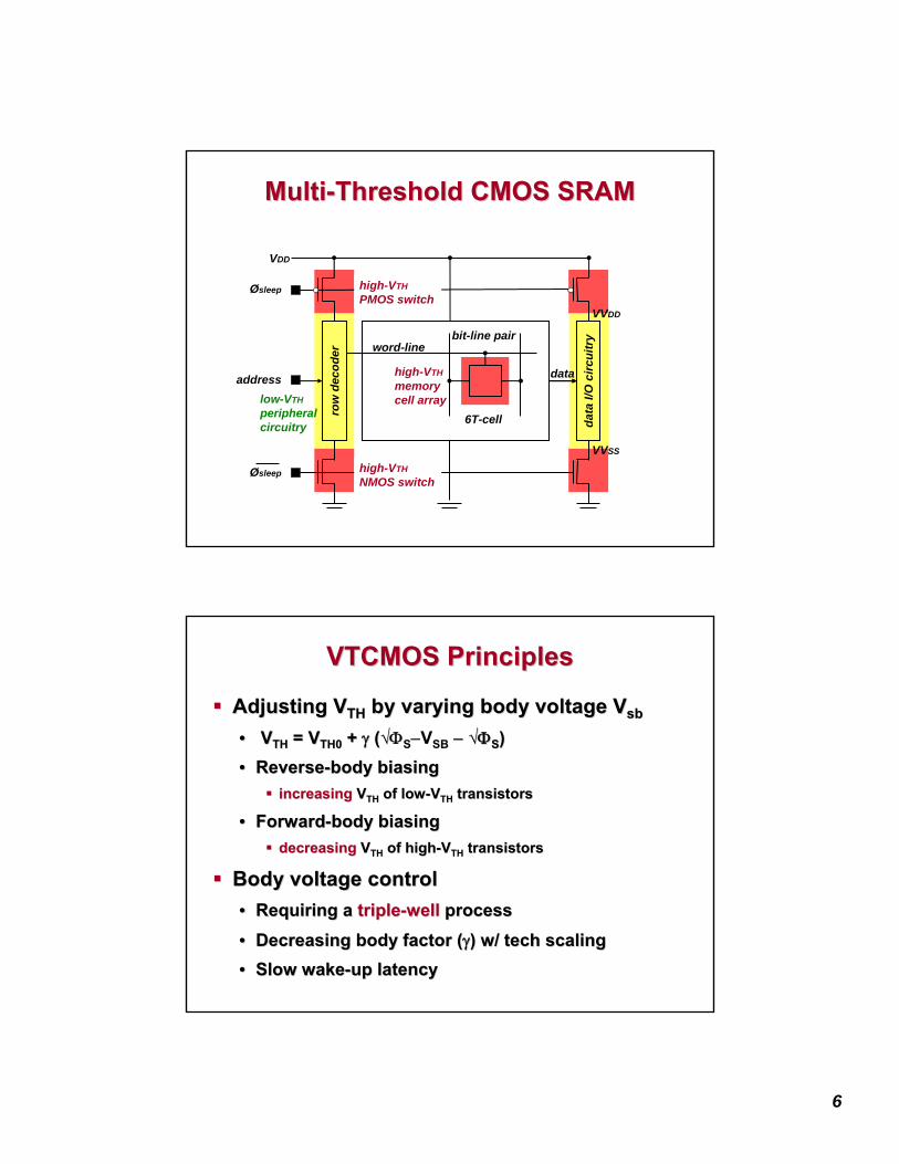
6
MultiMulti--Threshold CMOS SRAMThreshold CMOS SRAM
high-VTHmemorycell arraylow-VTH
peripheralcircuitry
row
dec
oder
6T-cell
word-linebit-line pair
Øsleep
address
VDD
VVDD
Øsleep
data
I/O
circ
uitr
y
data
VVSS
high-VTH PMOS switch
high-VTH NMOS switch
VTCMOS PrinciplesVTCMOS Principles
Adjusting VAdjusting VTHTH by varying body voltage by varying body voltage VVsbsb
•• VVTHTH = V= VTH0TH0 + + γγ ((√√ΦS−VSB −− √√ΦΦSS))•• ReverseReverse--body biasingbody biasing
increasingincreasing VVTHTH of lowof low--VVTHTH transistorstransistors
•• ForwardForward--body biasingbody biasingdecreasingdecreasing VVTHTH of highof high--VVTHTH transistorstransistors
Body voltage controlBody voltage control•• Requiring a Requiring a tripletriple--wellwell processprocess
•• Decreasing body factor (Decreasing body factor (γγ) w/ tech scaling) w/ tech scaling•• Slow wakeSlow wake--up latencyup latency

7
adaptive body biasing
circuitry
Adaptive Body Bias VTCMOS SRAMAdaptive Body Bias VTCMOS SRAMVDD+ (3.3)VDD (1.0)
VSS
VVSS
Øsleep
Øsleep
HH--VVTHTH
HH--VVTHTH
HH--VVTHTH
HH--VVTHTH
D1
D2
VD1
Vm
VD2
VVDD
Q2
Q1
Q3
Q4
BP
DualDual--VVTHTH CMOS PrinciplesCMOS Principles
Using Using •• LowLow-- / / highhigh--VVTHTH for critical / nonfor critical / non--critical pathscritical paths
Reducing both Reducing both activeactive and and standstand--byby leakage leakage powerpowerLeakage reductionLeakage reduction•• More effective than VTCMOS More effective than VTCMOS
decreasing body factor (decreasing body factor (γγ) w/ tech scaling) w/ tech scaling
•• For S = 85mV/decadeFor S = 85mV/decadereducing leakage by reducing leakage by ××1010 for each 85mV Vfor each 85mV VTHTH increaseincrease

8
DualDual--VVTHTH CMOS SRAMCMOS SRAM
UsingUsing•• LowLow--VVTHTH for peripheral circuit (e.g., decoders)for peripheral circuit (e.g., decoders)•• HighHigh--VVTHTH for memory cellsfor memory cells
Unavoidable to use of highUnavoidable to use of high--VVTHTH in critical path in critical path of memory cellof memory cell
H-VTH
BLH-VTH
H-VTH
BL BLBL
GatedGated--VVDDDD CMOS SRAMCMOS SRAM
MTCMOS variantMTCMOS variant•• Using highUsing high--VVTHTH devicedevice•• Destroying statesDestroying states•• ××10~10~ leakage reductionleakage reduction•• Access time impactAccess time impact
VDD
sleep
VVSS
VSS
Forced stacking variantForced stacking variant•• Using lowUsing low--VVTHTH devicedevice•• Preserving statePreserving state•• 40%40% leakage reductionleakage reduction•• Floated VVFloated VVSSSS –– noise issuenoise issue

9
VVDD
VSS
VDD VDD Low sleep
DVS CMOS SRAMDVS CMOS SRAM
Voltage ScalingVoltage Scaling•• Using VUsing VDDDD control devicescontrol devices•• Preserving statesPreserving states•• ××7~87~8 leakage reductionleakage reduction•• Fast wakeFast wake--upup•• No access time impactNo access time impact•• Stability and softStability and soft--errorerror•• issues during sleep timeissues during sleep time
read current pathread current path
sleep
Leakage Saving via Voltage ScalingLeakage Saving via Voltage Scaling
wowo/ BL leakage/ BL leakage
96% Reduction96% Reduction
w/ BL leakagew/ BL leakage
80% Reduction80% Reduction

10
Minimum StateMinimum State--Preserving VoltagePreserving Voltage
““00””
““11””
4T4T--storage storage cellcell
~80mV~80mV
““00””
““11””
6T6T--full full cellcell
~95mV~95mV
WakeWake--up Latency and Energyup Latency and Energylatencylatency
22--cycle wakecycle wake--upup
11--cycle wakecycle wake--upup
latencylatency
energyenergy
1.48% more area 1.48% more area for 64for 64××Lmin per 128Lmin per 128--bit linebit line

11
QQcritcrit
LkgLkg
Soft Error SusceptibilitySoft Error Susceptibility
s
criticalQ
Q
flux eCSNSER−
××∝
QQcritcrit decreases linearly decreases linearly w/ voltage scalingw/ voltage scaling
Leakage reduced Leakage reduced supersuper--linearlylinearly
SummarySummary
MTCMOSMTCMOS
VTCMOSVTCMOS
State preservingState preserving
GatedGated--VVDDDD
DVSDVS
DualDual--VVTHTH
ActiveActiveLeakageLeakage
StandStand--bybyLeakageLeakage
WakeWake--upupTimeTime
Access Access TimeTime
22
11
33
44
44
11
44
22
33
55
44
22
55
22
11
55
22
44
33
11
LowLow--Leakage SRAM Leakage SRAM CktCkt ComparisonsComparisons

12
MicroarchitecturalMicroarchitectural Techniques for Techniques for Cache Leakage Power Reduction Cache Leakage Power Reduction
Microarchitectural TechniquesMicroarchitectural Techniques
Incorporating w/ lowIncorporating w/ low--leakage leakage cktckt techniquestechniques•• GatedGated--VVDDDD, VTCMOS, MTCMOS, DVS, etc., VTCMOS, MTCMOS, DVS, etc.
Basic microarchitectural controlsBasic microarchitectural controls•• Exploiting generational cache access patternsExploiting generational cache access patterns•• Switching cache line powerSwitching cache line power--mode based on runmode based on run--
time decision from the access patternstime decision from the access patterns

13
Data Cache Working Set AnalysisData Cache Working Set Analysis
n=1 previous windown=1 previous window
n=2n=2
n=8n=8
n=32n=32
7%7%
16%16%
34%34%
8%8%
11%11%
12%12%8%8%
6%6%
5%5%16%16%
12%12% 12%12%
Inst Cache Working Set AnalysisInst Cache Working Set Analysis
n=1 previous windown=1 previous window
n=2n=2
n=8n=8
n=32n=32
4%4%
14%14%
3%3%
28%28%1%1%
21%21%
11%11%
3%3%18%18%
13%13%6%6% 9%9%

14
Gated VGated VDDDD--Based TechniquesBased Techniques
““Cache DecayCache Decay”” –– ISCA 2001ISCA 2001•• TurnTurn--off unused data cache lines using gatedoff unused data cache lines using gated--VVDDDD
unless accessed for a fixed interval unless accessed for a fixed interval requiring 2requiring 2--bit counter per line and 1 global counterbit counter per line and 1 global counter
““DRI CacheDRI Cache”” –– ISLPED 2000ISLPED 2000•• Resize cache size using gatedResize cache size using gated--VVDDDD based on based on
monitored miss statistics for a fix intervalmonitored miss statistics for a fix interval
Gated VGated VDDDD--Based TechniquesBased Techniques•• ProsPros
reducing reducing ××10~10~ leakage power for cache lines in standleakage power for cache lines in stand--by by modemodereducing some activereducing some active--mode leakage power due to mode leakage power due to stacking effectsstacking effects
•• ConsConsrequiring sophisticated prediction techniques to minimize requiring sophisticated prediction techniques to minimize the penalties incurred by accessing wrongfully turnedthe penalties incurred by accessing wrongfully turned--off off cache linescache linescausing excessive additional dynamic power / cyclescausing excessive additional dynamic power / cycles (in (in bigger L2 caches) for inappropriate sleep intervals bigger L2 caches) for inappropriate sleep intervals

15
DVSDVS--Based TechniquesBased Techniques
““Drowsy CachesDrowsy Caches”” –– ISCA 2002ISCA 2002•• Put all cache lines into statePut all cache lines into state--preserving sleep state preserving sleep state
using DVS and wakeusing DVS and wake--up lines onup lines on--demand demand requiring only 1 global counterrequiring only 1 global counter
•• ProsPros~6~6×× leakage power reduction leakage power reduction w/ small performance lossw/ small performance losssimple implementation w/ negligible access time impactsimple implementation w/ negligible access time impact
•• Cons.Cons.complicate complicate instrinstr. scheduling for OOO processors when . scheduling for OOO processors when accessing sleeping cache linesaccessing sleeping cache lines
Dual VDual VTHTH--Based TechniquesBased Techniques
Asymmetric DualAsymmetric Dual--VVTHTH CacheCache•• Optimizing leakage power of SRAM cell for storing Optimizing leakage power of SRAM cell for storing
““00”” using highusing high--VVTHTH devices in SRAM cellsdevices in SRAM cellsexploiting highly biased memory bits to exploiting highly biased memory bits to ““00”” in SPEC2Kin SPEC2Krequiring special senserequiring special sense--amplifier / slower access timeamplifier / slower access time
H-VTH
BL(1)
BL(1)
01

16
Gated BitGated Bit--line line PrechargePrecharge
Gated BitGated Bit--line line PrechargePrecharge
WL
BL BL
WL
gated clock signalclock
clock buffer
precharge

17
OnOn--Demand Demand PrechargePrecharge ((InstrInstr Cache)Cache)88××4KB sub4KB sub--banksbanks
44××8KB8KB
22××16KB16KB
Source of SubSource of Sub--Bank TransitionBank Transition
unconduncond
condcond
subsub--bank bank boundaryboundary
same setsame setdiff waydiff way

18
PredictionPrediction--Based TechniqueBased Technique
11 11 01 1
current sbank idx
predictor idx
101 11 1 1 1 1
block idxset idxtag
00 1nextsbank idx
128-
entr
y(1
-R/1
-W p
orts
)
deco
der
7e
GBP Accuracy vs. RunGBP Accuracy vs. Run--Time IncreaseTime Increase
nono--predpred
6464
1K1K
Configuration: 32-KB, 2-way, and 8-sbanksbit-line leakage reduction: 80%~Run-time increase w/ 1K predictor: 0.4%

19
TimeTime--Based Gating TechniqueBased Gating Technique
GatedGated--prechargeprecharge –– MICRO 2003MICRO 2003•• TurnTurn--off off prechargeprecharge devices of cache subdevices of cache sub--banks banks
unless accessed for a fixed time intervalunless accessed for a fixed time intervalaccessing 20% of 64KB subaccessing 20% of 64KB sub--banks banks in ~100 cycle windowin ~100 cycle window
prechargeCK signals
sbank-0
precharge signals
sbank-0sbank-0sbank-0
coun
ter
coun
ter
coun
ter
coun
ter
coun
ter
coun
ter
coun
ter
coun
ter
OnOn--Bank Fraction / RunBank Fraction / Run--Time IncreaseTime Increase
11
8832326464

20
SummarySummary
Combined architectural & Combined architectural & cktckt techniquestechniques•• Exploring temporal/spatial localities of L1 cache Exploring temporal/spatial localities of L1 cache
access patternsaccess patterns
•• TradeTrade--off among leakage reduction, access time, off among leakage reduction, access time, power management complexitypower management complexity
more aggressive leakage power reduction requiring more more aggressive leakage power reduction requiring more sophisticated architectural controls and causing more sophisticated architectural controls and causing more performance/power penalties when prediction wrongperformance/power penalties when prediction wrong
•• Reducing L1 cache leakage power by 6~10Reducing L1 cache leakage power by 6~10×× w/ w/ small avg. performance loss (~2%)small avg. performance loss (~2%)
Leakage Optimization of MultiLeakage Optimization of Multi--Level OnLevel On--Chip Caches using MultiChip Caches using Multi--
VVTHTH AssignmentAssignment

21
Cache Circuit ModelCache Circuit Model
Abus buffer w/ repeater
VTH1
VTH2
deco
der
Dbus buffer w/ repeater
VTH4
VTH3
sense-amp w/ I/O circuits
memory cell
word-line
bit-line paircache subcache sub--bank organizationbank organization
70nm Berkeley predictive 70nm Berkeley predictive technology modeltechnology model
Interconnect R/C annotatedInterconnect R/C annotated
repeaters used to minimize repeaters used to minimize interconnect delayinterconnect delay
Leakage Optimization via MultiLeakage Optimization via Multi--VVTHTH’’ss
Future Future nanoscalenanoscale CMOS technologyCMOS technology•• providing providing 2 or more V2 or more VTHTH’’ss for for leakage / speedleakage / speed
optimizationoptimization
QuestionsQuestions w/ more Vw/ more VTHTH choiceschoices•• assignment ofassignment of multimulti--VVTHTH’’ss for cachesfor caches•• tradetrade--off between leakage and speed of cachesoff between leakage and speed of caches•• costcost--effective number of Veffective number of VTHTH’’ss•• optimal L2 cache size considering optimal L2 cache size considering leakageleakage and and
avg. avg. memmem. access time. access time (AMAT)(AMAT) of processor of processor memory systemmemory system

22
Cache Access Time ModelCache Access Time Model
Decoder Decoder dealydealy
9x512 9x512 decdec
8x256 8x256 decdec7x128 7x128 decdec
∑=
=
−+=4i
1i
bi/Vi04TH3TH2TH1THdelay
THieBB)V,V,V,V(T
b/V0THdelay
THeBB)V(T +⋅+≈
MeasureMeasure circuit delay circuit delay at Vat VTHTH points using HSPICE points using HSPICE
Approx.Approx. circuit delay circuit delay using curve fitting using curve fitting
( )αTHDD
DDdelay VV
VLkT−⋅⋅
=
Cache Leakage Power ModelCache Leakage Power Model
∑=
=
−+=4i
1i
ai/Vi04TH3TH2TH1THleakage
THieAA)V,V,V,V(P
9x512 9x512 decdec
8x256 8x256 decdec
7x128 7x128 decdec
Decoder Leakage PowerDecoder Leakage Power
a/V0THleakage
THeAA)V(P −⋅+=
MeasureMeasure leakage power leakage power at Vat VTHTH points using HSPICE points using HSPICE
Approx.Approx. leakage power leakage power using curve fitting using curve fitting

23
Single Cache Leakage optimizationSingle Cache Leakage optimization
Leakage optimizationLeakage optimization
⎟⎟⎠
⎞⎜⎜⎝
⎛
++++= −−−− 44TH33TH22TH11TH a/V4
a/V3
a/V2
a/V10
4TH3TH2TH1THleakage
eAeAeAeAA
)V,V,V,V(Pmin
:objective
5.0V,...,V2.0eBeBeBeBB
)V,V,V,V(T:sconstraint
4TH1TH
b/V4
b/V3
b/V2
b/V10
4TH3TH2TH1THdelay target
44TH33TH22TH11TH
≤≤++++=
VVTHTH Assignment ApproachesAssignment Approaches
1 high V1 high VTH TH –– traditionaltraditional
Abus buffer w/ repeater
VTHL
VTHL
row
dec
oder
Dbus buffer w/ repeater
VTHL
VTHH
sense-amp w/ I/O circuits
memory cell
word-line
bit-line pair
1 high V1 high VTH TH –– a varianta variant
2 high V2 high VTHTH’’s s –– VVTHTH1 / V1 / VTHTH22
4 high V4 high VTHTH’’ss

24
VVTHTH Assignment ApproachesAssignment Approaches
1 high V1 high VTH TH –– traditionaltraditional
1 high V1 high VTH TH –– a varianta variant
2 high V2 high VTHTH’’s s –– VVTHTH1 / V1 / VTHTH22
4 high V4 high VTHTH’’ssAbus buffer w/ repeater
VTHH
VTHH
row
dec
oder
Dbus buffer w/ repeater
VTHH
VTHH
sense-amp w/ I/O circuits
memory cell
word-line
bit-line pair
VVTHTH Assignment ApproachesAssignment Approaches
1 high V1 high VTH TH –– traditionaltraditional
1 high V1 high VTH TH –– a varianta variant
2 high V2 high VTHTH’’s s –– VVTHTH1 / V1 / VTHTH22
4 high V4 high VTHTH’’ssAbus buffer w/ repeater
VTH1
VTH1
row
dec
oder
Dbus buffer w/ repeater
VTH1
VTH2
sense-amp w/ I/O circuits
memory cell
word-line
bit-line pair

25
VVTHTH Assignment ApproachesAssignment Approaches
1 high V1 high VTH TH –– traditionaltraditional
1 high V1 high VTH TH –– a varianta variant
2 high V2 high VTHTH’’s s –– VVTHTH1 / V1 / VTHTH22
4 high V4 high VTHTH’’ssAbus buffer w/ repeater
VTH1
VTH2
row
dec
oder
Dbus buffer w/ repeater
VTH4
VTH3
sense-amp w/ I/O circuits
memory cell
word-line
bit-line pair
Single Cache Leakage OptimizationSingle Cache Leakage Optimization
1 high1 high--VVTHTH –– traditionaltraditional
1 high1 high--VVTHTH –– variantvariant
2 high2 high--VVTHTH
VVTHTH’’s = 0.2Vs = 0.2V1MB L2 caches1MB L2 caches
80%80% leakage reduction w/ leakage reduction w/ 10%10% delay increasedelay increase
Peripheral circuits Peripheral circuits responsible ~responsible ~10%10% leakageleakage
More leakage reduction w/ More leakage reduction w/ more Vmore VTHTH

26
Optimized VOptimized VTHTH trendstrends
Memory cell array Memory cell array ––most most leakageleakage reductionreductionleast least delaydelay impactimpactmemory cellsmemory cells
decodersdecoders
Abus/Abus/DbusDbus
Decoders Decoders ––most most delaydelay impactimpactleast least leakageleakage reductionreduction
4 high4 high--VVTHTH schemescheme
Optimizing L2 leakage at fixed L1 sizeOptimizing L2 leakage at fixed L1 size
256KB256KB
512KB512KB
128KB128KB
Constraint Constraint –– maintaining maintaining the same the same AMATAMAT
Optimization Optimization –– use larger use larger but less leaky L2 cachesbut less leaky L2 caches
69%69%
85%85%
based on fast 16KB L1 based on fast 16KB L1

27
L2 Leakage saving at fixed L1 sizeL2 Leakage saving at fixed L1 size
100%100% 100%100% 100%100%
31.3%31.3%
10.9%10.9%0.7%0.7%
14.5%14.5%
0.4%0.4%
16KB16KB
128K
B12
8KB
256K
B25
6KB
512K
B51
2KB
32KB32KB
256K
B25
6KB
512K
B51
2KB
1024
KB
1024
KB
64KB64KB
512K
B51
2KB
1024
KB
1024
KB
L1 sizeL1 size
L2 sizeL2 size
Nor
mal
ized
leak
age
Nor
mal
ized
leak
age
SummarySummary
CostCost-- effective # of Veffective # of VTHTH for cache leakage for cache leakage reductionreduction•• Depending on the target access time, but Depending on the target access time, but 11 or or 2 2
extra high Vextra high VTHTH’’s is enough for leakage reductions is enough for leakage reduction•• 80%leakage reduction w/ 10% access time increase80%leakage reduction w/ 10% access time increase
L2 Cache leakageL2 Cache leakage•• Another Another design constraintdesign constraint in processor designin processor design•• TradeTrade--off among delay / area /off among delay / area / leakageleakage•• Small overall performance impact w/ slower but Small overall performance impact w/ slower but
less leaky L2 cachesless leaky L2 caches•• Larger but slower L2 caches at a fixed performanceLarger but slower L2 caches at a fixed performance

28
Q & AQ & A

1
Physical Basis of Variability in Physical Basis of Variability in Modern ICsModern ICs
Dennis SylvesterDennis SylvesterUniversity of MichiganUniversity of Michigan
Some slides courtesy: Nagib Hakim Some slides courtesy: Nagib Hakim (Intel), Kerry Bernstein (IBM), Andrew (Intel), Kerry Bernstein (IBM), Andrew
Kahng (UCSD), David Blaauw (UM)Kahng (UCSD), David Blaauw (UM)
OutlineOutlineDefinitions (classes) of variabilityDefinitions (classes) of variability•• Intra vs. interIntra vs. inter--die, systematic vs. random, impact of each, die, systematic vs. random, impact of each,
functional vs. parametric yieldfunctional vs. parametric yieldVariability sourcesVariability sources•• Critical dimensions (CD)Critical dimensions (CD)•• VthVth fluctuationsfluctuations•• Capacitive couplingCapacitive coupling•• Environmental: Power supply noise, temperature, etc.Environmental: Power supply noise, temperature, etc.
Single event upsets (soft errors)Single event upsets (soft errors)•• Definitions, trends, some simple techniques to combatDefinitions, trends, some simple techniques to combat
Goal: Take you to the last section of the tutorial where Goal: Take you to the last section of the tutorial where Todd will describe robust design techniques to cope Todd will describe robust design techniques to cope with all of thiswith all of this
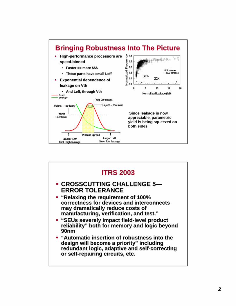
2
Bringing Robustness Into The PictureBringing Robustness Into The PictureHighHigh--performance processors are performance processors are speedspeed--binnedbinned•• Faster == more $$$Faster == more $$$
•• These parts have small These parts have small LeffLeff
Exponential dependence of Exponential dependence of leakage on leakage on VthVth•• And And LeffLeff, through , through VthVth
Process SpreadSmaller Leff
Fast, high leakageLarger Leff
Slow, low leakage
Freq Constraint
Reject – too slow
Power Constraint
Reject – too leaky
DelayLeakage
Process SpreadSmaller Leff
Fast, high leakageLarger Leff
Slow, low leakage
Freq Constraint
Reject – too slow
Power Constraint
Reject – too leaky
DelayLeakage
Since leakage is now appreciable, parametric yield is being squeezed on both sides
ITRS 2003ITRS 2003CROSSCUTTING CHALLENGE 5CROSSCUTTING CHALLENGE 5——ERROR TOLERANCEERROR TOLERANCE““Relaxing the requirement of 100% Relaxing the requirement of 100% correctness for devices and interconnects correctness for devices and interconnects may dramatically reduce costs of may dramatically reduce costs of manufacturing, verification, and test.manufacturing, verification, and test.””““SEUsSEUs severely impact fieldseverely impact field--level product level product reliabilityreliability”” both for memory and logic beyond both for memory and logic beyond 90nm90nm““Automatic insertion of robustness into the Automatic insertion of robustness into the design will become a prioritydesign will become a priority”” including including redundant logic, adaptive and selfredundant logic, adaptive and self--correcting correcting or selfor self--repairing circuits, etc.repairing circuits, etc.

3
Printing in the Printing in the SubwavelengthSubwavelength RegimeRegime
0.25µ 0.18µ
0.13µ 90-nm 65-nm
Layout
Figures courtesy Synopsys Inc.
Variation: Across-Wafer Frequency
Figure courtesy S. Nassif, IBM

4
0%
20%
40%
60%
80%
100%
Intel IBM Synopsys TUE-Magma
Cadence STMicro
Variability/Litho/Mask/Fab Low Power/LeakagePower Delivery/Integrity Tool/Flow Enhancements/OAIP Reuse/Abstraction/SysLevel Design DSM AnalysisP&R and Opt Others (Lotto)
DACDAC--2003 Nanometer Futures Panel:2003 Nanometer Futures Panel:Where should extra design automation R&D $ be spent?Where should extra design automation R&D $ be spent?
Fig source: A.B. Kahng
Robustness vs. LowRobustness vs. Low--PowerPowerPower is reduced by slowing Power is reduced by slowing nonnon--critical paths (exploiting critical paths (exploiting slack)slack)When power reduction is highly When power reduction is highly effective (good), many paths effective (good), many paths become critical (bad)become critical (bad)•• Implies difficulty in timing Implies difficulty in timing
verification and optimizationverification and optimization•• Parametric yield reductionParametric yield reduction
delay
- - - - - - - - - - - - - - -
# of
pat
hs
Critical path delay
delay
- - - - - - - - - - - - - - -
# of
pat
hs
POWER OPTIMIZATION

5
Robustness vs. LowRobustness vs. Low--Power, 2Power, 2VVdddd reduction yields reduction yields quadratic dynamic power quadratic dynamic power reductions + marked leakage reductions + marked leakage improvementimprovementBut: enhances susceptibility But: enhances susceptibility to single event upsets (to single event upsets (SEUsSEUs) ) due to charge reductiondue to charge reduction
Robust design practices Robust design practices include redundancy, include redundancy, widening devices/wires to widening devices/wires to limit variabilitylimit variability•• Larger total capacitance, Larger total capacitance,
powerpower
MotivationMotivation
Concurrent technology and design development.Concurrent technology and design development.•• Surprises are the normSurprises are the norm•• Issues are identified lateIssues are identified late
NonNon--uniformity and uncertainty are having increased impactuniformity and uncertainty are having increased impact•• PowerPower•• PerformancePerformance
•• ReliabilityReliability•• CostCost
Possible solutions:Possible solutions:•• Process: e.g. performance/control tradeoff Process: e.g. performance/control tradeoff •• Design: e.g. robustness/area (power) tradeoffDesign: e.g. robustness/area (power) tradeoff•• Modeling and CAD improvements: Shift from uncertainty to modeledModeling and CAD improvements: Shift from uncertainty to modeled
nonnon--uniformity.uniformity.
Courtesy N. Hakim (Intel)

6
Sources of Uncertainty in DesignSources of Uncertainty in Design
OperationApplied signalsPower supply voltageOn chip voltageSelf heatingDevice degradationetc.
Design modelApproximations Estimation errors in model assumptions Changing reqs, etc.
Manufacturing and packagingProcess change and driftSystematic variationUnassignable causesetc.
Courtesy N. Hakim (Intel)
Limiting Factors in Modeling Limiting Factors in Modeling UncertaintyUncertainty
Concurrency between process and product development Concurrency between process and product development •• Many systematic effects cannot be modeled Many systematic effects cannot be modeled
Requires additional knowledge about the design/process.Requires additional knowledge about the design/process.•• Impact mitigated through design rules and other collateralImpact mitigated through design rules and other collateral
Sequential and iterative nature of designSequential and iterative nature of design•• Limits available information for better modelingLimits available information for better modeling
E.g. placement, layout, etc.E.g. placement, layout, etc.Design Methodology and Tools:Design Methodology and Tools:•• Design efficiency: Design efficiency:
Mitigating uncertainty requires additional design efforts, or a Mitigating uncertainty requires additional design efforts, or a change change in methodologyin methodology
•• Established practices evolve slowlyEstablished practices evolve slowlyRequires tools, global perspective, added riskRequires tools, global perspective, added risk
Solution must attack problem at all 3 levels:Solution must attack problem at all 3 levels:•• More interactive process/product developmentMore interactive process/product development•• TopTop--down design approachdown design approach•• Tools and methodologies for a practical way to account for uncerTools and methodologies for a practical way to account for uncertainty in tainty in
designdesignCourtesy N. Hakim (Intel)

7
Types of VariationTypes of VariationRandomRandom•• Modeling consists of approximating the random effect Modeling consists of approximating the random effect
by a normal distributionby a normal distribution•• Knowing mean and Knowing mean and σσ, use statistical approaches (Monte , use statistical approaches (Monte
Carlo, worstCarlo, worst--case) to accountcase) to account•• Example: random Example: random dopantdopant fluctuations which impact fluctuations which impact
device device VVthth
SystematicSystematic•• This type of effect should be studied and modeled This type of effect should be studied and modeled
deterministically to allow for deterministically to allow for design with variationdesign with variation in in mindmind
•• Includes environmental variations such as IR drop, Includes environmental variations such as IR drop, thermal gradients, crosstalk noisethermal gradients, crosstalk noise--onon--delay effectsdelay effects
More Categories of VariationMore Categories of Variation
InterInter--die (diedie (die--toto--die, D2D)die, D2D)•• Across the wafer or between wafersAcross the wafer or between wafers•• Larger length scale (~8 inch) gives rise to larger Larger length scale (~8 inch) gives rise to larger
potential processpotential process--induced variationinduced variation•• Example: Thermal gradient in furnace leads to variation Example: Thermal gradient in furnace leads to variation
in in TToxox across the waferacross the waferIntraIntra--die (withindie (within--die, WID)die, WID)•• Each device on the chip is affected differentlyEach device on the chip is affected differently•• Length scale (typically mm), magnitude of variation is Length scale (typically mm), magnitude of variation is
often smaller than interoften smaller than inter--diedie•• But impact of variation can be greater!But impact of variation can be greater!•• Example: Proximity effects where minimum pitch Example: Proximity effects where minimum pitch
features exhibit different width bias than isolated features exhibit different width bias than isolated featuresfeatures

8
InterInter--die vs. Intradie vs. Intra--die Variationdie Variation
InterInter--die variation is not always larger than intradie variation is not always larger than intra--die die (ILD)(ILD)
Uncertainty or NonUncertainty or Non--UniformityUniformity
Uncertainty
Random variations Systematic effects
Non-uniformity
Modeleddeterministically?
Y
N
Systematiceffect
uncertainty
Random effects Random effectsNon-uniformity
Modeling non-uniformities allows reducing the uncertainty interval
Courtesy N. Hakim (Intel)
9
YieldYieldFunctionalFunctional•• Chip doesnChip doesn’’t workt work•• Short and open circuits in metal levels, pinholes in gate Short and open circuits in metal levels, pinholes in gate
oxideoxide•• ElectromigrationElectromigration failure (timefailure (time--dependent)dependent)
ParametricParametric•• Chips run at different speedsChips run at different speeds•• Binning of parts, sell at different prices if possibleBinning of parts, sell at different prices if possible•• Crosstalk noise, ILD variation, Crosstalk noise, ILD variation, IIdsatdsat variation (variation (LLeffeff, , TToxox, , VVthth))
Parametric yield loss has become dominant over Parametric yield loss has become dominant over defectdefect--based yield loss as processing conditions based yield loss as processing conditions improvedimprovedWe are concerned with parametric effects in this We are concerned with parametric effects in this discussiondiscussion
OutlineOutline
Definitions (classes) of variabilityDefinitions (classes) of variability
Variability sourcesVariability sources•• Critical dimensions (CD)Critical dimensions (CD)•• VthVth fluctuationsfluctuations•• Capacitive couplingCapacitive coupling•• Environmental: Power supply noise, temperature, Environmental: Power supply noise, temperature,
etc.etc.
Single event upsets (soft errors)Single event upsets (soft errors)

10
Main Sources of Process VariationsMain Sources of Process Variations
CD variationCD variation•• Systematic and random dieSystematic and random die--toto--die and withindie and within--die die
sources sources
Width variationWidth variation•• Impact on narrow transistorsImpact on narrow transistors
VthVth fluctuationsfluctuations•• Most impact on short, narrow devicesMost impact on short, narrow devices
InterconnectInterconnect•• Pattern density effects from polishing, dishingPattern density effects from polishing, dishing
Courtesy N. Hakim (Intel)
Decomposition of CD Variation Decomposition of CD Variation PatternsPatterns
-150 -100 -50 0 50 100 150
-150
-100
-50
050
100
-150 -100 -50 0 50 100 150
-150
-100
-50
050
100
-150 -100 -50 0 50 100 150
-150
-100
-50
050
100
-150 -100 -50 0 50 100 150
-150
-100
-50
050
100
Total CD Variation Random component
Within-Die component Within Wafer component
Courtesy N. Hakim (Intel)

11
Sources of CD UncertaintiesSources of CD UncertaintiesDieDie--toto--die variationdie variation•• From wafer nonFrom wafer non--uniformityuniformity
Long range withinLong range within--die die variationvariation•• Stepper nonStepper non--uniformity, lens uniformity, lens
aberration, flareaberration, flare•• Density nonDensity non--uniformityuniformity
ShortShort--range WID variationrange WID variation•• From patterning limitations, From patterning limitations,
mask alignment, line edge mask alignment, line edge roughness, etc.roughness, etc.
-14.
7
-8.4
-2.1 4.2
10.5
-9.9
-4.95
0
4.95
9.9
Across scan location (mm)
Across lens location
(mm
)
1 2
Courtesy N. Hakim (Intel)
Modeling Poly CD WID VariationModeling Poly CD WID VariationLongLong--range WID CD variationrange WID CD variation•• CD variation between two devices separated by a distance d can bCD variation between two devices separated by a distance d can be e
modeled by a spatial correlation function such as:modeled by a spatial correlation function such as:
•• Where Where Var(CDVar(CD) is the total CD variance of a single device, and dl is a ) is the total CD variance of a single device, and dl is a characteristic distance for a particular technology.characteristic distance for a particular technology.
Affects large circuits (> 1mm spread)Affects large circuits (> 1mm spread)ShortShort--range variationrange variation•• May have a deterministic component from proximityMay have a deterministic component from proximity•• Generally modeled as a random component. Generally modeled as a random component. •• MultiMulti--fingered devices see statistical averaging of the random fingered devices see statistical averaging of the random
component for Icomponent for Idd, less clear for , less clear for IIoffoff
Averages out quickly for several gates deep pathsAverages out quickly for several gates deep pathsAffects matched pairs, reference circuits, etc.Affects matched pairs, reference circuits, etc.
⎟⎠⎞
⎜⎝⎛ −
−Δ )exp(1)(2~)(dldCDVarCDVar d
legsCDVarCDVar glemult /#)()( sin=
Courtesy N. Hakim (Intel)

12
Sources of Width VariationSources of Width VariationLithography sources:Lithography sources:•• Poly and diffusion Poly and diffusion
roundingrounding•• Compounded by mask Compounded by mask
alignmentalignment
Polishing:Polishing:•• Unequal polish of Unequal polish of SiSi
and STI materialand STI material•• Density dependentDensity dependent•• Impacts both IImpacts both Idd and and
CCgategate
Z
Poly
Diffusion
Courtesy N. Hakim (Intel)
Impact and Mitigation of Width Impact and Mitigation of Width VariationVariation
Circuit impactCircuit impact•• Width variation affects both Width variation affects both IIdsatdsat / / RRdsds and and CCgategate
•• Affects only narrow devices:Affects only narrow devices:Analog circuits, SRAM, register files, standard cells, Analog circuits, SRAM, register files, standard cells,
Mitigation by:Mitigation by:•• GuardbandingGuardbanding•• Layout and density design rules Layout and density design rules
But may also unnecessarily impact large devices But may also unnecessarily impact large devices
•• Device matching design rulesDevice matching design rules
Courtesy N. Hakim (Intel)

13
VthVth Variation SourcesVariation SourcesDieDie--toto--diedie•• From wafer level uniformity (From wafer level uniformity (ToxTox, Implantation, etc), Implantation, etc)
Random WID component (dominant)Random WID component (dominant)•• Random Channel Random Channel DopantDopant Fluctuations f(W, L)Fluctuations f(W, L)•• Random Poly Random Poly DopantDopant FluctuationsFluctuations•• Random Fixed Oxide ChargeRandom Fixed Oxide Charge
Strong device size dependencyStrong device size dependency
sigma(ΔVt) versus technology generation(for minimum sized device)
180nm 130nm 90nm 70nm
Technology generation
sigm
a(Δ
Vtn)
(mV)
Are
a ( μ
m^2
) sig(VTN) (Cert)n: Ze*Le (Cert)
Courtesy N. Hakim (Intel)
Random Dopant Fluctuations, IntelRandom Dopant Fluctuations, Intel’’s Views View
10
100
1000
10000
1000 500 250 130 65 32
Technology Node (nm)
Mea
n N
umbe
r of D
opan
t Ato
ms
UniformUniform NonNon--uniformuniform
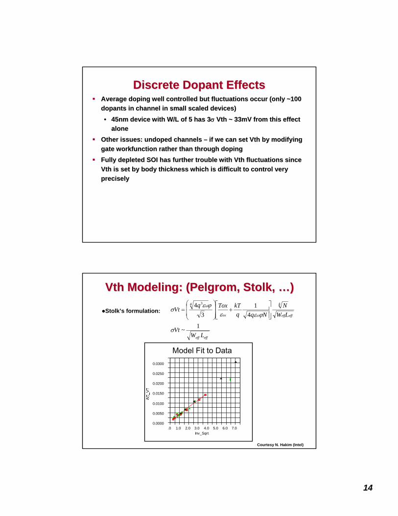
14
Discrete Discrete DopantDopant EffectsEffectsAverage doping well controlled but fluctuations occur (only ~100Average doping well controlled but fluctuations occur (only ~100dopantsdopants in channel in small scaled devices)in channel in small scaled devices)•• 45nm device with W/L of 5 has 345nm device with W/L of 5 has 3σσ VthVth ~ 33mV from this effect ~ 33mV from this effect
alonealoneOther issues: Other issues: undopedundoped channels channels –– if we can set if we can set VthVth by modifying by modifying gate gate workfunctionworkfunction rather than through dopingrather than through dopingFully depleted SOI has further trouble with Fully depleted SOI has further trouble with VthVth fluctuations since fluctuations since VthVth is set by body thickness which is difficult to control very is set by body thickness which is difficult to control very preciselyprecisely
VthVth Modeling: (Modeling: (PelgromPelgrom, , StolkStolk, , ……))
effeff
effeffsiox
si
LWVt
LWN
NqqkTToxq
Vt
1~
41
34 44 3
σ
ϕεεϕε
σ⎥⎥⎦
⎤
⎢⎢⎣
⎡+
⎟⎟
⎠
⎞
⎜⎜
⎝
⎛=Stolk’s formulation:
0.0000
0.0050
0.0100
0.0150
0.0200
0.0250
0.0300
.0 1.0 2.0 3.0 4.0 5.0 6.0 7.0Inv_Sqrt
Model Fit to Data
Courtesy N. Hakim (Intel)

15
Impact and MitigationImpact and Mitigation
Largest impact is on analog circuits, memories, Largest impact is on analog circuits, memories, bandgapbandgap referencesreferences•• Impacts ability to match devicesImpacts ability to match devices•• Cannot be reduced by layout design rulesCannot be reduced by layout design rules
Impact on delay averages out for long pathsImpact on delay averages out for long paths
Mitigation by device engineeringMitigation by device engineering•• Graded wellsGraded wells•• Tip engineeringTip engineering
Mitigation by device upsizingMitigation by device upsizing•• Impact on cell areaImpact on cell area
Courtesy N. Hakim (Intel)
InterconnectInterconnect--Induced VariationsInduced Variations
Variation is systematic and depends on neighboring layout:1- Layout, Proximity2- Density
Sources:Metal Thickness: Etch (density), Polish (density, width)Dielectric: Etch (density)Metal width/spacing: Litho (proximity), etchVias: Lithography, dielectric thickness
txtr
tstg
tint
Repeater circuit
Courtesy N. Hakim (Intel)

16
CMP & Area FillCMP & Area Fill
wafer carrier silicon wafer
polishing pad
polishing table
slurry feeder
slurry
ChemicalChemical--Mechanical Planarization (CMP)Mechanical Planarization (CMP)Polishing pad wear, slurry composition, pad elasticity make Polishing pad wear, slurry composition, pad elasticity make this a very difficult process stepthis a very difficult process step
Pattern density effects result Pattern density effects result where dense and sparse where dense and sparse regions have very different regions have very different dielectric thicknessesdielectric thicknesses
Systematic & predictableSystematic & predictable
Coping with Pattern Density EffectsCoping with Pattern Density Effects
ILD thickness variation
• (Simple) function of underlying pattern density
Metal fill helps but today’s approaches are not smart
Cap impact not considered, chips come out running up to 20% slower than expectedFigs: Mehrotra, Nakagawa
Area fill feature insertionArea fill feature insertionDecreases local density variation and hence decreases the Decreases local density variation and hence decreases the ILD thickness variation after CMP ILD thickness variation after CMP
Post-CMP ILD thicknessFeatures
Area fillfeatures

17
Crosstalk Noise Impact on DelayCrosstalk Noise Impact on Delay
Cc
Goes by many names:Goes by many names:
Dynamic delay, delay Dynamic delay, delay degradation/deterioration, noisedegradation/deterioration, noise--onon--delaydelay
-- Impact of neighboring signal activity Impact of neighboring signal activity on switching delayon switching delay
-- NNeighboring lines switch in opposite eighboring lines switch in opposite direction of victim line, delay increasesdirection of victim line, delay increases
Miller EffectMiller Effect
-- Both terminals of capacitor are Both terminals of capacitor are switched in opposite directions (0 switched in opposite directions (0 VddVdd, , VddVdd 0)0)
-- Effective voltage is doubled, additional Effective voltage is doubled, additional charge is needed (Q=CV) [simplified charge is needed (Q=CV) [simplified model]model]
Impact of neighboring signal Impact of neighboring signal activityactivity
Intel 1GHz Intel 1GHz CoppermineCoppermine –– 50MHz drop in timing 50MHz drop in timing due to capacitive crosstalk effectsdue to capacitive crosstalk effects
Ref: Intel, ISSCC00

18
Noise Immune Layout FabricNoise Immune Layout Fabric
This layout style This layout style trades off trades off areaarea for:for:•• Noise immunity Noise immunity (both C and L)(both C and L)
•• Minimizes Minimizes variations (CMP)variations (CMP)
•• PredictablePredictable
•• Easy layoutEasy layout
•• Simplifies power Simplifies power distributiondistribution
Ref: Khatri, DAC99
Major area penalty (>60%)
Impact of Interconnect VariationsImpact of Interconnect VariationsImpact on circuit delay depends on:Impact on circuit delay depends on:
11-- Driver / receiver sizingDriver / receiver sizing22-- Interconnect length: density uniformity Interconnect length: density uniformity
Need to consider both device and interconnect variationNeed to consider both device and interconnect variationNeed to simulate multiple segments to assess overall Need to simulate multiple segments to assess overall impactimpactIC variation dominates long lines, device dominate short IC variation dominates long lines, device dominate short onesones
86%86%34%34%2%2%XtrXtr%%
14%14%66%66%98%98%IC%IC%
33%33%66%66%100%100%
IC length IC length (% of max repeater (% of max repeater
length)length)
Relative impact of interconnect and transistor variationsRelative impact of interconnect and transistor variationsImpact expressed as % of total varianceImpact expressed as % of total variance
Courtesy N. Hakim (Intel)

19
Interconnect Reliability ScalingInterconnect Reliability ScalingNew lowNew low--k materials have worse thermal properties than k materials have worse thermal properties than SiOSiO22Global wiring is more susceptible to thermal effects (selfGlobal wiring is more susceptible to thermal effects (self--heating) due to larger separation from substrateheating) due to larger separation from substratePolyimidesPolyimides yield ~30% lower allowable current density in yield ~30% lower allowable current density in 0.1 0.1 μμm global wiringm global wiringSelfSelf--heating effects lead to worsened heating effects lead to worsened electromigrationelectromigrationreliability (reliability (even in Cueven in Cu) since the metal temperature is ) since the metal temperature is increased over the local ambient temperatureincreased over the local ambient temperature
Ref: Banerjee, DAC99
Table gives max. Table gives max. allowable peak allowable peak current density current density (MA/cm(MA/cm22))
Power distribution challengesPower distribution challengesPower distribution requires low IR drop and L*Power distribution requires low IR drop and L*di/dtdi/dtnoise across the dienoise across the die•• Supply currents and current transients get much worse with Supply currents and current transients get much worse with
scalingscalingPentium 3 power density distribution shownPentium 3 power density distribution shown•• Hot spots require more aggressive power grid topologiesHot spots require more aggressive power grid topologies•• Memory stays cool, integer execution units run hotMemory stays cool, integer execution units run hot•• Peak power density ~ 4Peak power density ~ 4--8X 8X
uniform densityuniform density
Ref: Pollack, Intel

20
Temperature Variation EffectsTemperature Variation EffectsVariation:Variation:•• Placement / program dependentPlacement / program dependent•• Varies slowly across the die, with a gradient of possibly Varies slowly across the die, with a gradient of possibly
several degrees per mmseveral degrees per mm•• Some correlation with IR drop in power gridSome correlation with IR drop in power grid
Variation Effects:Variation Effects:•• Device onDevice on--current; speedcurrent; speed•• Interconnect resistance Interconnect resistance •• Leakage (exponential)Leakage (exponential)•• Strong impact on reliability Strong impact on reliability
(EM)(EM)Impact doubles for each Impact doubles for each 5 degree increase5 degree increase
Common mode (e.g. global droop):Common mode (e.g. global droop):•• E.g. from largeE.g. from large--scale L scale L dI/dtdI/dt•• Path delay Path delay mismis--trackingtracking
InterconnectInterconnect--dominated paths vary less than gatedominated paths vary less than gate--dominateddominatedHigh High VtVt and Low and Low VtVt may have different dependencies.may have different dependencies.
Differential mode (transient gradient):Differential mode (transient gradient):•• E.g. from localized IR dropE.g. from localized IR drop•• Spatial separation of pathsSpatial separation of paths
Point of divergence analysis (skew)Point of divergence analysis (skew)
•• Transient effectsTransient effectsProgram specificProgram specificPoint of divergence fails to capture (e.g. jitter)Point of divergence fails to capture (e.g. jitter)
Supply Voltage Variation EffectsSupply Voltage Variation Effects

21
Environmental Variation: Supply Environmental Variation: Supply VoltageVoltage
⎟⎟⎠
⎞⎜⎜⎝
⎛+
⎟⎟⎠
⎞⎜⎜⎝
⎛−
∝pn
dd
thdd
oxLd WW
VVV
TLC 221
9031
30
5050 .
..
.
..
τ10% reduction in 10% reduction in VVdddd for for VVthth/V/Vdddd= 0.25 yields 9.2% rise in delay= 0.25 yields 9.2% rise in delay
VVthth/V/Vdddd = 0.3, rise = 18.4%!= 0.3, rise = 18.4%!
Parasitic resistance and inductance in power network and Parasitic resistance and inductance in power network and package cause supply voltage to switching devices deviate package cause supply voltage to switching devices deviate from clean supply voltagefrom clean supply voltage
IRIR--dropdropL di(t)/dtL di(t)/dt
Excessive supply variation affectsExcessive supply variation affectsSignal integrity Signal integrity PerformancePerformanceReliabilityReliability
Power Supply NoisePower Supply Noise
Off-chip Package/Pad Interconnect + Devices
CleanSupply
I

22
Erosion of Noise MarginErosion of Noise MarginNoise margin is at a premium in todayNoise margin is at a premium in today’’s designss designs
Low Voltage Low Power circuitsLow Voltage Low Power circuitsSupply voltage < 1VSupply voltage < 1VThreshold voltage lower (to recover performance)Threshold voltage lower (to recover performance)
A margin that is safe under normal operating conditions may be A margin that is safe under normal operating conditions may be inadequate during transient conditionsinadequate during transient conditions
Vout
VinNMLo NMHi
Vss
Vdd
Vin Vout
Induced NoiseInduced NoiseFunctional failure Functional failure •• Power rail fluctuation appears as noise at the output of a gate Power rail fluctuation appears as noise at the output of a gate and is and is
propagated furtherpropagated further
•• Combined with other noise conditions, could result in functionalCombined with other noise conditions, could result in functionalfailure.failure.
Long signal lines are particularly vulnerableLong signal lines are particularly vulnerable
Vdd
Vss1 Vss2Vss1-Vss2

23
Clock JitterClock Jitter[Larsson, CICC 99] [Hussain, et. al. CICC 99][Larsson, CICC 99] [Hussain, et. al. CICC 99]
Finite power supply rejection (PSR) of VCOFinite power supply rejection (PSR) of VCOCycleCycle--toto--cycle jitter in clockcycle jitter in clockJitter accumulation over sustained supply noiseJitter accumulation over sustained supply noise
Eg. Early arrival of 2nd clock edge leads to incorrect evaluatioEg. Early arrival of 2nd clock edge leads to incorrect evaluation n of logicof logic
Clk
D DLogic
VCO
PLL
Circuit design assumes a budgeted supply voltage variation (5 Circuit design assumes a budgeted supply voltage variation (5 --10%). 10%). When voltage drop exceeds this limit, speed of the circuit is When voltage drop exceeds this limit, speed of the circuit is affected.affected.
Performance guarantee not metPerformance guarantee not metDelay failuresDelay failures
PerformancePerformance DegradationDegradation
)/(1 tVssVddVDelayPath −−∝
Clk
D DLogic
Vdd
td

24
Situation getting any better?Situation getting any better?Peak power dissipationPeak power dissipationSupply voltage Supply voltage di/dtdi/dtPower transition ratePower transition rateExample:Example:
Need help fromNeed help from•• Power grid designerPower grid designer•• Package designerPackage designer•• ArchitectArchitect
10W2.5V200MHzChip
100W1.5V2GHzChip
10x1.7x10x
Total 170x
increase in di/dt
IR Drop Simple ModelIR Drop Simple ModelGrid structure yields low IR drops but wirebonding constrains power to be supplied from chip periphery
Middle of die sees large IR drops due to Dc/2 maximum wirelengthTop layer voltage drop is given by:
With flip-chip, worst-case resistive path drops from Dc/2 to Pbump(bump pad pitch, ~ 200 um)
inttopchipc
inttopc
avgtoptoptop RP8
I21
2D
RP2
DJRIV =•==
int3bumpavgbumpint
2bumpavgtoptoptop RPJ
21PRP2JRIV =•==
Itop
Dc/2Pbump
Compared to IBM S/390 (flip-chip), expression (max) = 32 mV, experiment (avg) = 23 mV

25
AC power supply noise, 1AC power supply noise, 1L*L*di/dtdi/dt noise has traditional scaling properties (perimeter noise has traditional scaling properties (perimeter wirebondingwirebonding) of:) of:
(L*(L*di/dt)/Vdi/dt)/Vdddd ~ S~ S22SScc
S = 1.4, SS = 1.4, Scc = 1.06 (given 20%/4 years, 2.5yr generations)= 1.06 (given 20%/4 years, 2.5yr generations)Fully exploiting pad arrays reduces this to just S thoughFully exploiting pad arrays reduces this to just S though•• Inductance limited by use of many parallel bumpsInductance limited by use of many parallel bumps
How do we get around this S factor?How do we get around this S factor?Continue to increase decoupling capacitanceContinue to increase decoupling capacitance•• At same rate as onAt same rate as on--chip switched capacitance chip switched capacitance (L*(L*di/dt)/Vdi/dt)/Vdddd flatflat•• Traditionally, Traditionally, CCdecoupdecoup ~ 10 X ~ 10 X CCswitchingswitching : high: high--k gate dielectrics may k gate dielectrics may
helphelpThis requires the package resonant frequency to become This requires the package resonant frequency to become larger than clock frequencylarger than clock frequency•• Potential noise accumulation when devices switch at resonant Potential noise accumulation when devices switch at resonant
frequencyfrequency•• Add resistance in series with a very large (likely offAdd resistance in series with a very large (likely off--chip) damping chip) damping
capacitance to eliminate resonancescapacitance to eliminate resonances
Ref: Larsson, CICC99
AC power supply noise, 2AC power supply noise, 2di/dtdi/dt scaling in previous slide may actually be worsescaling in previous slide may actually be worse•• Exacerbated by sleep modes which help powerExacerbated by sleep modes which help power
Differential or currentDifferential or current--steering logic styles?steering logic styles?•• Internal logic and output buffers can both gain from thisInternal logic and output buffers can both gain from this•• One way to fight static power One way to fight static power –– use ituse it
Ref: Viswanath
Large di/dt

26
VVDDDD and Temperature Mitigation and Temperature Mitigation strategiesstrategies
Modeling:Modeling:•• Long range correlated effect, orLong range correlated effect, or•• Deterministic mapsDeterministic maps
Design mitigation:Design mitigation:•• Power grid designPower grid design•• Dynamic voltage controlDynamic voltage control•• Functional unit block placementFunctional unit block placement•• Thermal solutionThermal solution
Variation accounting in tools:Variation accounting in tools:•• WorstWorst--casing: use conservative process/voltage/temperature casing: use conservative process/voltage/temperature
(PVT) conditions(PVT) conditions•• Add statistical Add statistical guardbandguardband for uncertainty for uncertainty
Courtesy N. Hakim (Intel)
Design/EDA for Highly Variable Design/EDA for Highly Variable TechnologiesTechnologies
Critical need: Move away from deterministic CAD flow Critical need: Move away from deterministic CAD flow and worstand worst--case corner approachescase corner approachesExamples:Examples:•• Probabilistic dualProbabilistic dual--VthVth insertioninsertion
LowLow--VthVth devices exhibit devices exhibit larglarg process spreads; speed process spreads; speed improvements and leakage penalties are thus highly variableimprovements and leakage penalties are thus highly variable
•• Parametric yield optimizationParametric yield optimizationMaking design decisions (in sizing, circuit topology, etc.) thatMaking design decisions (in sizing, circuit topology, etc.) thatquantitatively target meeting a delay spec AND a power spec quantitatively target meeting a delay spec AND a power spec with given confidencewith given confidence
•• Avoid designing to unrealistic worstAvoid designing to unrealistic worst--case specscase specs•• Use other design tweaks such as gate length biasing (next)Use other design tweaks such as gate length biasing (next)

27
GateGate--length Biasing for Leakage length Biasing for Leakage VariabilityVariability
Reducing leakage due to Reducing leakage due to VthVth rollroll--off (welloff (well--known)known)
00.20.40.60.8
11.2
130 131 132 133 134 135 136 137 138 139 140Gate-length (nm)
LeakageDelay
Reduce leakage variabilityReduce leakage variabilityLeakage Variability
Gate-length
Leak
age
Leakage Variability
Gate-length
Leak
age Biasing
GateGate--length Biasinglength Biasing
First proposed by First proposed by SirisantanaSirisantana et al.et al.•• Large biases used (20+%) Large biases used (20+%) significant speed penaltysignificant speed penalty
Better to use very small biases < layout grid Better to use very small biases < layout grid resolution (Gupta et al.)resolution (Gupta et al.)•• Little reduction in leakage beyond 10% bias while delay Little reduction in leakage beyond 10% bias while delay
degrades linearlydegrades linearly•• Preserves pin compatibility: layout swappable Preserves pin compatibility: layout swappable
Technique applicable as postTechnique applicable as post--P&R stepP&R step•• No additional process stepsNo additional process steps
Leakage reductions of up to 23% observedLeakage reductions of up to 23% observed•• But the main advantage is in tightening of distributionsBut the main advantage is in tightening of distributions

28
Resulting Leakage DistributionsResulting Leakage Distributions• Leakage distribution for the 13K cell benchmark (500 samples)
• Unbiased circuit• Single biasing across all cells• Cell-level biasing (each cell unique)
0.00%
10.00%
20.00%
30.00%
40.00%
50.00%
60.00%
c5315 c6288 c7552 alu128
Percentage Reduction in Leakage Spread
% re
duct
ion,
WC
-BC
leak
age
Major Manufacturing Problem Example: Major Manufacturing Problem Example: IntraIntra--Chip Chip LLgategate VariationVariation
ITRS: one of biggest challengesITRS: one of biggest challenges in lithography is in lithography is LLgategate
control control Scaling worsens impact of lens aberration in litho Scaling worsens impact of lens aberration in litho processprocess•• IntraIntra--chip chip LLgategate variability increasedvariability increased
Need to study it Need to study it •• For modeling within CAD flow For modeling within CAD flow •• For yield and performance For yield and performance
improvementimprovement
X Field
Lgate Variation Across Chip
Y Fi
eld
Orshansky, ICCAD00

29
Spatial Spatial LLgategate variability depends on local layout variability depends on local layout patternspatterns•• Need to characterize different configurations Need to characterize different configurations separatelyseparately
Gates are classified by:Gates are classified by:A)A)OrientationOrientation
(vertical(vertical vs. horizontal)vs. horizontal)B) Distance to neighborsB) Distance to neighbors
(proximity effect)(proximity effect)C)C) Left vs. right neighborLeft vs. right neighbor
(comma effect)(comma effect)
Gate Classification by Local Gate Classification by Local Layout PatternsLayout Patterns
V15V51 V35V33V53
H55H31
H53
H15Edge distances
= 1,3,51=dense -> 5=isolated
Orshansky, ICCAD00
Spatial Spatial LLgategate Maps for Different Gate Maps for Different Gate CategoriesCategories
Category V53 Category V33
•• All spatial maps areAll spatial maps are statistically significantstatistically significant•• MaskMask--level gate level gate LLgategate correction is feasiblecorrection is feasible
Y FieldX Field
CD
X Field
CD
Y Field
Orshansky, ICCAD00

30
Ring Oscillator Speed GradientRing Oscillator Speed Gradient
Delay of 151Delay of 151--stage NAND stage NAND ring oscillator simulatedring oscillator simulated14% speed variation 14% speed variation across chipacross chipDelay map consistent Delay map consistent with with LLgategate mapsmapsChip timing properties Chip timing properties depend on location depend on location within fieldwithin fieldShows ways to improve Shows ways to improve circuit performancecircuit performance
Reticle Field
4
01
23
45
01
23
45
RO s
peed
(nor
mal
ized
, %)
2
4
6
8
10
12
14
Chip Y (mm)Chip X (mm)
Orshansky, ICCAD00
OutlineOutline
Definitions (classes) of variabilityDefinitions (classes) of variabilityVariability sourcesVariability sources
Single event upsets (soft errors)Single event upsets (soft errors)•• Definitions, trends, some simple techniques to Definitions, trends, some simple techniques to
combatcombat

31
Soft ErrorsSoft ErrorsAlpha particles stemming from Alpha particles stemming from radioactive decay of packaging radioactive decay of packaging materialsmaterialsNeutrons (cosmic rays) are Neutrons (cosmic rays) are always present in the always present in the atmosphereatmosphereSoft errors are transient nonSoft errors are transient non--recurring faults (also called recurring faults (also called single event upsets, single event upsets, SEUsSEUs) ) where added/deleted charge on a where added/deleted charge on a node results in a functional errornode results in a functional error•• Charge is added/removed by Charge is added/removed by
electron/hole pairs absorbed by electron/hole pairs absorbed by source/drain diffusion areassource/drain diffusion areas
Source: S. Mukherjee, Intel
How To Measure Reliability:How To Measure Reliability:Soft Error Rate (FIT)Soft Error Rate (FIT)
Failure In Time (FIT) : Failures in 10Failure In Time (FIT) : Failures in 1099 hourshours•• 114 FIT means 114 FIT means
1 failure every 1000 years1 failure every 1000 yearsIt sounds good, butIt sounds good, but
–– If 100,000 units are shipped in market, 1 endIf 100,000 units are shipped in market, 1 end--user per week will experience a failureuser per week will experience a failure
Mean Time to Failure : 1 / FITMean Time to Failure : 1 / FIT

32
Soft Error ConsiderationsSoft Error ConsiderationsHighly elevation dependent (3Highly elevation dependent (3--5X higher in Denver vs. sea5X higher in Denver vs. sea--level, level, or 100X higher in airplane)or 100X higher in airplane)Critical charge of a node (Critical charge of a node (QQcritcrit) is an important value) is an important value•• Node requires Node requires QQcritcrit to be collected before an error will resultto be collected before an error will result•• The more charge stored on a node, the larger The more charge stored on a node, the larger QQcritcrit is (is (QQcritcrit must be must be
an appreciable fraction of stored Q)an appreciable fraction of stored Q)
•• Implies scaling problems Implies scaling problems caps reduce with scaling, voltage caps reduce with scaling, voltage reduces, so stored Q reduces as Sreduces, so stored Q reduces as S22 (~ 2X) per generation(~ 2X) per generation
Ameliorated somewhat by smaller collection nodes (S/D junctions)Ameliorated somewhat by smaller collection nodes (S/D junctions)But exacerbated again by 2X more devices per generationBut exacerbated again by 2X more devices per generation
Physical Solutions are DifficultPhysical Solutions are DifficultShieldingShielding
•• No practical absorbent (e.g., approximately > 10 ft of concrete)No practical absorbent (e.g., approximately > 10 ft of concrete)•• Alpha particles can be addressed with plastic coating techniquesAlpha particles can be addressed with plastic coating techniques at package at package
level (also removing lead from packaging helps)level (also removing lead from packaging helps)
Technology solution: SOITechnology solution: SOI•• PartiallyPartially--depleted SOI does better (IBM estimated: 5X) but not a scalable depleted SOI does better (IBM estimated: 5X) but not a scalable
technologytechnology•• FullyFully--depleted SOI (and dualdepleted SOI (and dual--gate) will help significantlygate) will help significantly
RadiationRadiation--hardened cellshardened cells•• 10X improvement possible with significant penalty in performance10X improvement possible with significant penalty in performance, area, , area,
costcost•• 22--4X improvement may be possible with less penalty4X improvement may be possible with less penalty
Some of these techniques will help alleviate the impact of soft Some of these techniques will help alleviate the impact of soft errors, but errors, but not completely remove itnot completely remove it
Source: S. Mukherjee, Intel

33
Soft Error Rate Trends, ITRS03Soft Error Rate Trends, ITRS03
Reducing Soft Error RatesReducing Soft Error RatesSeveral types of Several types of ““maskingmasking””•• LogicalLogical•• ElectricalElectrical•• TemporalTemporal
Logical: An error strikes a node X, causing a logical transitionLogical: An error strikes a node X, causing a logical transitionbut downstream logic does not depend on the state of node X but downstream logic does not depend on the state of node X (similar to false path analysis)(similar to false path analysis)Electrical: Attenuation by downstream gates (e.g., very narrow Electrical: Attenuation by downstream gates (e.g., very narrow voltage glitches will be filtered out by slow gates)voltage glitches will be filtered out by slow gates)Temporal: As errors are transient in nature, they must arrive atTemporal: As errors are transient in nature, they must arrive at a a latch or FF during a period of transparency so they can be latch or FF during a period of transparency so they can be captured and propagatedcaptured and propagated

34
Some Design Techniques for LogicSome Design Techniques for LogicRedundancyRedundancy•• Ex: Majority voters work extremely well (dup/triplicate all latcEx: Majority voters work extremely well (dup/triplicate all latches)hes)•• Huge area penalties (2Huge area penalties (2--3X) make this a last resort3X) make this a last resort
Intentionally increase node capacitances so Intentionally increase node capacitances so QQcritcrit risesrises•• Obvious delay and power penaltiesObvious delay and power penalties•• Capacitance can be increased in a number of waysCapacitance can be increased in a number of ways
1.1. Add weak latch structures at critical nodes (CCP: crossAdd weak latch structures at critical nodes (CCP: cross--coupled coupled pairs)pairs)
2.2. ReRe--allocate transistor width across stages or pullallocate transistor width across stages or pull--up/pullup/pull--down down networksnetworks•• Possibly exploiting disparate state probabilitiesPossibly exploiting disparate state probabilities
70% increase in mean time between failures using (1) and (2) abo70% increase in mean time between failures using (1) and (2) aboveve•• With delay penalty <20% but power penalty of 80%With delay penalty <20% but power penalty of 80%•• Need more work to reduce power penaltyNeed more work to reduce power penalty
SERSER--Focused EDA Tools NeededFocused EDA Tools NeededGeneral idea:General idea:•• Given a sized gateGiven a sized gate--level level netlistnetlist•• Determine nodes that are both vulnerable to soft errors (small Determine nodes that are both vulnerable to soft errors (small QQcritcrit) )
but also have little masking of any kindbut also have little masking of any kindComplex cost function Complex cost function depends on logic functionality, downstream depends on logic functionality, downstream gate sizing/topology, location along path (early vs. late)gate sizing/topology, location along path (early vs. late)
•• Choose from a range of soft error rate reduction techniquesChoose from a range of soft error rate reduction techniquesSizing, Sizing, VthVth selection, CCP insertion, etc.selection, CCP insertion, etc.Based on sensitivity of critical path delay or total powerBased on sensitivity of critical path delay or total power
•• Apply and then update circuit timing, node sensitivitiesApply and then update circuit timing, node sensitivities
Some early work presented at DAC 2004 by Some early work presented at DAC 2004 by DeyDey et al. (UCSD)et al. (UCSD)•• Much more to be doneMuch more to be done……

1
Low Power Robust Computing Low Power Robust Computing
Todd Austin Todd Austin [email protected]@umich.eduSeokwoo LeeSeokwoo Lee
Fault ClassesFault ClassesPermanent fault (hard fault)Permanent fault (hard fault)•• Irreversible physical changeIrreversible physical change•• Latent manufacturing defects, Latent manufacturing defects, ElectromigrationElectromigration
Intermittent faultIntermittent fault•• Hard to differentiate from transient faultsHard to differentiate from transient faults
Repeatedly occurs at the same locationRepeatedly occurs at the same locationOccurs in Occurs in burstybursty manners when fault is activatedmanners when fault is activatedReplacing the offending circuit removes faultsReplacing the offending circuit removes faults
Transient faults (Soft Errors)Transient faults (Soft Errors)•• Neutron/Alpha particle strikesNeutron/Alpha particle strikes•• Power supply and Interconnect noisesPower supply and Interconnect noises•• Electromagnetic interference Electromagnetic interference •• Electrostatic dischargeElectrostatic discharge

2
Radiation Effecting ReliabilityRadiation Effecting ReliabilityPrimary effectsPrimary effects•• Radiation doseRadiation dose•• Single eventSingle event
Total radiation dose affects long term device Total radiation dose affects long term device behavior and reliabilitybehavior and reliability•• Parasitic transistors, Leakage, Parasitic transistors, Leakage, VtVt shift, Gate damageshift, Gate damage•• Primary concerns in adverse environment (space shuttle)Primary concerns in adverse environment (space shuttle)
Single event upsets two major sources in groundSingle event upsets two major sources in ground--levellevel•• Radioactive decay in semiRadioactive decay in semi--conductor fabricationconductor fabrication•• Cosmic raysCosmic rays
Interaction with secondary particles from atmospheric Interaction with secondary particles from atmospheric moleculesmoleculesInteraction with Boron Interaction with Boron dopantdopant
Single Event EffectsSingle Event EffectsSEE : particle radiation disturbedSEE : particle radiation disturbed•• Single Event Upset (SEU) : Single Event Upset (SEU) :
Disturbed storage elementDisturbed storage element•• Single Event LatchSingle Event Latch--up (SEL) :up (SEL) :
Disturbance in PNPN structure, possibly leading to permanent Disturbance in PNPN structure, possibly leading to permanent damagedamage
•• Single Event Transient (SET) :Single Event Transient (SET) :Disturbance causes output from gate to change state Disturbance causes output from gate to change state temporarily temporarily
SEE may be source of Silent Data Corruption (SDC)SEE may be source of Silent Data Corruption (SDC)•• SDC generates undetected SoftSDC generates undetected Soft--errors errors •• Error silently corrupts critical dataError silently corrupts critical data•• Most catastrophic case Most catastrophic case

3
Measuring Reliability: Soft Error Rate (FIT)Measuring Reliability: Soft Error Rate (FIT)
Failure In Time (FIT) : Failures in 1 Billion Failure In Time (FIT) : Failures in 1 Billion hourshours•• 114 FIT means 114 FIT means
1 failure every 1000 years1 failure every 1000 yearsIt sounds good, but iIt sounds good, but if 100,000 units is shipped in market, 1 f 100,000 units is shipped in market, 1 endend--user per week will experience a failureuser per week will experience a failure
Mean Time to Failure : 1 / FITMean Time to Failure : 1 / FIT
ITRS 2003ITRS 2003CROSSCUTTING CHALLENGE 5CROSSCUTTING CHALLENGE 5——ERROR ERROR TOLERANCETOLERANCE…………1) Beyond 90 nm, single1) Beyond 90 nm, single--event upsets (soft event upsets (soft errors) severely impact fielderrors) severely impact field--level product reliability, level product reliability, not only for embedded memory, but for logic and not only for embedded memory, but for logic and latches as welllatches as well. 2) Current methods for accelerated . 2) Current methods for accelerated lifetime testing (burnlifetime testing (burn--in) become infeasible as supply in) become infeasible as supply voltages decrease (resulting in exponentially longer voltages decrease (resulting in exponentially longer burnburn--in times); even power demands of burnin times); even power demands of burn--in ovens in ovens become overwhelming. 3) Atomicbecome overwhelming. 3) Atomic--scale effects can scale effects can demand new demand new ““softsoft”” defect criteria, such as for nondefect criteria, such as for non--catastrophic gate oxide breakdown. catastrophic gate oxide breakdown. In general, In general, automatic insertion of robustness into the design will automatic insertion of robustness into the design will becomebecome …………

4
Projected Trends in SERProjected Trends in SER
Techniques For Improving ReliabilityTechniques For Improving ReliabilityFault avoidanceFault avoidance (Process / Circuit)(Process / Circuit)•• Improving materialsImproving materials
Low Alpha Emission interconnect and Packaging materialsLow Alpha Emission interconnect and Packaging materials•• Manufacturing processManufacturing process
Silicon On Insulator (SOI) Silicon On Insulator (SOI) Triple Well design process to protect SRAMTriple Well design process to protect SRAM
Fault toleranceFault tolerance (robust design in presence of Soft (robust design in presence of Soft Error) : Circuit / ArchitectureError) : Circuit / Architecture•• Error Detection & Correction relies mostly on Error Detection & Correction relies mostly on ““RedundancyRedundancy””
Space : DMR, TMRSpace : DMR, TMRTime : Temporal redundant sampling (RazorTime : Temporal redundant sampling (Razor--like)like)Information : Error coding (ECC)Information : Error coding (ECC)

5
Triple Modular Redundancy (von Neumann)Triple Modular Redundancy (von Neumann)
f (x, y)
f (x, y)
f (x, y)
majorityvote
x
y
zf (x, y)
x
y z
Voter assumed reliable!
⇒voter small
⇒coarse-grained
Fault Tolerance Technique (Overview)Fault Tolerance Technique (Overview)
Circuit techniqueCircuit technique•• SEU immune Latch SEU immune Latch
Tolerating transient pulses Tolerating transient pulses •• Temporal redundancy Temporal redundancy
Temporal SamplingTemporal SamplingCode word preservationCode word preservation
Error codingError coding•• Redundant informationRedundant information
Software techniqueSoftware technique•• Compiler inserts redundant code & checks Compiler inserts redundant code & checks
correctnesscorrectness•• CheckpointingCheckpointing

6
Fault Tolerance Technique (Overview)Fault Tolerance Technique (Overview)
Architectural techniquesArchitectural techniques•• UniUni--processorprocessor
PrePre--commit checkcommit check–– DIVADIVA–– Repeated Instruction Execution (RESEE, Dual Use)Repeated Instruction Execution (RESEE, Dual Use)
•• MultiprocessorMultiprocessorTMR with votingTMR with voting
–– Forward Error Recovery (FER)Forward Error Recovery (FER)DMR with Lockstep DMR with Lockstep
–– DMR : Error detectionDMR : Error detection–– CheckpointingCheckpointing : Backward Error Recovery (BER): Backward Error Recovery (BER)
Circuit Techniques: Temporal RedundancyCircuit Techniques: Temporal Redundancy(1) Temporal Sampling (1) Temporal Sampling
Assume a transient fault pulse will have short duration Assume a transient fault pulse will have short duration Three registers sampling with different delayed clocks and Three registers sampling with different delayed clocks and majority voting circuit provides fault tolerant output majority voting circuit provides fault tolerant output
DFFD Q
CLOCK
OUTMAJ
2∆T
IN
∆T
DFFD Q
DFFD Q
Asynchronous Voting
Temporal Sampling

7
Circuit Techniques: Temporal RedundancyCircuit Techniques: Temporal Redundancy(1) Temporal Sampling: Optimization (1) Temporal Sampling: Optimization
Triple redundancy is achieved through temporal samplingTriple redundancy is achieved through temporal samplingWith appropriate With appropriate ∆∆T, can be immune to upset from double node T, can be immune to upset from double node strikesstrikesImmune to clock node transientsImmune to clock node transients
CLOCK
OUTIN
MAJ
MUX
2∆T
∆T
Circuit Techniques: Temporal RedundancyCircuit Techniques: Temporal Redundancy(1) Temporal Sampling Design Tradeoffs(1) Temporal Sampling Design Tradeoffs
Chip layout area penaltiesChip layout area penalties•• Latch areas increase from ~3x to >5xLatch areas increase from ~3x to >5x
Operating frequency penaltiesOperating frequency penalties•• Setup time increases by twice the sampling Setup time increases by twice the sampling ∆∆TT
EvaluationEvaluation•• Introducing setup time penalty 2Introducing setup time penalty 2∆∆T may T may not be not be
acceptable in high frequency architecturesacceptable in high frequency architectures•• Assume transient pulse Assume transient pulse will not amplifywill not amplify•• Balance rise and fall time to prevent Balance rise and fall time to prevent fault pulse fault pulse
spreadingspreading

8
Circuit Techniques: Temporal RedundancyCircuit Techniques: Temporal Redundancy(2) Code Word State Preservation: Concept(2) Code Word State Preservation: Concept
Similar to temporal sampling, but only needs two types of Similar to temporal sampling, but only needs two types of signals signals The input encoded signal can pass through if they are valid, The input encoded signal can pass through if they are valid, which means they are identicalwhich means they are identical
•• Use concepts of CMOS transistor stack; passes only if inputs areUse concepts of CMOS transistor stack; passes only if inputs are same same otherwise it preserve last logic value on the capacitance of outotherwise it preserve last logic value on the capacitance of output loading put loading
Put CWSP element only before registers; inputs are driven by Put CWSP element only before registers; inputs are driven by original and either from duplicated logic block or itoriginal and either from duplicated logic block or it’’s delayed s delayed version version
Circuit Techniques: Temporal RedundancyCircuit Techniques: Temporal Redundancy(2) Code Word State Preservation: Design Tradeoffs(2) Code Word State Preservation: Design Tradeoffs
13131212CWSP CWSP –– Delay (Delay (δδ = 0.15ns)= 0.15ns)
CWSP CWSP –– Delay (Delay (δδ = 0.45ns)= 0.45ns)
CWSP CWSP –– DuplicationDuplication
TMRTMR
Fault Tolerance MethodFault Tolerance Method
1818
9393
196196
Area Overhead (%)Area Overhead (%)
2929
1212
1515
PerfPerf. Overhead (%). Overhead (%)
Compared CWSP with two different delays Compared CWSP with two different delays (150ps/450ps)(150ps/450ps)•• Small delay version has lower overhead, but more vulnerable to Small delay version has lower overhead, but more vulnerable to
faultfault
Assumes transient pulse will not amplifyAssumes transient pulse will not amplifyPossibly sensitive to error pulse spreading effect Possibly sensitive to error pulse spreading effect

9
Circuit Techniques: Circuit Techniques: Temporal Redundancy EvaluationTemporal Redundancy Evaluation
AdvantageAdvantage•• Provides fairly good logic SER protection with less Provides fairly good logic SER protection with less
area overhead compared to TMR area overhead compared to TMR •• Easily applied to current systems with minimal Easily applied to current systems with minimal
change change Disadvantage Disadvantage •• LLarge delayarge delay introduced in circuit from temporal introduced in circuit from temporal
samplingsampling•• WonWon’’t work fort work for high frequencyhigh frequency architecturesarchitectures•• Razor a better solution for high frequency Razor a better solution for high frequency
architectruresarchitectrures
Error Coding : Error Coding : Information RedundancyInformation Redundancy
Coding: representation of informationCoding: representation of information•• Sequence of code words or symbolsSequence of code words or symbols•• ShannonShannon’’s theorem in 1948s theorem in 1948
In noisy channels, errors can be reduced to a certain degreeIn noisy channels, errors can be reduced to a certain degree•• Golay(1949), Hamming(1950), Stepian(1956), Prange(1957), Golay(1949), Hamming(1950), Stepian(1956), Prange(1957),
HuffmanHuffmanOverheadsOverheads•• Spatial overhead : Additional bits requiredSpatial overhead : Additional bits required•• Temporal overhead : Time to encode and decodeTemporal overhead : Time to encode and decode
TerminologyTerminology•• Distance of codeDistance of code
Minimum hamming distance between any two valid Minimum hamming distance between any two valid codewordscodewords
•• Code Code separabilityseparability (e.g. Parity Code)(e.g. Parity Code)Code is separable if code has separate code and data fieldsCode is separable if code has separate code and data fields

10
Coding Coding Codes for storage devices and Codes for storage devices and communication systemscommunication systems•• Cyclic CodesCyclic Codes•• Checksum codesChecksum codes
Codes for arithmeticCodes for arithmetic•• AN CodesAN Codes•• Residue codesResidue codes
Codes for control units (unidirectional errors)Codes for control units (unidirectional errors)•• mm--outout--ofof--nn codescodes•• Berger CodesBerger Codes
Cyclic CodeCyclic CodeParity check code based on properties that a cyclic Parity check code based on properties that a cyclic shift of the codeword generates a codeword shift of the codeword generates a codeword Parity check code requires complex encoding, Parity check code requires complex encoding, decoding circuits using arrays of EXdecoding circuits using arrays of EX--OR gates, AND OR gates, AND gates, etc.gates, etc.Cyclic codes require much less hardware, in form of Cyclic codes require much less hardware, in form of LFSRLFSRCyclic codes are appropriate for sequential storage Cyclic codes are appropriate for sequential storage devices, e.g. tapes, disks, and data linksdevices, e.g. tapes, disks, and data linksAn (An (n,kn,k) cyclic code can detect single bit errors, and ) cyclic code can detect single bit errors, and multiple adjacent bit errors affecting fewer than (multiple adjacent bit errors affecting fewer than (nn--kk) ) bits, burst transient errors (typical in communication bits, burst transient errors (typical in communication systems)systems)
11
Arithmetic CodeArithmetic CodeParity codes are not preserved under Parity codes are not preserved under addition, subtractionaddition, subtractionEfficient for checking arithmetic operationsEfficient for checking arithmetic operationsUsed in STAR fault tolerant computer in Used in STAR fault tolerant computer in space applicationsspace applicationsAN codes, Residue codes, BiAN codes, Residue codes, Bi--residue codesresidue codes
AN CodeAN Code
‘‘AA’’ should not be a power of radix 2should not be a power of radix 2•• Odd Odd ‘‘AA’’ is best is best
Detects every single bit fault Detects every single bit fault -- such an error has a such an error has a magnitude of 2magnitude of 2
•• A=3 : least expensive ANA=3 : least expensive AN--code enabling detection code enabling detection of all single bit errorsof all single bit errors
Example: 0110Example: 011022 = 6= 61010•• Representation in the ANRepresentation in the AN--code for A=3 code for A=3
01001001001022 = 18= 181010
•• Fault in bit position 2 may give Fault in bit position 2 may give 01101001101022 = 26= 261010
•• The error is detected easilyThe error is detected easily26 is not a multiple of 326 is not a multiple of 3

12
Unidirectional Asymmetric CodeUnidirectional Asymmetric CodeOnly 1 can be 0 or vice versaOnly 1 can be 0 or vice versaN(X,Y) number of crossovers from 1 to 0 in X N(X,Y) number of crossovers from 1 to 0 in X to Yto Y•• X=1011, Y=0101, N(X,Y) = 2, N(Y, X) = 1X=1011, Y=0101, N(X,Y) = 2, N(Y, X) = 1
Hamming distance D(X,Y) = N(X,Y) + N(Y,X)Hamming distance D(X,Y) = N(X,Y) + N(Y,X)Code C is capable of detecting all Code C is capable of detecting all unidirectional errors if N(X,Y) > 0 for all X, Yunidirectional errors if N(X,Y) > 0 for all X, YCode C is capable of correcting tCode C is capable of correcting t--symmetric symmetric errors and detecting multiple unidirectional errors and detecting multiple unidirectional errors errors iffiff it satisfies N(X,Y) > t for all X, Yit satisfies N(X,Y) > t for all X, Y‘‘m out of nm out of n’’ Code, Berger CodeCode, Berger Code
Berger CodeBerger CodeLet aLet akkaakk--11…….a.a11 be a given data wordbe a given data word•• Count number of zeros and append to data wordCount number of zeros and append to data word•• Detects all unidirectional errorsDetects all unidirectional errorsExample: 1010100 100 (7 bit data, 3 bit code)Example: 1010100 100 (7 bit data, 3 bit code)•• If error in data or check only, check wonIf error in data or check only, check won’’t matcht match•• If error in both? Still the sameIf error in both? Still the same•• Errors in data bits increases # of zeros, but in code Errors in data bits increases # of zeros, but in code
reduces count and vicereduces count and vice--versaversaBerger code is the most optimal systematic Berger code is the most optimal systematic codecode•• For each data bit check bits must be separated For each data bit check bits must be separated --> >
log(k+1)log(k+1)

13
Fault Tolerant ProcessorsFault Tolerant Processors
REESE: A Method of Soft Error REESE: A Method of Soft Error Detection in MicroprocessorsDetection in Microprocessors
Joel B. Nickel and Arun K. SomaniJoel B. Nickel and Arun K. SomaniDependable Computing & Networking LaboratoryDependable Computing & Networking Laboratory
Department of Electrical and Computer EngineeringDepartment of Electrical and Computer EngineeringIowa State UniversityIowa State University

14
REdundantREdundant Execution using Spare ElementsExecution using Spare Elements
This approach is based onThis approach is based on•• MicroMicro--architectural modification architectural modification •• Uses integrity checking in activeUses integrity checking in active--redundant redundant
stream, simultaneous multistream, simultaneous multi--threading (ARthreading (AR--SMT) SMT) architecture architecture
Minimizes performance loss in ARMinimizes performance loss in AR--SMTSMT•• Two execution during a single cycleTwo execution during a single cycle•• Employs time redundancy and idle capacityEmploys time redundancy and idle capacity
Achieves lowAchieves low--cost fault tolerancecost fault tolerance•• Small pipeline enhancement for error checkingSmall pipeline enhancement for error checking
REESE PipelineREESE Pipeline•• RR--stream queue stream queue •• Possible hardware enhancements: Possible hardware enhancements:
•• Additional Additional FUsFUs•• RUU/LSQ entriesRUU/LSQ entries•• Decode/Issue bandwidthDecode/Issue bandwidth•• Memory portsMemory ports
R-Stream Queue

15
AnalysisAnalysisREESE causes 12REESE causes 12--14% slowdown with no idle 14% slowdown with no idle elementselementsMore hardware = Better REESE performanceMore hardware = Better REESE performanceMemory ports are a critical factor, but not Memory ports are a critical factor, but not needed to meet the original goalneeded to meet the original goalALUsALUs are the essential idle elementsare the essential idle elements
Fingerprinting: Bounding SoftFingerprinting: Bounding Soft--Error Error Detection Latency and BandwidthDetection Latency and BandwidthJared C. Smolens, Brian T. Gold, Jangwoo KimJared C. Smolens, Brian T. Gold, Jangwoo KimBabak Falsafi, James C. Hoe, Andreas G. NowatzykBabak Falsafi, James C. Hoe, Andreas G. Nowatzyk
TRUSSTRUSSComputer Architecture Lab Carnegie Mellonhttp://www.ece.cmu.edu/~truss

16
DMR Error DetectionDMR Error Detection
Context:Context: DualDual--modular redundancy for computationmodular redundancy for computationProblem:Problem: Error detection across bladesError detection across blades
CPU
CPU
?
FingerprintingFingerprinting
Hash updates to architectural stateHash updates to architectural stateFingerprints compared across DMR pairFingerprints compared across DMR pairBounded error detection latencyBounded error detection latencyReduced comparison bandwidthReduced comparison bandwidth
R1 R2 + R3R2 M[10]M[20] R1
Instructionstream
Streamof updates
...001010101011010100101010...
R1 R2 M[20]
= 0xC3C9
Fingerprint

17
Recovery ModelRecovery Model
Checkpoint n
Time
Error undetected
Soft errorRecover to n
Error Undetected
Rollback-recovery to last checkpoint upon detection
FullFull--state Comparison Bandwidthstate Comparison Bandwidth
Full state bandwidth unreasonable for small checkpoint intervals
16-bit fingerprint < 150KB/s for 14K checkpoint intervals
Differential comparison over intervalDifferential comparison over interval
102 104 1060
0.5
1
Checkpoint interval (instructions)
Ban
dwid
th (G
B/s
) I/O interval

18
DIVA: Building Buggy Chips DIVA: Building Buggy Chips -- That Work!That Work!
Chris Weaver (lead), Pat Cassleman,Chris Weaver (lead), Pat Cassleman,SaugataSaugata ChatterjeeChatterjee (alum), Todd Austin,(alum), Todd Austin,Maher Maher MneimnehMneimneh (FV), (FV), FadiFadi AloulAloul (FV),(FV),
Karem Sakallah (FV)Karem Sakallah (FV)
Advanced Computer Architecture LaboratoryAdvanced Computer Architecture LaboratoryUniversity of MichiganUniversity of Michigan
Dynamic Implementation Verification ArchitectureDynamic Implementation Verification Architecture
All core function is validated by checkerAll core function is validated by checker•• Simple checker Simple checker detectsdetects and and correctscorrects faulty results, restarts corefaulty results, restarts core
Checker relaxes burden of correctness on core processorChecker relaxes burden of correctness on core processor•• Tolerates design errors, electrical faults, defects, and failureTolerates design errors, electrical faults, defects, and failuress
•• Core has burden of accurate prediction, as checker is 15x slowerCore has burden of accurate prediction, as checker is 15x slower
Core does heavy lifting, removes hazards that slow checkerCore does heavy lifting, removes hazards that slow checker
speculativeinstructions
in-orderwith PC, inst,inputs, addr
IF ID REN REG
EX/MEM
SCHEDULER CHK CT
Performance Correctness
Core Checker

19
result
Checker Processor ArchitectureChecker Processor Architecture
IF
ID
CTOK
CoreProcessorPrediction
Stream
PC
=inst
PC
inst
EX
=regs
regs
core PC
core inst
core regs
MEM
=res/addr
addrcore res/addr/nextPC
result
D-cache
I-cache
RF
WT
Check ModeCheck Mode
result
IF
ID
CTOK
CoreProcessorPrediction
Stream
PC
=inst
inst
EX
=regs
regs
core PC
core inst
core regs
MEM
=res/addr
addrcore res/addr/nextPC
result
D-cache
I-cache
RF
WT
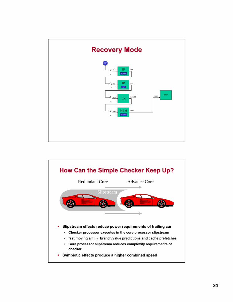
20
Recovery ModeRecovery Mode
result
IF
ID
CT
PC inst
PC
inst
EX
regs
regs
MEM
res/addr
addr result
D-cache
I-cache
RF
How Can the Simple Checker Keep Up? How Can the Simple Checker Keep Up?
Slipstream
Redundant Core Advance Core
Slipstream effects reduce power requirements of trailing carSlipstream effects reduce power requirements of trailing car•• Checker processor executes in the core processor slipstreamChecker processor executes in the core processor slipstream
•• fast moving air fast moving air ⇒⇒ branch/value predictions and cache prefetchesbranch/value predictions and cache prefetches•• Core processor slipstream reduces complexity requirements of Core processor slipstream reduces complexity requirements of
checkerchecker
Symbiotic effects produce a higher combined speedSymbiotic effects produce a higher combined speed

21
How Can the Simple Checker Keep Up? How Can the Simple Checker Keep Up?
Slipstream
Simple Checker Complex Core
Slipstream effects reduce power requirements of trailing carSlipstream effects reduce power requirements of trailing car•• Checker processor executes in the core processor slipstreamChecker processor executes in the core processor slipstream
•• fast moving air fast moving air ⇒⇒ branch/value predictions and cache prefetchesbranch/value predictions and cache prefetches•• Core processor slipstream reduces complexity requirements of Core processor slipstream reduces complexity requirements of
checkerchecker
Symbiotic effects produce a higher combined speedSymbiotic effects produce a higher combined speed
Checker Performance ImpactsChecker Performance ImpactsChecker Checker throughputthroughput bounds core IPCbounds core IPC•• Only cache misses stall checker pipelineOnly cache misses stall checker pipeline•• Core warms cache, leaving few stallsCore warms cache, leaving few stalls
Checker Checker latencylatency stalls retirementstalls retirement•• Stalls decode when speculative stateStalls decode when speculative state
buffers fill (LSQ, ROB)buffers fill (LSQ, ROB)•• Stalled instructions mostly nuked!Stalled instructions mostly nuked!
Storage hazardsStorage hazards stall core progressstall core progress•• Checker may stall core if it lacks resourcesChecker may stall core if it lacks resources
FaultsFaults flush core to recover stateflush core to recover state•• Small impact if faults are infrequentSmall impact if faults are infrequent
0.970.980.991.001.011.021.031.041.05
Relat
ive C
PI
Uber-Check
er
Pico-Check
er
12-cyc
le Check
er
1/4 Cach
e Size
1k Faults

22
Transient Fault Detection Transient Fault Detection via Simultaneous Multithreadingvia Simultaneous Multithreading
Steven K. ReinhardtUniversity of Michigan EECS
Shubhendu S. MukherjeeCompaq Computer Corporation
Rest of System
Sphere of Replication
InputReplication
OutputComparison
Thread 1 Thread 2
Logical boundary of redundant execution within a system• Trade-off between information, time, & space redundancy
Compare & validate output before sending it outside the SoR
Simultaneous Redundant Simultaneous Redundant MultithreadhingMultithreadhing

23
Simultaneous & Redundantly Threaded Simultaneous & Redundantly Threaded Processor (SRT)Processor (SRT)
Sphere of replicationSphere of replication•• Output comparison of committed store instructionsOutput comparison of committed store instructions•• Input replication via load value queueInput replication via load value queue
+ Less hardware+ Less hardware compared to replicated microprocessorscompared to replicated microprocessorsSMT needs ~5% more hardware over SMT needs ~5% more hardware over uniprocessoruniprocessorSRT adds very little hardware overhead to existing SMTSRT adds very little hardware overhead to existing SMT
+ Better performance than complete replication+ Better performance than complete replicationbetter use of resourcesbetter use of resources
+ Lower cost+ Lower costavoids complete replicationavoids complete replicationmarket volume of SMT & SRTmarket volume of SMT & SRT
SRT = SMT + Fault Detection
Fault Tolerant Multiprocessor Fault Tolerant Multiprocessor PlatformsPlatforms
SafetyNetSafetyNetReViveReVive
EndEnd--toto--end invariant checkingend invariant checking

24
Outside of ProcessorOutside of ProcessorHardware faults in shared memory multiprocessorsHardware faults in shared memory multiprocessors•• Mostly transient, some permanent, not Mostly transient, some permanent, not chipkillchipkill•• Interconnection networkInterconnection network
Example: dead switchExample: dead switch
•• Cache coherence protocolsCache coherence protocolsExample: lost coherence messageExample: lost coherence message
Cost vs. Performance vs. AvailabilityCost vs. Performance vs. Availability•• Low CostLow Cost
Simple changes to a few key componentsSimple changes to a few key components
•• Low Performance OverheadLow Performance OverheadHandle frequent operations in hardwareHandle frequent operations in hardware
•• High AvailabilityHigh AvailabilityFast recovery from a wide class of errorsFast recovery from a wide class of errors
Server System Hardware Design SpaceServer System Hardware Design Space
Existing systems get only 2 out of 3 features
Backward Error Recovery
(Tandem NonStop)
Forward Error Recovery
(IBM mainframes)
Servers and PCs
HighAvailability
HighPerformance
LowCost

25
SafetyNetSafetyNet: : Improving the Availability ofImproving the Availability of
Shared Memory Multiprocessors with Shared Memory Multiprocessors with Global Checkpoint/RecoveryGlobal Checkpoint/Recovery
Daniel J. Daniel J. SorinSorin, Milo M. K. Martin,, Milo M. K. Martin,Mark D. Hill, and David A. WoodMark D. Hill, and David A. Wood
Computer Sciences DepartmentComputer Sciences DepartmentUniversity of WisconsinUniversity of Wisconsin——MadisonMadison
SafetyNet AbstractionSafetyNet Abstraction
Processor
Processor
CurrentMemory
Checkpoint
CurrentMemory
checkpointCurrentMemoryVersion
Active(Architectural)
State ofSystem
Most Recently Validated Checkpoint
Recovery Point
Checkpoints Awaiting Validation

26
SafetyNetSafetyNet Checkpoint/RecoveryCheckpoint/RecoverySafetyNetSafetyNet:: allall--hardware scheme [ISCA 2002]hardware scheme [ISCA 2002]•• Periodically take logical checkpoint of multiprocessorPeriodically take logical checkpoint of multiprocessor
MP State: processor registers, caches, memoryMP State: processor registers, caches, memory•• Incrementally log changes to caches and memoryIncrementally log changes to caches and memory•• Consistent Consistent checkpointingcheckpointing performed in performed in logical timelogical time
E.g., every 3000 broadcast cache coherence requestsE.g., every 3000 broadcast cache coherence requests•• Can tolerate >100,000 cycles of error detection latencyCan tolerate >100,000 cycles of error detection latency
time
Active
execution
CP 4CP 3CP 2CP 1Validated
execution
Pending validation –
Still detecting errors
Contribution of Contribution of SafetyNetSafetyNet
SafetyNet: global, consistent checkpointingSafetyNet: global, consistent checkpointing•• Low cost and high performanceLow cost and high performance•• Efficient logical time checkpoint coordinationEfficient logical time checkpoint coordination•• Optimized checkpointing of stateOptimized checkpointing of state•• Pipelined, inPipelined, in--background checkpoint validation background checkpoint validation
Improved availabilityImproved availability•• Avoid crash in case of faultAvoid crash in case of fault•• Same faultSame fault--free performancefree performance
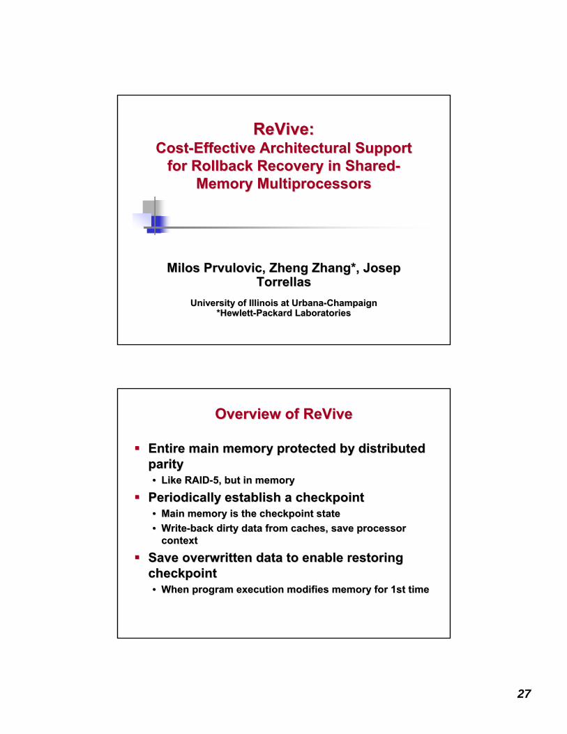
27
ReViveReVive::CostCost--Effective Architectural Support Effective Architectural Support
for Rollback Recovery in Sharedfor Rollback Recovery in Shared--Memory MultiprocessorsMemory Multiprocessors
MilosMilos PrvulovicPrvulovic, , ZhengZheng Zhang*, Josep Zhang*, Josep TorrellasTorrellas
University of Illinois at UrbanaUniversity of Illinois at Urbana--ChampaignChampaign*Hewlett*Hewlett--Packard LaboratoriesPackard Laboratories
Overview of Overview of ReViveReVive
Entire main memory protected by Entire main memory protected by distributed distributed parityparity•• Like RAIDLike RAID--5, but in memory5, but in memory
Periodically establish a checkpointPeriodically establish a checkpoint•• Main memory is the checkpoint stateMain memory is the checkpoint state•• WriteWrite--back dirty data from caches, save processor back dirty data from caches, save processor
contextcontext
Save overwritten data to enable restoring Save overwritten data to enable restoring checkpointcheckpoint•• When program execution modifies memory for 1st timeWhen program execution modifies memory for 1st time

28
Distributed N+1 ParityDistributed N+1 Parity
Parity Data Data
Node 0 Node 1 Node N
Parity Group
Allocation Granularity: pageAllocation Granularity: pageUpdate Granularity: cache lineUpdate Granularity: cache line
. . .Distributed tominimize
contention
Contribution of ReviveContribution of Revive
Low CostLow Cost•• HW changes only to directory controllersHW changes only to directory controllers•• Memory overhead only 12.5% (with 7+1 parity)Memory overhead only 12.5% (with 7+1 parity)
Low Performance OverheadLow Performance Overhead•• Only 6% performance overhead on averageOnly 6% performance overhead on average
High AvailabilityHigh Availability•• Recovery from: systemRecovery from: system--wide transients, loss of one wide transients, loss of one
nodenode•• Availability better than 99.999% (assuming 1 error/ day)Availability better than 99.999% (assuming 1 error/ day)

29
HighHigh--Level Comparison Between Level Comparison Between ReViveReViveand and SafetyNetSafetyNet
No more than 0.4 No more than 0.4 millisecondsmilliseconds
At least 100 At least 100 millisecondsmilliseconds
Output commit latencyOutput commit latency
No lossNo loss66--10% loss10% lossFaultFault--free performancefree performance
NoneNoneMinorMinorSoftware modificationSoftware modification
YesYesNoNoProcessor modificationProcessor modification
Transient & some Transient & some permanentpermanent
Transient & Transient & permanentpermanent
Fault modelFault model
YesYesYesYesBackward error recovery Backward error recovery schemescheme
SafetyNetSafetyNetReViveReVive
Dynamic Verification of Dynamic Verification of EndEnd--toto--End Multiprocessor End Multiprocessor
InvariantsInvariants
Daniel J. SorinDaniel J. Sorin11,, Mark D. HillMark D. Hill22, David A. Wood, David A. Wood2211Department of Electrical & Computer EngineeringDepartment of Electrical & Computer Engineering
Duke UniversityDuke University22Computer Sciences DepartmentComputer Sciences DepartmentUniversity of WisconsinUniversity of Wisconsin--MadisonMadison

30
OverviewOverviewGoal: improve multiprocessor Goal: improve multiprocessor availabilityavailabilityRecent work developed efficient checkpoint/recoveryRecent work developed efficient checkpoint/recovery•• But we can only recover from hardware errors we detectBut we can only recover from hardware errors we detect•• Many hardware errors are hard to detectMany hardware errors are hard to detect
Proposal: Proposal: Dynamic verificationDynamic verification of invariantsof invariants•• Online checking of endOnline checking of end--toto--end system invariantsend system invariants•• Checking performed with Checking performed with distributed signature analysisdistributed signature analysis•• Triggers recovery if invariant is violatedTriggers recovery if invariant is violated
ResultsResults•• Detects previously undetectable hardware errorsDetects previously undetectable hardware errors•• Negligible performance overhead for errorNegligible performance overhead for error--free executionfree execution
Why Local Information IsnWhy Local Information Isn’’t Sufficientt Sufficient
P1 P4P3P2
switch
switch
switch
Owned
Broadcast Request for Exclusive
InvalidData Response
fault!
Neither P1 nor P2 can detect that an error has occurred!
SharedModified

31
Distributed Signature AnalysisDistributed Signature AnalysisReduces long history of events into Reduces long history of events into small small signaturesignature•• Signatures map Signatures map almostalmost--uniquely to event historiesuniquely to event histories
P1 Signature P2 Signature
Event N at P1
:
Event 2 at P1
Event 1 at P1
Event N at P2
:
Event 2 at P2
Event 1 at P2
Checker
P2’s signatureP1’s signature
} Check periodically in logical time(every 3000 requests)
Commercial ProcessorsCommercial Processors

32
Different Abstraction of ReplicationDifferent Abstraction of Replication
Rest of System
OutputComparison
InputReplication
microprocessor microprocessor
Replicated lockstepped mirror processors
Rest of System
OutputComparison
InputReplication
Pipeline 1
Replicated pipelines in same die
Pipeline 2
S/390 G5 CPU Fault Tolerant ApproachS/390 G5 CPU Fault Tolerant Approach
Dual modular redundancy within Dual modular redundancy within microprocessormicroprocessor•• Replicate and Replicate and locksteppedlockstepped pipelines (I and Epipelines (I and E--unit) unit)
Parity for cache data and data pathsParity for cache data and data pathsError checking of control and ALUError checking of control and ALUDynamic CPU RecoveryDynamic CPU Recovery•• RR--unit unit
ECCECC--protected Register File; Checkpoint Arrayprotected Register File; Checkpoint ArrayProviding Backward Error Recovery (BER) by comparing results froProviding Backward Error Recovery (BER) by comparing results from m replicated, replicated, locksteppedlockstepped pipelinespipelines
Dynamic CPU SparingDynamic CPU Sparing•• Scan machine state information from failed CPU into spare CPUScan machine state information from failed CPU into spare CPU•• System to be restored to full capacity in less than one secondSystem to be restored to full capacity in less than one second

33
S/390 G5 Memory System S/390 G5 Memory System Fault Tolerant ApproachFault Tolerant Approach
L1 $L1 $•• writewrite--through through •• Byte parityByte parity•• Recover transient L1 failure by instruction retryRecover transient L1 failure by instruction retry•• Recover permanent failure by deleting cacheRecover permanent failure by deleting cache--lineline
L2 $L2 $•• Each L2 cache is shared by 6 microprocessorsEach L2 cache is shared by 6 microprocessors•• Protected by SEC/DED ECC Protected by SEC/DED ECC •• Avoiding error from permanent fault by using cacheAvoiding error from permanent fault by using cache--delete delete
capabilitycapabilityMain memory Main memory •• Using SEC/DED ECCUsing SEC/DED ECC•• Automatic onAutomatic on--line repair by using builtline repair by using built--in spare chipsin spare chips
S/390 G5 I / O and Power S/390 G5 I / O and Power Fault Tolerant ApproachFault Tolerant Approach
I/O Subsystem designed I/O Subsystem designed •• Redundant paths between all devices and main memoryRedundant paths between all devices and main memory•• Parallel Parallel SysplexSysplex Provides ServerProvides Server--toto--server Connectionserver Connection
99.999%99.999% availability with two or more interconnected mainframeavailability with two or more interconnected mainframe
Power supply Power supply •• Fully RedundancyFully Redundancy
BatteryBatteryACAC--toto--DC ConvertersDC ConvertersDCDC--toto--DC convertersDC convertersFan/Compressor assembliesFan/Compressor assemblies

34
Fault Detection in Compaq Himalaya SystemFault Detection in Compaq Himalaya System
R1 ← (R2)
InputReplication
OutputComparison
Memory covered by ECCRAID array covered by parityServernet covered by CRC
R1 ← (R2)
microprocessor microprocessor
Replicated Microprocessors + Cycle-by-Cycle Lockstepping
Tandem HP Tandem HP NonStopNonStop ServersServersLoosely coupled massively parallel computerLoosely coupled massively parallel computerTwo replicated, lockTwo replicated, lock--stepped MIPS R4400 stepped MIPS R4400 RISC processors (mirroring) in each logical RISC processors (mirroring) in each logical processor compare execution by externalprocessor compare execution by external--chip comparisonchip comparisonL2 Cache, main memory, and operating L2 Cache, main memory, and operating system are all independentsystem are all independentControlled by operating systemControlled by operating system100% Design overhead100% Design overhead

35
ReferencesReferences1.1. C. Constantinescu C. Constantinescu ‘‘Trend and Challenge in VLSI Circuit ReliabilityTrend and Challenge in VLSI Circuit Reliability’’ intelintel2.2. H. T. Nguyen H. T. Nguyen ‘‘A Systematic Approach to Processor SER Estimation and SolutionsA Systematic Approach to Processor SER Estimation and Solutions’’3.3. P. P. ShivakumarShivakumar et. al, et. al, ‘‘Modeling the effect of Technology trends on Soft Error Rate of CModeling the effect of Technology trends on Soft Error Rate of Combinational ombinational
LogicLogic’’4.4. P. P. ShivakumarShivakumar ‘‘FaultFault--TolernatTolernat Computing for Radiation EnvironmentComputing for Radiation Environment’’ Ph.D. Thesis Stanford UniversityPh.D. Thesis Stanford University5.5. M. M. NicolaidisNicolaidis ‘‘Time Redundancy Based SoftTime Redundancy Based Soft--Error Tolerance to Rescue Nanometer TechnologiesError Tolerance to Rescue Nanometer Technologies’’6.6. L. L. AnghelAnghel, et. al., et. al. ‘‘Cost Reduction and Evaluation of a Temporary Faults Detecting TeCost Reduction and Evaluation of a Temporary Faults Detecting Techniquechnique’’7.7. L. L. anghelanghel, et. al. , et. al. ‘‘Evaluation of Soft Error Tolerance Technique based on Time and/oEvaluation of Soft Error Tolerance Technique based on Time and/or Space Redundancyr Space Redundancy’’
ICSDICSD8.8. I. Koren, University of I. Koren, University of MassachsuttsMassachsutts ECE 655 Lecture Notes 4ECE 655 Lecture Notes 4--5 5 ‘‘CodingCoding’’9.9. ITRS 2003 Report ITRS 2003 Report 10.10. J. von Neumann, "Probabilistic logic and the synthesis of reliabJ. von Neumann, "Probabilistic logic and the synthesis of reliable organisms from unreliable le organisms from unreliable
components," components," 11.11. R. E. Lyons, et. al. R. E. Lyons, et. al. ‘‘The Use of TripleThe Use of Triple--Modular Redundancy to Improve Computer ReliabilityModular Redundancy to Improve Computer Reliability’’12.12. D. G. Mavis, et. al. D. G. Mavis, et. al. ‘‘Soft Error Rate Mitigation Techniques for Modern Microcircuits.Soft Error Rate Mitigation Techniques for Modern Microcircuits.’’ IEEE 40th Annual IEEE 40th Annual
International Reliability Physics Symposium 2002.International Reliability Physics Symposium 2002.13.13. C. Weaver, et. al. C. Weaver, et. al. ‘‘A Fault Tolerant Approach to Microprocessor DesignA Fault Tolerant Approach to Microprocessor Design’’ DSNDSN’’010114.14. J. Ray, et. al. J. Ray, et. al. ‘‘Dual Use of Superscalar Datapath for TransientDual Use of Superscalar Datapath for Transient--Fault Detection and RecoveryFault Detection and Recovery’’, Proceedings , Proceedings
of the 34th Annual Symposium on Microarchitecture (MICROof the 34th Annual Symposium on Microarchitecture (MICRO’’01). 01). 15.15. J. B. Nickel, et. al. J. B. Nickel, et. al. ‘‘REESE: A Method of Soft Error Detection in MicroprocessorsREESE: A Method of Soft Error Detection in Microprocessors’’, Proceedings of the , Proceedings of the
International Conference on Dependable Systems and Networks (DSNInternational Conference on Dependable Systems and Networks (DSN’’01).01).16.16. S. Reinhardt, et. al. S. Reinhardt, et. al. ‘‘Transient Fault Detection Simultaneous MultithreadingTransient Fault Detection Simultaneous Multithreading’’
ReferencesReferences1.1. D. D. SiewiorekSiewiorek ‘‘Fault Tolerance in Commercial ComputersFault Tolerance in Commercial Computers’’ CMUCMU2.2. W. Bartlett, et. al. W. Bartlett, et. al. ‘‘Commercial Fault Tolerance: A Tale of Two SystemsCommercial Fault Tolerance: A Tale of Two Systems’’ IEEE Dependable and Secure IEEE Dependable and Secure
Computing 2004 Computing 2004 3.3. T. T. SlegelSlegel et.alet.al ‘‘IBMIBM’’s S/390 G5 Microprocessor Designs S/390 G5 Microprocessor Design’’4.4. L. L. SpainhowerSpainhower, , et.alet.al, , ‘‘IBM S/390 Parallel Enterprise Server G5 fault tolerance: A histoIBM S/390 Parallel Enterprise Server G5 fault tolerance: A historical approachrical approach’’5.5. D. D. BossenBossen et.alet.al ‘‘Fault tolerant design of the IBM Fault tolerant design of the IBM pSeriespSeries 690 system using POWER4 processor 690 system using POWER4 processor
technologytechnology’’6.6. ‘‘Tandem HP HimalayaTandem HP Himalaya’’ White PaperWhite Paper7.7. Fujitsu SPARC64 V Microprocessor Provides Foundation for PRIMEPOFujitsu SPARC64 V Microprocessor Provides Foundation for PRIMEPOWER Performance and Reliability WER Performance and Reliability
LeadershipLeadership8.8. D. J. D. J. SorinSorin, et. al. , et. al. ‘‘SafetyNetSafetyNet: Improving the Availability of : Improving the Availability of SharedMemorySharedMemory Multiprocessors with Global Multiprocessors with Global
Checkpoint/Recovery.Checkpoint/Recovery.’’9.9. MilosMilos PrvulovicPrvulovic, et. al. , et. al. ‘‘ReVive:CostReVive:Cost--Effective Architectural Support for Rollback Recovery in SharedEffective Architectural Support for Rollback Recovery in Shared--
Memory MultiprocessorsMemory Multiprocessors’’10.10. J. J. SmolensSmolens, , et.alet.al ‘‘Fingerprinting: Bounding Fingerprinting: Bounding SoftErrorSoftError Detection Latency and BandwidthDetection Latency and Bandwidth’’11.11. D. D. SorinSorin, , et,alet,al ‘‘Dynamic Verification of EndDynamic Verification of End--toto--End Multiprocessor InvariantsEnd Multiprocessor Invariants’’

36
BackupBackup
Processor Core Fault ToleranceProcessor Core Fault ToleranceAdding redundancy into pipeline stagesAdding redundancy into pipeline stagesObservationObservation•• Modern microprocessor has support to recovery from exception / Modern microprocessor has support to recovery from exception /
misprediction, before commit stagemisprediction, before commit stage•• Detect / recover from error by checking each instruction before Detect / recover from error by checking each instruction before inin--order order
commitmentcommitment
Instruction reInstruction re--execution (REESE, Dual Use)execution (REESE, Dual Use)•• ObservationObservation
Aggressive Aggressive OoOOoO. processor will not 100% utilize system resources. processor will not 100% utilize system resources# of Committed instructions much less than # of fetched instruct# of Committed instructions much less than # of fetched instruction on averageion on average
Checker pipeline (DIVA)Checker pipeline (DIVA)•• Passing instruction to checker pipeline before commit stagePassing instruction to checker pipeline before commit stage•• Complexity of checker pipeline is much less than that of main prComplexity of checker pipeline is much less than that of main processorocessor
Checker only deals with inChecker only deals with in--order retirement queue of the instruction from main order retirement queue of the instruction from main pipelinepipelineNo need to deal with speculative instructions No need to deal with speculative instructions

37
Circuit Techniques: Circuit Techniques: (1) SEU Immune Latch(1) SEU Immune Latch
The two extra inverters together with the normal gating transistThe two extra inverters together with the normal gating transistors ors provide three independent delay stages for absorbing glitchesprovide three independent delay stages for absorbing glitchesGlitches are absorbed whether generated internally, or whether cGlitches are absorbed whether generated internally, or whether coming oming in on the Data or clock (GB) lines, as long as the timing guidelin on the Data or clock (GB) lines, as long as the timing guidelines are ines are followed. What is shown is a latch, which is 1/2 of the common Dfollowed. What is shown is a latch, which is 1/2 of the common D--flipflip--flop circuit. flop circuit.
Related Work: Related Work: SafetyNetSafetyNetTypes of recoverable errorsTypes of recoverable errors•• ReViveReVive: Permanent (loss of a node)+Transient: Permanent (loss of a node)+Transient•• SafetyNetSafetyNet: Transient; perm only w/ redundant devices: Transient; perm only w/ redundant devices
HW modificationsHW modifications•• ReViveReVive: Directory controller only: Directory controller only•• SafetyNetSafetyNet: Memory, caches, coherence protocol: Memory, caches, coherence protocol
Performance OverheadPerformance Overhead•• 6% with 6% with ReViveReVive, negligible with , negligible with SafetyNetSafetyNet

38
Implementing Distributed Signature AnalysisImplementing Distributed Signature Analysis
All components cooperate to perform All components cooperate to perform checkingchecking•• Component = cache controller or memory Component = cache controller or memory
controllercontrollerEach component contains:Each component contains:•• Local signature registerLocal signature register•• Logic to compute signature updatesLogic to compute signature updates
System contains:System contains:•• System controller that performs check functionSystem controller that performs check function
Use distributed signature analysis for dynamic Use distributed signature analysis for dynamic verificationverification•• Verify endVerify end--toto--end invariantsend invariants
Two invariant checkersTwo invariant checkersMessage invariantMessage invariant•• all nodes see all nodes see same total ordersame total order of broadcast cache coherence of broadcast cache coherence
requestsrequests•• Update: for each incoming broadcast, Update: for each incoming broadcast, ““addadd”” AddressAddress•• Check: error if all signatures arenCheck: error if all signatures aren’’t equal t equal
Cache coherence invariantCache coherence invariant•• All coherence upgrades cause downgradesAll coherence upgrades cause downgrades
Upgrade: increase permissions to block Upgrade: increase permissions to block (e.g., (e.g., nonenone readread))Downgrade: decrease permissions (e.g., write Downgrade: decrease permissions (e.g., write read)read)
•• Update: add Address for upgradeUpdate: add Address for upgradesubtract Address for downgradesubtract Address for downgrade
•• Check: error if sum of all signatures doesnCheck: error if sum of all signatures doesn’’t equal 0t equal 0

39
Distributed Parity Update in HWDistributed Parity Update in HW
Dir
Mem
WB Line X
Wr
Dir
Mem
Dir
Mem
Rd
Par
Rd Wr
Par Ack
XORXOR
Home of Line X Home ofparity for Line X