low power single chip radio technologies for …
TRANSCRIPT

1
LOW POWER SINGLE CHIP RADIO TECHNOLOGIES FOR WIRELESS SENSOR NETWORK APPLICATIONS
By
WUTTICHAI LERDSITSOMBOON
A DISSERTATION PRESENTED TO THE GRADUATE SCHOOL OF THE UNIVERSITY OF FLORIDA IN PARTIAL FULFILLMENT
OF THE REQUIREMENTS FOR THE DEGREE OF DOCTOR OF PHILOSOPHY
UNIVERSITY OF FLORIDA
2011

2
© 2011 Wuttichai Lerdsitsomboon

3
To my parents and my sisters

4
ACKNOWLEDGMENTS
I would like to express my deep gratitude and appreciation to my advisor,
Professor Kenneth K. O, for his guidance, inspiration, encouragement, patience and
constant support during my Ph.D program. He gave me a great opportunity to be part of
the SiMICs group where I have gained much valuable experiences. What I have learned
while in this group is priceless and will benefit me for the rest of my life. I would like to
thank Professor Jenshan Lin, Professor Rizwan Barshirullah and Professor Oscar D.
Crisalle for their interest in my research work and their time commitment in serving on
my committee.
I would like to thank my colleagues Hsinta Wu, Tie Sun, Ruonan Han, Ning Zhang,
Chuying Mao, Swaminathan Sankaran, Seon-Ho Hwang, Dr. Choongyul Cha, Dongha
Shim, Kyujin Oh and Minsoon Hwang for their endless friendship, discussions and
suggestions which have significantly contributed to this work. I am also grateful for the
advice from other group members, Yanping Ding, Changhua Cao, Yu Su, Chikuang Yu,
Jau-Jr Lin, Haifeng Xu, Kwangchun Jung, Myoung Hwang, Zhe Wang, Teyu Kao,
Chakravartula Shashank Nallani, Gayathri Devi Sridharan, Chiehlin Wu, Yanghun Yun
and Gyungseon Seol. I have been fortunate to work with these great people.
My deepest appreciation goes to my girl-friend, Pajaree Fah Thongpravati. I
greatly respect for her love, patience, support and never giving up. She has always
believed in me during bad and good times throughout the years.
Finally, I am very grateful to my parents and my sisters for their endless support,
unconditional love and encouragement throughout the years. My parents always
support me and are always there when I need help. I dedicate this work to my mother
and father.

5
TABLE OF CONTENTS page
ACKNOWLEDGMENTS .................................................................................................. 4
LIST OF TABLES ............................................................................................................ 7
LIST OF FIGURES .......................................................................................................... 8
ABSTRACT ................................................................................................................... 13
CHAPTER
1 INTRODUCTION .................................................................................................... 15
Motivation ............................................................................................................... 15 Research Goals ...................................................................................................... 17 Organization of the Dissertation .............................................................................. 19
2 2.4-GHz µNODE SYSTEM ..................................................................................... 21
Wireless Receiver Basics ....................................................................................... 21 Sensitivity ......................................................................................................... 21 Selectivity ......................................................................................................... 23 Dynamic Range ................................................................................................ 25
Receiver Architecture Overview .............................................................................. 26 Heterodyne Receiver ........................................................................................ 26 Homodyne Receiver ......................................................................................... 27
2.4-GHz µNode System Overview .......................................................................... 28 Summary ................................................................................................................ 31
3 ANTENNA CHARACTERISTICS ............................................................................ 33
Monopole Antenna Overview .................................................................................. 34 Off-Chip Monopole Antenna Investigation .............................................................. 35 On-Chip Monopole Antennas .................................................................................. 38
On-Chip Monopole Test Structures .................................................................. 38 On-Chip Monopole Input Impedance ................................................................ 41 Antenna Pair Gain, Ga, for On-Chip Monopoles ............................................... 45 On-Chip Antenna Close to Ground ................................................................... 53 On-Chip Antenna Radiation Pattern ................................................................. 55 Effect of Surrounding Objects on Antenna Performance .................................. 56 On-Chip Antenna for µNode Operating at 2.4 GHz .......................................... 63
Summary ................................................................................................................ 64

6
4 THE WIRELESS SWITCH DESIGN FOR µNODE SYSTEM .................................. 65
Wireless Switch Operating Range .......................................................................... 65 Wireless Switch Architecture .................................................................................. 67 Operation Modes .................................................................................................... 70 Circuit Designs ........................................................................................................ 71
Mechanism of Voltage Multiplier ....................................................................... 71 Radio Frequency-to-Direct Current Component (RF-to-DC) Converter ............ 74 Envelope Detector, Limiter & RF Clamp and Power-on-Reset Circuit. ............. 80 Transmit/Receive (T/R) Switch for µNode Transceiver .................................... 82
Experimental Results .............................................................................................. 84 Summary ................................................................................................................ 92
5 LOW POWER RECEIVER FRONT-END DESIGN ................................................. 93
Receiver Front-End Architecture ............................................................................. 93 Circuit Designs ........................................................................................................ 94
Ring-Oscillator Based Phase Locked Loop (PLL) ............................................ 94 Impedance Transformation Network ................................................................ 96 Passive Mixers ............................................................................................... 101 Baseband Amplifier ........................................................................................ 107 25% Local Oscillator (LO) Driver .................................................................... 108 µNode Receiver Front-End ............................................................................. 109
Experimental Results ............................................................................................ 112 Summary .............................................................................................................. 119
6 SUMMARY AND SUGGEST FUTURE WORK ..................................................... 120
Research Summary .............................................................................................. 120 Suggested Future Work ........................................................................................ 121
Improve the Performance of On-Chip Antennas. ............................................ 121 Improve the Performance of the Wireless Switch. .......................................... 121 Improve the Performance of the Receiver Front-End. .................................... 121 Complete the Receiver Chain. ........................................................................ 122
APPENDIX: PRINTED CIRCUIT BOARD DESIGN.................................................... 123
LIST OF REFERENCES ............................................................................................. 127
BIOGRAPHICAL SKETCH .......................................................................................... 134

7
LIST OF TABLES
Table page 2-1 Link analysis summary for 2.4-GHz µNode systems .......................................... 31
3-1 Simulation results for antenna gain (-x direction) at 2.4 GHz.............................. 58
5-1 Performance comparison.................................................................................. 119

8
LIST OF FIGURES
Figure page 1-1 Conceptual diagrams of µNode systems. ........................................................... 15
1-2 Wireless sensor network applications. ................................................................ 16
1-3 µNode device size. ............................................................................................. 16
1-4 Simplified radio architecture of µNode system. .................................................. 18
1-5 Off-chip and on-chip antennas............................................................................ 18
1-6 Conceptual diagram of non-contact switch. ........................................................ 19
2-1 Heterodyne receiver architecture. ....................................................................... 26
2-2 Homodyne receiver architecture. ........................................................................ 27
2-3 Simplified µNode transceiver block diagram. ...................................................... 29
3-1 Helix-based chip antenna. .................................................................................. 36
3-2 Ceramic chip antenna (AN3216) and recommended printed circuit board (PCB) design. ..................................................................................................... 36
3-3 Chip antennas on PCB’s with varying sizes and measured return loss, |S11|. .... 37
3-4 Antenna pair gain (Ga) measurement setup and result. ...................................... 38
3-6 On-chip monopole test structures. ...................................................................... 40
3-7 Fabricated antenna test structures. .................................................................... 40
3-8 |S11| measurement setup for on-chip antennas. ................................................. 41
3-9 Measured |S11| of linear on-chip monopoles. ...................................................... 42
3-10 Measured |S11| of zigzag on-chip monopoles. .................................................... 42
3-11 Measured real(Zin) of linear monopole antennas. ............................................... 43
3-12 Measured real(Zin) of zigzag monopole antennas............................................... 43
3-13 Measured imaginary(Zin) of linear monopole antennas....................................... 44
3-14 Measured imaginary(Zin) of zigzag monopole antennas. .................................... 44

9
3-15 Ga measurement setup for on-chip antennas. .................................................... 45
3-16 Measured antenna pair gain (Ga) at 5.8 GHz vs. distance.................................. 46
3-17 Measured antenna pair gain (Ga) vs. distance for linear-type antennas. ............ 48
3-18 Measured antenna pair gain (Ga) vs. distance for zigzag-type antennas............ 49
3-19 Estimated gain for on-chip antennas. ................................................................. 50
3-20 Cascade MPH-F4 Probe holder. ......................................................................... 51
3-21 Simulated structures for on-chip antennas. ........................................................ 51
3-22 Simulation results for antenna gain vs. frequencies. .......................................... 52
3-23 Ga measurement setup for antennas placed 5 mm from ground. ....................... 53
3-24 Measured antenna pair gain (Ga) at 5.8 GHz vs. distance for antennas Z1 and Z5. ............................................................................................................... 54
3-25 Measured antenna pair gain (Ga) at 5.2 GHz vs. distance for antennas Z1 and Z5. ............................................................................................................... 54
3-26 Measured antenna pair gain Ga at 2.4 GHz vs. distance for antennas Z1 and Z5. ...................................................................................................................... 55
3-27 Measured radiation patterns of structure Z1 and Z5 at 5.8 and 2.4 GHz. ........... 56
3-28 Simulation structures for antennas close to other objects................................... 57
3-29 Simulated antenna |S11|. ..................................................................................... 57
3-30 Test structures for different types of antennas and surrounding objects. ........... 59
3-31 Measured |S11| for off-chip antennas. ................................................................. 59
3-32. Measured |S11| for PCB antennas. ...................................................................... 60
3-33 Measured |S11| for on-chip antennas mounted on glass slides. .......................... 60
3-34 Measured |S11| for on-chip antennas mounted on PCB’s. .................................. 61
3-35 Measured Ga for off-chip antennas with surrounding objects at 2.4 GHz. .......... 62
3-36 Measured Ga for on-chip antennas with surrounding objects at 2.4 GHz. .......... 62
3-37 On-chip antenna for µNode, and simulated |S11|. ............................................... 63

10
3-38 Simulated antenna gain. ..................................................................................... 64
4-1 Operating range estimation for wireless switch. ................................................. 65
4-2 Architecture of µNode system. ........................................................................... 68
4-3 Simplified schematic for wireless switch in µNode system. ................................ 69
4-4 Operation Modes: (top) Power-up (PUx) Mode, (bottom) Transceiver (TRx) Mode. ................................................................................................................. 71
4-5 Voltage multiplier or voltage doubler circuit. ....................................................... 72
4-6 Mechanism of voltage multiplier circuit. .............................................................. 74
4-7 The radio frequency-to-direct current component (RF-to-DC) converter with a matching network. .............................................................................................. 75
4-8 N-type Schottky barrier diode layout and its cross section. ................................ 78
4-9 Diode equivalent model with associated parasitics. ............................................ 78
4-10 Current-voltage characteristics of measured Schottky Barrier Diodes. ............... 79
4-11 Simulated power conversion efficiency for a 5-stage RF-to-DC converter. ........ 80
4-12 Sub-circuits for Wireless Switch. ........................................................................ 81
4-13 Input impedance of the entire system for both operating modes: Power-up (PUx) and Transceiver (TRx) modes. ................................................................. 83
4-14 Chip die micrograph. .......................................................................................... 84
4-15 Small-signal |S11| of the RF-to-DC converter with a matching network. .............. 85
4-16 Large-signal |S11| of the RF-to-DC converter with matching network at 5.7 GHz. ................................................................................................................... 86
4-17 DC output voltage vs. available power, PAvail. ..................................................... 87
4-18 Power conversion efficiency vs. available power, PAvail. ..................................... 87
4-19 Measured performance of T/R switch. ................................................................ 89
4-20 Measured performance of T/R switch integrated with a wireless switch in Power-up (PUx) mode. ....................................................................................... 90
4-21 Measured performance of T/R switch integrated with a wireless switch in Transceiver (TRx) mode. .................................................................................... 91

11
4-22 Measured 1-dB compression points of T/R switches with and without a wireless switch. ................................................................................................... 91
5-1 Receiver front-end architecture. ......................................................................... 93
5-2 Charge pump based type-II phase locked loop (PLL) for generating local oscillator (LO) signal. .......................................................................................... 95
5-3 4-Stage ring oscillator. ........................................................................................ 95
5-4 Tapped capacitor resonator as an impedance transformation network. ............. 96
5-5 Transformation of tapped capacitor resonator. ................................................... 98
5-6 Resonant frequency, fo, of tapped capacitor resonator vs. variation of C2. ......... 98
5-7 Simulated performance of matching network with varying QL: noise figure and voltage gain. .............................................................................................. 100
5-8 Simulated performance of matching network with various QL: |S11| and |S22|,. . 100
5-9 Schematic and equivalent models for a single-balanced passive mixer. .......... 102
5-10 Switching conductance with pulse approximation for mixer conversion gain analysis. ........................................................................................................... 103
5-11 Equivalent model for mixer output impedance calculation. ............................... 104
5-12 Simulated real part of input impedance, Real(Zi), of a single-balanced passive mixer vs. RF input frequency. .............................................................. 105
5-13 Simulated noise figure of a single-balanced passive mixer with various transistor sizes. ................................................................................................. 106
5-14 Baseband amplifier with gain control. ............................................................... 107
5-15 Schematic for 25% duty-cycle LO driver. .......................................................... 108
5-16 25% duty-cycle LO wave form. ......................................................................... 109
5-17 Simplfied schematic of µNode receiver front-end. ............................................ 110
5-18 Simulated conversion gain and noise figure of receiver versus the mixer transistor width. ................................................................................................ 111
5-19 Chip die photo and a printed circuit board (PCB). ............................................ 112
5-20 Baseband amplifier test structure and its measured performance. ................... 113

12
5-21 Measurement setup. ......................................................................................... 114
5-22 Measured PLL output. ...................................................................................... 115
5-23 Measured |S11| of the receiver front-end. .......................................................... 115
5-24 Voltage conversion gain of the receiver front-end. ........................................... 116
5-25 Measured noise figure of the receiver front-end. .............................................. 117
5-26 Measured second-order and third-order input intercept points (IIP2 and IIP3). . 118
5-27 Power consumption summary for µNode front-end. ......................................... 118
A-1 Die micrograph of µNode front-end including bond pads. ................................. 123
A-2 Bonding area for µNode PCB. .......................................................................... 124
A-3 PCB layout for both top and bottom layers. ...................................................... 125
A-4 Top overlay layer describing the location of the components on PCB. ............. 126

13
Abstract of Dissertation Presented to the Graduate School of the University of Florida in Partial Fulfillment of the Requirements for the Degree of Doctor of Philosophy
LOW POWER SINGLE CHIP RADIO TECHNOLOGIES FOR WIRELESS SENSOR
NETWORK APPLICATIONS
By
Wuttichai Lerdsitsomboon
August 2011
Chair: Kenneth K.O Major: Electrical and Computer Engineering
µNode is a sensor node using a single chip radio. It can serve as a node to form a
wireless sensor network. This node requires a small form factor, low power and low
cost.
Due to its low cost and easy integration, on-chip antennas in CMOS processes
have been studied over last 15 years. Simulations suggest that a 1-cm on-chip antenna
covered by dielectric material with dielectric constant equal to 4 can form a wireless
communication link at 2.4 GHz with a useful distance of 20 m. On-chip antennas are
also less sensitive to surrounding objects compare to off-chip antennas especially when
a nearby silicon chip is considered. This is important for a small form factor radio such
as µNode.
A technique for integrating a wireless switch to turn an M&MTM sized radio on or off
is demonstrated using a 130-nm digital CMOS process. The switch circuit like a passive
radio frequency identification system picks up an amplitude-modulated 5.8-GHz carrier
and converts it to DC to power up a portion of radio connected to a coin-cell battery.
The radio uses a 2.4/5.8 GHz dual band antenna. This wireless switch is added

14
between the antenna and transmit/receive (T/R) switch of the radio. By incorporating an
impedance transformation network, the wireless switch input sensitivity is reduced to ~-
13 dBm. Inclusion of this circuit degrades the maximum transmitted power and
sensitivity of 2.4-GHz transceiver by ~0.3 - 0.5 dB. An RF clamp of wireless switch also
limits the input power above ~12 dBm to protect the switch and transceiver. The
wireless switch occupies an area of ~0.24 mm2.
Approaches to reduce power consumption and area are incorporated into a 2.4-
GHz receiver front-end incorporating a phase locked loop (PLL). The 2.4-GHz PLL
using a relaxation voltage-controlled oscillator achieves phase noise of -92.8 dBc/Hz at
1-MHz frequency offset. The LO driver and mixer are co-optimized for gain, noise figure
and power consumption. The front-end occupies an active area of 0.12 mm2 and
achieves voltage conversion gain of 40 dB, noise figure of 9.2 dB at 1-MHz intermediate
frequency while consuming only ~3.5 mW.

15
CHAPTER 1 INTRODUCTION
Motivation
With the rapid evolution of wireless communication industry over the last few
decades, research on wireless communication circuits and systems has received a
great deal of attention. This has fueled a strong drive for high performance radio
frequency (RF) integrated circuits (IC’s) in silicon process, especially complementary
metal oxide semiconductor (CMOS) technology, due to its low cost and high level of
integration. Figure 1-1 shows conceptual diagrams of a radio with ultimate integration
called µNode [1]-[12]. It integrates antennas, RF circuits, analog baseband circuits,
digital baseband and control circuits, and an on-chip reference. This CMOS system-on-
chip (SoC) device can serve as a node to form a wireless sensor network. Figure 1-2
shows some examples of wireless sensor network applications.
A version operating at 24 GHz that could be packaged with a battery in a volume
with the size of an M&MTM candy as shown in Figure 1-3 has been proposed [1]-[12].
This high operating frequency resulted in high power consumption that increased the
size of a battery. This in turn limited system size and operation life time.
Figure 1-1. Conceptual diagrams of µNode systems.

16
Figure 1-2. Wireless sensor network applications.
Figure 1-3. µNode device size.
To make the node more power efficient, approaches to lower the operating
frequencies are being investigated. Lowering the frequency from 24 GHz down to 2.4
GHz gives several advantages. For instance, the power consumption of entire system
can be reduced by a factor of ~3 and the communication range can be increased by a

17
factor of ~3-4 due to lower path loss at 2.4 GHz for a given transmitted power level [12].
Longer communication range reduces the node density for a given area which
eventually leads to lower system cost.
Like the vision from the previous research, the package size target of this new
µNode is still that of an M&MTM candy. A major challenge is to reduce the size of an
antenna operating at 2.4 GHz. Since the wavelength is longer at lower operating
frequencies, it is challenging to realize an antenna which can fit inside the µNode
package while still providing useful performance. Furthermore, it is difficult to power up
each node individually by flipping a mechanical switch because of the small form factor.
A subsystem which can rapidly turn on many of nodes simultaneously is thus
necessary.
Research Goals
Simplified radio architecture of µNode system is shown in Figure 1-4. This new
system architecture consists of an antenna, a wireless switch for powering up the
circuit, a transceiver front-end (transmitter and receiver chains), a frequency generator,
a demodulator and a baseband processor. This new system employs only one antenna
to reduce the chip area and, thus, makes the system more compact. The goals for this
new µNode system research are realizing compact antennas, developing a technique of
integrating wireless switch, and lowering the overall power consumption of RF
subsystems.
Due to the small form factor of µNode, a compact antenna that can fit inside the
package while achieving useful performance at 2.4 GHz is important. Investigation of
off-chip and on-chip antenna characteristics at that frequency is thus required. Figure 1-

18
5 shows samples of off-chip and on-chip antennas which will be investigated in this
research.
Figure 1-4. Simplified radio architecture of µNode system.
Figure 1-5. Off-chip and on-chip antennas.
Since a µNode system requires post fabrication calibration [13], [15], ability to turn
the battery power on and off is required. As mentioned before, it is difficult to place a
physical switch into a small package such as µNode. Therefore, the concept of wireless
switch has been proposed to accomplish this function. Figure 1-6 shows a conceptual

19
diagram of a non-contact switch to turn on single chip radios [16]. It consists of an input
matching network, rectifying element, low-pass filter & regulator and a switch & control
circuit. This wireless switch is added at the node between the antenna and the
transceiver front-end. Incorporation of the wireless switch function should utilize as
much of the infrastructure available in the single chip radio while not significantly
degrading the performance of a main radio link.
Figure 1-6. Conceptual diagram of non-contact switch.
Finally, the disposable M&MTM sized sensor node is powered by a coin-cell
battery. Because of this, both the peak and average power consumption of the wireless
transceiver limit the lifetime and applications. Lowering the power consumption of the
transceiver is another critical challenge. For this, a low-power 2.4-GHz receiver front-
end design is studied.
Organization of the Dissertation
Chapter 2 reviews the wireless receiver basics. The overviews of receiver
architectures are presented. Then, 2.4-GHz µNode system is introduced. Chapter 3
discusses the characteristics of two major types of antennas: off-chip and on-chip
antennas. The antenna studies are done through simulations and measurements under
several conditions and in different operating frequencies. The effects of surrounding
objects on antenna performance are also investigated, especially when the small form

20
factor like µNode is considered. Finally, suggestion for an on-chip antenna that can
satisfy µNode requirement is discussed. Chapter 4 discusses the design and
characterization of wireless switch circuit. In this chapter, the general design techniques
of dual band and operation modes for wireless switch as well as key parameters for
wireless switch design are described. Design and optimization of Schottky barrier
diodes (SBD) used in the RF-to-DC converter of wireless switch are also discussed.
Chapter 5 presents the low power CMOS receiver front-end design. The 2.4-GHz
receiver prototype incorporating with a phase-locked loop (PLL) is also presented.
Important design issues and techniques for reducing the power consumption of receiver
front-end are discussed. Finally, Chapter 6 summarizes the overall research.
Conclusions for three major research goals for making µNode concept practical are
given. Then, suggested future works are discussed.

21
CHAPTER 2 2.4-GHZ µNODE SYSTEM
Sensitivity and selectivity are the two fundamental figures of merit for the receiver
and are dependent on various figures of merit of sub-blocks such as noise, linearity and
gain distribution. Also, these two parameters are directly related to the dynamic range of
receiver. This chapter reviews basic parameters which are important for wireless
receiver design and also discusses two major types of receiver architecture: heterodyne
and homodyne receivers. Following this, the system for 2.4-GHz µNode is presented.
Wireless Receiver Basics
Sensitivity
Sensitivity is defined as the minimum signal power level at the receiver input that
leads to receiver output with sufficient signal-to-noise ratio (SNR). The overall sensitivity
is related to the noise figure of receiver which is mainly impacted by the noise
performance of individual blocks as well as the gain distribution in the receiver chain.
The noise figure (F), is defined as a ratio between the SNR at the input and the SNR at
the output of the system. This measures the degradation of SNR as the signal is
processed through the system.
Output
Input
SNRSNR
F ≡ , (2-1)
)log(10)( FF dB ≡ . (2-2)
Noise figure is calculated in reference to the specified source impedance and the
temperature (T) in ºK. In standard communication systems, typical values are Rs = 50 Ω
and T = 293 K. For a circuit such as an amplifier with power gain (G), input signal
power, Pin, and the input noise power, Nin, the noise factor is

22
in
inadd
in
add
addin
in
inin
outout
inin
Output
Input
NN
GNN
NGNGP
NPNPNP
SNRSNR
F ,11///
+=+=
+
==≡ , (2-3)
where Nadd,in is the input-referred added noise from the amplifier. In a system
consisting of n-stages, for the given noise figure and gain of individual blocks, the
overall noise figure can be calculated using the Friis equation [18]-[20],
n
n
GGGF
GGF
GFFF
⋅⋅⋅−
++−
+−
+=2121
3
1
21
1...11 . (2-4)
Noise figure of each stage is calculated with respect to the output impedance of
the preceding stage. Equation (2-4) indicates that the overall noise figure of a system is
determined by the first few stages, if there is sufficient gain to suppress the noise
contributions from the following stages. Therefore, the first building block in a receiver
must exhibit low noise and must have at least moderate gain. This block is usually
called a low-noise amplifier (LNA).
There is a direct relationship between the noise figure and the sensitivity of the
receiver. Sensitivity can be calculated in terms of noise floor and the required SNR at
the input set by top-level specifications such as modulation techniques, bandwidth and
the maximum bit error rate (BER) or package error rate (PER) which are usually fixed
for a given application. Therefore, the sensitivity is
)()()( )log(10/174)( dBindBdB SNRBWFHzdBmdBmySensitivit +++−= , (2-5)
where BW is the bandwidth of the communication channel. The first three terms on the
right-hand side define the “noise floor” of system where -174dBm/Hz is the available
noise power from the source resistance at room temperature. SNRin(dB) is the input-
referred signal-to-noise ratio. All terms used in this equation are expressed in dB scale.

23
Selectivity
Receiver selectivity is a measure of the ability to separate desired signals from
unwanted or interfering signals. This becomes critical in a near-far situation where the
desired signal is weak and there is a strong adjacent-band/channel interfering signal at
the receiver input. The selectivity of receiver is related to many metrics of individual
blocks in the system such as linearity and gain distribution along the receiver chain. In
contrast with the noise figure discussed above, higher gain in early stages can place a
tighter constraint for the linearity of subsequent stages in a receiver chain [19], [20].
Hence, this leads to the design trade-off. Furthermore, power consumption is also
another important metric to be considered for a receiver. Normally, the noise
performance and linearity of a receiver improve with the power consumption. Therefore,
there is additional trade-off including power consumption for portable applications in
which low power consumption is critical.
Before going through more details about the receiver selectivity, blocking or
desensitization effect is another important factor to be considered. Circuits exhibit an
interesting effect when processing a weak desired signal along with a strong interferer
(called “blocker”). The large signal can reduce the gain of the circuits so the weak,
desired signal experiences a reduced gain. This effect can be analyzed by assuming
the system which can be described by
)()()()( 33
221 txtxtxty ααα ++≈ . (2-6)
The desired signal along with a strong blocker can be expressed as
)cos()cos()( 2211 tAtAtx ωω += , (2-7)
where A2 represents the amplitude of the blocker and A2>>A1. The system output is

24
⋅⋅⋅+
+= )cos(
23)( 11
2231 tAAty ωαα . (2-8)
It is clear that the desired signal is amplified by the gain which can drop to zero if α3 < 0
and A2 is sufficiently large. Thus, the desired signal is blocked and the circuits are
desensitized.
The useful measure of receiver selectivity is the third-order intermodulation,
products from a two-tone test. In some types of receivers, especially direct-conversion
and low-intermediate frequency (IF) receivers, second-order intermodulation (IM2)
products need to be considered as well. A problem associated with the third-order
intermodulation arises from two out-of-channel signals passing through nonlinear blocks
and creating unwanted signals whose frequencies are close to that of the desired
signal. Assuming these two sinusoidal interfering signals with different frequencies,
xint(t)=A1cosω1t+A2cosω2t, are applied to a nonlinear system. The third-order
nonlinearity in equation 2-6 can be expressed as
( ) [ ]
[ ]
3 33 3 1 3 2
3 int 1 1 2 2
23 1 2
1 2 1 2 1
23 1 2
2 1 2 1 2
( ) cos 3 3cos( ) cos(3 ) 3cos( )4 4
3 2cos( ) cos(2 ) cos(2 )4
3 [2cos( ) cos(2 ) cos(2 ) ]4
A Ax t t t t t
A A t t t
A A t t t
α αα ω ω ω ω
α ω ω ω ω ω
α ω ω ω ω ω
= + + + +
+ − + + +
+ − + +
. (2-9)
If the two-tone signals are placed adjacent to each other, some of the third-order
intermodulation (IM3) products will lie close to ω1 and ω2. If the desired channel is in the
vicinity of either 2ω2-ω1 or 2ω1-ω2, the wanted signal will experience this interference.
This causes serious problems when frequency spectrum is shared. Compared to the
linear component at output, an IM3 product increases at three times the rate in a log-
linear plot.

25
The third-order intercept point (IP3) is defined as the intersection of the two lines,
and the corresponding input voltage amplitude, AIP3, is
3
13 3
4αα
=IPA . (2-10)
For a cascade system, the overall AIP3 depends on the nonlinearity of every block and
gain distribution. This can be expressed by [19]
...112
3
22
21
22,3
21
21,3
23
+++≈IPIPIPIP AAAAβββ , (2-11)
where AIP3,k and βk are the voltage IP3 and voltage gain for the block k, respectively.
From this equation, it is evident that if the earlier stages have more gain, more
constraints will be placed on the linearity of later stages.
Dynamic Range
Dynamic range (DR) is generally defined as the ratio of the maximum input level
that a circuit is linear to the minimum input level at which the circuit provides reasonable
signal quality. The meaning of reasonable quality differs from application to application.
For a receiver system, a commonly used method is to define the upper limit of dynamic
range to be the input power level at which the IM3 product at the output is equal to the
noise floor, and the lower limit to be the sensitivity. Such definition is called the
“spurious-free dynamic range” (SFDR) [19]. Then, the maximum linear input level is
32 3
max,FloorNoiseP
P IIPin
+= , (2-12)
where Pin,max and PIIP3 denote the maximum input power and input power at the third-
order input intercept point (IIP3), respectively, and Noise Floor = -174 dBm/Hz + F(dB) +
10log(BW)(dB). SFDR is the difference (in dB) between Pin,max and Pin, min,

26
ySensitivitFP
SFDR dBIIP −+
=3
2 3 . (2-13)
Receiver Architecture Overview
In present, there are several receiver architectures such as heterodyne,
homodyne, image-reject, digital IF and subsampling receivers. However, few of them
are used in actual products [19]. This section briefly reviews two important and popular
receiver architectures, heterodyne and homodyne receivers. There are several trade-
offs between these two architectures.
Heterodyne Receiver
The heterodyne architecture is well known for its superior sensitivity and selectivity
compared to other architectures [19]. The basic block diagram of this receiver is shown
in Figure 2-1. After picked up by the antenna, the received signal passes through a
band select filter which removes out-of-band signals. An LNA amplifies the received
signal while contributing less additional noise from itself. An image-reject filter
attenuates the image signals. An RF mixer down-converts RF signal to lower or
intermediate frequency. A channel select filter attenuates out-of-channel signals. An IF
mixer down-converts IF signal to baseband. A variable gain amplifier (VGA) amplifies
this baseband while a low-pass filter (LPF) selects the final baseband output.
Figure 2-1. Heterodyne receiver architecture.

27
The superior selectivity of heterodyne architecture is due to the benefits from the
inclusion of the IF stage. However, it requires several functional blocks and some of
them are hard to be integrated on-chip due to the high quality factor (Q) requirement for
the passive component. The need for extra blocks increases cost, power consumption
and system size.
Homodyne Receiver
Figure 2-2 shows a basic block diagram for the homodyne receiver. It requires
only one mixer and one local oscillator (LO) for down-converting RF signal to baseband.
The signal is directly down-converted to baseband (or near baseband) by matching the
LO frequency to the center frequency of the RF input signal. This is also called “direct
conversion” or “low-IF conversion”. Since the channel is filtered at the baseband, it is
possible to implement this filter as a high-order on-chip low-pass filter. This architecture
is well suited for monolithic integration.
Figure 2-2. Homodyne receiver architecture.
A homodyne receiver, however, has some serious problems which are not present
in a heterodyne receiver. One major problem is the direct current component or DC
offset. Because the signal is now mixed directly to baseband or DC, any DC offset in the
receiver path can corrupt the desired signal or saturate the signal path. The origin of DC
28
offset is from a self-mixing mechanism of the LO signal and its leakage or a strong
interferer and its leakage [19]. This unwanted DC offsets can be removed by placing an
coupling capacitors at the mixer output. This may impact the bit-error-rate, since the
signal energy at the DC will be removed. Applicability of this technique highly depends
on the system specification. For instance, in a high-bandwidth system such as wireless
local area networks (WLANs), the pole of high-pass filter can be set relatively high
without significantly degrading SNR. Techniques of reducing the DC content of signal
through coding or redefinition of the baseband signal can also be used to alleviate this
problem.
Another serious concern in a homodyne receiver is the flicker noise or 1/f noise
problem. Since the spectrum of down-converted signal extends to zero frequency, the
1/f noise of the devices can substantially corrupt the signal. This is a severe problem,
especially for CMOS circuits. The effect of flicker noise can be reduced by a
combination of several techniques such as increased gain at the RF stage, larger
device size for the stages following the mixer to minimize the magnitude of the flicker
noise and using a passive mixer instead of an active mixer.
2.4-GHz µNode System Overview
A µNode is a low data rate and low power communication system. Figure 2-3
shows a simplified µNode transceiver block diagram. Unlike the previous 24-GHz
transceiver [1]-[11], this 2.4-GHz µNode utilizes homodyne architecture for both receiver
and transmitter chains so the number of building blocks and the power consumption in
RF subsystem can be reduced. This radio utilizes only one antenna for both receiver
and transmitter to minimize the overall chip area. Lowering the operating frequency from
24 GHz down to 2.4 GHz increases the communication range due to smaller path loss.

29
This lowers the overall power consumption of the RF subsystem while maybe
sufficiently high to allow integration for the necessary components.
Due to a small form factor, a wireless switch is introduced to provide the capability
to turn the system on and off by using RF signal. This signal can be from an external
source such as that used in a passive radio frequency identification (RFID) where the
external RF power source can be placed very close to the node (~5 cm or less). The
most important thing for the wireless switch is that its integration will not significantly
degrade the main transceiver performance. Therefore, the dual-band approach for the
wireless switch integration is proposed. More specifically, the wireless switch operates
at 5.8 GHz while the main transceiver operates at 2.4 GHz. More details for the wireless
switch as well as the dual-band operation modes are presented in Chapter 4.
Figure 2-3. Simplified µNode transceiver block diagram.
30
The receiver front-end consists of a matching network followed by I-Q mixers and
low noise amplifiers (LNAs) to form a quadrature demodulator. This utilizes a passive
receiver front-end configuration in order to improve the linearity as well as to eliminate
the power consumption of LNAs operating at RF frequency. The noise figure of this
structure tends to be higher than that of the traditional front-end which has an LNA as
the first stage. However, with careful design of the matching network, mixers and buffer,
the noise performance of this front-end can be maintained within the acceptable range.
After passing through the baseband LNAs, down-converted signals are filtered by low
pass filters (LPFs), amplified again by the variable gain amplifiers (VGAs) and then fed
through a baseband demodulator consisting of 5-bit analog-to-digital converter (ADC),
timing recovery & demodulator and a microprocessor.
On the transmitter side, baseband I and Q signals are modulated to 2.4 GHz,
implementing a minimum-shift keying (MSK) constant envelope phase-shift modulation
[4]-[6]. The modulated signal is directly fed to a power amplifier (PA) followed by the
matching network and an antenna to transmit the signal. Since a µNode system does
not require a stable crystal-based frequency reference, an on-chip frequency reference
incorporated with a 2.4-GHz-frequency synthesizer provides the reference frequency.
Although this on-chip reference tends to have poor phase noise and larger frequency
offset, the Direct Sequence Spread Spectrum (DSSS) differential chip detection (DCD)
can be used to mitigate this problem as in the previous µNode system [10].
In this µNode version, the data rate of 100 kbps which is the same as previous 24-
GHz µNode [10] is used. With the reduced processing gain (Gp) of 256, the required
energy per bit to noise power spectral density ratio (Eb/No) to achieve bit error rate
31
(BER) of 10-4 is ~14 dB [21]. Table 2-1 summarizes the link analyses for this 2.4-GHz
µNode system. The communication range target for node-to-node communication at 2.4
GHz is expected to be ~20 m. Although, the free space path loss at 2.4 GHz is 100
times lower than that at 24 GHz, the performance of compact antennas such as on-chip
monopoles and dipoles are dramatically degraded. Hence, the communication range
target is only 4 times instead of 10 times longer. This communication range is still
sufficient for a wide variety of applications and the density of nodes can be reduced for
lower system cost.
Table 2-1. Link analysis summary for 2.4-GHz µNode systems Parameters Value Unit
Operating Frequency 2.4-2.5 GHz Architecture Direct Conversion Modulation Scheme O-QPSK (MSK) Coding DSSS DCD # of Channels 1 # of Antennas 1 Range (N-to-N) 20 m Path Loss 66 dB Data Rate 100 kbps Eb/No for Demodulation 14 dB Thermal Noise -174 dBm/Hz RX Noise Figure 10 dB TX Output Power 7 dBm RX Input Power -87 dBm Sensitivity -100 dBm Link Margin 13 dB Supply Voltage 1.1 V Power Consumption 10 mW Life Time >1 year
Summary
This chapter gives an overview of the proposed communication system for the 2.4-
GHz µNode. This system employs a direct- conversion architecture for both transmitter

32
and receiver. A wireless switch is incorporated into the system to provide the ability to
remotely turn the system on and off. The operating frequency of wireless switch is
chosen to be 5.8 GHz to prevent the loading effect on the main transceiver. With the
lower operating frequency, this µNode system can have longer communication range,
lower power consumption and lower density of nodes; hence, lower network cost.

33
CHAPTER 3 ANTENNA CHARACTERISTICS
An antenna is a key element in wireless communication systems. It converts
electromagnetic waves into electrical currents and vice versa [22], [23]. The
performance of antennas can be characterized by various parameters such as input
impedance, antenna gain and radiation pattern. These parameters are related to each
other, and depend on the physical dimensions and operating frequency. Typically,
physical size should be on the order of a wavelength, (i.e. half-wave for a dipole
antenna, quarter-wave for a monopole antenna over infinite ground plane) [22], [23].
Thus, the size of antenna is directly dependent on its operating frequency. This
indicates that, as the operating frequency is lowered, the antenna size should become
larger. As can be seen in the equation below, at lower operating frequencies, a longer
communication range can be achieved, if the performance of the antennas can be kept
the same as those at higher operating frequencies [1], [3], [7], [8].
)1)(1(4 222
211
221
2
SS
SR
GGPPG tr
t
ra
−−=
==πλ . (3-1)
Ga is the antenna pair gain that can be measured by de-embedding the mismatch
loss of a pair of antennas. Unfortunately, for a radio which requires a small form factor,
a large antenna is not suitable. Reducing the antenna size below the natural resonant
length can dramatically degrade the antenna performance. Several approaches [27]-
[31] have been presented to minimize the antenna size especially at lower operating
frequencies. Therefore, compact antenna design for very low operating is challenging.
The previous µNode efforts [1]-[11] have already shown that use of a 3-mm long
on-chip antenna is possible at 20-24 GHz. This makes an M&M™ candy size feasible.

34
However, for the new µNode, due to its low operating frequency at 2.4 GHz, the
physical size of antenna is a concern. Therefore, more studies of on-chip antennas,
especially at lower operating frequencies are necessary.
This chapter begins with an overview of monopole antenna basics as well as an
investigation of the off-chip antennas. Then, studies of on-chip antenna characteristics
at lower operating frequencies by 3-D electromagnetic field simulations and antenna
measurements using a mobile probe station are presented. The limitation of this
antenna measurement setup is also discussed. The effects of surrounding objects
nearby the antenna especially when the antennas are placed inside the µNode package
are investigated. Finally, based on antenna simulations, suggestion of an on-chip
antenna incorporating with the µNode package that can satisfy system requirement is
presented.
Monopole Antenna Overview
A monopole antenna is well known for its simplicity and compact size. Typical
monopole antennas are “Omni directional” which means it can transmit and receive
signals from all around. A monopole antenna [22], [23] acts as a dipole with twice the
length when there is an infinite perfect ground plane underneath. However, it is
impossible to achieve such a ground plane in reality. Therefore, the effects of finite
ground plan on monopole antennas have been extensively studied [32]-[36].
In the presence of a perfect ground plane, the current (Imon) and charges on the
monopole antenna are the same as those on the upper half of a dipole (Idip). Because
the electric field of both antennas is the same but the length of monopole antenna is
half, the voltage on monopole (Vmon) is half of the voltage of dipole (Vdip). Therefore, the
input impedance of monopole (Zmon) is half of the dipole (Zdip),

35
dipdip
dipmon Z
IV
Z ⋅=⋅
= 5.05.0
. (3-2)
For the same current level, the radiated power of the monopole is half of that for a
dipole while the radiation intensity in free space are the same for both antennas. Hence,
the directivity of the monopole is double the directivity of dipole,
dipdip
dip
mon
monmon D
PPD ⋅=
⋅
Φ⋅=
Φ⋅= 2
5.044 ππ , (3-3)
where Φmon and Φdip are the radiation intensity in free space for a monopole and a
dipole, respectively. According to the above analysis, the input impedance and the
directivity of a quarter-wave ideal monopole antenna, (Zmon, λ/4) and (Dmon, λ/4), are [22],
[23],
Ω+=+⋅=⋅= 25.215.36)5.4273(5.05.0 2/,4/, jjZZ dipmon λλ , (3-4)
dBiDD dipmon 16.528.364.122 2/,4/, ==×=⋅= λλ . (3-5)
Off-Chip Monopole Antenna Investigation
Numerous commercial chip antennas are available. However, most of them come
with the size which is unsuitable for a small package. Ceramic chip antennas are
popular due to their compact size and reasonable performance. These antennas are
based on helix, meander or patch antennas covered by some dielectric materials such
as low temperature co-fired ceramics (LTCC) which has high dielectric constant and
lower loss [37]-[39]. Hence, electromagnetic waves in this antenna experience shorter
wavelength than that travelling in air. Figure 3-1 depicts the structure for a helix-based
ceramic chip antenna. As mentioned above, this type of antennas looks promising for
compact systems such as µNode.

36
Figure 3-1. Helix-based chip antenna.
For chip antenna evaluation, a ceramic chip antenna, AN3216, from RainSun
Company [40] has been chosen due to its compact size (~3 mm). Figure 3-2 shows the
physical dimension of this antenna and the recommended size of printed circuit board
(PCB) from the manufacturer [40]. This PCB serves as a ground plane for the antenna.
It is evident that the size of this chip antenna is small enough for the µNode package
but, according to the datasheet, the size of the PCB or ground plane is too large to fit in
the µNode package. To understand the effect of smaller ground plane, PCB’s with
varying sizes have been fabricated and tested with the antenna.
Figure 3-2. Ceramic chip antenna (AN3216) and recommended printed circuit board (PCB) design.

37
Figure 3-3 shows chip antennas mounted on PCB’s with different ground sizes
and the measured return loss, |S11|. From this figure, the tuning frequency and |S11| for
chip antennas are sensitive to the size of ground plane. Therefore, in order to have a
chip antenna working at 2.4 GHz as mentioned in the datasheet, it requires a large
ground plane or a large PCB which is unsuitable for the µNode.
Figure 3-3. Chip antennas on PCB’s with varying sizes and measured return loss, |S11|.
Figure 3-4 shows the antenna pair gain, Ga, measurement setup and the results.
The antenna gain can be estimated from the measurements as also shown in this
figure. Two PCB sizes, sample #1 (1.5 cm2) and #4 (12 cm2), are compared. The loss of
setup is also measured and has been de-embedded. The antenna pair gain Ga of these
antennas is substantially lower than that specified in the datasheet (antenna gain ~0.5
dBi). This demonstrates that even though the size of a ceramic chip antenna is

38
compact; it still requires a large ground plane resulting in a large PCB to achieve good
performance at the desired frequency. Therefore, it is difficult to incorporate ceramic off-
chip chip antennas into the µNode package.
Figure 3-4. Antenna pair gain (Ga) measurement setup and result.
On-Chip Monopole Antennas
This section focuses on studies of on-chip antenna characteristics. The studies are
done by on-chip antenna measurements using mobile probe stations and 3-D electro-
magnetic field simulations using Ansoft HFSSTM. The effect of nearby objects on
antenna performance especially when the antenna is packaged inside the µNode is also
studied. Then, suggestion of the on-chip antenna for µNode system is discussed.
On-Chip Monopole Test Structures
The motivation of using on-chip monopole antennas especially in standard CMOS
process arises from simplicity of use, low cost and compactness compared to off-chip

39
antennas. The possibility of using on-chip monopole antennas operating at 5.8 GHz [7],
[8] has been demonstrated. To investigate the use of on-chip antennas at even lower
frequencies, on-chip antenna test structures were fabricated and evaluated. The
fabrication process is briefly summarized as shown in Figure 3-5.
Figure 3-5. Fabrication process for on-chip antennas.
Figure 3-6 shows antenna test structures. These antennas are based on the co-
planar wave guide (CPWG) feed micro-strip monopole [7], [8], [31] with a compact
ground plane. Figure 3-7 shows actual fabricated on-chip antenna test structures.

40
These structures were fabricated with an Al-Cu alloy (thickness=3 µm, metal width=30
µm) on a 3-µm Tetra Ethyl Ortho Silicate (TEOS) layer over a 20-Ω-cm silicon substrate
(thickness=670 µm). The metal sheet resistance of these antennas obtained by using
the Van der Pauw method [41] is of ~10 mΩ/. The GSG pads at the bottom are for on-
wafer testing. An antenna was attached on a glass slide and placed inside a mobile
probe stand. This probe stand allows vertical probing for the RF probes so the antenna
can be placed vertically above ground [7], [8].
Figure 3-6. On-chip monopole test structures.
Figure 3-7. Fabricated antenna test structures.

41
On-Chip Monopole Input Impedance
The input return loss or |S11| of antennas was first characterized. Figure 3-8 shows
the measurement setup. The mobile probe stand is equipped with a Cascade MPH-F4
probe holder which is connected to a network analyzer using SubMiniature version A
(SMA) cables. The purpose of using this mobile probe stand for antenna measurement
instead of a metal chuck inside a cage is to reduce the multi-path reflections [42].
Figure 3-8. |S11| measurement setup for on-chip antennas.
Figures 3-9 and 3-10 show the measured |S11|’s for both linear and zigzag
structures, respectively. Figures 3-11 to 3-14 plot the real and imaginary parts of
antenna input impedance, Zin, for both zigzag and linear types, respectively. Unlike ideal
short monopoles, measurements suggest that these antenna impedance values are still
in the range (~70 to ~185 Ω for the real part) that can be easily matched to 50 Ω. The
zigzag-type antennas show better input matching than the linear-antennas because
zigzag line increases the antenna effective length resulting in lower resonant frequency
[27], [43], [44].
42
Figure 3-9. Measured |S11| of linear on-chip monopoles (height=52 cm).
Figure 3-10. Measured |S11| of zigzag on-chip monopoles (height=52 cm).

43
Figure 3-11. Measured real(Zin) of linear monopole antennas.
Figure 3-12. Measured real(Zin) of zigzag monopole antennas.

44
Figure 3-13. Measured imaginary(Zin) of linear monopole antennas.
Figure 3-14. Measured imaginary(Zin) of zigzag monopole antennas.

45
Furthermore, measurements also suggest that antenna input matching can be
improved by adjusting antenna length (L), ground length (S) and ground width (W). For
instance, an antenna with ground width (W) of 6 mm has better input matching but it
requires a larger chip area. Therefore, considering the chip area, a sleeve type on-chip
antenna should be more suitable for µNode applications.
Antenna Pair Gain, Ga, for On-Chip Monopoles
Antenna propagation characteristics can be investigated by measuring antenna
pair gain, Ga calculated from the measurements using equation 3-1. The measurement
setup for on-chip antennas which is similar to that for measuring off-chip antennas
described in the previous section is shown in Figure 3-15. In this setup, a pair of
identical on-chip antennas mounted on glass slides was placed on both mobile probe
stations with a height of ~52 cm above ground.
Figure 3-15. Ga measurement setup for on-chip antennas.

46
Figure 3-16. Measured antenna pair gain (Ga) at 5.8 GHz vs. distance (height=52 cm): Linear (top), Zigzag (bottom).

47
Ga's for both linear and zigzag antennas were measured at 5.8 GHz as shown in
Figure 3-16. The theoretical Ga for ideal half-wave dipoles (Gain=2.15 dBi) is also
plotted in the same figure. These Ga results at 5.8 GHz for the antenna with 6mm length
are consistent with the previously reported results [7], [8], [45]. Measurements show that
both linear and zigzag antennas with the same antenna axial length (L) have similar
Ga's. This means that Ga weakly depends on the type of antennas and antenna feeding
structures, ground length (S) and the ground width (W) [7], [8]. Ga increases with
antenna length (L). Therefore, it is acceptable to use the compact sleeve type on-chip
antenna without an on-chip ground plane with a significantly reduced chip area.
Figures 3-17 and 3-18 plot Ga's at 6 different frequencies (0.9, 1.4, 1.8, 2.4, 5.2
and 5.8 GHz) for both linear and zigzag antennas, L1 (L=10 mm, W=0, S=0.5 mm) and
L5 (L=6 mm, W=0, S=0.5 mm) for linear structures and Z1 (L=10 mm, W=0, S=0.5 mm)
and Z5 (L=6 mm, W=0, S=0.5 mm) for zigzag structures, respectively. These antennas
have the same feeding structure (W=0, S=0.5 mm). Measurements show that the
antenna Ga’s at 2.4 GHz are slightly lower than those at 5.2 and 5.8 GHz. This is
surprising, despite the fact that the smaller path loss compensates the antenna gain
degradation. Compared to the measurements using off-chip antennas with PCB size of
1.5x1.5 cm2, Ga of antenna Z5 at 2.4 GHz is ~15 dB lower. As mentioned before, the
antenna Ga's for both linear and zigzag antennas are similar. At lower frequencies, the
Ga curves show more deviation from the Friis equation (Ga should be -6 dB/octave in
separation) and there are some peaks along the Ga curves especially at 0.9 GHz. This
suggests that multi-part reflections from the environment surrounding antennas have
more effect on antenna performance especially at lower operating frequencies.

48
Figure 3-17. Measured antenna pair gain (Ga) vs. distance for linear-type antennas (height=52 cm): L1 (top), L5 (bottom).

49
Figure 3-18. Measured antenna pair gain (Ga) vs. distance for zigzag-type antennas
(height=52 cm): Z1 (top), Z5 (bottom).

50
Interestingly, the measurements show better antenna Ga’s at 1.4 GHz. This
implies that antenna gain improves at 1.4 GHz as shown in Figure 3-19. The gain
peaking especially at 1.4 GHz suggests that there must be additional effects from the
environments nearby antennas such as RF probe, semi-rigid cable, and probe holder
that influence antenna measurements. Figure 3-20 shows the probe holder and its
dimension. Note that the dimension of probe holder is close to the wavelength at lower
frequencies (16.7 cm at 1.8 GHz and 21.4 cm at 1.4 GHz). This must affect the antenna
performance. To study this, HFSSTM simulation was performed for the test structure L1.
Figure 3-21 shows simulation setup. It is a simplified structure including a probe holder
and an RF probe (material is aluminum) used to investigate the effects on antenna
performance. The target case when an on-chip antenna is placed perpendicular to a 1-
cm diameter battery inside the µNode package was also simulated for comparison.
Figure 3-19. Estimated gain for on-chip antennas.

51
Figure 3-20. Cascade MPH-F4 Probe holder.
Figure 3-21. Simulated structures for on-chip antennas.

52
Figure 3-22 plots simulation results for antenna gain versus frequencies. The
qualitative behaviors match the measurements especially at frequencies above 1.8
GHz. For frequencies below 1.8 GHz, the simulations deviate more. Perhaps, more
details for simulated structures are required for better simulations. Compared to the
cases for an on-chip antenna alone and the target case (an on-chip antenna on a 1-cm
diameter battery), results from this measurement setup are more optimistic especially at
lower frequencies. The difference between the measurement and the simulated target
case is ~5.4 dB at 2.4 GHz. Simulations also show that the antenna gain improvement
of ~1.5 dB at 2.4 GHz can be achieved by thinning a silicon substrate from 670 µm to
100 µm.
Figure 3-22. Simulation results for antenna gain vs. frequencies.

53
On-Chip Antenna Close to Ground
In some use scenarios, µNodes are expected to be placed close to ground,
therefore Ga’s near ground are of great interest. Figure 3-23 shows the measurement
setup. Antennas are located around 5 mm above ground with small PCBs placed
underneath. Small pieces of PCBs represent the situation when a µNode chip is placed
on a 1-cm diameter battery. The measurement results at 5.8, 5.2 and 2.4 GHz are
shown in Figures 3-24 to 3-26, respectively. The results show that Ga’s degrade by ~10
dB at 1-2m separation and decrease with slope larger than 2 when antennas are placed
closed to ground due to increased ground reflections.
Figure 3-23. Ga measurement setup for antennas placed 5 mm from ground.

54
Figure 3-24. Measured antenna pair gain (Ga) at 5.8 GHz vs. distance for antennas Z1
and Z5 (with PCB, height=52 cm and 5 mm).
Figure 3-25. Measured antenna pair gain (Ga) at 5.2 GHz vs. distance for antennas Z1
and Z5 (with PCB, height=52 cm and 5 mm).

55
Figure 3-26. Measured antenna pair gain Ga at 2.4 GHz vs. distance for antennas Z1 and Z5 (with PCB, height=52 cm and 5 mm).
On-Chip Antenna Radiation Pattern
Radiation patterns of the on-chip antennas are investigated. Measurement setup
and results are shown in Figure 3-27 at 5.8 and 2.4 GHz. The mobile chuck is replaced
with two pieces of glass slides glued together at ~90 degree for mounting the on-chip
antenna. In the receiver side, commercial patch antennas (5.8 and 2.4 GHz) are used.
Measurements show that the radiation patterns at 5.8 GHz are similar to that for the
theoretical monopole pattern. However, at 2.4 GHz, the patterns are slightly
asymmetrical. This may be due to the fact that the wavelength at 2.4 GHz is longer and
the effects of multi-path reflections from the asymmetrical structure of the probe holder
are more significant. Due to the measurement setup limitation, the patterns for only XY-
or H-plane are measured.

56
Figure 3-27. Measured radiation patterns of structure Z1 and Z5 at 5.8 and 2.4 GHz.
Effect of Surrounding Objects on Antenna Performance
Because of the required small-form factor for µNodes, it is inevitable for an
antenna to be placed close to other components such as a silicon chip, off-chip
capacitors and etc. Moreover, an off-chip antenna, especially a chip antenna as
discussed before, requires certain PCB size and distance or “keep-out areasˮ [47], [48]
from other component to exhibit desired performance. As shown in Figures 3-3 and 3-4,
it is clear that this chip antenna is sensitive to the PCB dimension. As a result, it is
important to study the antenna performance when the antennas are mounted on a small
package and close to other objects, especially a silicon chip.
57
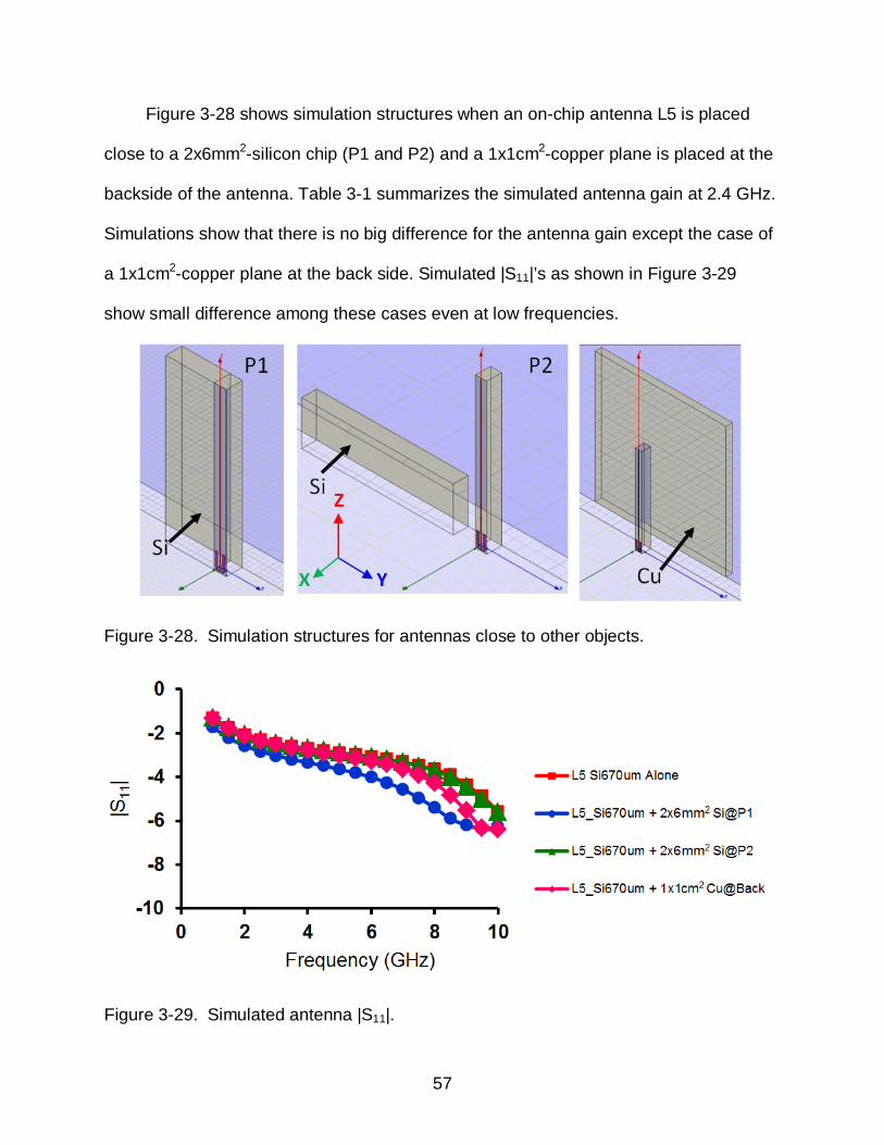
Figure 3-28 shows simulation structures when an on-chip antenna L5 is placed
close to a 2x6mm2-silicon chip (P1 and P2) and a 1x1cm2-copper plane is placed at the
backside of the antenna. Table 3-1 summarizes the simulated antenna gain at 2.4 GHz.
Simulations show that there is no big difference for the antenna gain except the case of
a 1x1cm2-copper plane at the back side. Simulated |S11|’s as shown in Figure 3-29
show small difference among these cases even at low frequencies.
Figure 3-28. Simulation structures for antennas close to other objects.
Figure 3-29. Simulated antenna |S11|.

58
Table 3-1. Simulation results for antenna gain (-x direction) at 2.4 GHz Condition Simulated gain (dB) at 2.4 GHz
antenna L5 alone -37.5
2x6mm2-Si chip @ P1 -38
2x6mm2-Si chip @ P2 -38.6
1x1cm2-Cu plane @ backside -48.3
Measurements were also performed to compare the sensitivities of on-chip and
off-chip antennas to these external structures. Figure 3-30 shows PCB test structures
with different types of antennas. The PCB size is 1.2x1.2 cm2 with a 1.2x0.6cm2-copper
portion as the ground plane and an antenna feed. A 2x4mm2-silicon chip is placed at
different positions near the antenna as shown in the figures. For the P1 and P3 cases,
the silicon chip touches the antenna while there is a gap of ~1 mm between the silicon
chip and the antenna for the P2 case. In the P4 case, only a 1x1cm2-copper PCB is
attached at the back side of antenna.
Figures 3-31 to 3-34 show measured |S11| for off-chip antennas, PCB antennas,
on-chip antennas mounted on a glass slide and on-chip antennas mounted on a PCB,
respectively. For off-chip and PCB antennas, the figures plot only the frequency ranges
at which the input impedances of these antennas are tuned. Measured results show that
the input impedances of on-chip antennas are far less sensitive to the surrounding
objects than those of off-chip and PCB antennas. Specifically, when a 1x1cm2-copper
PCB is placed at the back side, |S11|’s of both off-chip and PCB antennas significantly
change while those for on-chip antennas do not vary much. Figures 3-33 and 3-34 show
that |S11|’s of on-chip antennas vary only ~1.5 dB when the antennas are mounted on

59
different materials. Furthermore, it is clear that when the silicon chip touches the
antenna body, it significantly affects the input matching of both off-chip and PCB
antennas while it slightly changes |S11|’s of on-chip antennas by ~0.5-1 dB.
Figure 3-30. Test structures for different types of antennas and surrounding objects.
Figure 3-31. Measured |S11| for off-chip antennas.

60
Figure 3-32. Measured |S11| for PCB antennas.
Figure 3-33. Measured |S11| for on-chip antennas mounted on glass slides.

61
Figure 3-34. Measured |S11| for on-chip antennas mounted on PCB’s.
The antenna pair gain, Ga, with near-by objects is also of great interest. Figures 3-
35 and 3-36 show the measured Ga’s at 2.4 GHz for both off-chip and on-chip antennas,
respectively. Measurements show that when the silicon chip touches the antenna
structure (P1) which is the most extreme case for a small-form factor, Ga’s of the on-
chip antennas only vary by ~0.2-0.5 dB, while those of the off-chip antennas degrade by
~15-20 dB. Furthermore, Ga’s of the off-chip antenna are almost similar to that of the
on-chip antenna for the P1 case. These show that on-chip antennas are less sensitive
to surrounding objects than off-chip antennas. Therefore, although the performance of
off-chip antennas is better than that of on-chip antennas in ideal cases, both antennas
can exhibit similar performances when the small-form factor requirement is considered.

62
Figure 3-35. Measured Ga for off-chip antennas with surrounding objects at 2.4 GHz.
Figure 3-36. Measured Ga for on-chip antennas with surrounding objects at 2.4 GHz.

63
On-Chip Antenna for µNode Operating at 2.4 GHz
This section presents the suggestion of an on-chip antenna that can be used for
µNode based on HFSSTM simulations. From the µNode link margin analysis in Chapter
2 (table 2-1), the required antenna gain for a communication distance of 20 m at 2.4
GHz while still achieving link margin of 13 dB is greater than -14 dB. This can be
satisfied by employing an on-chip antenna L1 (L=10 mm, W=0, S=0.5 mm) on a 1-cm
diameter battery, thinning the silicon substrate to 100 µm and encapsulating the
antenna with the dielectric material (dielectric constant=4). Figure 3-37 shows the
suggested structure and its simulated input impedance for both real and imaginary
parts. Note that a 2x4-mm2 silicon chip is also considered representing the practical
situation in the real µNode package. At 2.4 GHz, simulations suggest that this antenna
structure achieves gain of > -13 dB as shown in Figure 3-38 and still has reasonable
input impedance for matching network (Zin=22.4-58.3j Ω). Base on this, it is possible to
form a wireless communication link at 2.4 GHz with a useful distance by using a pair of
1-cm on-chip antennas packaged inside µNodes.
Figure 3-37. On-chip antenna for µNode, and simulated |S11|.

64
Figure 3-38. Simulated antenna gain.
Summary
The feasibility of using on-chip antennas in µNode system is studied by antenna
simulations and measurements at varying frequencies. Although the performance of an
on-chip antenna is not as good as that of an off-chip antenna, its size is more compact
and it does not require a large ground plane or keep out area. Furthermore, when the
small-form factor and a nearby silicon chip are considered, the performance of off-chip
and on-chip antennas becomes closer. Finally, simulations suggest that it is possible to
form a wireless communication link at a useful distance by using a pair of 1-cm on-chip
monopoles packaged inside µNodes.

65
CHAPTER 4 THE WIRELESS SWITCH DESIGN FOR µNODE SYSTEM
µNode systems require post fabrication calibration [15]. This requires an ability to
turn the battery power on and off to store the system before and after calibration.
Besides adding another component, since the form factor is small, it is difficult to place
a mechanical switch that can be easily turned on and off. This requirement can be
satisfied by incorporating a wireless switch or a wake-up receiver. Several approaches
have been reported for wake-up receivers [49]-[51]. For this application, a passive RFID
(Radio Frequency Identification) architecture is chosen for no standby power
consumption. To keep the chip area and system size overheads small, the wireless
switch function should share as much of the infrastructure for the main receiver, while
not significantly affecting its performance. This chapter shows an approach for
designing and integrating a wireless switch into a single chip radio, which includes a
circuit that protects against RF signals with an amplitude higher than the normal range.
Wireless Switch Operating Range
The operating frequency of the wireless switch is chosen to be different from the
main transceiver to prevent the loading effect of each other. In this design, the operating
frequency of the wireless switch is 5.8 GHz. The operating range of the wireless switch
can be estimated using the equivalent models as shown in Figure 4-1.
fRF, Ps
Vout, DCRectifier
Rs, Gr, AeRs, Gt, Ae
S
Distance (cm)GPA
Rin
PEIRP
Pt Pr
Vin, RF
RS Rin
VS
Vin, RFPr
Figure 4-1. Operating range estimation for wireless switch.

66
At the transmitter side, the effective isotropic radiated power, PEIRP, is equal to
tPASttEIRP GGPGPP ⋅⋅=⋅= , (4-1)
where Ps, Pt, GPA, Gt are source power, transmitted power, gain of the power amplifier
and the gain of the transmitting antenna, respectively. Hence, the power density is
24 dPS EIRP
⋅⋅=
π, (4-2)
where d is the distance between the transmitting and receiving antennas. At the
receiver side, the received or available power, Pr or Pav, transferred to the matched load
depends on the incident power density, S, and the effective aperture, Ae of the receiving
antenna
22
2 444
⋅⋅⋅⋅⋅=
⋅⋅
⋅
⋅⋅=⋅==
dGGPG
dPASPP rtt
rEIRPeavr π
λπ
λπ
, (4-3)
where the effective aperture is directly related to the wavelength and the gain of the
receiving antenna. This equation is also known as “Friis Equation” [22], [23]. The
amplitude of equivalent source, Vs_peak, and input RF signal, Vin,RF_peak, are equal to
eSavSpeakS ASRPRV ⋅⋅⋅⋅=⋅⋅⋅= 2222_ , (4-4)
Sin
inavS
Sin
inpeakSpeakRFin RR
RPR
RRR
VV+
⋅⋅⋅⋅=+
⋅= 22__, , (4-5)
where Rs and Rin are the antenna and rectifier input impedance respectively. The input
impedance of rectifier is assumed real for simplicity in this estimation. It is clear that in
order to increase the amplitude of input RF signal for fixed available power, the
condition of power match (Rin=Rs) at higher value is preferred. However, typical Rin is
much larger than Rs, therefore the matching network is necessary for the impedance

67
transformation from Rs to Rin. The detail about the impedance transformation will be
discussed in the circuit designs section.
To calculate the required input power to the wireless switch, the power drawn by
the load at the rectifier output needs to be determined. Typical power consumption for
the baseband circuits especially for an RFID system is ~1-2 µW [24], [25]. For this
particular application the power requirement is expected to be much smaller due to the
simpler circuit and the power requirement for the load is set to 1 µW. Assuming the total
power efficiency of the rectifier including the loss from the matching network is 1 % in
the worst case, the received or available power at the receiver side must be equal to
100 µW or -10 dBm. Form the Federal Communication Commission (FCC) rules, the
maximum PEIRP for point to multiple points communication at 5.8 GHz is 4 W or 36 dBm
[26], and the relationship between the operating distance and the receiving antenna
gain is
⋅++=
dGdBmP GHz
rr πλ
4log2036 8.5@ , (4-6)
where λ is the wavelength at 5.8 GHz which is equal to 5.172 cm and Gr is the receiving
antenna gain. Therefore, if the antenna gain is as small as -10 dBi for an on-chip
antenna, the operating range for -10-dBm received power is ~26 cm. The corresponding
input amplitude for the rectifier, Vin,RF_peak, assuming that Rin >> RS is ~200 mV where
RS=50 Ω. For the matching network with quality factor (Q) > 4, the signal amplitude is
amplified so that it can turn on the diodes in the rectifier circuit.
Wireless Switch Architecture
Figure 4-2 shows the architecture of µNode system including a wireless switch.
The wireless switch and main transceiver share the same antenna to reduce the system

68
overhead. The switch is placed in between the antenna and main transceiver since no
signal is available to turn on the T/R (Transmit/Receive) switch and main transceiver for
TDD (Time Division Duplex) operation before the power-up operation is completed. The
wireless switch can load the input of main transceiver, if the wireless switch has 50-Ω
input impedance at the tuned frequency of main transceiver. This addition will cause the
antenna to be mismatched to the transceiver. A way to mitigate this is making the
wireless switch and main radio operate at two different frequencies while utilizing an
antenna that can operate at both frequency bands. More specifically, operating
frequency of 5.8 GHz is chosen for the wireless switch and 2.4 GHz for the transceiver.
Several dual-band antennas have already been reported [52]-[55]. These antennas
provide excellent performance, i.e. gain > 0 dBi for both frequency bands as well as
being compact. The impedance looking into the wireless switch should be high at 2.4
GHz, while the impedance looking into the main transceiver should be high at 5.8 GHz
in order to reduce the impact on each other.
Figure 4-2. Architecture of µNode system.

69
Figure 4-3 shows a simplified schematic of wireless switch for this µNode system.
It is similar to that for a passive transponder in an RFID system. This subsystem
consists of a matching network, an RF clamp, an RF-to-DC converter, a limiter, a
power-on-reset circuit (POR), an envelope detector, a comparator/control logic and a
power switch to turn on the battery. The comparator/control logic and the power switch
are not included in this work. The wireless switch receives energy through the antenna
and converts to DC using an RF-to-DC converter. The envelope detector has been used
to recover the coded signal for authentication of the power-up signal [56]. The
comparator/control logic provides a power-up signal for the power switch to turn the
battery on for the main transceiver. The power switch includes a latch that holds its on-
state after receiving the power-up signal. This means once the main transceiver is
turned on, the power-up signal is no longer needed. For turning the transceiver off, the
2.4-GHz radio link is used. The details of wireless switch are described in the circuit
designs section.
Figure 4-3. Simplified schematic for wireless switch in µNode system.

70
To evaluate the performance of wireless switch as well as its impact on the
transceiver performance, the wireless switch is integrated with a T/R switch. By
evaluating the performance of T/R switch with and without the wireless switch, the
expected impact of wireless switch on the transceiver is estimated. As a matter of fact, if
the receiver, transmitter and antenna are all matched to 50 Ω at 2.4 GHz, the insertion
loss degradation of a T/R switch after integrating a wireless switch will be exactly the
gain and noise figure degradation of the receiver and the output power degradation of
the transmitter. This approach by removing the need for a full transceiver greatly
simplifies the task of quantifying the impact of wireless switch.
Operation Modes
Operation range of transceiver is a key design target. For the RF power-up and
down applications, the range of wireless switch circuit can be significantly shorter (less
than 10 cm) than that of the main transceiver. Therefore, operating frequency of 5.8
GHz with higher propagation loss is chosen for the wireless switch. The operation
modes (power-up (PUx) and transceiver (TRx) modes) for a matching network of
wireless switch are shown in Figure 4-4.
In PUx mode, the main transceiver is turned off, thus its input impedance looking
at the input of the T/R switch, is high. The matching network of wireless switch is
designed so that its input impedance is 50 Ω at 5.8 GHz. Therefore, essentially all the
available power of RF power-up signal at 5.8 GHz picked up by the antenna is delivered
to the wireless switch.
In TRx mode, the main transceiver is turned on and the RF signal frequency is 2.4
GHz. The input impedance of wireless switch is close to open at 2.4 GHz. Therefore,
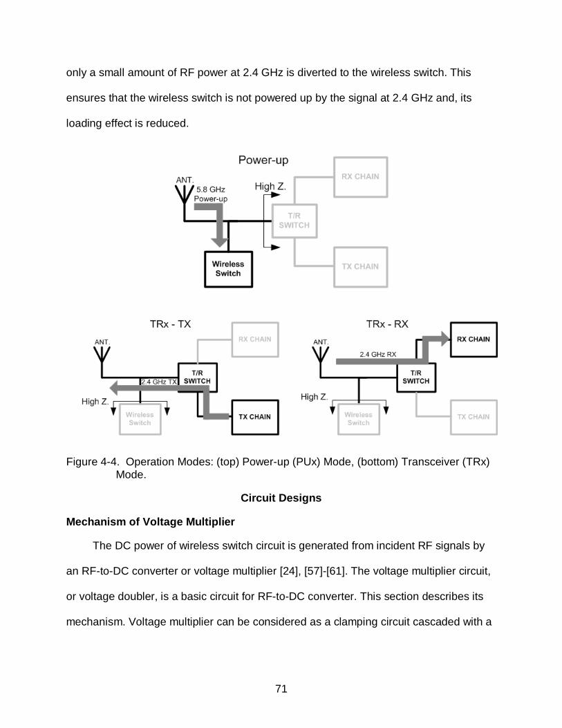
71
only a small amount of RF power at 2.4 GHz is diverted to the wireless switch. This
ensures that the wireless switch is not powered up by the signal at 2.4 GHz and, its
loading effect is reduced.
Figure 4-4. Operation Modes: (top) Power-up (PUx) Mode, (bottom) Transceiver (TRx) Mode.
Circuit Designs
Mechanism of Voltage Multiplier
The DC power of wireless switch circuit is generated from incident RF signals by
an RF-to-DC converter or voltage multiplier [24], [57]-[61]. The voltage multiplier circuit,
or voltage doubler, is a basic circuit for RF-to-DC converter. This section describes its
mechanism. Voltage multiplier can be considered as a clamping circuit cascaded with a

72
rectifier circuit as shown in Figure 4-5. To ease the analysis for the mechanism of
voltage multiplier, some conditions are assumed:
1. The diode must turn “on” if VD=Vanode - Vcathode > 0 and “off” if VD < 0. Also, the
current flow in diode is analogous to the water flow in a water pipe with a valve that
allows one direction of current flow. In another word, only positive charges flow from an
anode to a cathode or negative charges flow from a cathode to an anode is allowed.
2. The initial conditions across all capacitors are zero. All capacitors have the
same value. Also, these capacitors can be treated as “short circuits” for an AC signal
and as “opened circuits” for DC signal.
+Vout
-
+
RF Input
- Clamping Rectifier
D2C1 VX
D1 C2
Figure 4-5. Voltage multiplier or voltage doubler circuit.
The analysis is further simplified when it starts with a negative cycle of the RF
input signal. Figure 4-6 shows the voltage multiplication mechanism. Starting with the
negative part of the input signal during time t0-t1, the input source starts to deposit more
negative charges though the capacitor C1 causing diode D1 and D2 to turn “on” and “off”,
respectively. This makes the voltage at node Vx=0 and, also, leaves the voltage at node
Vout=0 as shown in case (a) of Figure 4-6. During time t1-t3, the input signal starts to turn
back to positive side, thus more positive charges are deposited through the capacitor

73
C1. This causes diode D1 to turn “off” and diode D2 to turn “on”. The circuit forms a
capacitive divider between C1 and C2 (where C1=C2) as shown in case (b). Therefore,
the voltage at nodes Vx and Vout are equal and both of them track the input signal with a
divide ratio of 0.5 to reach the final value, Vp, at time t3. After reaching its peak value,
Vp, the input signal starts to fall back to zero and deposits more negative charges
through capacitor C1 during time t3-t4. This makes diodes D1 and D2 turn “on” and “off”
as shown in case (c), respectively. The voltage at node Vx follows the input signal to
zero but that of the node Vout will hold at Vp because diode D2 is off. For the following
cycle, the mechanism during time t4-t5 is the same as that of the time t0-t1 as shown in
case (d). During time t5-t6, although the input signal starts to deposit positive charges,
diode D2 cannot turn “on” because Vcathode of D2, (=Vout=Vp), is greater than Vanode of D2,
(=Vx=0). This is shown by case (e). Therefore, the voltage at node Vx just follows the
input signal without any division. At time t6, when the voltage at the node Vx reaches Vp,
this turns diode D2 “on” and the circuit forms a capacitive divider again as shown in case
(f). During the period, t6-t7, the voltage at node Vx follows the input signal with the same
divide ratio, 0.5 but the period is shorter than that for the case (b). Therefore, the
voltage at nodes Vx and Vout reaches Vp+Vp/2 at time t7. The same process as in case (c)
starts over again during time t7-t8 for case (g). The mechanism of the voltage multiplier
repeats itself again for other cycles but the output continues to rise by Vp/4, Vp/8, Vp/16
and etc., in each input cycle, approaching the final value of
ppppp
pfinalout VVVVV
VV ⋅=
−=
+++=+++= 2
211
1...41
211...
42, . (4-7)

74
VX
RF Input
Vout
VP
-VP
VP
VP/2
VP
VP/2
t1 t2 t3 t4 t5 t6 t7 t8t0
D2C1
VX
D1 C2
a) t0-t1
D2C1
VX
D1 C2
b) t1-t3
D2C1
VX
D1 C2
c) t3-t4
D2C1
VX
D1 C2
d) t4-t5
D2C1
VX
D1 C2
e) t5-t6
D2C1
VX
D1 C2
f) t6-t7
D2C1
VX
D1 C2
g) t7-t8
Figure 4-6. Mechanism of voltage multiplier circuit.
Radio Frequency-to-Direct Current Component (RF-to-DC) Converter
Figure 4-7 shows the RF-to-DC converter integrated with an impedance trans-
formation network. The DC voltage generated at the converter output is approximately
equal to [24]
( )fwdpeakInRFDC VVNV −⋅≈ , , (4-8)
where N is the number of diodes, VIn RF, peak is the amplitude of input RF signal as shown
in Figure 4-7 and Vfwd is the forward bias voltage of diodes. A critical figure of merit for
this circuit is the power conversion efficiency [57], [60],
inRF
DCc P
P
,
=η, (4-9)
inRFP , = Incident RF Power - Reflected RF Power = )1( 211, SP AvailRF −⋅ , (4-10)

75
where PDC is the DC power measured at the output of the converter, PRF,Avail is the
available power provided by the input source, |S11| is the input return loss and PRF,in is
the power delivered into the RF-to-DC converter.
The required RF input power should be as small as possible for longer operating
range. This requires low power consumption circuits connected at the converter output
and high input impedance (Zi in Figure 4-7) which further reduces the required RF input
power by increasing the conversion efficiency. Typical power consumption of an RFID
baseband circuit is on the order of ~1-2 µW [24], [25]. Since the function of baseband
for the wireless switch is much simpler than that of an RFID, its power consumption
should be significantly lower.
Figure 4-7. The radio frequency-to-direct current component (RF-to-DC) converter with a matching network.
76
Ideally, the highest efficiency is achieved with a single stage. However, generation
of sufficiently high DC output voltage with only one stage requires large input voltage
amplitude and, hence, a high-Q matching network to transform the antenna impedance
which is typically around 50 Ω. To relax this, multiple stages are needed. In this wireless
switch design, an RF-to-DC converter with 5 stages is chosen. To achieve high Q, an
on-chip metal-oxide-metal capacitor, Cseries and a bond wire inductor, Lshunt are used for
matching shown in Figure 4-7. A concern for a bond wire inductor is its variations. The
length of bond wire inductor can be controlled within ~±50 µm. With the variations of
bond wire inductor and on-chip capacitor, the tuning frequency is expected to vary
~±100 MHz and |S11| at 5.8 GHz is expected to be less than -10 dB over these
variations. An on-chip inductor with lower Q can also be used at the expense of more
loss and degraded efficiency. Since for the applications of interest, the range and
transmitted power can be selected with a great deal of flexibility, the degradation of
efficiency can be tolerated.
The diode sizing along with the number of stages for the RF-to-DC converter also
needs to be considered to improve the efficiency. Since diodes with higher saturation
current, a lower forward bias voltage drop and faster switching time are desirable for
better efficiency, Schottky Barrier diodes (SBD’s) have been chosen [24], [58]. These
SBD’s are created without process modifications by using the layout layers available in
the standard design kit [62]-[64]. In this design, SBD’s with measured characteristics
have been used to optimize the power efficiency. Figure 4-8 shows an n-type Schottky
Barrier diode layout and its cross section and Figure 4-9 shows an equivalent model
including parasitics. An n-well-to-p-substrate diode, Dnwell-sub, has been added to

77
account its junction breakdown. Because the operating frequency of RF-to-DC
converter (5.8 GHz) is low compared to the cut-off frequency of diode, the main trade-
off for sizing the diodes is between increasing the saturation current which leads to
higher direct current slope and higher DC output voltage, and decreasing n-well-to-
substrate parasitics which introduces loss and degrades efficiency. A single diode cell
with a larger area that has a smaller n-well to Schottky diode area ratio should be better
than a structure with multiple minimum area diode cells connected in parallel.
For the series resistance Rs, it includes all the resistances between the Schottky
Barrier contact and ohmic contact. The series resistance Rs [64] is
( ) Cs
nsas
STIshs
jSTInwellsh
nwellsh
CS
Rll
lRllR
lxd
RR
RRRRR
+
+
+
+
⋅+≈
+++≈
+−−−−
1
212
321
22429, (4-11)
where Rsh-nwell is the n-well sheet resistance, Rsh-STI is the n-well sheet resistance under
the shallow trench isolation (STI), Rsa-n+ is the salicided n+ sheet resistance, Rc is the
resistance associated with the contacts and vias. ls is the length of the Schottky, l1 is the
STI width and l2 is the separation between the edge of STI and n-well metal contact. dSTI
is the STI thickness and xJ is the n-well depth.
For the junction capacitance for SBD, its expression is similar to that a p-n diode.
The difference is that SBD does not have diffusion capacitance when it is forward
biased because the minority-charge storage effect is not present [65]. This capacitance
can be expressed as
jm
bi
joj
VV
CC
−
=
1 , (4-12)

78
21
2
2
=
bi
siDsjo V
qNlC
ε , (4-13)
where Cjo is the zero bias junction capacitance, q is the charge of an electron, ND is the
n-well doping density, εsi is the permittivity of silicon, Vbi is the built-in potential and mj is
the junction grading coefficient.
Figure 4-8. N-type Schottky barrier diode layout and its cross section.
Figure 4-9. Diode equivalent model with associated parasitics.

79
Figure 4-10 plots the current-voltage characteristics of three measured SBDs in
130nm digital CMOS process. The Schottky areas are also listed in the figure. Figure 4-
11 plots the simulation results for the power efficiency of 5-stage RF-to-DC converters
constructed with these diodes. Simulations shows that a Schottky diode with a unit area
of 1.28x1.28 µm2 and the corresponding n-well size of 4.88x3.24 µm2, and the space
between the Schottky contact and n+ diffusion of 1.16 µm is better suited. The Rs and Cj
of this diode is ~84 Ω and ~5 fF, respectively. This diode also gives corresponding n-
well parasitic capacitance and resistance of ~10.8 fF and ~105 Ω, respectively.
Figure 4-10. Current-voltage characteristics of measured Schottky Barrier Diodes.
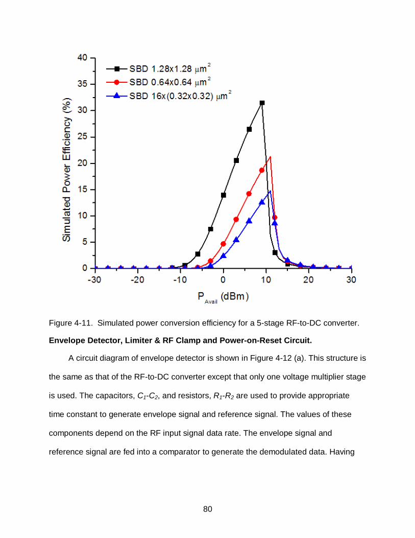
80
Figure 4-11. Simulated power conversion efficiency for a 5-stage RF-to-DC converter.
Envelope Detector, Limiter & RF Clamp and Power-on-Reset Circuit.
A circuit diagram of envelope detector is shown in Figure 4-12 (a). This structure is
the same as that of the RF-to-DC converter except that only one voltage multiplier stage
is used. The capacitors, C1-C2, and resistors, R1-R2 are used to provide appropriate
time constant to generate envelope signal and reference signal. The values of these
components depend on the RF input signal data rate. The envelope signal and
reference signal are fed into a comparator to generate the demodulated data. Having

81
the reference signal enables proper operation even when the envelope signal does not
swing down all the way to zero.
The DC output voltage as well as input voltage of RF-to-DC converter can be
unacceptably high. This can damage the converter and circuit connected to its output.
To prevent this, a limiter and RF clamp shown in Figure 4-12 (b) have been included.
The locations of these elements in the transceiver are shown in Figure 4-3.
Figure 4-12. Sub-circuits for Wireless Switch: (a) Envelope detector circuit. (b) Limiter and RF clamp. (c) Power-on-Reset circuit. (d) Simplified transmit/receive (T/R) switch schematic.

82
The limiter consists of 3 p+-to-n‐well diodes connected in series at the output of
RF-to‐DC converter. The RF clamp consisting of a p+-to-n-well diode and an n+-to-p-
substrate diode in an anti‐parallel configuration is connected to the antenna port. The
junction areas of p+-to-n-well and n+-to-p-substrate diodes are 100 µm2. The total
parasitic capacitance of the RF clamp is ~110 fF. Once the DC output voltage is higher
than 3vd,p+, (where vd,p+ is the turn-on voltage of p+-to-n-well diodes), the diodes turn on
and limit the DC output voltage. For the RF input signal with amplitude greater than vd,p+
for positive side and vd,n+ (where vd,n+ is the turn-on voltage for the n+-to-p-substrate
diode) for negative side, the clamp turns on and limits the input signal level.
The power-on-reset circuit for the wireless switch is shown in Figure 4-12 (c). It is
composed of a cross-coupled pair of NMOS transistors and a NOR gate [56]. When the
DC output voltage from the RF-to-DC converter is sufficiently high, one branch of the
cross-coupled pair over powers the other and latches the value. Long channel devices
that increase the gain of inverters [66], and damping capacitor, C, [56] are used to
reduce the probability of cross-coupled pair being in a meta-stable state. The NOR gate
compares the two signals and generates a pulse (power-on-reset signal) to initialize a
logic block (not included) that determines whether the rest of circuits should be powered
up.
Transmit/Receive (T/R) Switch for µNode Transceiver
To evaluate the performance of wireless switch and transceiver in the presence of
the other, a T/R switch for TDD communication system is connected to the wireless
switch. Figure 4-12 (d) shows a simplified schematic of a broad band T/R switch. The
T/R switch [67] achieves insertion loss of ~0.7 dB, return loss of ~20 dB and isolation

83
greater than 30 dB at 2.4 GHz. To combine the wireless switch and transceiver chain
together, as mentioned in section III, the input impedance looking into the wireless
switch must be high at 2.4 GHz to prevent loading, while matched at 5.8 GHz. This is
realized by using the same shunt inductor and series capacitor input matching network
that transforms 50 Ω to higher input impedance of the RF-to-DC converter as shown in
Figure 4-7. The series capacitor, Cs, increases the input impedance at 2.4 GHz to
reduce the loading of converter. Figure 4-13 shows the frequency dependence of input
impedance for the entire system on a Smith chart in both PUx and TRx modes.
Figure 4-13. Input impedance of the entire system for both operating modes: Power-up (PUx) and Transceiver (TRx) modes, (design targets and measurement results).

84
In PUx mode, the T/R switch is turned off so its input impedance is capacitive and
high. Since the matching circuit of wireless switch is tuned at 5.8 GHz, the total input
impedance is at the center of Smith chart (X2) and at the lower-right-hand side at 2.4
GHz (X1). In TRx mode, due to the broad band response of T/R switch, its input
impedance is ~50 Ω at both 2.4 and 5.8 GHz. Because the input matching network of
wireless switch is high impedance at 2.4 GHz and matched to 50 Ω at 5.8 GHz, the total
impedance seen by the receiver input and transmitter output is 50 Ω (X4) at 2.4 GHz
and 25 Ω (X3) at 5.8 GHz.
Experimental Results
A die micrograph for an integrated circuit including both wireless switch and T/R
switch is shown in Figure 4-14. The chip size is ~1400x730 µm2 including bond pads.
The area of the wireless switch excluding bond pads is ~400x590 µm2.
Figure 4-14. Chip die micrograph.

85
This circuit is fabricated in a 130-nm digital CMOS process. The wireless switch
and T/R switch are connected on-chip for characterization of the T/R switch and
wireless switch combination. More specifically, the antenna bond pads of T/R switch
and input bond pads of wireless switch are connected at the center of the chip. The
bond pads on the wireless switch side, including a ground pad, are used to make the
bond wire connections for Lshunt in Figure 4-7. These bond pads in combination with
laser cuts also allow separate characterization of the RF-to-DC converter with and
without a matching network, and the T/R switch by itself.
The input return loss, DC output voltage and the power conversion efficiency of
RF-to-DC converter are measured. A 1-MΩ load off-chip is connected at the output of
the converter. Figures 4-15 and 4-16 show the measured small-signal and large-signal
|S11|’s of the converter with the matching network, respectively.
Figure 4-15. Small-signal |S11| of the RF-to-DC converter with a matching network.
In Figure 4-15, the matching network is tuned at ~5.7 GHz. The input impedance
is high at 2.4 GHz. The resonant frequency is slightly below the target, because of
errors in modeling the matching network and the previously discussed variations of the

86
passive components. The large-signal |S11|, DC output voltage and the power
conversion efficiency (also for the case without matching network) are measured at this
tuned frequency. Figure 4-16 shows that |S11| is below -10 dB for input power less than
~-12 dBm and over than -10 dB for input power greater than -10 dBm. This high |S11| at
higher input RF power level is not a serious issue since the power level is already large
enough to turn on the wireless switch although the return loss is high.
Figure 4-16. Large-signal |S11| of the RF-to-DC converter with matching network at 5.7 GHz.
Figures 4-17 and 4-18 show measured and simulated DC output voltage and
power conversion efficiency of the RF-to-DC converter (with and without a matching
network), respectively. The limiter at the output was laser cut for these measurements.
The power efficiency is calculated using equations (4-9) and (4-10). These two figures
are plotted versus the available power, PAvail, of an external RF signal generator.

87
Figure 4-17. DC output voltage vs. available power, PAvail.
Figure 4-18. Power conversion efficiency vs. available power, PAvail.

88
In Figure 4-17, at the same PAvail ~-13 dBm, the converter with a matching network
generates DC output voltage of around 1 V instead of ~0 V for the converter without the
matching network. This clearly demonstrates that the matching network improves the
sensitivity of wireless switch. The measurements also agree well with the simulation
results overlaid in the same figures. At high available power levels, the DC output
voltage saturates around 10 V because of the breakdown voltage associated with the n-
well to p-substrate junction of Schottky diodes. When the limiter circuit is connected, the
DC output voltage of the converter is clamped at 3vd,p+ (~2 V), where vd,p+ is the turn-on
voltage for the p+-to-n-well diode. The efficiency peaks and falls beyond a certain input
power level due to the n-well-to-substrate junction breakdown that saturates the output
voltage. At PAvail < 0 dBm, the converter with the matching network provides higher
conversion efficiency. However, its efficiency increases at a slower rate than the one
without the network and reaches the maximum of around 14 % at PAvail of ~0 dBm while
the converter without the matching network shows the peak efficiency of around 34 % at
PAvail ~9 dBm. The degradation of power conversion efficiency is due to the loss of the
matching network resulting from the finite Q of on-chip capacitor and bond wire
(estimated Q of ~50 at 5.8 GHz). The measured and simulated results agree well.
For the T/R switch characterization, since only a small battery with supply voltage
of 1.2 V is expected to be available in µNodes, the DC bias voltage (VBias) for the shunt
transistors of the switch has been connected to ground instead of 1.8 V [67]. Figure 4-
19 shows the measured performance of the T/R switch alone. At 2.4 GHz, the T/R
switch has 0.7-dB insertion loss, around 24-dB isolation (from antenna port to TX or RX
port) and less than -15 dB |S11| and |S22|.

89
Figure 4-19. Measured performance of T/R switch.
Figure 4-13 also shows the measured input impedance of wireless switch
integrated with the T/R switch at both PUx and TRx modes. In PUx mode, the input
impedance is capacitive at 2.4 GHz, (marker m1) and close to the center of Smith chart
at 6.28 GHz, (marker m2). There is a frequency shift from 5.7 to 6.28 GHz. This is due
to the difference of position for the RF probe compared to that for the RF-to-DC
converter measurement alone (Figure 4-14). The probe is much closer to the bond wire,
and the mutual coupling with the probe reduces the effective length of bond wire,
increasing the tuning frequency from 5.7 to 6.28 GHz. In the actual µNode
implementation, the circuits can be rearranged to reduce this mutual coupling and thus

90
the discrepancy. In TRx mode, when the T/R switch is turned on, the input impedance
of circuit is close to the center of Smith chart at 2.4 GHz, (marker m4), and the input
impedance at 6.28 GHz moves toward the 25-Ω constant resistance circle (marker m3)
due to the broad band response of T/R switch and loading of the wireless switch as
discussed in the previous section.
The performance of T/R switch after integrating the RF wireless switch is shown in
Figures 4-20 and 4-21 for PUx and TRx mode, respectively. In PUx mode, the isolation
from the antenna port to TX or RX port at 2.4 GHz is around 24 dB and |S11| is less than
-11 dB at 6.28 GHz. In TRx mode, at 2.4 GHz, the insertion loss of switch is degraded
by ~0.3 dB to 1 dB, and |S11| and |S22| are less than -10 dB.
Figure 4-20. Measured performance of T/R switch integrated with a wireless switch in Power-up (PUx) mode.

91
Figure 4-21. Measured performance of T/R switch integrated with a wireless switch in Transceiver (TRx) mode.
Figure 4-22. Measured 1-dB compression points of T/R switches with and without a wireless switch.

92
The effect of the wireless switch on the linearity of the T/R switch is also of great
interest. Figure 4-22 shows the measured 1-dB compression point (P1dB) for the T/R
switch with and without the wireless switch. The input referred P1dB of T/R switch
degrades ~0.5 dB when the wireless switch is added due to the RF clamp circuit added
at the antenna port. This also indicates that the RF clamp will limit input power larger
than ~12 dBm to protect the wireless switch and transceiver. These measurement
results show that the deleterious effect of adding a wireless switch into a transceiver
can be adequately managed.
Summary
This chapter presents a dual frequency band approach for integrating a wireless
switch using an RF-to-DC converter (5.8 GHz) with a 2.4-GHz transceiver. The RF-to-
DC converter is the first fully integrated converter operating at 5.8 GHz. The approach is
demonstrated by evaluating the performance impact of adding the wireless switch to a
T/R switch. In a 130-nm digital CMOS process, a T/R switch integrated with the wireless
switch achieves ~0.3 dB higher insertion loss and 0.5-dB lower 1-dB compression point
at 2.4 GHz compared to that without the wireless switch. The maximum power efficiency
of RF-to-DC converter using Schottky diodes and a bond wire inductor for matching or
impedance transformation is 14 % at 5.7 GHz. The maximum occurs when the available
input power is 0 dBm. These indicate that integration of a wireless switch for turning on
and off a transceiver of M&MTM sized or smaller communication nodes by using RF
signals can be accomplished with minimal performance degradation for the transceiver.

93
CHAPTER 5 LOW POWER RECEIVER FRONT-END DESIGN
In a µNode, the power consumption of radio communication subsystem is a
dominant factor determining its size and life time. To lower the overall power
consumption, a low power RF front-end is thus necessary. However, the performance of
system normally depends on power consumption so careful design of the RF front-end
is critical to lower total power consumption while maintaining acceptable system
performance. Several low power radio subsystems have been reported [70]-[74].
However, a phase-locked loop (PLL) and local oscillator (LO) buffers which are the most
power consuming blocks are often not included. Some even use an external LO source
[65], [66] which provide little information on their usefulness in real situations. This
chapter discusses the architecture and circuit design issues for reducing the power
consumption of an RF receiver front-end including LO driver co-optimization.
Figure 5-1. Receiver front-end architecture.
Receiver Front-End Architecture
Fig.5-1 shows the proposed receiver front-end. It is intended for use in low
intermediate frequency (IF) (~1-2 MHz) architecture with reduced block counts, power

94
consumption and chip size. The input matching network boosts the RF voltage level [70]
before down-conversion using single balanced passive mixers. A mixer-first structure
was used to eliminate the power consumption of low noise amplifier (LNA) operating at
the RF frequency. The PLL provides 4-phase LO signals with a 25% duty cycle for
quadrature down-conversion. These non-overlapping LO signals [70], [72], [73] and
voltage gain from the matching network [70] improves overall performance of the
receiver as well as reducing the power consumption of the RF subsystem.
Circuit Designs
This subsection discusses the design issues for the RF front-end. This RF circuit
consists of a ring-oscillator based PLL, impedance transformation network, passive
mixers, baseband amplifiers and a 25%-LO driver. Optimization for this front-end
through simulation is also presented.
Ring-Oscillator Based Phase Locked Loop (PLL)
A circuit schematic of PLL is shown in Figure.5-2 [21]. This circuit is designed by
C.-Y. Cha [21]. With a 50-MHz frequency reference and a divide-by-48 frequency
divider, the PLL generates four 2.4-GHz LO signal phases for the receiver. A 4-stage
ring oscillator with differential outputs was used instead of an LC-based one. Because
the power consumption of a CMOS ring oscillator scales with the total switched
capacitance and square of the supply voltage, its power dissipation drops more rapidly
with the technology scaling and can be even lower than the power consumed by LC-
oscillators [75]. This simultaneously minimizes the power consumption as well as the
chip area. Especially for generation of 4-phase non-overlapping LO signals, this type of
relaxation oscillators is more area efficient than LC oscillators. The loop filter following
the charge pump is designed to set the PLL bandwidth to ~3 MHz. The values of

95
capacitors C1, C2 and the resistor are 0.1 pF, 2 pF and 120 kΩ, respectively. Figure.5-3
shows the oscillator structure [21]. It consists of a V-to-I converter and a 4-stage ring
oscillator. This oscillator can provide up to 8-LO signal phases. However, only the 4
phases are used for the quadrature down conversion in the receiver chain. The
oscillator output buffer drives the frequency divider and interconnect line between the
PLL and 25%-LO driver. The frequency divide-by-48 circuit utilizes conventional current
mode logic (CML) divide-by 2 and 3 circuits and its simulated maximum operating
frequency is ~9 GHz.
Figure 5-2. Charge pump based type-II phase locked loop (PLL) for generating local oscillator (LO) signal.
Figure 5-3. 4-Stage ring oscillator.

96
Impedance Transformation Network
The input impedance transformation network or tapped capacitor resonator is
shown in Figure 5-4. This circuit consists of capacitors (C1 and C2) and shunt inductor
(L1). This circuit has the ability to set the center frequency, quality factor (Q) of the
network, and impedance transformation ratio. To simplify the analysis, some parasitic
capacitance associated with capacitors and inductors are neglected and the inductor is
assumed to have sufficiently high self-resonant frequency (SRF).
C1
C 2Rs
L1
Rout
inv
outvci
Figure 5-4. Tapped capacitor resonator as an impedance transformation network.
To achieve high voltage gain and low noise figure from this network, passive
components with high quality factor, Q, are necessary. However, Q for on-chip inductors
is normally limited by the integrated circuit (IC) process. Careful consideration and
design for passive components are necessary. Assuming that negligible current flows
into the source resistance Rs, the voltage gain of this network can be approximated as
[20]
)1(1
2
CCvv inout +≈ . (5-1)
For a lossless network, the impedance transformation ratio can also be approximated
as

97
sout RCCR 2
1
2 )1( +≈ (5-2)
To better understand the effect of Q on the performance of this circuit, with shunt-to-
series transformation followed by series-to-shunt transformation as shown in Figure 5-5,
the output impedance of the matching network is
ss
out RQQR 2
2
2
11++
= , (5-3)
where ss RC
XRQ 2
22 ω== and
121
1
222
1)()1(CR
CCCCRQ
RXQ
ss
s
ss ω
ω ++=+= , (5-4)
where '21 XXX s = ,
11
1C
Xω
= , '2
'2
1C
Xω
= and ( )222
'2 1 −+= QCC .
Assuming that X2 << RS, the impedance transformation ratio in equation (5-3) is
approximately equal to that in equation (5-2). In order to resonate at the desired
frequency, the output impedance of composite RC network must present an imaginary
part of equal magnitude but opposite sign to that of the inductor at the resonant
frequency. Since the input of this network is connected at the node between C1 and C2,
the parasitic capacitance associated with interconnect lines and additional components
such as a bond pad, a bond wire and etc., must be carefully taken into account. By
using the circuit in Figure 5-5, the resonant frequency of this network is
eqo CL
f12
1π
= , (5-5)
where2
2221
2221
)()1(CQCC
QCCCeq +++
= .

98
Figure 5-5. Transformation of tapped capacitor resonator.
Figure 5-6. Resonant frequency, fo, of tapped capacitor resonator vs. variation of C2.
Figure 5-6 shows a plot of resonant frequency of this resonator versus C2 while C1
and L1 are kept constant. The initial value of C1, C2 and L1 needed to achieve the
resonant frequency of 2.4 GHz are 340 fF, 320 fF and 13.5 nH, respectively. Note that
these are not the actual values used in real design since additional parasitics
associated with passive components and interconnect lines must be included in the final
design. This plot shows that the resonant frequency of this tapped capacitor resonator is

99
relatively insensitive to the variation of C2. This is one of the major advantages of this
transformation network and simplifies the design.
The noise contribution of this network is mostly from both source resistance Rs
and series resistance RL associated with the shunt inductor L1 (not shown in Figures 5-4
and 5-5). To achieve a low noise factor, the total output noise due to RL should be
minimized, or high QL is desirable. The relationship between the noise factor of this
network and quality factor of the passive component can be considered by using the
shunt-to-series transformation for RL and assuming 1,1 22
2 >>>> QQs and 12 >>LQ . Under
this set of assumptions, the noise factor of can be approximated as
L
s
LL
ss
LL
sS
LL
ss
QRQX
QRQQR
QRQQR
factorNoise +=+≈
+≈+
++
+= 111)1(
11
1 22
2
22
22
2
, (5-6)
where |Xs|=|XL| at the resonant frequency.
This analysis clearly shows that high quality factor of inductor, QL improves the
noise performance. When matched, QL=Qs and the noise factor from (5-6) is equal to 2
(or 3-dB noise figure). However, in actual design, Qs can be made less than QL to
reduce the noise performance while trading some voltage gain due to the mismatch.
Simulated performance of this matching network with varied QL is shown in Figures 5-7
and 5-8. In this design, the impedance is transformed from 50-Ω RS to 1-kΩ Rout. From
these simulations, high QL is desirable for this kind of matching network because it
gives lower noise factor (or noise figure), and higher voltage gain. However, high Q for
on-chip components, especially for the inductor, is difficult to achieve. Therefore, other
types of inductors with higher Q such as bond wire or off-chip inductors were used to
improve the performance of this matching network.

100
Figure 5-7. Simulated performance of matching network with varying QL: noise figure and voltage gain.
Figure 5-8. Simulated performance of matching network with various QL: |S11| and |S22|, (|S22| is normalized with 1-kΩ source resistance).

101
Passive Mixers
In this proposed radio, only one mixer performs frequency translation from RF to
baseband or low IF. Therefore, the mixer is directly connected to the output of
impedance transformation network. The passive mixer has been chosen in this design
due to its high linearity, no dc power consumption and low flicker noise [71], [76]. This
subsection describes the design of passive mixer.
A single-balanced passive mixer has been chosen over a double-balanced
passive mixer because the former requires a fewer number of LO drivers reducing
power consumption and has 6-dB higher conversion gain than that of the double-
balanced passive mixer [71]. The circuit schematic and the small-signal equivalent
circuit for a single-balanced passive mixer are shown in Figure 5-9. The circuit consists
of two switching transistors (M1-M2), input capacitor (Cin), bias resistors (RBias), LO ac-
coupling capacitors (CLO) and load capacitors (CL). The LO ac-coupling capacitors are
added to prevent low frequency noise flowing into the gates of switching transistors and
to provide the flexibility for gate bias. VCM and VBias at the gate set the bias of the
transistors. In the equivalent models, the switching transistors are modeled as switches
and Ron is the on-resistance of the switching transistors. Ø1 and Ø2 are non-overlapping
LO driving signals.
To analyze the voltage conversion gain at 0-Hz offset, the square wave
approximation for the conductance of switching transistors is used as shown in Figure
5-10 [70], [71]. The RF input consists of both in-phase and quadrature-phase
components. Multiplying the normalized RF input with the mixing pulse, (+1, -1), the
voltage conversion gain is the difference voltage stored at node VC1 and VC2 where the
voltage at each node is simply the average of the normalized input while the switch is

102
conducting. When the switch is conducting the output voltage is the sampled value of
the normalized input, and the capacitance CL holds the output when the switch is off.
Also, note that the quadrature-phase input produces a zero output. Therefore, the gain
can be calculated by ignoring the quadrature components and it can be expressed as
∫∫ ∫−−
+
−
==
−=−=
D
D
D
D
D
DCCgleconv D
DdD
ddD
VVGπ
π
π
π
ππ
ππ ππθθ
πθθθθ
πsin2cos1coscos
21
21sin, , (5-7)
where D is the conduction cycle, 0 < D < 0.5. Compared this conversion gain
expression to that of the double-balanced passive mixer,
DDG doubleconv ππsin
, = , (5-8)
the conversion gain of the single-balanced passive mixer is 2 times or 6 dB higher [70],
[71], [76]. Another way to simply explain this conversion gain difference is that the
double-balanced mixer has differential input and output while the single-balanced mixer
has a differential output but a single-ended input.
Figure 5-9. Schematic and equivalent models for a single-balanced passive mixer.

103
Figure 5-10. Switching conductance with pulse approximation for mixer conversion gain analysis.
The output impedance of single-balanced passive mixer can be calculated by
using the equivalent model shown in Figure 5-11. By calculating the average current, IX,
over a period, the output impedance of the mixer can be expressed as
( ) onS
X
onS
XXavg RR
DVDRR
VdtII+⋅
=⋅
+
⋅== ∫ πππ
π
422
121 2
0
, (5-9)
DRR
IVR onS
avg
Xout
+== , (5-10)
and the mixer output pole formed by Rout and CL is
( ) LonSLoutdB CRR
DCR ⋅+
=⋅
=−1
3ω . (5-11)
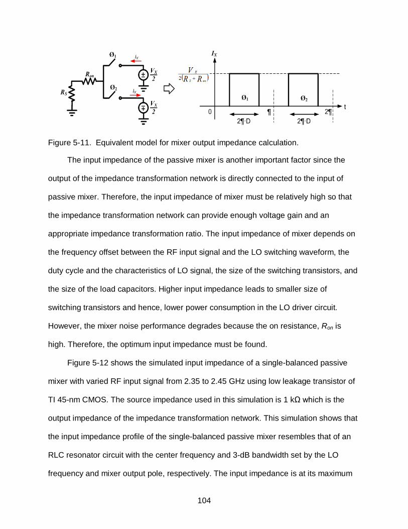
104
Figure 5-11. Equivalent model for mixer output impedance calculation.
The input impedance of the passive mixer is another important factor since the
output of the impedance transformation network is directly connected to the input of
passive mixer. Therefore, the input impedance of mixer must be relatively high so that
the impedance transformation network can provide enough voltage gain and an
appropriate impedance transformation ratio. The input impedance of mixer depends on
the frequency offset between the RF input signal and the LO switching waveform, the
duty cycle and the characteristics of LO signal, the size of the switching transistors, and
the size of the load capacitors. Higher input impedance leads to smaller size of
switching transistors and hence, lower power consumption in the LO driver circuit.
However, the mixer noise performance degrades because the on resistance, Ron is
high. Therefore, the optimum input impedance must be found.
Figure 5-12 shows the simulated input impedance of a single-balanced passive
mixer with varied RF input signal from 2.35 to 2.45 GHz using low leakage transistor of
TI 45-nm CMOS. The source impedance used in this simulation is 1 kΩ which is the
output impedance of the impedance transformation network. This simulation shows that
the input impedance profile of the single-balanced passive mixer resembles that of an
RLC resonator circuit with the center frequency and 3-dB bandwidth set by the LO
frequency and mixer output pole, respectively. The input impedance is at its maximum
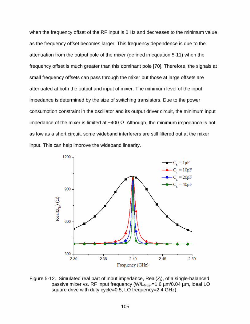
105
when the frequency offset of the RF input is 0 Hz and decreases to the minimum value
as the frequency offset becomes larger. This frequency dependence is due to the
attenuation from the output pole of the mixer (defined in equation 5-11) when the
frequency offset is much greater than this dominant pole [70]. Therefore, the signals at
small frequency offsets can pass through the mixer but those at large offsets are
attenuated at both the output and input of mixer. The minimum level of the input
impedance is determined by the size of switching transistors. Due to the power
consumption constraint in the oscillator and its output driver circuit, the minimum input
impedance of the mixer is limited at ~400 Ω. Although, the minimum impedance is not
as low as a short circuit, some wideband interferers are still filtered out at the mixer
input. This can help improve the wideband linearity.
Figure 5-12. Simulated real part of input impedance, Real(Zi), of a single-balanced passive mixer vs. RF input frequency (W/LMixer=1.6 µm/0.04 µm, ideal LO square drive with duty cycle=0.5, LO frequency=2.4 GHz).

106
The other important performance metric for a passive receiver front-end is the
noise figure. A mixer is a linear periodically time varying (LPTV) system which a single
frequency excitation can produce responses at a number of different frequencies [71],
[76], [77]. Hence, all harmonics from the LO signal (mLO, where m is an integer) can
down convert the associated RF noise, especially the thermal noise, and generate low
frequency noise at the mixer output. Figure 5-13 shows the simulation result of the
noise figure for a single-balanced passive mixer driven by an ideal LO square wave. It
shows that as the size of transistors increases, the noise figure decreases. At low
frequencies, noise figure increases due to the previously mentioned 1/f noise.
Figure 5-13. Simulated noise figure of a single-balanced passive mixer with various transistor sizes (ideal LO square drive with duty cycle=0.5, LO frequency=2.4 GHz, source impedance=1 kΩ).
In general, the dominant noise source for a passive mixer is the switches [76];
therefore, it is desirable to have wide switches to reduce the on-resistance and
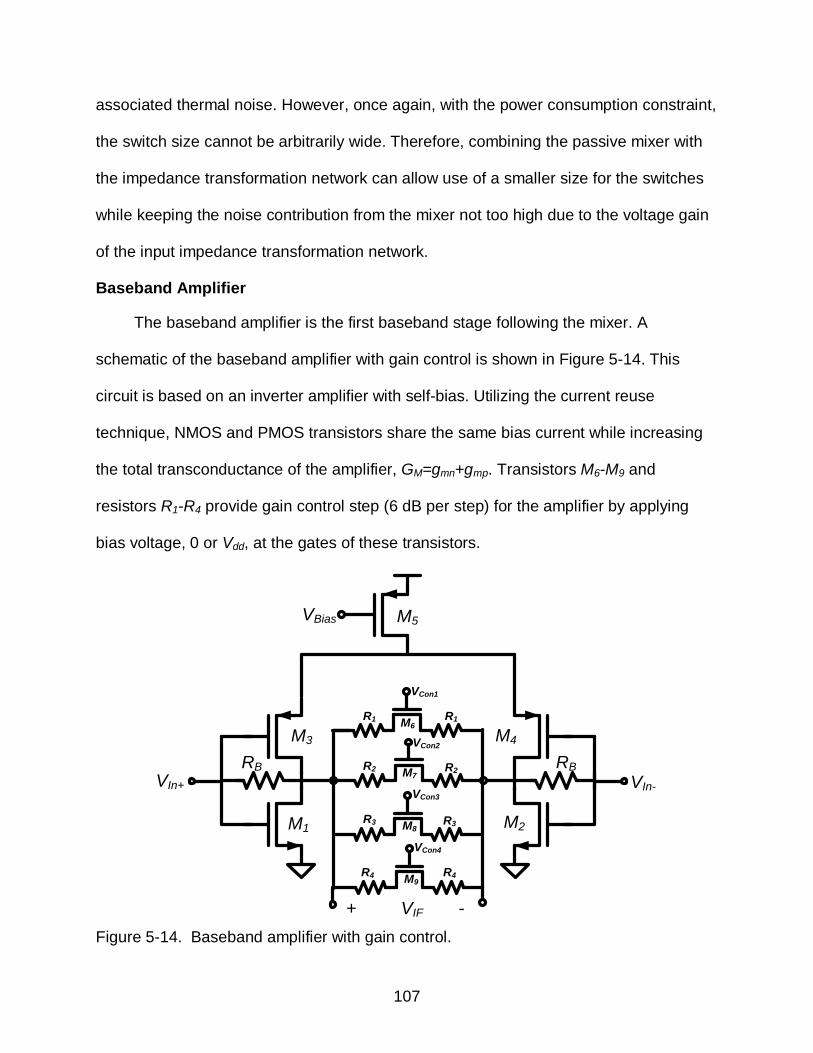
107
associated thermal noise. However, once again, with the power consumption constraint,
the switch size cannot be arbitrarily wide. Therefore, combining the passive mixer with
the impedance transformation network can allow use of a smaller size for the switches
while keeping the noise contribution from the mixer not too high due to the voltage gain
of the input impedance transformation network.
Baseband Amplifier
The baseband amplifier is the first baseband stage following the mixer. A
schematic of the baseband amplifier with gain control is shown in Figure 5-14. This
circuit is based on an inverter amplifier with self-bias. Utilizing the current reuse
technique, NMOS and PMOS transistors share the same bias current while increasing
the total transconductance of the amplifier, GM=gmn+gmp. Transistors M6-M9 and
resistors R1-R4 provide gain control step (6 dB per step) for the amplifier by applying
bias voltage, 0 or Vdd, at the gates of these transistors.
VIn+
M1
VBias
VIn-
+ VIF -
M2
M3 M4
M5
RB RB
M6
M7
M8
M9
VCon1
VCon2
VCon3
VCon4
R1 R1
R2 R2
R3 R3
R4 R4
Figure 5-14. Baseband amplifier with gain control.
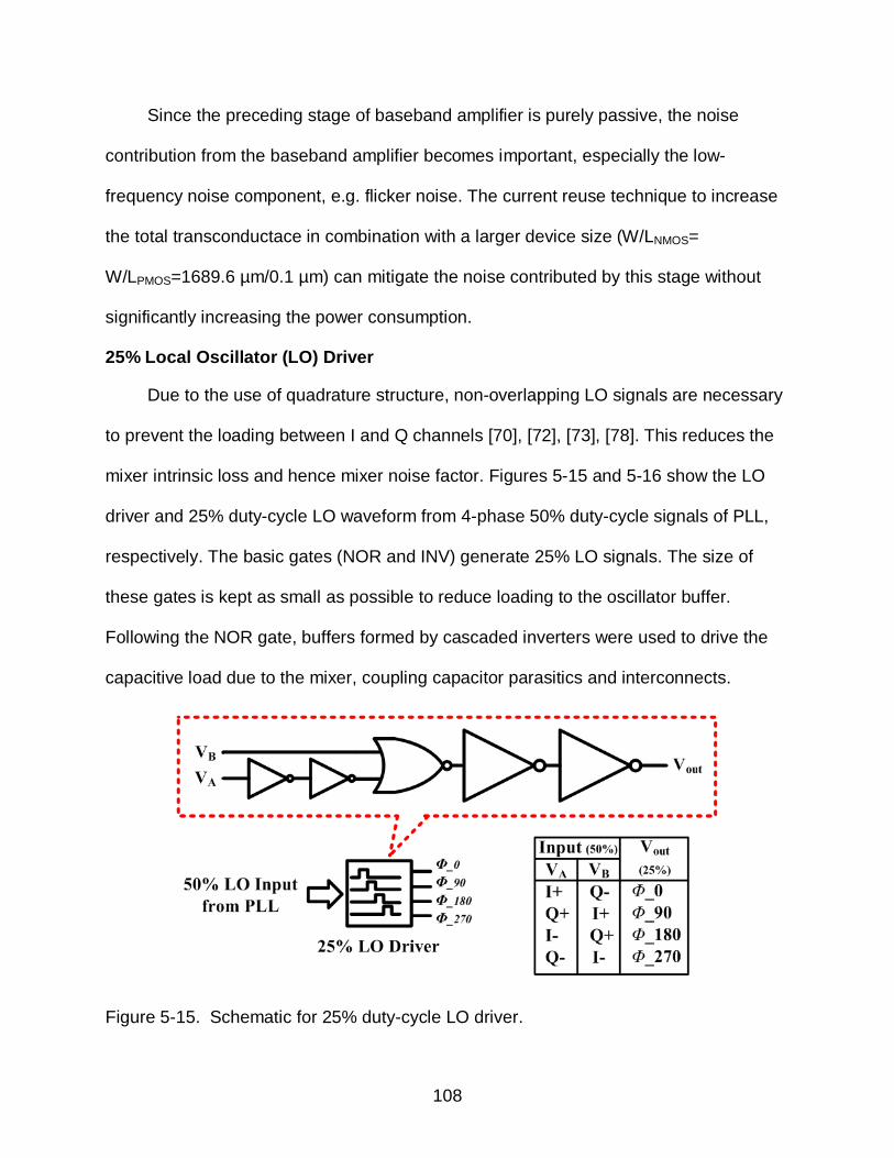
108
Since the preceding stage of baseband amplifier is purely passive, the noise
contribution from the baseband amplifier becomes important, especially the low-
frequency noise component, e.g. flicker noise. The current reuse technique to increase
the total transconductace in combination with a larger device size (W/LNMOS=
W/LPMOS=1689.6 µm/0.1 µm) can mitigate the noise contributed by this stage without
significantly increasing the power consumption.
25% Local Oscillator (LO) Driver
Due to the use of quadrature structure, non-overlapping LO signals are necessary
to prevent the loading between I and Q channels [70], [72], [73], [78]. This reduces the
mixer intrinsic loss and hence mixer noise factor. Figures 5-15 and 5-16 show the LO
driver and 25% duty-cycle LO waveform from 4-phase 50% duty-cycle signals of PLL,
respectively. The basic gates (NOR and INV) generate 25% LO signals. The size of
these gates is kept as small as possible to reduce loading to the oscillator buffer.
Following the NOR gate, buffers formed by cascaded inverters were used to drive the
capacitive load due to the mixer, coupling capacitor parasitics and interconnects.
Figure 5-15. Schematic for 25% duty-cycle LO driver.

109
I+
Q+
I-
Q-
Φ_0
Φ_90
Φ_180
Φ_270
Figure 5-16. 25% duty-cycle LO wave form.
µNode Receiver Front-End
Figure 5-17 shows the simplified schematic of the µNode receiver front-end. A
high-Q off-chip inductor (~6.2 nH, Q > 70) [79] and parasitic inductance from a PCB
trace and a bond wire are used to implement L1. The capacitors C1 and C2 are
implemented on chip by high-density metal flux capacitors [20] with capacitance of ~220
and ~340 fF, respectively. Typically, the LO driver consumes a significant portion of the
total power, thus its power consumption must be optimized. LO driver power
consumption on first order depends on its capacitive load including the loading
associated with the mixer switch transistors. Therefore, to reduce power consumption,
LO driver and mixer switch transistor width must be co-optimized. Figure 5-18 shows
simulated maximum conversion gain and spot noise figure at intermediate frequency of
1 MHz versus mixer transistor width. To achieve noise figure of less than 10 dB, the
transistor size for mixer can be small (W=1.6 µm, L=0.04 µm). The noise figure
minimum is reached when the transistor width is ~1.6-2.5 µm. The small capacitive load
associated with this transistor size in series with large coupling capacitor CLO (100 fF

110
with parasitic capacitance of ~3 fF compared to transistor gate capacitance of ~1 fF)
increases the LO amplitude at the mixer and reduces loading to the LO driver. This can
allow use of a smaller buffer with reduced power dissipation. Based on these, 1.6-µm
width is chosen for the mixer switch transistors.
Figure 5-17. Simplfied schematic of µNode receiver front-end.
This figure also shows the dependence of noise figure on the LO buffer stages.
Adding a 2-stage buffer with the 2nd stage PMOS width=5.92 µm and NMOS width=2.4
µm improves the noise figure by ~0.6 dB near the mixer transistor width of ~2 µm. The
channel length is 0.04 µm. Adding a 4-stage buffer with 4th stage PMOS width=23.68

111
µm and NMOS width=9.6 µm, degrades the noise figure because of increased noise
from the buffer.
In these simulations, the power consumption of 25% LO generation circuit without
a buffer, with a 2-stage buffer, and with a 4-stage buffer are 0.42, 0.56 and 1.4 mW,
respectively. Since, adding no buffer would increase the sensitivity of circuit to layout
and parasitic variations, a 2-stage buffer that also reduces noise figure has been
chosen. This front-end in simulation achieves 42-dB conversion gain and 8.7-dB spot
noise figure at 1-MHz offset.
Figure 5-18. Simulated conversion gain and noise figure of receiver versus the mixer transistor width.
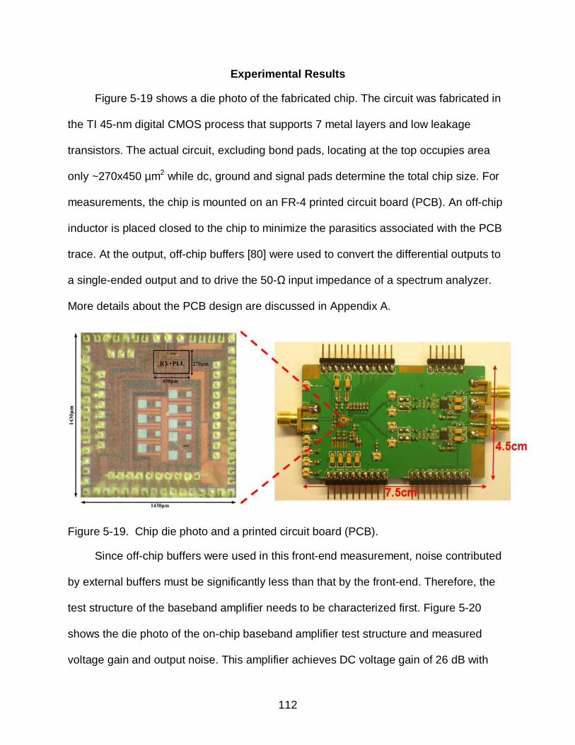
112
Experimental Results
Figure 5-19 shows a die photo of the fabricated chip. The circuit was fabricated in
the TI 45-nm digital CMOS process that supports 7 metal layers and low leakage
transistors. The actual circuit, excluding bond pads, locating at the top occupies area
only ~270x450 µm2 while dc, ground and signal pads determine the total chip size. For
measurements, the chip is mounted on an FR-4 printed circuit board (PCB). An off-chip
inductor is placed closed to the chip to minimize the parasitics associated with the PCB
trace. At the output, off-chip buffers [80] were used to convert the differential outputs to
a single-ended output and to drive the 50-Ω input impedance of a spectrum analyzer.
More details about the PCB design are discussed in Appendix A.
Figure 5-19. Chip die photo and a printed circuit board (PCB).
Since off-chip buffers were used in this front-end measurement, noise contributed
by external buffers must be significantly less than that by the front-end. Therefore, the
test structure of the baseband amplifier needs to be characterized first. Figure 5-20
shows the die photo of the on-chip baseband amplifier test structure and measured
voltage gain and output noise. This amplifier achieves DC voltage gain of 26 dB with

113
gain step of ~5 dB and 3-db bandwidth of ~2 MHz. The measured output noise voltage
is ~140 nV/√Hz at 100 kHz which agrees well with the simulated result. Compared to
the input referred noise of the external buffer which is ~12 nV/√Hz at the same
frequency [80], output noise of the on-chip baseband amplifier is much larger. So, noise
contributed by the off-chip buffer can be neglected.
Figure 5-20. Baseband amplifier test structure and its measured performance.
Figure 5-21 and 5-22 shows measurement setup and the measured PLL output,
respectively. The external signal generator provides a 50-MHz frequency reference for

114
the PLL. An on-chip inverter buffer was used to measure PLL output. The peak output
power is ~-4.7 dBm at 2.4 GHz. Measured phase noise is ~-92.8 and ~-89.3 dBc/Hz at
1 and 5 MHz frequency offset, respectively. LO leakage at RF input is ~-74.2 dBm. The
PLL provides 4-phase LO signals for the receiver front-end and measured |S11| of the
front-end is shown in Figure 5-23. The resonant frequency is tuned at ~2.34 GHz due to
the limited choices for the off-chip inductor values. However, |S11| is still <-10 dB at 2.4
GHz.
Figure 5-21. Measurement setup.

115
Figure 5-22. Measured PLL output.
Figure 5-23. Measured |S11| of the receiver front-end.

116
Figures 5-24 and 5-25 show measured voltage conversion gain and noise figure of
the front-end, respectively. The front-end achieves voltage conversion gain of ~40 dB
with 3-dB bandwidth of ~2 MHz. This bandwidth is lower than the design target of 2.5
MHz in simulation due to additional parasitic capacitance from the off-chip buffer and
PCB traces. At 1-MHz intermediate frequency, the double side band (DSB) noise figure
is ~9.2 dB and the estimated 1/f noise corner is ~250 kHz. The noise figure increases at
frequency > 4 MHz due to the gain roll-off of the off-chip buffer.
Figure 5-24. Voltage conversion gain of the receiver front-end.
Figure 5-26 is the measured second-order and third-order input intercept points
(IIP2 and IIP3, respectively) of the front-end at different IF frequencies. The spacing
between two-tone signals is chosen so that the intermodulation, IM, products fall in-
band at 30 kHz for all cases. At low IF frequency, both IIP2 and IIP3 increase as the gain
decreases [81] and flatten out or start to decrease at higher IF frequency. The decrease

117
of IIP2 at higher IF frequency is due to a gain roll-off from the baseband amplifier as well
as the mixer nonlinearity [81], [82]. At 1-MHz IF frequency, the front-end achieves IIP3
of ~-19 dBm and IIP2 of ~13 dBm. Because this front-end is focused on the integration
of the receiver front-end and PLL to achieve very low power consumption and compact
size, little effort was made to linearize the baseband and reject the interference. In
future designs, re-designing the baseband circuits and utilizing the interference filtering
can improve this linearity.
Figure 5-25. Measured noise figure of the receiver front-end.
Figure 5-27 shows the breakdown of power consumption for the receiver. The
receiver front-end including the 25% LO driver consumes power of ~1.6 mW, while the
PLL including the oscillator buffer consumes ~1.9 mW. The power consumption of the
oscillator buffer is separated from that of the PLL. Even after considerable efforts for

118
optimization, the majority of power is consumed by the PLL and LO generation circuits
(an oscillator buffer and a 25% LO driver). The supply voltage for all the circuits was 1.1
V except the 1.4V for the 25% LO driver. Table 5-1 compares the results from this work
with those of other published low power front-end designs. Even with integration of a
PLL, the design reported in this µNode front-end consumes lower power and occupies a
smaller area than several while achieving useful conversion gain and noise figure.
Figure 5-26. Measured second-order and third-order input intercept points (IIP2 and IIP3).
Figure 5-27. Power consumption summary for µNode front-end.

119
Table 5-1. Performance comparison Parameters
[70] [72] [73] [74] This work
Freq.(GHz) 2.4 2.4 2 2.4 2.4 Conv.Gain (dB) N/A 37 30 76 40 NF (dB) 5.1 6 3.1 10 9.2 1/f Corner (kHz) N/A N/A 40 N/A 250 IIP3 (dBm) -7.5 -12 -12 -13 -19 Area (mm2) 2.6 0.07 0.52 0.23 0.12 VDD(V) 0.6 1.35 1.5 1.2 1.1/1.4 Power (mW) 1.45 5.4 12 3.6 3.5 Technology 130-nm
CMOS 90-nm CMOS
130-nm CMOS
90-nm CMOS
45-nm CMOS
Topology Mixer-first LNA-first LNA-first LNA-first Mixer-first LO Source Integrated
VCO Ext. LO Drive
Ext. LO Drive
Integrated VCO
Integrated PLL
Summary
This chapter presents the low-power receiver front-end for µNodes. To lower
power consumption of analog chain of a receiver, in addition to using a matching
network formed by a high-Q off-chip inductor and non-overlapping LO driver in
combination with a passive front-end, a relaxation oscillator based PLL is utilized. The
LO driver and passive mixer switch size are co-optimized for further reduction of power
consumption. An analog receiver chain incorporating the PLL was fabricated in 45-nm
CMOS and it achieves noise figure of 9.2 dB at 1MHz intermediate frequency,
conversion gain of 40 dB while consuming 3.5 mW. The 3.5-mW peak power
consumption can be supported by approximately a dime sized CR1025 lithium cell.
Assuming 0.1% duty cycle, lifetime of more than 1 year can be supported by the battery.

120
CHAPTER 6 SUMMARY AND SUGGEST FUTURE WORK
Research Summary
Approaches for making the µNode concept practical by lowering the operating
frequency from 24 down to 2.4GHz are presented. Three major concerns for a single-
chip radio: a compact antenna, an ability to turn the system on and off without any
mechanical switch and low-power consumption for longer life time are studied in this
research work.
The feasibility of compact antennas operating at 2.4 GHz is studied through
antenna characterization for both off-chip and on-chip antennas. On-chip antennas,
despite its short length, provide reasonable input impedance for matching at 2.4 GHz
and they are less sensitive to the surrounding objects than off-chip antennas. This is a
critical factor when a small-form factor is necessary. Based on simulations, it is still
possible to form a wireless communication link at useful distances by a pair of 1-cm on-
chip antennas.
By incorporating a 5.8-GHz wireless switch into a 2.4-GHz transceiver, the single
chip radio for a µNode system can be turned on and off by using RF signals. The
wireless switch achieves useful performance while its inclusion does not significantly
degrade the performance of main transceiver. This eliminates the difficulty of
incorporating a mechanical switch into a compact radio.
A low power receiver front-end for a µNode RF subsystem is presented. The
passive structure for this front-end as well as the utilization of a relaxation-oscillator
based PLL suggests the feasibility of reducing the total power consumption and chip
area while achieving reasonable performance for the communication link. These

121
suggest the feasibility of a practical M&MTM sized µNode with wireless communication
capabilities.
Suggested Future Work
This research work presented the feasibility of realizing a practical 2.4-GHz µNode
system. Each major component, an on-chip antenna, a wireless switch and a receiver
front-end have been separately characterized. To demonstrate an M&MTM sized node,
there are still much work to be completed. The list of suggested future work includes:
Improve the Performance of On-Chip Antennas.
Higher antenna gain is desirable because it increases the communication range
and lowers the transmitted power. This benefits entire µNode system. Therefore, other
possible approaches for antenna gain improvement such as thinning the substrate [83],
etching the substrate [84] underneath the antenna and utilizing antenna loading
techniques [30], [31] need to be studied.
Improve the Performance of the Wireless Switch.
The performance of wireless switch is directly related to the power conversion
efficiency of the RF-to-DC converter. To improve its performance, other circuit
topologies as well as design techniques should be studied. A low-power active-type for
the wireless switch front-end should also be studied as another approach.
Improve the Performance of the Receiver Front-End.
The 2.4-GHz receiver front-end presented in Chapter 5 consumes low power while
achieving useful performance. However, some performance metrics such as linearity
still need to be improved. This can be done by redesigning the baseband amplifier,
incorporating filtering techniques into the front-end to suppress interferences. For the
baseband amplifier, the location of the attenuator (resistors R1 to R4 together with the

122
switch M6 to M9 shown in Figure 5-12) must be connected at the input of the amplifier
rather than at the output. By doing so, the large signal will be attenuated before
reaching the amplifier resulting in better linearity. Another approach to improve the
linearity of the amplifier is to increase the allowable signal swing at the input. This can
be done by employing wide-swing circuit topology.
Complete the Receiver Chain.
The baseband circuits for the µNode receiver need to be implemented. For
example, the variable gain amplifier (VGA) and the channel-select filter need to be
designed and integrated. Finally, the integration of wireless switch, on-chip antenna, an
RF front-end and the baseband circuits needs to be done to complete the µNode
receiver.

123
APPENDIX PRINTED CIRCUIT BOARD DESIGN
Careful design of printed circuit board (PCB) for µNode front-end is necessary
because there are no dedicated on-chip bias circuits and a high-Q off-chip inductor is
also used as a part of the matching network for this µNode front-end prototype. Figure
A-1 shows a die photograph of the front-end including bond pads. Most of the bond
pads are for supply and ground connections. To reduce parasitics associated with the
bond wires, several parallel connections especially for supply and ground were
employed. Double rows of bond pads are used to accommodate the multiple
connections as well as to keep the total chip area small. The size of the bond pad is
63x68 µm2. The gap between the 1st and 2nd rows is 72 µm which is wide enough for
wire bonding.
Figure A-1. Die micrograph of µNode front-end including bond pads.

124
Because PLL and LO driver circuits were integrated with the analog front-end,
noise from digital circuits can couple to analog parts. To reduce this, inside the chip,
analog ground was separated from digital ground. On-chip bypass capacitors (metal
oxide semiconductor (MOS) capacitors) were used and placed close to each circuit
block (2-5 pF) and every DC supply pad (10 pF). All ground connections were
connected together on the PCB and off-chip bypass capacitors (10 µF) were also used
and placed as close as possible to the chip. The minimum distance between the chip
and off-chip component is limited by the design rule provided by the wire bonding
company. Figure A-2 shows suggested bonding area for µNode front-end including the
location of nearby off-chip components, the ceramic capacitor (case 0603) and the chip
inductor (case 0402) [79]. The minimum PCB pad size for wire bonding is 127x400 µm2.
Figure A-2. Bonding area for µNode PCB.
The off-chip inductor can be placed very close to the chip area due to its small
footprint. This reduces the parasitics associated with PCB trace. To further minimize the
parasitics, the ground plane on the bottom layer underneath the off-chip inductor is left
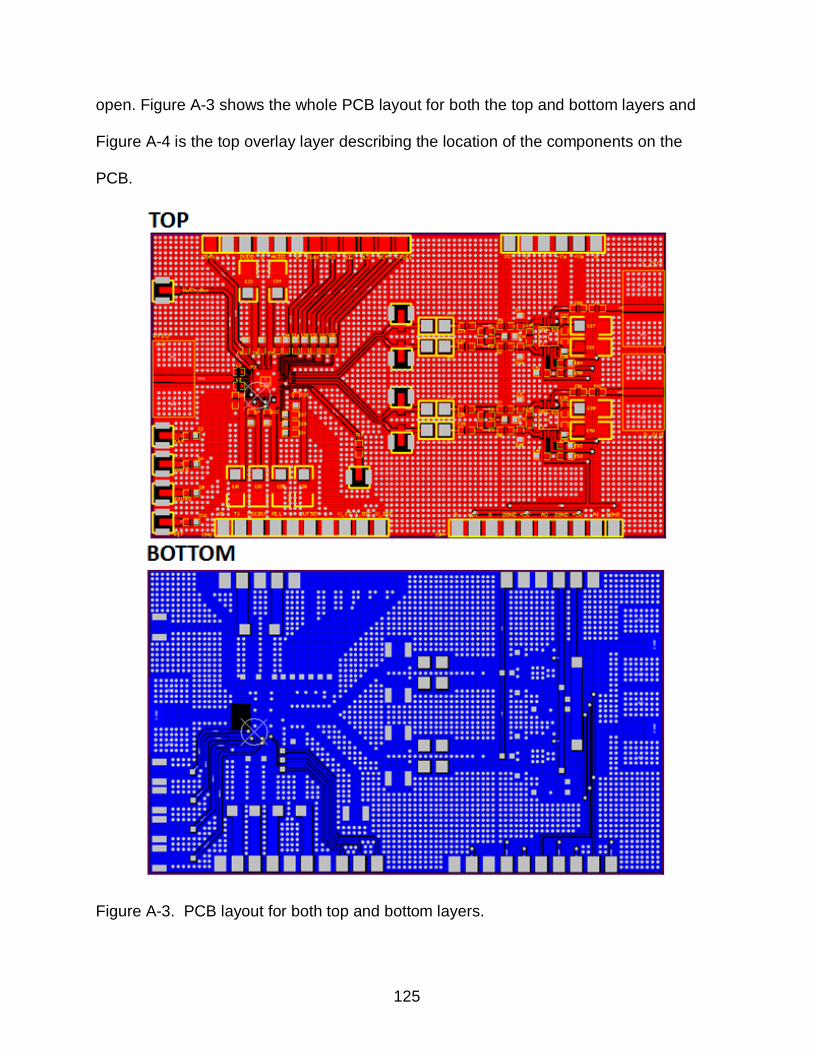
125
open. Figure A-3 shows the whole PCB layout for both the top and bottom layers and
Figure A-4 is the top overlay layer describing the location of the components on the
PCB.
Figure A-3. PCB layout for both top and bottom layers.

126
Figure A-4. Top overlay layer describing the location of the components on PCB.
Off-chip tantalum capacitors (1206) were used at the supply nodes. The off-chip
AD8253 instrument amplifiers [80] were connected at the output of µNode chip to
convert differential output into single-ended output and to drive a 50-Ω load. The supply
pins of these circuits were separated from those of the µNode circuit because the
supply voltage level is different. More details of these instrument amplifiers can be
found in [80].

127
LIST OF REFERENCES
[1] K. K. O, K. Kim, B. A. Floyd, J. Mehta, H. Yoon, C.-M. Hung, D. Bravo, T. Dickson, X. Guo, R. Li, N. Trichy, J. Caserta, W. Bomstad, J. Branch, D.-J. Yang, J. Bohorquez, L. Gao, A. Sugavanam, J.-J. Lin, J. Chen, F. Martin, and J. Brewer, “Wireless communications using integrated antennas,” in Proc. Int. Interconnect Technol. Conf., San Francisco, CA, Jun. 2003, pp. 111-113.
[2] K. K. O, J. E. Brewer, and D. Taubenheim, “RF subsystem for µNode SOC,” in 2005 Government Microcircuit Applications and Critical Technology Conf., Las Vegas, NV, Apr. 2005, Paper 9.5.
[3] K. K. O, K. Kim, B. A. Floyd, J. Mehta, H. Yoon, C.-M. Hung, D. Bravo, T. Dickson, X. Guo, R. Li, N. Trichy, J. Caserta, W. Bomstad, J. Branch, D.-J. Yang, J. Bohorquez, E. Soek, L. Gao, A. Sugavanam, J.-J. Lin, J. Chen, and J. Brewer “On-chip antennas in silicon integrated circuits and their applications,” IEEE Trans. on Electron Devices, vol. 52, no. 7, pp. 1312-1323, Jul. 2005.
[4] C. Cao, A 24-GHz Fully-Integrated CMOS Transmitter with On-chip Antenna, PhD Dissertation, University of Florida, Gainesville, FL, 2006.
[5] C. Cao, Y. Ding, X. Yang, J.-J. Lin, A. K. Verma, J. Lin, F. Martin, and K. K. O, “A 24-GHz transmitter with an on-chip antenna in 130-nm CMOS,” in Symp. VLSI Circuits Dig. Tech. Papers, Jun. 2006, pp. 184-185.
[6] C. Cao, Y. Ding, X. Yang, J.-J. Lin, H.-T. Wu, A. K. Verma, J. Lin, F. Martin, and K. K. O, “A 24-GHz transmitter with on-chip dipole antenna in 0.13-µm CMOS,” IEEE J. of Solid State Circuits, vol. 43, no. 6, pp. 1394-1402, June, 2008.
[7] J.-J. Lin, On-chip Antennas for Short-Range Wireless Communications, PhD Dissertation, University of Florida, Gainesville, FL, 2007.
[8] J.-J. Lin, H.-T. Wu, Y. Su, L. Gao, A. Sugavanam, J. E. Brewer, and K. K. O, “Communication using antennas fabricated in silicon integrated circuits,” IEEE J. of Solid-State Circuits, vol. 42, no. 8, pp. 1678-1687, August 2007.
[9] K. K. O et al., “Progress toward a single chip radio in CMOS,” in 2008 IEEE Circuits and Systems Workshop: System-on-Chip-Design, Applications, Integration, and Software, Dallas, TX, 2008, pp.1-7.
[10] Y. Su, Fully Integrated CMOS Receiver for A 24-GHz Single Chip Radio, PhD Dissertation, University of Florida, Gainesville, FL, 2009.
[11] Y. Su, J.-J. Lin, and K. K. O, “A 20-GHz CMOS RF down-converter with an on-chip antenna,” in 2005 IEEE ISSCC Dig. Tech. Papers, San Francisco, CA, Feb 2005, pp. 270-271.
128
[12] K. K. O, J. E. Brewer, J.-J. Lin, H.-T. Wu, S. Hwang, “Single chip radio transceiver power reduction,” in 2008 Government Microcircuit Applications and Critical Technology Conf., Las Vegas, NV, Apr. 2008, Invited Paper 6.1.
[13] Y. Ding, CMOS Synthesizers for 24-GHz Radios, PhD Dissertation, University of Florida, Gainesville, FL, 2007.
[14] Y. Ding and K. K. O, “A 21-GHz 8-modulus prescale and a 20-GHz phase locked loop fabricated in 130-nm CMOS,” IEEE J. of Solid-State Circuits, vol. 42, no. 6, pp. 1240-1249, June, 2007.
[15] Y. Ding, Y. Su, C. Cao, J.-J. Lin, H.-T. Wu, M. Hwang, R. Fox, J.E. Brewer, and K.K.O, “RF transceiver and wireless calibration of on-chip frequency reference for a true single chip radio,” in Proc.2008 IEEE Symp. VLSI Circuits, Honolulu, HI, Jun. 2008, pp. 116-117.
[16] K. Finkenzeller, RFID Handbook – Fundamentals and Applications in Contactless Smart Cards and Identification, 2nd Edition, John Wiley & Sons, 2003.
[17] IEEE Standards Association [Online]. Available: http://standards.ieee.org
[18] H. T. Friis, “Noise figures of radio receivers,” Proc. of IRE, vol. 32, no. 7, pp. 419-422, Jul. 1944.
[19] B. Razavi, RF Microelectrinics, Prentice Hall 1998.
[20] T. H. Lee, The Design of CMOS Radio-Frequency Integrated Circuits, 2nd Edition, Cambridge University Press, 2003.
[21] J. E. Brewer, Integrated Micronode Research Program Review for DARPA, Nov. 2008.
[22] J. D. Kraus and R. J. Marhefka, Antennas for All Applications, 3rd Edition, McGraw Hill, 2003.
[23] C. A. Balanis, Antenna Theory, 2nd Edition, John Wiley & Sons, New York, 1997.
[24] U. Karthaus and M. Fischer, “Fully integrated passive UHF RFID transponder IC with 16.7 µW minimum RF input power,” IEEE J. Solid-State Circuits, vol. 38, no.10, pp.1602-1608, Oct. 2003.
[25] A. Ricci, M. Grisanti, I.D. Munari, and P.Ciampolini, “Improved pervasive sensing with RFID: An ultra-low power baseband processor for UHF tags,” IEEE Trans. Very Large Scale Integr. (VLSI) Syst., vol.17, no. 12, pp. 1719-1729, Dec 2009.
[26] Federal Communications Commission (FCC) [Online]. Available: http://transition.fcc.gov

129
[27] H. Nakano, H. Tagami, A. Yoshizawa and J.Yamauchi, “Shortening ratios of modified dipole antennas,” IEEE Trans. on Antennas and Propag., vol.32, Issue 4 pp.385-386, April 1984.
[28] C. Zhou and H. Y. David Yang, “The design of miniaturized printed wire antennas using double-layer periodic metallization,” IEEE Antennas and Wireless Propagation Letters, vol.6, pp.11-14, 2007.
[29] W.-T. Liu and S.-T. Fang, “A planar compact CPW-FED antenna,” in Proc. APMC2001, Taiwan, 2001, pp.934-937.
[30] M. Lee, B. A. Kramer, C.-C. Chen and J. L. Volakis, “Distributed lumped loads and lossy transmission line model for wideband spiral antenna miniaturization and characterization,” IEEE Trans. on Antennas and Propag., vol.55, No.10, October 2007.
[31] B. A. Kramer, M. Lee, C.-C. Chen and J. L. Volakis, “Miniature UWB antenna with embedded inductive loading,” 2006 IEEE International Workshop on Antenna Technology: Small Antennas and Novel Metamaterials, pp.289-292, Mar 2006.
[32] M. M. Weiner, Monopole Elements on Circular Ground Planes, Artech House, 1987.
[33] R. Webster, “20-70 MC monopole antennas on ground-based vehicles,” IEEE Trans. on Antennas and Propag., vol. 5, Issue 4, pp. 363-368, Oct1957.
[34] H. Schuman, T. Baldwin, “Monopole antennas over lossy ground,” IEEE AP-S Intl. Symp. Dig. Tech. Papers, vol. 18, pp. 444-447, Jun 1980.
[35] H. J. Delgado, J. T. Williams, S. A. Long, “Substraction of edge-diffracted fields in antenna radiation patterns for simulation of infinite ground plane,” IEEE Electron. Lett., vol. 25, Issue 11, pp.694-696, 25 May 1989.
[36] Y.-M. Yu, Y.-M. Tang, and W. Wu, “Effect of a finite ground plane on Peano fractal loaded monopole antenna,” Microw. Opt. Technol. Lett., vol. 49, Issue 12, pp.3087-3090, Sep 2007.
[37] Y. Chung, J. Sun, S. Wang, S. Huang and C. Chiang, “Compact chip antenna application in GPS by LTCC processing,” Microw. Opt. Technol. Lett., vol. 51, Issue 4, pp.1017-1019, Feb 2009.
[38] Antenna Factor INC., Ultra Compact Chip Antenna Data Guide [Online]. Available: www.antennafactor.com.
[39] Y. D. Kim, H.-Y. Kim and H. M. Lee, “Dual-band LTCC chip antenna design using stacked meander patch for mobile handsets,” Microw. Opt. Technol. Lett., vol. 45, Issue 4, pp. 271-273, Apr 2005.
130
[40] AN3216, Multilayer Chip Antenna, Jan 2008 [Online]. Available:, www.rainsun.com.
[41] Performing Van Der Pauw Resistivity Measurements, Application Note 1076-304, Rev. A0, Mar 2007 [Online]. Available: www.qdusa.com.
[42] K. Kim, Design and Characterization of RF Components for Inter- and Intra-Chip Wireless Communication, PhD Dissertation, University of Florida, Gainesville, FL, 2000.
[43] S.H. Zainud-Deen, K. H. Awadalla, A. I. Bahnacy and H. A. Sharshar, “Performance analysis of zigzag antenna for portable radio equipment,” IEEE Antennas and Propagation Society International Symposium, vol.1, pp. 442-447, Jul 1997.
[44] H. Nakano, H. Tagami, J. Yamauchi, “Numerical analysis of an axial-mode zigzag antenna,” IEEE Electron. Lett., vol. 21, Issue 14, pp. 606-608, Jul 1985.
[45] J.-J. Lin, H.-T. Wu and K. K. O, “Compact on-chip monopole antennas on 20-Ω-cm silicon substrates for operation in the 5.8-GHz ISM band,” IEEE Int. Electron Devices Meeting Dig. Tech. Papers, pp. 947-950, Dec. 5, 2005.
[46] A. R. Djordjević, A. G. Zajić, and M. M. Ilić, “Enhancing the gain of helical antennas by shaping the ground conductor,” IEEE. Antennas and Wireless Propag. Lett., vol.5, pp. 138-140, Dec. 2006.
[47] Compact Integrated Antennas, Application Note Rev. 1.4, Jul 2006 [Online]. Available: www.freescale.com.
[48] L. Desclos, “Advances in high-performance ceramic antennas for small-form-factor, multi-technology devices,” Microwave Journal, Dec 2, 2008.
[49] N. Pletcher, S. Gambini, J. Rabaey, “A 65µW, 1.9 GHz RF to digital baseband wakeup receiver for wireless sensor nodes,” in Proc. IEEE Custom Integrated Circuits Conf., CICC’07, 2007, pp.539-542.
[50] G. Lin and S. John, Radio-triggered wake-up for wireless sensor networks, Charlottesville, VA:Dept. Comput. Sci., Univ. Virginia.
[51] J. Ansari, D. Pankin, and P. Mahonen, “Radio-triggered wake-ups with addressing capabilities for extremely low power sensor network applications,” in IEEE 91th Int. Symp. Personal, Indoor and Mobile Radio Communications, PMIRC 2008, Sept. 15-18, 2008, pp.1-5.
[52] Y.-F. Lin, C.-H Lin, H.-M. Chen and P.S. Hall, “A miniature dielectric loaded monopole antenna for 2.4/5 GHz WLAN applications,” IEEE Microw. Wireless Compon. Lett., vol. 16, no. 11, pp.591-593, Nov. 2006.

131
[53] AN1003 Multilayer Chip Antenna, June 2006 [Online]. Available: www.rainsun.com
[54] T.-H. Kim and D.-C. Park, “Compact dual-band antenna with double L-slits for WLAN operations,” IEEE Antennas Wireless Propag. Lett., vol. 4, pp. 249-252, 2005.
[55] L.-C. Chou and K.-L. Wond, “Uni-planar dual-band monopole antenna for 2.4/5 GHz WLAN operation in the laptop computer,” IEEE Trans. Antennas Propag., vol. 55, no. 12, Dec. 2007.
[56] J.P. Curty, N. Joehl, C. Dehollain and M.J. Declercq, “Remotely powered addressable UHF RFID integrated system,” IEEE J. Solid-State Circuits, vol. 40, no.11, pp.2193-2202, Nov. 2005.
[57] J.P. Curty, N. Joehl, F Krummenacher. C. Dehollain and M.J. Declercq, “A model for µ-power rectifier analysis and design,” IEEE Trans. on Circuits and Systems, vol. 52, no.12, pp.2771-2779, Dec. 2005.
[58] G. De Vita and G. Iannaccone, “Design criteria for the RF section of UHF and microwave passive RFID transponders,” IEEE Trans. on Microw. Theory and Tech., vol. 53, Issue 9, pp.2978-2990, Sept. 2005.
[59] T.Umeda, H. Yoshida, S.Sekine, Y.Fujita, T.Suzuki, and S.Otaka, “A 950-MHz rectifier circuit for sensor network tags with 10-m distance,” IEEE J. Solid-State Circuits, vol 41, no.1, pp.35-41, Jan. 2006.
[60] J. O. McSpadden, L. Fan, and K. Cheng, “Design and experiments of a high-conversion-efficiency 5.8-GHz rectenna,” IEEE Trans. on Microw. Theory and Tech., vol. 46, No.12, pp.2053-2060, Dec. 1998.
[61] H. Nakamoto et al., “A passive UHF RFID tag LSI with 36.6% efficiency CMOS-only rectifier and current-mode demodulator in 0.35um FERAM technology,” in IEEE Int. Solid-State Circuits Conf. (ISSCC) Dig. Tech. Papers, Feb2006, pp.310-311.
[62] F.-J. Huang and K. K. O, “Metal-oxide semiconductor field effect transistors using Schottky barrier drains (SBDR),” IEEE Electron. Letters, vol. 33, no. 15, pp. 1341-1342, July, 1997.
[63] S. Sankaran and K. K. O, “A ultra-wideband amplitude modulation (AM) detector using Schottky barrier diodes fabricated in foundry CMOS Technology,” IEEE J. Solid-State Circuits, vol.42, no.5, pp. 1058-1064, May 2007.
[64] S. Sankaran, Receivers Using Schottky Barrier Diodes in CMOS, PhD Dissertation, University of Florida, Gainesville, FL, 2008.

132
[65] D. Johns and K. Martin, Analog Integrated Circuit Design, John Wiley & Sons, Inc., 1996.
[66] R. J. Baker, CMOS Circuit Design Layout and Simulation. New York: IEEE Press, 2007.
[67] Z. Li and K.K.O, “15-GHz fully integrated nMOS switches in a 0.13-µm CMOS process,” IEEE J. Solid-State Circuits, vol. 40, no.11, pp.2323-2328, Nov 2005.
[68] T. Le, K. Mayaram, and T. Fiez, “Efficient far-field radio frequency energy harvesting for passively powered sensor networks,” IEEE J. Solid-State Circuits, vol. 43, no.5, pp.1287-1302, May. 2008.
[69] B. Razavi, Fundamentals of Microelectronics, John Wiley & Sons, Inc., 2006.
[70] B.W. Cook, A. Berny, A. Molnar, S. Lanzisera and K.S.J. Pister, “Low power 2.4GHz transceiver with passive RX front-end and 400mV supply,” IEEE J. Solid-State Circuits, vol. 41, no.12, pp.2757-2766, Dec 2006.
[71] S. Zhou and M.F. Chang, “A CMOS passive mixer with low flickner noise for low-power direct conversion receiver,” IEEE J. Solid-State Circuits, vol. 40, no.5, pp.1084-1093, May 2005.
[72] M. Camus, B. Butaye, L. Garcia, M. Sié, B.Pellat, and T. Parra, “A 5.4 mW/0.07 mm2 2.4GHz front-end receiver in 90 nm CMOS for IEEE 802.15.4 WPAN standard,” IEEE J. Solid-State Circuits, vol. 43, no. 6, pp.1372-1383, Jun. 2008.
[73] Y. Feng, G. Takemura, S. Kawaguchi, and P. Kinget, “Design of a high performance 2-GHz direct-conversion front-end with a sign-ended RF input in 0.13 µm CMOS,” IEEE J. Solid-State Circuits, vol. 44, no. 5, pp.1380-1390, May 2009.
[74] M. Tedeschi, A. Liscidini, and R. Castello, “Low-power quadrature receiver for ZigBee (IEEE 802.15.4) applications,” IEEE J. Solid-State Circuits, vol. 45, no. 9, pp.1710-1719, Sep. 2010.
[75] N. M. Pletcher, S. Gambini, and J. Rabaey, “A 52 µW wake-up receiver with -72 dBm sensitivity using an uncertain-IF architecture,” IEEE J. Solid-State Circuits, vol. 44, no. 1, pp.269-280, Jan. 2009.
[76] Shahani, D. Sharffer and T. Lee, “A 12-mW wide dynamic range CMOS front-end for a portable GPS receiver,” IEEE J. Solid-State Circuits, vol. 32, no.12, pp.2061-2070, Dec. 1997.
[77] C.D. Hull and R.G. Meyer, “A systematic approach to the analysis of noise in mixers,” IEEE Trans. on Circuits and Systems, vol. 40, no.12, pp.909-919, Dec. 1993.

133
[78] M.C.M Soer, et al, “A 0.2-to-2.0GHz 65nm CMOS receiver without LNA achieving >11dBm IIP3 and <6.5dB NF,” IEEE Int. Solid-State Circuits Conf. Dig. Tech. Papers, Feb. 2009, pp.222-224.
[79] Ceramic Chip Inductors [Online]. Available: www.coilcraft.com.
[80] AD8253, Programmable Gain Instrumentation Amplifier [Online]. Available: www.analog.com.
[81] I. Elahi, K. Muhummad, and P. T. Balsara, “IIP2 and DC offsets in the presence of leakage at LO frequency,” IEEE Trans. Circuits Syst. II, Analog Digit. Signal Process., vol. 53, no. 8, pp. 647-651, Aug. 2006.
[82] N. Poobuapheun, W.-H. Chen, Z. Boos, and A. M. Niknejad, “A 1.5-V 0.7-2.5-GHz CMOS quadrature demodulator for multiband direct-conversion receivers,” IEEE J. Solid-State Circuits, vol. 42, no.8, pp.1669-1677, Aug. 2007.
[83] K. Kimoto, N. Sasaki, S. Kubota, W. Moriyama and T. Kikkawa, “High-gain on-chip antennas for LSI intra-/inter-chip wireless interconnection,” European Conference on Antennas and Propagation, pp.278-282, Mar. 2009.
[84] J. Gemio, J. Parron, P. De Paco, J. Sacristan, and A. Baldi, “Improving silicon integrated antennas by substrate micromachining: A study of etching patterns,” Progress In Electromagnetics Research, vol. 117, pp.365-378, 2011.

134
BIOGRAPHICAL SKETCH
Wuttichai Lerdsitsomboon received the Bachelor of Engineering in electrical
engineering from Chulalongkorn University, Bangkok, Thailand, in 2003. In 2005, he
went to United States to continue his graduate study. He received his Master of Science
in electrical and computer engineering from the University of Florida, Gainesville, in
2006. Since then, he has been a Ph.D candidate in the same department, and with the
Silicon Microwave Integrated Circuits and Systems (SIMICs) Research Group. His
research interests are low power radio frequency integrated circuits (RFICs), on-chip
antennas and analog circuit design in complementary metal oxide semiconductor
(CMOS) technology.