low-voltage switched-opamp circuits - university …kphang/papers/2002/ryuen_swopamp.pdfuniversity...
TRANSCRIPT

University of Toronto Department of Electrical and Computer Engineering
Low-Voltage Switched-OpAmp Circuits
Analog Circuit Design I ECE1352F
Term Paper
University of Toronto Electronics Group Toronto, Ontario
Prepared By: Name: Ricky Yuen (ryuen@eecg)
Student ID: 971339500 Date: November 15, 2002

Table of Contents Table of Contents ..................................................................................................... ii
List of Figures ......................................................................................................... iii
1.0 Abstract..........................................................................................................1
2.0 Introduction.................................................................................................. 2
3.0 The Basics of Switched Capacitor Circuit..................................................... 3
3.1 Capacitors ........................................................................................................... 3
3.2 Operational Amplifiers ....................................................................................... 4
3.3 MOSFET Switches ............................................................................................. 4
4.0 Problems faced by SC Circuit with Low Supply Voltage.............................. 6
5.0 Possible Solutions to SC Circuits with Low Supply Voltage ........................ 9
6.0 The Switched OpAmp Techniques ............................................................... 9
7.0 Modern State of the Art SO Circuits............................................................12
8.0 Conclusions and Future Directions............................................................. 15
9.0 References....................................................................................................16
ii

List of Figures Figure 3-1 Switched capacitor circuit used in an integrator. .................................. 3
Figure 3-2 Cross sectional view of poly-poly capacitor........................................... 4
Figure 3-3 pMOS and nMOS implemented pass transistor switches......................5
Figure 3-4 Conductance of CMOS a typical switch with VDD = 5V. ........................ 6
Figure 4-1 Conductance of CMOS a typical switch with VDD = 1V. ..........................7
Figure 4-2 Simplified version of 2-stage OpAmp. .................................................. 8
Figure 6-1 First proposed switched-OpAmp circuit...............................................10
Figure 6-2 A typical low-Q biquad filter realized with SC circuit. ......................... 11
Figure 6-3 The low-Q biquad filter realized with SO circuit..................................12
Figure 6-4 Table illustrating switched OpAmp circuit in action. ..........................12
Figure 7-1 State of the art switched OpAmp circuit. ..............................................13
Figure 7-2 CMFB circuit for new proposed switched OpAmp circuit....................14
Figure 7-3 CMFB when switched OpAmp is OFF. ................................................. 15
Figure 7-4 CMFB when switched OpAmp is ON.................................................... 15
iii

1.0 Abstract With the demand of low power applications, running circuits with reduced supply
voltage can be of great advantage. Switched capacitor circuit is well known for
their high linearity even with voltage supply variation since the capacitor value is
only dependent on the process. However, when running the switched capacitor
circuit with a reduced voltage supply, problems with the switches arise as they
cease to function within a portion of the operating voltage range. A technique
called switched OpAmp is proposed as a solution. The problematic switches are
replaced with OpAmps that are capable of switching ON and OFF to mimic the
operation of the switches. This method is proven to be feasible along with some
power savings since the OpAmp is in operation for only half of the clock cycle.
New research proposed a fully differential version of the switched OpAmp along
with a fast common mode feedback circuit that reduce the “turn on” time of the
OpAmp such that the sampling frequency can be greatly increased. This
improved switched OpAmp circuit is capable of running at 1.0V in 0.35um
process. Future research is targeted for further reducing the “turn on” time of the
switched OpAmp by using new common mode feedback circuit. As a result,
faster sampling frequency can be achieved.
1

2.0 Introduction In the last decade, one of the aims of the electronic research is towards low power
applications. With the need of portable devices in the market, an important
specification is the available battery life of the equipment. For example, business
users cannot tolerate to have their cell phones charged after a few conversations.
Thus, the transceiver integrated circuit (IC), which usually is the main power
consumer, should be designed such that it consumes as little power as possible
when it is in operation.
From the classical analysis of complementary metal oxide semiconductor
(CMOS) [1], feasible ways to reduce the power consumption include reducing
voltage swing and voltage supply of the circuit. There are two ways to reduce the
voltage swing of the signals. First is to create special circuitry to generate the
reduced signal swing with the regular power supply, which adds complexity.
Second is to run the circuit under a lowered voltage supply and in effect, reduced
the voltage swing of the signal. The second option seems to be very attractive
because power consumption decreases with the voltage supply in a square law
relationship.
With technology scaling, power supply voltage has been scaled down from 3.3V
(0.35um CMOS) to currently 1.2V (0.13um CMOS). This definitely introduced a
huge amount of power saving along with performance enhancement. However, it
is even more advantageous if the device can operate with a supply voltage that is
even lower than the normal specified level.
Switched capacitor (SC) circuit has been a popular choice in circuit design. Not
to mention that they can convert the signal into the digital domain, they also
provide high linearity that is essential to modern circuitry [1]. This paper will
2
focus on the problems faced with switched capacitor circuits designed to run on a
reduced voltage supply along with the proposed solutions.
3.0 The Basics of Switched Capacitor Circuit
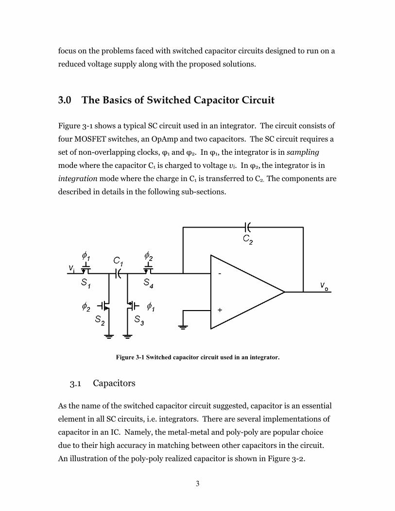
Figure 3-1 shows a typical SC circuit used in an integrator. The circuit consists of
four MOSFET switches, an OpAmp and two capacitors. The SC circuit requires a
set of non-overlapping clocks, φ1 and φ2. In φ1, the integrator is in sampling
mode where the capacitor C1 is charged to voltage vi. In φ2, the integrator is in
integration mode where the charge in C1 is transferred to C2. The components are
described in details in the following sub-sections.
Figure 3-1 Switched capacitor circuit used in an integrator.
3.1 Capacitors
As the name of the switched capacitor circuit suggested, capacitor is an essential
element in all SC circuits, i.e. integrators. There are several implementations of
capacitor in an IC. Namely, the metal-metal and poly-poly are popular choice
due to their high accuracy in matching between other capacitors in the circuit.
An illustration of the poly-poly realized capacitor is shown in Figure 3-2.
3

Figure 3-2 Cross sectional view of poly-poly capacitor.
3.2 Operational Amplifiers
Operational Amplifier (OpAmp) is the main driving component in the switched
capacitor circuit. Thus, its performances, i.e. DC gain, unity gain frequency, slew
rate and phase margin, directly affect the characteristic of the SC circuit. Modern
popular OpAmp topology includes the folded cascode and two-stage Miller
compensated OpAmp. They are suitable for working in today’s low voltage
supply environment due to the fact that they have less cascoded devices; thus,
result in a larger signal swing.
3.3 MOSFET Switches
MOSFET switch is implemented by either the choice of pMOS or nMOS, or both.
Single MOSFET switch implemented by either pMOS or nMOS cannot pass logic
‘0’ or logic ‘1’ respectively. Figure 3-3 illustrates the reasoning.
4

Figure 3-3 pMOS and nMOS implemented pass transistor switches.
To illustrate the idea, only nMOS version will be considered; however, the same
reason can be applied for pMOS switch. For conduction, the nMOS must satisfy
the following relationship, 0>− THGS V
DD
V . The source of an nMOS is usually the
side with the lower voltage and it is the right side of the nMOS in Figure 3-3.
With the gate of the nMOS connected to VDD, the maximum voltage that the
capacitor can charge up is equal to V THV− before the nMOS goes into cut-off
region. The same reasoning applies to the pMOS counterpart, which only passes
voltage down to V . As a result, CMOS switch is usually used since they allow
passing of full logic level, from VSS to VDD. Figure 3-4 shows the range of voltages
pass by the nMOS and pMOS in a CMOS switch. From V to 1.2V, only the
nMOS is in conduction and pMOS is in cutoff. From 3.7V to V , only the pMOS
is in conduction. Between 1.2V and 3.7V, both device is ON and the conductance
adds up.
TH
SS
DD
5

Figure 3-4 Conductance of CMOS a typical switch with VDD = 5V.
4.0 Problems faced by SC Circuit with Low Supply Voltage
With the supply voltage lowered, i.e. 1.0V, capacitor faced no problem since it is
only technology and fabrication dependent [2]. Nevertheless, OpAmp does have
some impact when running with a reduced supply voltage. Due to the fact that
transistors in an OpAmp are required to operate in the saturation region,
, cascoding transistors to realize a higher equivalent impedance
becomes more difficult because they reduce the available voltage swing. It is
necessary to have the largest voltage swing to maintain a certain amount of noise
margin when working with a reduced voltage supply. As a result, telescopic
cascoded OpAmp is impractical when working with low voltage applications. A
feasible OpAmp topology is the two-stage Miller compensated OpAmp. They
provided the high DC gain by cascading a transconductance (Gm) stage with an
output stage (providing the large swing) together.
THGSDS VVV −>
The CMOS switch also has problem when working with a reduced voltage supply.
For example, in the 0.35um process, the threshold voltage, V , of pMOS and
nMOS is equal to 0.736V and 0.546V respectively [1]. When using a low voltage
TH
6

supply, V , the pMOS can pass 0.736V to V and the nMOS can pass V
to 0.454V as explained previously. This is illustrated in Figure 4-1.
VDD 0.1= DD SS
Figure 4-1 Conductance of CMOS a typical switch with VDD = 1V.
Clearly, there is a region, 0.454V to 0.736V, where both the pMOS and the nMOS
are not conductive, which creates high non-linearity in the SC circuit.
From the above discussion, it is obvious that both the OpAmp and the MOSFET
switches have problems when working with a reduced voltage supply. To find out
the limiting factor, the simplified two-stage OpAmp circuit is shown in Figure
4-2.
7

Figure 4-2 Simplified version of 2-stage OpAmp.
From Figure 4-2, it is apparent that the minimum VDD to keep the OpAmp
functional (i.e. all transistors in saturation) is equal to
, given that satsat DSpswingDSnDDopamp VVVV ++=
min THswing V
V>
2, which is dominated by the
output stage of the OpAmp [3].
For the MOSFET switch and assuming only nMOS is used, the gate voltage (clock
signal) has to be at least V higher than the largest voltage that it wants to pass.
With the configuration shown in Figure 4-2, the highest voltage that the nMOS
switch needs to pass is the highest output voltage swing, V
TH
swingDSn Vsat+ , so the gate
voltage applied must be at least VminDDswitchTH VV
min swingDSnGswitch VVsat
=++= .
Therefore, the above analysis concluded that the switch is the limiting factor that
dictates the minimum voltage supply since V . minDDopampminDDswitch V>
8

5.0 Possible Solutions to SC Circuits with Low Supply Voltage
Previously proposed solutions to the above problem included (1) the use of a low
threshold device [4] and (2) the use of voltage multiplier to generate higher gate
voltage only for the switch [5].
Solution (1) involves higher cost because it requires a special process. That cost
will be pass on to the consumer and it will affect the marketability of the product.
Also, a lowered threshold voltage, V , will result in a higher sub-threshold
leakage current, which decreased the power saved by using a reduced voltage
supply and caused charge leakage problem in the capacitor.
TH
Solution (2) is a popular choice; however, it requires extra circuitry on chip to do
the voltage multiplying. The voltage multiplying circuit increases the power
consumption, chip area and complexity. Moreover, modern sub-micron
technology has a much thinner gate oxide. If a higher than specified gate voltage
is applied, it will cause long-term reliability problem.
6.0 The Switched OpAmp Techniques
Another solution to the switch working with reduced voltage supply is the
switched OpAmp technique. Switched OpAmp (SO) is introduced by Crols and
Steyaert in 1994. The basic idea of the switched OpAmp is to replace the
MOSFET switch with a special OpAmp that has an ON and OFF states.
Carefully examining Figure 3-1 indicated that not all the MOSFET switches have
problem with a low voltage supply. Switches 2, 3 and 4 have their source node
always connected to VSS or a virtual ground; therefore, the problem is alleviated
by using an nMOS, which can pass logic ‘0’ completely. Switch 1 is connected to
the output node of the previous stage and the capacitor. Its purpose is to let C1
9

charges to the voltage of the previous output node. As a result, switch 1 is the
only switch in the SC circuit that has the problem discussed above.
It is not possible to remove that switch because it will short the output of the
OpAmp to VSS in the φ2 phase. However, since in φ2, the previous stage is in the
sampling phase, the OpAmp can be switched off or turned into high impedance.
This is equivalent to shutting off switch 1 in the signal path. Since the
problematic switch is removed, the minimum power supply voltage is dictated by
the OpAmp and is equal to Vsatsat DSpswingDSnDDopamp VVV ++=
min if rail-to-rail voltage
swing is desired [3].
Figure 6-1 shows the schematic of a switched OpAmp. This is the commonly
known 2-stage Miller compensated OpAmp with two more transistors added, M9
and M10. They are driven by the same phase clock and served as the switches
used to switch the OpAmp into a high impedance state.
Figure 6-1 First proposed switched-OpAmp circuit.
10

When the clock is logic high, the OpAmp is in normal operation; M9 is ON and
M10 is OFF. When the clock is logic low, the OpAmp is in high impedance state.
M9 is OFF and prevents the discharge of the sampling capacitor in the following
stage. Also M10 is ON such that the voltage VDD will be applied to all the current
mirrors and shuts them off. As a result, the OpAmp is completely shut off when
the integrator is in sampling phase.
To illustrate the operation of the SO circuit, the following example shows a
problematic switch in a low-Q biquad filter is replaced with the SO circuit.
Figure 6-2 A typical low-Q biquad filter realized with SC circuit.
In Figure 6-2, the highlighted switch is replaced by the switched OpAmp
integrator in Figure 6-3. An extra switched OpAmp in the SO circuit is needed
because the first OpAmp in the SC circuit has to drive capacitor C3 at φ2. By
shutting off SO1 (equivalent to first OpAmp in the SC circuit) at φ2 in the SO
circuit, it can no longer drive C3. Thus, a non-inverting delay (integrator 2) is put
in. Although this increased the number of SO, the power dissipation is decreased
by 0.75 because all three SO are in operation for half of the clock cycle [3]. Figure
6-4 detailed the operations of all the integrators in the low-Q biquad circuit.
11

Figure 6-3 The low-Q biquad filter realized with SO circuit.
Time Integrator 1 Integrator 2 Integrator 3
φ1 Integrate C2 Sample C3 Discharge C5
φ2 Sample C1 Integrate C4 Integrate C6/7
Figure 6-4 Table illustrating switched OpAmp circuit in action.
During the time that the OpAmp is recovering from OFF to ON state, transistor
M8 is used to charge the gate capacitance of all the current mirrors, M5, M7 and
M8. Thus, M8 should be sized considerably large. For transistor M10, it needs a
very low on-resistance to ensure that a voltage close to VDD is applied to the gate
of the current mirrors for proper shut off. Finally, for transistor M9, it needs to
have a very low on-resistance because it might limits the voltage swing and
degrade the voltage gain of the OpAmp. The exact sizing of the transistors is
listed in [3].
7.0 Modern State of the Art SO Circuits
Recent researches on the SO techniques target on creating a fully differential
switched OpAmp circuit. A differential switched OpAmp circuit is beneficial to
higher order filters because no extra cost is involved in creating the sign change
[6]. An example of fully differential switched OpAmp circuit is shown in Figure
7-1.
12

Figure 7-1 State of the art swit
The circuit has several changes from the orig
there is no switch to turn off the pMOS curre
is railed and holds at VDD when the switched
addition of transistors M18 and M19 prevent
capacitor, C1 and C2, and allows a faster recov
M20 will be ON when the switched OpAmp i
of the first stage of the OpAmp and to guaran
are always ON.
A common mode feedback (CMFB) circuit is
including the SO circuit. The purpose of the
source or sink such that a desired common m
When the OpAmp is switching from the OFF
circuit has to react quickly to bring the comm
to the usual voltage, i.e. 2DDV
.
13
M18
M19
M20ched OpAmp circuit.
inal by Crols and Steyaert. Namely,
nt source; rather, the output voltage
OpAmp is in the OFF state. The
s the discharge of the compensation
ery from the OFF state. Transistor
s inactive to prevent the saturation
tee that the pMOS current sources
needed in any differential OpAmp
CMFB circuit is to adjust the current
ode output voltage is maintained.
state to the ON state, the CMFB
on mode output level from VDD back

Usual CMFB circuit samples the output common mode voltage and creates a
feedback signal controlling the first stage of the OpAmp; however this is a slow
process because it involves many nodes in the common mode signal path. The
use of the cross-coupled pMOS loads in the first stage creates very high
impedance for the differential signal due to cancelling effect [7]. On the other
hand, it presents very low impedance for the common mode signal and thus has a
very high common mode rejection ratio (CMRR) [7]. As a result, the CMFB
signal does not need to pass through the first stage; rather, it only requires a DC
level shift from the output common mode voltage and controls the nMOS current
sink at the output stage. This is a much shorter CMFB loop and it can have a
faster response because no signal inversion (from positive to negative or visa
versa) is needed. An example of the proposed CMFB circuit is shown in Figure
7-2.
Figure 7-2 CMFB circuit for new proposed switched OpAmp circuit.
When the switched OpAmp is in the OFF state, the output common mode voltage
is equal to VDD as mentioned. This causes capacitors C3 and C4 to precharge to
VDD and capacitor C5 to precharge to VSS as shown in Figure 7-3. When the
14

OpAmp is switching back to the ON state, the virtual ground of the CMFB
OpAmp holds the negative input at VSS and causes C5 to charge to VDD, as shown
in Figure 7-4. Since M21 blocked the path to ground, the charge used to charge
C5 to VDD must come from C3 and C4. Therefore, from the charge conservation
principle, C3 and C4 will use half of their charge to charge up C5 to VDD. This
reduces half of the charge in C3 and C4 and causes the output common mode
voltage to be 2DDV
. The SO circuit is reported that it is capable of running with
1.0V in 0.35um process technology. The sampling rate achieved is 1Mhz with a
power dissipation of 90µW at 1.0V.
Figure 7-3 CMFB when switched OpAmp is OFF.
Figure 7-4 CMFB when switched OpAmp is ON.
8.0 Conclusions and Future Directions
Although the state of the art SO circuit has a very attractive performance and
proven to be the solution for the low voltage application, there are rooms for
improvement. Firstly, 2-stage Miller compensated OpAmp topology requires a
compensation capacitor across the second stage. As mentioned, a switch is
required to disable its discharge path when the OpAmp is in the OFF state. This
is not the case for 1-stage OpAmp since no Miller compensation capacitor is
needed; thus, less circuitry is required to prevent it from discharging. Also, more
speed (i.e. slew rate and turn on time) is possible because there is less
capacitance in the signal path.
15
Recent researches are also targeting ways to improve on the “turn on” time of the
switched OpAmp circuit based on the 2-stage topology. New CMFB circuits are
being proposed that can help the OpAmp to be in operation in a short amount of
time [6]. The result will be an increase in the sampling frequency of the overall
SC circuit.
Switched OpAmp is the solution for low voltage SC circuit. The switched OpAmp
mimicked the problematic switch in the signal path by switching OFF the
OpAmp. It is proven that it enables the SC circuit to run at a low voltage supply
(~1V). Also, it reduced the amount of power dissipation by turning the off the
OpAmp for half the cycle. This technique has been employed in the
implementation of many switched capacitor circuit such as filters and ADCs.
9.0 References
1. D. Johns and K. Martin. Analog Integrated Circuit Design., New York, Wiley, 1997.
2. Steyaert, M.; Peluso, V.; Bastos, J.; Kinget, P.; Sansen, W., “Custom analog low
power design: the problem of low voltage and mismatch”, Custom Integrated Circuits Conference, 1997., Proceedings of the IEEE 1997 , Page(s): 285 –292, 1997.
3. J. Crols, M. Steyaert, “Switched-OpAmp: An Approach to Realize Full CMOS
Switched-Capacitor Filters at Very Low Voltages,” IEEE J. Solid-State Circuits, vol. 29, pp.936-942, August 1994.
4. T. Adachi, A. Ishinawa, A. Barlow, and K. Takasuka, “A 1.4V switched capacitor
filter, “ in Proc. CICC, May 1990, pp. 8.2.1-8.2.4. 5. F. Calias, F. H. Salchi, and D. Girard, “A set of four IC’s in CMOS technology for
a programmable hearing aid,” IEEE J. Solid-State Circuits, vol. 20, no. 2, pp. 301-312, April 1989.
6. Waltari, M.; Halonen, K.A.I., “1-V 9-bit pipelined switched-opamp ADC”, Solid-
State Circuits, IEEE Journal of, Volume: 36 Issue: 1 , Page(s): 129 –134, Jan. 2001.
16

17
7. Arias, J.; Quintanilla, L.; Enriquez, L.; Vicente, J.; Barbolla, J.; Vazquez, D.; Rueda, A., “Design of a CMOS fully differential switched-opamp for SC circuits at very low power supply voltages”, Electronics, Circuits and Systems, 2001. ICECS 2001. The 8th IEEE International Conference Page(s): 1545 -1548 vol.3, on , 2001.